US7859759B2 - Film, backlight displays, and methods for making the same - Google Patents
Film, backlight displays, and methods for making the sameDownload PDFInfo
- Publication number
- US7859759B2 US7859759B2US12/141,674US14167408AUS7859759B2US 7859759 B2US7859759 B2US 7859759B2US 14167408 AUS14167408 AUS 14167408AUS 7859759 B2US7859759 B2US 7859759B2
- Authority
- US
- United States
- Prior art keywords
- prism
- film
- peaks
- height
- modulation
- Prior art date
- Legal status (The legal status is an assumption and is not a legal conclusion. Google has not performed a legal analysis and makes no representation as to the accuracy of the status listed.)
- Expired - Fee Related, expires
Links
Images


Classifications
- G—PHYSICS
- G02—OPTICS
- G02B—OPTICAL ELEMENTS, SYSTEMS OR APPARATUS
- G02B6/00—Light guides; Structural details of arrangements comprising light guides and other optical elements, e.g. couplings
- G02B6/0001—Light guides; Structural details of arrangements comprising light guides and other optical elements, e.g. couplings specially adapted for lighting devices or systems
- G02B6/0011—Light guides; Structural details of arrangements comprising light guides and other optical elements, e.g. couplings specially adapted for lighting devices or systems the light guides being planar or of plate-like form
- G02B6/0033—Means for improving the coupling-out of light from the light guide
- G02B6/005—Means for improving the coupling-out of light from the light guide provided by one optical element, or plurality thereof, placed on the light output side of the light guide
- G02B6/0053—Prismatic sheet or layer; Brightness enhancement element, sheet or layer
- G—PHYSICS
- G02—OPTICS
- G02B—OPTICAL ELEMENTS, SYSTEMS OR APPARATUS
- G02B5/00—Optical elements other than lenses
- G02B5/04—Prisms
- G02B5/045—Prism arrays
- G—PHYSICS
- G02—OPTICS
- G02B—OPTICAL ELEMENTS, SYSTEMS OR APPARATUS
- G02B6/00—Light guides; Structural details of arrangements comprising light guides and other optical elements, e.g. couplings
- G02B6/0001—Light guides; Structural details of arrangements comprising light guides and other optical elements, e.g. couplings specially adapted for lighting devices or systems
- G02B6/0011—Light guides; Structural details of arrangements comprising light guides and other optical elements, e.g. couplings specially adapted for lighting devices or systems the light guides being planar or of plate-like form
- G02B6/0033—Means for improving the coupling-out of light from the light guide
- G02B6/0058—Means for improving the coupling-out of light from the light guide varying in density, size, shape or depth along the light guide
- G02B6/0061—Means for improving the coupling-out of light from the light guide varying in density, size, shape or depth along the light guide to provide homogeneous light output intensity
- G—PHYSICS
- G02—OPTICS
- G02F—OPTICAL DEVICES OR ARRANGEMENTS FOR THE CONTROL OF LIGHT BY MODIFICATION OF THE OPTICAL PROPERTIES OF THE MEDIA OF THE ELEMENTS INVOLVED THEREIN; NON-LINEAR OPTICS; FREQUENCY-CHANGING OF LIGHT; OPTICAL LOGIC ELEMENTS; OPTICAL ANALOGUE/DIGITAL CONVERTERS
- G02F1/00—Devices or arrangements for the control of the intensity, colour, phase, polarisation or direction of light arriving from an independent light source, e.g. switching, gating or modulating; Non-linear optics
- G02F1/01—Devices or arrangements for the control of the intensity, colour, phase, polarisation or direction of light arriving from an independent light source, e.g. switching, gating or modulating; Non-linear optics for the control of the intensity, phase, polarisation or colour
- G02F1/13—Devices or arrangements for the control of the intensity, colour, phase, polarisation or direction of light arriving from an independent light source, e.g. switching, gating or modulating; Non-linear optics for the control of the intensity, phase, polarisation or colour based on liquid crystals, e.g. single liquid crystal display cells
- G02F1/133—Constructional arrangements; Operation of liquid crystal cells; Circuit arrangements
- G02F1/1333—Constructional arrangements; Manufacturing methods
- G02F1/1335—Structural association of cells with optical devices, e.g. polarisers or reflectors
- G02F1/1336—Illuminating devices
- G02F1/133602—Direct backlight
- G02F1/133606—Direct backlight including a specially adapted diffusing, scattering or light controlling members
- G02F1/133607—Direct backlight including a specially adapted diffusing, scattering or light controlling members the light controlling member including light directing or refracting elements, e.g. prisms or lenses
- G—PHYSICS
- G02—OPTICS
- G02F—OPTICAL DEVICES OR ARRANGEMENTS FOR THE CONTROL OF LIGHT BY MODIFICATION OF THE OPTICAL PROPERTIES OF THE MEDIA OF THE ELEMENTS INVOLVED THEREIN; NON-LINEAR OPTICS; FREQUENCY-CHANGING OF LIGHT; OPTICAL LOGIC ELEMENTS; OPTICAL ANALOGUE/DIGITAL CONVERTERS
- G02F1/00—Devices or arrangements for the control of the intensity, colour, phase, polarisation or direction of light arriving from an independent light source, e.g. switching, gating or modulating; Non-linear optics
- G02F1/01—Devices or arrangements for the control of the intensity, colour, phase, polarisation or direction of light arriving from an independent light source, e.g. switching, gating or modulating; Non-linear optics for the control of the intensity, phase, polarisation or colour
- G02F1/13—Devices or arrangements for the control of the intensity, colour, phase, polarisation or direction of light arriving from an independent light source, e.g. switching, gating or modulating; Non-linear optics for the control of the intensity, phase, polarisation or colour based on liquid crystals, e.g. single liquid crystal display cells
- G02F1/133—Constructional arrangements; Operation of liquid crystal cells; Circuit arrangements
- G02F1/1333—Constructional arrangements; Manufacturing methods
- G02F1/1335—Structural association of cells with optical devices, e.g. polarisers or reflectors
- G02F1/1336—Illuminating devices
- G02F1/133602—Direct backlight
- G02F1/133611—Direct backlight including means for improving the brightness uniformity
Definitions
- Brightness enhancing filmscan be used in a variety of applications, for example, interior illumination, light guides, and liquid crystalline displays (LCDs) such as those found in computer monitors.
- LCDsliquid crystalline displays
- one or more brightness enhancing filmsare used to increase the amount of light directed towards the viewer. This allows lower intensity, and thus less costly, bulbs to be used in the LCD.
- a backlightilluminates the liquid crystal display panel to desirably provide a uniformly intense light distribution over the entire plane of the LCD display panel.
- a backlight systemtypically incorporates a light pipe to couple light energy from a light source to the LCD panel.
- An array of diffusing elementscan be disposed along one surface of the light pipe to scatter incident light rays toward an output plane. The output plane directs the light rays into and through the LCD panel.
- the backlightcan use a light modulating optical substrate with prismatic or textured structures to direct light along a viewing axis, usually normal to the display and to spread illumination over a viewer space.
- the brightness enhancement optical substrate and diffuser film combinationsenhance the brightness of the light viewed by a user and reduce the display power required to produce a target illumination level. This increase in brightness is customarily reported as the “gain,” which is the ratio of luminance using the brightness-enhancement film to the luminance without using the brightness-enhancing film, both measured on-axis, that is, in a direction perpendicular to the plane of the film towards the viewer.
- a second type of film used in LCDsis a diffusion film.
- the diffusion filmdiffuses light directed to the viewer in order to reduce interference patterns such as Moire patterns.
- Such diffuserswill hide many of the defects, making them invisible to the user. This will significantly improve manufacturing yield, while only adding a small increase in cost to the manufactured part.
- the disadvantage of this approachis that the diffuser will scatter the light and thus decrease on-axis gain. Therefore, a diffuser will increase yield but at the expense of some performance.
- films, backlight displays, and methods of making and using the sameare disclosed herein.
- the filmcan comprise a surface comprising a plurality of prism structures.
- Each prism structurehas a lateral modulation in the w direction of less than or equal ⁇ 20% of an average pitch of the prism structures.
- the plurality of prism structurescan have a variation in the w direction of prism peak height that is discrete and/or continuous.
- the film(s)can be employed in a backlight display comprising a light source.
- a method for making a filmcomprises: forming a plurality of prism structures on a surface, wherein the plurality of prism structures have a lateral modulation in the w direction of less than or equal ⁇ 20% of an average pitch of the prism structures, and wherein the plurality of prism structures have a variation in the w direction of prism peak height that is discrete and/or continuous.
- FIG. 1is a cross-sectional illustration of an exemplary prism film.
- FIG. 2is a cross-sectional illustration of an exemplary prism film with variable prism spacing.
- FIG. 3is a perspective view of an embodiment of a film having a modulated prism path.
- FIG. 4is an overhead view of a section of modulated prism paths that are modulated in the w direction along the l direction.
- FIG. 5is a perspective view of the turning and diffusing of light beams, illustrating bow diffusion.
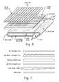
- FIG. 6depicts a display backlight.
- FIG. 7depicts a display backlight.
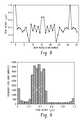
- FIGS. 8 and 10are exemplary graphical profiles of the peak heights h(j).
- FIGS. 9 and 11are a histogram of the height variation over an entire substrate with the modulation for the profiles of FIGS. 8 and 10 , respectively.
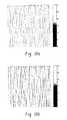
- FIGS. 12( a )- 12 ( d )illustrate exemplary modulated surface height maps from profiles taken in the w direction, wherein each profile is 1.7 mm long with a 1 micrometer sample distance.
- FIGS. 12( e )- 12 ( h )graphically illustrate exemplary autocorrelation functions for the surfaces illustrated in FIGS. 12( a )-( d ), respectively.
- FIGS. 13( a )- 13 ( d )graphically illustrate the power spectral density function of f(x) for modulated prism surfaces of FIGS. 12( a )-( d ) from profiles taken in the w direction, wherein each profile is 1.7 mm long with a 1 micrometer sample distance.
- a mere 5% (of the average pitch) lateral modulatione.g., ⁇ 2 micrometer ( ⁇ m) lateral modulation for an average 37 ⁇ m pitch
- a substantially sinusoidal height modulationwhich is periodic wherein the peak height modulation frequency is sufficient to avoid optical coupling between adjacent collimating films, wet-out can be substantially reduced or eliminated while avoiding streakiness.
- the filmcomprises a surface comprising a plurality of prism structures.
- Each prism structurecan have a lateral modulation in the w direction of less than or equal to ⁇ 20% of the average pitch of the prisms.
- the plurality of prism structurescan have a variation in prism peak height that is discrete, continuous, or a combination of both discrete and continuous.
- the prism structurescan have a height variation comprising sinusoidal function(s).
- the filmcomprises a surface comprising a plurality of prism structures.
- Each prism structurehas a lateral modulation in the w direction of ⁇ 2 ⁇ m to ⁇ 20 ⁇ m along the length of each prism in the l direction.
- the plurality of prism structureshas a sinusoidal height modulation in an h direction along the length of each prism in the l direction, with a highest prism peak height that is periodic at an interval measured in the w direction of greater than or equal to five times an average pitch.
- the average pitchis determined over a sample length in the w direction of 100 mm. Equivalently, the highest prism peak height is periodic at an interval greater than or equal to typically 2.5 meters as measured along the l direction.
- the w directionis perpendicular to the l direction.
- the modulationis less than or equal to ⁇ 10 micrometers, or less than or equal to ⁇ 5 micrometers.
- the prism structureshave a height modulation along a length l.
- the majority of prism peakscan be greater than or equal to 0.5 micrometers below the highest prism peak height for any profile taken in the w direction.
- Clusters of high peakscan contain less than or equal to 3 peaks and each cluster is separated by greater than or equal to 5 peaks, wherein a cluster is a group of adjacent peaks with a height within 0.25 micrometers of the highest prism peak height.
- the lateral modulationcan comprise a variable prism spacing.
- the height modulationcan be random or pseudo random.
- the lateral modulationcan optionally be random or pseudo random.
- the filmcan comprises a surface comprising a plurality of prism structures.
- Each prism structurehas a lateral modulation in the w direction of ⁇ 2% to ⁇ 20% of an average pitch of the prisms.
- the plurality of prism structurescan have a variation in the w direction of prism peak height that is discrete and/or continuous.
- a highest prism peak heightcan be periodic at an interval measured in the w direction of greater than or equal to five times an average pitch, wherein the average pitch is determined over a sample length in the w direction of 100 mm, wherein the interval w direction is perpendicular to the l direction.
- a majority of prism peakscan be greater than or equal to 0.5 micrometers below the highest prism peak height for any profile taken in the w direction.
- the filmcan comprise clusters of peaks, as determined in the w direction, wherein each cluster contains less than or equal to 3 peaks and each cluster is separated by greater than or equal to 5 peaks, and wherein a cluster is a group of adjacent peaks with a height within 0.25 micrometers of a highest prism peak height.
- the modulationcan be ⁇ 5% to ⁇ 10% of the average pitch.
- the prism structurescan have a height modulation in the l direction. This height modulation can random.
- the lateral modulationcan comprise a variable prism spacing. This lateral modulation can be random. The variation can be periodic and sinusoidal.
- the backlight displaycan comprise: light source(s) and film(s).
- the displaycan comprise diffuser(s), reflector(s) (e.g., pattered reflector(s)), and/or light guide(s).
- the reflector(s)can be disposed on a side of the light guide opposite the film(s).
- the diffuser(s)can be disposed on one or both sides of the film(s), wherein the films can be disposed such that the prisms structures of one film are oriented at a direction perpendicular to the prism structures of an adjacent film (e.g., as is illustrated in FIG. 6 ).
- a method for making a filmcan comprise: forming a plurality of prism structures having a lateral modulation in a w direction along a prism in the l direction on a surface of an optical substrate, wherein the lateral modulation can be ⁇ 2 ⁇ m to ⁇ 20 ⁇ m.
- the plurality of prism structurescan have a sinusoidal height profile in an h direction, wherein a highest prism peak height is periodic at an interval in the w direction of greater than or equal to five times an average pitch.
- the average pitchis determined over a sample length in the w direction of 100 mm.
- the w directionwhich is perpendicular to the l direction, is defined as illustrated in FIG. 1 .
- a method for making a filmcomprises: forming a plurality of prism structures on a surface, wherein the plurality of prism structures have a lateral modulation in the w direction of ⁇ 2% to ⁇ 20% of an average pitch of the prisms, and wherein the plurality of prism structures have a variation in the w direction of prism peak height that is discrete and/or continuous.
- One method for making an optical filmcan comprise forming a plurality of prism structures having a lateral modulation in a l direction on a surface of an optical substrate, wherein has the lateral modulation has of less than or equal to ⁇ 50% of an average pitch, or, specifically, less than or equal to ⁇ 25% of the average pitch, or, yet more specifically, ⁇ 2% to ⁇ 15% of the average pitch.
- the lateral modulationcan be less than or equal to ⁇ 20 ⁇ m
- a height modulationcan be 0.25 ⁇ m to 1.0 ⁇ m.
- the cross section a prior prism filmreveals an upper surface that is corrugated (i.e., the surface is comprised of a linear array of prism structures), each prism having straight facets, which in this illustration, are symmetrically disposed around a peak (maximum in h) for each prism in a direction w that is a lateral direction for the prism film.
- the prismsare described as a linear array since the distance between adjacent peaks has a fixed pitch in the w direction and the pitch is held constant along the length of each prism.
- the pitchis the spacing in w between adjacent peaks.
- the length dimensionis defined along a direction “l” that is normal to the page in FIG. 1 .
- the prismseach have straight sides with a peak angle 12 that is symmetric about a line 10 though the peak in the h direction.
- the peak angle 12includes the total included angle between the left and right facets ( 14 , 16 , respectively). If each facet where curved the peak angle would be the angle between the lines tangent to each facet where the facets meet at the peak.
- the peak anglecan generally be 85 to 120 degrees.
- the most popular designhas a left facet slope of +45 degrees (change in h over change in w) and a right facet slope of ⁇ 45 degrees.
- the peak anglecan be 50 to 80 degrees.
- the peakIn a front lighting film the peak can be asymmetric and the peak angle can be 0 to 30 degrees.
- the peaksare rounded or blunted (flat peaks) across a width of less than or equal to 2 micrometers ( ⁇ m), e.g., to improve abrasion resistant.
- Brightness enhancement filmstypically have a thickness (in an h direction orthogonal to w and l) of 12 micrometers to 250 micrometers. In is understood that the film can be a thicker substrate (up to several millimeters in thickness), more typically identified as a plate. In the following discussion the term film will be used throughout to identify the optical device regardless of thickness, and since brightness enhancement is not the sole application, prism film and even optical film may be used generally refer to the substrate.
- FIG. 2shows an example of a substrate (e.g., a prism film) with variable prism spacing.
- a substratee.g., a prism film
- the distance between adjacent prism peaksis not constant.
- the averagecan vary across a substrate, i.e., if, for example, ten or less adjacent peaks are used to define an average and the substrate surface comprises one hundred or more prisms (also called prism structures), the average pitch can be designed to vary. It is noted that this average is the average for the profile sample being examined, wherein the length sample in the w direction is between 0.5 mm and 100 mm.
- the peak's position for each prismcan (individually) vary in the lateral w direction along the l length direction for each prism peak as shown in FIG. 3 .
- This variationis defined as lateral modulation.
- the modulationcomprises modulating the structures (e.g., prismatic structures, and so forth) of an optical film from the nominal linear path (non varying) in a lateral direction w (direction perpendicular to the height), along the length l, by using a waveform or waveforms that are a function of l that have a nonrandom, random (or pseudo random) amplitude and/or period, wherein, here, amplitude refers to the maximum excursion perpendicular to a straight line fit to the modulated prism path.
- the amplitudecan be less than the average pitch or larger than the average pitch. As noted above, an amplitude of 4 micrometers (e.g., plus or minus 2 micrometers from center), is sufficient to eliminate streakiness.
- the modulationcan be less than or equal to ⁇ 20 micrometers, or, specifically, less than or equal to ⁇ 10 micrometers, or, more specifically, less than or equal to ⁇ 5 micrometers, or, specifically, ⁇ 2 micrometers to ⁇ 110 micrometers, e.g., for an average pitch of 37 micrometers.
- the maximum modulationcan be 2% to 100%, or, specifically, 5% to 90%, or, more specifically, 2% to 50%, or, more specifically, 10% to 25%, of the average pitch with larger modulations having the disadvantage of reduced brightness.
- the modulationis 70% to 95%, or, specifically, 75% to 90% of the average pitch.
- a filmcan have a height modulation of 0.5 micrometers ( ⁇ m) to 1 ⁇ m, and/or a lateral modulation of ⁇ 5% to ⁇ 100% of the pitch.
- Examples of lateral modulation waveformsinclude sinusoidal waveforms where the sinusoid has a random phase, frequency, or amplitude, or a combination comprising at least one of the foregoing.
- Another exampleis a waveform where the signal is produced by filtering a random noise waveform (uniform, Gaussian, or pink noise, are examples) with a band pass, low pass, or high pass filter.
- the signalcan be continuous (analog), discrete (sampled), or a combination of both.
- the lateral modulations waveform or neighboring prismscan include interactions between the prisms. For example, a two dimensional filter can be applied such that the random wave forms are filtered along the length l and also include numerical input from the noise waveforms of adjacent prisms.
- One such implementationwould be to low pass filter the noise waveforms in the l direction and high pass filter between noise waveforms in the w direction.
- the filterscan be discrete or continuous or a combination of both. In the example above the w direction filter would most likely be discrete, with the l direction filter as least approximately continuous.
- the wavelength cut offs for the various filters that can be appliedare 10 micrometers to 10 millimeters. This range can also be applied to sinusoidal components that are used for lateral modulation.
- the macroscopic blur function of a typical prism film with straight facetsresults in a double image with the image doubling effect increasing as function of the distance between the prism array surface and the object.
- Due to the various modulation paths in the randomized structure introduced herethere is an additional component to the blur function that is due to curvature of the paths.
- the effectis that of a rotation of each of the split images around an arc. This is called “bow diffusion” due to the resemblance that the blur function has to a bow tie. (See FIG. 5 )
- bow diffusiondue to the resemblance that the blur function has to a bow tie.
- increased slope in the pathresults in increased blur.
- modulation of greater than 5% or the average pitchcould be employed to address moiré effects
- lateral modulationcould be employed in combination with height modulation (modulation in peak height as a function of l or between different prisms) due to a periodic sinusoidal waveform, to reduce or eliminate periodicity induced streakiness while preventing optical coupling.
- FIGS. 6 and 7depict exemplary backlight displays.
- Light enters the display from the light sourcee.g., cold cathode fluorescent light (CCFL); one or more light emitting diodes might also be used
- the light sourcee.g., cold cathode fluorescent light (CCFL); one or more light emitting diodes might also be used
- the lightpasses through the diffuser and into the prism films where it is collimated and directed out of the display (see light out arrow).
- Light that is directed back toward the diffuseris reflected by the reflector back toward the prism film.
- the bulk statistical properties of such a filmare characterized by parameters such as optical gain and viewing angle.
- the prism films shown in the figuresmay be designed with the present disclosure, i.e. the display backlight can comprise one or more prism films.
- c f ⁇ ( x ′ )⁇ - ⁇ ⁇ ⁇ f ⁇ ( x - x ′ ) ⁇ f ⁇ ( x ) ⁇ ⁇ d x Equation ⁇ ⁇ 1
- x′is a shift in coordinate x.
- the autocorrelation function c ⁇ (x′)is symmetrical about x′ equal to zero and has a Fourier transform relationship with the power spectral density of ⁇ (x).
- the autocorrelationis used in surface metrology to categorize the different types of surfaces.
- the autocorrelation length (L c )is the distance from x′ at which c ⁇ (x′) first decreases below a threshold.
- the shorter the correlation lengththe more random the surface.
- a larger correlation lengthmeans that the surface is less random than a surface with a smaller correlation length.
- the examples in FIG. 12show autocorrelation function analysis for a 1.7 millimeter by 1.7 millimeter (mm) model of film examples with increasing random lateral modulation for each example from left to right.
- Each exampleis sampled in a 1 micrometer by 1 micrometer grid and the auto correlation function is evaluated for a 1.7 millimeter long profile taken from the w direction (height h as a function of w).
- the analysisis performed using the MATLAB analysis software standard function xcorr.m provided with MATLAB release “R12”.
- the “coeff” optionis used to provide a normalized output for zero lag (the initial value).
- the autocorrelation functionoscillates at an interval equal to the average pitch of the examples (all have 37 ⁇ m average pitch).
- the envelope of the oscillationsdrops off nearly linearly for FIG. 12( e ) ( FIG. 12( h ) with the least lateral modulation) as a function of position.
- All the other exampleshave envelopes that drop to lower values more rapidly as a function of position (increasingly so toward FIG. 13 ( h )). This drop is due to the increased randomness caused by increasing random lateral modulation.
- the value of the autocorrelation function for the three-dimensional surface of the optical substrate for a 1.7 mm sampledrops to less than or equal to 1/e ( 1/2.7183) of its initial value in a correlation length of less than or equal to 0.5 millimeter (mm). In still other embodiments, the value of the autocorrelation function drops to 1/e of its initial value in less than or equal to 0.1 mm.
- the 1.7 mm sample scanscan be taken from a lateral profile at any location on a film or other optical substrate that employs the technology.
- the correlation lengthis related to the reduction of moiré artifacts. As noted, smaller correlation length indicates a more random surface than a larger correlation length, and this smaller correlation length also relates to greater diffusion and the reduction of moiré artifacts. Because the three-dimensional surfaces of the substrates ( FIGS. 12 ( b )-( d )) are highly irregular, as indicated by the low correlation length, the substrates can be effective to reduce moiré artifacts.
- the height variation or the prism peakscan have a very long period: with a wavelength that is several times that maximum length of the prisms in the l direction of a particular substrate. This can be physically manifested as long wavelength variations in the height of a cutting tool around a drum used as a master for the films.
- the l maximum length of a substrateis equivalent to one circumferential pass around the outer diameter of a mastering drum (though this can change in other cases).
- every prismis equivalent to a ring around the drum and can be identified by drum revolution number, distance along l is equivalent to the position in rotation about the drum axis (t, with units of radians).
- the purpose of the height variationis to minimize optical coupling. This is achieved by creating height variations such that the majority of prisms do not experience optical coupling. This can be achieved by keeping the majority of prism peaks at least 0.5 micrometers below the highest prisms' peak height for any profile of a substrate as measured in the w direction (0.5 millimeters to 1.7 millimeter being a suitable measurement width a diamond stylus profilometer with a tip radius of less than 2 ⁇ m can be the instrument to verify the height variation). This distance has been found to substantially avoid contact with the lower prisms, even in the presence of a warped substrate. The net effect is that the density of contacting prisms is substantially reduced and the optical coupling effect is less prominent.
- tis related to l by a drum diameter, d, such that for each j th ring around the drum (nominally separated from each other by pitch p), l is equal to t times d. Note that since each ring corresponds to an individual prism the j th ring is equivalent to the j th prism.
- the height modulationcan be continuous along l (e.g., the height varies along the length of each prism) or discrete from ring to ring (e.g., the height does not vary along the length of each prism, but does vary between prisms), or a combination of both.
- le.g., the height varies along the length of each prism
- ringe.g., the height does not vary along the length of each prism, but does vary between prisms
- h ⁇ ( j )0.25 ⁇ ⁇ cos ⁇ ( ( ⁇ ⁇ ⁇ j period ) beta + ( 3 ⁇ ⁇ ⁇ ⁇ ⁇ j period ) beta + ( 5 ⁇ ⁇ ⁇ ⁇ ⁇ j period ) beta + ( 7 ⁇ ⁇ ⁇ ⁇ ⁇ j period ) beta )
- betais a non-linear scale factor that provides for a skewed distribution in height
- cosis the cosine function.
- a histogram of the height variation over an entire substrate with this modulationis given in FIG. 9 .
- h ( j )a 0 +a 1 cos( jw )+ b 1 sin( jw )+ a 2 cos(2 jw )+ b 2 sin(2 jw )+ a 3 cos(3 jw )+ b 3 sin(3 jw )+ a 4 cos(4 jw )+ b 4 sin(4 jw )+ a 5 cos(5 jw )+ b 5 sin(5 jw ) wherein (with the units of height being micrometers):
- this height modulationalso has the property of providing a distribution of peaks heights that keeps the majority of peak height on a level of 0.5 ⁇ m or more below the highest peaks.
- the wavesare periodic, a random waveform formed with similarly large component wavelengths (i.e., spatial frequency content) can achieve a similar effect as long as the distribution is skewed to the majority of the peaks being greater than or equal to 0.5 ⁇ m below the highest peak height (i.e., the median height is at least 0.5 ⁇ m less than the tallest peak height).
- the high peaksoccur in a cluster (adjacent peaks with a height within 0.25 micrometers of the maximum peak height) it is desirable that less than or equal to 3 peaks (or, specifically, 2 peaks) occur in each cluster and that each cluster is separated by greater than or equal to 5 lower peaks, or, specifically, greater than or equal to 8 lower peaks, (for any w direction profile).
- This separatorhelps to avoid visually objectionable large regions of wet-out.
- the occurrence of clusterdoes not have to be limited to strictly periodic but this does simplify the design of the height variation. Even when employing randomization to the height variation the long wavelengths desired tend to produce objectionable streakiness in the appearance of the films if the slight lateral modulation is not used. Note that the period of the height modulation does not need to an integer multiple of the prism pitch.
- the actual surface of the substrateswhich can have characteristic dimensions of less than or equal to 4 meters in the w and l dimensions, independently, and have good surface roughness (e.g., the facets are smooth with a an average surface roughness, R a , less than or equal to 4 nanometers (nm), desirably, less than or equal to 1 nanometer), can be generated in accordance with a number of processing techniques. These processing techniques include photolithography, gray-scale lithography, microlithography, electrical discharge machining and micromachining using hard tools to form molds or the like for the surface model described above.
- the method of making the substratescan be by mastering, electroforming, and mold forming.
- Photolithographic masteringcan be used to directly laser write to a photoresist, a gray scale mask, and/or a series of halftone masks that can be tiled.
- the photoresistcan be directly removed by the laser photons or used as a precursor to an additional process step, such as reactive ion etching (RIE).
- RIEreactive ion etching
- the geometrymight be mastered using hard tools, such as a single point diamond tool on a multi-axis mill.
- the masterwill generally be made as a negative.
- the substrate of the mastercan be glass, (fused silica for example), metal (copper or nickel for example) or plastic (polycarbonate for example).
- the mastercan be used to mold plastic parts directly or used in electroforming.
- Electroformingcan be in one multiple (e.g., two) stages, wherein the master is a positive if only one stage is used.
- the mastercan be coated with a thin metal coating (especially if the master is not inherently conductive).
- a “ father” electroformis created by electro-depositing nickel (or another material) on the master. This replica is again electroformed to create a “daughter” that is used to mold the plastic parts.
- the object that is used to mold the deviceis referred to as the mold.
- the moldcan be in the form of a belt, a drum, a plate, or a cavity.
- the moldcan be tiles from a plurality of masters or electroforms.
- the moldcan be used to form the structures on a substrate through various processing embossing (e.g., hot embossing of the substrate), calendaring (e.g., cold calendaring of the substrate) and/or through the addition of an ultraviolet curing or thermal setting material in which the structures are formed.
- the moldcan be used to form the film through various techniques such as injection molding, vacuum forming, and so forth.
- the substrate or coating materialcan be any organic, inorganic or hybrid optically transparent material and can include suspended diffusion, birefringent, and/or index of refraction, modifying particles.
- the optical substrate so formedcan be formed with an optically transparent material with an index of refraction of 1.1 to 3.0 and more particularly with an index of refraction of approximately 1.45 to 1.7.
- Ranges disclosed hereinare inclusive and combinable (e.g., ranges of “up to 25 wt %, or, more specifically, 5 wt % to 20 wt %”, is inclusive of the endpoints and all intermediate values of the ranges of “5 wt % to 25 wt %,” etc.).
- “Combination”is inclusive of blends, mixtures, alloys, reaction products, and the like.
- the terms “first,” “second,” and the like, hereindo not denote any order, quantity, or importance, but rather are used to distinguish one element from another, and the terms “a” and “an” herein do not denote a limitation of quantity, but rather denote the presence of at least one of the referenced item.
- the suffix “(s)” as used hereinis intended to include both the singular and the plural of the term that it modifies, thereby including one or more of that term (e.g., the colorant(s) includes one or more colorants).
- the notation “ ⁇ 10%”means that the indicated measurement can be from an amount that is minus 10% to an amount that is plus 10% of the stated value.
- Reference throughout the specification to “one embodiment”, “another embodiment”, “an embodiment”, and so forth,means that a particular element (e.g., feature, structure, and/or characteristic) described in connection with the embodiment is included in at least one embodiment described herein, and may or may not be present in other embodiments.
- the described elementsmay be combined in any suitable manner in the various embodiments and are not limited to the specific combination in which they are discussed.
Landscapes
- Physics & Mathematics (AREA)
- General Physics & Mathematics (AREA)
- Optics & Photonics (AREA)
- Nonlinear Science (AREA)
- Mathematical Physics (AREA)
- Chemical & Material Sciences (AREA)
- Crystallography & Structural Chemistry (AREA)
- Optical Elements Other Than Lenses (AREA)
- Planar Illumination Modules (AREA)
- Liquid Crystal (AREA)
Abstract
Description
where x′ is a shift in coordinate x. The autocorrelation function cƒ(x′) is symmetrical about x′ equal to zero and has a Fourier transform relationship with the power spectral density of ƒ(x).
Here beta is a non-linear scale factor that provides for a skewed distribution in height, cos is the cosine function. A profile of the peak heights (h(j)) is given in
h(j)=a0+a1cos(jw)+b1sin(jw)+a2cos(2jw)+b2sin(2jw)+a3cos(3jw)+b3sin(3jw)+a4cos(4jw)+b4sin(4jw)+a5cos(5jw)+b5sin(5jw)
wherein (with the units of height being micrometers):
Claims (15)
Priority Applications (5)
| Application Number | Priority Date | Filing Date | Title |
|---|---|---|---|
| US12/141,674US7859759B2 (en) | 2002-05-20 | 2008-06-18 | Film, backlight displays, and methods for making the same |
| TW098104838ATWI461750B (en) | 2008-02-26 | 2009-02-16 | Optical film, backlit display and method of manufacturing same |
| EP09715760AEP2263116A1 (en) | 2008-02-26 | 2009-02-25 | Film, backlight displays, and methods for making the same |
| PCT/US2009/035095WO2009108673A1 (en) | 2008-02-26 | 2009-02-25 | Film, backlight displays, and methods for making the same |
| CN200980114865.8ACN102016702B (en) | 2008-02-26 | 2009-02-25 | Film, backlight displays, and methods for making same |
Applications Claiming Priority (6)
| Application Number | Priority Date | Filing Date | Title |
|---|---|---|---|
| US10/150,958US6862141B2 (en) | 2002-05-20 | 2002-05-20 | Optical substrate and method of making |
| US11/019,640US7180672B2 (en) | 2002-05-20 | 2004-12-23 | Optical substrate and method of making |
| US11/460,309US7324284B2 (en) | 2002-05-20 | 2006-07-27 | Optical substrate and method of making |
| US11/979,027US7965447B2 (en) | 2002-05-20 | 2007-10-30 | Optical substrate and method of making |
| US12/037,399US20090185278A1 (en) | 2002-05-20 | 2008-02-26 | Film, backlight displays, and methods for making the same |
| US12/141,674US7859759B2 (en) | 2002-05-20 | 2008-06-18 | Film, backlight displays, and methods for making the same |
Related Parent Applications (1)
| Application Number | Title | Priority Date | Filing Date |
|---|---|---|---|
| US12/037,399Continuation-In-PartUS20090185278A1 (en) | 2002-05-20 | 2008-02-26 | Film, backlight displays, and methods for making the same |
Publications (2)
| Publication Number | Publication Date |
|---|---|
| US20090052045A1 US20090052045A1 (en) | 2009-02-26 |
| US7859759B2true US7859759B2 (en) | 2010-12-28 |
Family
ID=40467393
Family Applications (1)
| Application Number | Title | Priority Date | Filing Date |
|---|---|---|---|
| US12/141,674Expired - Fee RelatedUS7859759B2 (en) | 2002-05-20 | 2008-06-18 | Film, backlight displays, and methods for making the same |
Country Status (5)
| Country | Link |
|---|---|
| US (1) | US7859759B2 (en) |
| EP (1) | EP2263116A1 (en) |
| CN (1) | CN102016702B (en) |
| TW (1) | TWI461750B (en) |
| WO (1) | WO2009108673A1 (en) |
Cited By (6)
| Publication number | Priority date | Publication date | Assignee | Title |
|---|---|---|---|---|
| US20120099197A1 (en)* | 2006-10-30 | 2012-04-26 | Nitto Denko Corporation | Antiglare film, antiglare sheet, process for producing them, and image display apparatus using them |
| US20150338052A1 (en)* | 2014-05-22 | 2015-11-26 | Beautylight Optronics Co., Ltd | Optical film |
| US9322178B2 (en) | 2013-12-15 | 2016-04-26 | Vkr Holdings A/S | Skylight with sunlight pivot |
| USD794216S1 (en) | 2016-03-31 | 2017-08-08 | Vkr Holding A/S | Skylight cover |
| US10088621B2 (en) | 2013-12-17 | 2018-10-02 | Samsung Display Co. Ltd. | Light guide panel, backlight unit, and liquid crystal display |
| US10889990B2 (en) | 2016-03-31 | 2021-01-12 | Vkr Holding A/S | Skylight cover with advantageous topography |
Families Citing this family (6)
| Publication number | Priority date | Publication date | Assignee | Title |
|---|---|---|---|---|
| KR101747978B1 (en)* | 2009-03-31 | 2017-06-15 | 도판 인사츠 가부시키가이샤 | El panel, and illuminating device and display device using el panel |
| TWI553350B (en)* | 2009-08-11 | 2016-10-11 | 友輝光電股份有限公司 | Luminance enhancement optical substrates with anit-interference-fringe structure |
| DE102013003441A1 (en) | 2013-02-25 | 2014-09-11 | Fraunhofer-Gesellschaft zur Förderung der angewandten Forschung e.V. | Electromagnetic radiation scattering element |
| JP6050712B2 (en)* | 2013-03-27 | 2016-12-21 | 株式会社ジャパンディスプレイ | Reflective liquid crystal display device and electronic apparatus |
| TWI611218B (en)* | 2013-11-08 | 2018-01-11 | 逢甲大學 | Method for producing an optical diffuser film |
| TW201541124A (en)* | 2014-04-22 | 2015-11-01 | Beautylight Optronics Co Ltd | Optical film |
Citations (96)
| Publication number | Priority date | Publication date | Assignee | Title |
|---|---|---|---|---|
| US2403731A (en) | 1943-04-01 | 1946-07-09 | Eastman Kodak Co | Beam splitter |
| JPS5589806A (en) | 1978-12-27 | 1980-07-07 | Canon Inc | Optical making method of diffusion plate |
| JPS55120002A (en) | 1979-03-09 | 1980-09-16 | Sekisui Chem Co Ltd | Light scattering tape or sheet |
| JPS55120001A (en) | 1979-03-09 | 1980-09-16 | Sekisui Chem Co Ltd | Light scattering tape or sheet |
| US4542449A (en) | 1983-08-29 | 1985-09-17 | Canadian Patents & Development Limited | Lighting panel with opposed 45° corrugations |
| US4576850A (en) | 1978-07-20 | 1986-03-18 | Minnesota Mining And Manufacturing Company | Shaped plastic articles having replicated microstructure surfaces |
| US4906070A (en) | 1985-11-21 | 1990-03-06 | Minnesota Mining And Manufacturing Company | Totally internally reflecting thin, flexible film |
| JPH0272388A (en) | 1988-09-07 | 1990-03-12 | Hitachi Ltd | Lighting device |
| JPH02221926A (en) | 1989-02-23 | 1990-09-04 | Asahi Chem Ind Co Ltd | Diffusion plate made of methacrylic resin and its production |
| US4984144A (en) | 1987-05-08 | 1991-01-08 | Minnesota Mining And Manufacturing Company | High aspect ratio light fixture and film for use therein |
| US5005108A (en) | 1989-02-10 | 1991-04-02 | Lumitex, Inc. | Thin panel illuminator |
| US5056892A (en) | 1985-11-21 | 1991-10-15 | Minnesota Mining And Manufacturing Company | Totally internally reflecting thin, flexible film |
| JPH04303802A (en) | 1991-03-30 | 1992-10-27 | Sekisui Chem Co Ltd | Light diffusion sheet |
| JPH0560908A (en) | 1990-12-17 | 1993-03-12 | Mitsubishi Rayon Co Ltd | Surface light source device and production therefor and dry film resist used therefor |
| JPH05142422A (en) | 1991-11-20 | 1993-06-11 | Nec Kansai Ltd | Plane light emitting unit and production thereof |
| JPH05173134A (en) | 1991-12-26 | 1993-07-13 | Sekisui Chem Co Ltd | Dimming sheet |
| JPH05313004A (en) | 1992-05-07 | 1993-11-26 | Sekisui Chem Co Ltd | Light adjusting sheet and liquid crystal display device provided with the sheet |
| JPH0618707A (en) | 1992-06-30 | 1994-01-28 | Dainippon Printing Co Ltd | Lenticular lens, surface light source and liquid crystal display device |
| JPH0627325A (en) | 1992-07-07 | 1994-02-04 | Sekisui Chem Co Ltd | Surface light source device |
| JPH0643310A (en) | 1992-07-27 | 1994-02-18 | Sekisui Chem Co Ltd | Film or sheet for surface light source device |
| JPH0682634A (en) | 1992-07-07 | 1994-03-25 | Sekisui Chem Co Ltd | Surface light source device |
| US5303322A (en) | 1992-03-23 | 1994-04-12 | Nioptics Corporation | Tapered multilayer luminaire devices |
| JPH06138308A (en) | 1992-10-28 | 1994-05-20 | Taiho Ind Co Ltd | Light diffusing plate |
| JPH06148408A (en) | 1992-11-11 | 1994-05-27 | Sekisui Chem Co Ltd | Optical control sheet |
| JPH06186562A (en) | 1992-10-23 | 1994-07-08 | Sawaki:Kk | Light transmission plate for surface light source |
| US5390276A (en) | 1992-10-08 | 1995-02-14 | Briteview Technologies | Backlighting assembly utilizing microprisms and especially suitable for use with a liquid crystal display |
| JPH07104109A (en) | 1993-10-04 | 1995-04-21 | Sekisui Chem Co Ltd | Production of light diffusion film or sheet |
| US5439621A (en) | 1993-04-12 | 1995-08-08 | Minnesota Mining And Manufacturing Company | Method of making an array of variable focal length microlenses |
| JPH07230001A (en) | 1993-05-17 | 1995-08-29 | Sekisui Chem Co Ltd | Optical control sheet and its manufacture |
| JPH08146418A (en) | 1994-11-24 | 1996-06-07 | Sekisui Chem Co Ltd | Film for improvement in image quality for liquid crystal display device |
| JPH08160203A (en) | 1994-12-07 | 1996-06-21 | Sekisui Chem Co Ltd | Picture quality improving film for liquid crystal display |
| JPH08220344A (en) | 1995-02-15 | 1996-08-30 | Fujitsu Ltd | Flat light source and non-emissive display device |
| US5552907A (en) | 1992-01-27 | 1996-09-03 | Sekisui Chemical Co., Ltd. | Light adjusting sheet having a sinusoidal surface and a non-optically flat surface and useable with an LCD |
| US5557836A (en) | 1993-10-20 | 1996-09-24 | Minnesota Mining And Manufacturing Company | Method of manufacturing a cube corner article |
| US5564870A (en) | 1993-10-20 | 1996-10-15 | Minnesota Mining And Manufacturing Company | Method of manufacturing an asymmetric cube corner article |
| JPH08286629A (en) | 1995-04-17 | 1996-11-01 | Sekisui Chem Co Ltd | Light-collecting sheet |
| JPH08313710A (en) | 1995-05-12 | 1996-11-29 | Mitsubishi Rayon Co Ltd | Prism sheet and backlight |
| JPH09145932A (en) | 1995-11-24 | 1997-06-06 | Konica Corp | Back light and optical sheet |
| JPH09304607A (en) | 1996-05-16 | 1997-11-28 | Nitto Denko Corp | Light diffusion film |
| US5764315A (en) | 1992-01-27 | 1998-06-09 | Sekisui Chemical Co., Ltd. | Light adjusting sheet for a planar lighting device and a planar lighting device and a liquid crystal display using the sheet |
| US5771328A (en) | 1995-03-03 | 1998-06-23 | Minnesota Mining And Manufacturing Company | Light directing film having variable height structured surface and light directing article constructed therefrom |
| US5769522A (en) | 1991-09-09 | 1998-06-23 | Enplas Corporation | Surface light source device |
| WO1998033006A2 (en) | 1997-01-13 | 1998-07-30 | Minnesota Mining And Manufacturing Company | Luminaire device |
| US5808784A (en) | 1994-09-06 | 1998-09-15 | Dai Nippon Printing Co., Ltd. | Lens array sheet surface light source, and transmission type display device |
| US5851062A (en) | 1995-08-11 | 1998-12-22 | Omron Corporation | Prism sheet for surface light source |
| US5861990A (en) | 1996-03-08 | 1999-01-19 | Kaiser Optical Systems | Combined optical diffuser and light concentrator |
| US5876107A (en) | 1995-06-27 | 1999-03-02 | Lumitex, Inc. | Light emitting panel assemblies |
| US5887964A (en) | 1995-08-01 | 1999-03-30 | Nitto Jushi Kogyo Kabushiki Kaisha | Surface light source device and liquid crystal display |
| US5917664A (en) | 1996-02-05 | 1999-06-29 | 3M Innovative Properties Company | Brightness enhancement film with soft cutoff |
| US5919551A (en) | 1996-04-12 | 1999-07-06 | 3M Innovative Properties Company | Variable pitch structured optical film |
| US5944405A (en) | 1994-08-12 | 1999-08-31 | Dai Nippon Printing Co., Ltd. | Flat light source using light-diffusing sheet with projections thereon |
| US5982540A (en) | 1994-03-16 | 1999-11-09 | Enplas Corporation | Surface light source device with polarization function |
| WO1999063394A1 (en) | 1998-06-02 | 1999-12-09 | Nissha Printing Co., Ltd. | Touch screen with front lighting |
| US6002829A (en) | 1992-03-23 | 1999-12-14 | Minnesota Mining And Manufacturing Company | Luminaire device |
| US6052164A (en) | 1993-03-01 | 2000-04-18 | 3M Innovative Properties Company | Electroluminescent display with brightness enhancement |
| US6091547A (en) | 1994-09-27 | 2000-07-18 | 3M Innovative Properties Company | Luminance control film |
| US6108131A (en) | 1998-05-14 | 2000-08-22 | Moxtek | Polarizer apparatus for producing a generally polarized beam of light |
| US6208463B1 (en) | 1998-05-14 | 2001-03-27 | Moxtek | Polarizer apparatus for producing a generally polarized beam of light |
| US6213606B1 (en) | 1996-09-30 | 2001-04-10 | Digital Optics International | Image projection system |
| US6243068B1 (en) | 1998-05-29 | 2001-06-05 | Silicon Graphics, Inc. | Liquid crystal flat panel display with enhanced backlight brightness and specially selected light sources |
| JP2001166113A (en) | 1999-12-08 | 2001-06-22 | Dainippon Printing Co Ltd | Condensing film, surface light source device and liquid crystal display device |
| JP2001183642A (en) | 1999-12-24 | 2001-07-06 | Toppan Printing Co Ltd | Multi-prism sheet and liquid crystal display device using the same |
| US6275310B1 (en) | 2000-05-22 | 2001-08-14 | The United States Of America As Represented By The Secretary Of The Air Force | Modified minimum distance criterion for blended random and nonrandom encoding |
| US6277471B1 (en) | 1999-06-18 | 2001-08-21 | Shih Chieh Tang | Brightness enhancement film |
| US6280063B1 (en) | 1997-05-09 | 2001-08-28 | 3M Innovative Properties Company | Brightness enhancement article |
| US6290364B1 (en) | 1993-04-05 | 2001-09-18 | Enplas Corporation | Surface light source device |
| US6322236B1 (en) | 1999-02-09 | 2001-11-27 | 3M Innovative Properties Company | Optical film with defect-reducing surface and method for making same |
| US20010051264A1 (en) | 1993-10-29 | 2001-12-13 | Mieczyslaw H. Mazurek | Pressure-sensitive adhesives having microstructured surfaces |
| US6356391B1 (en) | 1999-10-08 | 2002-03-12 | 3M Innovative Properties Company | Optical film with variable angle prisms |
| US6354709B1 (en) | 1998-02-18 | 2002-03-12 | 3M Innovative Properties Company | Optical film |
| US20020080598A1 (en) | 1999-02-23 | 2002-06-27 | Parker Jeffery R. | Transreflectors, transreflector systems and displays and methods of making transreflectors |
| US20020097496A1 (en) | 2000-12-15 | 2002-07-25 | Reflexite Corporation | Light redirecting film |
| US6456437B1 (en) | 1999-01-14 | 2002-09-24 | 3M Innovative Properties Company | Optical sheets suitable for spreading light |
| US20030035231A1 (en) | 2001-08-03 | 2003-02-20 | Epstein Kenneth A. | Optical film having microreplicated structures; and methods |
| US6535788B1 (en) | 1998-09-14 | 2003-03-18 | Makino Milling Machine Co., Ldt | Machining apparatus |
| US6576887B2 (en) | 2001-08-15 | 2003-06-10 | 3M Innovative Properties Company | Light guide for use with backlit display |
| US6701211B2 (en) | 2001-09-10 | 2004-03-02 | Siemens Aktiengesellschaft | Computer-aided control method for a machine tool |
| US20040051987A1 (en) | 2000-09-29 | 2004-03-18 | Stefan Bauer | Optical substrate and method and apparatus for producing optical substrates |
| US6759113B1 (en) | 2003-03-24 | 2004-07-06 | Shih-Chieh Tang | Uniform curved surface structure of a brightness unit for a brightness enhancement film |
| US6811274B2 (en) | 2002-12-04 | 2004-11-02 | General Electric Company | Polarization sensitive optical substrate |
| US6846098B2 (en) | 2002-05-16 | 2005-01-25 | Eastman Kodak Company | Light diffuser with variable diffusion |
| US6862141B2 (en) | 2002-05-20 | 2005-03-01 | General Electric Company | Optical substrate and method of making |
| US6900941B2 (en) | 2002-05-16 | 2005-05-31 | Eastman Kodak Company | Light diffuser with colored variable diffusion |
| US6952627B2 (en) | 2002-12-18 | 2005-10-04 | General Electric Company | Method and apparatus for fabricating light management substrates |
| US6975455B1 (en) | 2000-04-18 | 2005-12-13 | 3M Innovative Properties Company | Transflective layer for displays |
| US20060056031A1 (en) | 2004-09-10 | 2006-03-16 | Capaldo Kevin P | Brightness enhancement film, and methods of making and using the same |
| JP2006082645A (en) | 2004-09-15 | 2006-03-30 | Kubota Corp | Constant mesh transmission switching device |
| US20060226583A1 (en) | 2005-04-04 | 2006-10-12 | Marushin Patrick H | Light directing film |
| US7125131B2 (en) | 2002-12-06 | 2006-10-24 | General Electric Company | Brightness enhancement film with improved view angle |
| US7142767B2 (en) | 2003-12-31 | 2006-11-28 | 3M Innovative Properties Company | Scratch-resistant light directing films |
| US20070031140A1 (en) | 2005-08-04 | 2007-02-08 | Biernath Rolf W | Article having a birefringent surface and microstructured features having a variable pitch or angles for use as a blur filter |
| US7180672B2 (en) | 2002-05-20 | 2007-02-20 | General Electric Company | Optical substrate and method of making |
| US7179513B2 (en) | 2003-09-12 | 2007-02-20 | 3M Innovative Properties Company | Durable optical element |
| US7221847B2 (en) | 1999-10-08 | 2007-05-22 | 3M Innovative Properties Company | Optical elements having programmed optical structures |
| US7384173B2 (en) | 2004-12-30 | 2008-06-10 | 3M Innovative Properties Company | Brightness enhancement article |
| WO2008126975A1 (en) | 2007-04-13 | 2008-10-23 | Lg Electronics Inc. | Optical film and backlight unit having the same |
Family Cites Families (2)
| Publication number | Priority date | Publication date | Assignee | Title |
|---|---|---|---|---|
| US6423068B1 (en)* | 2000-10-18 | 2002-07-23 | Erhard Reisberg | Method and apparatus for mandibular osteosynthesis |
| CN1932610A (en)* | 2005-09-16 | 2007-03-21 | 财团法人工业技术研究院 | Brightness enhancement module and light source device |
- 2008
- 2008-06-18USUS12/141,674patent/US7859759B2/ennot_activeExpired - Fee Related
- 2009
- 2009-02-16TWTW098104838Apatent/TWI461750B/ennot_activeIP Right Cessation
- 2009-02-25EPEP09715760Apatent/EP2263116A1/ennot_activeWithdrawn
- 2009-02-25CNCN200980114865.8Apatent/CN102016702B/enactiveActive
- 2009-02-25WOPCT/US2009/035095patent/WO2009108673A1/enactiveApplication Filing
Patent Citations (102)
| Publication number | Priority date | Publication date | Assignee | Title |
|---|---|---|---|---|
| US2403731A (en) | 1943-04-01 | 1946-07-09 | Eastman Kodak Co | Beam splitter |
| US4576850A (en) | 1978-07-20 | 1986-03-18 | Minnesota Mining And Manufacturing Company | Shaped plastic articles having replicated microstructure surfaces |
| JPS5589806A (en) | 1978-12-27 | 1980-07-07 | Canon Inc | Optical making method of diffusion plate |
| JPS55120002A (en) | 1979-03-09 | 1980-09-16 | Sekisui Chem Co Ltd | Light scattering tape or sheet |
| JPS55120001A (en) | 1979-03-09 | 1980-09-16 | Sekisui Chem Co Ltd | Light scattering tape or sheet |
| US4542449A (en) | 1983-08-29 | 1985-09-17 | Canadian Patents & Development Limited | Lighting panel with opposed 45° corrugations |
| US5056892A (en) | 1985-11-21 | 1991-10-15 | Minnesota Mining And Manufacturing Company | Totally internally reflecting thin, flexible film |
| US4906070A (en) | 1985-11-21 | 1990-03-06 | Minnesota Mining And Manufacturing Company | Totally internally reflecting thin, flexible film |
| US4984144A (en) | 1987-05-08 | 1991-01-08 | Minnesota Mining And Manufacturing Company | High aspect ratio light fixture and film for use therein |
| JPH0272388A (en) | 1988-09-07 | 1990-03-12 | Hitachi Ltd | Lighting device |
| US5005108A (en) | 1989-02-10 | 1991-04-02 | Lumitex, Inc. | Thin panel illuminator |
| JPH02221926A (en) | 1989-02-23 | 1990-09-04 | Asahi Chem Ind Co Ltd | Diffusion plate made of methacrylic resin and its production |
| JPH0560908A (en) | 1990-12-17 | 1993-03-12 | Mitsubishi Rayon Co Ltd | Surface light source device and production therefor and dry film resist used therefor |
| JPH04303802A (en) | 1991-03-30 | 1992-10-27 | Sekisui Chem Co Ltd | Light diffusion sheet |
| US5769522A (en) | 1991-09-09 | 1998-06-23 | Enplas Corporation | Surface light source device |
| JPH05142422A (en) | 1991-11-20 | 1993-06-11 | Nec Kansai Ltd | Plane light emitting unit and production thereof |
| JPH05173134A (en) | 1991-12-26 | 1993-07-13 | Sekisui Chem Co Ltd | Dimming sheet |
| US5764315A (en) | 1992-01-27 | 1998-06-09 | Sekisui Chemical Co., Ltd. | Light adjusting sheet for a planar lighting device and a planar lighting device and a liquid crystal display using the sheet |
| US5552907A (en) | 1992-01-27 | 1996-09-03 | Sekisui Chemical Co., Ltd. | Light adjusting sheet having a sinusoidal surface and a non-optically flat surface and useable with an LCD |
| US6335999B1 (en) | 1992-03-23 | 2002-01-01 | Minnesota Mining & Mfg. Co. | Multilayer luminaire device |
| US20020061178A1 (en) | 1992-03-23 | 2002-05-23 | Roland Winston | Luminaire device |
| US5303322A (en) | 1992-03-23 | 1994-04-12 | Nioptics Corporation | Tapered multilayer luminaire devices |
| US6002829A (en) | 1992-03-23 | 1999-12-14 | Minnesota Mining And Manufacturing Company | Luminaire device |
| JPH05313004A (en) | 1992-05-07 | 1993-11-26 | Sekisui Chem Co Ltd | Light adjusting sheet and liquid crystal display device provided with the sheet |
| JPH0618707A (en) | 1992-06-30 | 1994-01-28 | Dainippon Printing Co Ltd | Lenticular lens, surface light source and liquid crystal display device |
| JPH0682634A (en) | 1992-07-07 | 1994-03-25 | Sekisui Chem Co Ltd | Surface light source device |
| JPH0627325A (en) | 1992-07-07 | 1994-02-04 | Sekisui Chem Co Ltd | Surface light source device |
| JPH0643310A (en) | 1992-07-27 | 1994-02-18 | Sekisui Chem Co Ltd | Film or sheet for surface light source device |
| US5390276A (en) | 1992-10-08 | 1995-02-14 | Briteview Technologies | Backlighting assembly utilizing microprisms and especially suitable for use with a liquid crystal display |
| JPH06186562A (en) | 1992-10-23 | 1994-07-08 | Sawaki:Kk | Light transmission plate for surface light source |
| JPH06138308A (en) | 1992-10-28 | 1994-05-20 | Taiho Ind Co Ltd | Light diffusing plate |
| JPH06148408A (en) | 1992-11-11 | 1994-05-27 | Sekisui Chem Co Ltd | Optical control sheet |
| US6052164A (en) | 1993-03-01 | 2000-04-18 | 3M Innovative Properties Company | Electroluminescent display with brightness enhancement |
| US6290364B1 (en) | 1993-04-05 | 2001-09-18 | Enplas Corporation | Surface light source device |
| US5439621A (en) | 1993-04-12 | 1995-08-08 | Minnesota Mining And Manufacturing Company | Method of making an array of variable focal length microlenses |
| JPH07230001A (en) | 1993-05-17 | 1995-08-29 | Sekisui Chem Co Ltd | Optical control sheet and its manufacture |
| JPH07104109A (en) | 1993-10-04 | 1995-04-21 | Sekisui Chem Co Ltd | Production of light diffusion film or sheet |
| US5557836A (en) | 1993-10-20 | 1996-09-24 | Minnesota Mining And Manufacturing Company | Method of manufacturing a cube corner article |
| US5564870A (en) | 1993-10-20 | 1996-10-15 | Minnesota Mining And Manufacturing Company | Method of manufacturing an asymmetric cube corner article |
| US20010051264A1 (en) | 1993-10-29 | 2001-12-13 | Mieczyslaw H. Mazurek | Pressure-sensitive adhesives having microstructured surfaces |
| US5982540A (en) | 1994-03-16 | 1999-11-09 | Enplas Corporation | Surface light source device with polarization function |
| US5944405A (en) | 1994-08-12 | 1999-08-31 | Dai Nippon Printing Co., Ltd. | Flat light source using light-diffusing sheet with projections thereon |
| US5808784A (en) | 1994-09-06 | 1998-09-15 | Dai Nippon Printing Co., Ltd. | Lens array sheet surface light source, and transmission type display device |
| US6091547A (en) | 1994-09-27 | 2000-07-18 | 3M Innovative Properties Company | Luminance control film |
| JPH08146418A (en) | 1994-11-24 | 1996-06-07 | Sekisui Chem Co Ltd | Film for improvement in image quality for liquid crystal display device |
| JPH08160203A (en) | 1994-12-07 | 1996-06-21 | Sekisui Chem Co Ltd | Picture quality improving film for liquid crystal display |
| JPH08220344A (en) | 1995-02-15 | 1996-08-30 | Fujitsu Ltd | Flat light source and non-emissive display device |
| US5771328A (en) | 1995-03-03 | 1998-06-23 | Minnesota Mining And Manufacturing Company | Light directing film having variable height structured surface and light directing article constructed therefrom |
| JPH08286629A (en) | 1995-04-17 | 1996-11-01 | Sekisui Chem Co Ltd | Light-collecting sheet |
| JPH08313710A (en) | 1995-05-12 | 1996-11-29 | Mitsubishi Rayon Co Ltd | Prism sheet and backlight |
| US5876107A (en) | 1995-06-27 | 1999-03-02 | Lumitex, Inc. | Light emitting panel assemblies |
| US5887964A (en) | 1995-08-01 | 1999-03-30 | Nitto Jushi Kogyo Kabushiki Kaisha | Surface light source device and liquid crystal display |
| US5851062A (en) | 1995-08-11 | 1998-12-22 | Omron Corporation | Prism sheet for surface light source |
| JPH09145932A (en) | 1995-11-24 | 1997-06-06 | Konica Corp | Back light and optical sheet |
| US5917664A (en) | 1996-02-05 | 1999-06-29 | 3M Innovative Properties Company | Brightness enhancement film with soft cutoff |
| US5861990A (en) | 1996-03-08 | 1999-01-19 | Kaiser Optical Systems | Combined optical diffuser and light concentrator |
| US5919551A (en) | 1996-04-12 | 1999-07-06 | 3M Innovative Properties Company | Variable pitch structured optical film |
| JPH09304607A (en) | 1996-05-16 | 1997-11-28 | Nitto Denko Corp | Light diffusion film |
| US6213606B1 (en) | 1996-09-30 | 2001-04-10 | Digital Optics International | Image projection system |
| WO1998033006A2 (en) | 1997-01-13 | 1998-07-30 | Minnesota Mining And Manufacturing Company | Luminaire device |
| US6280063B1 (en) | 1997-05-09 | 2001-08-28 | 3M Innovative Properties Company | Brightness enhancement article |
| US6354709B1 (en) | 1998-02-18 | 2002-03-12 | 3M Innovative Properties Company | Optical film |
| US20020101659A1 (en) | 1998-05-14 | 2002-08-01 | Hansen Douglas P. | Polarizer apparatus for producing a generally polarized beam of light |
| US6208463B1 (en) | 1998-05-14 | 2001-03-27 | Moxtek | Polarizer apparatus for producing a generally polarized beam of light |
| US6108131A (en) | 1998-05-14 | 2000-08-22 | Moxtek | Polarizer apparatus for producing a generally polarized beam of light |
| US6243068B1 (en) | 1998-05-29 | 2001-06-05 | Silicon Graphics, Inc. | Liquid crystal flat panel display with enhanced backlight brightness and specially selected light sources |
| WO1999063394A1 (en) | 1998-06-02 | 1999-12-09 | Nissha Printing Co., Ltd. | Touch screen with front lighting |
| US6535788B1 (en) | 1998-09-14 | 2003-03-18 | Makino Milling Machine Co., Ldt | Machining apparatus |
| US6456437B1 (en) | 1999-01-14 | 2002-09-24 | 3M Innovative Properties Company | Optical sheets suitable for spreading light |
| US6322236B1 (en) | 1999-02-09 | 2001-11-27 | 3M Innovative Properties Company | Optical film with defect-reducing surface and method for making same |
| US20020080598A1 (en) | 1999-02-23 | 2002-06-27 | Parker Jeffery R. | Transreflectors, transreflector systems and displays and methods of making transreflectors |
| US6277471B1 (en) | 1999-06-18 | 2001-08-21 | Shih Chieh Tang | Brightness enhancement film |
| US6707611B2 (en) | 1999-10-08 | 2004-03-16 | 3M Innovative Properties Company | Optical film with variable angle prisms |
| US6356391B1 (en) | 1999-10-08 | 2002-03-12 | 3M Innovative Properties Company | Optical film with variable angle prisms |
| US7221847B2 (en) | 1999-10-08 | 2007-05-22 | 3M Innovative Properties Company | Optical elements having programmed optical structures |
| JP2001166113A (en) | 1999-12-08 | 2001-06-22 | Dainippon Printing Co Ltd | Condensing film, surface light source device and liquid crystal display device |
| JP2001183642A (en) | 1999-12-24 | 2001-07-06 | Toppan Printing Co Ltd | Multi-prism sheet and liquid crystal display device using the same |
| US6975455B1 (en) | 2000-04-18 | 2005-12-13 | 3M Innovative Properties Company | Transflective layer for displays |
| US6275310B1 (en) | 2000-05-22 | 2001-08-14 | The United States Of America As Represented By The Secretary Of The Air Force | Modified minimum distance criterion for blended random and nonrandom encoding |
| US20040051987A1 (en) | 2000-09-29 | 2004-03-18 | Stefan Bauer | Optical substrate and method and apparatus for producing optical substrates |
| US20020097496A1 (en) | 2000-12-15 | 2002-07-25 | Reflexite Corporation | Light redirecting film |
| US20030035231A1 (en) | 2001-08-03 | 2003-02-20 | Epstein Kenneth A. | Optical film having microreplicated structures; and methods |
| US6576887B2 (en) | 2001-08-15 | 2003-06-10 | 3M Innovative Properties Company | Light guide for use with backlit display |
| US6701211B2 (en) | 2001-09-10 | 2004-03-02 | Siemens Aktiengesellschaft | Computer-aided control method for a machine tool |
| US6900941B2 (en) | 2002-05-16 | 2005-05-31 | Eastman Kodak Company | Light diffuser with colored variable diffusion |
| US6846098B2 (en) | 2002-05-16 | 2005-01-25 | Eastman Kodak Company | Light diffuser with variable diffusion |
| US6862141B2 (en) | 2002-05-20 | 2005-03-01 | General Electric Company | Optical substrate and method of making |
| US7180672B2 (en) | 2002-05-20 | 2007-02-20 | General Electric Company | Optical substrate and method of making |
| US20080106793A1 (en) | 2002-05-20 | 2008-05-08 | Sabic Innovative Plastics Ip Bv | Optical substrate and method of making |
| US6811274B2 (en) | 2002-12-04 | 2004-11-02 | General Electric Company | Polarization sensitive optical substrate |
| US7125131B2 (en) | 2002-12-06 | 2006-10-24 | General Electric Company | Brightness enhancement film with improved view angle |
| US6952627B2 (en) | 2002-12-18 | 2005-10-04 | General Electric Company | Method and apparatus for fabricating light management substrates |
| US7251079B2 (en) | 2003-02-28 | 2007-07-31 | General Electric Company | Brightness enhancement film, and methods of making and using the same |
| US6759113B1 (en) | 2003-03-24 | 2004-07-06 | Shih-Chieh Tang | Uniform curved surface structure of a brightness unit for a brightness enhancement film |
| US7179513B2 (en) | 2003-09-12 | 2007-02-20 | 3M Innovative Properties Company | Durable optical element |
| US7142767B2 (en) | 2003-12-31 | 2006-11-28 | 3M Innovative Properties Company | Scratch-resistant light directing films |
| US20060056031A1 (en) | 2004-09-10 | 2006-03-16 | Capaldo Kevin P | Brightness enhancement film, and methods of making and using the same |
| JP2006082645A (en) | 2004-09-15 | 2006-03-30 | Kubota Corp | Constant mesh transmission switching device |
| US7384173B2 (en) | 2004-12-30 | 2008-06-10 | 3M Innovative Properties Company | Brightness enhancement article |
| US20060226583A1 (en) | 2005-04-04 | 2006-10-12 | Marushin Patrick H | Light directing film |
| US20070031140A1 (en) | 2005-08-04 | 2007-02-08 | Biernath Rolf W | Article having a birefringent surface and microstructured features having a variable pitch or angles for use as a blur filter |
| WO2008126975A1 (en) | 2007-04-13 | 2008-10-23 | Lg Electronics Inc. | Optical film and backlight unit having the same |
Non-Patent Citations (41)
| Title |
|---|
| 3M Innovation; 3M Brightness Enhancement Film (III) Advertisement; 1998; 6 pages. |
| A. Tagaya, Y. Koike; "Highly Scattering Optical Transmission Polymers for Bright Display"; Macromol. Symp., vol. 154; Published: 2000; pp. 73-82. |
| Backlight Optics; Accessed: Feb. 14, 2003; pp. F-2/37-F-2/44. |
| Chinese Application No. 2003801063633; Text of the First Office Action; Received: Jun. 12, 2007; 3 Pages. |
| David J. Whitehouse; Handbook of Surface Metrology; IOP Publishing Ltd.: 1994; pp. 49-58. |
| International Search Report; International Application No. PCT/US03/39178; International Filing Date: Dec. 9, 2003; Date of Mailing: May 26, 2004; 9 Pages. |
| International Search Report; International Application No. PCT/US2009/035095; International Filing Date: Feb. 25, 2009, Date of Mailing: Apr. 29, 2009, 7 Pages. |
| Japanese Patent No. 2001166113 (A); Publication Date: Jun. 22, 2001; Abstract Only; 1 Page. |
| Japanese Patent No. 2001183642 (A); Publication Date: Jul. 6, 2001; Abstract Only; 1 Page. |
| Japanese Patent No. 2006082645 (A); Publication Date: Mar. 30, 2006; Abstract Only; 1 Page. |
| Japanese Patent No. 2072388 (A); Publication Date: Mar. 12, 1990; Abstract Only; 1 Page. |
| Japanese Patent No. 2221926 (A); Publication Date: Sep. 4, 1990; Abstract Only; 1 Page. |
| Japanese Patent No. 2277002 (A); Publication Date: Nov. 13, 1990; Abstract Only; 1 Page. |
| Japanese Patent No. 4303802 (A); Publication Date: Oct. 27, 1992; Abstract Only; 1 Page. |
| Japanese Patent No. 5060908 (A); Publication Date: Mar. 12, 1993; Abstract Only; 1 Page. |
| Japanese Patent No. 5142422 (A); Publication Date: Jun. 11, 1993; Abstract Only; 1 Page. |
| Japanese Patent No. 5173134 (A); Publication Date: Jul. 13, 1993; Abstract Only; 1 Page. |
| Japanese Patent No. 5313004 (A); Publication Date: Nov. 26, 1993; Abstract Only; 1 Page. |
| Japanese Patent No. 55089806 (A); Publication Date: Jul. 7, 1980; Abstract Only; 1 Page. |
| Japanese Patent No. 55120001 (A); Publication Date: Sep. 16, 1980; Abstract Only; 1 Page. |
| Japanese Patent No. 55120002 (A); Publication Date: Sep. 16, 1980; Abstract Only; 1 Page. |
| Japanese Patent No. 6018707 (A); Publication Date: Jan. 28, 1994; Abstract Only; 1 Page. |
| Japanese Patent No. 6027325 (A); Publication Date: Feb. 4, 1994; Abstract Only; 1 Page. |
| Japanese Patent No. 6043310 (A); Publication Date: Feb. 18, 1994; Abstract Only; 1 Page. |
| Japanese Patent No. 6082634 (A); Publication Date: Mar. 25, 1994; Abstract Only; 1 Page. |
| Japanese Patent No. 6138308 (A); Publication Date: May 20, 1994; Abstract Only; 1 Page. |
| Japanese Patent No. 6148408 (A); Publication Date: May 27, 1994; Abstract Only; 1 Page. |
| Japanese Patent No. 6186562 (A); Publication Date: Jul. 8, 1994; Abstract Only; 1 Page. |
| Japanese Patent No. 7104109 (A); Publication Date: Apr. 21, 1995; Abstract Only; 1 Page. |
| Japanese Patent No. 7230001 (A); Publication Date: Aug. 29, 1995; Abstract Only; 1 Page. |
| Japanese Patent No. 8146418 (A); Publication Date: Jun. 7, 1996; Abstract Only; 1 Page. |
| Japanese Patent No. 8160203 (A); Publication Date: Jun. 21, 1996; Abstract Only; 1 Page. |
| Japanese Patent No. 8220344 (A); Publication Date: Aug. 30, 1996; Abstract Only; 1 Page. |
| Japanese Patent No. 8286629 (A); Publication Date: Nov. 1, 1996; Abstract Only; 1 Page. |
| Japanese Patent No. 8313710 (A); Publication Date: Nov. 29, 1996; Abstract Only; 1 Page. |
| Japanese Patent No. 9145932 (A); Publication Date: Jun. 6, 1997; Abstract Only; 1 Page. |
| Japanese Patent No. 9304607 (A); Publication Date: Nov. 28, 1997; Abstract Only; 1 Page. |
| Machine Design; "Plastic Film Reflects Around the Corner"; Aug. 1997; p. 52. |
| Max Levy Autograph, Inc. MLA 4000 Series Ultra Precision Micro Machining/Contouring System; Bulletin 2050; Advertisement; 1998; 6 pages. |
| S.G. Saxe; Solar Energy Materials; Prismatic Film Light Guides: Performance and Recent Developments; vol. 10, No. 95-109; Published: 1989; North-Holland, Amsterdam; pp. 95-109. |
| Written Opinion of the International Searching Authority; International Application No. PCT/US2009/035095; International Filing Date: Feb. 25, 2009; Date of Mailing: Apr. 29, 2009, 8 Pages. |
Cited By (9)
| Publication number | Priority date | Publication date | Assignee | Title |
|---|---|---|---|---|
| US20120099197A1 (en)* | 2006-10-30 | 2012-04-26 | Nitto Denko Corporation | Antiglare film, antiglare sheet, process for producing them, and image display apparatus using them |
| US8537467B2 (en)* | 2006-10-30 | 2013-09-17 | Nitto Denko Corporation | Antiglare film, antiglare sheet, process for producing them, and image display apparatus using them |
| US9322178B2 (en) | 2013-12-15 | 2016-04-26 | Vkr Holdings A/S | Skylight with sunlight pivot |
| US10088621B2 (en) | 2013-12-17 | 2018-10-02 | Samsung Display Co. Ltd. | Light guide panel, backlight unit, and liquid crystal display |
| US10330846B2 (en) | 2013-12-17 | 2019-06-25 | Samsung Display Co. Ltd. | Light guide panel, backlight unit, and liquid crystal display |
| US20150338052A1 (en)* | 2014-05-22 | 2015-11-26 | Beautylight Optronics Co., Ltd | Optical film |
| US9347641B2 (en)* | 2014-05-22 | 2016-05-24 | Beautylight Optronics Co., Ltd | Optical film |
| USD794216S1 (en) | 2016-03-31 | 2017-08-08 | Vkr Holding A/S | Skylight cover |
| US10889990B2 (en) | 2016-03-31 | 2021-01-12 | Vkr Holding A/S | Skylight cover with advantageous topography |
Also Published As
| Publication number | Publication date |
|---|---|
| TW200951507A (en) | 2009-12-16 |
| US20090052045A1 (en) | 2009-02-26 |
| WO2009108673A1 (en) | 2009-09-03 |
| CN102016702B (en) | 2014-03-12 |
| EP2263116A1 (en) | 2010-12-22 |
| TWI461750B (en) | 2014-11-21 |
| CN102016702A (en) | 2011-04-13 |
Similar Documents
| Publication | Publication Date | Title |
|---|---|---|
| US7859759B2 (en) | Film, backlight displays, and methods for making the same | |
| US20090214828A1 (en) | Blunt tip prism film and methods for making the same | |
| US7106517B2 (en) | Display optical films | |
| US7324284B2 (en) | Optical substrate and method of making | |
| US6862141B2 (en) | Optical substrate and method of making | |
| US7330315B2 (en) | Light-redirecting optical structures | |
| KR100341250B1 (en) | Liquid crystal display and light guide plate and method for manufacturing light guide plate | |
| KR100484365B1 (en) | Surface light source device of side light type, liquid crystal display and light guide plate | |
| US20040130879A1 (en) | Backlight unit | |
| US20090086509A1 (en) | Light guide plate for surface light source | |
| KR20010022372A (en) | Liquid crystal display apparatus | |
| US20180217300A1 (en) | Graded diffuser | |
| KR100879948B1 (en) | Side Dimming Backlight Device Using Micro Rectangular Lens Pattern | |
| JPH06123885A (en) | Surface light source device | |
| US20090185278A1 (en) | Film, backlight displays, and methods for making the same | |
| KR20000017639A (en) | Surface light source device of side light type and liquid crystal display | |
| JP3442588B2 (en) | Surface light source device | |
| KR100879950B1 (en) | Side Dimming Backlight Device Using Micro Triangle Lens Pattern | |
| HK1078137B (en) | Optical substrate and method of making |
Legal Events
| Date | Code | Title | Description |
|---|---|---|---|
| AS | Assignment | Owner name:SABIC INNOVATIVE PLASTICS IP B.V., NETHERLANDS Free format text:ASSIGNMENT OF ASSIGNORS INTEREST;ASSIGNORS:COYLE, DENNIS JOSEPH;OLCZAK, EUGENE GEORGE;YAMADA, MASAKO;AND OTHERS;REEL/FRAME:022599/0229;SIGNING DATES FROM 20080819 TO 20080825 Owner name:SABIC INNOVATIVE PLASTICS IP B.V., NETHERLANDS Free format text:ASSIGNMENT OF ASSIGNORS INTEREST;ASSIGNORS:COYLE, DENNIS JOSEPH;OLCZAK, EUGENE GEORGE;YAMADA, MASAKO;AND OTHERS;SIGNING DATES FROM 20080819 TO 20080825;REEL/FRAME:022599/0229 | |
| FEPP | Fee payment procedure | Free format text:PAYOR NUMBER ASSIGNED (ORIGINAL EVENT CODE: ASPN); ENTITY STATUS OF PATENT OWNER: LARGE ENTITY | |
| STCF | Information on status: patent grant | Free format text:PATENTED CASE | |
| AS | Assignment | Owner name:SABIC INNOVATIVE PLASTICS IP B.V., NETHERLANDS Free format text:RELEASE BY SECURED PARTY;ASSIGNOR:CITIBANK, N.A.;REEL/FRAME:032459/0798 Effective date:20140312 | |
| FPAY | Fee payment | Year of fee payment:4 | |
| AS | Assignment | Owner name:SABIC GLOBAL TECHNOLOGIES B.V., NETHERLANDS Free format text:CHANGE OF NAME;ASSIGNOR:SABIC INNOVATIVE PLASTICS IP B.V.;REEL/FRAME:038883/0816 Effective date:20140402 | |
| MAFP | Maintenance fee payment | Free format text:PAYMENT OF MAINTENANCE FEE, 8TH YEAR, LARGE ENTITY (ORIGINAL EVENT CODE: M1552) Year of fee payment:8 | |
| FEPP | Fee payment procedure | Free format text:MAINTENANCE FEE REMINDER MAILED (ORIGINAL EVENT CODE: REM.); ENTITY STATUS OF PATENT OWNER: LARGE ENTITY | |
| LAPS | Lapse for failure to pay maintenance fees | Free format text:PATENT EXPIRED FOR FAILURE TO PAY MAINTENANCE FEES (ORIGINAL EVENT CODE: EXP.); ENTITY STATUS OF PATENT OWNER: LARGE ENTITY | |
| STCH | Information on status: patent discontinuation | Free format text:PATENT EXPIRED DUE TO NONPAYMENT OF MAINTENANCE FEES UNDER 37 CFR 1.362 | |
| FP | Lapsed due to failure to pay maintenance fee | Effective date:20221228 |