US7859240B1 - Circuit and method for preventing reverse current flow into a voltage regulator from an output thereof - Google Patents
Circuit and method for preventing reverse current flow into a voltage regulator from an output thereofDownload PDFInfo
- Publication number
- US7859240B1 US7859240B1US12/009,877US987708AUS7859240B1US 7859240 B1US7859240 B1US 7859240B1US 987708 AUS987708 AUS 987708AUS 7859240 B1US7859240 B1US 7859240B1
- Authority
- US
- United States
- Prior art keywords
- voltage regulator
- output
- voltage
- transistor
- pwr
- Prior art date
- Legal status (The legal status is an assumption and is not a legal conclusion. Google has not performed a legal analysis and makes no representation as to the accuracy of the status listed.)
- Active, expires
Links
Images


Classifications
- G—PHYSICS
- G05—CONTROLLING; REGULATING
- G05F—SYSTEMS FOR REGULATING ELECTRIC OR MAGNETIC VARIABLES
- G05F1/00—Automatic systems in which deviations of an electric quantity from one or more predetermined values are detected at the output of the system and fed back to a device within the system to restore the detected quantity to its predetermined value or values, i.e. retroactive systems
- G05F1/10—Regulating voltage or current
- G05F1/46—Regulating voltage or current wherein the variable actually regulated by the final control device is DC
- G05F1/56—Regulating voltage or current wherein the variable actually regulated by the final control device is DC using semiconductor devices in series with the load as final control devices
Definitions
- the present inventionrelates generally to voltage regulators, and more particularly to a circuit and method to substantially prevent or interrupt reverse current flow into a voltage regulator from an output thereof.
- Voltage regulator circuits or voltage regulatorsare widely used in many applications to provide a nearly constant output voltage at a desired level that is substantially independent of a poorly specified and often fluctuating input voltage and output conditions (i.e., variation in a load current).
- One type of voltage regulatoris a replica voltage regulator.
- a replica voltage regulatora voltage established in one portion or one leg of a circuit is replicated in another leg or portion of the circuit, typically by larger sized devices, to provide a desired load or output voltage.
- the output voltageis regulated by having it track the voltage in the first leg or portion as closely as possible.
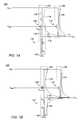
- the voltage regulator 100includes a reference leg 102 coupled between a voltage source (V pwr ) and ground 104 , and an output leg 106 coupled between V pwr and an output node (V out ).
- the reference leg 102includes a first transistor 108 connected as a source follower (SF) and including a gate node (V gate ) coupled to and controlled by for example an operational amplifier or a charge pump (not shown) in the voltage regulator 100 , and an output node (V source ) coupled to ground 104 through a series resistor network 110 .
- the output leg 106includes a second larger transistor 112 , also connected as a source follower and controlled by the gate node (V gate ) of the first transistor 108 .
- the voltage regulator 100further includes a small feedback resistor (R f 114 ) coupling the output nodes of the first transistor 108 (V source ) and the second transistor 112 (V out ) to improve the accuracy and stability of the regulator.
- the first and the second transistors 108 , 112are selected so that the output voltage V out is a replica of the V source voltage.
- a ratio between resistors R 1 and R 2 in the series resistor network 110is selected so that V source is equal to the desired target voltage—that is it is the same as the desired V out .
- V pwris greater than V out and current flows through the reference leg 102 , indicated by arrows 116 , generating the desired target voltage at the output node of the first transistor 108 (V source ), which is then replicated at the output node of the second transistor 112 (V out ).
- Currentindicated by arrows 118 and 120 , flows from the sources (V source and V out ) of the first and the second transistors 108 , 112 to the output node (V out ) of the voltage regulator 100 .
- the present inventionprovides a solution to these and other problems, and offers further advantages over conventional voltage regulators and methods of operating the same.
- the present inventionis directed to a circuit for interrupting current flow into a voltage regulator from an output of the voltage regulator.
- the circuitcomprises: (i) a comparator including an output, an input coupled to a voltage source, and an input coupled to the output of the voltage regulator; and (ii) a number of transistors coupled to the output of the comparator and controlled thereby.
- the number of transistorsinclude a first transistor configured to interrupt a first current path extending between the output of the voltage regulator and the voltage source through an output leg of the voltage regulator when a voltage of the voltage source (V pwr ) drops below a voltage at the output of the voltage regulator (V out ).
- the comparatoris powered by the output of the voltage regulator (V out ) rather than the voltage source (V pwr ) to avoid a varying or dropping V pwr from adversely effecting operation of the comparator.
- the voltage regulatoris a replica voltage regulator further including a reference leg and a feedback circuit coupling V out to the reference leg, and the first transistor is also configured to interrupt a second current path extending between the output of the voltage regulator and the voltage source through the feedback circuit and at least partially through reference leg.
- the reference legfurther includes a resistor network through which the feedback circuit is coupled to a circuit ground, and the number of transistors include a second transistor configured to interrupt a third current path extending between the output of the voltage regulator and circuit ground through the feedback circuit and the resistor network when V pwr drops below V out .
- the output legincludes a first source follower (SF) transistor in the first current path and the reference leg includes a second SF transistor in the second current path, and the first transistor is configured to pull gate nodes of the first and second SF transistors to a circuit ground when V pwr drops below V out .
- SFsource follower
- the comparatoris also configured to signal a device comprising or coupled to the voltage regulator when V pwr drops below V out .
- the present inventionis directed to a method of operating a voltage regulator to interrupt current flow into the voltage regulator from an output thereof.
- the methodincluding steps of: (i) a comparing V pwr of a voltage source coupled to the voltage regulator to V out at the output of the voltage regulator; and (ii) controlling a number of transistors to substantially prevent current from flowing from the output of the voltage regulator into the voltage regulator when V pwr drops below V out .
- the voltage regulatoris a replica voltage regulator comprising a reference leg and an output leg, and the method includes the step of interrupting a first current path extending between the output of the voltage regulator and the voltage source through an output leg of the voltage regulator when V pwr drops below V out .
- the voltage regulatorfurther comprises a feedback circuit coupling V out to the reference leg, and wherein the method further includes the step of interrupting a second current path extending between the output of the voltage regulator and the voltage source through the feedback circuit and at least partially through reference leg when V pwr drops below V out .
- the output legcomprises a first SF transistor in the first current path and the reference leg comprises a second SF transistor in the first current path
- the steps of interrupting the first and second current pathsinclude the steps of pulling gate nodes of the first and second SF transistors to a circuit ground when V pwr drops below V out
- the reference legfurther comprises a resistor network through which the feedback circuit is coupled to circuit ground
- the methodfurther includes the step of interrupting a third current path extending between the output of the voltage regulator and circuit ground through the feedback circuit and the resistor network when V pwr drops below V out .
- the methodcan further include the step of signaling a device comprising or coupled to the voltage regulator when V pwr drops below V out .
- FIG. 1Ais a simplified schematic diagram illustrating current flow in an output stage of a voltage regulator when a power supply is greater than the output voltage for which a circuit and method of the present invention is particularly useful;
- FIG. 1Bis a simplified schematic diagram of the voltage regulator of FIG. 1A illustrating current flow into the voltage regulator when a power supply voltage drops below an output voltage;
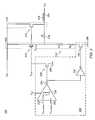
- FIG. 2is a schematic diagram an output stage of a voltage regulator including a circuit to substantially prevent or interrupt reverse current flow into the voltage regulator from an output thereof according to an embodiment of the present invention
- FIG. 3is a flowchart of a method according to an embodiment of the present invention for operating a voltage regulator to substantially prevent or interrupt reverse current flow into the voltage regulator from an output thereof;
- FIG. 4are graphs illustrating the ability of a circuit according to the present invention to substantially prevent or interrupt reverse current flow into the voltage regulator from an output thereof.
- the present inventionis directed to a circuit and method for interrupting or substantially preventing reverse current flow into an output of a voltage regulator when a voltage of a voltage source of the voltage regulator drops below a voltage at the output of the voltage regulator.
- the voltage regulator and method of the present inventionare particularly useful in battery operated devices, such as a wireless computer mouse and other like devices, which include integrated voltage regulators.
- the circuit of the present inventionincludes a comparator including an output, an input coupled to a voltage source, and an input coupled to the output of the voltage regulator, and a number of transistors coupled to the output of the comparator to interrupt or substantially prevent current from flowing from the output of the voltage regulator into the voltage regulator when a voltage of a voltage source (V pwr ) of the voltage regulator drops below a voltage at the output of the voltage regulator (V out ).
- a comparatorincluding an output, an input coupled to a voltage source, and an input coupled to the output of the voltage regulator, and a number of transistors coupled to the output of the comparator to interrupt or substantially prevent current from flowing from the output of the voltage regulator into the voltage regulator when a voltage of a voltage source (V pwr ) of the voltage regulator drops below a voltage at the output of the voltage regulator (V out ).
- FIG. 2shows a schematic view of an output stage of a voltage regulator 200 including an interrupt circuit or circuit 202 for interrupting or substantially preventing reverse current flow into an output 204 of the regulator when V pwr drops below V out according to an embodiment of the present invention.
- an interrupt circuit or circuit 202for interrupting or substantially preventing reverse current flow into an output 204 of the regulator when V pwr drops below V out according to an embodiment of the present invention.
- ICintegrated circuit
- the voltage regulator 200is a replica type voltage regulator and includes a reference leg 206 coupled between V pwr and ground 208 , and an output leg 210 coupled between V pwr and the output node 204 .
- the reference leg 206includes a first transistor 212 connected as a source follower (SF) and including a gate node (V gate ) coupled to and controlled by an operational amplifier (OPAMP) or a charge pump and an output node (V source ) coupled to ground 208 through a series resistor network 214 .
- the output leg 210includes a second larger transistor 216 , also connected as a source follower and controlled by the gate node (V gate ) of the first transistor 212 .
- the voltage regulator 200further includes a small a feedback resistor (R f 218 ) coupling the output nodes of the first transistor 212 (V source ) and the second transistor 216 (V out ) to improve the accuracy and stability of the regulator.
- the first and the second transistors 212 , 216are selected so that the output voltage V out is a replica of the V source voltage.
- a ratio between resistors R 1 and R 2 in the series resistor network 214is selected so that V source is equal to the desired target voltage—that is it is the same as the desired V out .
- In normal operation current, indicated by arrow 219flows from the sources of the first and the second transistors 212 , 216 to the output node 204 of the voltage regulator 200 .
- the interrupt circuit 202comprises a comparator 220 powered by the output node 204 (V out ) and including a non-inverting input 222 coupled to a filtered voltage from the voltage source (V pwr — filtered ) and an inverting input 224 coupled to a filtered voltage from the output of the voltage regulator (V out — filtered ).
- filtered voltageit is meant the voltage is processed to attenuate or remove completely in unwanted variation or ripple in the voltage applied to the filter. Filtering can be accomplished by any known filter circuit (not shown) including, for example, an active or passive filter, such as a RC-filter.
- the comparator 220further includes an output 226 coupled to a number of transistors configured or adapted to substantially prevent current from flowing from the output 204 into the voltage regulator 200 when V pwr drops below V out .
- the number of transistorsinclude a first transistor 228 configured to interrupt a first and second current paths extending between the output 204 of the voltage regulator 200 and the voltage source through the reference leg 206 and output leg 210 when V pwr drops below V out .
- the first transistoris a leaker transistor configured to pull gate nodes of the first and second SF transistors 212 , 216 to ground 208 when V pwr drops below V out .
- the number of transistorsinclude an inverter 232 and a second, normally closed switching transistor 230 configured to interrupt a third current path extending between the output 204 of the voltage regulator 200 and circuit ground through the feedback resistor 218 and the resistor network 214 when V pwr drops below V out .
- FIG. 3is a flowchart of a method according to an embodiment of the present invention for operating a voltage regulator to interrupt current flow into the voltage regulator from an output thereof.
- the methodbegins with comparing V pwr of a voltage source coupled to the voltage regulator to V out at the output of the voltage regulator (step 302 ).
- a leaker transistoris controlled or operated to couple or pull a gate node of a first SF transistor in an output leg of the voltage regulator to a circuit ground when V pwr drops below V out (step 304 ).
- the leaker transistoris also operated to pull a gate node of a second SF transistor in a reference leg of the voltage regulator to circuit ground when V pwr drops below V out (step 306 ).
- a switching transistoris operated to open a current path coupling the reference leg to circuit ground when V pwr drops below V out (step 308 ).
- the steps of pulling gate nodes of the first and second SF transistors to ground, step 304 and 306 respectively, and operating the switching transistor, step 308are performed at substantially the same time.
- the switching transistoris in connected in series with a resistor network in the reference leg.
- the methodcan further include the step of signaling a device comprising or coupled to the voltage regulator when V pwr drops below V out (step 310 ). More preferably, the signaling step, step 310 , is performed at substantially the same time as steps 304 , 306 and 308 .
- FIG. 4includes four separate graphs illustrating exemplary inputs to and outputs from the circuits of FIG. 2 .
- Line 402 in the top graphlabeled V pwr and V out (V) illustrates a voltage of the voltage source (V pwr ) and line 404 the voltage at the output of the voltage regulator (V out ).
- Line 406 in the second graph from the toplabeled Comparator output (V), illustrates a change in the output of the comparator (comparator 220 in FIG.
- Line 408 in the third graphlabeled Gate of SF (V) illustrates a voltage to the gate nodes of the first and second source followers (transistors 228 and 230 in FIG. 2 ).
- V pwrline 402
- the comparator outputline 406
- the voltage applied to the gate nodes of the first and second source followersline 408
- V pwrthe voltage applied to the gate nodes of the first and second source followers
- V pwr(line 402 ) continues to droop and at about T equal 1.132 mS drops below V out (line 404 ).
- the comparator output(line 406 ) goes high to about 3V operating the leaker transistors (transistor 228 in FIG. 2 ) to couple the gate nodes of the first and second source followers (line 408 ) to ground.
- line 410 in the bottom graphcurrent flow out of the voltage regulator quickly settles at about 0 mA at T 1.14 mS after a brief dip (reverse current flow) indicated by dashed line 412 peaking at less than about ⁇ 0.6 mA.
- the advantages of the circuit and method of the present invention over previous or conventional systems and methodsinclude: (i) interrupting or substantially preventing reverse current flowing into the voltage regulator when V pwr drops below V out ; (ii) substantially preventing any voltage drop or droop in the output voltage when V pwr drops below V out ; (iii) ability to signal a device comprising or coupled to the voltage regulator when V pwr drops below V out ; (iv) increasing battery life time in battery operated devices, such as a wireless computer mouse and other like devices, by interrupting or substantially preventing reverse current flowing into the voltage regulator, which can quickly drain the battery; and (v) having substantially no impact on the performance of the voltage regulator in normal operating mode.
Landscapes
- Engineering & Computer Science (AREA)
- Physics & Mathematics (AREA)
- Electromagnetism (AREA)
- General Physics & Mathematics (AREA)
- Radar, Positioning & Navigation (AREA)
- Automation & Control Theory (AREA)
- Continuous-Control Power Sources That Use Transistors (AREA)
Abstract
Description
Claims (20)
Priority Applications (1)
| Application Number | Priority Date | Filing Date | Title |
|---|---|---|---|
| US12/009,877US7859240B1 (en) | 2007-05-22 | 2008-01-22 | Circuit and method for preventing reverse current flow into a voltage regulator from an output thereof |
Applications Claiming Priority (2)
| Application Number | Priority Date | Filing Date | Title |
|---|---|---|---|
| US93121607P | 2007-05-22 | 2007-05-22 | |
| US12/009,877US7859240B1 (en) | 2007-05-22 | 2008-01-22 | Circuit and method for preventing reverse current flow into a voltage regulator from an output thereof |
Publications (1)
| Publication Number | Publication Date |
|---|---|
| US7859240B1true US7859240B1 (en) | 2010-12-28 |
Family
ID=43357342
Family Applications (2)
| Application Number | Title | Priority Date | Filing Date |
|---|---|---|---|
| US12/009,877Active2029-01-31US7859240B1 (en) | 2007-05-22 | 2008-01-22 | Circuit and method for preventing reverse current flow into a voltage regulator from an output thereof |
| US12/154,169Active2029-10-26US8080984B1 (en) | 2007-05-22 | 2008-05-21 | Replica transistor voltage regulator |
Family Applications After (1)
| Application Number | Title | Priority Date | Filing Date |
|---|---|---|---|
| US12/154,169Active2029-10-26US8080984B1 (en) | 2007-05-22 | 2008-05-21 | Replica transistor voltage regulator |
Country Status (1)
| Country | Link |
|---|---|
| US (2) | US7859240B1 (en) |
Cited By (3)
| Publication number | Priority date | Publication date | Assignee | Title |
|---|---|---|---|---|
| US9582017B2 (en) | 2013-07-02 | 2017-02-28 | Stmicroelectronics Design And Application S.R.O. | Method of preventing inversion of output current flow in a voltage regulator and related voltage regulator |
| US10630028B2 (en) | 2018-04-12 | 2020-04-21 | Cypress Semiconductor Corporation | Reverse overcurrent protection for universal serial bus type-C (USB-C) connector systems |
| US10763661B2 (en) | 2016-10-10 | 2020-09-01 | Nxp B.V. | Reverse current protection circuit for switch circuit |
Families Citing this family (20)
| Publication number | Priority date | Publication date | Assignee | Title |
|---|---|---|---|---|
| US8378654B2 (en) | 2009-04-01 | 2013-02-19 | Taiwan Semiconductor Manufacturing Company, Ltd. | Voltage regulator with high accuracy and high power supply rejection ratio |
| US8598854B2 (en)* | 2009-10-20 | 2013-12-03 | Taiwan Semiconductor Manufacturing Company, Ltd. | LDO regulators for integrated applications |
| US20110133719A1 (en)* | 2009-12-04 | 2011-06-09 | Advance Micro Devices, Inc. | Voltage reference circuit operable with a low voltage supply and method for implementing same |
| US8351886B1 (en)* | 2010-02-04 | 2013-01-08 | Triquint Semiconductor, Inc. | Voltage regulator with a bandwidth variation reduction network |
| US8378658B2 (en)* | 2010-06-25 | 2013-02-19 | Micrel, Inc. | Load swtch for removing high frequency ripple, noise and/or spikes while providing power to subsystems |
| US9059698B2 (en)* | 2010-10-11 | 2015-06-16 | Samsung Electronics Co., Ltd. | Integrated circuit devices using power supply circuits with feedback from a replica load |
| KR101153651B1 (en)* | 2010-12-30 | 2012-06-18 | 삼성전기주식회사 | Voltage regulator with multiple output |
| US9874887B2 (en)* | 2012-02-24 | 2018-01-23 | Silicon Laboratories Inc. | Voltage regulator with adjustable feedback |
| US9046905B2 (en) | 2013-03-08 | 2015-06-02 | Analog Devices Global | Apparatus and methods for bidirectional current sensing in a switching regulator |
| US8937467B2 (en)* | 2013-03-08 | 2015-01-20 | Analog Devices Technology | Apparatus and methods for switching regulator current sensing |
| US9461539B2 (en) | 2013-03-15 | 2016-10-04 | Taiwan Semiconductor Manufacturing Company, Ltd. | Self-calibrated voltage regulator |
| US9791480B2 (en) | 2013-05-21 | 2017-10-17 | Analog Devices Global | Current sensing of switching power regulators |
| CN104793673A (en)* | 2014-01-22 | 2015-07-22 | 上海华虹集成电路有限责任公司 | LDO circuit applied to HSIC connector whole chip integration |
| CN105652942A (en)* | 2016-03-15 | 2016-06-08 | 西安紫光国芯半导体有限公司 | Voltage drop reduction device |
| US10250139B2 (en)* | 2016-03-31 | 2019-04-02 | Micron Technology, Inc. | Apparatuses and methods for a load current control circuit for a source follower voltage regulator |
| US10461629B2 (en)* | 2018-02-19 | 2019-10-29 | Texas Instruments Incorporated | System and apparatus to provide current compensation |
| US10866606B2 (en)* | 2018-03-28 | 2020-12-15 | Qualcomm Incorporated | Methods and apparatuses for multiple-mode low drop out regulators |
| US11671081B2 (en)* | 2019-12-13 | 2023-06-06 | Qualcomm Incorporated | Rail-to-rail source follower buffer for switching regulator driver supply |
| US11625057B2 (en)* | 2021-03-04 | 2023-04-11 | United Semiconductor Japan Co., Ltd. | Voltage regulator providing quick response to load change |
| US11616505B1 (en)* | 2022-02-17 | 2023-03-28 | Qualcomm Incorporated | Temperature-compensated low-pass filter |
Citations (77)
| Publication number | Priority date | Publication date | Assignee | Title |
|---|---|---|---|---|
| US4158804A (en) | 1977-08-10 | 1979-06-19 | General Electric Company | MOSFET Reference voltage circuit |
| US4477737A (en) | 1982-07-14 | 1984-10-16 | Motorola, Inc. | Voltage generator circuit having compensation for process and temperature variation |
| US4689733A (en) | 1984-07-04 | 1987-08-25 | Bbc Brown, Boveri & Company, Limited | Method for reducing dynamic overvoltages in an alternating-current system to which a direct-current system is connected |
| US4829203A (en) | 1988-04-20 | 1989-05-09 | Texas Instruments Incorporated | Integrated programmable bit circuit with minimal power requirement |
| US4851759A (en) | 1988-05-26 | 1989-07-25 | North American Philips Corporation, Signetics Division | Unity-gain current-limiting circuit |
| US4866606A (en) | 1984-06-22 | 1989-09-12 | Austria Miktosystem International Gmbh | Loosely coupled distributed computer system with node synchronization for precision in real time applications |
| US4884161A (en) | 1983-05-26 | 1989-11-28 | Honeywell, Inc. | Integrated circuit voltage regulator with transient protection |
| US4885719A (en) | 1987-08-19 | 1989-12-05 | Ict International Cmos Technology, Inc. | Improved logic cell array using CMOS E2 PROM cells |
| US4890222A (en) | 1984-12-17 | 1989-12-26 | Honeywell Inc. | Apparatus for substantially syncronizing the timing subsystems of the physical modules of a local area network |
| US4893030A (en) | 1986-12-04 | 1990-01-09 | Western Digital Corporation | Biasing circuit for generating precise currents in an integrated circuit |
| US4897774A (en) | 1985-10-01 | 1990-01-30 | Maxim Integrated Products | Integrated dual charge pump power supply and RS-232 transmitter/receiver |
| US4935644A (en) | 1987-08-13 | 1990-06-19 | Kabushiki Kaisha Toshiba | Charge pump circuit having a boosted output signal |
| US5059815A (en) | 1990-04-05 | 1991-10-22 | Advanced Micro Devices, Inc. | High voltage charge pumps with series capacitors |
| US5087834A (en) | 1990-03-12 | 1992-02-11 | Texas Instruments Incorporated | Buffer circuit including comparison of voltage-shifted references |
| US5276646A (en) | 1990-09-25 | 1994-01-04 | Samsung Electronics Co., Ltd. | High voltage generating circuit for a semiconductor memory circuit |
| US5280233A (en) | 1991-02-27 | 1994-01-18 | Sgs-Thomson Microelectronics, S.R.L. | Low-drop voltage regulator |
| US5311480A (en) | 1992-12-16 | 1994-05-10 | Texas Instruments Incorporated | Method and apparatus for EEPROM negative voltage wordline decoding |
| US5319604A (en) | 1990-05-08 | 1994-06-07 | Texas Instruments Incorporated | Circuitry and method for selectively switching negative voltages in CMOS integrated circuits |
| US5371705A (en) | 1992-05-25 | 1994-12-06 | Mitsubishi Denki Kabushiki Kaisha | Internal voltage generator for a non-volatile semiconductor memory device |
| US5388249A (en) | 1987-04-27 | 1995-02-07 | Hitachi, Ltd. | Data processing system generating clock signal from an input clock, phase locked to the input clock and used for clocking logic devices |
| US5392421A (en) | 1989-04-25 | 1995-02-21 | Lennartsson; Kent | System for synchronizing clocks between communication units by using data from a synchronization message which competes with other messages for transfers over a common communication channel |
| US5402394A (en) | 1991-12-04 | 1995-03-28 | Turski; Klaus | Process for generating a common time base for a system with distributed computing units |
| US5438542A (en) | 1993-05-28 | 1995-08-01 | Kabushiki Kaisha Toshiba | Nonvolatile semiconductor memory device |
| US5461723A (en) | 1990-04-05 | 1995-10-24 | Mit Technology Corp. | Dual channel data block transfer bus |
| US5461557A (en) | 1992-09-02 | 1995-10-24 | Nec Corporation | Voltage converting circuit and multiphase clock generating circuit used for driving the same |
| US5570043A (en) | 1995-01-31 | 1996-10-29 | Cypress Semiconductor Corporation | Overvoltage tolerant intergrated circuit output buffer |
| US5587603A (en) | 1995-01-06 | 1996-12-24 | Actel Corporation | Two-transistor zero-power electrically-alterable non-volatile latch |
| US5592430A (en) | 1994-11-04 | 1997-01-07 | Nec Corporation | Semiconductor device equipped with simple stable switching circuit for selectively supplying different power voltages |
| US5600551A (en) | 1995-08-02 | 1997-02-04 | Schenck-Accurate, Inc. | Isolated power/voltage multiplier apparatus and method |
| US5621902A (en) | 1994-11-30 | 1997-04-15 | International Business Machines Corporation | Computer system having a bridge between two buses with a direct memory access controller and an alternative memory access controller |
| US5628001A (en) | 1992-11-23 | 1997-05-06 | Motorola, Inc. | Power saving method and apparatus for changing the frequency of a clock in response to a start signal |
| US5630147A (en) | 1993-12-17 | 1997-05-13 | Intel Corporation | System management shadow port |
| US5635872A (en) | 1995-11-16 | 1997-06-03 | Maven Peal Instruments, Inc. | Variable control of electronic power supplies |
| US5637992A (en) | 1995-05-31 | 1997-06-10 | Sgs-Thomson Microelectronics, Inc. | Voltage regulator with load pole stabilization |
| US5642489A (en) | 1994-12-19 | 1997-06-24 | International Business Machines Corporation | Bridge between two buses of a computer system with a direct memory access controller with accessible registers to support power management |
| US5666069A (en) | 1995-12-22 | 1997-09-09 | Cypress Semiconductor Corp. | Data output stage incorporating an inverting operational amplifier |
| US5675813A (en) | 1995-10-26 | 1997-10-07 | Microsoft Corporation | System and method for power control in a universal serial bus |
| US5691654A (en) | 1995-12-14 | 1997-11-25 | Cypress Semiconductor Corp. | Voltage level translator circuit |
| US5701272A (en) | 1995-06-07 | 1997-12-23 | Intel Corporation | Negative voltage switching circuit |
| US5740106A (en) | 1995-06-29 | 1998-04-14 | Cypress Semiconductor Corp. | Apparatus and method for nonvolatile configuration circuit |
| US5748923A (en) | 1994-03-14 | 1998-05-05 | Robert Bosch Gmbh | Method for the cyclic transmission of data between at least two control devices with distributed operation |
| US5748911A (en) | 1996-07-19 | 1998-05-05 | Compaq Computer Corporation | Serial bus system for shadowing registers |
| US5754799A (en) | 1996-02-28 | 1998-05-19 | Paradyne Corporation | System and method for bus contention resolution |
| US5757228A (en) | 1992-11-04 | 1998-05-26 | Mitsubishi Denki Kabushiki Kaisha | Output driver circuit for suppressing noise generation and integrated circuit device for burn-in test |
| US5761058A (en) | 1995-07-26 | 1998-06-02 | Matsushita Electric Works, Ltd. | Power converter apparatus for a discharge lamp |
| US5767844A (en) | 1996-02-29 | 1998-06-16 | Sun Microsystems Inc | Modified universal serial bus interface implementing remote power up while permitting normal remote power down |
| US5767735A (en) | 1995-09-29 | 1998-06-16 | Intel Corporation | Variable stage charge pump |
| US5774744A (en) | 1996-04-08 | 1998-06-30 | Vlsi Technology, Inc. | System using DMA and descriptor for implementing peripheral device bus mastering via a universal serial bus controller or an infrared data association controller |
| US5778218A (en) | 1996-12-19 | 1998-07-07 | Advanced Micro Devices, Inc. | Method and apparatus for clock synchronization across an isochronous bus by adjustment of frame clock rates |
| US5781028A (en) | 1996-06-21 | 1998-07-14 | Microsoft Corporation | System and method for a switched data bus termination |
| US5796656A (en) | 1997-02-22 | 1998-08-18 | Programmable Microelectronics Corporation | Row decoder circuit for PMOS non-volatile memory cell which uses electron tunneling for programming and erasing |
| US5812459A (en) | 1991-07-25 | 1998-09-22 | Kabushiki Kaisha Toshiba | Nonvolatile semiconductor memory device having row decoder supplying a negative potential to wordlines during erase mode |
| US5841696A (en) | 1997-03-05 | 1998-11-24 | Advanced Micro Devices, Inc. | Non-volatile memory enabling simultaneous reading and writing by time multiplexing a decode path |
| US5847993A (en) | 1997-06-23 | 1998-12-08 | Xilinx, Inc. | Non-volatile programmable CMOS logic cell and method of operating same |
| US5852370A (en) | 1994-12-22 | 1998-12-22 | Texas Instruments Incorporated | Integrated circuits for low power dissipation in signaling between different-voltage on chip regions |
| US5867013A (en) | 1997-11-20 | 1999-02-02 | Cypress Semiconductor Corporation | Startup circuit for band-gap reference circuit |
| US5871368A (en) | 1996-11-19 | 1999-02-16 | Intel Corporation | Bus connector |
| US5884086A (en) | 1997-04-15 | 1999-03-16 | International Business Machines Corporation | System and method for voltage switching to supply various voltages and power levels to a peripheral device |
| US5889664A (en) | 1996-08-21 | 1999-03-30 | Hyundai Electronics Industries Co., Ltd. | Multiple level voltage generator for semiconductor memory device |
| US5929692A (en) | 1997-07-11 | 1999-07-27 | Computer Products Inc. | Ripple cancellation circuit with fast load response for switch mode voltage regulators with synchronous rectification |
| US5938770A (en) | 1996-07-19 | 1999-08-17 | Samsung Electronics Co., Ltd. | Display apparatus for computer system |
| US5982158A (en) | 1999-04-19 | 1999-11-09 | Delco Electronics Corporaiton | Smart IC power control |
| US6025701A (en) | 1995-05-09 | 2000-02-15 | Siemens Aktiengesellschaft | Static and dynamic mains voltage support by a static power factor correction device having a self-commutated converter |
| US6094095A (en) | 1998-06-29 | 2000-07-25 | Cypress Semiconductor Corp. | Efficient pump for generating voltages above and/or below operating voltages |
| US6105097A (en) | 1998-10-14 | 2000-08-15 | Cypress Semiconductor Corp. | Device and method for interconnecting universal serial buses including power management |
| US6118676A (en) | 1998-11-06 | 2000-09-12 | Soft Switching Technologies Corp. | Dynamic voltage sag correction |
| US6144580A (en) | 1998-12-11 | 2000-11-07 | Cypress Semiconductor Corp. | Non-volatile inverter latch |
| US6157178A (en) | 1998-05-19 | 2000-12-05 | Cypress Semiconductor Corp. | Voltage conversion/regulator circuit and method |
| US6157176A (en) | 1997-07-14 | 2000-12-05 | Stmicroelectronics S.R.L. | Low power consumption linear voltage regulator having a fast response with respect to the load transients |
| US6222353B1 (en) | 2000-05-31 | 2001-04-24 | Philips Semiconductors, Inc. | Voltage regulator circuit |
| US6232757B1 (en) | 1999-08-20 | 2001-05-15 | Intel Corporation | Method for voltage regulation with supply noise rejection |
| US6373231B1 (en) | 2000-12-05 | 2002-04-16 | Cypress Semiconductor Corp. | Voltage regulator |
| US6522111B2 (en) | 2001-01-26 | 2003-02-18 | Linfinity Microelectronics | Linear voltage regulator using adaptive biasing |
| US6566851B1 (en) | 2000-08-10 | 2003-05-20 | Applied Micro Circuits, Corporation | Output conductance correction circuit for high compliance short-channel MOS switched current mirror |
| US6661214B1 (en) | 2001-09-28 | 2003-12-09 | Itt Manufacturing Enterprises, Inc. | Droop compensation circuitry |
| US6879142B2 (en) | 2003-08-20 | 2005-04-12 | Broadcom Corporation | Power management unit for use in portable applications |
| US7026802B2 (en) | 2003-12-23 | 2006-04-11 | Cypress Semiconductor Corporation | Replica biased voltage regulator |
Family Cites Families (10)
| Publication number | Priority date | Publication date | Assignee | Title |
|---|---|---|---|---|
| US5661395A (en) | 1995-09-28 | 1997-08-26 | International Business Machines Corporation | Active, low Vsd, field effect transistor current source |
| EP1115203B1 (en) | 1999-06-18 | 2006-11-08 | Matsushita Electric Industrial Co., Ltd. | Output controller |
| US6249177B1 (en) | 2000-09-28 | 2001-06-19 | Cypress Semiconductor Corp. | Method, circuit and/or architecture for reducing gate oxide stress in low-voltage regulated devices |
| US6601936B2 (en) | 2000-11-14 | 2003-08-05 | Cypress Semiconductor Corp. | Real time adaptive inkjet temperature regulation controller |
| US6441593B1 (en) | 2000-12-14 | 2002-08-27 | Cypress Semiconductor Corp. | Low noise switching regulator |
| US6501256B1 (en) | 2001-06-29 | 2002-12-31 | Intel Corporation | Trimmable bandgap voltage reference |
| US7002401B2 (en) | 2003-01-30 | 2006-02-21 | Sandisk Corporation | Voltage buffer for capacitive loads |
| GB2405707B (en) | 2003-09-05 | 2007-03-14 | Micron Technology Europ Ltd | Low voltage bandgap reference circuit with reduced area |
| US7106042B1 (en)* | 2003-12-05 | 2006-09-12 | Cypress Semiconductor Corporation | Replica bias regulator with sense-switched load regulation control |
| US7319314B1 (en)* | 2004-12-22 | 2008-01-15 | Cypress Semiconductor Corporation | Replica regulator with continuous output correction |
- 2008
- 2008-01-22USUS12/009,877patent/US7859240B1/enactiveActive
- 2008-05-21USUS12/154,169patent/US8080984B1/enactiveActive
Patent Citations (77)
| Publication number | Priority date | Publication date | Assignee | Title |
|---|---|---|---|---|
| US4158804A (en) | 1977-08-10 | 1979-06-19 | General Electric Company | MOSFET Reference voltage circuit |
| US4477737A (en) | 1982-07-14 | 1984-10-16 | Motorola, Inc. | Voltage generator circuit having compensation for process and temperature variation |
| US4884161A (en) | 1983-05-26 | 1989-11-28 | Honeywell, Inc. | Integrated circuit voltage regulator with transient protection |
| US4866606A (en) | 1984-06-22 | 1989-09-12 | Austria Miktosystem International Gmbh | Loosely coupled distributed computer system with node synchronization for precision in real time applications |
| US4689733A (en) | 1984-07-04 | 1987-08-25 | Bbc Brown, Boveri & Company, Limited | Method for reducing dynamic overvoltages in an alternating-current system to which a direct-current system is connected |
| US4890222A (en) | 1984-12-17 | 1989-12-26 | Honeywell Inc. | Apparatus for substantially syncronizing the timing subsystems of the physical modules of a local area network |
| US4897774A (en) | 1985-10-01 | 1990-01-30 | Maxim Integrated Products | Integrated dual charge pump power supply and RS-232 transmitter/receiver |
| US4893030A (en) | 1986-12-04 | 1990-01-09 | Western Digital Corporation | Biasing circuit for generating precise currents in an integrated circuit |
| US5388249A (en) | 1987-04-27 | 1995-02-07 | Hitachi, Ltd. | Data processing system generating clock signal from an input clock, phase locked to the input clock and used for clocking logic devices |
| US4935644A (en) | 1987-08-13 | 1990-06-19 | Kabushiki Kaisha Toshiba | Charge pump circuit having a boosted output signal |
| US4885719A (en) | 1987-08-19 | 1989-12-05 | Ict International Cmos Technology, Inc. | Improved logic cell array using CMOS E2 PROM cells |
| US4829203A (en) | 1988-04-20 | 1989-05-09 | Texas Instruments Incorporated | Integrated programmable bit circuit with minimal power requirement |
| US4851759A (en) | 1988-05-26 | 1989-07-25 | North American Philips Corporation, Signetics Division | Unity-gain current-limiting circuit |
| US5392421A (en) | 1989-04-25 | 1995-02-21 | Lennartsson; Kent | System for synchronizing clocks between communication units by using data from a synchronization message which competes with other messages for transfers over a common communication channel |
| US5087834A (en) | 1990-03-12 | 1992-02-11 | Texas Instruments Incorporated | Buffer circuit including comparison of voltage-shifted references |
| US5461723A (en) | 1990-04-05 | 1995-10-24 | Mit Technology Corp. | Dual channel data block transfer bus |
| US5059815A (en) | 1990-04-05 | 1991-10-22 | Advanced Micro Devices, Inc. | High voltage charge pumps with series capacitors |
| US5319604A (en) | 1990-05-08 | 1994-06-07 | Texas Instruments Incorporated | Circuitry and method for selectively switching negative voltages in CMOS integrated circuits |
| US5276646A (en) | 1990-09-25 | 1994-01-04 | Samsung Electronics Co., Ltd. | High voltage generating circuit for a semiconductor memory circuit |
| US5280233A (en) | 1991-02-27 | 1994-01-18 | Sgs-Thomson Microelectronics, S.R.L. | Low-drop voltage regulator |
| US5812459A (en) | 1991-07-25 | 1998-09-22 | Kabushiki Kaisha Toshiba | Nonvolatile semiconductor memory device having row decoder supplying a negative potential to wordlines during erase mode |
| US5402394A (en) | 1991-12-04 | 1995-03-28 | Turski; Klaus | Process for generating a common time base for a system with distributed computing units |
| US5371705A (en) | 1992-05-25 | 1994-12-06 | Mitsubishi Denki Kabushiki Kaisha | Internal voltage generator for a non-volatile semiconductor memory device |
| US5461557A (en) | 1992-09-02 | 1995-10-24 | Nec Corporation | Voltage converting circuit and multiphase clock generating circuit used for driving the same |
| US5757228A (en) | 1992-11-04 | 1998-05-26 | Mitsubishi Denki Kabushiki Kaisha | Output driver circuit for suppressing noise generation and integrated circuit device for burn-in test |
| US5628001A (en) | 1992-11-23 | 1997-05-06 | Motorola, Inc. | Power saving method and apparatus for changing the frequency of a clock in response to a start signal |
| US5311480A (en) | 1992-12-16 | 1994-05-10 | Texas Instruments Incorporated | Method and apparatus for EEPROM negative voltage wordline decoding |
| US5438542A (en) | 1993-05-28 | 1995-08-01 | Kabushiki Kaisha Toshiba | Nonvolatile semiconductor memory device |
| US5630147A (en) | 1993-12-17 | 1997-05-13 | Intel Corporation | System management shadow port |
| US5748923A (en) | 1994-03-14 | 1998-05-05 | Robert Bosch Gmbh | Method for the cyclic transmission of data between at least two control devices with distributed operation |
| US5592430A (en) | 1994-11-04 | 1997-01-07 | Nec Corporation | Semiconductor device equipped with simple stable switching circuit for selectively supplying different power voltages |
| US5621902A (en) | 1994-11-30 | 1997-04-15 | International Business Machines Corporation | Computer system having a bridge between two buses with a direct memory access controller and an alternative memory access controller |
| US5642489A (en) | 1994-12-19 | 1997-06-24 | International Business Machines Corporation | Bridge between two buses of a computer system with a direct memory access controller with accessible registers to support power management |
| US5852370A (en) | 1994-12-22 | 1998-12-22 | Texas Instruments Incorporated | Integrated circuits for low power dissipation in signaling between different-voltage on chip regions |
| US5587603A (en) | 1995-01-06 | 1996-12-24 | Actel Corporation | Two-transistor zero-power electrically-alterable non-volatile latch |
| US5570043A (en) | 1995-01-31 | 1996-10-29 | Cypress Semiconductor Corporation | Overvoltage tolerant intergrated circuit output buffer |
| US6025701A (en) | 1995-05-09 | 2000-02-15 | Siemens Aktiengesellschaft | Static and dynamic mains voltage support by a static power factor correction device having a self-commutated converter |
| US5637992A (en) | 1995-05-31 | 1997-06-10 | Sgs-Thomson Microelectronics, Inc. | Voltage regulator with load pole stabilization |
| US5701272A (en) | 1995-06-07 | 1997-12-23 | Intel Corporation | Negative voltage switching circuit |
| US5740106A (en) | 1995-06-29 | 1998-04-14 | Cypress Semiconductor Corp. | Apparatus and method for nonvolatile configuration circuit |
| US5761058A (en) | 1995-07-26 | 1998-06-02 | Matsushita Electric Works, Ltd. | Power converter apparatus for a discharge lamp |
| US5600551A (en) | 1995-08-02 | 1997-02-04 | Schenck-Accurate, Inc. | Isolated power/voltage multiplier apparatus and method |
| US5767735A (en) | 1995-09-29 | 1998-06-16 | Intel Corporation | Variable stage charge pump |
| US5675813A (en) | 1995-10-26 | 1997-10-07 | Microsoft Corporation | System and method for power control in a universal serial bus |
| US5635872A (en) | 1995-11-16 | 1997-06-03 | Maven Peal Instruments, Inc. | Variable control of electronic power supplies |
| US5691654A (en) | 1995-12-14 | 1997-11-25 | Cypress Semiconductor Corp. | Voltage level translator circuit |
| US5666069A (en) | 1995-12-22 | 1997-09-09 | Cypress Semiconductor Corp. | Data output stage incorporating an inverting operational amplifier |
| US5754799A (en) | 1996-02-28 | 1998-05-19 | Paradyne Corporation | System and method for bus contention resolution |
| US5767844A (en) | 1996-02-29 | 1998-06-16 | Sun Microsystems Inc | Modified universal serial bus interface implementing remote power up while permitting normal remote power down |
| US5774744A (en) | 1996-04-08 | 1998-06-30 | Vlsi Technology, Inc. | System using DMA and descriptor for implementing peripheral device bus mastering via a universal serial bus controller or an infrared data association controller |
| US5781028A (en) | 1996-06-21 | 1998-07-14 | Microsoft Corporation | System and method for a switched data bus termination |
| US5748911A (en) | 1996-07-19 | 1998-05-05 | Compaq Computer Corporation | Serial bus system for shadowing registers |
| US5938770A (en) | 1996-07-19 | 1999-08-17 | Samsung Electronics Co., Ltd. | Display apparatus for computer system |
| US5889664A (en) | 1996-08-21 | 1999-03-30 | Hyundai Electronics Industries Co., Ltd. | Multiple level voltage generator for semiconductor memory device |
| US5871368A (en) | 1996-11-19 | 1999-02-16 | Intel Corporation | Bus connector |
| US5778218A (en) | 1996-12-19 | 1998-07-07 | Advanced Micro Devices, Inc. | Method and apparatus for clock synchronization across an isochronous bus by adjustment of frame clock rates |
| US5796656A (en) | 1997-02-22 | 1998-08-18 | Programmable Microelectronics Corporation | Row decoder circuit for PMOS non-volatile memory cell which uses electron tunneling for programming and erasing |
| US5841696A (en) | 1997-03-05 | 1998-11-24 | Advanced Micro Devices, Inc. | Non-volatile memory enabling simultaneous reading and writing by time multiplexing a decode path |
| US5884086A (en) | 1997-04-15 | 1999-03-16 | International Business Machines Corporation | System and method for voltage switching to supply various voltages and power levels to a peripheral device |
| US5847993A (en) | 1997-06-23 | 1998-12-08 | Xilinx, Inc. | Non-volatile programmable CMOS logic cell and method of operating same |
| US5929692A (en) | 1997-07-11 | 1999-07-27 | Computer Products Inc. | Ripple cancellation circuit with fast load response for switch mode voltage regulators with synchronous rectification |
| US6157176A (en) | 1997-07-14 | 2000-12-05 | Stmicroelectronics S.R.L. | Low power consumption linear voltage regulator having a fast response with respect to the load transients |
| US5867013A (en) | 1997-11-20 | 1999-02-02 | Cypress Semiconductor Corporation | Startup circuit for band-gap reference circuit |
| US6157178A (en) | 1998-05-19 | 2000-12-05 | Cypress Semiconductor Corp. | Voltage conversion/regulator circuit and method |
| US6094095A (en) | 1998-06-29 | 2000-07-25 | Cypress Semiconductor Corp. | Efficient pump for generating voltages above and/or below operating voltages |
| US6105097A (en) | 1998-10-14 | 2000-08-15 | Cypress Semiconductor Corp. | Device and method for interconnecting universal serial buses including power management |
| US6118676A (en) | 1998-11-06 | 2000-09-12 | Soft Switching Technologies Corp. | Dynamic voltage sag correction |
| US6144580A (en) | 1998-12-11 | 2000-11-07 | Cypress Semiconductor Corp. | Non-volatile inverter latch |
| US5982158A (en) | 1999-04-19 | 1999-11-09 | Delco Electronics Corporaiton | Smart IC power control |
| US6232757B1 (en) | 1999-08-20 | 2001-05-15 | Intel Corporation | Method for voltage regulation with supply noise rejection |
| US6222353B1 (en) | 2000-05-31 | 2001-04-24 | Philips Semiconductors, Inc. | Voltage regulator circuit |
| US6566851B1 (en) | 2000-08-10 | 2003-05-20 | Applied Micro Circuits, Corporation | Output conductance correction circuit for high compliance short-channel MOS switched current mirror |
| US6373231B1 (en) | 2000-12-05 | 2002-04-16 | Cypress Semiconductor Corp. | Voltage regulator |
| US6522111B2 (en) | 2001-01-26 | 2003-02-18 | Linfinity Microelectronics | Linear voltage regulator using adaptive biasing |
| US6661214B1 (en) | 2001-09-28 | 2003-12-09 | Itt Manufacturing Enterprises, Inc. | Droop compensation circuitry |
| US6879142B2 (en) | 2003-08-20 | 2005-04-12 | Broadcom Corporation | Power management unit for use in portable applications |
| US7026802B2 (en) | 2003-12-23 | 2006-04-11 | Cypress Semiconductor Corporation | Replica biased voltage regulator |
Non-Patent Citations (21)
| Title |
|---|
| USPTO Final Rejection for Application No. 09/106,808 dated Dec. 3, 1999; 10 pages. |
| USPTO Non-Final Rejection for Application No. 08/577,258 dated Aug. 30, 1996; 11 pages. |
| USPTO Non-Final Rejection for Application No. 08/974,436 dated Apr. 30, 1998; 4 pages. |
| USPTO Non-Final Rejection for Application No. 09/106,808 dated Jun. 24, 1999; 8 pages. |
| USPTO Non-Final Rejection for Application No. 09/172,956 dated Dec. 20, 1999; 6 pages. |
| USPTO Non-Final Rejection for Application No. 09/276,321 dated Feb. 4, 2000; 3 pages. |
| USPTO Non-Final Rejection for U.S. Appl. No. 08/381,125 dated Jul. 11, 1995; 4 pages. |
| USPTO Non-Final Rejection for U.S. Appl. No. 08/381,125 dated Nov. 2, 1995; 5 pages. |
| USPTO Non-Final Rejection for U.S. Appl. No. 08/572,618 dated Sep. 18, 1996; 3 pages. |
| USPTO Non-Final Rejection for U.S. Appl. No. 09/730,315 dated May 23, 2001; 4 pages. |
| USPTO Non-Final Rejection for U.S. Appl. No. 10/965,445 dated May 3, 2005; 5 pages. |
| USPTO Notice of Allowance for Application No. 08/577,258 dated Apr. 24, 1997; 2 pages. |
| USPTO Notice of Allowance for Application No. 08/974,436 dated Aug. 3, 1998; 2 pages. |
| USPTO Notice of Allowance for Application No. 09/172,956 dated Apr. 6, 2000; 3 pages. |
| USPTO Notice of Allowance for Application No. 09/276,321 dated Jun. 12, 2000; 1 page. |
| USPTO Notice of Allowance for Application No. 09/456,801 dated Jun. 6, 2000; 3 pages. |
| USPTO Notice of Allowance for U.S. Appl. No. 08/381,125 dated May 1, 1996; 1 page. |
| USPTO Notice of Allowance for U.S. Appl. No. 08/572,618 dated Apr. 25, 1997; 1 page. |
| USPTO Notice of Allowance for U.S. Appl. No. 09/106,808 dated Mar. 21, 2000; 5 pages. |
| USPTO Notice of Allowance for U.S. Appl. No. 09/730,315 dated Nov. 20, 2001; 4 pages. |
| USPTO Notice of Allowance for U.S. Appl. No. 10/965,445 dated Oct. 26, 2005; 4 pages. |
Cited By (4)
| Publication number | Priority date | Publication date | Assignee | Title |
|---|---|---|---|---|
| US9582017B2 (en) | 2013-07-02 | 2017-02-28 | Stmicroelectronics Design And Application S.R.O. | Method of preventing inversion of output current flow in a voltage regulator and related voltage regulator |
| US10763661B2 (en) | 2016-10-10 | 2020-09-01 | Nxp B.V. | Reverse current protection circuit for switch circuit |
| US10630028B2 (en) | 2018-04-12 | 2020-04-21 | Cypress Semiconductor Corporation | Reverse overcurrent protection for universal serial bus type-C (USB-C) connector systems |
| US12040578B2 (en) | 2018-04-12 | 2024-07-16 | Cypress Semiconductor Corporation | Reverse overcurrent protection for Universal Serial Bus Type-C (USB-C) connector systems |
Also Published As
| Publication number | Publication date |
|---|---|
| US8080984B1 (en) | 2011-12-20 |
Similar Documents
| Publication | Publication Date | Title |
|---|---|---|
| US7859240B1 (en) | Circuit and method for preventing reverse current flow into a voltage regulator from an output thereof | |
| US8415935B2 (en) | Multiple branch alternative element power regulation | |
| US10481625B2 (en) | Voltage regulator | |
| US9214852B2 (en) | Precharge circuits and methods for DC-DC boost converters | |
| US9710002B2 (en) | Dynamic biasing circuits for low drop out (LDO) regulators | |
| JP6545692B2 (en) | Buffer circuit and method | |
| US11435768B2 (en) | N-channel input pair voltage regulator with soft start and current limitation circuitry | |
| US9484809B2 (en) | Apparatus and methods for low voltage high PSRR systems | |
| EP2120123A1 (en) | Slew rate control | |
| TWI639909B (en) | Voltage regulator | |
| JP4935585B2 (en) | Error amplification circuit and switching power supply circuit | |
| CN112925378A (en) | Quick response linear voltage regulator and quick response amplifying circuit thereof | |
| US20170364111A1 (en) | Linear voltage regulator | |
| US20180284826A1 (en) | Voltage regulator circuit, corresponding device, apparatus and method | |
| CN111490677A (en) | Adjusting tube driving circuit of charge pump with adjustable output voltage | |
| US12401210B2 (en) | Rectification by battery protection system | |
| TWI672572B (en) | Voltage Regulator | |
| US8111103B2 (en) | Amplifier circuit with overshoot suppression | |
| CN116185113A (en) | Soft start circuit, low dropout linear regulator, chip and electronic equipment | |
| JP2015050648A (en) | Backflow prevention switch and power supply device | |
| CN110024250B (en) | Circuit and method for managing inrush current | |
| JP4571215B2 (en) | Peak or zero current comparator | |
| US8129965B2 (en) | Quick-start low dropout regulator | |
| US11996715B2 (en) | Handling of battery loss event | |
| CN109474171B (en) | Control circuit and power management chip |
Legal Events
| Date | Code | Title | Description |
|---|---|---|---|
| AS | Assignment | Owner name:SILICON LIGHT MACHINES CORPORATION, CALIFORNIA Free format text:ASSIGNMENT OF ASSIGNORS INTEREST;ASSIGNORS:GEYNET, LIONEL;O'SULLIVAN, EUGENE;REEL/FRAME:020477/0436 Effective date:20080121 | |
| AS | Assignment | Owner name:CYPRESS SEMICONDUCTOR CORPORATION, CALIFORNIA Free format text:ASSIGNMENT OF ASSIGNORS INTEREST;ASSIGNOR:SILICON LIGHT MACHINES CORPORATION;REEL/FRAME:020908/0068 Effective date:20080417 | |
| STCF | Information on status: patent grant | Free format text:PATENTED CASE | |
| FPAY | Fee payment | Year of fee payment:4 | |
| AS | Assignment | Owner name:MORGAN STANLEY SENIOR FUNDING, INC., NEW YORK Free format text:SECURITY INTEREST;ASSIGNORS:CYPRESS SEMICONDUCTOR CORPORATION;SPANSION LLC;REEL/FRAME:035240/0429 Effective date:20150312 | |
| AS | Assignment | Owner name:CYPRESS SEMICONDUCTOR CORPORATION, CALIFORNIA Free format text:PARTIAL RELEASE OF SECURITY INTEREST IN PATENTS;ASSIGNOR:MORGAN STANLEY SENIOR FUNDING, INC., AS COLLATERAL AGENT;REEL/FRAME:039708/0001 Effective date:20160811 Owner name:SPANSION LLC, CALIFORNIA Free format text:PARTIAL RELEASE OF SECURITY INTEREST IN PATENTS;ASSIGNOR:MORGAN STANLEY SENIOR FUNDING, INC., AS COLLATERAL AGENT;REEL/FRAME:039708/0001 Effective date:20160811 | |
| FEPP | Fee payment procedure | Free format text:PAYOR NUMBER ASSIGNED (ORIGINAL EVENT CODE: ASPN); ENTITY STATUS OF PATENT OWNER: LARGE ENTITY | |
| AS | Assignment | Owner name:MONTEREY RESEARCH, LLC, CALIFORNIA Free format text:ASSIGNMENT OF ASSIGNORS INTEREST;ASSIGNOR:CYPRESS SEMICONDUCTOR CORPORATION;REEL/FRAME:040911/0238 Effective date:20160811 | |
| MAFP | Maintenance fee payment | Free format text:PAYMENT OF MAINTENANCE FEE, 8TH YEAR, LARGE ENTITY (ORIGINAL EVENT CODE: M1552) Year of fee payment:8 | |
| AS | Assignment | Owner name:MORGAN STANLEY SENIOR FUNDING, INC., NEW YORK Free format text:CORRECTIVE ASSIGNMENT TO CORRECT THE 8647899 PREVIOUSLY RECORDED ON REEL 035240 FRAME 0429. ASSIGNOR(S) HEREBY CONFIRMS THE SECURITY INTERST;ASSIGNORS:CYPRESS SEMICONDUCTOR CORPORATION;SPANSION LLC;REEL/FRAME:058002/0470 Effective date:20150312 | |
| MAFP | Maintenance fee payment | Free format text:PAYMENT OF MAINTENANCE FEE, 12TH YEAR, LARGE ENTITY (ORIGINAL EVENT CODE: M1553); ENTITY STATUS OF PATENT OWNER: LARGE ENTITY Year of fee payment:12 |