US7856577B2 - Command language for memory testing - Google Patents
Command language for memory testingDownload PDFInfo
- Publication number
- US7856577B2 US7856577B2US11/944,104US94410407AUS7856577B2US 7856577 B2US7856577 B2US 7856577B2US 94410407 AUS94410407 AUS 94410407AUS 7856577 B2US7856577 B2US 7856577B2
- Authority
- US
- United States
- Prior art keywords
- memory
- testing
- command
- compiled
- command interpreter
- Prior art date
- Legal status (The legal status is an assumption and is not a legal conclusion. Google has not performed a legal analysis and makes no representation as to the accuracy of the status listed.)
- Expired - Fee Related, expires
Links
Images


Classifications
- G—PHYSICS
- G06—COMPUTING OR CALCULATING; COUNTING
- G06F—ELECTRIC DIGITAL DATA PROCESSING
- G06F11/00—Error detection; Error correction; Monitoring
- G06F11/22—Detection or location of defective computer hardware by testing during standby operation or during idle time, e.g. start-up testing
- G06F11/26—Functional testing
- G06F11/27—Built-in tests
- G—PHYSICS
- G11—INFORMATION STORAGE
- G11C—STATIC STORES
- G11C29/00—Checking stores for correct operation ; Subsequent repair; Testing stores during standby or offline operation
- G11C29/04—Detection or location of defective memory elements, e.g. cell constructio details, timing of test signals
- G11C29/08—Functional testing, e.g. testing during refresh, power-on self testing [POST] or distributed testing
- G11C29/12—Built-in arrangements for testing, e.g. built-in self testing [BIST] or interconnection details
- G11C29/14—Implementation of control logic, e.g. test mode decoders
- G11C29/16—Implementation of control logic, e.g. test mode decoders using microprogrammed units, e.g. state machines
- G—PHYSICS
- G06—COMPUTING OR CALCULATING; COUNTING
- G06F—ELECTRIC DIGITAL DATA PROCESSING
- G06F8/00—Arrangements for software engineering
- G06F8/40—Transformation of program code
- G06F8/41—Compilation
Definitions
- the present disclosurerelates to memory devices and more particularly to the use of onboard computerized testing of memory devices.
- VLSIvery large scale integration
- One known testing methodis to incorporate a built-in memory test controller onto the VLSI chip.
- Such built-in memory test controllersutilize corresponding memory test algorithms to test memory circuits. While such devices have utility, as designs become larger and more complex, comprehensive testing often requires a number of different tests be run on memory circuits. As a result, built-in memory test controllers can become cumbersome as different types of tests are combined into the built-in controller.
- a memory testing systemfor testing a plurality of memory locations in an electronic memory device.
- the memory testing systemincludes a programmable memory device integrated into the electronic memory device capable of receiving and storing a compiled memory testing program.
- the testing systemfurther includes a processor in communication with the programmable memory device to read and execute instructions from the compiled testing program stored in the programmable memory device and a command interpreter configured to receive data from the processor related to commands to be executed during memory testing.
- a command language for use with a memory testing systemincludes a tangible memory storage device configured to store an indication of a memory program and a processor configured to access the memory storage device and executive instructions stored in the memory device for testing a plurality of memory locations on a memory device.
- the command languageincludes an instruction set including at least one command that, when executed, provides instruction to a command interpreter to access a memory location on the memory device.
- a method of testing a plurality of memory locations in an electronic memory device located on an integrated circuitincludes preparing and compiling a memory testing algorithm that, when executed, accesses at least one of the plurality of memory locations in the electronic memory device.
- the methodfurther includes storing the compiled memory testing algorithm on a programmable tangible storage medium located on the integrated circuit.
- the methodstill further includes accessing the compiled memory testing algorithm with a processor in communication with the tangible storage medium and executing the memory testing algorithm to test the plurality of memory locations.
- FIG. 1is a block diagram illustrating a memory testing system for testing an electronic memory device according to one illustrative embodiment.
- FIG. 2is a diagram illustrating various configurations of data packets provided to the command interpreter of FIG. 1 for interpretation to test memory devices.
- FIG. 3is an example of a testing program for use with the testing system of FIG. 1 .
- Memory testing systems and algorithmsare designed to determine whether memory locations are functioning properly. For example, a memory testing system may perform tests on memory locations to determine whether a known data pattern can be written to memory locations and then successfully read from the memory locations. As discussed above, as memory devices become more complex, onboard testing devices become more complex and cumbersome. Thus, the embodiments discussed herein are directed toward memory testing systems with an internal memory that are capable of having memory testing programs downloaded into them. The memory testing programs can then be read and interpreted, that is to say, executed, by a program reader that is external to the memory allocated for the memory testing system. The program reader is independent of the internal memory and thus is limited only by the capacity of the internal memory.
- MBISTMemory Built-In Self Test
- ARMAdvanced RISC Machine
- ARMAdvanced RISC Machine
- a personal testerthat employs, for example, a computing device with an input/output interface for accessing prototype circuit boards having memory devices that would benefit from memory testing.
- the memory testing systems described beloware advantageously adapted to be implemented on any number of different testing frameworks. The embodiments discussed below are thus capable of being implemented across a number of systems are not intended to be limited to the particular frameworks discussed below.
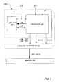
- FIG. 1illustrates a memory testing system 100 according to one illustrative embodiment.
- the memory testing system 100includes a processor 102 and a memory storage device 104 .
- Memory storage device 104includes memory locations for storage of a testing program.
- the processor 102is in communication with the memory storage device 104 so that processor 102 can read and/or write data from and/or to the memory storage device 104 .
- Address lines between the processor 102 and the memory storage device 104are identified as RA while data lines between the processor 102 and the memory storage device 104 are identified as DO. It should be appreciated that there may be any number of each of the RA address lines and the DO data lines as necessary to pass the appropriate data and address information between the processor 102 and the memory storage device 104 .
- Memory storage device 104can be any suitable type of memory storage. In one embodiment, the contents of memory storage device 104 can be rewritten to allow for the loading of any of a variety of testing programs that might be executed by the memory tester 100 .
- Processor 102is configured to access memory locations in memory storage device 104 to retrieve instructions and execute them. Testing programs that are loaded into the memory storage device 104 are precompiled so that at run time, the processor 102 merely accesses compiled commands and executes the program by executing the commands stored in the memory storage device 104 . Examples of a command language to be used with the memory testing system 100 is described in more detail below.
- a clock line CLKis provided to each of the processor 102 and memory storage device 104 to control the rate at which commands are executed. In one embodiment, the processor 102 executes one command per clock cycle.
- An enable line ENis also provided to the processor 102 and the memory storage device 104 . When the EN line is High, the processor 102 will retrieve and execute commands from the memory storage device 104 .
- the memory tester 100also includes a command interpreter 106 .
- the command interpreter 106is illustratively coupled to the processor 102 and receives signals from the processor, with which it interprets various commands.
- the processor 102provides information via one bit COM_TYPE and PA_TYPE lines, as well as via a plurality of DATA lines and a VALID status line.
- An IF lineprovided from the command interpreter 106 to the processor 102 provides status information to the processor 102 regarding the activities performed by the command interpreter 106 .
- Command interpreter 106is, in turn, in communication with memory 108 , which is the memory to be tested.
- the COM_TYPE and PAR_TYPE linesprovide information to the command interpreter 106 regarding how the information provided in the DATA lines should be interpreted.
- the VALID lineis provided to the command interpreter to indicate that the information on the COM_TYPE, PAR_TYPE, and DATA lines are valid.
- the VALID lineis illustratively equal
- the processor 102is adapted to execute commands from a command language designed for memory testing. The execution of these commands directs the processor to provide information to the command interpreter 106 on the lines described above. Below are exemplary commands for an embodiment of a command language.
- the LABEL(L)is an example of a non-executable command that associates a label L with a basic command following the label.
- the LOAD_JUMP commandthat illustratively includes a single parameter, L, which is a label that indicates a location in memory.
- the LOAD_JUMP commandsets the active jump label to L.
- the LOAD_JUMP(L)sets the PAR_TYPE line High and the COM_TYPE line Low. No action is performed by the command interpreter 106 upon execution of the LOAD_JUMP command.
- the SEND_COM(DATA) commandis an unconditional command that is executed by the processor 102 after which the processor 102 moves to the next basic command to be executed.
- the SEND_COM commandcauses the processor 102 to set the PAR_TYPE line Low and the COM_TYPE line Low and provides data on the DATA lines to the command interpreter 106 .
- the DATA parameterin one embodiment, is a seven-bit binary vector, with all seven bits used in code by the command interpreter 106 .
- the Low signals provided on each of the PAR_TYPE line and the COM_TYPE linecauses the command interpreter to parse the data provided by the DATA vector as follows:
- the described DATAis illustratively interpreted by the command interpreter 106 , which in turn executes meta commands to access and test memory locations in memory 108 .
- the command interpreter 106executes meta commands to access and test memory locations in memory 108 .
- the meta commandsthat the command interpreter 106 can execute along with a description of the commands.
- the command interpreter 106distinguishes between these commands by the values provided in the DATA vector from the controller 102 .
- a R(val) commandreads a two-bit value, val, from the current location in memory 108 .
- a W(val) commandwrites a two-bit value, val, to the current location in memory 108 .
- a W_MOVE(val,F) commandwrites a two-bit value, val, to the current location in memory 108 and moves forward to the next memory location as determined by the current memory route.
- the JUMP_IF — 0(L,DATA) commandis a conditional command that is executed by the processor 102 .
- the JUMP_IF — 0 commandhas two parameters: L, which is the label that points to a basic instruction and DATA, which is illustratively configured to be the same types of DATA passed to the command interpreter as described above related to the SEND_COM command.
- Lwhich is the label that points to a basic instruction
- DATAwhich is illustratively configured to be the same types of DATA passed to the command interpreter as described above related to the SEND_COM command.
- the JUMP_IF — 0illustratively is capable of instructing the command interpreter to perform the same types of commands (R(val), W(val), W_MOVE(val,F), and R_AND_JUMP(L,val)) as the SEND_COM command.
- the SEND_PAR(DATA) commandis a parameter setting command that is executed by the processor 102 after which the processor 102 moves to the next basic command to be executed.
- the SEND_PAR commandcauses the processor 102 to set the PAR_TYPE line High and the COM_TYPE line High and provides data on the DATA lines to the command interpreter 106 .
- the DATA parameterin one embodiment, is a seven-bit binary vector, with all seven bits used in code by the command interpreter.
- the SEND_PAR commandinstructs the command interpreter 106 to set various parameters by sending meta commands to the command interpreter 106 . Three exemplary types of meta commands are listed below and illustrated in FIG. 2 .
- a first exemplary type of meta commands associated with the SEND_PAR commandis a set_val type of commands 202 .
- the set_val commands 202have the following configuration for the seven-bit configuration for the DATA parameter:
- a first command of the set_val command typeis the set_enable_on command, which sets the value of the memory enable signal EN.
- the com_id for the set_enable_on commandis 0000.
- the memory enable lineis set to HIGH as is shown in command 210 .
- the memory enable lineis set to LOW as is shown in command 212 .
- the EN lineas is illustrated in FIG. 1 , provides a signal to cause the processor 102 and memory storage device 104 to execute commands.
- a second command of the set_val command typeis the set_cmp_on command, which enables or disables the comparison of memory output signals.
- the com_id for the set_cmp_on commandis 0001.
- a second exemplary type of meta commands associated with the SEND_PAR commandis a set_flags type of commands 220 .
- the set_flags commandshave the following configuration for the seven-bit configuration for the DATA parameter:
- a first command of the set_flags command type 220is the set_if_flag_to_last_adr command 226 .
- the set_if_flag_to_last_adr command 226selects the last_adr internal signal to be output through port IF.
- the value of the sel_flags variableis set to 00001.
- a second command of the set_flags command type 220is the set_if_flag_to_last_port command 228 .
- the set_if_flag_to_last_port commandsselects the last_port internal signal to be output through port IF.
- sel_flags00010.
- a third exemplary type of meta commands associated with the SEND_PAR commandis a set_pars type of commands 230 , which provide data to set different parameters.
- the set_pars commands 230have the following configuration for the seven-bit configuration for the DATA parameter:
- FIG. 3illustrates an example of a testing program 300 written as C code for a March type memory test algorithm.
- the programis 38 lines of nine-bit binary words.
- the nine bitsincludes the seven-bit DATA send to the command interpreter 106 , plus a two-bit prefix that codes the base executable commands (such as, for example, SEND_COM, LOAD_JUMP and any of the others described above) and to control command flow.
- a initialization portion 302 of the testing program 300illustratively defines arrays for use in the remainder of the program.
- the arraysinclude initial and target arrays having values for the initial and target states as well is information to determine the direction and dimension of traversal through the memory 108 .
- Variablesare assigned initial conditions for each of the initial and final states as well as the direction and dimension and passed to the command interpreter 106 .
- the EN lineis set to on and the active jump label is set.
- An initial writing portion 304 of the testing program 300assigns a label to a command that writes data to a location in memory and moves forward unless the IF line is 0.
- the initial writing portion 304then sets the comparison flag on, using command 214 .
- the labelis then assigned to a command to set the enable on, using the set_enable_on command.
- a loop portion 306 of the testing program 300performs a memory test by looping five times through a testing loop.
- different values for the init_state, target_state, direction, and dimensionare illustratively assigned from the arrays that were set up in the initialization portion 302 of the program. Once assigned, the values are passed to the command interpreter 106 using the set_oracle_par command 236 .
- the loop portionthen traverses the memory by first reading a value in a location and then writing a new value in that location, to be read during the next pass through the loop.
- testing program 300changes the active port and if the last port is not reached, loops back through the loop portion to test another portion of the memory 108 . If the last port has been reached, the testing program 300 exits the loop and terminates the program.
- testing programOnce the testing program has been written, it is illustratively compiled and loaded into the memory storage device 104 . Then, when it is advantageous to perform a memory test, a testing device such as one of the different types described above illustratively enables the processor 102 and the program is executed.
- the memory storage device 104is, in one embodiment, reprogrammable, so that the execution of a testing program such as testing program 300 can be performed, the memory storage device loaded with a different testing program and that program can be subsequently executed to perform another memory test on the same or different memory locations.
- the processor 102is capable of performing parallel testing of several memory instances.
- the embodiments discussed aboveprovide several important advantages. By creating a reprogrammable memory testing device that is locatable on board an integrated circuit device, the die size for the built-in testing solution is reduced. In addition, because a variety of different tests can be performed on chip merely by loading in a different testing program as opposed to using external testing devices, the tests can be performed more quickly, due to the increased speed capable by onboard testing devices. Further, testing of memory devices is extensible due to the lack of dedicated, custom design on board. Instead, testing programs can be changed on the fly during chip testing during manufacture verification testing.
Landscapes
- Engineering & Computer Science (AREA)
- General Engineering & Computer Science (AREA)
- Theoretical Computer Science (AREA)
- Computer Hardware Design (AREA)
- Quality & Reliability (AREA)
- Physics & Mathematics (AREA)
- General Physics & Mathematics (AREA)
- Tests Of Electronic Circuits (AREA)
Abstract
Description
- DATA=(e, A_kod, we, d).
The e variable is one-bit wide and is reserved for extra editing as needed. A_kod is a two-bit wide command for an address shuttle, which can more forward (F), backward (B) or stay at the same memory address in thememory 108. Addresses generated by the address shuttle are expanded in thememory 108 to the actual memory addresses that are to be read from or written to. The we variable is a two bit wide write enable signal. The we signal is expanded to the WRITE ENABLE memory input signal in thememory 108. The d variable is two-bits of data that is expanded in thememory 108 into data to be written to, or alternatively, read from memory.
- DATA=(e, A_kod, we, d).
- DATA=(set_id, com_id, val)
where setid is a two-bit identifier, which indicates the type of SEND_PAR command is being sent. In one embodiment, theset_id 204 for set_val commands202 is 11. Thecom_id 206 is a four-bit identifier to indicate which value is being set. Theval 208 is one bit of data to be set by the set_val command type. The following two commands are illustrative examples of set_val command types.
- DATA=(set_id, com_id, val)
- DATA=(set_id, sel_flags)
where the two-bit set_id 222 is illustratively designated as 10. Thesel_flags 224 is a five-bit vector that is to be used in a multiplexer module inside thecommand interpreter 106 to select a one-bit signal for the IF status line from up to 32 internal signals. The following two commands are illustrative examples of set_val command types.
- DATA=(set_id, sel_flags)
- DATA=(set_id, pars)
where the two-bit set_id 232 is illustratively designated as 00. The pars identifier234 is a six-bit vector that can be used to set internal parameters. One example of a set_pars command is theset_oracle_par command 236, which is used to set parameters describing the phase of a memory testing algorithm. Some examples of phases in the memory testing program include an init state and a target state, which code data patterns in memory before the start of the algorithm phase and after its completion. In addition, two parameters, dimension and direction indicate the direction that the memory testing algorithm traverses memory cells during a testing program, grouping memory into rows and columns. Examples of some types of paths that the memory testing algorithms including moving upward or downward, along rows or columns, or along a snake route.
- DATA=(set_id, pars)
Claims (18)
Priority Applications (1)
| Application Number | Priority Date | Filing Date | Title |
|---|---|---|---|
| US11/944,104US7856577B2 (en) | 2007-11-21 | 2007-11-21 | Command language for memory testing |
Applications Claiming Priority (1)
| Application Number | Priority Date | Filing Date | Title |
|---|---|---|---|
| US11/944,104US7856577B2 (en) | 2007-11-21 | 2007-11-21 | Command language for memory testing |
Publications (2)
| Publication Number | Publication Date |
|---|---|
| US20090133003A1 US20090133003A1 (en) | 2009-05-21 |
| US7856577B2true US7856577B2 (en) | 2010-12-21 |
Family
ID=40643317
Family Applications (1)
| Application Number | Title | Priority Date | Filing Date |
|---|---|---|---|
| US11/944,104Expired - Fee RelatedUS7856577B2 (en) | 2007-11-21 | 2007-11-21 | Command language for memory testing |
Country Status (1)
| Country | Link |
|---|---|
| US (1) | US7856577B2 (en) |
Cited By (2)
| Publication number | Priority date | Publication date | Assignee | Title |
|---|---|---|---|---|
| US20130042144A1 (en)* | 2010-06-24 | 2013-02-14 | International Business Machines Corporation | Edram macro disablement in cache memory |
| US11011249B2 (en)* | 2019-08-21 | 2021-05-18 | Nvidia Corporation | Concurrent testing of a logic device and a memory device within a system package |
Families Citing this family (4)
| Publication number | Priority date | Publication date | Assignee | Title |
|---|---|---|---|---|
| US7890804B2 (en)* | 2007-09-28 | 2011-02-15 | Cypress Semiconductor Corporation | Program memory test access collar |
| US7882406B2 (en) | 2008-05-09 | 2011-02-01 | Lsi Corporation | Built in test controller with a downloadable testing program |
| US8302083B2 (en)* | 2009-01-23 | 2012-10-30 | Lsi Corporation | Architecture and implementation method of programmable arithmetic controller for cryptographic applications |
| JP2017054372A (en)* | 2015-09-10 | 2017-03-16 | パナソニックIpマネジメント株式会社 | Control method and communication apparatus using the same |
Citations (17)
| Publication number | Priority date | Publication date | Assignee | Title |
|---|---|---|---|---|
| US5617531A (en)* | 1993-11-02 | 1997-04-01 | Motorola, Inc. | Data Processor having a built-in internal self test controller for testing a plurality of memories internal to the data processor |
| US5961653A (en)* | 1997-02-19 | 1999-10-05 | International Business Machines Corporation | Processor based BIST for an embedded memory |
| US6085334A (en)* | 1998-04-17 | 2000-07-04 | Motorola, Inc. | Method and apparatus for testing an integrated memory device |
| US6353563B1 (en)* | 1996-04-30 | 2002-03-05 | Texas Instruments Incorporated | Built-in self-test arrangement for integrated circuit memory devices |
| US20020059543A1 (en)* | 2000-11-13 | 2002-05-16 | Wu-Tung Cheng | Full-speed bist controller for testing embedded synchronous memories |
| US20020129298A1 (en)* | 2001-03-09 | 2002-09-12 | Mitsubishi Denki Kabushiki Kaisha | Method of and apparatus for testing CPU built-in RAM mixed LSI |
| US20020178416A1 (en)* | 2001-05-23 | 2002-11-28 | Ibm Corporation | Hierarchical built-in self-test for system-on-chip design |
| US20020194545A1 (en)* | 2001-04-27 | 2002-12-19 | Abbott Robert A. | Method of testing embedded memory array and embedded memory controller for use therewith |
| US20030023914A1 (en)* | 2001-07-30 | 2003-01-30 | Taylor Richard D. | Built-in-self-test using embedded memory and processor in an application specific integrated circuit |
| US6553526B1 (en)* | 1999-11-08 | 2003-04-22 | International Business Machines Corporation | Programmable array built-in self test method and system for arrays with imbedded logic |
| US6634003B1 (en) | 2000-02-10 | 2003-10-14 | Lsi Logic Corporation | Decoding circuit for memories with redundancy |
| US20050015671A1 (en)* | 2003-06-30 | 2005-01-20 | Sun Microsystems, Inc. A Delaware Corporation | On-chip testing of embedded memories using Address Space Identifier bus in SPARC architectures |
| US20050262401A1 (en)* | 2004-04-21 | 2005-11-24 | Nec Electronics Corporation | Central processing unit and micro computer |
| US20050268159A1 (en)* | 2001-12-31 | 2005-12-01 | Broadcom Corporation | System and method of improving memory yield in frame buffer memory using failing memory location |
| US7096386B2 (en)* | 2002-09-19 | 2006-08-22 | Oki Electric Industry Co., Ltd. | Semiconductor integrated circuit having functional modules each including a built-in self testing circuit |
| US20060212765A1 (en)* | 2005-03-14 | 2006-09-21 | Juerg Haufe | Integrated circuit with a control input that can be disabled |
| US7260759B1 (en)* | 2004-06-16 | 2007-08-21 | Sun Microsystems, Inc. | Method and apparatus for an efficient memory built-in self test architecture for high performance microprocessors |
- 2007
- 2007-11-21USUS11/944,104patent/US7856577B2/ennot_activeExpired - Fee Related
Patent Citations (17)
| Publication number | Priority date | Publication date | Assignee | Title |
|---|---|---|---|---|
| US5617531A (en)* | 1993-11-02 | 1997-04-01 | Motorola, Inc. | Data Processor having a built-in internal self test controller for testing a plurality of memories internal to the data processor |
| US6353563B1 (en)* | 1996-04-30 | 2002-03-05 | Texas Instruments Incorporated | Built-in self-test arrangement for integrated circuit memory devices |
| US5961653A (en)* | 1997-02-19 | 1999-10-05 | International Business Machines Corporation | Processor based BIST for an embedded memory |
| US6085334A (en)* | 1998-04-17 | 2000-07-04 | Motorola, Inc. | Method and apparatus for testing an integrated memory device |
| US6553526B1 (en)* | 1999-11-08 | 2003-04-22 | International Business Machines Corporation | Programmable array built-in self test method and system for arrays with imbedded logic |
| US6634003B1 (en) | 2000-02-10 | 2003-10-14 | Lsi Logic Corporation | Decoding circuit for memories with redundancy |
| US20020059543A1 (en)* | 2000-11-13 | 2002-05-16 | Wu-Tung Cheng | Full-speed bist controller for testing embedded synchronous memories |
| US20020129298A1 (en)* | 2001-03-09 | 2002-09-12 | Mitsubishi Denki Kabushiki Kaisha | Method of and apparatus for testing CPU built-in RAM mixed LSI |
| US20020194545A1 (en)* | 2001-04-27 | 2002-12-19 | Abbott Robert A. | Method of testing embedded memory array and embedded memory controller for use therewith |
| US20020178416A1 (en)* | 2001-05-23 | 2002-11-28 | Ibm Corporation | Hierarchical built-in self-test for system-on-chip design |
| US20030023914A1 (en)* | 2001-07-30 | 2003-01-30 | Taylor Richard D. | Built-in-self-test using embedded memory and processor in an application specific integrated circuit |
| US20050268159A1 (en)* | 2001-12-31 | 2005-12-01 | Broadcom Corporation | System and method of improving memory yield in frame buffer memory using failing memory location |
| US7096386B2 (en)* | 2002-09-19 | 2006-08-22 | Oki Electric Industry Co., Ltd. | Semiconductor integrated circuit having functional modules each including a built-in self testing circuit |
| US20050015671A1 (en)* | 2003-06-30 | 2005-01-20 | Sun Microsystems, Inc. A Delaware Corporation | On-chip testing of embedded memories using Address Space Identifier bus in SPARC architectures |
| US20050262401A1 (en)* | 2004-04-21 | 2005-11-24 | Nec Electronics Corporation | Central processing unit and micro computer |
| US7260759B1 (en)* | 2004-06-16 | 2007-08-21 | Sun Microsystems, Inc. | Method and apparatus for an efficient memory built-in self test architecture for high performance microprocessors |
| US20060212765A1 (en)* | 2005-03-14 | 2006-09-21 | Juerg Haufe | Integrated circuit with a control input that can be disabled |
Cited By (4)
| Publication number | Priority date | Publication date | Assignee | Title |
|---|---|---|---|---|
| US20130042144A1 (en)* | 2010-06-24 | 2013-02-14 | International Business Machines Corporation | Edram macro disablement in cache memory |
| US8560891B2 (en)* | 2010-06-24 | 2013-10-15 | International Business Machines Corporation | EDRAM macro disablement in cache memory |
| US11011249B2 (en)* | 2019-08-21 | 2021-05-18 | Nvidia Corporation | Concurrent testing of a logic device and a memory device within a system package |
| TWI772857B (en)* | 2019-08-21 | 2022-08-01 | 美商輝達公司 | Concurrent testing of a logic device and a memory device within a system package |
Also Published As
| Publication number | Publication date |
|---|---|
| US20090133003A1 (en) | 2009-05-21 |
Similar Documents
| Publication | Publication Date | Title |
|---|---|---|
| US7856577B2 (en) | Command language for memory testing | |
| CN101661799B (en) | Programmable self-test for random access memories | |
| US6834361B2 (en) | Method of testing embedded memory array and embedded memory controller for use therewith | |
| US9318213B2 (en) | Data storage device and flash memory control method | |
| KR100749187B1 (en) | Universally accessible fully programmable memory built-in self-testmbist system and method | |
| US20060146622A1 (en) | Performing memory built-in-self-test (MBIST) | |
| KR100436805B1 (en) | Promgrammable memory built-in self-test combining microcode and finite state machine self-test | |
| JP2015176619A (en) | semiconductor integrated circuit | |
| US8418011B2 (en) | Test module and test method | |
| US8090898B2 (en) | Nonvolatile memory system and method of decentralizing the peak current in a nonvolatile memory system | |
| KR100706240B1 (en) | System-on-Chip and Test Method for Testing with One Test Pin | |
| US5889786A (en) | Memory testing device | |
| KR101295655B1 (en) | Test apparatus and test method | |
| US8416639B2 (en) | Multi-chip package and method of operating the same | |
| US10777293B2 (en) | Semiconductor device, memory test method for semiconductor device, and test pattern generation program | |
| US20040073839A1 (en) | Software programmable verification tool having a single built-in self-test (BIST) module for testing and debugging multiple memory modules in a device under test (DUT) | |
| US7882406B2 (en) | Built in test controller with a downloadable testing program | |
| US20150262710A1 (en) | Method and system for reducing memory test time utilizing a built-in self-test architecture | |
| KR19980042835A (en) | Sequence control circuit | |
| CN105677246B (en) | A kind of method for reading data of nand flash memory, device and nand flash memory | |
| JP4486383B2 (en) | Pattern generator and test apparatus | |
| JP2000339229A (en) | Memory test circuit | |
| US20070260953A1 (en) | Scan test | |
| US7464295B2 (en) | Software programmable verification tool having multiple built-in self-test (BIST) modules for testing and debugging multiple devices under test (DUT) | |
| JP6035760B2 (en) | Semiconductor memory device and method for controlling semiconductor memory device |
Legal Events
| Date | Code | Title | Description |
|---|---|---|---|
| AS | Assignment | Owner name:LSI CORPORATION, CALIFORNIA Free format text:ASSIGNMENT OF ASSIGNORS INTEREST;ASSIGNORS:ANDREEV, ALEXANDER E.;BOLOTOV, ANATOLI A.;SCEPANOVIC, RANKO;REEL/FRAME:020147/0817 Effective date:20071119 | |
| FEPP | Fee payment procedure | Free format text:PAYOR NUMBER ASSIGNED (ORIGINAL EVENT CODE: ASPN); ENTITY STATUS OF PATENT OWNER: LARGE ENTITY | |
| AS | Assignment | Owner name:DEUTSCHE BANK AG NEW YORK BRANCH, AS COLLATERAL AG Free format text:PATENT SECURITY AGREEMENT;ASSIGNORS:LSI CORPORATION;AGERE SYSTEMS LLC;REEL/FRAME:032856/0031 Effective date:20140506 | |
| FPAY | Fee payment | Year of fee payment:4 | |
| AS | Assignment | Owner name:AVAGO TECHNOLOGIES GENERAL IP (SINGAPORE) PTE. LTD Free format text:ASSIGNMENT OF ASSIGNORS INTEREST;ASSIGNOR:LSI CORPORATION;REEL/FRAME:035390/0388 Effective date:20140814 | |
| AS | Assignment | Owner name:LSI CORPORATION, CALIFORNIA Free format text:TERMINATION AND RELEASE OF SECURITY INTEREST IN PATENT RIGHTS (RELEASES RF 032856-0031);ASSIGNOR:DEUTSCHE BANK AG NEW YORK BRANCH, AS COLLATERAL AGENT;REEL/FRAME:037684/0039 Effective date:20160201 Owner name:AGERE SYSTEMS LLC, PENNSYLVANIA Free format text:TERMINATION AND RELEASE OF SECURITY INTEREST IN PATENT RIGHTS (RELEASES RF 032856-0031);ASSIGNOR:DEUTSCHE BANK AG NEW YORK BRANCH, AS COLLATERAL AGENT;REEL/FRAME:037684/0039 Effective date:20160201 | |
| AS | Assignment | Owner name:BANK OF AMERICA, N.A., AS COLLATERAL AGENT, NORTH CAROLINA Free format text:PATENT SECURITY AGREEMENT;ASSIGNOR:AVAGO TECHNOLOGIES GENERAL IP (SINGAPORE) PTE. LTD.;REEL/FRAME:037808/0001 Effective date:20160201 Owner name:BANK OF AMERICA, N.A., AS COLLATERAL AGENT, NORTH Free format text:PATENT SECURITY AGREEMENT;ASSIGNOR:AVAGO TECHNOLOGIES GENERAL IP (SINGAPORE) PTE. LTD.;REEL/FRAME:037808/0001 Effective date:20160201 | |
| AS | Assignment | Owner name:AVAGO TECHNOLOGIES GENERAL IP (SINGAPORE) PTE. LTD., SINGAPORE Free format text:TERMINATION AND RELEASE OF SECURITY INTEREST IN PATENTS;ASSIGNOR:BANK OF AMERICA, N.A., AS COLLATERAL AGENT;REEL/FRAME:041710/0001 Effective date:20170119 Owner name:AVAGO TECHNOLOGIES GENERAL IP (SINGAPORE) PTE. LTD Free format text:TERMINATION AND RELEASE OF SECURITY INTEREST IN PATENTS;ASSIGNOR:BANK OF AMERICA, N.A., AS COLLATERAL AGENT;REEL/FRAME:041710/0001 Effective date:20170119 | |
| FEPP | Fee payment procedure | Free format text:MAINTENANCE FEE REMINDER MAILED (ORIGINAL EVENT CODE: REM.) | |
| AS | Assignment | Owner name:AVAGO TECHNOLOGIES INTERNATIONAL SALES PTE. LIMITE Free format text:MERGER;ASSIGNOR:AVAGO TECHNOLOGIES GENERAL IP (SINGAPORE) PTE. LTD.;REEL/FRAME:047642/0417 Effective date:20180509 | |
| LAPS | Lapse for failure to pay maintenance fees | Free format text:PATENT EXPIRED FOR FAILURE TO PAY MAINTENANCE FEES (ORIGINAL EVENT CODE: EXP.); ENTITY STATUS OF PATENT OWNER: LARGE ENTITY | |
| STCH | Information on status: patent discontinuation | Free format text:PATENT EXPIRED DUE TO NONPAYMENT OF MAINTENANCE FEES UNDER 37 CFR 1.362 | |
| FP | Lapsed due to failure to pay maintenance fee | Effective date:20181221 | |
| AS | Assignment | Owner name:AVAGO TECHNOLOGIES INTERNATIONAL SALES PTE. LIMITE Free format text:CORRECTIVE ASSIGNMENT TO CORRECT THE EXECUTION DATE OF THE MERGER PREVIOUSLY RECORDED ON REEL 047642 FRAME 0417. ASSIGNOR(S) HEREBY CONFIRMS THE ASSIGNMENT,;ASSIGNOR:AVAGO TECHNOLOGIES GENERAL IP (SINGAPORE) PTE. LTD.;REEL/FRAME:048521/0395 Effective date:20180905 |