US7855899B2 - Controller with loop impedance modulation for power converter - Google Patents
Controller with loop impedance modulation for power converterDownload PDFInfo
- Publication number
- US7855899B2 US7855899B2US11/626,026US62602607AUS7855899B2US 7855899 B2US7855899 B2US 7855899B2US 62602607 AUS62602607 AUS 62602607AUS 7855899 B2US7855899 B2US 7855899B2
- Authority
- US
- United States
- Prior art keywords
- signal
- power converter
- circuit
- switching
- coupled
- Prior art date
- Legal status (The legal status is an assumption and is not a legal conclusion. Google has not performed a legal analysis and makes no representation as to the accuracy of the status listed.)
- Active, expires
Links
- 239000003990capacitorSubstances0.000claimsabstractdescription24
- 238000004804windingMethods0.000claims4
- 230000010355oscillationEffects0.000description10
- 238000007599dischargingMethods0.000description2
- 238000000034methodMethods0.000description2
- 238000012986modificationMethods0.000description2
- 230000004048modificationEffects0.000description2
- 230000001105regulatory effectEffects0.000description2
- 230000005534acoustic noiseEffects0.000description1
- 230000002238attenuated effectEffects0.000description1
- 238000001514detection methodMethods0.000description1
- 238000010586diagramMethods0.000description1
- 238000004146energy storageMethods0.000description1
Images


Classifications
- H—ELECTRICITY
- H02—GENERATION; CONVERSION OR DISTRIBUTION OF ELECTRIC POWER
- H02M—APPARATUS FOR CONVERSION BETWEEN AC AND AC, BETWEEN AC AND DC, OR BETWEEN DC AND DC, AND FOR USE WITH MAINS OR SIMILAR POWER SUPPLY SYSTEMS; CONVERSION OF DC OR AC INPUT POWER INTO SURGE OUTPUT POWER; CONTROL OR REGULATION THEREOF
- H02M3/00—Conversion of DC power input into DC power output
- H02M3/22—Conversion of DC power input into DC power output with intermediate conversion into AC
- H02M3/24—Conversion of DC power input into DC power output with intermediate conversion into AC by static converters
- H02M3/28—Conversion of DC power input into DC power output with intermediate conversion into AC by static converters using discharge tubes with control electrode or semiconductor devices with control electrode to produce the intermediate AC
- H02M3/325—Conversion of DC power input into DC power output with intermediate conversion into AC by static converters using discharge tubes with control electrode or semiconductor devices with control electrode to produce the intermediate AC using devices of a triode or a transistor type requiring continuous application of a control signal
- H02M3/335—Conversion of DC power input into DC power output with intermediate conversion into AC by static converters using discharge tubes with control electrode or semiconductor devices with control electrode to produce the intermediate AC using devices of a triode or a transistor type requiring continuous application of a control signal using semiconductor devices only
- H02M3/33507—Conversion of DC power input into DC power output with intermediate conversion into AC by static converters using discharge tubes with control electrode or semiconductor devices with control electrode to produce the intermediate AC using devices of a triode or a transistor type requiring continuous application of a control signal using semiconductor devices only with automatic control of the output voltage or current, e.g. flyback converters
- H—ELECTRICITY
- H02—GENERATION; CONVERSION OR DISTRIBUTION OF ELECTRIC POWER
- H02M—APPARATUS FOR CONVERSION BETWEEN AC AND AC, BETWEEN AC AND DC, OR BETWEEN DC AND DC, AND FOR USE WITH MAINS OR SIMILAR POWER SUPPLY SYSTEMS; CONVERSION OF DC OR AC INPUT POWER INTO SURGE OUTPUT POWER; CONTROL OR REGULATION THEREOF
- H02M1/00—Details of apparatus for conversion
- H02M1/0003—Details of control, feedback or regulation circuits
- H02M1/0032—Control circuits allowing low power mode operation, e.g. in standby mode
- Y—GENERAL TAGGING OF NEW TECHNOLOGICAL DEVELOPMENTS; GENERAL TAGGING OF CROSS-SECTIONAL TECHNOLOGIES SPANNING OVER SEVERAL SECTIONS OF THE IPC; TECHNICAL SUBJECTS COVERED BY FORMER USPC CROSS-REFERENCE ART COLLECTIONS [XRACs] AND DIGESTS
- Y02—TECHNOLOGIES OR APPLICATIONS FOR MITIGATION OR ADAPTATION AGAINST CLIMATE CHANGE
- Y02B—CLIMATE CHANGE MITIGATION TECHNOLOGIES RELATED TO BUILDINGS, e.g. HOUSING, HOUSE APPLIANCES OR RELATED END-USER APPLICATIONS
- Y02B70/00—Technologies for an efficient end-user side electric power management and consumption
- Y02B70/10—Technologies improving the efficiency by using switched-mode power supplies [SMPS], i.e. efficient power electronics conversion e.g. power factor correction or reduction of losses in power supplies or efficient standby modes
Definitions
- the present inventionrelates to power converters, and more specifically relates to the control of switching power converters.
- Switching power convertershave been widely used to provide regulated voltage and current.
- the switching of power converterwill cause power losses such as conduction loss and switching loss, in which the switching loss is the significant power loss at light load.
- many techniqueshave been proposed to reduce the power consumption, such as “Full load to no-load control for a voltage fed resonant inverter” by Park, et al, U.S. Pat. No. 4,541,041; “Strobed DC-DC converter with current regulation” by Pace, et al, U.S. Pat. No.
- the present inventionprovides a control circuit including a switching circuit coupled to a feedback loop of the power converter to generate a switching signal in response to a feedback signal for regulating output.
- a soft start circuitgenerates a soft start signal coupled to switching circuit to control the pulse width of the switching signal for the soft start.
- An input circuitis connected to the feedback loop.
- a comparison circuitis coupled to the feedback loop to generate a mode signal when the feedback signal is lower than a threshold signal.
- the mode signalis used to disable the switching signal for saving power.
- the mode signalis further coupled to reset the soft start circuit for enabling soft start of the switching signal when switching signal is enabled.
- the impedance of the input circuitis increased in response to the enablement of the mode signal.
- the resistance of the input circuit associated with the capacitance of an external capacitordetermines the off period of the switching signal.
- FIG. 1shows a schematic diagram of a power converter.
- FIG. 2is a preferred embodiment of a control circuit of the power converter according to the present invention.
- FIG. 3shows an oscillation circuit according to a preferred embodiment of the present invention.
- FIG. 4is a soft start circuit according to a preferred embodiment of the present invention.
- FIG. 5shows switching signal waveforms according to a preferred embodiment of the present invention.
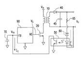
- FIG. 1shows a circuit schematic of a power converter.
- a control circuit 90generates a switching signal V G to regulate the output of the power converter in response to a feedback signal V FB at a feedback terminal FB.
- the switching signal V Gdrives a power transistor 20 for switching a transformer 10 .
- the transformer 10is connected to an input voltage V IN of the power converter for energy storage and power transfer. The energy of the transformer 10 is transferred to the output of the power converter through a rectifier 40 and a capacitor 45 .
- An output voltage V Ois coupled to an opto-coupler 50 through a resistor 65 and zener diode 60 .
- the output of the opto-coupler 50is connected to the feedback terminal FB of the controller 90 to form a feedback loop.
- the pulse width of the switching signal V Gis modulated in response to the feedback signal V FB to achieve the regulation of the power converter.
- FIG. 2shows a preferred embodiment of the controller 90 according to the present invention.
- the controller 90includes a comparison circuit 110 , an input circuit 100 , a switching circuit 200 , a soft start circuit 280 and an oscillation circuit 300 .
- the switching circuit 200is used to generate the switching signal V G in response to an oscillation signal PLS.
- the oscillation circuit 300is adapted to periodically generate the oscillation signal PLS and a ramp signal RAMP.
- the switching circuit 200includes a flip-flop 210 to generate the switching signal V G through an AND gate 230 .
- the input of the AND gate 230is connected to the output of the flip-flop 210 .
- Another input of the AND gate 230is connected to the oscillation signal PLS through an inverter 215 to limit the maximum duty cycle of the switching signal V G .
- the flip-flop 210is enabled in response to the oscillation signal PLS.
- An AND gate 253is coupled to reset the flip-flop 210 .
- the output of comparators 250 and 251are connected to inputs of the AND gate 253 .
- the positive input of the comparator 250is connected to the input circuit 100 .
- the negative input of the comparator 250is coupled to the ramp signal RAMP for the pulse width modulation (PWM).
- the negative input of the comparator 251is also coupled to the ramp signal RAMP.
- the positive input of the comparator 251is coupled to receive a soft start signal SS for the soft start of the switching signal V G .
- the input circuit 100includes a resistive device 150 and the feedback input circuit 240 .
- the feedback input circuit 240is coupled to the output of the power converter through the feedback terminal FB and the feedback loop of the power converter (shown in FIG. 1 ).
- a transistor 241 and resistors 245 and 246form the feedback input circuit 240 .
- the transistor 241performs the level shift.
- the feedback signal V FBis connected to the gate of the transistor 241 .
- a feedback signal V 245is generated at the source of the transistor 241 .
- Resistor 245 and 246further provides attenuation to the feedback signal V 245 to stabilize the feedback loop.
- the resistor 245is connected to the feedback signal V 245 .
- An attenuated feedback signal V 246is generated at the resistor 246 .
- the feedback signal V 246is connected to the positive input of the comparator 250 for PWM control.
- the comparison circuit 110is coupled to the feedback input circuit 240 to generate a mode signal LEN when the feedback signal V 245 is lower than a threshold signal V REF .
- the mode signal LENindicates the light load of the power converter. Wherein the mode signal LEN resets the soft start circuit for enabling soft start of the switching signal when switching signal is enabled.
- the control circuit 90further comprises an external capacitor 70 coupled to the input circuit 100 .
- An external capacitor 70is coupled to the feedback terminal FB as shown in FIG. 1 .
- a resistive device 150is coupled to the feedback terminal FB as well.
- the resistive device 150 and the external capacitor 70operate as a low-pass filter for the feedback signal V FB .
- a transistor 140 and resistors 120 and 125constitute the resistive device 150 .
- the resistor 120 and the resistor 125are connected in serial.
- the transistor 140is connected to the resistor 120 in parallel.
- the mode signal LENcontrols the on/off of the transistor 140 . Therefore, the resistance of the resistive device 150 is increased in response to the enablement of the mode signal LEN.
- the resistance of the input circuit 100will be increased once the mode signal LEN is enabled, which causes the feedback signal V FB to become low.
- the switching signal V Gwill be turned on again when the feedback signal V FB is charged up to a voltage V B .
- the voltage V Bcan be expressed as,
- V BV A ⁇ ( 1 - ⁇ - T OFF R ⁇ C ) ( 1 )
- V BV REF +V 241 (2)
- V AV A V CC ⁇ ( I C ⁇ R ) (3)
- I CCTR ⁇ I D (4)
- I DV O - V Z - V D R 65 ( 5 ) where T OFF is the off period of the switching signal V G ; R is the resistance of the resistive device 150 ; C is the capacitance of the external capacitor 70 ; V REF is the voltage of the threshold signal V REF ; V 241 is the threshold voltage of transistor 241 ; I C is a feedback current, which is the output current of the opto-coupler 50 (shown in FIG. 1 ); I D is the input current of the opto-coupler 50 (shown in FIG.
- CTRis the current transfer rate of the opto-coupler 50 ;
- V Dis the forward voltage drop of the opto-coupler 50 ;
- V Zis the voltage of the zener diode 60 ;
- R 65is the resistance of the resistor 65 .
- T OFFR ⁇ C ⁇ l n ( V A V A - V B ) ( 6 )
- the capacitance C of the external capacitor 70 associated with the resistance R of the resistive device 150determines the T OFF of the switching signal V G .
- the feedback current I Cis further coupled to adjust the T OFF to control the output ripple of the power converter.
- FIG. 3shows the oscillation circuit 300 according to a preferred embodiment of the present invention.
- a charge current 310is connected to a switch 315 in serial for charging a capacitor 350 .
- a discharge current 320is connected to a switch 325 in serial for discharging the capacitor 350 .
- the ramp signal RAMPis therefore generated on the capacitor 350 .
- Comparators 370 , 380 and NAND gates 375 , 385generate the oscillation signal PLS.
- the oscillation signal PLSis connected to control switches 315 and 325 through inverters 390 and 395 respectively.
- Trip-point voltages V H and V Lare connected to comparators 370 and 380 respectively.
- the ramp signal RAMPthus swings in between the trip-point voltage V H and V L .
- FIG. 4shows the soft start circuit 280 according to a preferred embodiment of the present invention.
- a charge current 291is connected to charge a capacitor 293 .
- a transistor 292is connected to the capacitor 293 in parallel for discharging the capacitor 293 .
- the soft start signal SSis generated on the capacitor 293 .
- An OR gate 295is connected to control the on/off of the transistor 292 .
- An input of the OR gate 295is connected to the mode signal LEN.
- Another input of the OR gate 295is coupled to a power-on-reset signal PWRST through an inverter 296 .
- a resistive device 297 and a capacitor 298generate the power-on-reset signal PWRST during the power on of the controller 90 . Therefore, the capacitor 293 is reset in response to the power-on-reset signal PWRST and/or the mode signal LEN.
- the soft start signal SSis further coupled to control the pulse width of the switching signal V G for the soft start.
- FIG. 5shows the switching signal VG and the mode signal LEN.
- the switching signal VGis enabled during the TON period.
- the period of TONis depended on the load condition and the feedback. Once the feedback signal V 245 is lower than the threshold signal VREF, the mode signal LEN will be enabled to turn off the switching signal VG.
- the TOFF periodcan be programmed by the external capacitor 70 to prevent the switching frequency of the switching signal VG from falling into the audio band.
Landscapes
- Engineering & Computer Science (AREA)
- Power Engineering (AREA)
- Dc-Dc Converters (AREA)
Abstract
Description
VB=VREF+V241 (2)
VAVCC−(IC×R) (3)
IC=CTR×ID (4)
where TOFFis the off period of the switching signal VG; R is the resistance of the
The equation (1) can be rewritten as,
The capacitance C of the
Claims (14)
Priority Applications (3)
| Application Number | Priority Date | Filing Date | Title |
|---|---|---|---|
| US11/626,026US7855899B2 (en) | 2007-01-23 | 2007-01-23 | Controller with loop impedance modulation for power converter |
| CN2007101658634ACN101159414B (en) | 2007-01-23 | 2007-11-07 | Control Circuits for Power Converters |
| TW096142189ATWI362812B (en) | 2007-01-23 | 2007-11-08 | Control circuit of power converter |
Applications Claiming Priority (1)
| Application Number | Priority Date | Filing Date | Title |
|---|---|---|---|
| US11/626,026US7855899B2 (en) | 2007-01-23 | 2007-01-23 | Controller with loop impedance modulation for power converter |
Publications (2)
| Publication Number | Publication Date |
|---|---|
| US20080174293A1 US20080174293A1 (en) | 2008-07-24 |
| US7855899B2true US7855899B2 (en) | 2010-12-21 |
Family
ID=39307374
Family Applications (1)
| Application Number | Title | Priority Date | Filing Date |
|---|---|---|---|
| US11/626,026Active2027-12-14US7855899B2 (en) | 2007-01-23 | 2007-01-23 | Controller with loop impedance modulation for power converter |
Country Status (3)
| Country | Link |
|---|---|
| US (1) | US7855899B2 (en) |
| CN (1) | CN101159414B (en) |
| TW (1) | TWI362812B (en) |
Cited By (4)
| Publication number | Priority date | Publication date | Assignee | Title |
|---|---|---|---|---|
| CN101320941A (en)* | 2007-06-07 | 2008-12-10 | 三星电子株式会社 | SMPS quasi-resonant converter, switch control circuit and its signal processing circuit |
| US20110051469A1 (en)* | 2005-04-21 | 2011-03-03 | Nicolas Cyr | Power supply control method and structure therefor |
| US10735412B2 (en)* | 2014-01-31 | 2020-08-04 | Apple Inc. | Use of a biometric image for authorization |
| US11676188B2 (en) | 2013-09-09 | 2023-06-13 | Apple Inc. | Methods of authenticating a user |
Families Citing this family (6)
| Publication number | Priority date | Publication date | Assignee | Title |
|---|---|---|---|---|
| US7936087B2 (en)* | 2007-03-12 | 2011-05-03 | System General Corp. | Switching controller for parallel power converters |
| TWI453564B (en)* | 2009-07-21 | 2014-09-21 | Richtek Technology Corp | Feedback circuit and control method of an isolated power converter |
| TWI475788B (en)* | 2012-06-07 | 2015-03-01 | Elite Semiconductor Esmt | Voltage converter with soft start circuitry |
| US9337737B2 (en)* | 2012-08-06 | 2016-05-10 | System General Corp. | Control circuit with fast dynamic response for power converters |
| TWI495236B (en)* | 2012-12-21 | 2015-08-01 | System General Corp | Control circuit and control method |
| US11539286B2 (en) | 2021-04-21 | 2022-12-27 | Quanta Computer Inc. | Clamping circuit |
Citations (11)
| Publication number | Priority date | Publication date | Assignee | Title |
|---|---|---|---|---|
| US4541041A (en) | 1983-08-22 | 1985-09-10 | General Electric Company | Full load to no-load control for a voltage fed resonant inverter |
| US4937728A (en)* | 1989-03-07 | 1990-06-26 | Rca Licensing Corporation | Switch-mode power supply with burst mode standby operation |
| US5028861A (en) | 1989-05-24 | 1991-07-02 | Motorola, Inc. | Strobed DC-DC converter with current regulation |
| US5481178A (en) | 1993-03-23 | 1996-01-02 | Linear Technology Corporation | Control circuit and method for maintaining high efficiency over broad current ranges in a switching regulator circuit |
| US5689407A (en)* | 1995-04-05 | 1997-11-18 | U.S. Philips Corporation | Switched-mode power supply |
| US5747977A (en) | 1995-03-30 | 1998-05-05 | Micro Linear Corporation | Switching regulator having low power mode responsive to load power consumption |
| US6370042B2 (en)* | 2000-03-17 | 2002-04-09 | Stmicroelectronics S.R.L. | Self-recovering disabling system for converter |
| US6487059B2 (en)* | 2000-07-31 | 2002-11-26 | Stmicroelectronics S.R.L. | Switching mode power supply device with detection of malfunctioning |
| US6906934B2 (en)* | 2003-09-04 | 2005-06-14 | System General Corp. | Integrated start-up circuit with reduced power consumption |
| US20050248965A1 (en)* | 2004-03-12 | 2005-11-10 | Tomoyasu Yamada | Switching dc power supply |
| US20050281062A1 (en)* | 2004-06-16 | 2005-12-22 | Jin-Ho Choi | Switching mode power supply |
Family Cites Families (4)
| Publication number | Priority date | Publication date | Assignee | Title |
|---|---|---|---|---|
| JP3391384B2 (en)* | 2000-12-04 | 2003-03-31 | サンケン電気株式会社 | DC-DC converter |
| US6597159B2 (en)* | 2001-08-15 | 2003-07-22 | System General Corp. | Pulse width modulation controller having frequency modulation for power converter |
| US6661679B1 (en)* | 2002-10-28 | 2003-12-09 | System General Corporation | PWM controller having adaptive off-time modulation for power saving |
| US6839247B1 (en)* | 2003-07-10 | 2005-01-04 | System General Corp. | PFC-PWM controller having a power saving means |
- 2007
- 2007-01-23USUS11/626,026patent/US7855899B2/enactiveActive
- 2007-11-07CNCN2007101658634Apatent/CN101159414B/ennot_activeExpired - Fee Related
- 2007-11-08TWTW096142189Apatent/TWI362812B/ennot_activeIP Right Cessation
Patent Citations (11)
| Publication number | Priority date | Publication date | Assignee | Title |
|---|---|---|---|---|
| US4541041A (en) | 1983-08-22 | 1985-09-10 | General Electric Company | Full load to no-load control for a voltage fed resonant inverter |
| US4937728A (en)* | 1989-03-07 | 1990-06-26 | Rca Licensing Corporation | Switch-mode power supply with burst mode standby operation |
| US5028861A (en) | 1989-05-24 | 1991-07-02 | Motorola, Inc. | Strobed DC-DC converter with current regulation |
| US5481178A (en) | 1993-03-23 | 1996-01-02 | Linear Technology Corporation | Control circuit and method for maintaining high efficiency over broad current ranges in a switching regulator circuit |
| US5747977A (en) | 1995-03-30 | 1998-05-05 | Micro Linear Corporation | Switching regulator having low power mode responsive to load power consumption |
| US5689407A (en)* | 1995-04-05 | 1997-11-18 | U.S. Philips Corporation | Switched-mode power supply |
| US6370042B2 (en)* | 2000-03-17 | 2002-04-09 | Stmicroelectronics S.R.L. | Self-recovering disabling system for converter |
| US6487059B2 (en)* | 2000-07-31 | 2002-11-26 | Stmicroelectronics S.R.L. | Switching mode power supply device with detection of malfunctioning |
| US6906934B2 (en)* | 2003-09-04 | 2005-06-14 | System General Corp. | Integrated start-up circuit with reduced power consumption |
| US20050248965A1 (en)* | 2004-03-12 | 2005-11-10 | Tomoyasu Yamada | Switching dc power supply |
| US20050281062A1 (en)* | 2004-06-16 | 2005-12-22 | Jin-Ho Choi | Switching mode power supply |
Cited By (6)
| Publication number | Priority date | Publication date | Assignee | Title |
|---|---|---|---|---|
| US20110051469A1 (en)* | 2005-04-21 | 2011-03-03 | Nicolas Cyr | Power supply control method and structure therefor |
| US8492924B2 (en)* | 2005-04-21 | 2013-07-23 | Seminconductor Components Industries, LLC | Power supply control method and structure therefor |
| CN101320941A (en)* | 2007-06-07 | 2008-12-10 | 三星电子株式会社 | SMPS quasi-resonant converter, switch control circuit and its signal processing circuit |
| US20080303491A1 (en)* | 2007-06-07 | 2008-12-11 | Samsung Electronics Co., Ltd | Switched-mode power supply quasi-resonant converter, switch control circuit controlling switching operations of switched-mode power supply quasi-resonant converter, and input signal processing circuit connected to control integrated circuit of switch control circuit |
| US11676188B2 (en) | 2013-09-09 | 2023-06-13 | Apple Inc. | Methods of authenticating a user |
| US10735412B2 (en)* | 2014-01-31 | 2020-08-04 | Apple Inc. | Use of a biometric image for authorization |
Also Published As
| Publication number | Publication date |
|---|---|
| CN101159414B (en) | 2010-06-09 |
| TW200832872A (en) | 2008-08-01 |
| US20080174293A1 (en) | 2008-07-24 |
| CN101159414A (en) | 2008-04-09 |
| TWI362812B (en) | 2012-04-21 |
Similar Documents
| Publication | Publication Date | Title |
|---|---|---|
| US7940035B2 (en) | Control circuit having an impedance modulation controlling power converter for saving power | |
| US7855899B2 (en) | Controller with loop impedance modulation for power converter | |
| US7778050B2 (en) | Energy transfer device and energy transfer control semiconductor device | |
| US9337737B2 (en) | Control circuit with fast dynamic response for power converters | |
| US8054656B2 (en) | Switching control circuit for a switching power converter | |
| US7426120B2 (en) | Switching control circuit having a valley voltage detector to achieve soft switching for a resonant power converter | |
| CN100421340C (en) | Flyback Power Converter | |
| US7957162B2 (en) | Switch mode power supply and driving method thereof | |
| US7378889B2 (en) | Pulse width modulation device with a power saving mode controlled by an output voltage feedback hysteresis circuit | |
| US9906149B2 (en) | Switching power supply with burst operation in standby mode | |
| US8553431B2 (en) | Switching power converter with load impedance detection | |
| US8488338B2 (en) | Controller with valley switching and limited maximum frequency for quasi-resonant power converters | |
| CN103904903B (en) | Flyback converter | |
| CN102969874B (en) | Control circuit with deep burst mode for power converter | |
| CN101997412B (en) | Control Method | |
| US11487311B2 (en) | Modulating jitter frequency as switching frequency approaches jitter frequency | |
| US20150280573A1 (en) | System and Method for a Switched-Mode Power Supply | |
| US20080309311A1 (en) | Power Converter for Compensating a maximum Output Power | |
| CN101572499A (en) | Switching controller with intermittent power-saving mode management circuit | |
| US20120069608A1 (en) | Control circuit with burst mode and extended valley switching for quasi-resonant power converter | |
| US6738266B2 (en) | Switching power supply unit | |
| CN102624238B (en) | Switching controller of flyback power converter and its controller and control circuit | |
| US9270184B2 (en) | Control circuit and terminal for cable compensation and wake-up of primary-side regulated power converter | |
| US7116565B1 (en) | Over-power protection apparatus for self-excited power converter | |
| US7466569B2 (en) | Power converter having phase lock circuit for quasi-resonant soft switching |
Legal Events
| Date | Code | Title | Description |
|---|---|---|---|
| AS | Assignment | Owner name:SYSTEM GENERAL CORP., TAIWAN Free format text:ASSIGNMENT OF ASSIGNORS INTEREST;ASSIGNOR:YANG, TA-YUNG;REEL/FRAME:018814/0183 Effective date:20070118 | |
| STCF | Information on status: patent grant | Free format text:PATENTED CASE | |
| FPAY | Fee payment | Year of fee payment:4 | |
| AS | Assignment | Owner name:FAIRCHILD (TAIWAN) CORPORATION, TAIWAN Free format text:CHANGE OF NAME;ASSIGNOR:SYSTEM GENERAL CORP.;REEL/FRAME:038594/0168 Effective date:20140620 | |
| AS | Assignment | Owner name:SEMICONDUCTOR COMPONENTS INDUSTRIES, LLC, ARIZONA Free format text:ASSIGNMENT OF ASSIGNORS INTEREST;ASSIGNOR:FAIRCHILD (TAIWAN) CORPORATION (FORMERLY SYSTEM GENERAL CORPORATION);REEL/FRAME:042328/0318 Effective date:20161221 | |
| MAFP | Maintenance fee payment | Free format text:PAYMENT OF MAINTENANCE FEE, 8TH YEAR, LARGE ENTITY (ORIGINAL EVENT CODE: M1552) Year of fee payment:8 | |
| AS | Assignment | Owner name:DEUTSCHE BANK AG NEW YORK BRANCH, AS COLLATERAL AGENT, NEW YORK Free format text:PATENT SECURITY AGREEMENT;ASSIGNOR:SEMICONDUCTOR COMPONENTS INDUSTRIES, LLC;REEL/FRAME:046410/0933 Effective date:20170210 Owner name:DEUTSCHE BANK AG NEW YORK BRANCH, AS COLLATERAL AG Free format text:PATENT SECURITY AGREEMENT;ASSIGNOR:SEMICONDUCTOR COMPONENTS INDUSTRIES, LLC;REEL/FRAME:046410/0933 Effective date:20170210 | |
| MAFP | Maintenance fee payment | Free format text:PAYMENT OF MAINTENANCE FEE, 12TH YEAR, LARGE ENTITY (ORIGINAL EVENT CODE: M1553); ENTITY STATUS OF PATENT OWNER: LARGE ENTITY Year of fee payment:12 | |
| AS | Assignment | Owner name:FAIRCHILD SEMICONDUCTOR CORPORATION, ARIZONA Free format text:RELEASE OF SECURITY INTEREST IN PATENTS RECORDED AT RECORDED AT REEL 046410, FRAME 0933;ASSIGNOR:DEUTSCHE BANK AG NEW YORK BRANCH, AS COLLATERAL AGENT;REEL/FRAME:064072/0001 Effective date:20230622 Owner name:SEMICONDUCTOR COMPONENTS INDUSTRIES, LLC, ARIZONA Free format text:RELEASE OF SECURITY INTEREST IN PATENTS RECORDED AT RECORDED AT REEL 046410, FRAME 0933;ASSIGNOR:DEUTSCHE BANK AG NEW YORK BRANCH, AS COLLATERAL AGENT;REEL/FRAME:064072/0001 Effective date:20230622 |