US7855401B2 - Passivation of wide band-gap based semiconductor devices with hydrogen-free sputtered nitrides - Google Patents
Passivation of wide band-gap based semiconductor devices with hydrogen-free sputtered nitridesDownload PDFInfo
- Publication number
- US7855401B2 US7855401B2US11/845,805US84580507AUS7855401B2US 7855401 B2US7855401 B2US 7855401B2US 84580507 AUS84580507 AUS 84580507AUS 7855401 B2US7855401 B2US 7855401B2
- Authority
- US
- United States
- Prior art keywords
- layer
- nitride
- passivation
- passivation structure
- silicon nitride
- Prior art date
- Legal status (The legal status is an assumption and is not a legal conclusion. Google has not performed a legal analysis and makes no representation as to the accuracy of the status listed.)
- Active, expires
Links
Images


Classifications
- H—ELECTRICITY
- H10—SEMICONDUCTOR DEVICES; ELECTRIC SOLID-STATE DEVICES NOT OTHERWISE PROVIDED FOR
- H10D—INORGANIC ELECTRIC SEMICONDUCTOR DEVICES
- H10D30/00—Field-effect transistors [FET]
- H10D30/01—Manufacture or treatment
- H10D30/015—Manufacture or treatment of FETs having heterojunction interface channels or heterojunction gate electrodes, e.g. HEMT
- H—ELECTRICITY
- H01—ELECTRIC ELEMENTS
- H01L—SEMICONDUCTOR DEVICES NOT COVERED BY CLASS H10
- H01L21/00—Processes or apparatus adapted for the manufacture or treatment of semiconductor or solid state devices or of parts thereof
- H01L21/02—Manufacture or treatment of semiconductor devices or of parts thereof
- H01L21/02104—Forming layers
- H01L21/02107—Forming insulating materials on a substrate
- H01L21/02109—Forming insulating materials on a substrate characterised by the type of layer, e.g. type of material, porous/non-porous, pre-cursors, mixtures or laminates
- H01L21/02112—Forming insulating materials on a substrate characterised by the type of layer, e.g. type of material, porous/non-porous, pre-cursors, mixtures or laminates characterised by the material of the layer
- H01L21/02123—Forming insulating materials on a substrate characterised by the type of layer, e.g. type of material, porous/non-porous, pre-cursors, mixtures or laminates characterised by the material of the layer the material containing silicon
- H01L21/0217—Forming insulating materials on a substrate characterised by the type of layer, e.g. type of material, porous/non-porous, pre-cursors, mixtures or laminates characterised by the material of the layer the material containing silicon the material being a silicon nitride not containing oxygen, e.g. SixNy or SixByNz
- H—ELECTRICITY
- H01—ELECTRIC ELEMENTS
- H01L—SEMICONDUCTOR DEVICES NOT COVERED BY CLASS H10
- H01L21/00—Processes or apparatus adapted for the manufacture or treatment of semiconductor or solid state devices or of parts thereof
- H01L21/02—Manufacture or treatment of semiconductor devices or of parts thereof
- H01L21/02104—Forming layers
- H01L21/02107—Forming insulating materials on a substrate
- H01L21/02225—Forming insulating materials on a substrate characterised by the process for the formation of the insulating layer
- H01L21/0226—Forming insulating materials on a substrate characterised by the process for the formation of the insulating layer formation by a deposition process
- H01L21/02263—Forming insulating materials on a substrate characterised by the process for the formation of the insulating layer formation by a deposition process deposition from the gas or vapour phase
- H—ELECTRICITY
- H01—ELECTRIC ELEMENTS
- H01L—SEMICONDUCTOR DEVICES NOT COVERED BY CLASS H10
- H01L21/00—Processes or apparatus adapted for the manufacture or treatment of semiconductor or solid state devices or of parts thereof
- H01L21/02—Manufacture or treatment of semiconductor devices or of parts thereof
- H01L21/04—Manufacture or treatment of semiconductor devices or of parts thereof the devices having potential barriers, e.g. a PN junction, depletion layer or carrier concentration layer
- H01L21/0445—Manufacture or treatment of semiconductor devices or of parts thereof the devices having potential barriers, e.g. a PN junction, depletion layer or carrier concentration layer the devices having semiconductor bodies comprising crystalline silicon carbide
- H01L21/045—Manufacture or treatment of semiconductor devices or of parts thereof the devices having potential barriers, e.g. a PN junction, depletion layer or carrier concentration layer the devices having semiconductor bodies comprising crystalline silicon carbide passivating silicon carbide surfaces
- H—ELECTRICITY
- H10—SEMICONDUCTOR DEVICES; ELECTRIC SOLID-STATE DEVICES NOT OTHERWISE PROVIDED FOR
- H10D—INORGANIC ELECTRIC SEMICONDUCTOR DEVICES
- H10D30/00—Field-effect transistors [FET]
- H10D30/40—FETs having zero-dimensional [0D], one-dimensional [1D] or two-dimensional [2D] charge carrier gas channels
- H10D30/47—FETs having zero-dimensional [0D], one-dimensional [1D] or two-dimensional [2D] charge carrier gas channels having 2D charge carrier gas channels, e.g. nanoribbon FETs or high electron mobility transistors [HEMT]
- H10D30/471—High electron mobility transistors [HEMT] or high hole mobility transistors [HHMT]
- H10D30/475—High electron mobility transistors [HEMT] or high hole mobility transistors [HHMT] having wider bandgap layer formed on top of lower bandgap active layer, e.g. undoped barrier HEMTs such as i-AlGaN/GaN HEMTs
- H10D30/4755—High electron mobility transistors [HEMT] or high hole mobility transistors [HHMT] having wider bandgap layer formed on top of lower bandgap active layer, e.g. undoped barrier HEMTs such as i-AlGaN/GaN HEMTs having wide bandgap charge-carrier supplying layers, e.g. modulation doped HEMTs such as n-AlGaAs/GaAs HEMTs
- H—ELECTRICITY
- H10—SEMICONDUCTOR DEVICES; ELECTRIC SOLID-STATE DEVICES NOT OTHERWISE PROVIDED FOR
- H10D—INORGANIC ELECTRIC SEMICONDUCTOR DEVICES
- H10D62/00—Semiconductor bodies, or regions thereof, of devices having potential barriers
- H10D62/80—Semiconductor bodies, or regions thereof, of devices having potential barriers characterised by the materials
- H10D62/83—Semiconductor bodies, or regions thereof, of devices having potential barriers characterised by the materials being Group IV materials, e.g. B-doped Si or undoped Ge
- H10D62/832—Semiconductor bodies, or regions thereof, of devices having potential barriers characterised by the materials being Group IV materials, e.g. B-doped Si or undoped Ge being Group IV materials comprising two or more elements, e.g. SiGe
- H10D62/8325—Silicon carbide
- H—ELECTRICITY
- H10—SEMICONDUCTOR DEVICES; ELECTRIC SOLID-STATE DEVICES NOT OTHERWISE PROVIDED FOR
- H10D—INORGANIC ELECTRIC SEMICONDUCTOR DEVICES
- H10D62/00—Semiconductor bodies, or regions thereof, of devices having potential barriers
- H10D62/80—Semiconductor bodies, or regions thereof, of devices having potential barriers characterised by the materials
- H10D62/85—Semiconductor bodies, or regions thereof, of devices having potential barriers characterised by the materials being Group III-V materials, e.g. GaAs
- H10D62/8503—Nitride Group III-V materials, e.g. AlN or GaN
Definitions
- the present inventionrelates to semiconductor structures and devices formed in wide bandgap materials such as the Group III nitrides.
- semiconductor devicesfundamentally depend upon the inherent properties of the semiconductor materials from which they are made, as well as the extent to which these materials can be incorporated in a useful device structure. Semiconductor devices also depend upon the manner in which various semiconductor materials are formed and arranged with respect to one another.
- One of the characteristics of semiconductor materialsis their bandgap; i.e., the energy difference between the valence band of electrons and the conductance band.
- the size of the material's bandgapprovides fundamental limitations upon—or possibilities for—device structures and performances.
- microwave systemstypically use solid state transistors as amplifiers and oscillators.
- solid state transistorsas amplifiers and oscillators.
- bandwidthbandwidth
- SiCsilicon carbide
- Ga, Al, InGroup III
- Higher bandgap materialsalso offer the potential for higher power capabilities (as compared to similar structures made from smaller bandgap materials) as well as the potential for emitting light at higher frequencies; e.g., the green, blue, violet and ultraviolet portions of the electromagnetic spectrum.
- Devices fabricated from silicon carbideare typically passivated with an oxide layer, such as SiO 2 , to protect the exposed SiC surfaces of the device, or for other reasons, or both.
- oxide layersuch as SiO 2
- the interface between SiC and SiO 2may be insufficient to obtain a high surface mobility of electrons. More specifically, the interface between SiC and SiO 2 conventionally exhibits a high density of interface states, which may reduce surface electron mobility and introduce carrier traps, which in turn reduces the desired performance characteristics of devices such as (but not limited to) metal-oxide-semiconductor field-effect transistors (MOSFETs).
- MOSFETsmetal-oxide-semiconductor field-effect transistors
- semiconductor devicesincluding those that include oxidation layers, also incorporate one or more layers of silicon nitride to improve the resulting electronic properties (e.g., U.S. Pat. No. 6,246,076).
- Silicon nitridealso provides an environmental barrier that the oxide fails to provide, or without which, would allow the environment to degrade the structure and operation of the device, regardless of whether the device includes an oxide layer.
- silicon nitrideis preferred over silicon dioxide because it forms a better seal over the device, preventing contaminants such as water from reaching the epitaxial layers of the device and from causing degradation.
- Silicon nitridemay also be used to form layers that transmit light generated within an LED.
- nitridedoes not provide the open channels found in oxide structures; thus, nitride is widely employed in electronics as a barrier material.
- hydrogendiffuses slowly in a densified nitride film, and other small positive ions (Na + or K + ) are effectively blocked by thin nitride layers. Because oxygen diffuses very slowly through nitride, deposited nitride can prevent oxidation of underlying silicon.
- nitrides deposited using chemical vapor depositionalmost always contain hydrogen, typically much more than in the comparable oxide films.
- the source of the hydrogenis the silane (SiH 4 ) precursor and also the ammonia (NH 3 ) employed in many CVD schemes.
- An amorphous, but constrained, film such as silicon nitridecan discourage the atoms from occupying positions that fill the valences of each silicon and nitrogen atom. Thus, many broken bonds tend to be present. These bonds are readily occupied by hydrogen atoms.
- conventional plasma nitridescan have as much as 20 atomic percent hydrogen, bonded both to the Si and N atoms, and; thermal nitrides still have several percent hydrogen even after high-temperature anneals.
- hydrogencan passivate Mg-acceptors in a GaN-based semiconductor.
- silicon nitrideis deposited by means of PECVD at a deposition temperature in excess of 200° C.
- hydrogen in the filmcan diffuse through thin ohmic contacts or other layers and into nearby Group III nitride layers, causing them to become passivated in a region close to their surface. That is, in a region near the surface, a substantial number of acceptor ions are rendered neutral by the introduction of hydrogen in the film. Accordingly, an interface between an ohmic contact and a nitride material is degraded, and the contact metal does not exhibit ideal ohmic characteristics. This can result in an increase in forward voltage (V f degradation) in the device. Essentially, the device will behave as though the interface between a metal and a Group III nitride contact layer forms a Schottky contact instead of an ohmic contact.
- nitride passivation layersare often used in conjunction with oxide layers, the hydrogen can migrate to the oxide layers.
- hydrogen in oxide films on SiChas been shown to alter the interface Fermi level and encourage a state of surface accumulation. Any resulting accumulation layer produces a charge layer that alters the device capacitance and exhibits a drift with a long time constant caused by the mobility of the hydrogen in the film.
- oxide and nitride layersoffer certain advantages, they also raise certain problems that can limit or degrade device performance.
- the inventionis an improved field effect transistor formed in the Group III nitride material system.
- the improvementincludes a two part passivation structure in which a chemical vapor deposited passivation layer of silicon nitride encapsulates a previously sputtered-deposited layer of silicon nitride.
- the sputtered layerprovides some of the benefits of passivation and the chemical vapor deposited layer provides an excellent environmental barrier.
- the inventionis a high electron mobility transistor (HEMT).
- HEMThigh electron mobility transistor
- the inventionincludes a Group III heterostructure, a first passivation structure on the Group III nitride layer for reducing parasitic capacitance and minimizing device trapping, and a second passivation structure on the first passivation structure for encapsulating the structure and providing an environmental barrier.
- the first passivation structureincludes at least one sputtered layer of non-stoichiometric nitride selected from the group consisting of silicon nitride, aluminum nitride, oxynitrides of silicon and oxynitrides of aluminum, and at least one chemical vapor deposited layer of silicon nitride for positioning the passivation layers further from said Group III nitride layer without fully encapsulating said structure.
- the second passivation structureincludes an environmental barrier of stoichiometric nitrides.
- the inventionis an insulated gate field effect transistor that includes a Group III nitride heterostructure, respective source and drain ohmic contacts on the heterostructure, an insulating layer on the heterostructure between the source and drain ohmic contacts, a gate contact to the insulating layer on the heterostructure, and respective first and second passivation structures on the heterostructure and at least portions of the gate contact.
- the first passivation structureincludes at least one sputtered layer of non-stoichiometric nitride selected from the group consisting of silicon nitride, aluminum nitride, oxynitrides of silicon and oxynitrides of aluminum, and at least one chemical vapor deposited layer of silicon nitride for positioning the passivation layers further from the Group III nitride heterostructure without fully encapsulating the transistor.
- the second passivation structureincludes an environmental barrier of stoichiometric nitrides.
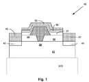
- FIG. 1is a schematic cross sectional view of a Group III nitride based device that incorporates the present invention.
- FIG. 2is a schematic view of a sputtering system used in conjunction with the present invention.
- FIG. 3is across sectional schematic view of another Group III nitride based high electron mobility transistor that incorporates the invention.
- FIG. 4is another embodiment of the Group III nitride high electron mobility transistor that incorporates the invention.
- FIG. 5is yet another embodiment of a Group III nitride high electron mobility transistor that incorporates the passivation system of the invention.
- FIG. 6is an embodiment of a Group III nitride high electron mobility transistor with a field plate that incorporates the passivation system of the invention.
- the inventionis a passivated semiconductor structure and resulting passivated semiconductor devices.
- the inventioncan be broadly considered as a two part structure in which a chemical vapor deposited passivation layer of silicon nitride encapsulates a previously sputtered-deposited layer of silicon nitride.
- the sputtered layerprovides some of the benefits of passivation and the chemical vapor deposited layer provides an excellent environmental barrier.
- the inventionis a two-part structure formed of a stoichiometric layer of silicon nitride deposited upon a non-stoichiometric layer of silicon nitride.
- the non-stoichiometric layerenhances the electronic properties of the structure or resulting device and the stoichiometric layer provides an excellent environmental barrier.
- FIGS. 1 and 3 - 6illustrate the invention in the context of respective exemplary devices. It will be understood that the invention is not limited to the illustrated devices or to particular families of devices, but can be incorporated as desired or needed in a wide variety of devices familiar to those of skill in this art.
- the materials for the ohmic and gate contactscan be selected from a plurality of metals or highly conductive semiconductors and that this can be accomplished without undue experimentation by those of skill in this art.
- FIG. 1illustrates a metal-semiconductor field-effect transistor (MESFET) 40 based on gallium nitride (GaN) or aluminum gallium nitride (AlGaN) as the semiconductor.
- the device 40includes a gallium nitride or aluminum gallium nitride layer 41 and potentially can include an additional substrate (or substrate and buffer structure) which is designated by the dotted rectangle 42 .
- a bulk crystal of gallium nitridecan theoretically eliminate the need for the substrate and buffer 42 , but most devices of this type will include a substrate of SiC or sapphire or some other suitable material.
- the aluminum gallium nitrideis best expressed as Al x Ga 1-x N where 0 ⁇ x ⁇ 1.
- the atomic fractions of aluminum and galliumcan be selected as desired or necessary based upon the intended structure and operation of the device
- the device 40includes the source region 43 and the drain region 44 with ohmic contacts 46 and 47 made to the source 43 and drain 44 respectively to define a channel 39 therebetween.
- a first passivation structure formed of nonstoichiometric silicon nitrideis on the Group III nitride layer 41 .
- the first passivation structurereduces parasitic capacitance and minimizes device trapping and positions subsequent passivation layers further from the channel 39 .
- the first passivation structurecomprises two layers 50 and 51 of sputtered non-stoichiometric silicon nitride on the Group III nitride layer 41 .
- Layer 50can also include low-hydrogen, high quality, stoichiometric silicon nitride or silicon dioxide.
- the second passivation structurecomprises a sputtered-deposited layer 52 of silicon nitride on the first passivation structure, and in particular on the layer 51 , and a chemical vapor deposited layer 53 of silicon nitride on the sputter-deposited layer 52 .
- both of the layers 52 and 53comprise stoichiometric silicon nitride.
- the sputtered layers 50 and 51are advantageously substantially hydrogen free, and similarly because the layer 52 is also sputtered, it is likewise substantially hydrogen free and have a refractive index of between about 1.85 and 2.05.
- the first sputtered nonstoichiometric layer 50reduces parasitic capacitance and minimizing device trapping.
- the second sputtered non-stoichiometric silicon nitride layer 51positions subsequent passivation layers further from the substrate 42 , but without fully encapsulating the transistor 40 .
- the sputtered stoichiometric silicon nitride layer 52initially encapsulates the transistor 40 and enhances the hydrogen barrier properties of the passivation layers.
- the chemical vapor deposited environmental barrier layer 53covers the transistor 40 to provide step coverage and crack prevention.
- the first two sputtered layers 50 and 51are preferentially nitrogen-rich.
- the proportion of silicon or nitrogen (in a non-stoichiometric composition)can be determined by the refractive index, which is an indicator of the composition of the formed silicon nitride film.
- a silicon nitride film having a substantially stoichiometric compositionhas a refractive index of 2.02 measured @ 6328 ⁇ .
- Silicon rich nitridehas an atomic ratio of silicon to nitrogen that is greater than 3:4 (i.e., stoichiometric silicon nitride is Si 3 N4).
- a typical silicon rich nitridewill have an index of refraction of greater than 2.02 measured @6328 ⁇ and a nitrogen rich SiN film will have an index of refraction lower than 2.02 measured @6328 ⁇ .
- each of the nonstoichiometric sputtered silicon nitride layershave a refractive index of between about 1.85 and 1.95.
- sputteringis to avoid the presence of hydrogen as described elsewhere herein, and to correspondingly avoid the electronic problems associated with the presence of hydrogen. Accordingly, the sputtered layers can also be understood as hydrogen-free layers. Stated differently, sputtering is one technique for producing a hydrogen-free passivation layer. The invention, however, can also be understood as the hydrogen free passivation layer regardless of its method of manufacture.
- FIG. 2is a schematic diagram of a sputtering system 60 similar to the one set forth in U.S. Pat. No. 6,586,781.
- the substrate upon which the sputter layer is intendedis indicated at 61 on an electrode (anode) 62 in a chamber 63 .
- the pressure in the chamber 63is typically reduced using a vacuum pump 59 and the desired gas or gases (typically inert or noble gases such as argon) are added to the chamber 63 through the passage 64 and controlled by the valve 65 .
- gas moleculesbecome ionized and accelerate to impinge upon (in this case) the silicon target 66 which also serves as the cathode.
- the impinging gas ionwill eject silicon ions or atoms 72 which then deposit on the substrate 61 as indicated by the small circles 68 .
- FIG. 3is another embodiment of Group III nitride-based HEMT according to the invention.
- the transistoris broadly designated at 75 and where the same elements are illustrated as in FIG. 1 , they will carry the same reference numerals.
- FIG. 6illustrates that a HEMT according to the invention can be formed on respective (barrier) layer 76 and (channel) layer 77 of Group III nitride.
- the adjacent layers 76 and 77have different compositions and thus produce the hetero structure for the transistor.
- these layersare typically positioned on a substrate such as 42 ( FIG. 1 ) which, as noted earlier, is frequently silicon carbide.
- FIG. 3also illustrates two additional Group III nitride spacer layers 80 and 81 that, when present, can enhance the response of the transistor.
- the low field mobility of the transistorcan be limited by the presence of doping impurities and lattice vibrations which can adversely affect the movement of the electrons in the device channel. Physically separating the impurities from the channel with thin layers such as 80 and 81 can address this issue and enhance the transistor's performance.
- the layer 76is formed of aluminum gallium nitride and the layers 77 is formed of gallium nitride to produce the heterostructure for the transistor 75 .
- the layer 80is formed of gallium nitride and the layer 81 is formed of aluminum nitride.
- the transistor 75can include the first sputtered silicon nitride or aluminum nitride layer 50 and the second sputtered silicon nitride layer 51 , both of which may be non-stoichiometric, hydrogen free, and have the desired refractive index of between about 1.85 and 2.05.
- the encapsulating stoichiometric silicon nitride layeris again illustrated at 52 and the stoichiometric plasma enhanced chemically vapor deposited layer is again illustrated at 53 .
- the layer 50can be formed from one of several different passivation materials. These can include high-quality stoichiometric silicon nitride (Si 3 N 4 ) deposited in a manner that yields low hydrogen content, low oxygen content and very low to zero buffered oxide etch (BOE), high quality stoichiometric silicon nitride with a covering layer of silicon dioxide, a stack of sputtered silicon nitride and plasma enhanced chemical vapor deposited silicon nitride; metal organic chemical vapor deposited (MOCVD) silicon nitride, or plasma enhanced chemical vapor deposition (PECVD) silicon nitride, most preferably using a high density plasma chemical vapor deposition system where molecular nitrogen (N 2 ) can be used as the nitrogen source instead of ammonia (NH 3 ) to advantageously minimize or eliminate the presence of hydrogen in the.
- Si 3 N 4high-quality stoichiometric silicon nitride
- BOEbuffered oxide etch
- the passivation layer 51is typically the sputtered silicon nitride while the passivation layer 52 can include the high quality stoichiometric silicon nitride, the plasma enhanced chemically vapor deposited silicon nitride, or plasma enhanced chemical vapor deposited oxynitride.
- the final layer 53can include the high-quality stoichiometric silicon nitride, the plasma enhanced chemical vapor deposited silicon nitride, or the plasma enhanced chemical vapor deposited oxynitride.
- the transistor illustrated in FIG. 3can include a field plate (not shown) in a manner analogous to the structure illustrated in FIG. 6 herein.
- FIG. 4illustrates an insulated gate transistor that incorporates the present invention.
- the respective passivation structure illustrated by the layers 50 , 51 , 52 and 53is the same as described with respect to the earlier figures.
- FIG. 4illustrates a transistor broadly designated at 82 that also includes an insulating layer 83 between the gate contact 32 and the heterostructure formed by the layers 76 and 77 (and potentially the layers 80 and 81 ).
- FIG. 5illustrates another insulated gate transistor that incorporates the passivation structure of the invention broadly designated at 84 .
- the insulating layer 85has portions that are again positioned between the gate contact 32 and the heterostructure formed by the Group III nitride layers 76 , 77 , 80 , and 81 .
- the insulating layer 85also, however, has portions that extend above and over the first sputtered silicon nitride layer 50 but covered entirely by the second sputtered silicon nitride layer 51 .
- FIG. 6illustrates a high electron mobility transistor according to the invention that further includes a field plate 91 .
- elements that are, or can be, the same as in the other embodimentscarry the same reference numerals.
- FIG. 6broadly illustrates the transistor at 87 and illustrates that it includes all of the elements of FIG. 3
- the field plate 91is positioned to overlap the gate contact 90 .
- This overlapping structureeliminates the need to fabricate a device with a carefully monitored lateral separation between the gate and the field plate.
- the overlapping relationship between the field plate 91 and the gate 90can introduce unwanted additional capacitance.
- the field plate 91does not overlap the gate 90 , but in such circumstances, the lateral relationship between the gate contact 90 and the field plate 91 must be carefully controlled in order to make sure that the field plate 91 is isolated from the gate 90 while still maximizing the field effect provided by the field plate 91 .
- the field plate 91is spaced from the gate 90 by layers 51 and 52 , but in turn is covered by layer 53 .
- the use of the field plate 91can reduce the electric field in the device, in turn resulting in an increased breakdown voltage and reduced trapping. Reducing the electric field with the field plate can also reduce leakage current and enhance the transistor's reliability.
- the field plate 91is typically connected to the source electrode 46 which reduces gain and instability, and the shielding effect can enhance input-output isolation.
- the inventionis a method of passivating Group III nitride based structures and devices.
- the inventionis a method comprising sputter-depositing a non-stoichiometric silicon nitride layer, and depositing an environmental barrier of stoichiometric silicon nitride (Si 3 N 4 ) by chemical vapor deposition, and in exemplary cases, by plasma enhanced chemical vapor deposition.
- Exemplary annealing techniquesare set forth in U.S. Pat. No.
- the sputteringis carried out using a silicon target in a substantially hydrogen-free environment, which can incorporate argon (Ar) and nitrogen (N 2 ).
- the methodcan include sputtering with a pulsed direct current (DC) power source to thereby discharge insulating particles while avoiding arcing.
- DCdirect current
- the sputteringcan be carried out at room temperature, or at an elevated substrate temperature. If the sputtering is carried out at an elevated substrate temperature, it should be carried out in a manner that avoids exceeding temperatures that would otherwise detrimentally affect the remainder of the device.
- the substrate temperaturecan be raised to between about 350° C. and 450° C. without detrimental effects.
- the substrate temperature and the gas pressureare typically interrelated and thus are controlled accordingly.
- the methodcan comprise sputtering in a nitrogen-rich environment to provide a nonstoichiometric silicon nitride.
- the environmental barrieris typically formed of a stoichiometric silicon nitride layer because of its better barrier properties as compared to the nonstoichiometric silicon nitride layer.
- the ion bombardmentcan be enhanced by applying a radio frequency biased to the substrate, or by lowering the ambient pressure during the sputtering step.
- the methodcan be carried out in substantially the same manner for Group III nitride based devices, with the exception that a thermal oxide is not included and the silicon nitride is sputtered directly on the Group III nitride device or structure.
- the first passivationis deposited after T gates are formed.
- the first passivation for GaN devicesconsists of two layers. A sputtered SiN or AlN is deposited on top surface of the GaN (typically AlGaN). This is followed by a PECVD SiN film.
- the salient featureis again, to move a typical hydrogen contaminated PECVD nitride film away from the device interface and replace it with a sputtered nitride film (SiN or AlN).
- This filmcan also be an oxynitride of Si or Al.
- a PECVD SiN filmis deposited on top of the sputtered passivation layer. The PECVD film offers good step coverage under the gates, when necessary.
- the second passivation of the GaN devicescan use sputtered nitrides or PECVD nitrides or the combination of both.
- the second passivationis added after gates and T top are formed.
- the second passivationconsists of three dielectric layers.
- the first two dielectric layersare sputtered SiN.
- the first sputtered SiN layer of 100 to 3000 ⁇is a nitrogen rich film (N 2 flow of 14 to 18 sccm and process pressure of 7 to 10 mT) with refractive index in the range of 1.85 to 2.00. This film moves the subsequent passivation layers away from the device interface, but does not yet encapsulate.
- the second sputtered SiN layer with thickness of 1000 to 3000 ⁇is a stoichiometric nitride with refractive index of 2.04 measured at 630 nm.
- This filmis deposited at lower nitrogen flow and higher bombardment (N 2 flow of 12 to 14 sccm and process pressure of 1 to 3 mT).
- N 2 flow12 to 14 sccm and process pressure of 1 to 3 mT.
- the encapsulating properties of this filmare improved by ion bombardment, either through lower pressure, or using RF bias on the wafers (about 0.5 W/inch 2 ).
- the sputtered SiN filmprovides good encapsulation, and also moves the third dielectric layer further away from the device interface.
- the second sputtered SiN layermay not offer adequate step coverage. This is addressed in the third dielectric layer.
- a 2000 to 5000 ⁇ PECVD SiN layeris deposited on top of the sputtered SiN layers using SiH 4 2%, 350 sccm; NH 3 , 4 sccm; N 2 , 200 sccm; He, 90 sccm; pressure, 1 Torr; power, 25 W.
- the critical process parameter in the PECVD SiN depositionis substrate temperature; higher substrate temperatures tend to drive hydrogen out of the film. The substrate temperature is kept as high as other existing films on the wafer allow, typically between about 250° C. to 450° C.
- the stoichiometric sputtered SiN filmoffers a barrier to the hydrogen present during PECVD deposition.
- the PECVDoffers a final environmental encapsulant with excellent step coverage.
Landscapes
- Engineering & Computer Science (AREA)
- Microelectronics & Electronic Packaging (AREA)
- Condensed Matter Physics & Semiconductors (AREA)
- General Physics & Mathematics (AREA)
- Manufacturing & Machinery (AREA)
- Computer Hardware Design (AREA)
- Physics & Mathematics (AREA)
- Power Engineering (AREA)
- Chemical & Material Sciences (AREA)
- Crystallography & Structural Chemistry (AREA)
- Junction Field-Effect Transistors (AREA)
- Formation Of Insulating Films (AREA)
- Insulated Gate Type Field-Effect Transistor (AREA)
Abstract
Description
Claims (31)
Priority Applications (4)
| Application Number | Priority Date | Filing Date | Title |
|---|---|---|---|
| US11/845,805US7855401B2 (en) | 2005-06-29 | 2007-08-28 | Passivation of wide band-gap based semiconductor devices with hydrogen-free sputtered nitrides |
| JP2008218759AJP2009055042A (en) | 2007-08-28 | 2008-08-27 | Passivation of wide band gap based semiconductor devices with sputtered nitrides without hydrogen |
| EP08163116.0AEP2031648B1 (en) | 2007-08-28 | 2008-08-27 | Passivation of wide band-gap based semiconductor devices with hydrogen-free sputtered nitrides |
| JP2013077659AJP2013168663A (en) | 2007-08-28 | 2013-04-03 | Passivation of wide band-gap based semiconductor device with hydrogen-free sputtered nitride |
Applications Claiming Priority (2)
| Application Number | Priority Date | Filing Date | Title |
|---|---|---|---|
| US11/169,378US7525122B2 (en) | 2005-06-29 | 2005-06-29 | Passivation of wide band-gap based semiconductor devices with hydrogen-free sputtered nitrides |
| US11/845,805US7855401B2 (en) | 2005-06-29 | 2007-08-28 | Passivation of wide band-gap based semiconductor devices with hydrogen-free sputtered nitrides |
Related Parent Applications (1)
| Application Number | Title | Priority Date | Filing Date |
|---|---|---|---|
| US11/169,378Continuation-In-PartUS7525122B2 (en) | 2005-06-29 | 2005-06-29 | Passivation of wide band-gap based semiconductor devices with hydrogen-free sputtered nitrides |
Publications (2)
| Publication Number | Publication Date |
|---|---|
| US20080035934A1 US20080035934A1 (en) | 2008-02-14 |
| US7855401B2true US7855401B2 (en) | 2010-12-21 |
Family
ID=40070550
Family Applications (1)
| Application Number | Title | Priority Date | Filing Date |
|---|---|---|---|
| US11/845,805Active2027-03-27US7855401B2 (en) | 2005-06-29 | 2007-08-28 | Passivation of wide band-gap based semiconductor devices with hydrogen-free sputtered nitrides |
Country Status (3)
| Country | Link |
|---|---|
| US (1) | US7855401B2 (en) |
| EP (1) | EP2031648B1 (en) |
| JP (2) | JP2009055042A (en) |
Cited By (43)
| Publication number | Priority date | Publication date | Assignee | Title |
|---|---|---|---|---|
| US20100073067A1 (en)* | 2008-09-23 | 2010-03-25 | Transphorm Inc. | Inductive Load Power Switching Circuits |
| US20110127541A1 (en)* | 2008-12-10 | 2011-06-02 | Transphorm Inc. | Semiconductor heterostructure diodes |
| US20110127604A1 (en)* | 2009-11-30 | 2011-06-02 | Ken Sato | Semiconductor device |
| US20120119261A1 (en)* | 2009-07-28 | 2012-05-17 | Panasonic Corporation | Semiconductor device |
| US8389977B2 (en) | 2009-12-10 | 2013-03-05 | Transphorm Inc. | Reverse side engineered III-nitride devices |
| US8390000B2 (en) | 2009-08-28 | 2013-03-05 | Transphorm Inc. | Semiconductor devices with field plates |
| US20130161692A1 (en)* | 2011-12-21 | 2013-06-27 | Alexei Koudymov | Shield wrap for a heterostructure field effect transistor |
| US8519438B2 (en) | 2008-04-23 | 2013-08-27 | Transphorm Inc. | Enhancement mode III-N HEMTs |
| US8598937B2 (en) | 2011-10-07 | 2013-12-03 | Transphorm Inc. | High power semiconductor electronic components with increased reliability |
| US8643062B2 (en) | 2011-02-02 | 2014-02-04 | Transphorm Inc. | III-N device structures and methods |
| US8716141B2 (en) | 2011-03-04 | 2014-05-06 | Transphorm Inc. | Electrode configurations for semiconductor devices |
| US8742459B2 (en) | 2009-05-14 | 2014-06-03 | Transphorm Inc. | High voltage III-nitride semiconductor devices |
| US8742460B2 (en) | 2010-12-15 | 2014-06-03 | Transphorm Inc. | Transistors with isolation regions |
| US8772842B2 (en) | 2011-03-04 | 2014-07-08 | Transphorm, Inc. | Semiconductor diodes with low reverse bias currents |
| US8901604B2 (en) | 2011-09-06 | 2014-12-02 | Transphorm Inc. | Semiconductor devices with guard rings |
| US8912839B2 (en) | 2008-02-12 | 2014-12-16 | Transphorm Inc. | Bridge circuits and their components |
| US8994073B2 (en) | 2012-10-04 | 2015-03-31 | Cree, Inc. | Hydrogen mitigation schemes in the passivation of advanced devices |
| US20150108547A1 (en)* | 2013-10-17 | 2015-04-23 | Samsung Electronics Co., Ltd. | High electron mobility transistor |
| US9059076B2 (en) | 2013-04-01 | 2015-06-16 | Transphorm Inc. | Gate drivers for circuits based on semiconductor devices |
| US9093366B2 (en) | 2012-04-09 | 2015-07-28 | Transphorm Inc. | N-polar III-nitride transistors |
| US9165766B2 (en) | 2012-02-03 | 2015-10-20 | Transphorm Inc. | Buffer layer structures suited for III-nitride devices with foreign substrates |
| US9171730B2 (en) | 2013-02-15 | 2015-10-27 | Transphorm Inc. | Electrodes for semiconductor devices and methods of forming the same |
| US9184275B2 (en) | 2012-06-27 | 2015-11-10 | Transphorm Inc. | Semiconductor devices with integrated hole collectors |
| US9190295B2 (en) | 2009-11-02 | 2015-11-17 | Transphorm Inc. | Package configurations for low EMI circuits |
| US9224721B2 (en) | 2012-02-24 | 2015-12-29 | Transphorm Inc. | Semiconductor power modules and devices |
| US9245992B2 (en) | 2013-03-15 | 2016-01-26 | Transphorm Inc. | Carbon doping semiconductor devices |
| US9257547B2 (en) | 2011-09-13 | 2016-02-09 | Transphorm Inc. | III-N device structures having a non-insulating substrate |
| US9318593B2 (en) | 2014-07-21 | 2016-04-19 | Transphorm Inc. | Forming enhancement mode III-nitride devices |
| US9401708B2 (en) | 2014-05-20 | 2016-07-26 | General Electric Company | Gate drive unit and method for controlling a gate drive unit |
| US9443938B2 (en) | 2013-07-19 | 2016-09-13 | Transphorm Inc. | III-nitride transistor including a p-type depleting layer |
| US9443941B2 (en)* | 2012-06-04 | 2016-09-13 | Infineon Technologies Austria Ag | Compound semiconductor transistor with self aligned gate |
| US9536967B2 (en) | 2014-12-16 | 2017-01-03 | Transphorm Inc. | Recessed ohmic contacts in a III-N device |
| US9537425B2 (en) | 2013-07-09 | 2017-01-03 | Transphorm Inc. | Multilevel inverters and their components |
| US9536966B2 (en) | 2014-12-16 | 2017-01-03 | Transphorm Inc. | Gate structures for III-N devices |
| US9543940B2 (en) | 2014-07-03 | 2017-01-10 | Transphorm Inc. | Switching circuits having ferrite beads |
| US9590060B2 (en) | 2013-03-13 | 2017-03-07 | Transphorm Inc. | Enhancement-mode III-nitride devices |
| US9590494B1 (en) | 2014-07-17 | 2017-03-07 | Transphorm Inc. | Bridgeless power factor correction circuits |
| US9812338B2 (en) | 2013-03-14 | 2017-11-07 | Cree, Inc. | Encapsulation of advanced devices using novel PECVD and ALD schemes |
| US9991399B2 (en) | 2012-10-04 | 2018-06-05 | Cree, Inc. | Passivation structure for semiconductor devices |
| US10200030B2 (en) | 2015-03-13 | 2019-02-05 | Transphorm Inc. | Paralleling of switching devices for high power circuits |
| US10224401B2 (en) | 2016-05-31 | 2019-03-05 | Transphorm Inc. | III-nitride devices including a graded depleting layer |
| US10319648B2 (en) | 2017-04-17 | 2019-06-11 | Transphorm Inc. | Conditions for burn-in of high power semiconductors |
| US11322599B2 (en) | 2016-01-15 | 2022-05-03 | Transphorm Technology, Inc. | Enhancement mode III-nitride devices having an Al1-xSixO gate insulator |
Families Citing this family (26)
| Publication number | Priority date | Publication date | Assignee | Title |
|---|---|---|---|---|
| US7855401B2 (en) | 2005-06-29 | 2010-12-21 | Cree, Inc. | Passivation of wide band-gap based semiconductor devices with hydrogen-free sputtered nitrides |
| US7525122B2 (en)* | 2005-06-29 | 2009-04-28 | Cree, Inc. | Passivation of wide band-gap based semiconductor devices with hydrogen-free sputtered nitrides |
| US7800132B2 (en)* | 2007-10-25 | 2010-09-21 | Northrop Grumman Systems Corporation | High electron mobility transistor semiconductor device having field mitigating plate and fabrication method thereof |
| WO2010111228A2 (en)* | 2009-03-25 | 2010-09-30 | Dow Global Technologies Inc. | Method of forming a protective layer on thin-film photovoltaic articles and articles made with such a layer |
| WO2012024114A2 (en)* | 2010-08-20 | 2012-02-23 | Applied Materials, Inc. | Methods for forming a hydrogen free silicon containing dielectric film |
| WO2014109830A1 (en)* | 2013-01-08 | 2014-07-17 | Applied Materials, Inc. | Metal oxynitride based heterojunction field effect transistor |
| JP2014138111A (en)* | 2013-01-17 | 2014-07-28 | Fujitsu Ltd | Semiconductor device and manufacturing method of the same, power supply device and high-frequency amplifier |
| JP6339762B2 (en)* | 2013-01-17 | 2018-06-06 | 富士通株式会社 | Semiconductor device and manufacturing method thereof, power supply device, and high-frequency amplifier |
| US9425267B2 (en)* | 2013-03-14 | 2016-08-23 | Freescale Semiconductor, Inc. | Transistor with charge enhanced field plate structure and method |
| JP2015050335A (en)* | 2013-09-02 | 2015-03-16 | ルネサスエレクトロニクス株式会社 | Semiconductor device |
| JP6301640B2 (en)* | 2013-11-28 | 2018-03-28 | ルネサスエレクトロニクス株式会社 | Semiconductor device and manufacturing method of semiconductor device |
| JP2015213100A (en)* | 2014-05-01 | 2015-11-26 | 三菱電機株式会社 | Semiconductor device and method for manufacturing the same |
| US9754787B2 (en)* | 2014-06-24 | 2017-09-05 | Infineon Technologies Ag | Method for treating a semiconductor wafer |
| WO2016059889A1 (en)* | 2014-10-14 | 2016-04-21 | シャープ株式会社 | Nitride semiconductor device |
| CN107431021B (en)* | 2015-03-31 | 2020-09-22 | 夏普株式会社 | Nitride semiconductor field effect transistor |
| US9580304B2 (en)* | 2015-05-07 | 2017-02-28 | Texas Instruments Incorporated | Low-stress low-hydrogen LPCVD silicon nitride |
| WO2017069464A1 (en)* | 2015-10-22 | 2017-04-27 | (주)기가레인 | High-electron-mobility transistor and method for fabricating same |
| JP6300773B2 (en) | 2015-10-23 | 2018-03-28 | 三菱電機株式会社 | Semiconductor pressure sensor |
| JP6640687B2 (en)* | 2016-09-09 | 2020-02-05 | 株式会社東芝 | Semiconductor device |
| DE102018110240A1 (en)* | 2018-04-27 | 2019-10-31 | Infineon Technologies Ag | Semiconductor device and manufacturing |
| US11760696B2 (en)* | 2019-01-04 | 2023-09-19 | Rtx Corporation | Ceramic matrix composite component with modified thermal expansion and method for producing the same |
| US10971612B2 (en) | 2019-06-13 | 2021-04-06 | Cree, Inc. | High electron mobility transistors and power amplifiers including said transistors having improved performance and reliability |
| US10923585B2 (en) | 2019-06-13 | 2021-02-16 | Cree, Inc. | High electron mobility transistors having improved contact spacing and/or improved contact vias |
| US20220384366A1 (en)* | 2021-06-01 | 2022-12-01 | Cree, Inc. | Multilayer encapsulation for humidity robustness and related fabrication methods |
| US20230207640A1 (en)* | 2021-12-29 | 2023-06-29 | Nxp Usa, Inc. | Transistor gate structure with insulating layer and method of fabrication therefor |
| US20230317634A1 (en)* | 2022-04-05 | 2023-10-05 | Applied Materials, Inc. | Coatings with diffusion barriers for corrosion and contamination protection |
Citations (65)
| Publication number | Priority date | Publication date | Assignee | Title |
|---|---|---|---|---|
| US3895127A (en) | 1974-04-19 | 1975-07-15 | Rca Corp | Method of selectively depositing glass on semiconductor devices |
| US3982267A (en) | 1974-04-16 | 1976-09-21 | Thomson-Csf | Pin diode with a thick intrinsic zone and a device comprising such a diode |
| US4551353A (en) | 1981-12-30 | 1985-11-05 | Unitrode Corporation | Method for reducing leakage currents in semiconductor devices |
| US4717641A (en) | 1986-01-16 | 1988-01-05 | Motorola Inc. | Method for passivating a semiconductor junction |
| US4799100A (en) | 1987-02-17 | 1989-01-17 | Siliconix Incorporated | Method and apparatus for increasing breakdown of a planar junction |
| US5332697A (en) | 1989-05-31 | 1994-07-26 | Smith Rosemary L | Formation of silicon nitride by nitridation of porous silicon |
| US5430324A (en) | 1992-07-23 | 1995-07-04 | Siliconix, Incorporated | High voltage transistor having edge termination utilizing trench technology |
| US5466617A (en) | 1992-03-20 | 1995-11-14 | U.S. Philips Corporation | Manufacturing electronic devices comprising TFTs and MIMs |
| US5650638A (en) | 1995-01-03 | 1997-07-22 | Abb Research Ltd. | Semiconductor device having a passivation layer |
| US5776837A (en) | 1992-06-05 | 1998-07-07 | Cree Research, Inc. | Method of obtaining high quality silicon dioxide passivation on silicon carbide and resulting passivated structures |
| US5972801A (en) | 1995-11-08 | 1999-10-26 | Cree Research, Inc. | Process for reducing defects in oxide layers on silicon carbide |
| US6001716A (en) | 1998-05-22 | 1999-12-14 | United Silicon Incorporated | Fabricating method of a metal gate |
| WO2001013436A1 (en) | 1999-08-16 | 2001-02-22 | Cornell Research Foundation, Inc. | Passivation of gan based fets |
| US6246076B1 (en) | 1998-08-28 | 2001-06-12 | Cree, Inc. | Layered dielectric on silicon carbide semiconductor structures |
| US20010023964A1 (en) | 2000-02-04 | 2001-09-27 | Yifeng Wu | Group III nitride based FETs and hemts with reduced trapping and method for producing the same |
| US20010028100A1 (en) | 1997-07-25 | 2001-10-11 | Hughes Electronics Corporation. | Passivation layer and process for semiconductor devices |
| EP1149934A2 (en) | 2000-04-28 | 2001-10-31 | Asm Japan K.K. | CVD synthesis of silicon nitride materials |
| US20010050369A1 (en) | 1999-06-28 | 2001-12-13 | Intersil Corporation | Edge termination for silicon power devices |
| US20020052076A1 (en) | 2000-09-27 | 2002-05-02 | Khan Muhammad Asif | Metal oxide semiconductor heterostructure field effect transistor |
| US6396090B1 (en) | 2000-09-22 | 2002-05-28 | Industrial Technology Research Institute | Trench MOS device and termination structure |
| WO2002049114A2 (en) | 2000-12-12 | 2002-06-20 | The Kansai Electric Power Co., Inc. | High withstand voltage semiconductor device |
| US6426542B1 (en) | 1998-05-01 | 2002-07-30 | Allen Tan | Schottky diode with dielectric trench |
| US6429518B1 (en) | 1998-10-05 | 2002-08-06 | Tokyo Electron Ltd. | Semiconductor device having a fluorine-added carbon film as an inter-layer insulating film |
| US20020121641A1 (en) | 1999-12-07 | 2002-09-05 | Philips Electronics North America Corporation | Passivated silicon carbide devices with low leakage current and method of fabricating |
| US20030020092A1 (en)* | 2001-07-24 | 2003-01-30 | Primit Parikh | Insulating gate AlGaN/GaN HEMT |
| US20030025121A1 (en) | 1997-08-29 | 2003-02-06 | Edmond John Adam | Robust Group III light emitting diode for high reliability in standard packaging applications |
| US6528373B2 (en) | 2001-02-12 | 2003-03-04 | Cree, Inc. | Layered dielectric on silicon carbide semiconductor structures |
| US6610366B2 (en) | 2000-10-03 | 2003-08-26 | Cree, Inc. | Method of N2O annealing an oxide layer on a silicon carbide layer |
| US20030160274A1 (en) | 1998-08-28 | 2003-08-28 | Das Mrinal Kanti | Methods of fabricating high voltage, high temperature capacitor and interconnection structures |
| US6673662B2 (en) | 2000-11-28 | 2004-01-06 | Cree, Inc. | Epitaxial edge termination for silicon carbide Schottky devices and methods of fabricating silicon carbide devices incorporating same |
| TW579600B (en) | 2001-05-11 | 2004-03-11 | Cree Inc | Group-III nitride based high electron mobility transistor (HEMT) with barrier/spacer layer |
| US20040099928A1 (en) | 2002-11-27 | 2004-05-27 | Nunan Thomas K. | Composite dielectric with improved etch selectivity for high voltage mems structures |
| US20040099888A1 (en) | 2002-11-26 | 2004-05-27 | Saptharishi Sriram | Transistors having buried p-type layers beneath the source region |
| US20040118202A1 (en) | 2002-12-13 | 2004-06-24 | Denso Corporation | Flow sensor having thin film portion and method for manufacturing the same |
| US6767843B2 (en) | 2000-10-03 | 2004-07-27 | Cree, Inc. | Method of N2O growth of an oxide layer on a silicon carbide layer |
| US20040159865A1 (en) | 2000-05-10 | 2004-08-19 | Allen Scott T. | Methods of fabricating silicon carbide metal-semiconductor field effect transistors |
| US20040160118A1 (en) | 2002-11-08 | 2004-08-19 | Knollenberg Clifford F. | Actuator apparatus and method for improved deflection characteristics |
| US6797586B2 (en) | 2001-06-28 | 2004-09-28 | Koninklijke Philips Electronics N.V. | Silicon carbide schottky barrier diode and method of making |
| US20050019971A1 (en) | 2001-07-23 | 2005-01-27 | Slater David B. | Methods of fabricating light emitting devices using mesa regions and passivation layers |
| US20050097941A1 (en) | 2003-11-12 | 2005-05-12 | General Electric Company | Gas sensor device |
| US20050156284A1 (en) | 2003-12-16 | 2005-07-21 | Infineon Technologies Ag | Semiconductor component having a pn junction and a passivation layer applied on a surface |
| US20050170574A1 (en) | 2004-01-16 | 2005-08-04 | Sheppard Scott T. | Nitride-based transistors with a protective layer and a low-damage recess and methods of fabrication thereof |
| US6939756B1 (en) | 2000-03-24 | 2005-09-06 | Vanderbilt University | Inclusion of nitrogen at the silicon dioxide-silicon carbide interace for passivation of interface defects |
| US20050193800A1 (en) | 2001-03-29 | 2005-09-08 | Deboer John | Porous gas sensors and method of preparation thereof |
| US20050212075A1 (en) | 2004-03-16 | 2005-09-29 | Ixys Semiconductor Gmbh | Power semiconductor component in the planar technique |
| US20050221628A1 (en) | 2004-03-30 | 2005-10-06 | Eudyna Devices Inc. | Semiconductor device and method of fabricating the same |
| US20050258431A1 (en) | 2004-05-22 | 2005-11-24 | Smith Richard P | Dielectric passivation for semiconductor devices |
| WO2005114743A2 (en) | 2004-05-11 | 2005-12-01 | Cree, Inc. | Wide bandgap transistors with multiple field plates |
| US20050274980A1 (en)* | 2004-06-15 | 2005-12-15 | Ngk Insulators, Ltd. | Semiconductor multilayer structure, semiconductor device and HEMT device |
| US20050285233A1 (en) | 2004-06-24 | 2005-12-29 | Taiwan Semiconductor Manufacturing Co., Ltd. | Thin film transistor (TFT) device structure employing silicon rich silicon oxide passivation layer |
| US20060006414A1 (en)* | 2004-06-30 | 2006-01-12 | Marianne Germain | AlGaN/GaN high electron mobility transistor devices |
| US20060006415A1 (en) | 2004-05-11 | 2006-01-12 | Cree, Inc. | Wide bandgap HEMTs with source connected field plates |
| US20060043437A1 (en) | 2004-08-24 | 2006-03-02 | Chandra Mouli | Transparent metal shielded isolation for image sensors |
| US20060043379A1 (en) | 2004-08-31 | 2006-03-02 | An-Ping Zhang | SIC metal semiconductor field-effect transistors and methods for producing same |
| US20060118892A1 (en) | 2004-12-02 | 2006-06-08 | Taiwan Semiconductor Manufacturing Company, Ltd. | Methods and Structures to Produce a Strain-Inducing Layer in a Semiconductor Device |
| US20060145190A1 (en) | 2004-12-31 | 2006-07-06 | Salzman David B | Surface passivation for III-V compound semiconductors |
| US20060157733A1 (en) | 2003-06-13 | 2006-07-20 | Gerald Lucovsky | Complex oxides for use in semiconductor devices and related methods |
| US20060191474A1 (en)* | 2005-02-02 | 2006-08-31 | Agency For Science, Technology And Research | Method and structure for fabricating III-V nitride layers on silicon substrates |
| US20070001176A1 (en) | 2005-06-29 | 2007-01-04 | Ward Allan Iii | Environmentally robust passivation structures for high-voltage silicon carbide semiconductor devices |
| US20070001174A1 (en) | 2005-06-29 | 2007-01-04 | Zoltan Ring | Passivation of wide band-gap based semiconductor devices with hydrogen-free sputtered nitrides |
| WO2007064689A1 (en) | 2005-12-02 | 2007-06-07 | Nitronex Corporation | Gallium nitride material devices and associated methods |
| EP1798762A2 (en) | 2005-12-13 | 2007-06-20 | Cree Inc. | Semiconductor devices including implanted regions and protective layers and methods of forming the same |
| US20070164322A1 (en) | 2006-01-17 | 2007-07-19 | Cree, Inc. | Methods of fabricating transistors including dielectrically-supported gate electrodes and related devices |
| US20070164321A1 (en) | 2006-01-17 | 2007-07-19 | Cree, Inc. | Methods of fabricating transistors including supported gate electrodes and related devices |
| US20080035934A1 (en) | 2005-06-29 | 2008-02-14 | Sheppard Scott T | Passivation of Wide Band-Gap Based Semiconductor Devices with Hydrogen-Free Sputtered Nitrides |
Family Cites Families (3)
| Publication number | Priority date | Publication date | Assignee | Title |
|---|---|---|---|---|
| US11791385B2 (en)* | 2005-03-11 | 2023-10-17 | Wolfspeed, Inc. | Wide bandgap transistors with gate-source field plates |
| US20070018198A1 (en)* | 2005-07-20 | 2007-01-25 | Brandes George R | High electron mobility electronic device structures comprising native substrates and methods for making the same |
| US20070018199A1 (en)* | 2005-07-20 | 2007-01-25 | Cree, Inc. | Nitride-based transistors and fabrication methods with an etch stop layer |
- 2007
- 2007-08-28USUS11/845,805patent/US7855401B2/enactiveActive
- 2008
- 2008-08-27EPEP08163116.0Apatent/EP2031648B1/enactiveActive
- 2008-08-27JPJP2008218759Apatent/JP2009055042A/enactivePending
- 2013
- 2013-04-03JPJP2013077659Apatent/JP2013168663A/enactivePending
Patent Citations (78)
| Publication number | Priority date | Publication date | Assignee | Title |
|---|---|---|---|---|
| US3982267A (en) | 1974-04-16 | 1976-09-21 | Thomson-Csf | Pin diode with a thick intrinsic zone and a device comprising such a diode |
| US3895127A (en) | 1974-04-19 | 1975-07-15 | Rca Corp | Method of selectively depositing glass on semiconductor devices |
| US4551353A (en) | 1981-12-30 | 1985-11-05 | Unitrode Corporation | Method for reducing leakage currents in semiconductor devices |
| US4717641A (en) | 1986-01-16 | 1988-01-05 | Motorola Inc. | Method for passivating a semiconductor junction |
| US4799100A (en) | 1987-02-17 | 1989-01-17 | Siliconix Incorporated | Method and apparatus for increasing breakdown of a planar junction |
| US5332697A (en) | 1989-05-31 | 1994-07-26 | Smith Rosemary L | Formation of silicon nitride by nitridation of porous silicon |
| US5466617A (en) | 1992-03-20 | 1995-11-14 | U.S. Philips Corporation | Manufacturing electronic devices comprising TFTs and MIMs |
| US5776837A (en) | 1992-06-05 | 1998-07-07 | Cree Research, Inc. | Method of obtaining high quality silicon dioxide passivation on silicon carbide and resulting passivated structures |
| US5605852A (en) | 1992-07-23 | 1997-02-25 | Siliconix Incorporated | Method for fabricating high voltage transistor having trenched termination |
| US5430324A (en) | 1992-07-23 | 1995-07-04 | Siliconix, Incorporated | High voltage transistor having edge termination utilizing trench technology |
| US5650638A (en) | 1995-01-03 | 1997-07-22 | Abb Research Ltd. | Semiconductor device having a passivation layer |
| US5972801A (en) | 1995-11-08 | 1999-10-26 | Cree Research, Inc. | Process for reducing defects in oxide layers on silicon carbide |
| US20010028100A1 (en) | 1997-07-25 | 2001-10-11 | Hughes Electronics Corporation. | Passivation layer and process for semiconductor devices |
| US20030025121A1 (en) | 1997-08-29 | 2003-02-06 | Edmond John Adam | Robust Group III light emitting diode for high reliability in standard packaging applications |
| US6825501B2 (en) | 1997-08-29 | 2004-11-30 | Cree, Inc. | Robust Group III light emitting diode for high reliability in standard packaging applications |
| US20030201453A2 (en) | 1997-08-29 | 2003-10-30 | Cree, Inc. | Robust Group III Light Emitting Diode for High Reliability in Standard Packaging Applications |
| US6426542B1 (en) | 1998-05-01 | 2002-07-30 | Allen Tan | Schottky diode with dielectric trench |
| TW471049B (en) | 1998-05-22 | 2002-01-01 | United Microelectronics Corp | Metal gate structure and manufacturing method for metal oxide semiconductor |
| US6001716A (en) | 1998-05-22 | 1999-12-14 | United Silicon Incorporated | Fabricating method of a metal gate |
| US6246076B1 (en) | 1998-08-28 | 2001-06-12 | Cree, Inc. | Layered dielectric on silicon carbide semiconductor structures |
| US20030160274A1 (en) | 1998-08-28 | 2003-08-28 | Das Mrinal Kanti | Methods of fabricating high voltage, high temperature capacitor and interconnection structures |
| US20010009788A1 (en) | 1998-08-28 | 2001-07-26 | Lipkin Lori A. | Layered dielectric on silicon carbide semiconductor structures |
| US6437371B2 (en) | 1998-08-28 | 2002-08-20 | Cree, Inc. | Layered dielectric on silicon carbide semiconductor structures |
| US6429518B1 (en) | 1998-10-05 | 2002-08-06 | Tokyo Electron Ltd. | Semiconductor device having a fluorine-added carbon film as an inter-layer insulating film |
| US20010050369A1 (en) | 1999-06-28 | 2001-12-13 | Intersil Corporation | Edge termination for silicon power devices |
| TW474024B (en) | 1999-08-16 | 2002-01-21 | Cornell Res Foundation Inc | Passivation of GaN based FETs |
| WO2001013436A1 (en) | 1999-08-16 | 2001-02-22 | Cornell Research Foundation, Inc. | Passivation of gan based fets |
| US20020121641A1 (en) | 1999-12-07 | 2002-09-05 | Philips Electronics North America Corporation | Passivated silicon carbide devices with low leakage current and method of fabricating |
| US20010023964A1 (en) | 2000-02-04 | 2001-09-27 | Yifeng Wu | Group III nitride based FETs and hemts with reduced trapping and method for producing the same |
| US6586781B2 (en) | 2000-02-04 | 2003-07-01 | Cree Lighting Company | Group III nitride based FETs and HEMTs with reduced trapping and method for producing the same |
| US6939756B1 (en) | 2000-03-24 | 2005-09-06 | Vanderbilt University | Inclusion of nitrogen at the silicon dioxide-silicon carbide interace for passivation of interface defects |
| EP1149934A2 (en) | 2000-04-28 | 2001-10-31 | Asm Japan K.K. | CVD synthesis of silicon nitride materials |
| US20040159865A1 (en) | 2000-05-10 | 2004-08-19 | Allen Scott T. | Methods of fabricating silicon carbide metal-semiconductor field effect transistors |
| US6396090B1 (en) | 2000-09-22 | 2002-05-28 | Industrial Technology Research Institute | Trench MOS device and termination structure |
| US20020052076A1 (en) | 2000-09-27 | 2002-05-02 | Khan Muhammad Asif | Metal oxide semiconductor heterostructure field effect transistor |
| US6610366B2 (en) | 2000-10-03 | 2003-08-26 | Cree, Inc. | Method of N2O annealing an oxide layer on a silicon carbide layer |
| US6767843B2 (en) | 2000-10-03 | 2004-07-27 | Cree, Inc. | Method of N2O growth of an oxide layer on a silicon carbide layer |
| US6673662B2 (en) | 2000-11-28 | 2004-01-06 | Cree, Inc. | Epitaxial edge termination for silicon carbide Schottky devices and methods of fabricating silicon carbide devices incorporating same |
| WO2002049114A2 (en) | 2000-12-12 | 2002-06-20 | The Kansai Electric Power Co., Inc. | High withstand voltage semiconductor device |
| US6528373B2 (en) | 2001-02-12 | 2003-03-04 | Cree, Inc. | Layered dielectric on silicon carbide semiconductor structures |
| US20050193800A1 (en) | 2001-03-29 | 2005-09-08 | Deboer John | Porous gas sensors and method of preparation thereof |
| TW579600B (en) | 2001-05-11 | 2004-03-11 | Cree Inc | Group-III nitride based high electron mobility transistor (HEMT) with barrier/spacer layer |
| US6849882B2 (en) | 2001-05-11 | 2005-02-01 | Cree Inc. | Group-III nitride based high electron mobility transistor (HEMT) with barrier/spacer layer |
| US6797586B2 (en) | 2001-06-28 | 2004-09-28 | Koninklijke Philips Electronics N.V. | Silicon carbide schottky barrier diode and method of making |
| US20050019971A1 (en) | 2001-07-23 | 2005-01-27 | Slater David B. | Methods of fabricating light emitting devices using mesa regions and passivation layers |
| US20030020092A1 (en)* | 2001-07-24 | 2003-01-30 | Primit Parikh | Insulating gate AlGaN/GaN HEMT |
| US20040160118A1 (en) | 2002-11-08 | 2004-08-19 | Knollenberg Clifford F. | Actuator apparatus and method for improved deflection characteristics |
| US20040099888A1 (en) | 2002-11-26 | 2004-05-27 | Saptharishi Sriram | Transistors having buried p-type layers beneath the source region |
| US20040099928A1 (en) | 2002-11-27 | 2004-05-27 | Nunan Thomas K. | Composite dielectric with improved etch selectivity for high voltage mems structures |
| US20040118202A1 (en) | 2002-12-13 | 2004-06-24 | Denso Corporation | Flow sensor having thin film portion and method for manufacturing the same |
| US20060157733A1 (en) | 2003-06-13 | 2006-07-20 | Gerald Lucovsky | Complex oxides for use in semiconductor devices and related methods |
| US20050097941A1 (en) | 2003-11-12 | 2005-05-12 | General Electric Company | Gas sensor device |
| US20050156284A1 (en) | 2003-12-16 | 2005-07-21 | Infineon Technologies Ag | Semiconductor component having a pn junction and a passivation layer applied on a surface |
| US20050170574A1 (en) | 2004-01-16 | 2005-08-04 | Sheppard Scott T. | Nitride-based transistors with a protective layer and a low-damage recess and methods of fabrication thereof |
| WO2005076365A1 (en) | 2004-01-16 | 2005-08-18 | Cree, Inc. | Nitride-based transistors with a protective layer and a low-damage recess and methods of fabrication thereof |
| US20050212075A1 (en) | 2004-03-16 | 2005-09-29 | Ixys Semiconductor Gmbh | Power semiconductor component in the planar technique |
| US20050221628A1 (en) | 2004-03-30 | 2005-10-06 | Eudyna Devices Inc. | Semiconductor device and method of fabricating the same |
| WO2005114743A2 (en) | 2004-05-11 | 2005-12-01 | Cree, Inc. | Wide bandgap transistors with multiple field plates |
| US20060006415A1 (en) | 2004-05-11 | 2006-01-12 | Cree, Inc. | Wide bandgap HEMTs with source connected field plates |
| US20050258431A1 (en) | 2004-05-22 | 2005-11-24 | Smith Richard P | Dielectric passivation for semiconductor devices |
| US20050274980A1 (en)* | 2004-06-15 | 2005-12-15 | Ngk Insulators, Ltd. | Semiconductor multilayer structure, semiconductor device and HEMT device |
| US20050285233A1 (en) | 2004-06-24 | 2005-12-29 | Taiwan Semiconductor Manufacturing Co., Ltd. | Thin film transistor (TFT) device structure employing silicon rich silicon oxide passivation layer |
| US20060006414A1 (en)* | 2004-06-30 | 2006-01-12 | Marianne Germain | AlGaN/GaN high electron mobility transistor devices |
| US20060043437A1 (en) | 2004-08-24 | 2006-03-02 | Chandra Mouli | Transparent metal shielded isolation for image sensors |
| US20060043379A1 (en) | 2004-08-31 | 2006-03-02 | An-Ping Zhang | SIC metal semiconductor field-effect transistors and methods for producing same |
| US20060118892A1 (en) | 2004-12-02 | 2006-06-08 | Taiwan Semiconductor Manufacturing Company, Ltd. | Methods and Structures to Produce a Strain-Inducing Layer in a Semiconductor Device |
| US20060145190A1 (en) | 2004-12-31 | 2006-07-06 | Salzman David B | Surface passivation for III-V compound semiconductors |
| US20060191474A1 (en)* | 2005-02-02 | 2006-08-31 | Agency For Science, Technology And Research | Method and structure for fabricating III-V nitride layers on silicon substrates |
| US20070018272A1 (en) | 2005-06-29 | 2007-01-25 | Henning Jason P | Reduced Leakage Power Devices By Inversion Layer Surface Passivation |
| US20070001174A1 (en) | 2005-06-29 | 2007-01-04 | Zoltan Ring | Passivation of wide band-gap based semiconductor devices with hydrogen-free sputtered nitrides |
| US20070001176A1 (en) | 2005-06-29 | 2007-01-04 | Ward Allan Iii | Environmentally robust passivation structures for high-voltage silicon carbide semiconductor devices |
| US20080035934A1 (en) | 2005-06-29 | 2008-02-14 | Sheppard Scott T | Passivation of Wide Band-Gap Based Semiconductor Devices with Hydrogen-Free Sputtered Nitrides |
| US20090215280A1 (en) | 2005-06-29 | 2009-08-27 | Cree, Inc. | Passivation of Wide Band-Gap Based Semiconductor Devices with Hydrogen-Free Sputtered Nitrides |
| US7598576B2 (en) | 2005-06-29 | 2009-10-06 | Cree, Inc. | Environmentally robust passivation structures for high-voltage silicon carbide semiconductor devices |
| WO2007064689A1 (en) | 2005-12-02 | 2007-06-07 | Nitronex Corporation | Gallium nitride material devices and associated methods |
| EP1798762A2 (en) | 2005-12-13 | 2007-06-20 | Cree Inc. | Semiconductor devices including implanted regions and protective layers and methods of forming the same |
| US20070164322A1 (en) | 2006-01-17 | 2007-07-19 | Cree, Inc. | Methods of fabricating transistors including dielectrically-supported gate electrodes and related devices |
| US20070164321A1 (en) | 2006-01-17 | 2007-07-19 | Cree, Inc. | Methods of fabricating transistors including supported gate electrodes and related devices |
Non-Patent Citations (9)
| Title |
|---|
| Chung et al, Effect of Nitric Oxide Annealing on the Interface Trap Densities Near the Band Edges in the 4H Polytype of Silicon Carbide; Applied Physics Letters, vol. 76, No. 13, Mar. 2000, pp. 1713-1715. |
| European Search Report for EP 08 16 3116 dated Jan. 15, 2010, 2 pages. |
| Ganem et al, "NRA and XPS Characterizations of Layers Formed by Rapid Thermal Nitridation of Thin SI02 Films," Nuclear Instruments & Methods in Physics Research, Section-B: Beam Interactions With Materials and Atoms, Elsevier, Amsterdam, NL, vol. 1364, No. 1-4, 1992, pp. 744-749. |
| International Search Report and Written Opinion for International Application No. PCT/US2006/048817, mailed Jun. 25, 2007. |
| Li et al, Improving SiO2 Grown on P-Type 4H-SiC by NO Annealing, Materials Science Forum; vols. 264-268, 1998, pp. 869-872 Trans Tech Publications, Switzerland. |
| Lipkin et al, "Improved Oxidation Procedures for Reduced SiO2/SiC Defects," Journal of Electronic Materials; vol. 25, No. 5, 1996, pp. 909-915. |
| Lipkin et al, N2O Processing Improves the 4H-SiC:SiO2 Interface; Materials Science Forum, vols. 389-393, 2002, pp. 985-988, 2002 Trans Tech Publications, Switzerland. |
| Ohno et al, "Effect of surface passivation on breakdown of AIGaN/an HEMTs," Compound Semiconductors, 2003, International Symposium, Aug. 25-27, 2003, Piscataway, NJ, pp. 169-170. |
| ROC (Taiwan) Search Report of foreign counterpart application No. 095123557; date of completion Jan. 15, 2009; 1 pg. |
Cited By (97)
| Publication number | Priority date | Publication date | Assignee | Title |
|---|---|---|---|---|
| US8912839B2 (en) | 2008-02-12 | 2014-12-16 | Transphorm Inc. | Bridge circuits and their components |
| US9899998B2 (en) | 2008-02-12 | 2018-02-20 | Transphorm Inc. | Bridge circuits and their components |
| US9437708B2 (en) | 2008-04-23 | 2016-09-06 | Transphorm Inc. | Enhancement mode III-N HEMTs |
| US8841702B2 (en) | 2008-04-23 | 2014-09-23 | Transphorm Inc. | Enhancement mode III-N HEMTs |
| US9941399B2 (en) | 2008-04-23 | 2018-04-10 | Transphorm Inc. | Enhancement mode III-N HEMTs |
| US8519438B2 (en) | 2008-04-23 | 2013-08-27 | Transphorm Inc. | Enhancement mode III-N HEMTs |
| US9196716B2 (en) | 2008-04-23 | 2015-11-24 | Transphorm Inc. | Enhancement mode III-N HEMTs |
| US8289065B2 (en) | 2008-09-23 | 2012-10-16 | Transphorm Inc. | Inductive load power switching circuits |
| US9690314B2 (en) | 2008-09-23 | 2017-06-27 | Transphorm Inc. | Inductive load power switching circuits |
| US20100073067A1 (en)* | 2008-09-23 | 2010-03-25 | Transphorm Inc. | Inductive Load Power Switching Circuits |
| US8493129B2 (en) | 2008-09-23 | 2013-07-23 | Transphorm Inc. | Inductive load power switching circuits |
| US8816751B2 (en) | 2008-09-23 | 2014-08-26 | Transphorm Inc. | Inductive load power switching circuits |
| US8531232B2 (en) | 2008-09-23 | 2013-09-10 | Transphorm Inc. | Inductive load power switching circuits |
| US8541818B2 (en)* | 2008-12-10 | 2013-09-24 | Transphorm Inc. | Semiconductor heterostructure diodes |
| US20120267640A1 (en)* | 2008-12-10 | 2012-10-25 | Transphorm Inc. | Semiconductor heterostructure diodes |
| US8237198B2 (en)* | 2008-12-10 | 2012-08-07 | Transphorm Inc. | Semiconductor heterostructure diodes |
| US20140054603A1 (en)* | 2008-12-10 | 2014-02-27 | Transphorm Inc. | Semiconductor Heterostructure Diodes |
| US9041065B2 (en)* | 2008-12-10 | 2015-05-26 | Transphorm Inc. | Semiconductor heterostructure diodes |
| US20110127541A1 (en)* | 2008-12-10 | 2011-06-02 | Transphorm Inc. | Semiconductor heterostructure diodes |
| US8742459B2 (en) | 2009-05-14 | 2014-06-03 | Transphorm Inc. | High voltage III-nitride semiconductor devices |
| US9293561B2 (en) | 2009-05-14 | 2016-03-22 | Transphorm Inc. | High voltage III-nitride semiconductor devices |
| US8692292B2 (en)* | 2009-07-28 | 2014-04-08 | Panasonic Corporation | Semiconductor device including separated gate electrode and conductive layer |
| US20120119261A1 (en)* | 2009-07-28 | 2012-05-17 | Panasonic Corporation | Semiconductor device |
| US9831315B2 (en) | 2009-08-28 | 2017-11-28 | Transphorm Inc. | Semiconductor devices with field plates |
| US8692294B2 (en) | 2009-08-28 | 2014-04-08 | Transphorm Inc. | Semiconductor devices with field plates |
| US8390000B2 (en) | 2009-08-28 | 2013-03-05 | Transphorm Inc. | Semiconductor devices with field plates |
| US9373699B2 (en) | 2009-08-28 | 2016-06-21 | Transphorm Inc. | Semiconductor devices with field plates |
| US9111961B2 (en) | 2009-08-28 | 2015-08-18 | Transphorm Inc. | Semiconductor devices with field plates |
| US9190295B2 (en) | 2009-11-02 | 2015-11-17 | Transphorm Inc. | Package configurations for low EMI circuits |
| US20110127604A1 (en)* | 2009-11-30 | 2011-06-02 | Ken Sato | Semiconductor device |
| US10199217B2 (en) | 2009-12-10 | 2019-02-05 | Transphorm Inc. | Methods of forming reverse side engineered III-nitride devices |
| US8389977B2 (en) | 2009-12-10 | 2013-03-05 | Transphorm Inc. | Reverse side engineered III-nitride devices |
| US9496137B2 (en) | 2009-12-10 | 2016-11-15 | Transphorm Inc. | Methods of forming reverse side engineered III-nitride devices |
| US9437707B2 (en) | 2010-12-15 | 2016-09-06 | Transphorm Inc. | Transistors with isolation regions |
| US8742460B2 (en) | 2010-12-15 | 2014-06-03 | Transphorm Inc. | Transistors with isolation regions |
| US9147760B2 (en) | 2010-12-15 | 2015-09-29 | Transphorm Inc. | Transistors with isolation regions |
| US9224671B2 (en) | 2011-02-02 | 2015-12-29 | Transphorm Inc. | III-N device structures and methods |
| US8643062B2 (en) | 2011-02-02 | 2014-02-04 | Transphorm Inc. | III-N device structures and methods |
| US8895421B2 (en) | 2011-02-02 | 2014-11-25 | Transphorm Inc. | III-N device structures and methods |
| US8716141B2 (en) | 2011-03-04 | 2014-05-06 | Transphorm Inc. | Electrode configurations for semiconductor devices |
| US9142659B2 (en) | 2011-03-04 | 2015-09-22 | Transphorm Inc. | Electrode configurations for semiconductor devices |
| US8772842B2 (en) | 2011-03-04 | 2014-07-08 | Transphorm, Inc. | Semiconductor diodes with low reverse bias currents |
| US8895423B2 (en) | 2011-03-04 | 2014-11-25 | Transphorm Inc. | Method for making semiconductor diodes with low reverse bias currents |
| US9224805B2 (en) | 2011-09-06 | 2015-12-29 | Transphorm Inc. | Semiconductor devices with guard rings |
| US8901604B2 (en) | 2011-09-06 | 2014-12-02 | Transphorm Inc. | Semiconductor devices with guard rings |
| US9257547B2 (en) | 2011-09-13 | 2016-02-09 | Transphorm Inc. | III-N device structures having a non-insulating substrate |
| US8598937B2 (en) | 2011-10-07 | 2013-12-03 | Transphorm Inc. | High power semiconductor electronic components with increased reliability |
| US9171836B2 (en) | 2011-10-07 | 2015-10-27 | Transphorm Inc. | Method of forming electronic components with increased reliability |
| US8860495B2 (en) | 2011-10-07 | 2014-10-14 | Transphorm Inc. | Method of forming electronic components with increased reliability |
| US20130161692A1 (en)* | 2011-12-21 | 2013-06-27 | Alexei Koudymov | Shield wrap for a heterostructure field effect transistor |
| US10199488B2 (en) | 2011-12-21 | 2019-02-05 | Power Integrations, Inc. | Shield wrap for a heterostructure field effect transistor |
| US10002957B2 (en)* | 2011-12-21 | 2018-06-19 | Power Integrations, Inc. | Shield wrap for a heterostructure field effect transistor |
| US9685323B2 (en) | 2012-02-03 | 2017-06-20 | Transphorm Inc. | Buffer layer structures suited for III-nitride devices with foreign substrates |
| US9165766B2 (en) | 2012-02-03 | 2015-10-20 | Transphorm Inc. | Buffer layer structures suited for III-nitride devices with foreign substrates |
| US9224721B2 (en) | 2012-02-24 | 2015-12-29 | Transphorm Inc. | Semiconductor power modules and devices |
| US9741702B2 (en) | 2012-02-24 | 2017-08-22 | Transphorm Inc. | Semiconductor power modules and devices |
| US9093366B2 (en) | 2012-04-09 | 2015-07-28 | Transphorm Inc. | N-polar III-nitride transistors |
| US9490324B2 (en) | 2012-04-09 | 2016-11-08 | Transphorm Inc. | N-polar III-nitride transistors |
| US9443941B2 (en)* | 2012-06-04 | 2016-09-13 | Infineon Technologies Austria Ag | Compound semiconductor transistor with self aligned gate |
| US9184275B2 (en) | 2012-06-27 | 2015-11-10 | Transphorm Inc. | Semiconductor devices with integrated hole collectors |
| US9634100B2 (en) | 2012-06-27 | 2017-04-25 | Transphorm Inc. | Semiconductor devices with integrated hole collectors |
| US8994073B2 (en) | 2012-10-04 | 2015-03-31 | Cree, Inc. | Hydrogen mitigation schemes in the passivation of advanced devices |
| USRE49167E1 (en) | 2012-10-04 | 2022-08-09 | Wolfspeed, Inc. | Passivation structure for semiconductor devices |
| US9991399B2 (en) | 2012-10-04 | 2018-06-05 | Cree, Inc. | Passivation structure for semiconductor devices |
| US9520491B2 (en) | 2013-02-15 | 2016-12-13 | Transphorm Inc. | Electrodes for semiconductor devices and methods of forming the same |
| US9171730B2 (en) | 2013-02-15 | 2015-10-27 | Transphorm Inc. | Electrodes for semiconductor devices and methods of forming the same |
| US10043898B2 (en) | 2013-03-13 | 2018-08-07 | Transphorm Inc. | Enhancement-mode III-nitride devices |
| US9590060B2 (en) | 2013-03-13 | 2017-03-07 | Transphorm Inc. | Enhancement-mode III-nitride devices |
| US10535763B2 (en) | 2013-03-13 | 2020-01-14 | Transphorm Inc. | Enhancement-mode III-nitride devices |
| US9812338B2 (en) | 2013-03-14 | 2017-11-07 | Cree, Inc. | Encapsulation of advanced devices using novel PECVD and ALD schemes |
| US9865719B2 (en) | 2013-03-15 | 2018-01-09 | Transphorm Inc. | Carbon doping semiconductor devices |
| US9245992B2 (en) | 2013-03-15 | 2016-01-26 | Transphorm Inc. | Carbon doping semiconductor devices |
| US9245993B2 (en) | 2013-03-15 | 2016-01-26 | Transphorm Inc. | Carbon doping semiconductor devices |
| US9362903B2 (en) | 2013-04-01 | 2016-06-07 | Transphorm Inc. | Gate drivers for circuits based on semiconductor devices |
| US9059076B2 (en) | 2013-04-01 | 2015-06-16 | Transphorm Inc. | Gate drivers for circuits based on semiconductor devices |
| US9537425B2 (en) | 2013-07-09 | 2017-01-03 | Transphorm Inc. | Multilevel inverters and their components |
| US10043896B2 (en) | 2013-07-19 | 2018-08-07 | Transphorm Inc. | III-Nitride transistor including a III-N depleting layer |
| US9443938B2 (en) | 2013-07-19 | 2016-09-13 | Transphorm Inc. | III-nitride transistor including a p-type depleting layer |
| US9842922B2 (en) | 2013-07-19 | 2017-12-12 | Transphorm Inc. | III-nitride transistor including a p-type depleting layer |
| US9252253B2 (en)* | 2013-10-17 | 2016-02-02 | Samsung Electronics Co., Ltd. | High electron mobility transistor |
| US20150108547A1 (en)* | 2013-10-17 | 2015-04-23 | Samsung Electronics Co., Ltd. | High electron mobility transistor |
| US9401708B2 (en) | 2014-05-20 | 2016-07-26 | General Electric Company | Gate drive unit and method for controlling a gate drive unit |
| US9991884B2 (en) | 2014-07-03 | 2018-06-05 | Transphorm Inc. | Switching circuits having ferrite beads |
| US9543940B2 (en) | 2014-07-03 | 2017-01-10 | Transphorm Inc. | Switching circuits having ferrite beads |
| US9660640B2 (en) | 2014-07-03 | 2017-05-23 | Transphorm Inc. | Switching circuits having ferrite beads |
| US10063138B1 (en) | 2014-07-17 | 2018-08-28 | Transphorm Inc. | Bridgeless power factor correction circuits |
| US9590494B1 (en) | 2014-07-17 | 2017-03-07 | Transphorm Inc. | Bridgeless power factor correction circuits |
| US9318593B2 (en) | 2014-07-21 | 2016-04-19 | Transphorm Inc. | Forming enhancement mode III-nitride devices |
| US9935190B2 (en) | 2014-07-21 | 2018-04-03 | Transphorm Inc. | Forming enhancement mode III-nitride devices |
| US9536966B2 (en) | 2014-12-16 | 2017-01-03 | Transphorm Inc. | Gate structures for III-N devices |
| US9536967B2 (en) | 2014-12-16 | 2017-01-03 | Transphorm Inc. | Recessed ohmic contacts in a III-N device |
| US10200030B2 (en) | 2015-03-13 | 2019-02-05 | Transphorm Inc. | Paralleling of switching devices for high power circuits |
| US11322599B2 (en) | 2016-01-15 | 2022-05-03 | Transphorm Technology, Inc. | Enhancement mode III-nitride devices having an Al1-xSixO gate insulator |
| US10224401B2 (en) | 2016-05-31 | 2019-03-05 | Transphorm Inc. | III-nitride devices including a graded depleting layer |
| US10629681B2 (en) | 2016-05-31 | 2020-04-21 | Transphorm Technology, Inc. | III-nitride devices including a graded depleting layer |
| US11121216B2 (en) | 2016-05-31 | 2021-09-14 | Transphorm Technology, Inc. | III-nitride devices including a graded depleting layer |
| US10319648B2 (en) | 2017-04-17 | 2019-06-11 | Transphorm Inc. | Conditions for burn-in of high power semiconductors |
Also Published As
| Publication number | Publication date |
|---|---|
| JP2013168663A (en) | 2013-08-29 |
| EP2031648A3 (en) | 2010-02-24 |
| EP2031648A2 (en) | 2009-03-04 |
| EP2031648B1 (en) | 2016-04-13 |
| JP2009055042A (en) | 2009-03-12 |
| US20080035934A1 (en) | 2008-02-14 |
Similar Documents
| Publication | Publication Date | Title |
|---|---|---|
| US7855401B2 (en) | Passivation of wide band-gap based semiconductor devices with hydrogen-free sputtered nitrides | |
| US7858460B2 (en) | Passivation of wide band-gap based semiconductor devices with hydrogen-free sputtered nitrides | |
| EP2267784B1 (en) | INSULATING GATE AlGaN/GaN HEMT | |
| CN1260827C (en) | Group III nitride based fets and hemts with reduced trapping and method for producing the same | |
| JP4897948B2 (en) | Semiconductor element | |
| KR20120002985A (en) | Dopant Diffusion Modulation in Gallium Nitride Buffer Layer | |
| US20220102545A1 (en) | Nitride semiconductor device and nitride semiconductor package | |
| WO2023019436A1 (en) | Semiconductor device and method for manufacturing the same | |
| WO2025052364A1 (en) | Method to tune gate work function in p-gan gate e-mode hemt |
Legal Events
| Date | Code | Title | Description |
|---|---|---|---|
| AS | Assignment | Owner name:CREE, INC., NORTH CAROLINA Free format text:ASSIGNMENT OF ASSIGNORS INTEREST;ASSIGNORS:SHEPPARD, SCOTT T;SMITH, RICHARD P;RING, ZOLTAN;REEL/FRAME:020070/0358;SIGNING DATES FROM 20070912 TO 20071101 Owner name:CREE, INC., NORTH CAROLINA Free format text:ASSIGNMENT OF ASSIGNORS INTEREST;ASSIGNORS:SHEPPARD, SCOTT T;SMITH, RICHARD P;RING, ZOLTAN;SIGNING DATES FROM 20070912 TO 20071101;REEL/FRAME:020070/0358 | |
| STCF | Information on status: patent grant | Free format text:PATENTED CASE | |
| FPAY | Fee payment | Year of fee payment:4 | |
| MAFP | Maintenance fee payment | Free format text:PAYMENT OF MAINTENANCE FEE, 8TH YEAR, LARGE ENTITY (ORIGINAL EVENT CODE: M1552) Year of fee payment:8 | |
| AS | Assignment | Owner name:WOLFSPEED, INC., NORTH CAROLINA Free format text:CHANGE OF NAME;ASSIGNOR:CREE, INC.;REEL/FRAME:057891/0880 Effective date:20211001 | |
| MAFP | Maintenance fee payment | Free format text:PAYMENT OF MAINTENANCE FEE, 12TH YEAR, LARGE ENTITY (ORIGINAL EVENT CODE: M1553); ENTITY STATUS OF PATENT OWNER: LARGE ENTITY Year of fee payment:12 | |
| AS | Assignment | Owner name:U.S. BANK TRUST COMPANY, NATIONAL ASSOCIATION, NORTH CAROLINA Free format text:SECURITY INTEREST;ASSIGNOR:WOLFSPEED, INC.;REEL/FRAME:064185/0755 Effective date:20230623 |