US7852644B2 - AC-DC power converter - Google Patents
AC-DC power converterDownload PDFInfo
- Publication number
- US7852644B2 US7852644B2US12/272,742US27274208AUS7852644B2US 7852644 B2US7852644 B2US 7852644B2US 27274208 AUS27274208 AUS 27274208AUS 7852644 B2US7852644 B2US 7852644B2
- Authority
- US
- United States
- Prior art keywords
- rectifying circuit
- voltage
- converter
- input
- output
- Prior art date
- Legal status (The legal status is an assumption and is not a legal conclusion. Google has not performed a legal analysis and makes no representation as to the accuracy of the status listed.)
- Expired - Fee Related
Links
Images


Classifications
- H—ELECTRICITY
- H02—GENERATION; CONVERSION OR DISTRIBUTION OF ELECTRIC POWER
- H02M—APPARATUS FOR CONVERSION BETWEEN AC AND AC, BETWEEN AC AND DC, OR BETWEEN DC AND DC, AND FOR USE WITH MAINS OR SIMILAR POWER SUPPLY SYSTEMS; CONVERSION OF DC OR AC INPUT POWER INTO SURGE OUTPUT POWER; CONTROL OR REGULATION THEREOF
- H02M7/00—Conversion of AC power input into DC power output; Conversion of DC power input into AC power output
- H02M7/02—Conversion of AC power input into DC power output without possibility of reversal
- H02M7/04—Conversion of AC power input into DC power output without possibility of reversal by static converters
- H02M7/06—Conversion of AC power input into DC power output without possibility of reversal by static converters using discharge tubes without control electrode or semiconductor devices without control electrode
- H02M7/08—Conversion of AC power input into DC power output without possibility of reversal by static converters using discharge tubes without control electrode or semiconductor devices without control electrode arranged for operation in parallel
- H—ELECTRICITY
- H02—GENERATION; CONVERSION OR DISTRIBUTION OF ELECTRIC POWER
- H02M—APPARATUS FOR CONVERSION BETWEEN AC AND AC, BETWEEN AC AND DC, OR BETWEEN DC AND DC, AND FOR USE WITH MAINS OR SIMILAR POWER SUPPLY SYSTEMS; CONVERSION OF DC OR AC INPUT POWER INTO SURGE OUTPUT POWER; CONTROL OR REGULATION THEREOF
- H02M7/00—Conversion of AC power input into DC power output; Conversion of DC power input into AC power output
- H02M7/02—Conversion of AC power input into DC power output without possibility of reversal
- H02M7/04—Conversion of AC power input into DC power output without possibility of reversal by static converters
- H02M7/06—Conversion of AC power input into DC power output without possibility of reversal by static converters using discharge tubes without control electrode or semiconductor devices without control electrode
- H02M7/10—Conversion of AC power input into DC power output without possibility of reversal by static converters using discharge tubes without control electrode or semiconductor devices without control electrode arranged for operation in series, e.g. for multiplication of voltage
- H02M7/103—Containing passive elements (capacitively coupled) which are ordered in cascade on one source
- H—ELECTRICITY
- H10—SEMICONDUCTOR DEVICES; ELECTRIC SOLID-STATE DEVICES NOT OTHERWISE PROVIDED FOR
- H10N—ELECTRIC SOLID-STATE DEVICES NOT OTHERWISE PROVIDED FOR
- H10N30/00—Piezoelectric or electrostrictive devices
- H10N30/40—Piezoelectric or electrostrictive devices with electrical input and electrical output, e.g. functioning as transformers
Definitions
- AC-DC power supplythat receives alternating current (AC) power from an AC line at a nominal voltage in the range from 100 volts to 240 volts RMS and a frequency of 50 Hz or 60 Hz and supplies direct current (DC) power at one or more voltages in a range from about 1 volt to 50 volts.
- ACalternating current
- DCdirect current
- a magnetically-coupled transformerwhose primary is connected to the AC line is used to step the AC line voltage down to the voltage needed by the electronic device. The output of the transformer is rectified, filtered with a large capacitor to remove the ripple component and regulated to provide the DC power for the electronic device.
- the physical size and weight of the power supplycan be reduced by rectifying the AC line voltage, filtering the resulting raw DC, chopping the filtered DC at a frequency typically of the order of tens of kilohertz, and using a transformer to step the voltage of the chopped DC down to the voltage needed by the electronic device.
- the output of the transformeris then rectified, filtered and regulated.
- the transformer and the second filter capacitorare smaller than the transformer and filter capacitor in the previous example because they operate at a much higher frequency.
- the first filter capacitoris still large because it operates at the AC line frequency.
- a one-off type processis needed to fabricate at least part of such switching-mode power supply.
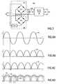
- FIG. 1is a block diagram of an example of an AC-DC power converter in accordance with a first embodiment of the invention.
- FIGS. 2A , 2 B, 2 C and 2 Dare graphs showing the waveforms of the AC line voltage, the output voltage of first rectifying circuit, the output voltage of second rectifying circuit, and the voltage across the DC input of the DC-DC converter in the example of an AC-DC power converter shown in FIG. 1 .
- FIG. 3is a block diagram of an example of an AC-DC power converter in accordance with a second embodiment of the invention.
- FIGS. 4A , 4 B, 4 C and 4 Dare graphs showing the waveforms of the AC line voltage, the output voltage of first rectifying circuit, the output voltage of second rectifying circuit, and the voltage across the DC input of the DC-DC converter in the example of an AC-DC power converter shown in FIG. 3 .
- FIG. 5is a block diagram of an example of an AC-DC power converter in accordance with a third embodiment of the invention.
- FIGS. 6A , 6 B, 6 C and 6 Dare graphs showing the waveforms of the AC line voltage, the output voltage of first rectifying circuit, the output voltage of second rectifying circuit, and the voltage across the DC input of the DC-DC converter in the example of an AC-DC power converter shown in FIG. 5 .
- FIG. 7is a block diagram of an example of an AC-DC power converter in accordance with a fourth embodiment of the invention.
- FIGS. 8A , 8 B, 8 C and 8 Dare graphs showing the waveforms of the AC line voltage, the output voltage of first rectifying circuit, the output voltage of second rectifying circuit, and the voltage across the DC input of the DC-DC converter in the example of an AC-DC power converter shown in FIG. 7 .
- FIG. 9is a block diagram showing an example of an open-loop DC-DC converter that can be used as the DC-DC converter in the above-described embodiments.
- FIG. 10is a block diagram showing a first example of a closed-loop DC-DC converter that can be used as the DC-DC converter in the above-described embodiments.
- FIG. 11is a block diagram showing a second example of a closed-loop DC-DC converter that can be used as the DC-DC converter in the above-described embodiments.
- FIG. 12is a schematic diagram showing an example of an acoustically-coupled transformer that may be used in the DC-DC converter embodiments shown in FIGS. 9 , 10 and 11 .
- FIG. 13is a graph showing the frequency response of the calculated forward transmission coefficient of a typical embodiment of the acoustically-coupled transformer shown in FIG. 12 and the frequency response of the calculated forward transmission coefficient of one of its electro-acoustic transducers over the frequency range from 90 MHz to 210 MHz.
- FIG. 14is a schematic diagram of an exemplary embodiment of the DC-DC converter shown in FIG. 11 and incorporating an embodiment of the acoustically-coupled transformer shown in FIG. 13 .
- FIG. 15is a flow chart showing an example of a first AC-DC power conversion method in accordance with an embodiment of the invention.
- FIG. 16is a flow chart showing an example of a second AC-DC power conversion method in accordance with an embodiment of the invention.
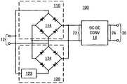
- FIG. 1is a block diagram of an example of an AC-DC power converter 100 in accordance with a first embodiment of the invention.
- AC-DC power converter 100is composed of AC input 12 , a first rectifying circuit 110 , a second rectifying circuit 120 , a DC-DC converter 18 and a DC output 20 .
- DC-DC converterhas a DC input 22 and a DC output 24 .
- First rectifying circuit 110 and second rectifying circuit 120are connected in parallel between AC input 12 and the DC input 22 of DC-DC converter 18 .
- At least one of the rectifying circuitscomprises a phase shifting element that provides a phase shift at the AC line frequency.
- second rectifying circuit 120comprises a phase shifting element 123 .
- First rectifying circuit 110 and second rectifying circuit 120deliver high-voltage raw DC to the DC input 22 of DC-DC converter 18 .
- DC-DC converter 18converts the high-voltage raw DC provided by first rectifying circuit 110 and second rectifying circuit 120 to smooth DC at a lower voltage and delivers the smooth, lower voltage DC to DC output 20 .
- the electronic device (not shown) powered by AC-DC power converter 100is connected to DC output 20 .
- DC-DC converter 18additionally provides galvanic isolation between AC input 12 and DC output 20 at voltage differences typically in the range from about 1 kV to 4 kV.
- DC-DC converter 18has a minimum input voltage.
- the voltage across the DC input 22 of the DC-DC converter falling below the minimum input voltage ofcauses undesirable periodic dips in the DC voltage delivered by the DC-DC converter to DC output 20 . Accordingly, the minimum voltage provided to DC input 22 under maximum load conditions should remain greater than the minimum input voltage of DC-DC converter 18 .
- first rectifying circuit 110is composed of a bridge rectifier 114 having inputs connected to AC input 12 and outputs connected to the DC input 22 of DC-DC converter 18 .
- Second rectifying circuit 120is composed of phase shifting element 123 and a bridge rectifier 124 connected between AC input 12 and the DC input 22 of DC-DC converter 18 . More specifically, phase shifting element 123 is connected between AC input 12 and one input of bridge rectifier 124 , and the outputs of bridge rectifier 124 are connected to the DC input 22 of DC-DC converter 18 .
- phase shifting element 123is embodied as an inductor that imposes a phase lag on the AC current fed from AC input 12 to bridge rectifier 124 .
- FIG. 2Ais a graph showing the waveform 130 of the AC line voltage received at AC input 12 .
- the AC line voltagehas a nominal frequency of 50 Hz or 60 Hz and a nominal RMS voltage in the range from 100 volts to 240 volts.
- FIG. 2Bis a graph showing the waveform 132 of the output voltage of first rectifying circuit 110 .
- the output voltage of the first rectifying circuithas a frequency equal to twice the AC line frequency and a nominal peak voltage in the range from about 140 volts to about 340 volts, depending on the nominal AC line voltage.
- the output voltage of the first rectifying circuitis substantially in phase with the AC line voltage.
- FIG. 2Cis a graph showing the waveform 134 of the output voltage of second rectifying circuit 120 .
- the output voltage of the second rectifying circuithas a frequency equal to twice the AC line frequency and a nominal peak voltage in the range from about 140 volts to about 340 volts, depending on the nominal AC line voltage.
- phase shifting element 123Due to phase shifting element 123 , the output voltage of second rectifying circuit 120 is shifted in phase relative to the AC line voltage and, hence, relative to the output voltage of first rectifying circuit 110 .
- phase shifting element 123introduces a lag, so that the output voltage of rectifying circuit 120 lags the AC line voltage and that of first rectifying circuit 110 by a phase shift ⁇ , as shown in FIG. 2C .
- FIG. 2Dis a graph showing the waveform of the voltage across the DC input 22 of DC-DC converter 18 .
- the waveformis a superposition of above-described waveforms 132 and 134 that differ in phase by a phase shift ⁇ . Operation of AC-DC power converter 100 will be described starting at a time t 0 , which is one of the times at which the output voltage of first rectifying circuit 110 is zero. At time t 0 , the voltage output by first rectifying circuit 110 is less than the voltage output by second rectifying circuit 120 due to the phase lag in the voltage output of the second rectifying circuit.
- second rectifying circuit 120is the sole supplier of current to DC-DC converter 18 : the diodes of first rectifying circuit 110 are reverse biased.
- the output voltage of first rectifying circuit 110increases as the output of second rectifier circuit 120 falls.
- the output voltage of first rectifying circuit 110becomes greater than that of second rectifying circuit 120 , and first rectifying circuit 110 takes over as the sole supplier of current to DC-DC converter 18 .
- the diodes of second rectifying circuit 120are reverse biased.
- the output voltage of first rectifying circuit 110continues to increase to a peak value, then begins to fall as the output voltage of second rectifying circuit 120 rises.
- the output voltage of first rectifying circuit 110falls below that of second rectifying circuit 120 , and second rectifying circuit 120 once more becomes the sole supplier of current to DC-DC converter 18 .
- the process just describedthen repeats every half cycle of the AC line voltage, with the task of sole supplier of current to DC-DC converter 18 alternating between first rectifying circuit 110 and second rectifying circuit 120 at times t 1 and t 2 .
- solid linesare used to indicate the portion of the output voltage waveform 132 of first rectifying circuit 110 and the portion of the voltage waveform 134 of second rectifying circuit 120 during which the respective rectifying circuit is supplying current to DC-DC converter 18 . Additionally, in FIG. 2D , broken lines are used to indicate the portion of the output voltage waveform 132 of first rectifying circuit 110 and the portion of the voltage waveform 134 of second rectifying circuit 120 during which the respective rectifying circuit is not supplying current to DC-DC converter 18 .
- FIG. 2Dillustrates how the voltage across DC input 22 never falls below the minimum voltage level indicated by the line 136 : second rectifying circuit 120 provides to DC-DC converter 18 a voltage greater than minimum voltage level 136 during the time that the output voltage of first rectifying circuit is below minimum voltage level 136 and vice versa.
- Minimum voltage level 136depends on the phase shift provided by phase shifting element 123 .
- Phase shifting element 123is specified such that the phase shift it provides is sufficient to ensure that minimum voltage level 136 is greater than or equal to the minimum input voltage of DC-DC converter 18 at its maximum output current. This will be described below in more detail.
- First rectifying circuit 110 and second rectifying circuit 120collectively maintain the voltage at the DC input 22 of DC-DC converter 18 above the minimum input voltage of DC-DC converter 18 . This prevents undesirable periodic dips in the DC voltage delivered to DC output 20 .
- the peak output voltage of first rectifying circuit 110 and second rectifying circuit 120is about 120 ⁇ 2 volts, i.e., about 170 V.
- the period corresponding to the AC line frequency of 60 Hzis 16.7 milliseconds (ms). This means that the output voltage of each of the first rectifying circuit and the second rectifying circuit falls to zero every 8.3 ms.
- the time ⁇ during which the output of each of the first rectifying circuit and the second rectifying circuit falls below the minimum input voltage of the DC-DC converteris given by:
- the output voltage of first rectifying circuit 110falls below the minimum input voltage of DC-DC converter 18 for a time 0.31 ms every half cycle of the AC line voltage. This time will be referred to as the dead time of first rectifying circuit 110 .
- the output voltage of second rectifying circuitfalls to zero later than that of first rectifying circuit 110 due to the phase lag between the output voltage of the first rectifying circuit and the output voltage second rectifying circuit.
- the phase lagis determined by phase shifting element 123 .
- Phase shifting element 123is specified such that the output voltage of the second rectifying circuit remains greater than the minimum input voltage of DC-DC converter 18 during the dead time (i.e., 0.31 ms in this example). This allows the voltage across the DC input 22 of DC-DC converter 18 to remain above the minimum input voltage of DC-DC converter 18 without the need for an energy storage element, such as a large capacitance, high working voltage electrolytic capacitor.
- phase shifting element 123is designed to provide a phase shift of 6.6 degrees with an effective load resistance of 1 ohm, i.e., phase shifting element 123 is an inductor with a reactance of j*0.058 ohms.
- An inductor of about 380 microhenries ( ⁇ H)has this reactance at 60 Hz.
- Phase shifting element 123may alternatively constitute part of first rectifying circuit 110 .
- phase shifting element 123is connected between AC input 12 and one input of bridge rectifier 114 , and second rectifying circuit 120 comprises no phase shifting element.
- FIG. 3is a block diagram of an example of an AC-DC power converter 200 in accordance with a second embodiment of the invention.
- AC-DC power converter 200is composed of AC input 12 , first rectifying circuit 110 , a second rectifying circuit 220 , DC-DC converter 18 and DC output 20 .
- First rectifying circuit 110 and second rectifying circuit 220are connected in parallel between AC input 12 and the DC input 22 of DC-DC converter 18 .
- At least one of the rectifying circuitscomprises a phase shifting element providing a phase shift at the AC line frequency.
- second rectifying circuit 120comprises a phase shifting element 223 .
- second rectifying circuit 220is composed of phase shifting element 223 and bridge rectifier 124 connected between AC input 12 and the DC input 22 of DC-DC converter 18 . More specifically, phase shifting element 223 is connected between AC input 12 and one input of bridge rectifier 124 , and the outputs of bridge rectifier 124 are connected to the DC input 22 of DC-DC converter 18 . In this embodiment, in second rectifying circuit 220 , phase shifting element 223 is embodied as a capacitor that imposes a phase lead on the AC current fed to bridge rectifier 124 .
- FIG. 4Ais a graph showing the waveform 130 of the AC line voltage received at AC input 12 .
- the AC line voltagehas a nominal frequency of 50 Hz or 60 Hz and a nominal RMS voltage in the range from 100 volts to 240 volts.
- FIG. 4Bis a graph showing the waveform 132 of the output voltage of first rectifying circuit 110 .
- the output voltagehas a frequency equal to twice the AC line frequency and a nominal peak voltage in the range from about 140 volts to 340 volts, depending on the nominal AC line voltage.
- the output voltage of first rectifying circuit 110is substantially in phase with the AC line voltage.
- FIG. 4Cis a graph showing the waveform 234 of the output voltage of second rectifying circuit 220 .
- the output voltage of the second rectifying circuithas a frequency equal to twice the AC line frequency and a nominal peak voltage in the range from about 140 volts to 340 volts, depending on the nominal AC line voltage.
- phase shifting element 223Due to phase shifting element 223 , the output voltage of second rectifying circuit 220 is shifted in phase relative to the AC line voltage and, hence, relative to the output voltage of first rectifying circuit 110 .
- phase shifting element 223introduces a phase lead, so that the output voltage of second rectifying circuit 220 leads the AC line voltage and the output voltage of first rectifying circuit 110 by a phase shift of ⁇ , as shown in FIG. 4C .
- FIG. 4Dis a graph showing the waveform of the voltage across the DC input 22 of DC-DC converter 18 . Operation of AC-DC power converter 200 will be described starting at a time t 0 , which is one of the times at which the output voltage of first rectifying circuit 110 is zero. At time to, the output voltage of second rectifying circuit 220 is greater than the output voltage of first rectifying circuit 110 due to the phase lead in the output voltage of the second rectifying circuit. Thus, second rectifying circuit 220 is the sole supplier of current to DC-DC converter 18 : the diodes of first rectifying circuit 110 are reverse biased.
- the output voltage of second rectifying circuit 220increases to its peak and then falls followed by the increasing and then falling output voltage of first rectifying circuit 110 .
- the output voltage of second rectifying circuit 220falls below that of first rectifying circuit 110 , and first rectifying circuit 110 becomes the sole supplier of current to DC-DC converter 18 .
- the diodes of second rectifying circuit 220are reverse biased. Later, the output voltage of second rectifying circuit 220 falls to zero, and then starts to rise. During this time, the output voltage of first rectifying circuit 110 remains greater than or equal to minimum voltage level 136 .
- first rectifying circuit 110Eventually, at time t 2 , the output voltage of second rectifying circuit 220 once more exceeds the output voltage of first rectifying circuit 110 , and second rectifying circuit takes over once more as the sole supplier of current to DC-DC converter 18 .
- the diodes of first rectifying circuit 110are reverse biased. The process just described then repeats every half cycle of the AC line voltage, with first rectifying circuit 110 and second rectifying circuit 220 alternating at times t 1 and t 2 as the sole supplier of current to DC-DC converter 18 .
- solid linesare used to indicate the portion of the output voltage waveform 132 of first rectifying circuit 110 and the portion of the voltage waveform 234 of second rectifying circuit 220 during which the respective rectifying circuit is supplying current to DC-DC converter 18 . Additionally, in FIG. 4D , broken lines are used to indicate the portion of the output voltage waveform 132 of first rectifying circuit 110 and the portion of the voltage waveform 234 of second rectifying circuit 220 during which the respective rectifying circuit is not supplying current to DC-DC converter 18 .
- FIG. 4Dillustrates how the voltage across DC input 22 never falls below the minimum voltage level indicated by the line 136 : first rectifying circuit 110 provides to DC-DC converter 18 a voltage greater than minimum voltage level 136 during the time that the output voltage of second rectifying circuit 220 is below minimum voltage level 136 and vice versa.
- Minimum voltage level 136depends on the phase shift provided by phase shifting element 223 .
- Phase shifting element 223is specified such that the phase shift it provides is sufficient to ensure that minimum voltage level 136 is greater than or equal to the minimum input voltage of DC-DC converter 18 at its maximum output current.
- First rectifying circuit 110 and second rectifying circuit 220collectively maintain the voltage at the DC input 22 of DC-DC converter 18 above the minimum input voltage of DC-DC converter 18 . This prevents undesirable periodic dips in the DC voltage delivered to DC output 20 .
- a capacitance of about 33 millifarads (33 mF)has the above-stated reactance of ⁇ j*0.058 ohms.
- the maximum voltage across the capacitoris small, so the capacitor need have only a small working voltage.
- Phase shifting element 223may alternatively constitute part of first rectifying circuit 110 .
- phase shifting element 223is connected between AC input 12 and one input of bridge rectifier 114 , and second rectifying circuit 220 comprises no phase shifting element.
- FIG. 5is a block diagram of an example of an AC-DC power converter 300 in accordance with a third embodiment of the invention.
- AC-DC power converter 300is composed of AC input 12 , a first rectifying circuit 310 , a second rectifying circuit 320 , DC-DC converter 18 and DC output 20 .
- First rectifying circuit 310 and second rectifying circuit 320are connected in parallel between AC input 12 and the DC input 22 of DC-DC converter 18 .
- Rectifying circuits 310 and 320each comprise a phase shifting element providing a phase shift at the AC line frequency.
- first rectifying circuit 310comprises a phase shifting element 313
- second rectifying circuit 320comprises a phase shifting element 323 .
- Phase shifting elements 313 and 323provide opposite and substantially equal phase shifts.
- first rectifying circuit 310is composed of phase shifting element 313 and bridge rectifier 114 connected between AC input 12 and the DC input 22 of DC-DC converter 18 . More specifically, phase shifting element 313 is connected between AC input 12 and one input of bridge rectifier 114 , and the outputs of bridge rectifier 114 are connected to the DC input 22 of DC-DC converter 18 .
- Second rectifying circuit 320is composed of phase shifting element 323 and bridge rectifier 124 connected between AC input 12 and the DC input 22 of DC-DC converter 18 . More specifically, phase shifting element 323 is connected between AC input 12 and one input of bridge rectifier 124 , and the outputs of bridge rectifier 124 are connected to the DC input 22 of DC-DC converter 18 .
- phase shifting element 313is embodied as a capacitor that imposes a phase lead on the AC current fed from AC input 12 to bridge rectifier 114 and, in second rectifying circuit 320 , phase shifting element 323 is embodied as an inductor that imposes a phase lag on the AC current fed from AC input 12 to bridge rectifier 124 .
- FIG. 6Ais a graph showing the waveform 130 of the AC line voltage received at AC input 12 .
- the AC line voltagehas a nominal frequency of 50 Hz or 60 Hz and a nominal RMS voltage in the range from 100 volts to 240 volts.
- FIG. 6Bis a graph showing the waveform 332 of the output voltage of first rectifying circuit 110 .
- the output voltage of the first rectifying circuithas a frequency equal to twice the AC line frequency and a nominal peak voltage in the range from about 140 volts to about 340 volts, depending on the nominal AC line voltage.
- phase shifting element 313Due to phase shifting element 313 , the output voltage of first rectifying circuit 110 is shifted in phase relative to the AC line voltage. In the example shown, phase shifting element 313 introduces a phase lead, so that the output voltage of first rectifying circuit 310 leads the AC line voltage by a phase shift ⁇ /2, as shown in FIG. 6B .
- FIG. 6Cis a graph showing the waveform 334 of the output voltage of second rectifying circuit 320 .
- the output voltage of the second rectifying circuithas a frequency equal to twice the AC line frequency and a nominal peak voltage in the range from about 140 volts to about 340 volts, depending on the nominal AC line voltage.
- phase shifting element 323Due to phase shifting element 323 , the output voltage of second rectifying circuit 320 is shifted in phase relative to the AC line voltage. In the example shown, phase shifting element 323 introduces a phase lag, so that the output voltage of rectifying circuit 320 lags that of the AC line voltage by a phase shift ⁇ /2, as shown in FIG. 6C .
- FIG. 6Dis a graph showing the waveform of the voltage across the DC input 22 of DC-DC converter 18 .
- the waveformis a superposition of above-described waveforms 332 and 334 that differ in phase by a phase shift ⁇ . Operation of AC-DC power converter 300 will be described starting at a time t 0 , which is one of the times at which the output voltage of first rectifying circuit 310 is zero. At time t 0 , the output voltage of first rectifying circuit 310 is less than the output voltage of second rectifying circuit 320 due to the phase lag between the output voltage of the second rectifying circuit and that of the first rectifying circuit.
- second rectifying circuit 320is the sole supplier of current to DC-DC converter 18 : the diodes of first rectifying circuit 310 are reverse biased. As time advances from time t 0 , the output voltage of first rectifying circuit 310 increases as the output of second rectifying circuit 320 falls. At time t 1 , the output voltage of first rectifying circuit 310 becomes greater than that of second rectifying circuit 320 , and first rectifying circuit 310 takes over as the sole supplier of current to DC-DC converter 18 . The diodes of second rectifying circuit 320 are reverse biased. The output voltage of first rectifying circuit 310 continues to increase to a peak value, then begins to fall as the output voltage of second rectifying circuit 320 continues to rise.
- first rectifying circuit 310falls below that of second rectifying circuit 320 , and second rectifying circuit 320 once more becomes the sole supplier of current to DC-DC converter 18 .
- the process just describedthen repeats every half cycle of the AC line voltage, with first rectifying circuit 310 and second rectifying circuit 320 alternating at times t 1 and t 2 as the sole supplier of current to DC-DC converter 18 .
- solid linesare used to indicate the portion of the output voltage waveform 332 of first rectifying circuit 310 and the portion of the voltage waveform 334 of second rectifying circuit 320 during which the respective rectifying circuit is supplying current to DC-DC converter 18 . Additionally, in FIG. 6D , broken lines are used to indicate the portion of the output voltage waveform 332 of first rectifying circuit 310 and the portion of the voltage waveform 334 of second rectifying circuit 320 during which the respective rectifying circuit is not supplying current to DC-DC converter 18 .
- FIG. 6Dillustrates how the voltage across DC input 22 never falls below the minimum voltage level indicated by the line 136 : second rectifying circuit 320 provides to DC-DC converter 18 a voltage greater than minimum voltage level 136 during the time that the output voltage of first rectifying circuit 310 is below minimum voltage level 136 and vice versa.
- Minimum voltage level 136depends on the phase shift between the output voltages of first rectifying circuit 310 and second rectifying circuit 320 collectively provided by phase shifting element 313 and phase shifting element 323 .
- Phase shifting elements 313 and 323are specified such that the phase shift they collectively provide is sufficient to ensure that minimum voltage level 136 is greater than or equal to the minimum input voltage of DC-DC converter 18 at its maximum output current.
- First rectifying circuit 310 and second rectifying circuit 320collectively maintain the voltage at the DC input 22 of DC-DC converter 18 above the minimum input voltage of DC-DC converter 18 . This prevents undesirable periodic dips in the DC voltage that DC-DC converter 18 delivers to DC output 20 .
- phase shifting element 313is a capacitor and phase shifting element 323 is an inductor
- each phase shifting elementprovides approximately one half of the total phase shift between the output voltages of first rectifying circuit 310 and second rectifying circuit 320 . Consequently, phase shifting element 313 has a capacitance of about one half of that of phase shifting element 223 described above with reference to FIG. 3 , and a similar working voltage.
- Phase shifting element 323has an inductance of about one half of that of phase shifting element 123 described above with reference to FIG. 1 .
- phase shifting element 313may alternatively be an inductor that imposes a phase lag on the AC line current.
- phase shifting element 323may alternatively be a capacitor that imposes a phase lead on the AC line current.
- a filter capacitormay be located in parallel with the DC input 22 of DC-DC converter 18 .
- a relatively small filter capacitorwill principally remove switching transients and AC line glitches from the raw DC provided to DC-DC converter 18 .
- a substantially larger filter capacitorwill principally decrease the dynamic range and increase the minimum voltage of the raw DC provided to the DC-DC converter.
- FIG. 7is a block diagram of an example of an AC-DC power converter 400 in accordance with a fourth embodiment of the invention.
- AC-DC power converter 400is composed of AC input 12 , first rectifying circuit 110 , second rectifying circuit 120 , a filter capacitor 416 , DC-DC converter 18 and DC output 20 .
- DC-DC converterhas a DC input 22 and a DC output 24 .
- First rectifying circuit 110 and second rectifying circuit 120are connected in parallel between AC input 12 and the DC input 22 of DC-DC converter 18 .
- Filter capacitor 416is connected in parallel with DC input 22 .
- At least one of the rectifying circuitscomprises a phase shifting element providing a phase shift at the AC line frequency.
- second rectifying circuit 120comprises phase shifting element 123 and phase shifting element 123 is an inductor providing a phase lag.
- FIGS. 8A , 8 B, and 8 Care graphs showing the waveform 130 of the AC line voltage received at AC input 12 , the waveform 132 of the output voltage of first rectifying circuit 110 and the waveform 134 of the output voltage of second rectifying circuit 120 .
- the above description of FIGS. 2A , 2 B and 2 Capplies to FIGS. 8A , 8 B, and 8 C, respectively, so FIGS. 8A , 8 B, and 8 C will not be individually described.
- FIG. 8Dis a graph showing the waveform of the voltage across the DC input 22 of DC-DC converter 18 and across filter capacitor 416 . Operation of AC-DC power converter 400 will be described starting at a time t 0 , which is one of the times at which the output voltage of first rectifying circuit 110 is zero. At time t 0 , the output voltage of first rectifying circuit 110 and the output voltage of second rectifying circuit 120 are both less than the voltage on filter capacitor 416 . Thus, filter capacitor 416 is the sole supplier of current to DC-DC converter 18 : the diodes of first rectifying circuit 110 and the diodes of second rectifying circuit 120 are reverse biased.
- first rectifying circuit 110supplies current to filter capacitor 416 , so that the voltage on the filter capacitor follows the output voltage of first rectifying circuit 110 .
- the diodes of second rectifying circuit 120remain reverse biased.
- the output voltage of first rectifying circuit 110continues to increase to a peak value, then begins to fall as the output voltage of second rectifying circuit 120 continues to rise.
- Filter capacitoralso discharges as the output voltage of first rectifying circuit 110 falls.
- the output voltage of first rectifying circuit 110falls below that of second rectifying circuit 120 , and second rectifying circuit 120 becomes the sole supplier of current to DC-DC converter 18 .
- second rectifying circuit 120supplies current to filter capacitor 416 , so that the voltage on the filter capacitor follows the output voltage of second rectifying circuit 120 .
- the output voltage of second rectifying circuit 120falls, eventually falling faster than the voltage on filter capacitor 416 .
- Second rectifying circuit 120At time t 3 , the diodes of second rectifying circuit 120 become reverse biased, second rectifying circuit 120 stops supplying current to DC-DC converter 18 , and filter capacitor 416 takes over as the sole supplier of current to DC-DC converter 18 . Filter capacitor 416 remains the sole supplier of current to DC-DC converter 18 until time t 1 of the next half cycle of the AC line voltage.
- FIG. 8Dsolid lines are used to indicate the portion of the output voltage waveform 132 of first rectifying circuit 110 , the portion of the voltage waveform 134 of second rectifying circuit 120 and the portion of the voltage waveform of filter capacitor 416 during which the respective rectifying circuit or filter capacitor is supplying current to DC-DC converter 18 . Additionally, in FIG. 8D , broken lines are used to indicate the portion of the output voltage waveform 132 of first rectifying circuit 110 and the portion of the voltage waveform 134 of second rectifying circuit 120 during which the respective rectifying circuit is not supplying current to DC-DC converter 18 .
- FIG. 8Dillustrates how the voltage across DC input 22 never falls below the minimum voltage level indicated by the line 436 : second rectifying circuit 120 and filter capacitor 416 collectively provide to DC-DC converter 18 a voltage greater than minimum voltage level 436 during the time that the output voltage of first rectifying circuit 110 is below minimum voltage level 436 . Additionally, first rectifying circuit 110 and filter capacitor 416 collectively provide to DC-DC converter 18 a voltage greater than minimum voltage level 436 during the time that the output voltage of second rectifying circuit 120 is below minimum voltage level 436 .
- Minimum voltage level 436depends on the phase shift provided by phase shifting element 123 and the capacitance of filter capacitor 416 .
- Phase shifting element 123 and filter capacitor 416are specified such that minimum voltage level 436 is greater than or equal to the minimum input voltage of DC-DC converter 18 at its maximum output current.
- phase shifting element 123 in AC-DC power converter 400can be specified to give less phase shift than in AC-DC power converter 100 described above with reference to FIG. 1 .
- DC-DC converter 18Many different types of DC-DC converters that provide galvanic isolation are known in the art and may be used as DC-DC converter 18 .
- Some examples of DC-DC converters suitable for use as DC-DC converter 18will be described next with reference to FIGS. 9-14 . The examples will be described with reference to their application to AC-DC power converter 100 described above with reference to FIG. 1 . The examples may equally well be applied to AC-DC power converters 200 , 300 and 400 described above with reference to FIGS. 3 , 5 and 7 , respectively.
- FIG. 9is a block diagram showing an example 500 of an open-loop DC-DC converter that can be used as DC-DC converter 18 .
- DC-DC converter 500is composed of an inverter 502 , an acoustically-coupled transformer 504 and a rectifier and filter circuit 506 .
- Inverter 502has an input connected to the DC input 22 of DC-DC converter 500 and an output connected to the primary of acoustically-coupled transformer 504 .
- the secondary of acoustically-coupled transformer 504is connected to the input of rectifier and filter circuit 506 .
- the output of rectifier and filter circuit 506is connected to DC output 24 .
- Inverter 502receives the raw DC power output by first rectifying circuit 110 and second rectifying circuit 120 and generates AC power from the raw DC.
- the AC poweris typically a sine-wave or square wave at a frequency in the order of 100 MHz.
- Acoustically-coupled transformer 504passes the AC power but blocks DC and extraneous AC up to the specified breakdown voltage of AC-DC power converter 100 ( FIG. 1 ). As noted above, the breakdown voltage is typically in the range from about 1 kV to 4 kV. Acoustically-coupled transformer 504 additionally steps the voltage of the AC power down to a voltage more similar to the rated output voltage of AC-DC power converter 100 .
- Rectifier and filter circuit 506rectifies the stepped-down AC power output by acoustically-coupled transformer 504 and filters the residual AC from the resulting DC power. Because the DC power output by the rectifier has a substantial AC component at twice the AC line frequency, the rectifier and filter circuit typically comprises a filter capacitor having a relatively large capacitance. However, the voltage rating of the filter capacitor is relatively low since it is on the secondary side of acoustically-coupled transformer 504 , so the physical size of the capacitor need not be large. Additionally, in this open-loop embodiment, rectifier and filter circuit 506 may incorporate a DC regulator to regulate the DC voltage provided to DC output 24 .
- FIGS. 10 and 11Two examples of a closed-loop DC-DC converter that can be used as DC-DC converter 18 will be described next with reference to FIGS. 10 and 11 .
- the two exampleshave the same forward path but differ in their feedback circuits.
- FIG. 10shows a first example 550 of a closed-loop DC-DC converter that can be used as DC-DC converter 18 .
- DC-DC converter 550is composed of an inverter 552 , acoustically-coupled transformer 504 , a rectifier and filter circuit 556 and a feedback circuit 560 that extends between DC output 24 and a control input of inverter 552 .
- Inverter 552 , acoustically-coupled transformer 504 and rectifier and filter circuit 556are connected between DC input 22 and DC output 24 in a manner similar to that described above with reference to inverter 502 , acoustically-coupled transformer 504 and rectifier and filter circuit 506 shown in FIG. 9 .
- Feedback circuit 560is composed of a comparator 562 , a galvanic isolator 564 and a controller 566 connected in series.
- Comparator 562receives the DC voltage across DC output 24 , compares this voltage with a reference voltage V REF and generates an error signal representing the difference between the DC voltage and the reference voltage.
- the comparatorpasses the error signal to galvanic isolator 564 .
- Galvanic isolator 564passes the error signal to controller 566 but blocks DC and extraneous AC up to the specified breakdown voltage of AC-DC power converter 100 ( FIG. 1 ).
- Controller 566receives the error signal and, from the error signal, generates a control signal suitable for controlling the output of inverter 552 .
- the control signal output by controller 566controls the output of inverter 552 in a manner that tends to correct the error represented by the error signal.
- the control signaloperates to hold the DC voltage across DC output 24 constant notwithstanding the large voltage range of the raw DC power received at DC input 22 .
- Thisremoves most of the AC component at twice the line frequency from the DC power output by the rectifier and allows filtering to be performed by a filter capacitor having a capacitance of the order of nanofarads.
- a filter capacitorhas is substantially smaller in physical size than the filter capacitor that constitutes part of rectifier and filter circuit 506 described above with reference to FIG. 9 .
- controller 566constitutes part of inverter 552 , and inverter receives the error signal from galvanic isolator 564 .
- Galvanic isolators based on optical coupling or magnetic couplingare known in the art and may be used galvanic isolator 564 .
- An acoustic galvanic isolatormay also be used as galvanic isolator 564 .
- acoustic galvanic isolators based on film bulk acoustic resonators (FBARs)may be used, such as those disclosed by Larson et al. in U.S. patent application Ser. No. 11/253,464, entitled Acoustic Galvanic Isolator, assigned to the assignee of this disclosure and incorporated by reference.
- galvanic isolator 564is an acoustic galvanic isolator that shares common components and operates at the same frequency as acoustically-coupled transformer 504 .
- comparator 562has a signal input connected to DC output 24 and a clock input connected to receive a sample of the AC power output by acoustically-coupled transformer 504 .
- the comparatorgenerates an error signal and modulates the clock signal with the error signal to generate an RF error signal and the same frequency as the AC power coupled by acoustically-coupled transformer 504 .
- Acoustic galvanic isolator 564passes the RF error signal to controller 566 but blocks DC and extraneous AC up to the specified breakdown voltage of AC-DC power converter 100 ( FIG. 1 ).
- Controller 566receives the RF error signal, demodulates the error signal from the RF error signal and generates from the error signal a control signal suitable for controlling the output of inverter 552 as described above.
- controllermay provide the error signal itself to the inverter as the control signal.
- the controllermay constitute part of inverter 552 , in which case inverter 552 receives the RF error signal from acoustic galvanic isolator 564 .
- Other types of galvanic isolators capable of operating at RFmay be used as element 564 in DC-DC converter 550 .
- FIG. 11shows a second example 570 of a closed-loop DC-DC converter that can be used as DC-DC converter 18 .
- DC-DC converter 570is composed of inverter 552 , acoustically-coupled transformer 504 , rectifier and filter circuit 556 and a feedback circuit 580 that extends between DC output 24 and the control input of inverter 552 .
- Inverter 552 , acoustically-coupled transformer 504 , rectifier and filter circuit 556 and feedback circuit 580are interconnected in a manner similar to that described above with reference to inverter 552 , acoustically-coupled transformer 504 rectifier and filter circuit 556 and feedback circuit 560 shown in FIG. 10 .
- Feedback circuit 580is composed of a modulator 582 , galvanic isolator 564 and a controller 586 connected in series.
- Modulator 582receives the DC voltage output by first rectifying circuit 556 and a sample of the AC voltage output by acoustically-coupled transformer 504 to generate an RF voltage signal representing the DC voltage output by DC-DC converter 570 .
- the modulatorpasses the RF voltage signal to galvanic isolator 564 .
- Galvanic isolator 564passes the RF voltage signal to controller 566 but blocks DC and extraneous AC up to the specified breakdown voltage of AC-DC power converter 100 ( FIG. 1 ).
- Controller 586receives the RF voltage signal and demodulates the RF voltage signal to recover the voltage signal representing the DC voltage output by DC-DC converter 570 . Controller 586 compares the voltage signal with a reference voltage V REF to generate an error signal that it feeds to the control input of inverter 562 . The error signal controls the output of inverter 552 in a manner that tends to correct the error represented by the error signal, as described above.
- galvanic isolator 564is an acoustic galvanic isolator.
- FIG. 12is a schematic diagram showing an example of an acoustically-coupled transformer 600 that may be used as acoustically-coupled transformer 504 in the exemplary embodiments of DC-DC converter 18 shown in FIGS. 9 , 10 and 11 .
- Acoustically-coupled transformer 600is implemented as a resonant structure 621 having at least one mechanical resonance in an operating frequency range.
- the center frequency of the operating frequency rangeis in the frequency range from about 20 MHz to about 500 MHz.
- a typical center frequency of the operating frequency rangeis about 150 MHz.
- the frequency of the AC power output by inverter 552is nominally equal to the center frequency.
- Resonant structure 621is composed of an insulating substrate 630 , a first electro-acoustic transducer 640 and a second electro-acoustic transducer 650 .
- Substrate 630has a first major surface 632 and a second major surface 634 opposite first major surface 632 .
- First electro-acoustic transducer 640is mechanically coupled to the first major surface 632 of the substrate 630 .
- Second electro-acoustic transducer 650is mechanically coupled to the second major surface 634 of substrate 630 .
- insulating substrate 630examples include alumina, glass, ceramic, sapphire and one or more other electrically-insulating materials having a high resistivity and a high electrical breakdown field.
- insulating substrate 630is composed of one or more layers of an at least partially electrically-conducting material, such as silicon, and one or more layers of electrically-insulating material having a high resistivity and a high electrical breakdown field. Insulating substrate 630 electrically isolates first electro-acoustic transducer 640 from second electro-acoustic transducer 650 at voltages up to the specified breakdown voltage of AC-DC power converter 100 ( FIG. 1 ).
- Electro-acoustic transducers 640 and 650are located on the opposed major surfaces of substrate 630 . Each of the transducers 640 and 650 is operable to convert input AC electrical power to acoustic energy and to convert acoustic energy to output AC electrical power.
- Resonant structure 621including substrate 630 and electro-acoustic transducers 640 and 650 , is structured to resonate mechanically at least one resonant frequency in the operating frequency range of acoustically-coupled transformer 600 .
- resonant structure 621has more than one resonant frequency in the operating frequency range, as will be described in more detail with reference to FIG. 13 .
- first electro-acoustic transducer 640has a first electrode 642 located adjacent substrate 630 , a second electrode 644 opposite first electrode 642 , and a piezoelectric element 646 between first electrode 642 and second electrode 644 .
- Examples of the material of electrodes 642 and 644include gold (Au), platinum (Pt), iridium (Ir), ruthenium (Ru), palladium (Pd), and one or more other electrically-conducting materials.
- Electrodes 642 and 644are electrically connected to AC input terminals 613 of the acoustically-coupled transformer 600 .
- piezoelectric element 646examples include lead zirconium titanate Pb(Zr,Ti)O 3 (PZT), barium titanate (BaTiO 3 ), potassium niobate (KNbO 3 ) and any other piezoelectric material having high electro-acoustic coupling and a high dielectric constant.
- PZTlead zirconium titanate
- BaTiO 3barium titanate
- KNbO 3potassium niobate
- the dimensions and total mass of first electro-acoustic transducer 640for example its thickness 641 , depend on factors such as the operating frequency.
- Second electro-acoustic transducer 650has a first electrode 652 adjacent substrate 630 , a second electrode 654 opposite first electrode 652 , and a piezoelectric element 656 between first electrode 652 and second electrode 654 .
- Examples of the material of electrodes 652 and 654include gold (Au), platinum (Pt), iridium (Ir), ruthenium (Ru), palladium (Pd), and one or more other electrically-conducting materials.
- Electrodes 652 and 654are electrically connected to the AC output terminals 615 of acoustically-coupled transformer 600 .
- piezoelectric element 656examples include lead zirconium titanate Pb(Zr,Ti)O 3 (PZT), barium titanate (BaTiO 3 ), potassium niobate (KNbO 3 ) and any other piezoelectric material having high electro-acoustic coupling and a high dielectric constant.
- PZTlead zirconium titanate
- BaTiO 3barium titanate
- KNbO 3potassium niobate
- the dimensions and total mass of second electro-acoustic transducer 650depend on factors such as the operating frequency.
- First electro-acoustic transducer 640 and second electro-acoustic transducer 650are typically structured to have a mechanical resonance at a frequency nominally equal to the operating frequency. However, as will be described in more detail below with reference to FIG. 13 , the mechanical resonances of the electro-acoustic transducers are substantially lower in Q than the resonances of resonant structure 621 . Specifically, the thickness 641 of first electro-acoustic transducer 640 is an integral multiple of one-half the wavelength in the electro-acoustic transducer of an acoustic wave nominally equal in frequency to the operating frequency.
- the thickness 641can be approximated as follows.
- the speed of sound in PZTis approximately 4,500 meters per second.
- the wavelength of an acoustic wave in the piezoelectric element 646 of first electro-acoustic transducer 640is approximately 30 micrometers ( ⁇ m), calculated as follows: (4.5 ⁇ 10 3 m ⁇ s ⁇ 1 )/(1.5 ⁇ 10 8 s ⁇ 1 )
- first electro-acoustic transducer 650is fabricated with piezoelectric element 646 having a thickness of, for example, somewhat less than 15 ⁇ m.
- the overall thickness 641 of first electro-acoustic transducer 640is, for example, approximately 15 ⁇ m to 40 ⁇ m.
- Lateral dimensions 643 of first electro-acoustic transducer 640are in the range from a few hundred micrometers to a few thousand micrometers, for example, 300 ⁇ m to 3,000 ⁇ m.
- Second electro-acoustic transducer 650is similar in dimensions.
- Inverter 552( FIGS. 10 and 11 ) supplies AC electrical power to AC input terminals 613 .
- First electro-acoustic transducer 640converts the AC power to acoustic energy, i.e., mechanical vibrations.
- the acoustic energycauses resonant structure 621 to vibrate mechanically at the operating frequency.
- the frequency of the AC poweris at or near the frequency of one of the resonances of resonant structure 621 .
- first electro-acoustic transducer 640and second electro-acoustic transducer 650 collectively determine the resonant frequencies of resonant structure 621
- the resonant frequenciesare primarily determined by the thickness of substrate 630 and the speed of sound in the material of the substrate. Accordingly, the thickness and material of substrate 630 primarily determine the frequencies of the mechanical resonances of resonant structure 621 .
- the operating frequency range of inverter 552( FIGS. 10 and 11 ) is chosen to encompass one of the resonant frequencies of resonant structure 621 .
- the operating frequency rangeis chosen so that it includes an operating frequency at which the thickness 631 of substrate 630 is an integral multiple of one-half of the wavelength in the substrate of an acoustic wave nominally equal in frequency to the operating frequency.
- the speed of sound in aluminais approximately 11,000 meters per second.
- the wavelength in substrate 630 of an acoustic wave having a frequency nominally equal to the operating frequencyis approximately 73 ⁇ m, calculated as follows: (11 ⁇ 10 3 m ⁇ s ⁇ 1 )/(1.5 ⁇ 10 8 s ⁇ 1 )
- substrate 630has a thickness 31 that is an integral multiple of (73/2) ⁇ m, e.g., 290 ⁇ m, corresponding to eight half wavelengths.
- substrate 630has a thickness 631 in the order of one hundred micrometers.
- the acoustic energy generated by first electro-acoustic transducer 640is coupled to substrate 630 and causes resonant structure 621 to resonate, i.e., to vibrate mechanically. Continued application of AC power to first electro-acoustic transducer 640 causes resonant structure 621 to accumulate acoustic energy. The mechanical vibration of resonant structure 621 is coupled to second electro-acoustic transducer 650 . Second electro-acoustic transducer 650 absorbs acoustic energy from resonant structure 621 , converts the acoustic energy to electrical energy, and delivers the electrical energy to output terminals 615 as output AC power.
- the output AC power generated by acoustically-coupled transformer 600depends on various factors including the frequency of the input AC power relative to the resonant frequency of resonant mechanical structure 621 .
- FIG. 13is a graph that includes a curve 627 that shows the frequency response of the calculated forward transmission coefficient of a typical embodiment of acoustically-coupled transformer 600 over an exemplary frequency range from 90 MHz to 210 MHz.
- the forward transmission coefficient of acoustically-coupled transformer 600is the ratio of the output AC power output by second electro-acoustic transducer 650 to the input AC power applied to first electro-acoustic transducer 640 .
- the forward transmission coefficients of the first and second electro-acoustic transducers 640 and 650were assumed to remain constant over the indicated frequency range to enable FIG. 13 to show the frequency response of resonant mechanical structure 621 . Due to the multiple mechanical resonances of resonant mechanical structure 621 , the forward transmission coefficient is greater at certain operating frequencies, such as 155 MHz, than at other operating frequencies, such as 144 MHz. The forward transmission coefficient has a peak at the resonant frequencies of resonant mechanical structure 621 . Because the forward transmission coefficient has peaks at multiple frequencies, acoustically-coupled transformer 600 is said to have multi-mode operating characteristic.
- FIG. 13also includes a curve 629 that shows the frequency response of the calculated forward transmission coefficient of a typical embodiment of first electro-acoustic transducer 640 .
- the forward transmission characteristic of second electro-acoustic transducer 650has a similar frequency response.
- the calculated forward transmission coefficient of first electro-acoustic transducer 640is the ratio of the acoustic power generated by first electro-acoustic transducer 640 to the input AC electrical power applied to first electro-acoustic transducer 640 .
- the frequency response of the forward transmission coefficient of first electro-acoustic transducer 640is typical of a resonant device having a Q substantially lower than the Q of the resonances of resonant mechanical structure 621 .
- the operating frequencyto be varied over a frequency range, e.g., from 144 MHz to 155 MHz, that causes a substantial change in the forward transmission coefficient of acoustically-coupled transformer 600 but that causes little variation in the forward transmission coefficients of electro-acoustic transducers 640 and 650 .
- FIG. 13shows how the AC power coupled from input terminals 613 to output terminals 615 may be changed substantially by changing the operating frequency of acoustically-coupled transformer 600 .
- the operating frequency of acoustically-coupled transformer 600is changed by changing the operating frequency of inverter 552 ( FIGS. 10 and 11 ).
- the operating frequencycorresponds to a low forward transmission coefficient
- the operating frequencycorresponds to a high forward transmission coefficient to maintain the voltage at DC output 24 constant.
- Acoustically-coupled transformer 600is described in much more detail, including practical embodiments and fabrication techniques, by John D. Larson III et al. in U.S. patent application Ser. No. 10/971,169 assigned to the assignee of this disclosure and incorporated by reference.
- FIG. 14is a schematic diagram of an exemplary embodiment of DC-DC converter 570 described above with reference to FIG. 11 and incorporating an embodiment of acoustically-coupled transformer 600 described above with reference to FIGS. 12 and 13 .
- the various blocks of DC-DC converter 570 described above with reference to FIG. 11are shown enclosed by broken lines.
- DC-DC converter 570receives the raw DC power output by first rectifying circuit 110 and second rectifying circuit 120 at its DC input 22 .
- inverter 552is composed of a variable-frequency clock signal generator 522 and switching transistors 524 , 525 , 526 and 527 .
- Switching transistors 524 , 525 , 526 and 527are connected as a bridge circuit between DC input 22 and the electrodes 642 and 644 of electro-acoustic transducer 640 that forms part of acoustically-coupled transformer 600 .
- switching transistor 524is connected between one terminal of DC input 22 and electrode 642
- switching transistor 525is connected between the one terminal of DC input 22 and electrode 644
- switching transistor 526is connected between the other terminal of DC input 22 and electrode 642
- switching transistor 527is connected between the other terminal of DC input 22 and electrode 644 .
- Acoustically-coupled transformer 600presents a substantially capacitative load.
- the bridge configuration of switching transistors 524 , 525 , 526 and 527allows the raw DC at DC input 22 both to drive electrical charge into, and to remove electrical charge from, first electro-acoustic transducer 640 .
- Clock signal generator 522generates a clock signal in the operating frequency range of acoustically-coupled transformer 600 .
- the operating frequency rangeextends from about 144 MHz to about 155 MHz. Other frequency ranges are possible.
- Clock signal generatorincorporates driver circuits (not shown) that generate antiphase drive signals suitable for driving switching transistors 524 , 525 , 526 and 527 .
- the gates of switching transistors 524 , 525 , 526 and 527are connected to receive respective drive signals clock signal generator 522 .
- the drive signals received by switching transistors 524 and 527are in antiphase with the drive signals received by switching transistors 525 and 526 .
- switching transistors 524 , 525 , 526 and 527alternate the sense in which electro-acoustic transducer 640 is connected to DC input 22 at the frequency of clock signal generator 522 , i.e., at about 150 MHz.
- Acoustically-coupled transformer 504is embodied as acoustically-coupled transformer 600 substantially as described above with reference to FIG. 12 . However, an additional acoustically-coupled transformer 700 shares substrate 630 with acoustically-coupled transformer 600 . Acoustically-coupled transformer 700 provides galvanic isolator 564 and will be described in detail below.
- Rectifier and filter circuit 556is composed of bridge rectifier 530 and filter capacitor 532 .
- the inputs of bridge rectifier 530are connected to the electrodes 652 and 654 of second electro-acoustic transducer 650 .
- the outputs of bridge rectifier 530are connected to DC output 24 .
- Filter capacitor 532is connected in parallel with DC output 24 .
- the high operational frequency of acoustically-coupled transformer 504allows filter capacitor 532 to have a low capacitance, typically of the order of nanofarads. Low-voltage capacitors of this capacitance are physically small.
- DC output 24is connected to the information signal input of modulator 582 .
- Electrodes 652 and 654 of second electro-acoustic transducer 650are connected to the carrier signal input of modulator 582 .
- Modulator 582modulates the carrier signal provided by electro-acoustic transducer 650 in accordance with the DC voltage across DC output 24 to generate an RF voltage signal that the modulator applies between the electrodes 752 and 754 of the second electro-acoustic transducer 750 of acoustically-coupled transformer 700 .
- Any suitable analog or digital modulation scheme compatible with the properties of the transmission path through acoustically-coupled transformer 700may be used.
- an FM modulation schemein which the frequency of the carrier signal is modulated in accordance with the DC voltage on DC output 24 , may be used.
- the DC voltage across DC output 24may be digitized by an analog-to-digital converter. The amplitude of the carrier signal is then modulated using the output of the analog-to-digital converter.
- Acoustically-coupled transformer 700is similar in structure to acoustically-coupled transformer 600 and shares substrate 630 with acoustically-coupled transformer 600 .
- Acoustically-coupled transformer 700is composed of a first electro-acoustic transducer 740 and a second electro-acoustic transducer 750 located opposite one another on the opposed major surfaces of substrate 630 on the same sides of insulating substrate 630 as first electro-acoustic transducer 640 and second electro-acoustic transducer 650 , respectively.
- Electro-acoustic transducer 740 , electro-acoustic transducer 750 and substrate 630collectively constitute a resonant structure 721 that has a frequency response similar to that of resonant structure 621 described above with reference to FIG. 12 .
- Thisprovides acoustically-coupled transformer 700 with a frequency response similar to that of acoustically-coupled transformer 600 .
- electro-acoustic transducers 740 and 750can be substantially smaller in area than the electro-acoustic transducers of acoustically-coupled transformer 600 .
- First electro-acoustic transducer 740is composed of a first electrode 742 adjacent substrate 630 , a second electrode 744 opposite first electrode 742 , and a piezoelectric element 746 between electrodes 742 and 744 .
- Second electro-acoustic transducer 750is composed of a first electrode 752 adjacent substrate 630 , a second electrode 754 opposite first electrode 752 and a piezoelectric element 756 between electrodes 752 and 754 .
- First electro-acoustic transducer 740 and first electro-acoustic transducer 640are typically fabricated on the same major surface of substrate 630 by common process steps.
- Second electro-acoustic transducer 750 and second electro-acoustic transducer 650are typically fabricated on the same major surface of substrate 630 by common process steps. Consequently, the incremental cost of providing acoustically-coupled transformer 700 is very small.
- Acoustically-coupled transformer 700couples the RF voltage signal from modulator 582 to controller 586 but blocks DC and extraneous AC at voltages up to the specified breakdown voltage of AC-DC power converter 100 ( FIG. 1 ).
- Controller 586is composed of demodulator 536 and comparator 538 .
- the signal input of demodulator 536is connected to second electrode 744 of first electro-acoustic transducer 740 .
- First electrode 742is connected to one of the terminals of DC input 22 .
- the clock input of demodulator 536is connected to one of the outputs of clock signal generator 522 .
- the output of demodulator 536is connected to one input of comparator 538 .
- the other input of comparator 538is connected to reference voltage V REF .
- the output of comparator 538is connected to the frequency control input 528 of variable-frequency clock signal generator 522 .
- demodulator 536demodulates the RF voltage signal output by acoustically-coupled transformer 700 to recover the voltage signal that represents the DC voltage across DC output 24 .
- Comparator 538receives the voltage signal from demodulator 536 and compares the voltage signal with the voltage reference signal V RFF to generate an error signal Comparator 538 feeds the error signal to the control input 528 of variable-frequency clock signal generator 522 .
- the error signalcontrols the frequency of variable-frequency clock signal generator 522 in a sense that reduces the error signal to zero.
- the operating frequency range of clock signal generator 522is from 144 MHz to 155 MHz
- acoustically-coupled transformer 600has the frequency response shown in FIG. 13
- a value of the error signal that indicates that the DC voltage across DC output 24is high reduces the frequency of clock signal generator 522
- a value of the error signal that indicates that the DC voltage is lowincreases the frequency of clock signal generator 522 .
- the error signalmodifies the duty cycle of switching transistors 524 - 527 in addition to or instead of changing the frequency of variable-frequency clock signal generator 522 .
- DC-DC converter 570additionally includes a line-side power supply that provides a low-voltage, low-current DC power supply for clock signal generator 522 and controller 586 .
- a capacitative dividercomposed of diode 592 , small capacitance capacitor 594 and large-capacitance capacitor 594 in series is used to divide down and filter the high voltage of the raw DC voltage received at DC input 22 .
- the capacitative dividerreduces the voltage received at DC input 22 to a few volts suitable for feeding regulator 598 without dissipating significant power.
- Modulator 582is powered directly from DC output 24 .
- FIG. 15is a flow chart showing an example of a first AC-DC power conversion method 800 in accordance with an embodiment of the invention.
- a first rectification of AC poweris performed to provide first raw DC power.
- a second rectification of the AC poweris performed to provide second raw DC power.
- the first raw DC power and the second raw DC powerare superposed.
- FIG. 16is a flow chart showing an example of a second AC-DC power conversion method 850 in accordance with an embodiment of the invention. Blocks, 802 , 804 and 806 are described above.
- an electrical isolatoris provided in block 852 .
- the superposed first raw DC power and second raw DC powerare converted to non-electrical power.
- the non-electrical poweris coupled through the electrical isolator.
- the non-electrical power coupled through the electrical isolatoris converted to DC electrical power.
- the superposed first raw DC power and the second raw DC powerare converted to the non-electrical power in a manner that maintains the voltage of the DC electrical power constant.
Landscapes
- Engineering & Computer Science (AREA)
- Power Engineering (AREA)
- Rectifiers (AREA)
Abstract
Description
(4.5×10³m·s−1)/(1.5×108s−1)
(11×103m·s−1)/(1.5×108s−1)
Claims (1)
Priority Applications (1)
| Application Number | Priority Date | Filing Date | Title |
|---|---|---|---|
| US12/272,742US7852644B2 (en) | 2005-10-31 | 2008-11-17 | AC-DC power converter |
Applications Claiming Priority (2)
| Application Number | Priority Date | Filing Date | Title |
|---|---|---|---|
| US11/263,874US7463499B2 (en) | 2005-10-31 | 2005-10-31 | AC-DC power converter |
| US12/272,742US7852644B2 (en) | 2005-10-31 | 2008-11-17 | AC-DC power converter |
Related Parent Applications (1)
| Application Number | Title | Priority Date | Filing Date |
|---|---|---|---|
| US11/263,874DivisionUS7463499B2 (en) | 2005-10-31 | 2005-10-31 | AC-DC power converter |
Publications (2)
| Publication Number | Publication Date |
|---|---|
| US20090073730A1 US20090073730A1 (en) | 2009-03-19 |
| US7852644B2true US7852644B2 (en) | 2010-12-14 |
Family
ID=37995358
Family Applications (2)
| Application Number | Title | Priority Date | Filing Date |
|---|---|---|---|
| US11/263,874Active2025-12-17US7463499B2 (en) | 2005-10-31 | 2005-10-31 | AC-DC power converter |
| US12/272,742Expired - Fee RelatedUS7852644B2 (en) | 2005-10-31 | 2008-11-17 | AC-DC power converter |
Family Applications Before (1)
| Application Number | Title | Priority Date | Filing Date |
|---|---|---|---|
| US11/263,874Active2025-12-17US7463499B2 (en) | 2005-10-31 | 2005-10-31 | AC-DC power converter |
Country Status (1)
| Country | Link |
|---|---|
| US (2) | US7463499B2 (en) |
Cited By (5)
| Publication number | Priority date | Publication date | Assignee | Title |
|---|---|---|---|---|
| US20120217938A1 (en)* | 2010-08-18 | 2012-08-30 | Onchip Power | Multi-path power factor correction |
| US8291559B2 (en)* | 2009-02-24 | 2012-10-23 | Epcos Ag | Process for adapting resonance frequency of a BAW resonator |
| US8797776B2 (en) | 2012-10-16 | 2014-08-05 | Hong Kong Applied Science & Technology Research Institute Co., Ltd. | Diode-less full-wave rectifier for low-power on-chip AC-DC conversion |
| US8964436B2 (en) | 2012-10-16 | 2015-02-24 | Hong Kong Applied Science & Technology Research Institute Company, Limited | Self-starting transistor-only full-wave rectifier for on-chip AC-DC conversion |
| US20230015249A1 (en)* | 2021-05-10 | 2023-01-19 | Framework Computer LLC | Modular computer system |
Families Citing this family (10)
| Publication number | Priority date | Publication date | Assignee | Title |
|---|---|---|---|---|
| US7746677B2 (en) | 2006-03-09 | 2010-06-29 | Avago Technologies Wireless Ip (Singapore) Pte. Ltd. | AC-DC converter circuit and power supply |
| US8320142B2 (en)* | 2010-03-01 | 2012-11-27 | Transistor Devices, Inc. | Low output voltage converter utilizing distributed secondary circuits |
| JP5589729B2 (en)* | 2010-09-30 | 2014-09-17 | 大日本印刷株式会社 | Piezoelectric power generation circuit |
| US8335096B2 (en) | 2010-11-12 | 2012-12-18 | Don Roy Sauer | Rectifier less bidirectional AC to DC converter |
| US20130134935A1 (en)* | 2011-05-26 | 2013-05-30 | Electric Power Research Institute, Inc. | Medium voltage stand alone dc fast charger |
| CN102522492A (en)* | 2011-11-23 | 2012-06-27 | 广州金升阳科技有限公司 | Piezoelectric coupler and power circuit thereof |
| US9455649B2 (en)* | 2013-06-10 | 2016-09-27 | United Arab Emirates University | Apparatus and method for energy harvesting |
| KR101968553B1 (en) | 2017-01-04 | 2019-04-12 | 엘지전자 주식회사 | Induction heat cooking apparatus to implement wpt and pfc power converter |
| CN107171575A (en)* | 2017-06-19 | 2017-09-15 | 中国航空无线电电子研究所 | Rectification circuit |
| CN109428472A (en)* | 2017-08-30 | 2019-03-05 | 中惠创智无线供电技术有限公司 | A kind of doube bridge current rectifying and wave filtering circuit based on sensibility reciprocal control |
Citations (267)
| Publication number | Priority date | Publication date | Assignee | Title |
|---|---|---|---|---|
| US3174122A (en) | 1960-12-12 | 1965-03-16 | Sonus Corp | Frequency selective amplifier |
| US3189851A (en) | 1962-06-04 | 1965-06-15 | Sonus Corp | Piezoelectric filter |
| US3321648A (en) | 1964-06-04 | 1967-05-23 | Sonus Corp | Piezoelectric filter element |
| US3422371A (en) | 1967-07-24 | 1969-01-14 | Sanders Associates Inc | Thin film piezoelectric oscillator |
| GB1207974A (en) | 1966-11-17 | 1970-10-07 | Clevite Corp | Frequency selective apparatus including a piezoelectric device |
| US3582839A (en) | 1968-06-06 | 1971-06-01 | Clevite Corp | Composite coupled-mode filter |
| US3610969A (en) | 1970-02-06 | 1971-10-05 | Mallory & Co Inc P R | Monolithic piezoelectric resonator for use as filter or transformer |
| US3826931A (en) | 1967-10-26 | 1974-07-30 | Hewlett Packard Co | Dual crystal resonator apparatus |
| US3845402A (en) | 1973-02-15 | 1974-10-29 | Edmac Ass Inc | Sonobuoy receiver system, floating coupler |
| US4084217A (en) | 1977-04-19 | 1978-04-11 | Bbc Brown, Boveri & Company, Limited | Alternating-current fed power supply |
| US4172277A (en) | 1977-02-14 | 1979-10-23 | Compagnie Internationale Pour L'informatique Cii-Honeywell Bull (Societe Anonyme) | Chopping control system for a converter in a DC electrical power supply |
| US4272742A (en) | 1978-09-22 | 1981-06-09 | The Secretary Of State For Defence In Her Britannic Majesty's Government Of The United Kingdom Of Great Britain And Northern Ireland | Acoustic wave devices with temperature stabilization |
| US4281299A (en) | 1979-11-23 | 1981-07-28 | Honeywell Inc. | Signal isolator |
| US4320365A (en) | 1980-11-03 | 1982-03-16 | United Technologies Corporation | Fundamental, longitudinal, thickness mode bulk wave resonator |
| GB2013343B (en) | 1978-01-26 | 1982-05-12 | Page Eng Co Ltd | Apparatus for detecting liquid |
| US4355408A (en) | 1980-02-13 | 1982-10-19 | International Computers Limited | System for extracting timing information from a digital waveform |
| US4456850A (en) | 1982-02-09 | 1984-06-26 | Nippon Electric Co., Ltd. | Piezoelectric composite thin film resonator |
| US4529904A (en) | 1983-03-16 | 1985-07-16 | International Standard Electric Corporation | Piezo-electric terminal station for communications system |
| US4608541A (en) | 1984-08-10 | 1986-08-26 | Analog Devices, Kk | Isolation amplifier |
| US4625138A (en) | 1984-10-24 | 1986-11-25 | The United States Of America As Represented By The Secretary Of The Army | Piezoelectric microwave resonator using lateral excitation |
| US4640756A (en) | 1983-10-25 | 1987-02-03 | The United States Of America As Represented By The United States Department Of Energy | Method of making a piezoelectric shear wave resonator |
| EP0231892A2 (en) | 1986-01-31 | 1987-08-12 | Showa Electric Wire & Cable Co.,Ltd. | Electric signal transfer element |
| US4719383A (en) | 1985-05-20 | 1988-01-12 | The United States Of America As Represented By The United States Department Of Energy | Piezoelectric shear wave resonator and method of making same |
| US4798990A (en) | 1986-09-11 | 1989-01-17 | Bengt Henoch | Device for transmitting electric energy to computers and data nets |
| US4836882A (en) | 1988-09-12 | 1989-06-06 | The United States Of America As Represented By The Secretary Of The Army | Method of making an acceleration hardened resonator |
| US4841429A (en) | 1988-03-24 | 1989-06-20 | Hughes Aircraft Company | Capacitive coupled power supplies |
| US4906840A (en) | 1988-01-27 | 1990-03-06 | The Board Of Trustees Of Leland Stanford Jr., University | Integrated scanning tunneling microscope |
| US5048038A (en) | 1990-01-25 | 1991-09-10 | The United States Of America As Represented By The United States Department Of Energy | Ion-implanted planar-buried-heterostructure diode laser |
| US5048036A (en) | 1989-09-18 | 1991-09-10 | Spectra Diode Laboratories, Inc. | Heterostructure laser with lattice mismatch |
| US5066925A (en) | 1990-12-10 | 1991-11-19 | Westinghouse Electric Corp. | Multi push-pull MMIC power amplifier |
| US5075641A (en) | 1990-12-04 | 1991-12-24 | Iowa State University Research Foundation, Inc. | High frequency oscillator comprising cointegrated thin film resonator and active device |
| US5111157A (en) | 1991-05-01 | 1992-05-05 | General Electric Company | Power amplifier for broad band operation at frequencies above one ghz and at decade watt power levels |
| US5118982A (en) | 1989-05-31 | 1992-06-02 | Nec Corporation | Thickness mode vibration piezoelectric transformer |
| US5162691A (en) | 1991-01-22 | 1992-11-10 | The United States Of America As Represented By The Secretary Of The Army | Cantilevered air-gap type thin film piezoelectric resonator |
| US5214392A (en) | 1988-11-08 | 1993-05-25 | Murata Mfg. Co., Ltd. | Multilayered ceramic type electromagnetic coupler apparatus |
| US5233259A (en) | 1991-02-19 | 1993-08-03 | Westinghouse Electric Corp. | Lateral field FBAR |
| US5241456A (en) | 1990-07-02 | 1993-08-31 | General Electric Company | Compact high density interconnect structure |
| US5241209A (en) | 1990-07-24 | 1993-08-31 | Fujitsu Limited | Semi-conductor device having circuits on both sides of insulation layer and ultrasonic signal path between the circuits |
| US5270492A (en) | 1991-08-26 | 1993-12-14 | Rohm Co., Ltd. | Structure of lead terminal of electronic device |
| US5294898A (en) | 1992-01-29 | 1994-03-15 | Motorola, Inc. | Wide bandwidth bandpass filter comprising parallel connected piezoelectric resonators |
| US5329200A (en) | 1992-07-17 | 1994-07-12 | Nec Corporation | Piezoelectric transformer converter for power use |
| US5361077A (en) | 1992-05-29 | 1994-11-01 | Iowa State University Research Foundation, Inc. | Acoustically coupled antenna utilizing an overmoded configuration |
| US5382930A (en) | 1992-12-21 | 1995-01-17 | Trw Inc. | Monolithic multipole filters made of thin film stacked crystal filters |
| US5384808A (en) | 1992-12-31 | 1995-01-24 | Apple Computer, Inc. | Method and apparatus for transmitting NRZ data signals across an isolation barrier disposed in an interface between adjacent devices on a bus |
| EP0637875A1 (en) | 1993-08-04 | 1995-02-08 | Motorola, Inc. | Acoustical isolator and method therefor |
| US5448014A (en) | 1993-01-27 | 1995-09-05 | Trw Inc. | Mass simultaneous sealing and electrical connection of electronic devices |
| US5465725A (en) | 1993-06-15 | 1995-11-14 | Hewlett Packard Company | Ultrasonic probe |
| US5475351A (en) | 1993-09-24 | 1995-12-12 | Nippon Steel Corporation | Non-contact rotating coupler |
| US5548189A (en) | 1992-03-26 | 1996-08-20 | Linear Technology Corp. | Fluorescent-lamp excitation circuit using a piezoelectric acoustic transformer and methods for using same |
| US5587620A (en) | 1993-12-21 | 1996-12-24 | Hewlett-Packard Company | Tunable thin film acoustic resonators and method for making the same |
| US5589858A (en) | 1990-05-22 | 1996-12-31 | Canon Kabushiki Kaisha | Information recording apparatus |
| US5594705A (en) | 1994-02-04 | 1997-01-14 | Dynamotive Canada Corporation | Acoustic transformer with non-piezoelectric core |
| US5633574A (en) | 1994-01-18 | 1997-05-27 | Sage; George E. | Pulse-charge battery charger |
| US5671242A (en) | 1994-09-02 | 1997-09-23 | Mitsubishi Denki Kabushiki Kaisha | Strained quantum well structure |
| US5692279A (en) | 1995-08-17 | 1997-12-02 | Motorola | Method of making a monolithic thin film resonator lattice filter |
| US5705877A (en) | 1995-10-12 | 1998-01-06 | Nec Corporation | Piezoelectric transformer driving circuit |
| US5714917A (en) | 1996-10-02 | 1998-02-03 | Nokia Mobile Phones Limited | Device incorporating a tunable thin film bulk acoustic resonator for performing amplitude and phase modulation |
| US5789845A (en) | 1994-11-24 | 1998-08-04 | Mitsubishi Denki Kabushiki Kaisha | Film bulk acoustic wave device |
| US5828562A (en) | 1996-03-29 | 1998-10-27 | Sgs-Thomson Microelectronics S.A. | Double discharge circuit for improving the power factor |
| US5831846A (en) | 1997-08-22 | 1998-11-03 | Lucent Technologies Inc. | Dual mode boost converter and method of operation thereof |
| US5853601A (en) | 1997-04-03 | 1998-12-29 | Northrop Grumman Corporation | Top-via etch technique for forming dielectric membranes |
| US5864261A (en) | 1994-05-23 | 1999-01-26 | Iowa State University Research Foundation | Multiple layer acoustical structures for thin-film resonator based circuits and systems |
| US5866969A (en) | 1996-10-24 | 1999-02-02 | Nec Corporation | Actuating circuit of piezoelectric transformer and actuating method thereof |
| US5872493A (en) | 1997-03-13 | 1999-02-16 | Nokia Mobile Phones, Ltd. | Bulk acoustic wave (BAW) filter having a top portion that includes a protective acoustic mirror |
| US5873154A (en) | 1996-10-17 | 1999-02-23 | Nokia Mobile Phones Limited | Method for fabricating a resonator having an acoustic mirror |
| US5894184A (en) | 1996-08-01 | 1999-04-13 | Nec Corporation | Drive circuit for driving a piezoelectric transformer capable of decreasing heat developed from electronic parts composing an inverter circuit |
| US5894647A (en) | 1997-06-30 | 1999-04-20 | Tfr Technologies, Inc. | Method for fabricating piezoelectric resonators and product |
| US5910756A (en) | 1997-05-21 | 1999-06-08 | Nokia Mobile Phones Limited | Filters and duplexers utilizing thin film stacked crystal filter structures and thin film bulk acoustic wave resonators |
| US5932953A (en) | 1997-06-30 | 1999-08-03 | Iowa State University Research Foundation, Inc. | Method and system for detecting material using piezoelectric resonators |
| US5936150A (en) | 1998-04-13 | 1999-08-10 | Rockwell Science Center, Llc | Thin film resonant chemical sensor with resonant acoustic isolator |
| US5953479A (en) | 1998-05-07 | 1999-09-14 | The United States Of America As Represented By The Secretary Of The Army | Tilted valance-band quantum well double heterostructures for single step active and passive optical waveguide device monolithic integration |
| US5955926A (en) | 1996-10-04 | 1999-09-21 | Sanyo Electric Co., Ltd. | Power amplifier and chip carrier |
| US5962787A (en) | 1995-10-24 | 1999-10-05 | Wacoh Corporation | Acceleration sensor |
| US5969463A (en) | 1996-07-10 | 1999-10-19 | Matsushita Electric Industrial Co., Ltd. | Energy trapping piezoelectric device and producing method thereof |
| US5969954A (en) | 1997-01-16 | 1999-10-19 | Nec Corporation | AC/DC converter with a piezoelectric transformer |
| US5982297A (en) | 1997-10-08 | 1999-11-09 | The Aerospace Corporation | Ultrasonic data communication system |
| US6001664A (en) | 1996-02-01 | 1999-12-14 | Cielo Communications, Inc. | Method for making closely-spaced VCSEL and photodetector on a substrate |
| US6016052A (en) | 1998-04-03 | 2000-01-18 | Cts Corporation | Pulse frequency modulation drive circuit for piezoelectric transformer |
| US6040962A (en) | 1997-05-14 | 2000-03-21 | Tdk Corporation | Magnetoresistive element with conductive films and magnetic domain films overlapping a central active area |
| US6060818A (en) | 1998-06-02 | 2000-05-09 | Hewlett-Packard Company | SBAR structures and method of fabrication of SBAR.FBAR film processing techniques for the manufacturing of SBAR/BAR filters |
| US6087198A (en) | 1998-02-12 | 2000-07-11 | Texas Instruments Incorporated | Low cost packaging for thin-film resonators and thin-film resonator-based filters |
| US6107721A (en) | 1999-07-27 | 2000-08-22 | Tfr Technologies, Inc. | Piezoelectric resonators on a differentially offset reflector |
| US6111480A (en) | 1997-07-07 | 2000-08-29 | Murata Manfacturing Co., Ltd. | Piezoelectric resonator and method of adjusting resonant frequency thereof |
| US6111341A (en) | 1997-02-26 | 2000-08-29 | Toyo Communication Equipment Co., Ltd. | Piezoelectric vibrator and method for manufacturing the same |
| US6124756A (en) | 1996-04-08 | 2000-09-26 | Texas Instruments Incorporated | Method and apparatus for galvanically isolating two integrated circuits from each other |
| US6124678A (en) | 1998-10-08 | 2000-09-26 | Face International Corp. | Fluorescent lamp excitation circuit having a multi-layer piezoelectric acoustic transformer and methods for using the same |
| US6131256A (en) | 1995-06-29 | 2000-10-17 | Motorola, Inc. | Temperature compensated resonator and method |
| US6150703A (en) | 1998-06-29 | 2000-11-21 | Trw Inc. | Lateral mode suppression in semiconductor bulk acoustic resonator (SBAR) devices using tapered electrodes, and electrodes edge damping materials |
| US6187513B1 (en) | 1998-05-29 | 2001-02-13 | Sony Corporation | Process for forming mask pattern and process for producing thin film magnetic head |
| US6215375B1 (en) | 1999-03-30 | 2001-04-10 | Agilent Technologies, Inc. | Bulk acoustic wave resonator with improved lateral mode suppression |
| US6219263B1 (en) | 1995-05-19 | 2001-04-17 | Sgs-Thomson Microelectronics S.A. | Electronic power supply device |
| US6228675B1 (en) | 1999-07-23 | 2001-05-08 | Agilent Technologies, Inc. | Microcap wafer-level package with vias |
| US6229247B1 (en) | 1998-11-09 | 2001-05-08 | Face International Corp. | Multi-layer piezoelectric electrical energy transfer device |
| US6252229B1 (en) | 1998-07-10 | 2001-06-26 | Boeing North American, Inc. | Sealed-cavity microstructure and microbolometer and associated fabrication methods |
| US6262637B1 (en) | 1999-06-02 | 2001-07-17 | Agilent Technologies, Inc. | Duplexer incorporating thin-film bulk acoustic resonators (FBARs) |
| US6262600B1 (en) | 2000-02-14 | 2001-07-17 | Analog Devices, Inc. | Isolator for transmitting logic signals across an isolation barrier |
| US6263735B1 (en) | 1997-09-10 | 2001-07-24 | Matsushita Electric Industrial Co., Ltd. | Acceleration sensor |
| US6265246B1 (en) | 1999-07-23 | 2001-07-24 | Agilent Technologies, Inc. | Microcap wafer-level package |
| US6278342B1 (en) | 1998-12-30 | 2001-08-21 | Nokia Mobile Phones, Ltd. | Balanced filter structure utilizing bulk acoustic wave resonators having different areas |
| US6292336B1 (en) | 1999-09-30 | 2001-09-18 | Headway Technologies, Inc. | Giant magnetoresistive (GMR) sensor element with enhanced magnetoresistive (MR) coefficient |
| EP1047189A3 (en) | 1999-04-19 | 2001-09-19 | Murata Manufacturing Co., Ltd. | Piezoelectric resonator |
| US6307761B1 (en) | 1998-03-23 | 2001-10-23 | Fidelix Y.K. | Single stage high power-factor converter |
| US6307447B1 (en) | 1999-11-01 | 2001-10-23 | Agere Systems Guardian Corp. | Tuning mechanical resonators for electrical filter |
| US6335548B1 (en) | 1999-03-15 | 2002-01-01 | Gentex Corporation | Semiconductor radiation emitter package |
| US20020000646A1 (en) | 2000-02-02 | 2002-01-03 | Raytheon Company, A Delware Corporation | Vacuum package fabrication of integrated circuit components |
| US6355498B1 (en) | 2000-08-11 | 2002-03-12 | Agere Systems Guartian Corp. | Thin film resonators fabricated on membranes created by front side releasing |
| US20020030424A1 (en) | 1999-12-22 | 2002-03-14 | Toyo Communication Equipment Co., Ltd. | High frequency piezoelectric resonator |
| US6366006B1 (en) | 2000-12-15 | 2002-04-02 | Clark Davis Boyd | Composite piezoelectric transformer |
| US6377137B1 (en) | 2000-09-11 | 2002-04-23 | Agilent Technologies, Inc. | Acoustic resonator filter with reduced electromagnetic influence due to die substrate thickness |
| US6384697B1 (en) | 2000-05-08 | 2002-05-07 | Agilent Technologies, Inc. | Cavity spanning bottom electrode of a substrate-mounted bulk wave acoustic resonator |
| US6396200B2 (en) | 1998-01-16 | 2002-05-28 | Mitsubishi Denki Kabushiki Kaisha | Thin film piezoelectric element |
| US20020063497A1 (en) | 2000-01-18 | 2002-05-30 | Panasik Carl M. | Thin Film Resonator And Method |
| US6407649B1 (en) | 2001-01-05 | 2002-06-18 | Nokia Corporation | Monolithic FBAR duplexer and method of making the same |
| US6414569B1 (en) | 1999-11-01 | 2002-07-02 | Murata Manufacturing Co., Ltd. | Method of adjusting frequency of piezoelectric resonance element by removing material from a thicker electrode or adding, material to a thinner electrode |
| US6420820B1 (en) | 2000-08-31 | 2002-07-16 | Agilent Technologies, Inc. | Acoustic wave resonator and method of operating the same to maintain resonance when subjected to temperature variations |
| US6424237B1 (en) | 2000-12-21 | 2002-07-23 | Agilent Technologies, Inc. | Bulk acoustic resonator perimeter reflection system |
| JP2002217676A (en) | 2001-01-17 | 2002-08-02 | Murata Mfg Co Ltd | Piezoelectric filter |
| US6429511B2 (en) | 1999-07-23 | 2002-08-06 | Agilent Technologies, Inc. | Microcap wafer-level package |
| US6434030B1 (en) | 1998-06-12 | 2002-08-13 | Thomas Licensing Sa | Arrangement having a switched-mode power supply and a microprocessor |
| US6441539B1 (en) | 1999-11-11 | 2002-08-27 | Murata Manufacturing Co., Ltd. | Piezoelectric resonator |
| US6441702B1 (en) | 2001-04-27 | 2002-08-27 | Nokia Mobile Phones Ltd. | Method and system for wafer-level tuning of bulk acoustic wave resonators and filters |
| US20020121944A1 (en) | 2001-03-05 | 2002-09-05 | Larson John D. | Method of providing differential frequency adjusts in a thin film bulk acoustic resonator (FBAR) filter and apparatus embodying the method |
| US20020121945A1 (en) | 2001-03-05 | 2002-09-05 | Ruby Richard C. | Method of mass loading of thin film bulk acoustic resonators (fbar) for creating resonators of different frequencies and apparatus embodying the method |
| US20020126517A1 (en)* | 2001-01-24 | 2002-09-12 | Nissin Electric Co., Ltd. | DC-DC converter and bi-directional DC-DC converter and method of controlling the same |
| US6462631B2 (en) | 2001-02-14 | 2002-10-08 | Agilent Technologies, Inc. | Passband filter having an asymmetrical filter response |
| US6466418B1 (en) | 2000-02-11 | 2002-10-15 | Headway Technologies, Inc. | Bottom spin valves with continuous spacer exchange (or hard) bias |
| US6466105B1 (en) | 1999-07-07 | 2002-10-15 | Koninklijke Philips Electronics N.V. | Bulk acoustic wave filter |
| US20020152803A1 (en) | 2001-04-23 | 2002-10-24 | Larson John D. | Systems and methods of monitoring thin film deposition |
| US6472954B1 (en) | 2001-04-23 | 2002-10-29 | Agilent Technologies, Inc. | Controlled effective coupling coefficients for film bulk acoustic resonators |
| US6476536B1 (en) | 2001-04-27 | 2002-11-05 | Nokia Corporation | Method of tuning BAW resonators |
| US6479320B1 (en) | 2000-02-02 | 2002-11-12 | Raytheon Company | Vacuum package fabrication of microelectromechanical system devices with integrated circuit components |
| US6483229B2 (en) | 2001-03-05 | 2002-11-19 | Agilent Technologies, Inc. | Method of providing differential frequency adjusts in a thin film bulk acoustic resonator (FBAR) filter and apparatus embodying the method |
| US6486751B1 (en) | 2000-09-26 | 2002-11-26 | Agere Systems Inc. | Increased bandwidth thin film resonator having a columnar structure |
| US6489688B1 (en) | 2001-05-02 | 2002-12-03 | Zeevo, Inc. | Area efficient bond pad placement |
| US6492883B2 (en) | 2000-11-03 | 2002-12-10 | Paratek Microwave, Inc. | Method of channel frequency allocation for RF and microwave duplexers |
| US6496085B2 (en) | 2001-01-02 | 2002-12-17 | Nokia Mobile Phones Ltd | Solidly mounted multi-resonator bulk acoustic wave filter with a patterned acoustic mirror |
| US20020190814A1 (en) | 2001-05-11 | 2002-12-19 | Tetsuo Yamada | Thin film bulk acoustic resonator and method of producing the same |
| US20030001251A1 (en) | 2001-01-10 | 2003-01-02 | Cheever James L. | Wafer level interconnection |
| US20030006502A1 (en) | 2000-04-10 | 2003-01-09 | Maurice Karpman | Hermetically sealed microstructure package |
| US6515558B1 (en) | 2000-11-06 | 2003-02-04 | Nokia Mobile Phones Ltd | Thin-film bulk acoustic resonator with enhanced power handling capacity |
| US6518860B2 (en) | 2001-01-05 | 2003-02-11 | Nokia Mobile Phones Ltd | BAW filters having different center frequencies on a single substrate and a method for providing same |
| US6525996B1 (en) | 1998-12-22 | 2003-02-25 | Seiko Epson Corporation | Power feeding apparatus, power receiving apparatus, power transfer system, power transfer method, portable apparatus, and timepiece |
| US6530515B1 (en) | 2000-09-26 | 2003-03-11 | Amkor Technology, Inc. | Micromachine stacked flip chip package fabrication method |
| US6534900B2 (en) | 2000-02-18 | 2003-03-18 | Infineon Technologies Ag | Piezoresonator |
| US20030051550A1 (en) | 2001-08-16 | 2003-03-20 | Nguyen Clark T.-C. | Mechanical resonator device having phenomena-dependent electrical stiffness |
| US6542055B1 (en) | 2000-10-31 | 2003-04-01 | Agilent Technologies, Inc. | Integrated filter balun |
| US6548943B2 (en) | 2001-04-12 | 2003-04-15 | Nokia Mobile Phones Ltd. | Method of producing thin-film bulk acoustic wave devices |
| US6550664B2 (en) | 2000-12-09 | 2003-04-22 | Agilent Technologies, Inc. | Mounting film bulk acoustic resonators in microwave packages using flip chip bonding technology |
| US6559487B1 (en) | 1999-11-01 | 2003-05-06 | Samsung Electronics Co., Ltd. | High-vacuum packaged microgyroscope and method for manufacturing the same |
| US20030087469A1 (en) | 2001-11-02 | 2003-05-08 | Intel Corporation | Method of fabricating an integrated circuit that seals a MEMS device within a cavity |
| US6564448B1 (en) | 1998-05-08 | 2003-05-20 | Nec Corporation | Resin structure in which manufacturing cost is cheap and sufficient adhesive strength can be obtained and method of manufacturing it |
| US6566956B2 (en) | 2000-07-14 | 2003-05-20 | Hitachi, Ltd. | High frequency power amplifier |
| US20030102776A1 (en) | 2001-11-29 | 2003-06-05 | Matsushita Electric Industrial Co., Ltd. | Driving circuit for piezoelectric transformer, cold-cathode tube light-emitting apparatus, liquid crystal panel and device with built-in liquid crystal panel |
| DE10160617A1 (en) | 2001-12-11 | 2003-06-12 | Epcos Ag | Acoustic mirror with improved reflection |
| US20030111439A1 (en) | 2001-12-14 | 2003-06-19 | Fetter Linus Albert | Method of forming tapered electrodes for electronic devices |
| US6583688B2 (en) | 2000-04-06 | 2003-06-24 | Koninklijke Philips Electronics N.V. | Tunable filter arrangement comprising resonators with reflection layers |
| US6583374B2 (en) | 2001-02-20 | 2003-06-24 | Rockwell Automation Technologies, Inc. | Microelectromechanical system (MEMS) digital electrical isolator |
| US20030128081A1 (en) | 2002-01-09 | 2003-07-10 | Nokia Corporation | Bulk acoustic wave resonator with two piezoelectric layers as balun in filters and duplexers |
| US6594165B2 (en) | 2001-04-12 | 2003-07-15 | Koninklijke Philips Electronics N.V. | Circuit for converting AC voltage into DC voltage |
| US6593870B2 (en) | 2001-10-18 | 2003-07-15 | Rockwell Automation Technologies, Inc. | MEMS-based electrically isolated analog-to-digital converter |
| US6600390B2 (en) | 2001-12-13 | 2003-07-29 | Agilent Technologies, Inc. | Differential filters with common mode rejection and broadband rejection |
| US20030141946A1 (en) | 2002-01-31 | 2003-07-31 | Ruby Richard C. | Film bulk acoustic resonator (FBAR) and the method of making the same |
| US6601276B2 (en) | 2001-05-11 | 2003-08-05 | Agere Systems Inc. | Method for self alignment of patterned layers in thin film acoustic devices |
| US6617750B2 (en) | 1999-09-21 | 2003-09-09 | Rockwell Automation Technologies, Inc. | Microelectricalmechanical system (MEMS) electrical isolator with reduced sensitivity to inertial noise |
| US6617249B2 (en) | 2001-03-05 | 2003-09-09 | Agilent Technologies, Inc. | Method for making thin film bulk acoustic resonators (FBARS) with different frequencies on a single substrate and apparatus embodying the method |
| US20030179053A1 (en) | 2001-03-23 | 2003-09-25 | Robert Aigner | Filter device |
| US6630753B2 (en) | 2001-10-29 | 2003-10-07 | International Business Machines Corporation | Low cost redundant AC to DC power supply |
| US6635509B1 (en) | 2002-04-12 | 2003-10-21 | Dalsa Semiconductor Inc. | Wafer-level MEMS packaging |
| US6639872B1 (en) | 1997-12-08 | 2003-10-28 | Claus Rein | Remote energy supply process and system for an electronic information carrier |
| US6657363B1 (en) | 1998-05-08 | 2003-12-02 | Infineon Technologies Ag | Thin film piezoelectric resonator |
| US20040016995A1 (en) | 2002-07-25 | 2004-01-29 | Kuo Shun Meen | MEMS control chip integration |
| US6693500B2 (en) | 2001-06-25 | 2004-02-17 | Samsung Electro-Mechanics Co., Ltd. | Film bulk acoustic resonator with improved lateral mode suppression |
| US6710681B2 (en) | 2001-07-13 | 2004-03-23 | Agilent Technologies, Inc. | Thin film bulk acoustic resonator (FBAR) and inductor on a monolithic substrate and method of fabricating the same |
| US6710508B2 (en) | 2001-11-27 | 2004-03-23 | Agilent Technologies, Inc. | Method for adjusting and stabilizing the frequency of an acoustic resonator |
| US6714102B2 (en) | 2001-03-01 | 2004-03-30 | Agilent Technologies, Inc. | Method of fabricating thin film bulk acoustic resonator (FBAR) and FBAR structure embodying the method |
| US6720846B2 (en) | 2001-03-21 | 2004-04-13 | Seiko Epson Corporation | Surface acoustic wave device with KNb03 piezoelectric thin film, frequency filter, oscillator, electronic circuit, and electronic apparatus |
| US6720844B1 (en) | 2001-11-16 | 2004-04-13 | Tfr Technologies, Inc. | Coupled resonator bulk acoustic wave filter |
| US6724266B2 (en) | 2000-01-10 | 2004-04-20 | Eta Sa Fabriques D'ebauches | Device for producing a signal having a substantially temperature-independent frequency |
| WO2004034579A1 (en) | 2002-10-08 | 2004-04-22 | Epcos Ag | Bulk acoustic wave resonator and circuit comprising same |
| US20040092234A1 (en) | 2002-11-12 | 2004-05-13 | Nokia Corporation | Crystal-less oscillator transceiver |
| US6738267B1 (en) | 1999-10-19 | 2004-05-18 | Alcatel | Switched power supply converter with a piezoelectric transformer |
| US20040124952A1 (en) | 2002-12-13 | 2004-07-01 | Epcos Ag | Component operating with bulk acoustic waves, and having coupled resonators |
| US20040150293A1 (en) | 2002-12-05 | 2004-08-05 | Michael Unterberger | Component operating with bulk acoustic waves, and having asymmetric/symmetrical circuitry |
| US20040150296A1 (en) | 2003-01-24 | 2004-08-05 | Lg Electronics Inc. | Material sensing sensor and module using thin film bulk acoustic resonator |
| US6774746B2 (en) | 2000-05-24 | 2004-08-10 | Tdk Corporation | Thin film bulk acoustic resonator filters with a piezoelectric layer of lead scandium tantalum oxide |
| US6777263B1 (en) | 2003-08-21 | 2004-08-17 | Agilent Technologies, Inc. | Film deposition to enhance sealing yield of microcap wafer-level package with vias |
| US6787048B2 (en) | 2001-03-05 | 2004-09-07 | Agilent Technologies, Inc. | Method for producing thin bulk acoustic resonators (FBARs) with different frequencies on the same substrate by subtracting method and apparatus embodying the method |
| US6788170B1 (en) | 1999-07-19 | 2004-09-07 | Nokia Corporation | Resonator structure having a dampening material and a filter having such a resonator structure |
| US20040195937A1 (en) | 2003-04-01 | 2004-10-07 | Shogo Matsubara | Film bulk acoustic resonator and film bulk acoustic resonator circuit |
| US6803835B2 (en) | 2001-08-30 | 2004-10-12 | Agilent Technologies, Inc. | Integrated filter balun |
| US20040212458A1 (en) | 2002-05-21 | 2004-10-28 | Samsung Electro-Mechanics Co., Ltd. | Film bulk acoustic resonator (FBAR) device and method for fabricating the same |
| WO2004102688A1 (en) | 2003-05-07 | 2004-11-25 | Centre National De La Recherche Scientifique - Cnrs | Electronic circuit comprising embedded piezoelectric transformer |
| US6828713B2 (en) | 2002-07-30 | 2004-12-07 | Agilent Technologies, Inc | Resonator with seed layer |
| US20040257171A1 (en) | 2003-04-18 | 2004-12-23 | Samsung Electronics Co., Ltd. | Air-gap type FBAR, duplexer using the FBAR, and fabricating methods thereof |
| US20040257172A1 (en) | 2003-04-17 | 2004-12-23 | Edgar Schmidhammer | Duplexer with extended functionality |
| US20040263287A1 (en) | 2003-06-30 | 2004-12-30 | Eyal Ginsburg | Tapered electrode in an acoustic resonator |
| US20050012570A1 (en) | 2003-04-30 | 2005-01-20 | Christian Korden | Component functioning with bulk acoustic waves having coupled resonators |
| US20050023931A1 (en) | 2002-11-28 | 2005-02-03 | Stmicroelectronics S.A. | Support and decoupling structure for an acoustic resonator, acoustic resonator and corresponding integrated circuit |
| US20050030126A1 (en) | 2003-08-04 | 2005-02-10 | Tdk Corporation | Filter device and branching filter using same |
| US20050036604A1 (en) | 1997-04-22 | 2005-02-17 | Silicon Laboratories Inc. | Direct digital access arrangement circuitry and method for connecting DSL circuitry to phone lines |
| US20050057117A1 (en) | 2003-09-17 | 2005-03-17 | Hiroshi Nakatsuka | Piezoelectric resonator, filter, and duplexer |
| US20050057324A1 (en) | 2003-09-12 | 2005-03-17 | Keiji Onishi | Thin film bulk acoustic resonator, method for producing the same, filter, composite electronic component device, and communication device |
| US6873065B2 (en) | 1997-10-23 | 2005-03-29 | Analog Devices, Inc. | Non-optical signal isolator |
| US6873529B2 (en) | 2002-02-26 | 2005-03-29 | Kyocera Corporation | High frequency module |
| US6874211B2 (en) | 2001-03-05 | 2005-04-05 | Agilent Technologies, Inc. | Method for producing thin film bulk acoustic resonators (FBARs) with different frequencies on the same substrate by subtracting method and apparatus embodying the method |
| US6888424B2 (en) | 2001-07-03 | 2005-05-03 | Murata Manufacturing Co., Ltd. | Piezoelectric resonator, filter, and electronic communication device |
| US20050093654A1 (en) | 2003-10-30 | 2005-05-05 | Larson John D.Iii | Decoupled stacked bulk acoustic resonator band-pass filter with controllable pass bandwidth |
| US20050093653A1 (en) | 2003-10-30 | 2005-05-05 | Larson John D.Iii | Stacked bulk acoustic resonator band-pass filter with controllable pass bandwidth |
| US20050093396A1 (en) | 2003-10-30 | 2005-05-05 | Larson John D.Iii | Film acoustically-coupled transformers with two reverse c-axis piezoelectric elements |
| WO2005043756A1 (en) | 2003-10-30 | 2005-05-12 | Agilent Technologies, Inc. | Temperature-compensated film bulk acoustic resonator (fbar) devices |
| US6900705B2 (en) | 2002-03-15 | 2005-05-31 | Matsushita Electric Industrial Co., Ltd. | Balanced high-frequency device and balance-characteristics improving method and balanced high-frequency circuit using the same |
| US6903452B2 (en) | 2002-04-03 | 2005-06-07 | Intel Corporation | Packaging microelectromechanical structures |
| US6906451B2 (en) | 2002-01-08 | 2005-06-14 | Murata Manufacturing Co., Ltd. | Piezoelectric resonator, piezoelectric filter, duplexer, communication apparatus, and method for manufacturing piezoelectric resonator |
| US6911708B2 (en) | 2003-02-21 | 2005-06-28 | Lg Electronics Inc. | Duplexer filter having film bulk acoustic resonator and semiconductor package thereof |
| US20050140466A1 (en) | 2003-10-30 | 2005-06-30 | Larson John D.Iii | Decoupled stacked bulk acoustic resonator-based band-pass filter |
| US6924583B2 (en) | 2002-05-03 | 2005-08-02 | Asia Pacific Microsystems, Inc. | Film bulk acoustic device with integrated tunable and trimmable device |
| US20050167795A1 (en) | 2002-12-27 | 2005-08-04 | Shinko Electric Industries Co., Ltd. | Electronic devices and its production methods |
| US6927651B2 (en) | 2003-05-12 | 2005-08-09 | Agilent Technologies, Inc. | Acoustic resonator devices having multiple resonant frequencies and methods of making the same |
| US6936928B2 (en) | 2000-03-23 | 2005-08-30 | Infineon Technologies Ag | Semiconductor component and method for its production |
| US6936954B2 (en) | 2001-08-29 | 2005-08-30 | Honeywell International Inc. | Bulk resonator |
| US20050193507A1 (en) | 2004-03-04 | 2005-09-08 | Ludwiczak Damian R. | Vibrating debris remover |
| US6943648B2 (en) | 2003-05-01 | 2005-09-13 | Intel Corporation | Methods for forming a frequency bulk acoustic resonator with uniform frequency utilizing multiple trimming layers and structures formed thereby |
| US20050206271A1 (en) | 2004-03-17 | 2005-09-22 | Takamitsu Higuchi | Potassium niobate deposited body, method for manufacturing the same, piezoelectric thin film resonator, frequency filter, frequency oscillator, electronic circuit, and electronic apparatus |
| US20050218488A1 (en) | 2004-03-31 | 2005-10-06 | Mie Matsuo | Electronic component having micro-electrical mechanical system |
| US6954121B2 (en) | 2003-06-09 | 2005-10-11 | Agilent Technologies, Inc. | Method for controlling piezoelectric coupling coefficient in film bulk acoustic resonators and apparatus embodying the method |
| US6963257B2 (en) | 2004-03-19 | 2005-11-08 | Nokia Corporation | Coupled BAW resonator based duplexers |
| US6970365B2 (en) | 2001-12-12 | 2005-11-29 | Jpmorgan Chase Bank, N.A. | Controlled frequency power factor correction circuit and method |
| US6975183B2 (en) | 2001-10-08 | 2005-12-13 | Infineon Technologies Ag | BAW resonator having piezoelectric layers oriented in opposed directions |
| US6977563B2 (en) | 2002-09-27 | 2005-12-20 | Tdk Corporation | Thin-film piezoelectric resonator and method for fabricating the same |
| US6989723B2 (en) | 2002-12-11 | 2006-01-24 | Tdk Corporation | Piezoelectric resonant filter and duplexer |
| US6998940B2 (en) | 2003-01-15 | 2006-02-14 | Epcos Inc. | Component operating with bulk acoustic waves and a method for producing the component |
| WO2006018788A1 (en) | 2004-08-20 | 2006-02-23 | Philips Intellectual Property & Standards Gmbh | Narrow band bulk acoustic wave filter |
| US7019604B2 (en) | 2002-07-23 | 2006-03-28 | Murata Manufacturing Co., Ltd. | Piezoelectric filter, duplexer, composite piezoelectric resonator, communication device and method for adjusting frequency of piezoelectric filter |
| GB2418791A (en) | 2004-10-01 | 2006-04-05 | Agilent Technologies Inc | Improved Q for FBAR-type acoustic resonators |
| US7026876B1 (en) | 2003-02-21 | 2006-04-11 | Dynalinear Technologies, Inc. | High linearity smart HBT power amplifiers for CDMA/WCDMA application |
| US20060081048A1 (en) | 2003-08-04 | 2006-04-20 | Atsushi Mikado | Acceleration sensor |
| US20060087199A1 (en) | 2004-10-22 | 2006-04-27 | Larson John D Iii | Piezoelectric isolating transformer |
| EP1528677B1 (en) | 2003-10-30 | 2006-05-10 | Agilent Technologies, Inc. | Film acoustically-coupled transformer with two reverse c-axis piezoelectric elements |
| US20060103492A1 (en) | 2004-11-15 | 2006-05-18 | Hongjun Feng | Thin film bulk acoustic resonator with a mass loaded perimeter |
| US7057476B2 (en) | 2003-12-30 | 2006-06-06 | Industrial Technology Research Institute | Noise suppression method for wave filter |
| US20060125489A1 (en) | 2002-07-19 | 2006-06-15 | Hans-Dieter Feucht | Device and method for detecting a substance |
| US7064606B2 (en) | 2003-03-28 | 2006-06-20 | Andrew Corporation | High efficiency amplifier and method of designing same |
| US20060132262A1 (en) | 2004-12-22 | 2006-06-22 | Fazzio Ronald S | Acoustic resonator performance enhancement using selective metal etch |
| EP1542362A4 (en) | 2002-06-20 | 2006-07-19 | Ube Industries | THIN-FILM PIEZOELECTRIC OSCILLATOR, THIN-FILM PIEZOELECTRIC DEVICE, AND METHOD FOR MANUFACTURING THE SAME |
| US7098758B2 (en) | 2004-11-03 | 2006-08-29 | Avago Technologies Wireless Ip (Singapore) Pte. Ltd. | Acoustically coupled thin-film resonators having an electrode with a tapered edge |
| US20060197411A1 (en) | 2005-03-04 | 2006-09-07 | Hoen Storrs T | Film-bulk acoustic wave resonator with motion plate |
| EP1528676B1 (en) | 2003-10-30 | 2006-09-13 | Avago Technologies General IP (Singapore) Pte. Ltd | Film acoustically-coupled transformer with reverse c-axis piezoelectric material |
| GB2411239B (en) | 2004-02-17 | 2006-10-11 | Transense Technologies Plc | Interrogation method for passive sensor monitoring system |
| US7138889B2 (en) | 2005-03-22 | 2006-11-21 | Triquint Semiconductor, Inc. | Single-port multi-resonator acoustic resonator device |
| US7161448B2 (en) | 2004-06-14 | 2007-01-09 | Avago Technologies Wireless Ip (Singapore) Pte. Ltd. | Acoustic resonator performance enhancements using recessed region |
| US7170215B2 (en) | 2003-06-18 | 2007-01-30 | Matsushita Electric Industrial Co., Ltd. | Electronic component and method for manufacturing the same |
| US7187254B2 (en) | 2000-11-29 | 2007-03-06 | Tdk Corporation | Film bulk acoustic resonator filters with a coplanar waveguide |
| US20070086080A1 (en) | 2005-10-18 | 2007-04-19 | Larson John D Iii | Acoustic galvanic isolator incorporating series-connected decoupled stacked bulk acoustic resonators |
| US20070085632A1 (en) | 2005-10-18 | 2007-04-19 | Larson John D Iii | Acoustic galvanic isolator |
| US20070086274A1 (en) | 2005-10-18 | 2007-04-19 | Ken Nishimura | Acoustically communicating data signals across an electrical isolation barrier |
| US20070085447A1 (en) | 2005-10-18 | 2007-04-19 | Larson John D Iii | Acoustic galvanic isolator incorporating single insulated decoupled stacked bulk acoustic resonator with acoustically-resonant electrical insulator |
| US20070085631A1 (en) | 2005-10-18 | 2007-04-19 | Larson John D Iii | Acoustic galvanic isolator incorporating film acoustically-coupled transformer |
| US7209374B2 (en) | 2002-12-27 | 2007-04-24 | Yamaha Corporation | Capacitor-input positive and negative power supply circuit |
| US20070090892A1 (en) | 2005-10-18 | 2007-04-26 | Larson John D Iii | Acoustic galvanic isolator incorporating single decoupled stacked bulk acoustic resonator |
| US20070170815A1 (en) | 2006-01-23 | 2007-07-26 | Unkrich Mark A | Acoustic data coupling system and method |
| US20070171002A1 (en) | 2006-01-23 | 2007-07-26 | Unkrich Mark A | Dual path acoustic data coupling system and method |
| US7281304B2 (en) | 2003-04-22 | 2007-10-16 | Samsung Electronics Co., Ltd. | Method for fabricating a film bulk acoustic resonator |
| US7310861B2 (en) | 2001-09-25 | 2007-12-25 | Infineon Technologies Ag | Method of producing a piezoelectric component |
| US7369013B2 (en) | 2005-04-06 | 2008-05-06 | Avago Technologies Wireless Ip Pte Ltd | Acoustic resonator performance enhancement using filled recessed region |
| EP1575165B1 (en) | 2004-03-09 | 2008-05-07 | Infineon Technologies AG | Bulk acoustic wave filter and method for eliminating unwanted side passands |
| US7388454B2 (en) | 2004-10-01 | 2008-06-17 | Avago Technologies Wireless Ip Pte Ltd | Acoustic resonator performance enhancement using alternating frame structure |
| US7414349B2 (en) | 2002-10-28 | 2008-08-19 | Matsushita Electric Industrial Co., Ltd. | Piezoelectric vibrator, filter using the same and its adjusting method |
Family Cites Families (8)
| Publication number | Priority date | Publication date | Assignee | Title |
|---|---|---|---|---|
| US6350266B1 (en)* | 1995-02-02 | 2002-02-26 | Scimed Life Systems, Inc. | Hybrid stone retrieval device |
| US5872154A (en)* | 1995-02-24 | 1999-02-16 | The Trustees Of The University Of Pennsylvania | Method of reducing an immune response to a recombinant adenovirus |
| GB0014963D0 (en) | 2000-06-20 | 2000-08-09 | Koninkl Philips Electronics Nv | A bulk acoustic wave device |
| JP2002374144A (en) | 2001-06-15 | 2002-12-26 | Ube Electronics Ltd | Thin film piezoelectric resonator |
| US6536888B2 (en)* | 2001-08-16 | 2003-03-25 | Eastman Kodak Company | Ink cartridge with internal ink bag and method of filling |
| US6778999B2 (en)* | 2001-10-12 | 2004-08-17 | International Business Machines Corporation | Method for distributing a set of objects in computer application |
| DE10155927A1 (en) | 2001-11-14 | 2003-06-05 | Infineon Technologies Ag | Passivated BAW resonator and BAW filter |
| US7600371B2 (en)* | 2005-10-18 | 2009-10-13 | The Boeing Company | Thrust reversers including support members for inhibiting deflection |
- 2005
- 2005-10-31USUS11/263,874patent/US7463499B2/enactiveActive
- 2008
- 2008-11-17USUS12/272,742patent/US7852644B2/ennot_activeExpired - Fee Related
Patent Citations (332)
| Publication number | Priority date | Publication date | Assignee | Title |
|---|---|---|---|---|
| US3174122A (en) | 1960-12-12 | 1965-03-16 | Sonus Corp | Frequency selective amplifier |
| US3189851A (en) | 1962-06-04 | 1965-06-15 | Sonus Corp | Piezoelectric filter |
| US3321648A (en) | 1964-06-04 | 1967-05-23 | Sonus Corp | Piezoelectric filter element |
| GB1207974A (en) | 1966-11-17 | 1970-10-07 | Clevite Corp | Frequency selective apparatus including a piezoelectric device |
| US3590287A (en) | 1966-11-17 | 1971-06-29 | Clevite Corp | Piezoelectric thin multilayer composite resonators |
| US3422371A (en) | 1967-07-24 | 1969-01-14 | Sanders Associates Inc | Thin film piezoelectric oscillator |
| US3568108A (en) | 1967-07-24 | 1971-03-02 | Sanders Associates Inc | Thin film piezoelectric filter |
| US3826931A (en) | 1967-10-26 | 1974-07-30 | Hewlett Packard Co | Dual crystal resonator apparatus |
| US3582839A (en) | 1968-06-06 | 1971-06-01 | Clevite Corp | Composite coupled-mode filter |
| US3610969A (en) | 1970-02-06 | 1971-10-05 | Mallory & Co Inc P R | Monolithic piezoelectric resonator for use as filter or transformer |
| US3845402A (en) | 1973-02-15 | 1974-10-29 | Edmac Ass Inc | Sonobuoy receiver system, floating coupler |
| US4172277A (en) | 1977-02-14 | 1979-10-23 | Compagnie Internationale Pour L'informatique Cii-Honeywell Bull (Societe Anonyme) | Chopping control system for a converter in a DC electrical power supply |
| US4084217A (en) | 1977-04-19 | 1978-04-11 | Bbc Brown, Boveri & Company, Limited | Alternating-current fed power supply |
| GB2013343B (en) | 1978-01-26 | 1982-05-12 | Page Eng Co Ltd | Apparatus for detecting liquid |
| US4272742A (en) | 1978-09-22 | 1981-06-09 | The Secretary Of State For Defence In Her Britannic Majesty's Government Of The United Kingdom Of Great Britain And Northern Ireland | Acoustic wave devices with temperature stabilization |
| US4281299A (en) | 1979-11-23 | 1981-07-28 | Honeywell Inc. | Signal isolator |
| US4355408A (en) | 1980-02-13 | 1982-10-19 | International Computers Limited | System for extracting timing information from a digital waveform |
| US4320365A (en) | 1980-11-03 | 1982-03-16 | United Technologies Corporation | Fundamental, longitudinal, thickness mode bulk wave resonator |
| US4456850A (en) | 1982-02-09 | 1984-06-26 | Nippon Electric Co., Ltd. | Piezoelectric composite thin film resonator |
| US4529904A (en) | 1983-03-16 | 1985-07-16 | International Standard Electric Corporation | Piezo-electric terminal station for communications system |
| US4640756A (en) | 1983-10-25 | 1987-02-03 | The United States Of America As Represented By The United States Department Of Energy | Method of making a piezoelectric shear wave resonator |
| US4608541A (en) | 1984-08-10 | 1986-08-26 | Analog Devices, Kk | Isolation amplifier |
| US4625138A (en) | 1984-10-24 | 1986-11-25 | The United States Of America As Represented By The Secretary Of The Army | Piezoelectric microwave resonator using lateral excitation |
| US4719383A (en) | 1985-05-20 | 1988-01-12 | The United States Of America As Represented By The United States Department Of Energy | Piezoelectric shear wave resonator and method of making same |
| US4819215A (en) | 1986-01-31 | 1989-04-04 | Showa Electric Wire & Cable Co., Ltd. | Electric signal transfer element |
| EP0231892A2 (en) | 1986-01-31 | 1987-08-12 | Showa Electric Wire & Cable Co.,Ltd. | Electric signal transfer element |
| US4798990A (en) | 1986-09-11 | 1989-01-17 | Bengt Henoch | Device for transmitting electric energy to computers and data nets |
| US4906840A (en) | 1988-01-27 | 1990-03-06 | The Board Of Trustees Of Leland Stanford Jr., University | Integrated scanning tunneling microscope |
| US5129132A (en) | 1988-01-27 | 1992-07-14 | Board Of Trustees Of The Leland Stanford Jr., University | Method of making an integrated scanning tunneling microscope |
| US4841429A (en) | 1988-03-24 | 1989-06-20 | Hughes Aircraft Company | Capacitive coupled power supplies |
| US4836882A (en) | 1988-09-12 | 1989-06-06 | The United States Of America As Represented By The Secretary Of The Army | Method of making an acceleration hardened resonator |
| US5214392A (en) | 1988-11-08 | 1993-05-25 | Murata Mfg. Co., Ltd. | Multilayered ceramic type electromagnetic coupler apparatus |
| US5118982A (en) | 1989-05-31 | 1992-06-02 | Nec Corporation | Thickness mode vibration piezoelectric transformer |
| US5048036A (en) | 1989-09-18 | 1991-09-10 | Spectra Diode Laboratories, Inc. | Heterostructure laser with lattice mismatch |
| US5048038A (en) | 1990-01-25 | 1991-09-10 | The United States Of America As Represented By The United States Department Of Energy | Ion-implanted planar-buried-heterostructure diode laser |
| US5589858A (en) | 1990-05-22 | 1996-12-31 | Canon Kabushiki Kaisha | Information recording apparatus |
| US5241456A (en) | 1990-07-02 | 1993-08-31 | General Electric Company | Compact high density interconnect structure |
| US5241209A (en) | 1990-07-24 | 1993-08-31 | Fujitsu Limited | Semi-conductor device having circuits on both sides of insulation layer and ultrasonic signal path between the circuits |
| US5075641A (en) | 1990-12-04 | 1991-12-24 | Iowa State University Research Foundation, Inc. | High frequency oscillator comprising cointegrated thin film resonator and active device |
| US5066925A (en) | 1990-12-10 | 1991-11-19 | Westinghouse Electric Corp. | Multi push-pull MMIC power amplifier |
| US5162691A (en) | 1991-01-22 | 1992-11-10 | The United States Of America As Represented By The Secretary Of The Army | Cantilevered air-gap type thin film piezoelectric resonator |
| US5233259A (en) | 1991-02-19 | 1993-08-03 | Westinghouse Electric Corp. | Lateral field FBAR |
| US5111157A (en) | 1991-05-01 | 1992-05-05 | General Electric Company | Power amplifier for broad band operation at frequencies above one ghz and at decade watt power levels |
| US5270492A (en) | 1991-08-26 | 1993-12-14 | Rohm Co., Ltd. | Structure of lead terminal of electronic device |
| US5294898A (en) | 1992-01-29 | 1994-03-15 | Motorola, Inc. | Wide bandwidth bandpass filter comprising parallel connected piezoelectric resonators |
| US5548189A (en) | 1992-03-26 | 1996-08-20 | Linear Technology Corp. | Fluorescent-lamp excitation circuit using a piezoelectric acoustic transformer and methods for using same |
| US5361077A (en) | 1992-05-29 | 1994-11-01 | Iowa State University Research Foundation, Inc. | Acoustically coupled antenna utilizing an overmoded configuration |
| US5329200A (en) | 1992-07-17 | 1994-07-12 | Nec Corporation | Piezoelectric transformer converter for power use |
| US5382930A (en) | 1992-12-21 | 1995-01-17 | Trw Inc. | Monolithic multipole filters made of thin film stacked crystal filters |
| US5384808A (en) | 1992-12-31 | 1995-01-24 | Apple Computer, Inc. | Method and apparatus for transmitting NRZ data signals across an isolation barrier disposed in an interface between adjacent devices on a bus |
| US5448014A (en) | 1993-01-27 | 1995-09-05 | Trw Inc. | Mass simultaneous sealing and electrical connection of electronic devices |
| US5465725A (en) | 1993-06-15 | 1995-11-14 | Hewlett Packard Company | Ultrasonic probe |
| EP0637875A1 (en) | 1993-08-04 | 1995-02-08 | Motorola, Inc. | Acoustical isolator and method therefor |
| US5475351A (en) | 1993-09-24 | 1995-12-12 | Nippon Steel Corporation | Non-contact rotating coupler |
| US5587620A (en) | 1993-12-21 | 1996-12-24 | Hewlett-Packard Company | Tunable thin film acoustic resonators and method for making the same |
| US5873153A (en) | 1993-12-21 | 1999-02-23 | Hewlett-Packard Company | Method of making tunable thin film acoustic resonators |
| US6507983B1 (en) | 1993-12-21 | 2003-01-21 | Agilent Technologies, Inc. | Method of making tunable thin film acoustic resonators |
| US5633574A (en) | 1994-01-18 | 1997-05-27 | Sage; George E. | Pulse-charge battery charger |
| US5594705A (en) | 1994-02-04 | 1997-01-14 | Dynamotive Canada Corporation | Acoustic transformer with non-piezoelectric core |
| US5864261A (en) | 1994-05-23 | 1999-01-26 | Iowa State University Research Foundation | Multiple layer acoustical structures for thin-film resonator based circuits and systems |
| US5671242A (en) | 1994-09-02 | 1997-09-23 | Mitsubishi Denki Kabushiki Kaisha | Strained quantum well structure |
| US5789845A (en) | 1994-11-24 | 1998-08-04 | Mitsubishi Denki Kabushiki Kaisha | Film bulk acoustic wave device |
| US6219263B1 (en) | 1995-05-19 | 2001-04-17 | Sgs-Thomson Microelectronics S.A. | Electronic power supply device |
| US6131256A (en) | 1995-06-29 | 2000-10-17 | Motorola, Inc. | Temperature compensated resonator and method |
| US5692279A (en) | 1995-08-17 | 1997-12-02 | Motorola | Method of making a monolithic thin film resonator lattice filter |
| US5705877A (en) | 1995-10-12 | 1998-01-06 | Nec Corporation | Piezoelectric transformer driving circuit |
| US5962787A (en) | 1995-10-24 | 1999-10-05 | Wacoh Corporation | Acceleration sensor |
| US6001664A (en) | 1996-02-01 | 1999-12-14 | Cielo Communications, Inc. | Method for making closely-spaced VCSEL and photodetector on a substrate |
| US5828562A (en) | 1996-03-29 | 1998-10-27 | Sgs-Thomson Microelectronics S.A. | Double discharge circuit for improving the power factor |
| US6124756A (en) | 1996-04-08 | 2000-09-26 | Texas Instruments Incorporated | Method and apparatus for galvanically isolating two integrated circuits from each other |
| US5969463A (en) | 1996-07-10 | 1999-10-19 | Matsushita Electric Industrial Co., Ltd. | Energy trapping piezoelectric device and producing method thereof |
| US5894184A (en) | 1996-08-01 | 1999-04-13 | Nec Corporation | Drive circuit for driving a piezoelectric transformer capable of decreasing heat developed from electronic parts composing an inverter circuit |
| US5714917A (en) | 1996-10-02 | 1998-02-03 | Nokia Mobile Phones Limited | Device incorporating a tunable thin film bulk acoustic resonator for performing amplitude and phase modulation |
| US5955926A (en) | 1996-10-04 | 1999-09-21 | Sanyo Electric Co., Ltd. | Power amplifier and chip carrier |
| US5873154A (en) | 1996-10-17 | 1999-02-23 | Nokia Mobile Phones Limited | Method for fabricating a resonator having an acoustic mirror |
| US5866969A (en) | 1996-10-24 | 1999-02-02 | Nec Corporation | Actuating circuit of piezoelectric transformer and actuating method thereof |
| US5969954A (en) | 1997-01-16 | 1999-10-19 | Nec Corporation | AC/DC converter with a piezoelectric transformer |
| US6111341A (en) | 1997-02-26 | 2000-08-29 | Toyo Communication Equipment Co., Ltd. | Piezoelectric vibrator and method for manufacturing the same |
| US6548942B1 (en) | 1997-02-28 | 2003-04-15 | Texas Instruments Incorporated | Encapsulated packaging for thin-film resonators and thin-film resonator-based filters having a piezoelectric resonator between two acoustic reflectors |
| US5872493A (en) | 1997-03-13 | 1999-02-16 | Nokia Mobile Phones, Ltd. | Bulk acoustic wave (BAW) filter having a top portion that includes a protective acoustic mirror |
| EP0865157B1 (en) | 1997-03-13 | 2009-04-29 | Avago Technologies Wireless IP (Singapore) Pte. Ltd. | A bulk acoustic wave (BAW) filter |
| US5853601A (en) | 1997-04-03 | 1998-12-29 | Northrop Grumman Corporation | Top-via etch technique for forming dielectric membranes |
| US20050036604A1 (en) | 1997-04-22 | 2005-02-17 | Silicon Laboratories Inc. | Direct digital access arrangement circuitry and method for connecting DSL circuitry to phone lines |
| US6040962A (en) | 1997-05-14 | 2000-03-21 | Tdk Corporation | Magnetoresistive element with conductive films and magnetic domain films overlapping a central active area |
| US5910756A (en) | 1997-05-21 | 1999-06-08 | Nokia Mobile Phones Limited | Filters and duplexers utilizing thin film stacked crystal filter structures and thin film bulk acoustic wave resonators |
| US5894647A (en) | 1997-06-30 | 1999-04-20 | Tfr Technologies, Inc. | Method for fabricating piezoelectric resonators and product |
| US5932953A (en) | 1997-06-30 | 1999-08-03 | Iowa State University Research Foundation, Inc. | Method and system for detecting material using piezoelectric resonators |
| US6111480A (en) | 1997-07-07 | 2000-08-29 | Murata Manfacturing Co., Ltd. | Piezoelectric resonator and method of adjusting resonant frequency thereof |
| US5831846A (en) | 1997-08-22 | 1998-11-03 | Lucent Technologies Inc. | Dual mode boost converter and method of operation thereof |
| US6263735B1 (en) | 1997-09-10 | 2001-07-24 | Matsushita Electric Industrial Co., Ltd. | Acceleration sensor |
| US5982297A (en) | 1997-10-08 | 1999-11-09 | The Aerospace Corporation | Ultrasonic data communication system |
| US6873065B2 (en) | 1997-10-23 | 2005-03-29 | Analog Devices, Inc. | Non-optical signal isolator |
| US6639872B1 (en) | 1997-12-08 | 2003-10-28 | Claus Rein | Remote energy supply process and system for an electronic information carrier |
| US6396200B2 (en) | 1998-01-16 | 2002-05-28 | Mitsubishi Denki Kabushiki Kaisha | Thin film piezoelectric element |
| US6087198A (en) | 1998-02-12 | 2000-07-11 | Texas Instruments Incorporated | Low cost packaging for thin-film resonators and thin-film resonator-based filters |
| US6307761B1 (en) | 1998-03-23 | 2001-10-23 | Fidelix Y.K. | Single stage high power-factor converter |
| US6016052A (en) | 1998-04-03 | 2000-01-18 | Cts Corporation | Pulse frequency modulation drive circuit for piezoelectric transformer |
| US5936150A (en) | 1998-04-13 | 1999-08-10 | Rockwell Science Center, Llc | Thin film resonant chemical sensor with resonant acoustic isolator |
| US5953479A (en) | 1998-05-07 | 1999-09-14 | The United States Of America As Represented By The Secretary Of The Army | Tilted valance-band quantum well double heterostructures for single step active and passive optical waveguide device monolithic integration |
| US6657363B1 (en) | 1998-05-08 | 2003-12-02 | Infineon Technologies Ag | Thin film piezoelectric resonator |
| US6564448B1 (en) | 1998-05-08 | 2003-05-20 | Nec Corporation | Resin structure in which manufacturing cost is cheap and sufficient adhesive strength can be obtained and method of manufacturing it |
| US6187513B1 (en) | 1998-05-29 | 2001-02-13 | Sony Corporation | Process for forming mask pattern and process for producing thin film magnetic head |
| US6060818A (en) | 1998-06-02 | 2000-05-09 | Hewlett-Packard Company | SBAR structures and method of fabrication of SBAR.FBAR film processing techniques for the manufacturing of SBAR/BAR filters |
| US6434030B1 (en) | 1998-06-12 | 2002-08-13 | Thomas Licensing Sa | Arrangement having a switched-mode power supply and a microprocessor |
| US6150703A (en) | 1998-06-29 | 2000-11-21 | Trw Inc. | Lateral mode suppression in semiconductor bulk acoustic resonator (SBAR) devices using tapered electrodes, and electrodes edge damping materials |
| US6252229B1 (en) | 1998-07-10 | 2001-06-26 | Boeing North American, Inc. | Sealed-cavity microstructure and microbolometer and associated fabrication methods |
| US6124678A (en) | 1998-10-08 | 2000-09-26 | Face International Corp. | Fluorescent lamp excitation circuit having a multi-layer piezoelectric acoustic transformer and methods for using the same |
| US6229247B1 (en) | 1998-11-09 | 2001-05-08 | Face International Corp. | Multi-layer piezoelectric electrical energy transfer device |
| US6525996B1 (en) | 1998-12-22 | 2003-02-25 | Seiko Epson Corporation | Power feeding apparatus, power receiving apparatus, power transfer system, power transfer method, portable apparatus, and timepiece |
| US6278342B1 (en) | 1998-12-30 | 2001-08-21 | Nokia Mobile Phones, Ltd. | Balanced filter structure utilizing bulk acoustic wave resonators having different areas |
| US6335548B1 (en) | 1999-03-15 | 2002-01-01 | Gentex Corporation | Semiconductor radiation emitter package |
| US6215375B1 (en) | 1999-03-30 | 2001-04-10 | Agilent Technologies, Inc. | Bulk acoustic wave resonator with improved lateral mode suppression |
| EP1047189A3 (en) | 1999-04-19 | 2001-09-19 | Murata Manufacturing Co., Ltd. | Piezoelectric resonator |
| US6437482B1 (en) | 1999-04-19 | 2002-08-20 | Murata Manufacturing Co., Ltd. | Piezoelectric resonator |
| US6262637B1 (en) | 1999-06-02 | 2001-07-17 | Agilent Technologies, Inc. | Duplexer incorporating thin-film bulk acoustic resonators (FBARs) |
| US6466105B1 (en) | 1999-07-07 | 2002-10-15 | Koninklijke Philips Electronics N.V. | Bulk acoustic wave filter |
| US6812619B1 (en) | 1999-07-19 | 2004-11-02 | Nokia Corporation | Resonator structure and a filter comprising such a resonator structure |
| US6788170B1 (en) | 1999-07-19 | 2004-09-07 | Nokia Corporation | Resonator structure having a dampening material and a filter having such a resonator structure |
| US6376280B1 (en) | 1999-07-23 | 2002-04-23 | Agilent Technologies, Inc. | Microcap wafer-level package |
| US6228675B1 (en) | 1999-07-23 | 2001-05-08 | Agilent Technologies, Inc. | Microcap wafer-level package with vias |
| US6265246B1 (en) | 1999-07-23 | 2001-07-24 | Agilent Technologies, Inc. | Microcap wafer-level package |
| US6429511B2 (en) | 1999-07-23 | 2002-08-06 | Agilent Technologies, Inc. | Microcap wafer-level package |
| US6107721A (en) | 1999-07-27 | 2000-08-22 | Tfr Technologies, Inc. | Piezoelectric resonators on a differentially offset reflector |
| US6617750B2 (en) | 1999-09-21 | 2003-09-09 | Rockwell Automation Technologies, Inc. | Microelectricalmechanical system (MEMS) electrical isolator with reduced sensitivity to inertial noise |
| US6292336B1 (en) | 1999-09-30 | 2001-09-18 | Headway Technologies, Inc. | Giant magnetoresistive (GMR) sensor element with enhanced magnetoresistive (MR) coefficient |
| US6738267B1 (en) | 1999-10-19 | 2004-05-18 | Alcatel | Switched power supply converter with a piezoelectric transformer |
| US20030132493A1 (en) | 1999-11-01 | 2003-07-17 | Samsung Electronics Co., Ltd. | High-vacuum packaged microgyroscope and method for manufacturing the same |
| US6559487B1 (en) | 1999-11-01 | 2003-05-06 | Samsung Electronics Co., Ltd. | High-vacuum packaged microgyroscope and method for manufacturing the same |
| EP1096259B1 (en) | 1999-11-01 | 2008-12-03 | Samsung Electronics Co., Ltd. | High-vacuum packaged microgyroscope and method for manufacturing the same |
| US6307447B1 (en) | 1999-11-01 | 2001-10-23 | Agere Systems Guardian Corp. | Tuning mechanical resonators for electrical filter |
| US6414569B1 (en) | 1999-11-01 | 2002-07-02 | Murata Manufacturing Co., Ltd. | Method of adjusting frequency of piezoelectric resonance element by removing material from a thicker electrode or adding, material to a thinner electrode |
| EP1100196B1 (en) | 1999-11-11 | 2007-09-05 | Murata Manufacturing Co., Ltd. | Piezoelectric Resonator |
| US6441539B1 (en) | 1999-11-11 | 2002-08-27 | Murata Manufacturing Co., Ltd. | Piezoelectric resonator |
| US20020030424A1 (en) | 1999-12-22 | 2002-03-14 | Toyo Communication Equipment Co., Ltd. | High frequency piezoelectric resonator |
| US6724266B2 (en) | 2000-01-10 | 2004-04-20 | Eta Sa Fabriques D'ebauches | Device for producing a signal having a substantially temperature-independent frequency |
| US20020063497A1 (en) | 2000-01-18 | 2002-05-30 | Panasik Carl M. | Thin Film Resonator And Method |
| US20020000646A1 (en) | 2000-02-02 | 2002-01-03 | Raytheon Company, A Delware Corporation | Vacuum package fabrication of integrated circuit components |
| US6479320B1 (en) | 2000-02-02 | 2002-11-12 | Raytheon Company | Vacuum package fabrication of microelectromechanical system devices with integrated circuit components |
| US6466418B1 (en) | 2000-02-11 | 2002-10-15 | Headway Technologies, Inc. | Bottom spin valves with continuous spacer exchange (or hard) bias |
| US6262600B1 (en) | 2000-02-14 | 2001-07-17 | Analog Devices, Inc. | Isolator for transmitting logic signals across an isolation barrier |
| US6534900B2 (en) | 2000-02-18 | 2003-03-18 | Infineon Technologies Ag | Piezoresonator |
| US6936928B2 (en) | 2000-03-23 | 2005-08-30 | Infineon Technologies Ag | Semiconductor component and method for its production |
| US6583688B2 (en) | 2000-04-06 | 2003-06-24 | Koninklijke Philips Electronics N.V. | Tunable filter arrangement comprising resonators with reflection layers |
| US20030006502A1 (en) | 2000-04-10 | 2003-01-09 | Maurice Karpman | Hermetically sealed microstructure package |
| US6384697B1 (en) | 2000-05-08 | 2002-05-07 | Agilent Technologies, Inc. | Cavity spanning bottom electrode of a substrate-mounted bulk wave acoustic resonator |
| US6774746B2 (en) | 2000-05-24 | 2004-08-10 | Tdk Corporation | Thin film bulk acoustic resonator filters with a piezoelectric layer of lead scandium tantalum oxide |
| US6566956B2 (en) | 2000-07-14 | 2003-05-20 | Hitachi, Ltd. | High frequency power amplifier |
| US6355498B1 (en) | 2000-08-11 | 2002-03-12 | Agere Systems Guartian Corp. | Thin film resonators fabricated on membranes created by front side releasing |
| EP1180494B1 (en) | 2000-08-11 | 2007-01-03 | Agere Systems, Inc. | Thin film resonators fabricated on membranes created by front side releasing |
| US6874212B2 (en) | 2000-08-31 | 2005-04-05 | Agilent Technologies, Inc. | Method of making an acoustic wave resonator |
| US6420820B1 (en) | 2000-08-31 | 2002-07-16 | Agilent Technologies, Inc. | Acoustic wave resonator and method of operating the same to maintain resonance when subjected to temperature variations |
| US6377137B1 (en) | 2000-09-11 | 2002-04-23 | Agilent Technologies, Inc. | Acoustic resonator filter with reduced electromagnetic influence due to die substrate thickness |
| US6486751B1 (en) | 2000-09-26 | 2002-11-26 | Agere Systems Inc. | Increased bandwidth thin film resonator having a columnar structure |
| US6530515B1 (en) | 2000-09-26 | 2003-03-11 | Amkor Technology, Inc. | Micromachine stacked flip chip package fabrication method |
| US6542055B1 (en) | 2000-10-31 | 2003-04-01 | Agilent Technologies, Inc. | Integrated filter balun |
| US6492883B2 (en) | 2000-11-03 | 2002-12-10 | Paratek Microwave, Inc. | Method of channel frequency allocation for RF and microwave duplexers |
| US6515558B1 (en) | 2000-11-06 | 2003-02-04 | Nokia Mobile Phones Ltd | Thin-film bulk acoustic resonator with enhanced power handling capacity |
| US7187254B2 (en) | 2000-11-29 | 2007-03-06 | Tdk Corporation | Film bulk acoustic resonator filters with a coplanar waveguide |
| US6550664B2 (en) | 2000-12-09 | 2003-04-22 | Agilent Technologies, Inc. | Mounting film bulk acoustic resonators in microwave packages using flip chip bonding technology |
| US6366006B1 (en) | 2000-12-15 | 2002-04-02 | Clark Davis Boyd | Composite piezoelectric transformer |
| US6424237B1 (en) | 2000-12-21 | 2002-07-23 | Agilent Technologies, Inc. | Bulk acoustic resonator perimeter reflection system |
| US6496085B2 (en) | 2001-01-02 | 2002-12-17 | Nokia Mobile Phones Ltd | Solidly mounted multi-resonator bulk acoustic wave filter with a patterned acoustic mirror |
| US6518860B2 (en) | 2001-01-05 | 2003-02-11 | Nokia Mobile Phones Ltd | BAW filters having different center frequencies on a single substrate and a method for providing same |
| US6407649B1 (en) | 2001-01-05 | 2002-06-18 | Nokia Corporation | Monolithic FBAR duplexer and method of making the same |
| US20030001251A1 (en) | 2001-01-10 | 2003-01-02 | Cheever James L. | Wafer level interconnection |
| JP2002217676A (en) | 2001-01-17 | 2002-08-02 | Murata Mfg Co Ltd | Piezoelectric filter |
| US20020126517A1 (en)* | 2001-01-24 | 2002-09-12 | Nissin Electric Co., Ltd. | DC-DC converter and bi-directional DC-DC converter and method of controlling the same |
| US6462631B2 (en) | 2001-02-14 | 2002-10-08 | Agilent Technologies, Inc. | Passband filter having an asymmetrical filter response |
| US6583374B2 (en) | 2001-02-20 | 2003-06-24 | Rockwell Automation Technologies, Inc. | Microelectromechanical system (MEMS) digital electrical isolator |
| US6714102B2 (en) | 2001-03-01 | 2004-03-30 | Agilent Technologies, Inc. | Method of fabricating thin film bulk acoustic resonator (FBAR) and FBAR structure embodying the method |
| US6566979B2 (en) | 2001-03-05 | 2003-05-20 | Agilent Technologies, Inc. | Method of providing differential frequency adjusts in a thin film bulk acoustic resonator (FBAR) filter and apparatus embodying the method |
| US20020121944A1 (en) | 2001-03-05 | 2002-09-05 | Larson John D. | Method of providing differential frequency adjusts in a thin film bulk acoustic resonator (FBAR) filter and apparatus embodying the method |
| US6469597B2 (en) | 2001-03-05 | 2002-10-22 | Agilent Technologies, Inc. | Method of mass loading of thin film bulk acoustic resonators (FBAR) for creating resonators of different frequencies and apparatus embodying the method |
| US6874211B2 (en) | 2001-03-05 | 2005-04-05 | Agilent Technologies, Inc. | Method for producing thin film bulk acoustic resonators (FBARs) with different frequencies on the same substrate by subtracting method and apparatus embodying the method |
| US6483229B2 (en) | 2001-03-05 | 2002-11-19 | Agilent Technologies, Inc. | Method of providing differential frequency adjusts in a thin film bulk acoustic resonator (FBAR) filter and apparatus embodying the method |
| US6617249B2 (en) | 2001-03-05 | 2003-09-09 | Agilent Technologies, Inc. | Method for making thin film bulk acoustic resonators (FBARS) with different frequencies on a single substrate and apparatus embodying the method |
| US6787048B2 (en) | 2001-03-05 | 2004-09-07 | Agilent Technologies, Inc. | Method for producing thin bulk acoustic resonators (FBARs) with different frequencies on the same substrate by subtracting method and apparatus embodying the method |
| US20020121945A1 (en) | 2001-03-05 | 2002-09-05 | Ruby Richard C. | Method of mass loading of thin film bulk acoustic resonators (fbar) for creating resonators of different frequencies and apparatus embodying the method |
| US6720846B2 (en) | 2001-03-21 | 2004-04-13 | Seiko Epson Corporation | Surface acoustic wave device with KNb03 piezoelectric thin film, frequency filter, oscillator, electronic circuit, and electronic apparatus |
| US20030179053A1 (en) | 2001-03-23 | 2003-09-25 | Robert Aigner | Filter device |
| EP1249932A3 (en) | 2001-04-12 | 2005-03-02 | Nokia Corporation | Method of producing thin-film bulk acoustic wave devices |
| US6548943B2 (en) | 2001-04-12 | 2003-04-15 | Nokia Mobile Phones Ltd. | Method of producing thin-film bulk acoustic wave devices |
| US6594165B2 (en) | 2001-04-12 | 2003-07-15 | Koninklijke Philips Electronics N.V. | Circuit for converting AC voltage into DC voltage |
| US6651488B2 (en) | 2001-04-23 | 2003-11-25 | Agilent Technologies, Inc. | Systems and methods of monitoring thin film deposition |
| US6668618B2 (en) | 2001-04-23 | 2003-12-30 | Agilent Technologies, Inc. | Systems and methods of monitoring thin film deposition |
| US20020152803A1 (en) | 2001-04-23 | 2002-10-24 | Larson John D. | Systems and methods of monitoring thin film deposition |
| US6472954B1 (en) | 2001-04-23 | 2002-10-29 | Agilent Technologies, Inc. | Controlled effective coupling coefficients for film bulk acoustic resonators |
| EP1258990B1 (en) | 2001-04-27 | 2007-11-21 | Nokia Corporation | Method and system for wafer-level tuning of bulk acoustic wave resonators and filters |
| US6441702B1 (en) | 2001-04-27 | 2002-08-27 | Nokia Mobile Phones Ltd. | Method and system for wafer-level tuning of bulk acoustic wave resonators and filters |
| EP1258989B1 (en) | 2001-04-27 | 2008-05-28 | Nokia Corporation | Method of tuning baw resonators |
| US6476536B1 (en) | 2001-04-27 | 2002-11-05 | Nokia Corporation | Method of tuning BAW resonators |
| US6489688B1 (en) | 2001-05-02 | 2002-12-03 | Zeevo, Inc. | Area efficient bond pad placement |
| US6842088B2 (en) | 2001-05-11 | 2005-01-11 | Ube Industries, Ltd. | Thin film acoustic resonator and method of producing the same |
| US20020190814A1 (en) | 2001-05-11 | 2002-12-19 | Tetsuo Yamada | Thin film bulk acoustic resonator and method of producing the same |
| US6601276B2 (en) | 2001-05-11 | 2003-08-05 | Agere Systems Inc. | Method for self alignment of patterned layers in thin film acoustic devices |
| US6693500B2 (en) | 2001-06-25 | 2004-02-17 | Samsung Electro-Mechanics Co., Ltd. | Film bulk acoustic resonator with improved lateral mode suppression |
| US6888424B2 (en) | 2001-07-03 | 2005-05-03 | Murata Manufacturing Co., Ltd. | Piezoelectric resonator, filter, and electronic communication device |
| US6710681B2 (en) | 2001-07-13 | 2004-03-23 | Agilent Technologies, Inc. | Thin film bulk acoustic resonator (FBAR) and inductor on a monolithic substrate and method of fabricating the same |
| US20030051550A1 (en) | 2001-08-16 | 2003-03-20 | Nguyen Clark T.-C. | Mechanical resonator device having phenomena-dependent electrical stiffness |
| US6936954B2 (en) | 2001-08-29 | 2005-08-30 | Honeywell International Inc. | Bulk resonator |
| US6803835B2 (en) | 2001-08-30 | 2004-10-12 | Agilent Technologies, Inc. | Integrated filter balun |
| US7310861B2 (en) | 2001-09-25 | 2007-12-25 | Infineon Technologies Ag | Method of producing a piezoelectric component |
| US6975183B2 (en) | 2001-10-08 | 2005-12-13 | Infineon Technologies Ag | BAW resonator having piezoelectric layers oriented in opposed directions |
| US6593870B2 (en) | 2001-10-18 | 2003-07-15 | Rockwell Automation Technologies, Inc. | MEMS-based electrically isolated analog-to-digital converter |
| US6630753B2 (en) | 2001-10-29 | 2003-10-07 | International Business Machines Corporation | Low cost redundant AC to DC power supply |
| US20030087469A1 (en) | 2001-11-02 | 2003-05-08 | Intel Corporation | Method of fabricating an integrated circuit that seals a MEMS device within a cavity |
| US6720844B1 (en) | 2001-11-16 | 2004-04-13 | Tfr Technologies, Inc. | Coupled resonator bulk acoustic wave filter |
| US6710508B2 (en) | 2001-11-27 | 2004-03-23 | Agilent Technologies, Inc. | Method for adjusting and stabilizing the frequency of an acoustic resonator |
| US20030102776A1 (en) | 2001-11-29 | 2003-06-05 | Matsushita Electric Industrial Co., Ltd. | Driving circuit for piezoelectric transformer, cold-cathode tube light-emitting apparatus, liquid crystal panel and device with built-in liquid crystal panel |
| US20050068124A1 (en) | 2001-12-11 | 2005-03-31 | Ralph Stoemmer | Acoustic mirror with improved reflection |
| US7230509B2 (en) | 2001-12-11 | 2007-06-12 | Epcos Ag | Acoustic mirror |
| DE10160617A1 (en) | 2001-12-11 | 2003-06-12 | Epcos Ag | Acoustic mirror with improved reflection |
| US6970365B2 (en) | 2001-12-12 | 2005-11-29 | Jpmorgan Chase Bank, N.A. | Controlled frequency power factor correction circuit and method |
| US6600390B2 (en) | 2001-12-13 | 2003-07-29 | Agilent Technologies, Inc. | Differential filters with common mode rejection and broadband rejection |
| US20030111439A1 (en) | 2001-12-14 | 2003-06-19 | Fetter Linus Albert | Method of forming tapered electrodes for electronic devices |
| US6906451B2 (en) | 2002-01-08 | 2005-06-14 | Murata Manufacturing Co., Ltd. | Piezoelectric resonator, piezoelectric filter, duplexer, communication apparatus, and method for manufacturing piezoelectric resonator |
| US6670866B2 (en) | 2002-01-09 | 2003-12-30 | Nokia Corporation | Bulk acoustic wave resonator with two piezoelectric layers as balun in filters and duplexers |
| US20030128081A1 (en) | 2002-01-09 | 2003-07-10 | Nokia Corporation | Bulk acoustic wave resonator with two piezoelectric layers as balun in filters and duplexers |
| US20030141946A1 (en) | 2002-01-31 | 2003-07-31 | Ruby Richard C. | Film bulk acoustic resonator (FBAR) and the method of making the same |
| US6873529B2 (en) | 2002-02-26 | 2005-03-29 | Kyocera Corporation | High frequency module |
| US6900705B2 (en) | 2002-03-15 | 2005-05-31 | Matsushita Electric Industrial Co., Ltd. | Balanced high-frequency device and balance-characteristics improving method and balanced high-frequency circuit using the same |
| US6903452B2 (en) | 2002-04-03 | 2005-06-07 | Intel Corporation | Packaging microelectromechanical structures |
| US6635509B1 (en) | 2002-04-12 | 2003-10-21 | Dalsa Semiconductor Inc. | Wafer-level MEMS packaging |
| US6924583B2 (en) | 2002-05-03 | 2005-08-02 | Asia Pacific Microsystems, Inc. | Film bulk acoustic device with integrated tunable and trimmable device |
| US20040212458A1 (en) | 2002-05-21 | 2004-10-28 | Samsung Electro-Mechanics Co., Ltd. | Film bulk acoustic resonator (FBAR) device and method for fabricating the same |
| US6842089B2 (en) | 2002-05-21 | 2005-01-11 | Samsung Electro-Mechanics Co., Ltd. | Film bulk acoustic resonator (FBAR) device |
| US7128941B2 (en) | 2002-05-21 | 2006-10-31 | Samsung Electro-Mechanics Co., Ltd | Method for fabricating film bulk acoustic resonator (FBAR) device |
| EP1542362A4 (en) | 2002-06-20 | 2006-07-19 | Ube Industries | THIN-FILM PIEZOELECTRIC OSCILLATOR, THIN-FILM PIEZOELECTRIC DEVICE, AND METHOD FOR MANUFACTURING THE SAME |
| US7388318B2 (en) | 2002-06-20 | 2008-06-17 | Ube Industries, Ltd. | Thin film piezoelectric resonator, thin film piezoelectric device, and manufacturing method thereof |
| US20060125489A1 (en) | 2002-07-19 | 2006-06-15 | Hans-Dieter Feucht | Device and method for detecting a substance |
| US7019604B2 (en) | 2002-07-23 | 2006-03-28 | Murata Manufacturing Co., Ltd. | Piezoelectric filter, duplexer, composite piezoelectric resonator, communication device and method for adjusting frequency of piezoelectric filter |
| US20040016995A1 (en) | 2002-07-25 | 2004-01-29 | Kuo Shun Meen | MEMS control chip integration |
| US6828713B2 (en) | 2002-07-30 | 2004-12-07 | Agilent Technologies, Inc | Resonator with seed layer |
| US6977563B2 (en) | 2002-09-27 | 2005-12-20 | Tdk Corporation | Thin-film piezoelectric resonator and method for fabricating the same |
| WO2004034579A1 (en) | 2002-10-08 | 2004-04-22 | Epcos Ag | Bulk acoustic wave resonator and circuit comprising same |
| US20060164183A1 (en) | 2002-10-08 | 2006-07-27 | Pasi Tikka | Bulk acoustic wave resonator and circuit comprising same |
| US7414349B2 (en) | 2002-10-28 | 2008-08-19 | Matsushita Electric Industrial Co., Ltd. | Piezoelectric vibrator, filter using the same and its adjusting method |
| EP1557945B1 (en) | 2002-10-28 | 2010-08-11 | Panasonic Corporation | Piezoelectric vibrator, filter using same, and method for adjusting piezoelectric vibrator |
| US20040092234A1 (en) | 2002-11-12 | 2004-05-13 | Nokia Corporation | Crystal-less oscillator transceiver |
| US20050023931A1 (en) | 2002-11-28 | 2005-02-03 | Stmicroelectronics S.A. | Support and decoupling structure for an acoustic resonator, acoustic resonator and corresponding integrated circuit |
| US20040150293A1 (en) | 2002-12-05 | 2004-08-05 | Michael Unterberger | Component operating with bulk acoustic waves, and having asymmetric/symmetrical circuitry |
| US6917261B2 (en) | 2002-12-05 | 2005-07-12 | Epcos Ag | Component operating with bulk acoustic waves, and having asymmetric/symmetrical circuitry |
| US6989723B2 (en) | 2002-12-11 | 2006-01-24 | Tdk Corporation | Piezoelectric resonant filter and duplexer |
| US6985052B2 (en) | 2002-12-13 | 2006-01-10 | Epcos Ag | Component operating with bulk acoustic waves, and having coupled resonators |
| US20040124952A1 (en) | 2002-12-13 | 2004-07-01 | Epcos Ag | Component operating with bulk acoustic waves, and having coupled resonators |
| US7209374B2 (en) | 2002-12-27 | 2007-04-24 | Yamaha Corporation | Capacitor-input positive and negative power supply circuit |
| US20050167795A1 (en) | 2002-12-27 | 2005-08-04 | Shinko Electric Industries Co., Ltd. | Electronic devices and its production methods |
| US6998940B2 (en) | 2003-01-15 | 2006-02-14 | Epcos Inc. | Component operating with bulk acoustic waves and a method for producing the component |
| US20040150296A1 (en) | 2003-01-24 | 2004-08-05 | Lg Electronics Inc. | Material sensing sensor and module using thin film bulk acoustic resonator |
| US6911708B2 (en) | 2003-02-21 | 2005-06-28 | Lg Electronics Inc. | Duplexer filter having film bulk acoustic resonator and semiconductor package thereof |
| US7026876B1 (en) | 2003-02-21 | 2006-04-11 | Dynalinear Technologies, Inc. | High linearity smart HBT power amplifiers for CDMA/WCDMA application |
| US7064606B2 (en) | 2003-03-28 | 2006-06-20 | Andrew Corporation | High efficiency amplifier and method of designing same |
| US20040195937A1 (en) | 2003-04-01 | 2004-10-07 | Shogo Matsubara | Film bulk acoustic resonator and film bulk acoustic resonator circuit |
| US20040257172A1 (en) | 2003-04-17 | 2004-12-23 | Edgar Schmidhammer | Duplexer with extended functionality |
| US20040257171A1 (en) | 2003-04-18 | 2004-12-23 | Samsung Electronics Co., Ltd. | Air-gap type FBAR, duplexer using the FBAR, and fabricating methods thereof |
| US7281304B2 (en) | 2003-04-22 | 2007-10-16 | Samsung Electronics Co., Ltd. | Method for fabricating a film bulk acoustic resonator |
| US20050012570A1 (en) | 2003-04-30 | 2005-01-20 | Christian Korden | Component functioning with bulk acoustic waves having coupled resonators |
| US6943648B2 (en) | 2003-05-01 | 2005-09-13 | Intel Corporation | Methods for forming a frequency bulk acoustic resonator with uniform frequency utilizing multiple trimming layers and structures formed thereby |
| US20060238070A1 (en) | 2003-05-07 | 2006-10-26 | Centre National De La Recherche Scientifique-Cnrs | Electronic circuit comprising embedded piezoelectric transformer |
| WO2004102688A1 (en) | 2003-05-07 | 2004-11-25 | Centre National De La Recherche Scientifique - Cnrs | Electronic circuit comprising embedded piezoelectric transformer |
| US6927651B2 (en) | 2003-05-12 | 2005-08-09 | Agilent Technologies, Inc. | Acoustic resonator devices having multiple resonant frequencies and methods of making the same |
| US6954121B2 (en) | 2003-06-09 | 2005-10-11 | Agilent Technologies, Inc. | Method for controlling piezoelectric coupling coefficient in film bulk acoustic resonators and apparatus embodying the method |
| US7170215B2 (en) | 2003-06-18 | 2007-01-30 | Matsushita Electric Industrial Co., Ltd. | Electronic component and method for manufacturing the same |
| US20040263287A1 (en) | 2003-06-30 | 2004-12-30 | Eyal Ginsburg | Tapered electrode in an acoustic resonator |
| US6924717B2 (en) | 2003-06-30 | 2005-08-02 | Intel Corporation | Tapered electrode in an acoustic resonator |
| US20050030126A1 (en) | 2003-08-04 | 2005-02-10 | Tdk Corporation | Filter device and branching filter using same |
| US20060081048A1 (en) | 2003-08-04 | 2006-04-20 | Atsushi Mikado | Acceleration sensor |
| US6777263B1 (en) | 2003-08-21 | 2004-08-17 | Agilent Technologies, Inc. | Film deposition to enhance sealing yield of microcap wafer-level package with vias |
| US20050057324A1 (en) | 2003-09-12 | 2005-03-17 | Keiji Onishi | Thin film bulk acoustic resonator, method for producing the same, filter, composite electronic component device, and communication device |
| EP1517443A2 (en) | 2003-09-12 | 2005-03-23 | Matsushita Electric Industrial Co., Ltd. | Thin film bulk acoustic resonator, method for producing the same, filter, composite electronic component device, and communication device |
| US7230511B2 (en) | 2003-09-12 | 2007-06-12 | Matsushita Electric Industrial Co., Ltd. | Thin film bulk acoustic resonator, method for producing the same, filter, composite electronic component device, and communication device |
| US20050057117A1 (en) | 2003-09-17 | 2005-03-17 | Hiroshi Nakatsuka | Piezoelectric resonator, filter, and duplexer |
| US7259498B2 (en) | 2003-09-17 | 2007-08-21 | Matsushita Electric Industrial Co., Ltd. | Piezoelectric resonator, filter, and duplexer |
| EP1517444B1 (en) | 2003-09-17 | 2009-11-04 | Panasonic Corporation | Piezoelectric resonator, filter, and duplexer |
| EP1528677B1 (en) | 2003-10-30 | 2006-05-10 | Agilent Technologies, Inc. | Film acoustically-coupled transformer with two reverse c-axis piezoelectric elements |
| US6987433B2 (en) | 2003-10-30 | 2006-01-17 | Agilent Technologies, Inc. | Film acoustically-coupled transformer with reverse C-axis piezoelectric material |
| US20050093653A1 (en) | 2003-10-30 | 2005-05-05 | Larson John D.Iii | Stacked bulk acoustic resonator band-pass filter with controllable pass bandwidth |
| WO2005043752A1 (en) | 2003-10-30 | 2005-05-12 | Agilent Technologies, Inc. | Film acoustically-coupled transformer with increased common mode rejection |
| WO2005043756A1 (en) | 2003-10-30 | 2005-05-12 | Agilent Technologies, Inc. | Temperature-compensated film bulk acoustic resonator (fbar) devices |
| US6946928B2 (en) | 2003-10-30 | 2005-09-20 | Agilent Technologies, Inc. | Thin-film acoustically-coupled transformer |
| US20050093657A1 (en) | 2003-10-30 | 2005-05-05 | Larson John D.Iii | Film acoustically-coupled transformer with reverse C-axis piezoelectric material |
| US20050093655A1 (en) | 2003-10-30 | 2005-05-05 | Larson John D.Iii | Film acoustically-coupled transformer |
| EP1528675B1 (en) | 2003-10-30 | 2009-04-08 | Avago Technologies Wireless IP (Singapore) Pte. Ltd. | Thin film acoustically-coupled transformer |
| US7091649B2 (en) | 2003-10-30 | 2006-08-15 | Avago Technologies Wireless Ip (Singapore) Pte. Ltd. | Film acoustically-coupled transformers with two reverse c-axis piezoelectric elements |
| US20060185139A1 (en) | 2003-10-30 | 2006-08-24 | Larson John D Iii | Film acoustically-coupled transformers with two reverse c-axis piezoelectric elements |
| US7408428B2 (en) | 2003-10-30 | 2008-08-05 | Avago Technologies Wireless Ip (Singapore) Pte. Ltd. | Temperature-compensated film bulk acoustic resonator (FBAR) devices |
| US20050140466A1 (en) | 2003-10-30 | 2005-06-30 | Larson John D.Iii | Decoupled stacked bulk acoustic resonator-based band-pass filter |
| EP1528676B1 (en) | 2003-10-30 | 2006-09-13 | Avago Technologies General IP (Singapore) Pte. Ltd | Film acoustically-coupled transformer with reverse c-axis piezoelectric material |
| US7388455B2 (en) | 2003-10-30 | 2008-06-17 | Avago Technologies Wireless Ip Pte Ltd | Film acoustically-coupled transformer with increased common mode rejection |
| US20050093654A1 (en) | 2003-10-30 | 2005-05-05 | Larson John D.Iii | Decoupled stacked bulk acoustic resonator band-pass filter with controllable pass bandwidth |
| US20050093659A1 (en) | 2003-10-30 | 2005-05-05 | Larson John D.Iii | Film acoustically-coupled transformer with increased common mode rejection |
| US7367095B2 (en) | 2003-10-30 | 2008-05-06 | Avago Technologies General Ip Pte Ltd | Method of making an acoustically coupled transformer |
| US20050093396A1 (en) | 2003-10-30 | 2005-05-05 | Larson John D.Iii | Film acoustically-coupled transformers with two reverse c-axis piezoelectric elements |
| EP1528674B1 (en) | 2003-10-30 | 2008-03-19 | Avago Technologies Wireless IP (Singapore) Pte. Ltd. | Stacked bulk acoustic resonator band-pass filter with controllable pass bandwidth |
| WO2005043753A1 (en) | 2003-10-30 | 2005-05-12 | Agilent Technologies, Inc. | Pass bandwidth control in decoupled stacked bulk acoustic resonator devices |
| US7173504B2 (en) | 2003-10-30 | 2007-02-06 | Avago Technologies Wireless Ip (Singapore) Pte. Ltd. | Impedance transformation ratio control in film acoustically-coupled transformers |
| US20050093658A1 (en) | 2003-10-30 | 2005-05-05 | Larson John D.Iii | Pass bandwidth control in decoupled stacked bulk acoustic resonator devices |
| US7332985B2 (en) | 2003-10-30 | 2008-02-19 | Avago Technologies Wireless Ip (Singapore) Pte Ltd. | Cavity-less film bulk acoustic resonator (FBAR) devices |
| US20050128030A1 (en) | 2003-10-30 | 2005-06-16 | Larson John D.Iii | Impedance transformation ratio control in film acoustically-coupled transformers |
| US20050110598A1 (en) | 2003-10-30 | 2005-05-26 | Larson John D.Iii | Temperature-compensated film bulk acoustic resonator (FBAR) devices |
| US7019605B2 (en) | 2003-10-30 | 2006-03-28 | Larson Iii John D | Stacked bulk acoustic resonator band-pass filter with controllable pass bandwidth |
| US20050104690A1 (en) | 2003-10-30 | 2005-05-19 | Larson John D.Iii | Cavity-less film bulk acoustic resonator (FBAR) devices |
| US7057476B2 (en) | 2003-12-30 | 2006-06-06 | Industrial Technology Research Institute | Noise suppression method for wave filter |
| GB2411239B (en) | 2004-02-17 | 2006-10-11 | Transense Technologies Plc | Interrogation method for passive sensor monitoring system |
| US7084553B2 (en) | 2004-03-04 | 2006-08-01 | Ludwiczak Damian R | Vibrating debris remover |
| US20050193507A1 (en) | 2004-03-04 | 2005-09-08 | Ludwiczak Damian R. | Vibrating debris remover |
| EP1575165B1 (en) | 2004-03-09 | 2008-05-07 | Infineon Technologies AG | Bulk acoustic wave filter and method for eliminating unwanted side passands |
| US7439824B2 (en) | 2004-03-09 | 2008-10-21 | Infineon Technologies Ag | Bulk acoustic wave filter and method for eliminating unwanted side passbands |
| US20050206271A1 (en) | 2004-03-17 | 2005-09-22 | Takamitsu Higuchi | Potassium niobate deposited body, method for manufacturing the same, piezoelectric thin film resonator, frequency filter, frequency oscillator, electronic circuit, and electronic apparatus |
| US6963257B2 (en) | 2004-03-19 | 2005-11-08 | Nokia Corporation | Coupled BAW resonator based duplexers |
| US20050218488A1 (en) | 2004-03-31 | 2005-10-06 | Mie Matsuo | Electronic component having micro-electrical mechanical system |
| US7161448B2 (en) | 2004-06-14 | 2007-01-09 | Avago Technologies Wireless Ip (Singapore) Pte. Ltd. | Acoustic resonator performance enhancements using recessed region |
| WO2006018788A1 (en) | 2004-08-20 | 2006-02-23 | Philips Intellectual Property & Standards Gmbh | Narrow band bulk acoustic wave filter |
| US7388454B2 (en) | 2004-10-01 | 2008-06-17 | Avago Technologies Wireless Ip Pte Ltd | Acoustic resonator performance enhancement using alternating frame structure |
| GB2418791A (en) | 2004-10-01 | 2006-04-05 | Agilent Technologies Inc | Improved Q for FBAR-type acoustic resonators |
| US20060087199A1 (en) | 2004-10-22 | 2006-04-27 | Larson John D Iii | Piezoelectric isolating transformer |
| US7098758B2 (en) | 2004-11-03 | 2006-08-29 | Avago Technologies Wireless Ip (Singapore) Pte. Ltd. | Acoustically coupled thin-film resonators having an electrode with a tapered edge |
| US20060103492A1 (en) | 2004-11-15 | 2006-05-18 | Hongjun Feng | Thin film bulk acoustic resonator with a mass loaded perimeter |
| US20060132262A1 (en) | 2004-12-22 | 2006-06-22 | Fazzio Ronald S | Acoustic resonator performance enhancement using selective metal etch |
| US20060197411A1 (en) | 2005-03-04 | 2006-09-07 | Hoen Storrs T | Film-bulk acoustic wave resonator with motion plate |
| US7138889B2 (en) | 2005-03-22 | 2006-11-21 | Triquint Semiconductor, Inc. | Single-port multi-resonator acoustic resonator device |
| US7369013B2 (en) | 2005-04-06 | 2008-05-06 | Avago Technologies Wireless Ip Pte Ltd | Acoustic resonator performance enhancement using filled recessed region |
| GB2427773B (en) | 2005-06-23 | 2009-07-15 | Avago Technologies Wireless Ip | Acoustic resonator performance enhancement using alternating frame structure |
| US7425787B2 (en) | 2005-10-18 | 2008-09-16 | Avago Technologies Wireless Ip (Singapore) Pte. Ltd. | Acoustic galvanic isolator incorporating single insulated decoupled stacked bulk acoustic resonator with acoustically-resonant electrical insulator |
| US20070086274A1 (en) | 2005-10-18 | 2007-04-19 | Ken Nishimura | Acoustically communicating data signals across an electrical isolation barrier |
| US20070085447A1 (en) | 2005-10-18 | 2007-04-19 | Larson John D Iii | Acoustic galvanic isolator incorporating single insulated decoupled stacked bulk acoustic resonator with acoustically-resonant electrical insulator |
| US20070085631A1 (en) | 2005-10-18 | 2007-04-19 | Larson John D Iii | Acoustic galvanic isolator incorporating film acoustically-coupled transformer |
| US20070085632A1 (en) | 2005-10-18 | 2007-04-19 | Larson John D Iii | Acoustic galvanic isolator |
| US20070090892A1 (en) | 2005-10-18 | 2007-04-26 | Larson John D Iii | Acoustic galvanic isolator incorporating single decoupled stacked bulk acoustic resonator |
| US20070086080A1 (en) | 2005-10-18 | 2007-04-19 | Larson John D Iii | Acoustic galvanic isolator incorporating series-connected decoupled stacked bulk acoustic resonators |
| US20070171002A1 (en) | 2006-01-23 | 2007-07-26 | Unkrich Mark A | Dual path acoustic data coupling system and method |
| US20070170815A1 (en) | 2006-01-23 | 2007-07-26 | Unkrich Mark A | Acoustic data coupling system and method |
Non-Patent Citations (40)
| Title |
|---|
| Aoyama, Takayuki et al., "Diffusion of Boron, Phosphorous, Arsenic and Antimony in Thermally Grown SiliconDioxide", Journal of the Electrochemical Society, vol. 146, No. 5 1999 , 1879-1883. |
| Auld, B. A. , "Acoustic Resonators", Acoustic Fields and Waves in Solids, Second Edition, vol. II 1990 , 250-259. |
| Bauer, L. O. et al., "Properties of Silicon Implanted with Boron Ions through Thermal Silicon Dioxide", Solid State Electronics, vol. 16, No. 3 Mar. 1973 , 289-300. |
| Choi, Sunjin et al., "Design of Half-Bridge Piezo-Transformer Converters in the AC Adapter Applications", IEEE 2005 , 244-248. |
| Coombs, Clyde F. , "Electronic Instrument Handbook", Second Edition, McGraw-Hill, Inc. 1995 , pp. 5.1 to 5.29. |
| Fattinger, G. G. et al., "Coupled Bulk Acoustic Wave Resonator Filters: Key technology for single-to-balanced RF filters", 0-7803-8331-1/4/W20.00; IEEE MTT-S Digest 2004 , 927-929. |
| Hadimioglu, B. et al., ""Polymer Films As Acoustic Matching Layers".", 1990 IEEE Ultrasonics Symposium Proceedings, vol. 3 pp. [Previously submitted as "Polymer Files As Acoustic Matching Layers, 1990 IEEE Ultrasonics Symposium Proceeding. vol. 4 pp. 1227-1340, Dec. 1990". Considered by Examiner on Mar. 20, 2007 Dec. 1990 , 1337-1340. |
| Hara, K. , "Surface Treatment of Quartz Oscillator Plate by Ion Implantation", Oyo Buturi, vol. 47, No. 2 Feb. 1978 , 145-146. |
| Holzlohner, Ronald et al., "Accurate Calculation of Eye Diagrams and Bit Error Rates in Optical Transmission Systems Using Linearization", Journal of Lightwave Technology, vol. 20, No. 3, Mar. 2002 , pp. 389-400. |
| Ivensky, Gregory et al., "A Comparison of Piezoelectric Transformer AC/DC Converters with Current Doubler and voltage Doubler Rectifiers", IEEE Transactions on Power Electronics, vol. 19, No. 6. Nov. 2004. |
| Jiang, Yimin et al., "A Novel Single-Phase Power Factor Correction Scheme", IEEE 1993 , 287-292. |
| Jung, Jun-Phil et al., "Experimental And Theoretical Investigation On The Relationship Between AIN Properties and AIN-Based FBAR Characteristics", 2003 IEEE International Frequency Control Symposium and PDA Exhibition Jointly with the 17th European Frequency and Time Forum Sep. 3, 2003 , 779-784. |
| Krishnaswamy, S.V. et al., "Film Bulk Acoustic Wave Resonator Technology", May 29, 1990 , 529-536. |
| Lakin, K. M. , "Thin Film Resonators and Filters", IEEE Untrasonics Symposium, Caesar's Tahoe, NV Oct. 1999 , 895-906. |
| Lakin, K. M. et al., "Temperature Compensated Bulk Acoustic Thin Film Resonators", IEEE Ultrasonics Symposium, San Juan, Puerto Rico Oct. 2000 , 855-858. |
| Lakin, K.M. , "Bulk Acoustic Wave Coupled Resonator Filters", 2002 IEEE International Frequency Control Symposium and PDA Exhibition Jan. 2, 2002 , 8-14. |
| Lakin, K.M. , "Coupled Resonator Filters", 2002 IEEE Ultrasonics Symposium Mar. 2, 2002 , 901-908. |
| Lakin, K.M. et al., "High Performance Stacked Crystal Filters for GPS and Wide Bandwidth Applications", 2001 IEEE Ultrasonics Symposium Jan. 1, 2001 , 833-838. |
| Larson III, John D. et al., "Measurement of Effective Kt2,Q,Rp,Rs vs. Temperature for Mo/AlN FBAR Resonators", IEEE Ultrasonics Symposium 2002, 939-943. |
| Li, Yunxiu et al., "AC-DC Converter with Worldwide Range Input Voltage by Series and Parallel Piezoelectric Transformer Connection", 35th Annual IEEE Power Electronics Specialists Conference 2004. |
| Lobl, H.P. et al., "Piezoelectric Materials for BAW Resonators And Filters", 2001 IEEE Ultrasonics Symposium Jan. 1, 2001 , 807-811. |
| Martin, Steven J. et al., "Development Of A Low Dielectric Constant Polymer For The Fabrication Of Integrated Circuit Interconnect", 12 Advanced Materials Dec. 23, 2000 , 1769-1778. |
| Navas, J. et al., "Miniaturised Battery Charger using Piezoelectric Transformers", IEEE 2001 , 492-496. |
| Ng, J. et al., "The Diffusion Ion-Implanted Boron in Silicon Dioxide", AIP Conf. Proceedings, No. 122 1984 , 20-33. |
| Ohta, S. et al., "Temperature Characteristics of Solidly Mounted Piezoelectric Thin Film Resonators", IEEE Ultrasonics Symposium, Honolulu, HI Oct. 2003 , 2011-2015. |
| Pang, W. et al., "High Q Single-Mode High-Tone Bulk Acoustic Resonator Integrated With Surface-Machined FBAR Filter", Microwave Symposium Digest, IEEE MTT-S International 2005 , 413-416. |
| Parker, T. E. et al., "Temperature-Compensated Surface Acoustic-Wave Devices with SiO2 Film Overlays", J. Appl. Physics, vol. 50 1360-1369 , Mar. 1979. |
| Reinhardt, Alexandre et al., "Design of Coupled Resonator Filters Using Admittance and Scattering Matrices", 2003 IEEE Ultrasonics Symposium May 3, 2003 , 1428-1431. |
| Ruby, R. C. , "MicroMachined Thin Film Bulk Acoustic Resonators", IEEE International Frequency Control Symposium 1994 , 135-138. |
| Ruby, R. et al., "The Effect of Perimeter Geometry on FBAR Resonator Electrical Performance", Microwave Symposium Digest, 2005 IEEE MTT-S International Jun. 12, 2005 , 217-221. |
| Sanchez, A.M. et al., "Mixed analytical and numerical design method for piezoelectric transformers", IEEE,PESX Jun. 2003 , 841-846. |
| Schuessler, Hans H. , "Ceramic Filters and Resonators", Reprinted from IEEE Trans. Sonics Ultrason., vol. SU-21 Oct. 1974 , 257-268. |
| Spangenberg, B. et al., "Dependence of the Layer Resistance of Boron Implantation in Silicon and the Annealing Conditions", Comptus Rendus de l'Academic Bulgare des Sciences, vol. 33, No. 3 1980 , 325-327. |
| Tiersten, H. F. et al., "An Analysis of Thiskness-Extensional Trapped Energy Resonant Device Structures with Rectangular Electrodes in the Piezoelectric Thin Film on Silicon Configuration", J. Appl. Phys. 54 (10) Oct. 1983 , 5893-5910. |
| Topich, J. A. et al., "Effects of Ion Implanted Flourine in Silicon Dioxide", Nuclear Instr. And Methods, Cecon Rec, Cleveland, OH May 1978 , 70-73. |
| Tsubbouchi, K. et al., "Zero Temperature coefficient Surface Acoustic Wave Devices using Epitaxial AlN Films", IEEE Ultrasonic symposium, San Diaego, CA, 1082 1982 , 240-245. |
| U.S. Appl. No. 10/971,169, filed Oct. 22, 2004, Larson III, John D., et al. |
| Vasic, D et al., "A new MOSFET & IGBT Gate Drive Insulated by a Piezoelectric Transformer", IEEE 32 nd Annual Power Electronics SPecialists Conference, 2001 vol. 3 Jun. 17-21,03 , 1479-1484. |
| Vasic, D et al., "A New Mothod to Design Piezoelectic Transformer Uned to MOSFET & IGBT Drive Circuits", IEEE 34th ANuual Power Electronics Specialists Conference, 2003 vol. 1 Jun. 15-19,03 , 307-312. |
| Yang, C.M. et al., "Highly C Axis Oriented AlN Film Using MOCVD For 5GHx Band FBAR Filter", 2003 IEEE Ultrasonics Symposium Oct. 5, 2003 , pp. 170-173. |
Cited By (7)
| Publication number | Priority date | Publication date | Assignee | Title |
|---|---|---|---|---|
| US8291559B2 (en)* | 2009-02-24 | 2012-10-23 | Epcos Ag | Process for adapting resonance frequency of a BAW resonator |
| US20120217938A1 (en)* | 2010-08-18 | 2012-08-30 | Onchip Power | Multi-path power factor correction |
| US8542509B2 (en)* | 2010-08-18 | 2013-09-24 | Finsix Corporation | Multi-path power factor correction |
| US11038428B2 (en) | 2010-08-18 | 2021-06-15 | Finsix Corporation | Multi-path power factor correction |
| US8797776B2 (en) | 2012-10-16 | 2014-08-05 | Hong Kong Applied Science & Technology Research Institute Co., Ltd. | Diode-less full-wave rectifier for low-power on-chip AC-DC conversion |
| US8964436B2 (en) | 2012-10-16 | 2015-02-24 | Hong Kong Applied Science & Technology Research Institute Company, Limited | Self-starting transistor-only full-wave rectifier for on-chip AC-DC conversion |
| US20230015249A1 (en)* | 2021-05-10 | 2023-01-19 | Framework Computer LLC | Modular computer system |
Also Published As
| Publication number | Publication date |
|---|---|
| US7463499B2 (en) | 2008-12-09 |
| US20070096595A1 (en) | 2007-05-03 |
| US20090073730A1 (en) | 2009-03-19 |
Similar Documents
| Publication | Publication Date | Title |
|---|---|---|
| US7852644B2 (en) | AC-DC power converter | |
| KR100241210B1 (en) | Piezoelectric transformer and power converting apparatus employing the same | |
| US6583534B1 (en) | Piezoelectric transformer, piezoelectric transformer drive circuit, piezoelectric transformer drive method and cold cathode tube drive apparatus using piezoelectric transformer | |
| US6348755B1 (en) | Method and apparatus for driving piezoelectric transformer | |
| KR20060088580A (en) | Hybrid power system | |
| KR20110110805A (en) | DC / DC Converters and AC / DC Converters | |
| JP2003111408A (en) | Adjusting device for resonant converter | |
| JP2017044670A (en) | Capacitor testing device, coil testing device and battery testing device | |
| JP5351024B2 (en) | DC high voltage power supply | |
| JP6132066B2 (en) | Power transmission system | |
| JP7545607B1 (en) | Pulse Power Supply | |
| JPH1187793A (en) | Piezoelectric transformer and power supply | |
| KR101244137B1 (en) | Piezoelectric power supply converter | |
| EP0256005A1 (en) | An electrical preswitching device for fluorescent tubes which provides a distortion free load of the net | |
| RU2510919C1 (en) | Transistor generator for resonant loads | |
| JP4559384B2 (en) | Vibrating transfer device | |
| JP7158212B2 (en) | Power supply circuit equipped with multiple converter circuits and its control circuit | |
| US20060164869A1 (en) | Inverter | |
| JP2001275343A (en) | Piezoelectric transformer, piezoelectric transformer driving circuit, piezoelectric transformer driving method, and cold cathode tube driving device using piezoelectric transformer | |
| JP3580492B2 (en) | Laminated piezoelectric transformer and power conversion device using the same | |
| JP5861810B1 (en) | Power supply | |
| JP7644300B1 (en) | Pulse Power Supply | |
| JPH1065231A (en) | Piezoelectric transformer and power conversion device using the same | |
| JP2607073Y2 (en) | DC-DC conversion power supply circuit | |
| JPH0746858A (en) | Switching power supply |
Legal Events
| Date | Code | Title | Description |
|---|---|---|---|
| STCF | Information on status: patent grant | Free format text:PATENTED CASE | |
| AS | Assignment | Owner name:DEUTSCHE BANK AG NEW YORK BRANCH, AS COLLATERAL AGENT, NEW YORK Free format text:PATENT SECURITY AGREEMENT;ASSIGNOR:AVAGO TECHNOLOGIES GENERAL IP (SINGAPORE) PTE. LTD.;REEL/FRAME:032851/0001 Effective date:20140506 Owner name:DEUTSCHE BANK AG NEW YORK BRANCH, AS COLLATERAL AG Free format text:PATENT SECURITY AGREEMENT;ASSIGNOR:AVAGO TECHNOLOGIES GENERAL IP (SINGAPORE) PTE. LTD.;REEL/FRAME:032851/0001 Effective date:20140506 | |
| FPAY | Fee payment | Year of fee payment:4 | |
| AS | Assignment | Owner name:AVAGO TECHNOLOGIES GENERAL IP (SINGAPORE) PTE. LTD., SINGAPORE Free format text:TERMINATION AND RELEASE OF SECURITY INTEREST IN PATENT RIGHTS (RELEASES RF 032851-0001);ASSIGNOR:DEUTSCHE BANK AG NEW YORK BRANCH, AS COLLATERAL AGENT;REEL/FRAME:037689/0001 Effective date:20160201 Owner name:AVAGO TECHNOLOGIES GENERAL IP (SINGAPORE) PTE. LTD Free format text:TERMINATION AND RELEASE OF SECURITY INTEREST IN PATENT RIGHTS (RELEASES RF 032851-0001);ASSIGNOR:DEUTSCHE BANK AG NEW YORK BRANCH, AS COLLATERAL AGENT;REEL/FRAME:037689/0001 Effective date:20160201 | |
| AS | Assignment | Owner name:BANK OF AMERICA, N.A., AS COLLATERAL AGENT, NORTH CAROLINA Free format text:PATENT SECURITY AGREEMENT;ASSIGNOR:AVAGO TECHNOLOGIES GENERAL IP (SINGAPORE) PTE. LTD.;REEL/FRAME:037808/0001 Effective date:20160201 Owner name:BANK OF AMERICA, N.A., AS COLLATERAL AGENT, NORTH Free format text:PATENT SECURITY AGREEMENT;ASSIGNOR:AVAGO TECHNOLOGIES GENERAL IP (SINGAPORE) PTE. LTD.;REEL/FRAME:037808/0001 Effective date:20160201 | |
| AS | Assignment | Owner name:AVAGO TECHNOLOGIES GENERAL IP (SINGAPORE) PTE. LTD., SINGAPORE Free format text:TERMINATION AND RELEASE OF SECURITY INTEREST IN PATENTS;ASSIGNOR:BANK OF AMERICA, N.A., AS COLLATERAL AGENT;REEL/FRAME:041710/0001 Effective date:20170119 Owner name:AVAGO TECHNOLOGIES GENERAL IP (SINGAPORE) PTE. LTD Free format text:TERMINATION AND RELEASE OF SECURITY INTEREST IN PATENTS;ASSIGNOR:BANK OF AMERICA, N.A., AS COLLATERAL AGENT;REEL/FRAME:041710/0001 Effective date:20170119 | |
| MAFP | Maintenance fee payment | Free format text:PAYMENT OF MAINTENANCE FEE, 8TH YEAR, LARGE ENTITY (ORIGINAL EVENT CODE: M1552) Year of fee payment:8 | |
| AS | Assignment | Owner name:AVAGO TECHNOLOGIES INTERNATIONAL SALES PTE. LIMITE Free format text:MERGER;ASSIGNOR:AVAGO TECHNOLOGIES GENERAL IP (SINGAPORE) PTE. LTD.;REEL/FRAME:047196/0687 Effective date:20180509 | |
| AS | Assignment | Owner name:AVAGO TECHNOLOGIES INTERNATIONAL SALES PTE. LIMITE Free format text:CORRECTIVE ASSIGNMENT TO CORRECT THE EFFECTIVE DATE OF MERGER TO 9/5/2018 PREVIOUSLY RECORDED AT REEL: 047196 FRAME: 0687. ASSIGNOR(S) HEREBY CONFIRMS THE MERGER;ASSIGNOR:AVAGO TECHNOLOGIES GENERAL IP (SINGAPORE) PTE. LTD.;REEL/FRAME:047630/0344 Effective date:20180905 | |
| AS | Assignment | Owner name:AVAGO TECHNOLOGIES INTERNATIONAL SALES PTE. LIMITE Free format text:CORRECTIVE ASSIGNMENT TO CORRECT THE PROPERTY NUMBERS PREVIOUSLY RECORDED AT REEL: 47630 FRAME: 344. ASSIGNOR(S) HEREBY CONFIRMS THE ASSIGNMENT;ASSIGNOR:AVAGO TECHNOLOGIES GENERAL IP (SINGAPORE) PTE. LTD.;REEL/FRAME:048883/0267 Effective date:20180905 | |
| FEPP | Fee payment procedure | Free format text:MAINTENANCE FEE REMINDER MAILED (ORIGINAL EVENT CODE: REM.); ENTITY STATUS OF PATENT OWNER: LARGE ENTITY | |
| LAPS | Lapse for failure to pay maintenance fees | Free format text:PATENT EXPIRED FOR FAILURE TO PAY MAINTENANCE FEES (ORIGINAL EVENT CODE: EXP.); ENTITY STATUS OF PATENT OWNER: LARGE ENTITY | |
| STCH | Information on status: patent discontinuation | Free format text:PATENT EXPIRED DUE TO NONPAYMENT OF MAINTENANCE FEES UNDER 37 CFR 1.362 | |
| FP | Lapsed due to failure to pay maintenance fee | Effective date:20221214 |