US7852186B2 - Coil transducer with reduced arcing and improved high voltage breakdown performance characteristics - Google Patents
Coil transducer with reduced arcing and improved high voltage breakdown performance characteristicsDownload PDFInfo
- Publication number
- US7852186B2 US7852186B2US12/059,747US5974708AUS7852186B2US 7852186 B2US7852186 B2US 7852186B2US 5974708 AUS5974708 AUS 5974708AUS 7852186 B2US7852186 B2US 7852186B2
- Authority
- US
- United States
- Prior art keywords
- coil
- transducer
- coil transducer
- substrate
- exceeds
- Prior art date
- Legal status (The legal status is an assumption and is not a legal conclusion. Google has not performed a legal analysis and makes no representation as to the accuracy of the status listed.)
- Expired - Fee Related
Links
Images


Classifications
- H—ELECTRICITY
- H01—ELECTRIC ELEMENTS
- H01F—MAGNETS; INDUCTANCES; TRANSFORMERS; SELECTION OF MATERIALS FOR THEIR MAGNETIC PROPERTIES
- H01F19/00—Fixed transformers or mutual inductances of the signal type
- H01F19/04—Transformers or mutual inductances suitable for handling frequencies considerably beyond the audio range
- H01F19/08—Transformers having magnetic bias, e.g. for handling pulses
- H—ELECTRICITY
- H01—ELECTRIC ELEMENTS
- H01F—MAGNETS; INDUCTANCES; TRANSFORMERS; SELECTION OF MATERIALS FOR THEIR MAGNETIC PROPERTIES
- H01F27/00—Details of transformers or inductances, in general
- H01F27/28—Coils; Windings; Conductive connections
- H01F27/2804—Printed windings
- H—ELECTRICITY
- H03—ELECTRONIC CIRCUITRY
- H03H—IMPEDANCE NETWORKS, e.g. RESONANT CIRCUITS; RESONATORS
- H03H7/00—Multiple-port networks comprising only passive electrical elements as network components
- H03H7/52—One-way transmission networks, i.e. unilines
- H—ELECTRICITY
- H01—ELECTRIC ELEMENTS
- H01F—MAGNETS; INDUCTANCES; TRANSFORMERS; SELECTION OF MATERIALS FOR THEIR MAGNETIC PROPERTIES
- H01F17/00—Fixed inductances of the signal type
- H01F17/0006—Printed inductances
- H—ELECTRICITY
- H01—ELECTRIC ELEMENTS
- H01F—MAGNETS; INDUCTANCES; TRANSFORMERS; SELECTION OF MATERIALS FOR THEIR MAGNETIC PROPERTIES
- H01F17/00—Fixed inductances of the signal type
- H01F17/0006—Printed inductances
- H01F17/0013—Printed inductances with stacked layers
- H—ELECTRICITY
- H01—ELECTRIC ELEMENTS
- H01F—MAGNETS; INDUCTANCES; TRANSFORMERS; SELECTION OF MATERIALS FOR THEIR MAGNETIC PROPERTIES
- H01F19/00—Fixed transformers or mutual inductances of the signal type
- H01F19/04—Transformers or mutual inductances suitable for handling frequencies considerably beyond the audio range
- H01F19/08—Transformers having magnetic bias, e.g. for handling pulses
- H01F2019/085—Transformer for galvanic isolation
- H—ELECTRICITY
- H01—ELECTRIC ELEMENTS
- H01F—MAGNETS; INDUCTANCES; TRANSFORMERS; SELECTION OF MATERIALS FOR THEIR MAGNETIC PROPERTIES
- H01F27/00—Details of transformers or inductances, in general
- H01F27/40—Structural association with built-in electric component, e.g. fuse
- H—ELECTRICITY
- H01—ELECTRIC ELEMENTS
- H01L—SEMICONDUCTOR DEVICES NOT COVERED BY CLASS H10
- H01L2224/00—Indexing scheme for arrangements for connecting or disconnecting semiconductor or solid-state bodies and methods related thereto as covered by H01L24/00
- H01L2224/01—Means for bonding being attached to, or being formed on, the surface to be connected, e.g. chip-to-package, die-attach, "first-level" interconnects; Manufacturing methods related thereto
- H01L2224/42—Wire connectors; Manufacturing methods related thereto
- H01L2224/47—Structure, shape, material or disposition of the wire connectors after the connecting process
- H01L2224/48—Structure, shape, material or disposition of the wire connectors after the connecting process of an individual wire connector
- H01L2224/4805—Shape
- H01L2224/4809—Loop shape
- H01L2224/48091—Arched
- H—ELECTRICITY
- H01—ELECTRIC ELEMENTS
- H01L—SEMICONDUCTOR DEVICES NOT COVERED BY CLASS H10
- H01L2924/00—Indexing scheme for arrangements or methods for connecting or disconnecting semiconductor or solid-state bodies as covered by H01L24/00
- H01L2924/19—Details of hybrid assemblies other than the semiconductor or other solid state devices to be connected
- H01L2924/191—Disposition
- H01L2924/19101—Disposition of discrete passive components
- H01L2924/19107—Disposition of discrete passive components off-chip wires
Definitions
- Various embodiments of the invention described hereinrelate to the field of data signal and power transformers or galvanic isolators, and more specifically to devices employing inductively coupled magnetic data signal and power transformers.
- High voltage isolation data signal and power transfer devicesinclude optical devices, magnetic devices and capacitive devices.
- Prior art optical devicestypically achieve high voltage isolation by employing LEDs and corresponding photodiodes to transmit and receive light signals, usually require high power levels, and suffer from operational and design constraints when multiple communication channels are required.
- Prior art magnetic galvanic isolatorsoften achieve voltage isolation by employing opposing inductively-coupled coils, typically require the use of at least three separate integrated circuits or chips, and are often susceptible to electromagnetic interference (“EMI”) and other forms of undesired electrical noise such as transients.
- EMIelectromagnetic interference
- Prior art capacitive galvanic isolatorstypically achieve high voltage isolation by employing multiple pairs of transmitting and receiving electrodes, where for example a first pair of electrodes is employed to transmit and receive data, and a second pair of electrodes is employed to refresh or maintain the transmitted signals. Such capacitive devices typically exhibit poor high voltage hold-off or breakdown characteristics.
- a coil transducercomprising a generally planar electrically insulating substrate comprising opposing upper and lower surfaces, the substrate forming a dielectric barrier and comprising an electrically insulating, non-metallic, non-semiconductor, low dielectric loss material, a first electrically conductive coil formed in at least a first metalized layer disposed within, upon or near the substrate, and a second electrically conductive coil formed in at least a third metalized layer disposed within, upon or near the substrate, where the first and second coils are spatially arranged and configured respecting one another such that at least one of power and data signals may be transmitted by the first coil to the second coil across the substrate, the first coil is separated from the second coil by a vertical distance exceeding about 1 mil, and a breakdown voltage between the first coil and the second coil exceeds about 2,000 volts RMS.
- a coil transducercomprising a generally planar electrically insulating substrate comprising opposing upper and lower surfaces, the substrate forming a dielectric barrier and comprising an electrically insulating, non-metallic, non-semiconductor low-dielectric-loss material having a dielectric loss tangent at room temperature that is less than or equal to 0.05, a first electrically conductive coil formed in at least a first metalized layer disposed within, on or near the substrate, and a second electrically conductive coil formed in at least a third metalized layer disposed within, on or near the substrate, where the first and second coils are spatially arranged and configured respecting one another such that at least one of power and data signals may be transmitted by the first coil to the second coil across the substrate, the first metalized layer is separated from the third metalized layer by a vertical distance exceeding about 1 mil, and a breakdown voltage between the first coil and the second coil exceeds about 2,000 volts RMS.
- FIGS. 1 and 2illustrate coil transducer 39 according to one embodiment of the invention
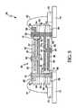
- FIG. 3illustrates another embodiment of coil transducer 39 of the invention
- FIG. 4shows comparative S-parameter modeling data for coil transducers isolators having different thicknesses of shielding
- FIG. 5illustrates one embodiment of coil transducer 39 and galvanic isolator 20 of the invention
- FIG. 6illustrates another embodiment of galvanic isolator 20 and coil transducers 39 a - 39 e of the invention
- FIGS. 7( a ) and 7 ( b )illustrate yet another embodiment of galvanic isolator 20 and coil transducer 39 of the invention.
- horizontalas used herein is defined as a plane substantially parallel to the conventional plane or surface of the substrate of the invention, regardless of its actual orientation in space.
- verticalrefers to a direction substantially perpendicular to the horizontal as defined above. Terms such as “on,”, “above,” “below,” “bottom,” “top,” “side,” “sidewall,” “higher,” “lower,” “upper,” “over” and “under” are defined in respect of the horizontal plane discussed above.
- FIGS. 1 and 2there is shown one embodiment of coil transducer 39 of the invention.
- FIG. 1shows a top plan view of coil transducer 39
- FIG. 2shows a cross-sectional view of coil transducer 39 along line 2 - 2 of FIG. 1 .
- Coil transducer 39is configured to send data and/or power signals from a transmitter circuit 21 to a receiver circuit 22 (not shown in FIGS. 1 and 2 ) across a dielectric barrier.
- a dielectric barriercomprises substrate 33 , which is disposed between an input or first transmitting coil 23 and an output or second receiving coil 24 .
- Coil transducer 39 and substrate 33 disposed therewithinmay comprise any of a number of different non-metallic, non-semiconductor, low dielectric loss materials and/or layers, more about which is said below.
- coil transducer 39 and substrate 33are capable of withstanding several kilovolts of potential difference between the input and output sides of coil transducer 39 , and thus exhibit high voltage breakdown performance characteristics.
- substrate 33 and coil transducer 39have sufficient thicknesses between upper and lower horizontal surfaces thereof, and electrical insulation characteristics appropriate, to withstand the relatively high breakdown voltages.
- a breakdown voltage between coil 23 and coil 24exceeds about 2,000 volts RMS when applied over a time period of about one minute. In other embodiments, the breakdown voltage between coil 23 and coil 24 exceeds about 2,000 volts RMS when applied over six minutes or over 24 hours.
- even higher breakdown voltagescan be withstood by coil transducer 39 , substrate 33 and galvanic isolator 20 , such as about 2,500 volts RMS, about 3,000 volts RMS, about 4,000 volts RMS and about 5,000 volts RMS for periods of time of about 1 minute, 6 minutes and/or 24 hour, or over the design lifetime of the device.
- Substrate 33 and/or coil transducer 39are formed of one or more appropriate electrically insulating, non-metallic, non-semiconductor, low dielectric loss materials.
- a suitable materialhas a dielectric loss tangent at room temperature that is less than about 0.05, less than about 0.01, less than about 0.001 or less than about 0.0001. Further information regarding dielectric loss tangents and the intrinsic and extrinsic losses associated therewith is set forth in “Loss Characteristics of Silicon Substrate with Different Resistivities” to Yang et al., pp. 1773-76, vol. 48, No. 9, September 2006, Microwave and Optical Technology Letters. Yang et al. discuss theoretically and experimentally dividing dielectric losses into an intrinsic loss tangent of silicon and an extrinsic loss associated with substrate leakage losses, and demonstrate that as doping levels in silicon increase, extrinsic losses also increase.
- suitable materials for forming substrate 33 and/or various layers included in coil transducer 39also include, but are not limited to, one or more of printed circuit board material, FR4 and other printed circuit board materials, fiberglass, glass, ceramic, polyimide, polyimide film, a polymer, an organic material, a combination of an organic filler such as epoxy and an inorganic solid such as glass, a flex circuit material, epoxy, epoxy resin, a printed circuit board material, plastic, DUPONTTM KAPTONTM, DUPONTTM PYRALUX ABTM laminate, and a ROGERSTM material (e.g., PTFE—or polytetrafluoroethylene—and glass, PTFE and ceramic, PTFE, glass and ceramic, or thermoset plastic).
- a ROGERSTM materiale.g., PTFE—or polytetrafluoroethylene—and glass, PTFE and ceramic, PTFE, glass and ceramic, or thermoset plastic.
- substrate 33is formed from material from which substrate 33 is formed.
- material from which substrate 33 is formedwill, in general, depend on cost, the degree or amount of electrical isolation or voltage breakdown protection that is desired, the particular application at hand, and other factors or considerations.
- glass and ceramic substratesare well suited for applications involving high voltages; to reduce manufacturing and processing costs, flex circuit substrates may be employed.
- substrate 33 and/or coil transducer 39has a thickness between the upper and lower horizontal surfaces thereof ranging between about 0.5 mils and about 25 mils. In one embodiment, the thickness of substrate 33 and/or coil transducer 39 exceeds about 1.5 mils. In another embodiment, substrate 33 and/or coil transducer 39 comprises a plurality of layers, where at least one of the layers comprises a low dielectric loss material.
- the structures illustrated in FIGS. 1 and 2may be fabricated using a conventional printed circuit board fabrication line.
- the cost of manufacturing coil transducer 39may be much less than that of a coil transducer constructed from silicon on a semiconductor fabrication line.
- Embodiments of coil transducer 39 based on flexible organic/inorganic or organic substratesare particularly attractive.
- Printed circuit boards or circuit carriersare known in the art, and hence need not be discussed in detail here. It is worth noting, however, that substrates 33 and coil transducers 39 of the invention that are formed from printed circuit board materials do provide an excellent low-cost alternative to silicon-based fabrication methods and materials.
- Printed circuit board materialsare less expensive, easier to handle, and more amenable to quick design or manufacturing changes than silicon-based materials.
- printed circuit boardsmay be fabricated by depositing a thin metal layer, or attaching a thin metal layer, on a somewhat flexible organic/inorganic substrate formed of fiberglass impregnated with epoxy resin and then converting the layer into a plurality of individual conductors using conventional photolithographic techniques. Additional metal layers may be added atop the thin metal layer after an intervening electrically insulating layer or coating has been laid down on the thin metal layer.
- Flex circuit technologymay also be employed to form substrate 33 and/or coil transducer 39 of galvanic isolator 20 , where substrate 33 and/or coil transducer 39 are made of an organic material such as polyimide. Films and laminates of this type are available commercially from DUPONTTM and utilize substrate materials known as KAPTONTM made from polyimide. In some cases, a plurality of polyimide layers may be laminated with an adhesive to form substrate 33 and/or coil transducer 39 .
- This type of circuit carrier or printed circuit boardis significantly less expensive than conventional silicon semiconductor material based approaches and can be employed to provide substrate 33 and/or coil transducer 39 having a high breakdown voltage and other desirable high voltage isolation characteristics.
- Thinner substrates 33 and/or coil transducers 39are preferred in applications where signal losses between primary and secondary coils 23 and 24 must be minimized.
- a PYRALUX APTM laminate manufactured by DUPONTTMis employed to form a 2 mil thick KAPTONTM substrate 33 , and electrically conductive copper layers and traces are added to the top and bottom surfaces thereof.
- coils 23 and 24may assume any of a number of different structural configurations and nevertheless fall within the scope of the invention.
- coils 23 and 24may assume the circular or oval spirally-wound shapes illustrated in FIGS. 1 and 2 , or may assume myriad other shapes such as rectangularly, squarely, triangularly, pentagonally, hexagonally, heptagonally or octagonally-wound shapes arranged in a horizontal plane, conductors arranged to interleave with one another within a horizontal plane, one or more serpentine conductors arranged in a horizontal plane, and so on. Any suitable structural configuration of coils 23 and 24 is permitted so long as the magnetic fields projected by one coil may be received and sufficiently well detected by the other opposing coil.
- substrate 33 and/or coil transducer 39are preferably fabricated to have a thickness between their respective upper and lower surfaces sufficient to prevent high voltage arcing.
- One advantage of the materials employed to form substrate 33 and/or coil transducer 39 of the inventionis that substrate 33 and/or coil transducer 39 may be substantially thicker than is generally possible or financially feasible in commercial applications which employ conventional semiconductor materials and manufacturing processes.
- substrate 33 and/or coil transducer 39may have thicknesses ranging between about 1 mil and about 25 mils, between about 1.5 mils and about 25 mils, or between about 2 mils and about 25 mils.
- DTIdistance-through-insulation
- substrate 33 and/or coil transducer 39 of the inventionmay be formed using any of a number of different manufacturing processes and electrically insulating, non-metallic, non-semiconductor, low dielectric loss materials described above. These processes and materials are amenable to processing bulk electrically insulating materials and do not require the expensive and elaborate procedures required to handle semiconductor materials such as silicon. Moreover, substrate 33 and coil transducer 39 of the invention provide superior high voltage breakdown performance characteristics respecting silicon-based devices owing to their increased distances-through-insulation (more about which is said above).
- substrate 33 and coil transducer 39 of the inventionexhibit substantially increased distances-though-insulation and thicknesses respecting prior art galvanic isolators having silicon substrates (which were generally limited to distances-through-insulation thicknesses of less than 1 mil)
- substrate 33may be configured to impart substantial mechanical rigidity and strength to coil transducer 39 and galvanic isolator 20 such that coil transducer 39 may be handled during normal manufacturing processes without the conductors disposed on, in or near substrate 33 breaking or fracturing.
- substrate 33 and coil transducer 39 of the inventionare mechanically robust and strong, may be mounted directly on lead frames, and may be handled without special care.
- substrates or coil transducers formed from semiconductor materialsare typically handled in a manner that requires metalized or other layers be formed on one side only of such substrates.
- both sides of substrate 33 and/or coil transducer 39may easily have coils or other components formed or mounted thereon owing to the radically different nature of the manufacturing processes used, and the materials employed, to form substrate 33 and/or coil transducer 39 .
- substrate 33separates coils 23 and 24 , and forms a portion of coil transducer 39 , which comprises electrically insulating layers 32 , 34 , 37 and 38 .
- layers 34 and 37are formed of an electrically insulating, non-metallic, non-semiconductor, low dielectric loss material described in greater detail below, while layers 32 and 38 are formed of an electrically insulating coating or coverlay material, more about which is also said below.
- Other embodiments of layers 32 , 34 , 37 and 38are also possible.
- coil transducer 39comprises first coil 23 and second coil 24 .
- First and second coils 23 and 24are separated from one another by an electrically insulating, non-metallic, non-semiconductor, low dielectric loss material forming substrate 33 disposed therebetween, which is a dielectric barrier.
- Upper and lower surfaces of substrate 33 , and layers 32 , 34 , 37 and 38are delineated in the Figures by dashed lines.
- the same or similar material employed to form substrate 33may be used to form dielectric or electrically insulating layers 34 and 37 disposed above and below substrate 33 , and in which electrical conductors 23 , 27 , 24 and 28 may be embedded or otherwise formed. Alternatively, other suitable materials may be employed to form such layers.
- such electrical conductorsare spirally or ovally shaped, although many other configurations and shapes for such conductors may be employed.
- coils 23 and 24may be placed on, in or near substrate 33 , or on, in, near or under layers 34 or 37 . Many other variations and embodiments are also possible.
- substrate 33 and coil transducer 39can also be configured to impart substantial structural rigidity and strength to galvanic isolator 20 , and thereby eliminate the need to include an independent structural member that is separate and apart from a coil transducer, and that is required to impart structural rigidity and strength thereto, such as has been practiced in the prior art by way of, for example, providing a thick (e.g., 25-100 mils) silicon substrate beneath a coil transducer or galvanic isolator.
- the outer otherwise exposed metalized layers of coil transducer 39are preferably protected by an electrically insulating or dielectric coating or coverlay layers 32 and 38 .
- coating or coverlay layers 32 and 38are relatively thin and conform to the pattern of etched metal spiral conductors 27 and 28 disposed therebeneath.
- Coating or coverlay layers 32 and 38should have few or no empty regions or voids disposed therebeneath or therein so as to prevent high voltage breakdown thereacross owing to the reduced ability of the empty region or void to withstand high voltages compared to, for example, polyimide.
- a vacuummay be drawn while laminating the different layers of coil transducer 39 together, or by degassing liquid photo-imageable coverlay materials before they are applied. Since an electrically insulating, non-metallic, non-semiconductor, low dielectric loss material such as polyimide disposed beneath the coating or coverlay material may be relatively thin, the ability to withstand high voltages may not be as good through coating or coverlay layers 32 and 38 as through substrate 33 (regardless of whether or not voids are present in or adjacent to coating or coverlay layers 32 and 38 ).
- first coil 23comprises a first spiral electrical conductor 23 and a second spiral electrical conductor 27 .
- Second spiral conductor 27is located above first spiral conductor 23 and is disposed in a second metalized layer, while first spiral conductor 23 is located below second spiral conductor 27 and is disposed in a first metalized layer.
- First and second spiral conductors 23 and 27are electrically connected to one another by vertical metal via 35 , which electrically interconnects the first and second metalized layers and first and second spiral conductors 23 and 27 disposed therein.
- the first and second metalized layers, and first and second spiral conductors 23 and 27are configured and positioned respecting one another such that electrical current rotates in the same direction through first and second spiral conductors 23 and 27 . Maintaining the same sense of rotation causes the magnetic fields generated by first and second spiral conductors 23 and 27 to add constructively to one another instead of cancelling one another.
- second coil 24comprises third spiral electrical conductor 24 and fourth spiral electrical conductor 28 .
- Third spiral conductor 24is located above fourth spiral conductor 28 and is disposed in a third metalized layer, while fourth spiral conductor 28 is located below third spiral conductor 24 and is disposed in a fourth metalized layer.
- Third and fourth spiral conductors 24 and 28are electrically connected to one another by vertical metal via 31 , which electrically interconnects the third and fourth metalized layers and spiral conductors 24 and 28 disposed therein.
- the third and fourth metalized layers, and third and fourth spiral conductors 24 and 28are configured and positioned respecting one another such that electrical current rotates in the same direction through third and fourth spiral conductors 24 and 28 . Maintaining the same sense of rotation causes the magnetic fields generated by third and fourth spiral conductors 24 and 28 to add constructively to one another instead of cancelling one another.
- regions 11 and 12 in coil transducer 39represent those portions of coil transducer 39 where internal high voltage breakdown may be most likely to occur. This is due to distance D 1 between spiral conductors 24 and 28 (which are held at a first voltage) and vertical metal via 36 (which is held a second voltage different from the first voltage) being relatively small. Furthermore, voids or adhesives which may be present in this region do not withstand as high voltages per unit distance as solid insulators such as KAPTON.TM By way of example, in some embodiments of the invention distance D 1 may range between about 2 mils and about 10 mils.
- first spiral conductor 23 and third spiral conductor 24are closer to first spiral conductor 23 and third spiral conductor 24 , where distance D 2 between first spiral conductor 23 (which is held at a first voltage) and third spiral conductor 24 (which is held at a second voltage different from the first voltage) can be relatively large.
- the gaps shown in FIG. 2 between vertical vias 30 and 36 on the one hand, and conductors 27 , 23 , 24 and 28 on the other handneed not be all be restricted to the same distance D 1 , and indeed may assume any of a number different suitable values.
- distance D 1is greater than or equal to distance D 2 , since high voltage breakdowns may occur at horizontally opposed internal interfaces more easily than through vertically opposed internal interfaces (where bulk material must generally be traversed to effect a voltage breakdown) owing to the lower critical electric field potentials typically associated with horizontally opposed interfaces, voids or adhesives.
- distance D 2corresponds to the distance or separation between the lower surface of first spiral conductor 23 and the upper surface of third spiral conductor 24 , and also corresponds to a distance extending vertically across substrate 33 forming the dielectric barrier and comprising the special non-metallic, non-semiconductor, low dielectric loss materials discussed above. That is, in the embodiment shown in FIG. 2 , distance D 2 corresponds to the thickness of substrate 33 and in some preferred embodiments exceeds about 0.5 mils, about 1 mil, about 2 mils, about 3, mils, about 4 mils, about 5 mils, about 6 mils, about 7 mils, about 8 mils, about 9 mils and about 10 mils.
- wirebond pads 59 , 60 , 62 and 63are located on the top surface of coil transducer 39 .
- access to the third and fourth metalized layersmust somehow be provided from the top surface of coil transducer 39 , such as by disposing conductive via 30 between such layers and wirebond contact 59 .
- Wirebond pads 59 , 60 , 62 and 63are preferably electroplated to facilitate the establishment of electrical connections.
- Holescan be formed in the top coating or coverlay material to permit access to wirebond pads 59 , 60 , 62 and 63 .
- two via holescan be formed that extend from locations 52 and 53 disposed atop coil transducer 39 down to the third and fourth metalized layers, respectively (and which contain third and fourth spiral conductors 24 and 28 ).
- Conductive via 31can be configured to route a signal between the fourth metalized layer and the third metalized layer, and wirebond pads 59 and 63 can be electroplated to permit the third and fourth metalized layers to be accessed electrically therethrough.
- the embodiment illustrated in FIGS. 1 and 2offers the convenience of easy topside wirebonding access to each of the first, second, third and fourth metalized layers.
- FIGS. 1 and 2also features an increased risk of internal high voltage breakdown between such full through vias and coils 23 and 24 , especially if voids have formed between any of the various layers of coil transducer 39 during manufacturing, more about is said below.
- FIG. 3there is shown a cross-sectional view of another embodiment of coil transducer 39 of the invention, where portions of vertical via 36 extending downwardly beyond the first metalized layer, and portions of vertical via 30 extending upwardly beyond the third metalized layer, have been eliminated therefrom.
- Such a configurationeliminates the potential high voltage breakdown problems arising from the horizontal proximities of via 36 to the third and fourth metalized layers, and via 30 to the second and first metalized layers (as shown in FIG. 2 and denoted by distances D 1 ).
- the embodiment illustrated in FIG. 3features distance D 2 as the closet dimension between the various components of coil 23 on the one hand, and coil 24 on the other hand, which as described above are often at very different electrical potentials respecting one another.
- FIG. 3provides improved performance compared to the embodiment shown in FIG. 2 .
- the embodiment illustrated in FIG. 3also eliminates major portions of vertical vias 30 and 36 in respect of the embodiment shown in FIG. 2 .
- coating or coverlay material 32 and 38is disposed over otherwise exposed coils 23 and 24 .
- electrical connections to transmitter circuit 21 and receiver circuit 22(not shown in FIG. 3 ) are established through wirebond pads 60 and 62 (see, for example, FIG. 1 ), and through wirebond pads 61 and an additional wirebond pad (not shown in FIG. 3 ), and which are located on opposing respective top and bottom sides of coil transducer 39 .
- wirebond pads 60 and 62see, for example, FIG. 1
- wirebond pads 61 and an additional wirebond padnot shown in FIG. 3
- conductive vias 36 and 30need only penetrate two metalized layers so that, for example, electrical signals need only be routed from wirebond pad 62 to spiral conductor 27 , then through via 35 to coil 23 , and then up through via 36 to wirebond pad 60 .
- electrical signalsneed only be routed between the third and fourth metalized layers and then to wirebond pad 61 .
- metal landing pads 51 , 54 , 57 and 58can be made smaller.
- vias 36 and 30do not consume as much real estate or volume in coil transducer 39 of FIG. 3 as in the embodiments illustrated in FIGS. 1 and 2 , which in turn permits coil transducer 39 to be made smaller.
- internal high voltage breakdown performanceis improved in the embodiment shown in FIG. 3 respecting the embodiment of FIGS. 1 and 2 .
- the embodiment of FIG. 3must be turned over to complete wirebonding, while all wirebonding can be carried out in the embodiment of FIGS. 1 and 2 without turning over coil transducer 39 .
- a metal shield planecan help reduce undesired outside electromagnetic interference from interfering with the operation of coil transducer 39 or galvanic isolator 20 . If such a metal shield plane is located too close to coils 23 or 24 , however, the metal shield plane may attenuate the magnetic fields generated by coil transducer 39 .
- FIG. 5shows electromagnetic modeling results generated using software from Computer Simulation TechnologyTM (“CST”) for a galvanic isolator having a metal shield plane located about 10 mils from a coil transducer (circles), about 100 mils from a coil transducer (triangles), and with no metal shield (upside-down triangles). As shown in FIG.
- CSTComputer Simulation TechnologyTM
- S 21 signal through-parameter performancedegrades substantially when a metal shield plane is brought too close to a coil transducer (e.g., a separation of only 10 mils).
- a metal shield planeis brought too close to a coil transducer (e.g., a separation of only 10 mils).
- Related modeling workindicates that a 50 mil thickness of silicone or other suitable electrically insulating material or molding compound may also function as an effective shield, even when no metal is disposed therein. Because high throughput is desired for both signal and power applications, locating any metal—even a metal shield plane held at approximately the same potential as nearby coils 23 or 24 —over or near such coils at a separation distance of 50 mils or less may degrade throughput performance top an unacceptable degree.
- coil 23 and coil 24 of coil transducer 39are located directly over (in respect of a vertical direction) a metal lead frame, which is typically at a very different potential.
- a metal lead framewhich is typically at a very different potential.
- transmitter circuit 21might be running at a potential 5 kV different from receiver circuit 22 .
- an input lead frame for galvanic isolator 20which is at a similar potential to coil 23 should not extend directly beneath coil 24 .
- galvanic isolator 20is preferably configured such that input lead frame 71 extends beneath input wirebond pads to facilitate wirebonding and provide firm structural support thereunder, but terminates before extending directly beneath coil 24 .
- output lead frame 73preferably extends beneath output wirebond pads to facilitate wirebonding and provide firm structural support thereunder, but terminates before extending directly beneath either via 30 or the via under 53 .
- FIG. 5A cross-sectional view of one embodiment of galvanic isolator 20 satisfying such design criteria is shown in FIG. 5 . In the embodiment shown in FIG.
- wirebond pads 59 and 60are located on the top surface of coil transducer 39 , and are operably connected to transmitter IC 21 through wirebonds 41 , and receiver IC 22 through wirebonds 42 , respectively.
- access to the third and fourth metalized layersis provided from the top surface of coil transducer 39 by conductive vias 30 . 36 and a via disposed beneath location 53 (see FIG. 1 ).
- FIG. 6A top view of another embodiment of galvanic isolator 20 comprising a plurality of coil transducers 39 a - 39 e satisfying the design criteria discussed hereinabove is shown in FIG. 6 .
- busbarsshould be located so that a bias voltage may be provided to wirebond pads during electroplating, thereby to facilitate the establishment of reliable wirebonded connections.
- the busbarsmust reach to the edges of coil transducer 39 so that a bias voltage may be applied during an electroplating process.
- a first busbaris operably connected to first coil 23
- a second busbaris operably connected to second coil 24 . If a busbar end is located directly over a lead frame operating at a significantly different electrical potential than the busbar, an external high voltage breakdown can occur along the edge of coil transducer 39 between the end of the busbar and the lead frame.
- Busbars and busbar endsare therefore preferably spaced far enough apart that external high voltage breakdowns cannot occur between them, and not directly above or below a lead frame at a significantly different potential.
- a first busbar for coil 23is located relatively close to an input lead frame, while a second busbar for coil 24 is located relatively close to an output lead frame.
- busbars or portions of busbarsare separated from one another, as well as from lead frames, by at least about 75 mils.
- FIGS. 7( a ) and 7 ( b )there is shown an embodiment of galvanic isolator 20 where wirebond connections to the input and output sides of coil transducer 39 are disposed on opposing sides thereof.
- FIGS. 7( a ) and 7 ( b )show cross-sectional views of galvanic isolator 20 in different stages of package assembly.
- transmitter circuit 21is attached to input lead frame 71 by, for example, electrically non-conductive epoxy, and then operably connected to the input side of coil transducer 39 through wirebond 41 and wirebond pad 60 .
- isolator 20is flipped over and receiver circuit 22 is attached to output lead frame 73 by, for example, electrically non-conductive epoxy, and then operably connected to the output side of coil transducer 39 through wirebond 42 and wirebond pad 61 (see FIG. 7( b )).
- the configuration of galvanic isolator 20 shown in FIGS. 7( a ) and 7 ( b )eliminates the potential high voltage breakdown problems arising from the horizontal proximities of via 36 to the third and fourth metalized layers, and of via 30 to the second and first metalized layers shown in FIG. 2 and denoted by distances D 1 .
- galvanic isolator 20 of FIGS. 7( a ) and 7 ( b )features input lead frame 71 and output lead frame 73 positioned in respect of galvanic isolator 20 such that structural support is provided thereto by lead frames 71 and 73 . This reduces the probability or possibility of external arcing because lead frames 71 and 73 do not extend beneath isolator 20 or coil transducer 39 sufficiently far so as to be located directly beneath coils 23 or 24 .
- isolator 20is preferably potted in a dielectric potting material that inhibits or prevents the occurrence of external high voltage breakdown (not shown in the Figures).
- This dielectric materialshould wet or adhere to the surfaces of coil transducer 39 , lead frames 71 and 73 , and ICs 21 and 22 such that no or few voids form or are included in the potting material after it has cured or dried.
- the dielectric potting materialpreferably exhibits high voltage hold-off and low dielectric loss performance characteristics so that the magnetic fields generated by isolator 20 are not attenuated.
- the dielectric potting materialshould also have a coefficient of thermal expansion similar to that of coil transducer 39 so that excessive stress is not placed on layers disposed within coil transducer 39 ; otherwise, spiral conductors 23 , 27 , 24 or 28 may break or fracture.
- a first dielectric potting materialmay be placed around various or all portions of isolator 20 , followed by placing a second dielectric potting material around the first dielectric potting material, the second dielectric potting material forming an external surface of isolator 20 .
- suitable dielectric potting materialsinclude silicone, electrically non-conductive epoxy, polyimide, glass-filled epoxy and glass- and carbon-filled epoxy.
- galvanic isolator 20is overmolded.
- lead frame 71 with transmitter integrated circuit 21 , and coil transducer 39 attached thereto, and lead frame 73 with receiver integrated circuit 22 and coil transducer 39 attached theretoare wirebonded, placed in a mold, and a melted appropriate electrically insulating molding material such as glass-filled epoxy is forced into the mold to encapsulate at least portions of the package.
- the molding materialis then allowed to cool and harden, thereby providing electrical insulation and imparting substantial additional structural rigidity to the resulting package.
- the molding materialpreferably has an appropriate dielectric constant and low dielectric loss such that the electrical performance of galvanic isolator 20 is not degraded.
- the leadsare then trimmed and bent.
- any one or more of the first, second, third, and fourth metalized layers, and vias 30 , 31 , 35 and 36may be formed of one or more of gold, silver, copper, tungsten, nickel, tin, aluminum, aluminum-copper, and alloys, combinations or mixtures thereof.
- coil transducer 39may be mounted on a printed circuit board or a flex circuit substrate instead of being mounted on one or more lead frames.
- packaging examples described and shown hereinare not meant to cover all possibilities for packaging coil transducer 39 of the invention, and many different variations and permutations are contemplated.
Landscapes
- Engineering & Computer Science (AREA)
- Power Engineering (AREA)
- Multimedia (AREA)
- Coils Or Transformers For Communication (AREA)
Abstract
Description
Claims (31)
Priority Applications (7)
| Application Number | Priority Date | Filing Date | Title |
|---|---|---|---|
| US12/059,747US7852186B2 (en) | 2006-08-28 | 2008-03-31 | Coil transducer with reduced arcing and improved high voltage breakdown performance characteristics |
| US12/370,208US9105391B2 (en) | 2006-08-28 | 2009-02-12 | High voltage hold-off coil transducer |
| US12/393,596US8061017B2 (en) | 2006-08-28 | 2009-02-26 | Methods of making coil transducers |
| US12/477,078US8385043B2 (en) | 2006-08-28 | 2009-06-02 | Galvanic isolator |
| US12/752,019US8427844B2 (en) | 2006-08-28 | 2010-03-31 | Widebody coil isolators |
| US12/751,971US8093983B2 (en) | 2006-08-28 | 2010-03-31 | Narrowbody coil isolator |
| US12/957,446US8258911B2 (en) | 2008-03-31 | 2010-12-01 | Compact power transformer components, devices, systems and methods |
Applications Claiming Priority (3)
| Application Number | Priority Date | Filing Date | Title |
|---|---|---|---|
| US11/512,034US7791900B2 (en) | 2006-08-28 | 2006-08-28 | Galvanic isolator |
| US11/747,092US20080278275A1 (en) | 2007-05-10 | 2007-05-10 | Miniature Transformers Adapted for use in Galvanic Isolators and the Like |
| US12/059,747US7852186B2 (en) | 2006-08-28 | 2008-03-31 | Coil transducer with reduced arcing and improved high voltage breakdown performance characteristics |
Related Parent Applications (4)
| Application Number | Title | Priority Date | Filing Date |
|---|---|---|---|
| US11/512,034Continuation-In-PartUS7791900B2 (en) | 2006-08-28 | 2006-08-28 | Galvanic isolator |
| US11/747,092Continuation-In-PartUS20080278275A1 (en) | 2006-08-28 | 2007-05-10 | Miniature Transformers Adapted for use in Galvanic Isolators and the Like |
| US12/059,979Continuation-In-PartUS9019057B2 (en) | 2006-08-28 | 2008-03-31 | Galvanic isolators and coil transducers |
| US12/370,208Continuation-In-PartUS9105391B2 (en) | 2006-08-28 | 2009-02-12 | High voltage hold-off coil transducer |
Related Child Applications (4)
| Application Number | Title | Priority Date | Filing Date |
|---|---|---|---|
| US11/512,034Continuation-In-PartUS7791900B2 (en) | 2006-08-28 | 2006-08-28 | Galvanic isolator |
| US12/059,979Continuation-In-PartUS9019057B2 (en) | 2006-08-28 | 2008-03-31 | Galvanic isolators and coil transducers |
| US12/392,978Continuation-In-PartUS7741943B2 (en) | 2006-08-28 | 2009-02-25 | Miniature transformers adapted for use in galvanic isolators and the like |
| US12/957,446Continuation-In-PartUS8258911B2 (en) | 2008-03-31 | 2010-12-01 | Compact power transformer components, devices, systems and methods |
Publications (2)
| Publication Number | Publication Date |
|---|---|
| US20080180206A1 US20080180206A1 (en) | 2008-07-31 |
| US7852186B2true US7852186B2 (en) | 2010-12-14 |
Family
ID=39667288
Family Applications (1)
| Application Number | Title | Priority Date | Filing Date |
|---|---|---|---|
| US12/059,747Expired - Fee RelatedUS7852186B2 (en) | 2006-08-28 | 2008-03-31 | Coil transducer with reduced arcing and improved high voltage breakdown performance characteristics |
Country Status (1)
| Country | Link |
|---|---|
| US (1) | US7852186B2 (en) |
Cited By (20)
| Publication number | Priority date | Publication date | Assignee | Title |
|---|---|---|---|---|
| US20080278256A1 (en)* | 2007-05-11 | 2008-11-13 | Intersil Americas Inc. | Rf - coupled digital isolator |
| US20110206328A1 (en)* | 2010-02-25 | 2011-08-25 | Emcore Corporation | Optoelectronic module with emi shield |
| US8093983B2 (en)* | 2006-08-28 | 2012-01-10 | Avago Technologies Ecbu Ip (Singapore) Pte. Ltd. | Narrowbody coil isolator |
| US20120098349A1 (en)* | 2010-10-20 | 2012-04-26 | Electronics And Telecommunications Research Institute | Wireless power transfer device |
| US20120146757A1 (en)* | 2010-12-08 | 2012-06-14 | Industrial Technology Research Institute | Three dimensional inductor |
| DE102011081268A1 (en) | 2011-08-19 | 2013-02-21 | Endress + Hauser Gmbh + Co. Kg | Field device for determining or monitoring a physical or chemical process variable in automation technology |
| CN104104348A (en)* | 2014-08-01 | 2014-10-15 | 王少夫 | Adjustable printing plate transformer |
| US9029818B2 (en) | 2012-06-21 | 2015-05-12 | Avago Technologies General Ip (Singapore) Pte. Ltd. | Optoelectronic device and method of manufacture |
| US20150357113A1 (en)* | 2013-01-22 | 2015-12-10 | Phoenix Contact Gmbh & Co.Kg | Printed circuit board having a layer structure |
| US9508485B1 (en)* | 2012-10-04 | 2016-11-29 | Vlt, Inc. | Isolator with integral transformer |
| US20170062119A1 (en)* | 2015-08-24 | 2017-03-02 | Qorvo Us, Inc. | Stacked laminate inductors for high module volume utilization and performance-cost-size-processing-time tradeoff |
| US9761553B2 (en)* | 2012-10-19 | 2017-09-12 | Taiwan Semiconductor Manufacturing Company Limited | Inductor with conductive trace |
| US10320339B2 (en) | 2013-03-15 | 2019-06-11 | Qirvo US, Inc. | Weakly coupled based harmonic rejection filter for feedback linearization power amplifier |
| US10468172B2 (en) | 2013-03-15 | 2019-11-05 | Qorvo Us, Inc. | Advanced 3D inductor structures with confined magnetic field |
| US10923417B2 (en) | 2017-04-26 | 2021-02-16 | Taiwan Semiconductor Manufacturing Company Limited | Integrated fan-out package with 3D magnetic core inductor |
| US10965258B2 (en) | 2013-08-01 | 2021-03-30 | Qorvo Us, Inc. | Weakly coupled tunable RF receiver architecture |
| US11139238B2 (en) | 2016-12-07 | 2021-10-05 | Qorvo Us, Inc. | High Q factor inductor structure |
| US11189563B2 (en)* | 2019-08-01 | 2021-11-30 | Nanya Technology Corporation | Semiconductor structure and manufacturing method thereof |
| US12224096B2 (en) | 2013-03-15 | 2025-02-11 | Qorvo Us, Inc. | Advanced 3D inductor structures with confined magnetic field |
| USRE50365E1 (en) | 2015-01-14 | 2025-04-08 | Vicor Corporation | Power adapter packaging |
Families Citing this family (27)
| Publication number | Priority date | Publication date | Assignee | Title |
|---|---|---|---|---|
| US8427844B2 (en)* | 2006-08-28 | 2013-04-23 | Avago Technologies Ecbu Ip (Singapore) Pte. Ltd. | Widebody coil isolators |
| US9019057B2 (en)* | 2006-08-28 | 2015-04-28 | Avago Technologies General Ip (Singapore) Pte. Ltd. | Galvanic isolators and coil transducers |
| US8061017B2 (en)* | 2006-08-28 | 2011-11-22 | Avago Technologies Ecbu Ip (Singapore) Pte. Ltd. | Methods of making coil transducers |
| US7791900B2 (en)* | 2006-08-28 | 2010-09-07 | Avago Technologies General Ip (Singapore) Pte. Ltd. | Galvanic isolator |
| US20080278275A1 (en)* | 2007-05-10 | 2008-11-13 | Fouquet Julie E | Miniature Transformers Adapted for use in Galvanic Isolators and the Like |
| US7948067B2 (en)* | 2009-06-30 | 2011-05-24 | Avago Technologies Ecbu Ip (Singapore) Pte. Ltd. | Coil transducer isolator packages |
| US9105391B2 (en) | 2006-08-28 | 2015-08-11 | Avago Technologies General Ip (Singapore) Pte. Ltd. | High voltage hold-off coil transducer |
| US8385043B2 (en)* | 2006-08-28 | 2013-02-26 | Avago Technologies ECBU IP (Singapoare) Pte. Ltd. | Galvanic isolator |
| US8258911B2 (en)* | 2008-03-31 | 2012-09-04 | Avago Technologies ECBU IP (Singapor) Pte. Ltd. | Compact power transformer components, devices, systems and methods |
| US20100077860A1 (en)* | 2008-09-30 | 2010-04-01 | Honeywell International Inc. | Systems and methods for integrated isolator and transducer components in an inertial sensor |
| US8380146B2 (en)* | 2009-12-31 | 2013-02-19 | Avago Technologies Wireless Ip (Singapore) Pte. Ltd. | Multi-band, multi-mode RF transmit amplifier system with separate signal paths for linear and saturated operation |
| US8339231B1 (en)* | 2010-03-22 | 2012-12-25 | Flextronics Ap, Llc | Leadframe based magnetics package |
| US8519815B1 (en)* | 2010-12-07 | 2013-08-27 | Tivo Inc. | Multi-layered circuit structure |
| US8421575B1 (en) | 2010-12-07 | 2013-04-16 | Tivo Inc. | Multi-layered circuit structure |
| US8614616B2 (en) | 2011-01-18 | 2013-12-24 | Infineon Technologies Ag | Semiconductor device and method of manufacture thereof |
| JP5782919B2 (en)* | 2011-08-25 | 2015-09-24 | サンケン電気株式会社 | Semiconductor device |
| US8558344B2 (en) | 2011-09-06 | 2013-10-15 | Analog Devices, Inc. | Small size and fully integrated power converter with magnetics on chip |
| US8610247B2 (en)* | 2011-12-30 | 2013-12-17 | Taiwan Semiconductor Manufacturing Company, Ltd. | Structure and method for a transformer with magnetic features |
| EP2817809A1 (en)* | 2012-02-22 | 2014-12-31 | Phoenix Contact GmbH & Co. KG | Planar transmitter with a layered structure |
| US8786393B1 (en)* | 2013-02-05 | 2014-07-22 | Analog Devices, Inc. | Step up or step down micro-transformer with tight magnetic coupling |
| US9293997B2 (en) | 2013-03-14 | 2016-03-22 | Analog Devices Global | Isolated error amplifier for isolated power supplies |
| KR101892689B1 (en) | 2014-10-14 | 2018-08-28 | 삼성전기주식회사 | Chip electronic component and board having the same mounted thereon |
| KR101883046B1 (en)* | 2016-04-15 | 2018-08-24 | 삼성전기주식회사 | Coil Electronic Component |
| KR101983191B1 (en)* | 2017-07-25 | 2019-05-28 | 삼성전기주식회사 | Inductor and method for manufacturing the same |
| JP7462525B2 (en) | 2018-06-01 | 2024-04-05 | 株式会社タムラ製作所 | Electronic Components |
| GB201818876D0 (en)* | 2018-11-20 | 2019-01-02 | Sentec Ltd | Current sensor |
| US20230005652A1 (en)* | 2021-06-30 | 2023-01-05 | Texas Instruments Incorporated | Laminate Transformer with Overlapping Lead Frame |
Citations (84)
| Publication number | Priority date | Publication date | Assignee | Title |
|---|---|---|---|---|
| US4027152A (en) | 1975-11-28 | 1977-05-31 | Hewlett-Packard Company | Apparatus and method for transmitting binary-coded information |
| JPS5739598A (en) | 1980-08-21 | 1982-03-04 | Asahi Chemical Ind | Thick film fine pattern |
| US4494100A (en)* | 1982-07-12 | 1985-01-15 | Motorola, Inc. | Planar inductors |
| US4541894A (en) | 1983-05-27 | 1985-09-17 | Rhone-Poulenc Sa | Metallizable, essentially isotropic polymeric substrates well adopted for printed circuits |
| JPS6159714A (en) | 1984-08-30 | 1986-03-27 | 松下電器産業株式会社 | Composite dielectric capacitor |
| JPH03171705A (en) | 1989-11-30 | 1991-07-25 | Toshiba Corp | plane transformer |
| US5070317A (en) | 1989-01-17 | 1991-12-03 | Bhagat Jayant K | Miniature inductor for integrated circuits and devices |
| JPH0653052A (en) | 1992-07-09 | 1994-02-25 | Murata Mfg Co Ltd | Line transformer |
| US5312674A (en)* | 1992-07-31 | 1994-05-17 | Hughes Aircraft Company | Low-temperature-cofired-ceramic (LTCC) tape structures including cofired ferromagnetic elements, drop-in components and multi-layer transformer |
| US5420558A (en) | 1992-05-27 | 1995-05-30 | Fuji Electric Co., Ltd. | Thin film transformer |
| US5597979A (en) | 1995-05-12 | 1997-01-28 | Schlegel Corporation | EMI shielding having flexible condustive sheet and I/O Gasket |
| WO1997034349A1 (en) | 1996-03-14 | 1997-09-18 | The National Grid Company Plc | Switchgear device |
| US5693871A (en) | 1996-07-12 | 1997-12-02 | The United States Of America As Represented By The Administrator Of The National Aeronautics And Space Administration | Low differential pressure generator |
| US5716713A (en)* | 1994-12-16 | 1998-02-10 | Ceramic Packaging, Inc. | Stacked planar transformer |
| CN1180277A (en) | 1996-10-06 | 1998-04-29 | 张萍 | Electromagnetic interference (FMI) suppressor for high voltage isolator |
| US5754088A (en) | 1994-11-17 | 1998-05-19 | International Business Machines Corporation | Planar transformer and method of manufacture |
| US5825259A (en) | 1994-08-03 | 1998-10-20 | Madge Networks Limited | Electromagnetic interference isolator with common mode choke |
| US5952849A (en) | 1997-02-21 | 1999-09-14 | Analog Devices, Inc. | Logic isolator with high transient immunity |
| CN1237081A (en) | 1998-02-05 | 1999-12-01 | 香港城市大学 | Ironless printed circuit board type transformer |
| JP2000508116A (en) | 1995-10-31 | 2000-06-27 | ザ ウィタカー コーポレーション | RF transformer using multilayer metal polymer structure |
| DE19911133A1 (en) | 1999-03-12 | 2000-10-05 | Eckhard Mademann | Circuit isolator for signal transmission galvanically separating input circuit from output circuit, has receiver of opto-coupler arranged between reference input and collector connection of second regulatable Zener diode |
| US6167475A (en) | 1998-07-06 | 2000-12-26 | International Business Machines Corporation | Data transfer method/engine for pipelining shared memory bus accesses |
| US6175293B1 (en) | 1988-09-30 | 2001-01-16 | Kabushiki Kaisha Toshiba | Planar inductor |
| US6215377B1 (en) | 1998-05-26 | 2001-04-10 | Microsubstrates Corporation | Low cost wideband RF port structure for microwave circuit packages using coplanar waveguide and BGA I/O format |
| JP3171705B2 (en) | 1992-11-11 | 2001-06-04 | 株式会社イノアックコーポレーション | Method of manufacturing retractable headrest |
| US6255714B1 (en)* | 1999-06-22 | 2001-07-03 | Agere Systems Guardian Corporation | Integrated circuit having a micromagnetic device including a ferromagnetic core and method of manufacture therefor |
| US6307457B1 (en)* | 1997-12-17 | 2001-10-23 | U.S. Philips Corporation | Planar transformer |
| US6320532B1 (en) | 1999-05-27 | 2001-11-20 | Rosemount Inc. | Low power radar level transmitter having reduced ground loop errors |
| US6404317B1 (en) | 1990-05-31 | 2002-06-11 | Kabushiki Kaisha Toshiba | Planar magnetic element |
| US20020110013A1 (en) | 2001-01-05 | 2002-08-15 | Samsung Electronics Co., Ltd. | Coreless superthin PCB transformer and non-contact battery charger using the same |
| US6489850B2 (en) | 2001-03-16 | 2002-12-03 | International Business Machines Corporation | Crosstalk suppression in differential AC coupled multichannel IC amplifiers |
| US6501364B1 (en) | 2001-06-15 | 2002-12-31 | City University Of Hong Kong | Planar printed-circuit-board transformers with effective electromagnetic interference (EMI) shielding |
| US6525566B2 (en) | 2000-02-14 | 2003-02-25 | Analog Devices, Inc. | Isolator for transmitting logic signals across an isolation barrier |
| US6538313B1 (en)* | 2001-11-13 | 2003-03-25 | National Semiconductor Corporation | IC package with integral substrate capacitor |
| EP1309033A2 (en) | 2001-11-01 | 2003-05-07 | Motorola, Inc. | An arrangement for radiating rf signals from a radio transmitter |
| JP2003151829A (en) | 2001-11-14 | 2003-05-23 | Fdk Corp | Chip inductor |
| DE10154906A1 (en) | 2001-10-30 | 2003-05-28 | Osram Opto Semiconductors Gmbh | Optical coupler has radiation transmitter and receiver coupled together via short optical transmission path, each mounted on substrate and opposite or adjacent to each other in housing |
| US6661079B1 (en) | 2002-02-20 | 2003-12-09 | National Semiconductor Corporation | Semiconductor-based spiral capacitor |
| US20040056749A1 (en) | 2002-07-18 | 2004-03-25 | Frank Kahlmann | Integrated transformer configuration |
| GB2403072A (en) | 2003-06-12 | 2004-12-22 | Aph Trading Pte Ltd | Electrical isolator |
| WO2005001928A2 (en) | 2003-06-23 | 2005-01-06 | Intel Corporation | Capacitor-related systems for addressing package/motherboard resonance |
| US20050003199A1 (en) | 2002-12-27 | 2005-01-06 | Tdk Corporation | Resin composition, cured resin, sheet-like cured resin, laminated body, prepreg, electronic parts and multilayer boards |
| US6856226B2 (en) | 1999-11-23 | 2005-02-15 | Intel Corporation | Integrated transformer |
| US6867678B2 (en) | 2003-01-28 | 2005-03-15 | Entrust Power Co., Ltd. | Transformer structure |
| US20050057277A1 (en) | 2003-04-30 | 2005-03-17 | Analog Devices, Inc. | Signal isolators using micro-transformer |
| US6873065B2 (en) | 1997-10-23 | 2005-03-29 | Analog Devices, Inc. | Non-optical signal isolator |
| US20050077993A1 (en)* | 2003-04-24 | 2005-04-14 | Hiroshi Kanno | High-frequency circuit |
| US6888438B2 (en) | 2001-06-15 | 2005-05-03 | City University Of Hong Kong | Planar printed circuit-board transformers with effective electromagnetic interference (EMI) shielding |
| US6891461B2 (en) | 1999-11-23 | 2005-05-10 | Intel Corporation | Integrated transformer |
| JP2005513824A (en) | 2001-05-08 | 2005-05-12 | フォームファクター,インコーポレイテッド | Electromagnetic coupling interconnect system architecture |
| US20050133249A1 (en) | 2003-12-19 | 2005-06-23 | Mitsui Mining & Smelting Co., Ltd. | Printed wiring board and semiconductor device |
| US6943658B2 (en) | 1999-11-23 | 2005-09-13 | Intel Corporation | Integrated transformer |
| US6944009B2 (en) | 2003-02-11 | 2005-09-13 | Oplink Communications, Inc. | Ultra broadband capacitor assembly |
| US20050272378A1 (en) | 2004-06-03 | 2005-12-08 | Timothy Dupuis | Spread spectrum isolator |
| US20050269657A1 (en) | 2004-06-03 | 2005-12-08 | Timothy Dupuis | On chip transformer isolator |
| EP1617337A2 (en) | 2004-07-14 | 2006-01-18 | Endress + Hauser Flowtec AG | Galvanic separation by means of radio technologies |
| US20060028313A1 (en)* | 2004-07-26 | 2006-02-09 | Infineon Technologies Ag | Component arrangement with a planar transformer |
| US7064442B1 (en) | 2003-07-02 | 2006-06-20 | Analog Devices, Inc. | Integrated circuit package device |
| US20060152322A1 (en)* | 2004-12-07 | 2006-07-13 | Whittaker Ronald W | Miniature circuitry and inductive components and methods for manufacturing same |
| US20060170527A1 (en)* | 2005-02-02 | 2006-08-03 | Henning Braunisch | Integrated transformer structure and method of fabrication |
| US20060176137A1 (en)* | 2005-01-24 | 2006-08-10 | Sanyo Electric Co., Ltd. | Semiconductor apparatus |
| US20060220775A1 (en)* | 2005-03-31 | 2006-10-05 | Fujitsu Limited | Variable inductor |
| US7170807B2 (en) | 2002-04-18 | 2007-01-30 | Innovative Silicon S.A. | Data storage device and refreshing method for use with such device |
| US7171739B2 (en)* | 2002-01-23 | 2007-02-06 | Broadcom Corporation | Method of manufacturing an on-chip transformer balun |
| US20070085447A1 (en) | 2005-10-18 | 2007-04-19 | Larson John D Iii | Acoustic galvanic isolator incorporating single insulated decoupled stacked bulk acoustic resonator with acoustically-resonant electrical insulator |
| US20070085632A1 (en) | 2005-10-18 | 2007-04-19 | Larson John D Iii | Acoustic galvanic isolator |
| US20070086274A1 (en) | 2005-10-18 | 2007-04-19 | Ken Nishimura | Acoustically communicating data signals across an electrical isolation barrier |
| US20070133933A1 (en) | 2005-12-12 | 2007-06-14 | Yoon Ho G | Enhanced coplanar waveguide and optical communication module using the same |
| US20070281394A1 (en)* | 2006-04-25 | 2007-12-06 | Ngk Spark Plug Co., Ltd. | Method for manufacturing wiring board |
| US20070290784A1 (en) | 2004-06-07 | 2007-12-20 | Arild Nesse | Planar High Voltage Transformer Device |
| US20080007382A1 (en)* | 2006-07-06 | 2008-01-10 | Harris Corporation | Transformer and associated method of making |
| US20080031286A1 (en) | 2004-06-03 | 2008-02-07 | Silicon Laboratories Inc. | Multiplexed rf isolator |
| US20080051158A1 (en) | 2006-08-22 | 2008-02-28 | Texas Instruments Incorporated | Galvanic isolation integrated in a signal channel |
| US20080176362A1 (en) | 2007-01-24 | 2008-07-24 | Dipak Sengupta | Stress free package and laminate-based isolator package |
| US20080174396A1 (en)* | 2007-01-24 | 2008-07-24 | Samsung Electronics Co., Ltd. | Transformers and baluns |
| US20080198904A1 (en) | 2007-02-15 | 2008-08-21 | Kwee Chong Chang | Multi-Channel Galvanic Isolator Utilizing a Single Transmission Channel |
| US7436282B2 (en)* | 2004-12-07 | 2008-10-14 | Multi-Fineline Electronix, Inc. | Miniature circuitry and inductive components and methods for manufacturing same |
| US20080278275A1 (en) | 2007-05-10 | 2008-11-13 | Fouquet Julie E | Miniature Transformers Adapted for use in Galvanic Isolators and the Like |
| US7460604B2 (en) | 2004-06-03 | 2008-12-02 | Silicon Laboratories Inc. | RF isolator for isolating voltage sensing and gate drivers |
| US20080311862A1 (en) | 2007-05-11 | 2008-12-18 | Stmicroelectronics S.R.L. | Integrated galvanic isolator using wireless transmission |
| US20080308817A1 (en) | 2007-06-12 | 2008-12-18 | Youfa Wang | Galvanic Isolator Having Improved High Voltage Common Mode Transient Immunity |
| US20090072819A1 (en) | 2006-01-06 | 2009-03-19 | Ntn Corporation | Rotation Angle Detector and Bearing with Rotation Angle Detector |
| US20100020448A1 (en) | 2006-08-28 | 2010-01-28 | Avago Technologies Ecbu Ip (Singapore) Pte. Ltd. | Galvanic isolator |
| US20100052120A1 (en) | 2008-09-02 | 2010-03-04 | Linear Technology Corporation | Semiconductor device having a suspended isolating interconnect |
Family Cites Families (5)
| Publication number | Priority date | Publication date | Assignee | Title |
|---|---|---|---|---|
| US5825529A (en)* | 1996-06-27 | 1998-10-20 | Xerox Corporation | Gyricon display with no elastomer substrate |
| US6761001B2 (en)* | 2000-08-18 | 2004-07-13 | Lee W. Mueller | Frame shear assembly for walls |
| DE102004038306A1 (en)* | 2004-08-04 | 2006-03-30 | Siemens Ag | Method for parameterizing an electric field device and parameterizable electric field device |
| US20060095136A1 (en)* | 2004-11-03 | 2006-05-04 | Mcluen Design, Inc. | Bone fusion device |
| US7791900B2 (en)* | 2006-08-28 | 2010-09-07 | Avago Technologies General Ip (Singapore) Pte. Ltd. | Galvanic isolator |
- 2008
- 2008-03-31USUS12/059,747patent/US7852186B2/ennot_activeExpired - Fee Related
Patent Citations (90)
| Publication number | Priority date | Publication date | Assignee | Title |
|---|---|---|---|---|
| US4027152A (en) | 1975-11-28 | 1977-05-31 | Hewlett-Packard Company | Apparatus and method for transmitting binary-coded information |
| JPS5739598A (en) | 1980-08-21 | 1982-03-04 | Asahi Chemical Ind | Thick film fine pattern |
| US4494100A (en)* | 1982-07-12 | 1985-01-15 | Motorola, Inc. | Planar inductors |
| US4541894A (en) | 1983-05-27 | 1985-09-17 | Rhone-Poulenc Sa | Metallizable, essentially isotropic polymeric substrates well adopted for printed circuits |
| JPS6159714A (en) | 1984-08-30 | 1986-03-27 | 松下電器産業株式会社 | Composite dielectric capacitor |
| US6175293B1 (en) | 1988-09-30 | 2001-01-16 | Kabushiki Kaisha Toshiba | Planar inductor |
| US5070317A (en) | 1989-01-17 | 1991-12-03 | Bhagat Jayant K | Miniature inductor for integrated circuits and devices |
| JPH03171705A (en) | 1989-11-30 | 1991-07-25 | Toshiba Corp | plane transformer |
| US6404317B1 (en) | 1990-05-31 | 2002-06-11 | Kabushiki Kaisha Toshiba | Planar magnetic element |
| US5420558A (en) | 1992-05-27 | 1995-05-30 | Fuji Electric Co., Ltd. | Thin film transformer |
| JPH0653052A (en) | 1992-07-09 | 1994-02-25 | Murata Mfg Co Ltd | Line transformer |
| US5363081A (en)* | 1992-07-09 | 1994-11-08 | Murata Manufacturing Co., Ltd. | Line transformer and manufacturing process thereof |
| US5312674A (en)* | 1992-07-31 | 1994-05-17 | Hughes Aircraft Company | Low-temperature-cofired-ceramic (LTCC) tape structures including cofired ferromagnetic elements, drop-in components and multi-layer transformer |
| JP3171705B2 (en) | 1992-11-11 | 2001-06-04 | 株式会社イノアックコーポレーション | Method of manufacturing retractable headrest |
| US5825259A (en) | 1994-08-03 | 1998-10-20 | Madge Networks Limited | Electromagnetic interference isolator with common mode choke |
| US5754088A (en) | 1994-11-17 | 1998-05-19 | International Business Machines Corporation | Planar transformer and method of manufacture |
| US5716713A (en)* | 1994-12-16 | 1998-02-10 | Ceramic Packaging, Inc. | Stacked planar transformer |
| US5597979A (en) | 1995-05-12 | 1997-01-28 | Schlegel Corporation | EMI shielding having flexible condustive sheet and I/O Gasket |
| JP2000508116A (en) | 1995-10-31 | 2000-06-27 | ザ ウィタカー コーポレーション | RF transformer using multilayer metal polymer structure |
| WO1997034349A1 (en) | 1996-03-14 | 1997-09-18 | The National Grid Company Plc | Switchgear device |
| US5693871A (en) | 1996-07-12 | 1997-12-02 | The United States Of America As Represented By The Administrator Of The National Aeronautics And Space Administration | Low differential pressure generator |
| CN1180277A (en) | 1996-10-06 | 1998-04-29 | 张萍 | Electromagnetic interference (FMI) suppressor for high voltage isolator |
| US5952849A (en) | 1997-02-21 | 1999-09-14 | Analog Devices, Inc. | Logic isolator with high transient immunity |
| US6873065B2 (en) | 1997-10-23 | 2005-03-29 | Analog Devices, Inc. | Non-optical signal isolator |
| US6307457B1 (en)* | 1997-12-17 | 2001-10-23 | U.S. Philips Corporation | Planar transformer |
| CN1237081A (en) | 1998-02-05 | 1999-12-01 | 香港城市大学 | Ironless printed circuit board type transformer |
| US6215377B1 (en) | 1998-05-26 | 2001-04-10 | Microsubstrates Corporation | Low cost wideband RF port structure for microwave circuit packages using coplanar waveguide and BGA I/O format |
| US6167475A (en) | 1998-07-06 | 2000-12-26 | International Business Machines Corporation | Data transfer method/engine for pipelining shared memory bus accesses |
| DE19911133A1 (en) | 1999-03-12 | 2000-10-05 | Eckhard Mademann | Circuit isolator for signal transmission galvanically separating input circuit from output circuit, has receiver of opto-coupler arranged between reference input and collector connection of second regulatable Zener diode |
| US6320532B1 (en) | 1999-05-27 | 2001-11-20 | Rosemount Inc. | Low power radar level transmitter having reduced ground loop errors |
| US6255714B1 (en)* | 1999-06-22 | 2001-07-03 | Agere Systems Guardian Corporation | Integrated circuit having a micromagnetic device including a ferromagnetic core and method of manufacture therefor |
| US6891461B2 (en) | 1999-11-23 | 2005-05-10 | Intel Corporation | Integrated transformer |
| US6870456B2 (en) | 1999-11-23 | 2005-03-22 | Intel Corporation | Integrated transformer |
| US6943658B2 (en) | 1999-11-23 | 2005-09-13 | Intel Corporation | Integrated transformer |
| US6856226B2 (en) | 1999-11-23 | 2005-02-15 | Intel Corporation | Integrated transformer |
| US6903578B2 (en) | 2000-02-14 | 2005-06-07 | Analog Devices, Inc. | Logic isolator |
| US6525566B2 (en) | 2000-02-14 | 2003-02-25 | Analog Devices, Inc. | Isolator for transmitting logic signals across an isolation barrier |
| US6922080B2 (en) | 2000-02-14 | 2005-07-26 | Analog Devices, Inc. | Logic isolator for transmitting periodic signals across an isolation barrier |
| US20020110013A1 (en) | 2001-01-05 | 2002-08-15 | Samsung Electronics Co., Ltd. | Coreless superthin PCB transformer and non-contact battery charger using the same |
| US6489850B2 (en) | 2001-03-16 | 2002-12-03 | International Business Machines Corporation | Crosstalk suppression in differential AC coupled multichannel IC amplifiers |
| US6574091B2 (en) | 2001-03-16 | 2003-06-03 | International Business Machines Corporation | Multi-plate capacitor structure |
| JP2005513824A (en) | 2001-05-08 | 2005-05-12 | フォームファクター,インコーポレイテッド | Electromagnetic coupling interconnect system architecture |
| US6501364B1 (en) | 2001-06-15 | 2002-12-31 | City University Of Hong Kong | Planar printed-circuit-board transformers with effective electromagnetic interference (EMI) shielding |
| US6888438B2 (en) | 2001-06-15 | 2005-05-03 | City University Of Hong Kong | Planar printed circuit-board transformers with effective electromagnetic interference (EMI) shielding |
| DE10154906A1 (en) | 2001-10-30 | 2003-05-28 | Osram Opto Semiconductors Gmbh | Optical coupler has radiation transmitter and receiver coupled together via short optical transmission path, each mounted on substrate and opposite or adjacent to each other in housing |
| EP1309033A2 (en) | 2001-11-01 | 2003-05-07 | Motorola, Inc. | An arrangement for radiating rf signals from a radio transmitter |
| US6538313B1 (en)* | 2001-11-13 | 2003-03-25 | National Semiconductor Corporation | IC package with integral substrate capacitor |
| JP2003151829A (en) | 2001-11-14 | 2003-05-23 | Fdk Corp | Chip inductor |
| US7171739B2 (en)* | 2002-01-23 | 2007-02-06 | Broadcom Corporation | Method of manufacturing an on-chip transformer balun |
| US6661079B1 (en) | 2002-02-20 | 2003-12-09 | National Semiconductor Corporation | Semiconductor-based spiral capacitor |
| US7170807B2 (en) | 2002-04-18 | 2007-01-30 | Innovative Silicon S.A. | Data storage device and refreshing method for use with such device |
| US20040056749A1 (en) | 2002-07-18 | 2004-03-25 | Frank Kahlmann | Integrated transformer configuration |
| US20050003199A1 (en) | 2002-12-27 | 2005-01-06 | Tdk Corporation | Resin composition, cured resin, sheet-like cured resin, laminated body, prepreg, electronic parts and multilayer boards |
| US6867678B2 (en) | 2003-01-28 | 2005-03-15 | Entrust Power Co., Ltd. | Transformer structure |
| US6944009B2 (en) | 2003-02-11 | 2005-09-13 | Oplink Communications, Inc. | Ultra broadband capacitor assembly |
| US20050077993A1 (en)* | 2003-04-24 | 2005-04-14 | Hiroshi Kanno | High-frequency circuit |
| US20050057277A1 (en) | 2003-04-30 | 2005-03-17 | Analog Devices, Inc. | Signal isolators using micro-transformer |
| GB2403072A (en) | 2003-06-12 | 2004-12-22 | Aph Trading Pte Ltd | Electrical isolator |
| WO2005001928A2 (en) | 2003-06-23 | 2005-01-06 | Intel Corporation | Capacitor-related systems for addressing package/motherboard resonance |
| US7064442B1 (en) | 2003-07-02 | 2006-06-20 | Analog Devices, Inc. | Integrated circuit package device |
| US20050133249A1 (en) | 2003-12-19 | 2005-06-23 | Mitsui Mining & Smelting Co., Ltd. | Printed wiring board and semiconductor device |
| US20050272378A1 (en) | 2004-06-03 | 2005-12-08 | Timothy Dupuis | Spread spectrum isolator |
| US20050269657A1 (en) | 2004-06-03 | 2005-12-08 | Timothy Dupuis | On chip transformer isolator |
| US7460604B2 (en) | 2004-06-03 | 2008-12-02 | Silicon Laboratories Inc. | RF isolator for isolating voltage sensing and gate drivers |
| US20080031286A1 (en) | 2004-06-03 | 2008-02-07 | Silicon Laboratories Inc. | Multiplexed rf isolator |
| US20070290784A1 (en) | 2004-06-07 | 2007-12-20 | Arild Nesse | Planar High Voltage Transformer Device |
| EP1617337A2 (en) | 2004-07-14 | 2006-01-18 | Endress + Hauser Flowtec AG | Galvanic separation by means of radio technologies |
| US20060028313A1 (en)* | 2004-07-26 | 2006-02-09 | Infineon Technologies Ag | Component arrangement with a planar transformer |
| US20060152322A1 (en)* | 2004-12-07 | 2006-07-13 | Whittaker Ronald W | Miniature circuitry and inductive components and methods for manufacturing same |
| US7436282B2 (en)* | 2004-12-07 | 2008-10-14 | Multi-Fineline Electronix, Inc. | Miniature circuitry and inductive components and methods for manufacturing same |
| US20060176137A1 (en)* | 2005-01-24 | 2006-08-10 | Sanyo Electric Co., Ltd. | Semiconductor apparatus |
| US20060170527A1 (en)* | 2005-02-02 | 2006-08-03 | Henning Braunisch | Integrated transformer structure and method of fabrication |
| US20060220775A1 (en)* | 2005-03-31 | 2006-10-05 | Fujitsu Limited | Variable inductor |
| US20070086274A1 (en) | 2005-10-18 | 2007-04-19 | Ken Nishimura | Acoustically communicating data signals across an electrical isolation barrier |
| US20070085447A1 (en) | 2005-10-18 | 2007-04-19 | Larson John D Iii | Acoustic galvanic isolator incorporating single insulated decoupled stacked bulk acoustic resonator with acoustically-resonant electrical insulator |
| US7425787B2 (en)* | 2005-10-18 | 2008-09-16 | Avago Technologies Wireless Ip (Singapore) Pte. Ltd. | Acoustic galvanic isolator incorporating single insulated decoupled stacked bulk acoustic resonator with acoustically-resonant electrical insulator |
| US20070085632A1 (en) | 2005-10-18 | 2007-04-19 | Larson John D Iii | Acoustic galvanic isolator |
| US20070133933A1 (en) | 2005-12-12 | 2007-06-14 | Yoon Ho G | Enhanced coplanar waveguide and optical communication module using the same |
| US20090072819A1 (en) | 2006-01-06 | 2009-03-19 | Ntn Corporation | Rotation Angle Detector and Bearing with Rotation Angle Detector |
| US20070281394A1 (en)* | 2006-04-25 | 2007-12-06 | Ngk Spark Plug Co., Ltd. | Method for manufacturing wiring board |
| US20080007382A1 (en)* | 2006-07-06 | 2008-01-10 | Harris Corporation | Transformer and associated method of making |
| US20080051158A1 (en) | 2006-08-22 | 2008-02-28 | Texas Instruments Incorporated | Galvanic isolation integrated in a signal channel |
| US20100020448A1 (en) | 2006-08-28 | 2010-01-28 | Avago Technologies Ecbu Ip (Singapore) Pte. Ltd. | Galvanic isolator |
| US20080176362A1 (en) | 2007-01-24 | 2008-07-24 | Dipak Sengupta | Stress free package and laminate-based isolator package |
| US20080174396A1 (en)* | 2007-01-24 | 2008-07-24 | Samsung Electronics Co., Ltd. | Transformers and baluns |
| US20080198904A1 (en) | 2007-02-15 | 2008-08-21 | Kwee Chong Chang | Multi-Channel Galvanic Isolator Utilizing a Single Transmission Channel |
| US20080278275A1 (en) | 2007-05-10 | 2008-11-13 | Fouquet Julie E | Miniature Transformers Adapted for use in Galvanic Isolators and the Like |
| US20080311862A1 (en) | 2007-05-11 | 2008-12-18 | Stmicroelectronics S.R.L. | Integrated galvanic isolator using wireless transmission |
| US20080308817A1 (en) | 2007-06-12 | 2008-12-18 | Youfa Wang | Galvanic Isolator Having Improved High Voltage Common Mode Transient Immunity |
| US20100052120A1 (en) | 2008-09-02 | 2010-03-04 | Linear Technology Corporation | Semiconductor device having a suspended isolating interconnect |
Non-Patent Citations (20)
| Title |
|---|
| "Advanced Circuit Materials, High Frequency Laminates and Flexible Circuit Materials", Rogers Corporation, www.rogerscorporation.com/mwu/translations/prod.htm Mar. 2008. |
| "Advanced Circuit Materials, High Frequency Laminates and Flexible Circuit Materials," Rogers Corp., www.rogerscorporation.com/mwu/translations/prod.htm, website addresses accessed Mar. 24, 2008. |
| "Allfex Flexible Printed Circuits", Design Guide. |
| "iCoupler Products with Iso Power Technology: Signal and Power Transfer Across Isolation Barrier Using Microtransformers" to Chen; 2006, Abnalog Devices. |
| "Loss Characteristics of Silicon Substrate with Different Resistivities" to Yang et al., Microwave and Optical Technology Letters, vol. 48, No. 9, Sep. 2006. |
| "Off the Shelf SMT Planar Transformers," Payton Group International, Date Unknown. |
| "Planar Transformers Make Maximum Use of Precious Board Space," Electronic Design, Mar. 9, 1998, ED Online ID #7647. |
| ACCL-9xxx 3.3V/5V High Speed CMOS Capacitive Isolator, Preliminary Datasheet, Avago Technologies, Date unknown. |
| Analog Devices iCoupler Digital Isolator ADuM1100 Data Sheet, Rev. F. 2006. |
| Analog Devices, , "iCoupler R Digital Isolation Products", 2005. |
| Chen, Baoxing et al., "High Speed Digital Isolators Using Microscale On-Chip Transformers", Jul. 22, 2003. |
| IEEE Abstract for "Meaasurements of Permittivity, Loss Dielectric Tangent, and Resistivity of Float-Zone Silicon at Microwave Frequencies," Krupka et al., Microwave Theory and Techniques, IEE Transactiond, Nove., 2008, vol. 54, issue 11, pp. 3995-4001. |
| Kliger, R. , "Integrated Transformer-Coupled Isolation", Mar. 2003. |
| Myers, John et al., "GMR Isolators", Nonvalatile Electronics, Inc. 1998. |
| Oljaca, Miroslav , "Interfacting the ADS1202 Modulator with a Pulse Transformer In Galvanically Isolated Systems", SBAA096 Jun. 2003, 22 pages. |
| Smith, Carl H. et al., "Chip-Size Magnetic Sensor Arrays", May 21, 2002. |
| Texas Instruments Dual Digital Isolators, SLLS755E, Jul. 2007. |
| U.S. Appl. No. 11/264,956, filed Nov. 1, 2005, Guenin et al. |
| U.S. Appl. No. 11/512,034, filed Aug. 28, 2006, Fouquet et al. |
| U.S. Appl. No. 11/747,092, filed May 10, 2007, Fouquet et al. |
Cited By (30)
| Publication number | Priority date | Publication date | Assignee | Title |
|---|---|---|---|---|
| US8093983B2 (en)* | 2006-08-28 | 2012-01-10 | Avago Technologies Ecbu Ip (Singapore) Pte. Ltd. | Narrowbody coil isolator |
| US8080865B2 (en)* | 2007-05-11 | 2011-12-20 | Intersil Americas, Inc. | RF-coupled digital isolator |
| US20080278256A1 (en)* | 2007-05-11 | 2008-11-13 | Intersil Americas Inc. | Rf - coupled digital isolator |
| US20110206328A1 (en)* | 2010-02-25 | 2011-08-25 | Emcore Corporation | Optoelectronic module with emi shield |
| US20120098349A1 (en)* | 2010-10-20 | 2012-04-26 | Electronics And Telecommunications Research Institute | Wireless power transfer device |
| US8400248B2 (en)* | 2010-10-20 | 2013-03-19 | Electronics And Telecommunications Research Institute | Wireless power transfer device |
| US20120146757A1 (en)* | 2010-12-08 | 2012-06-14 | Industrial Technology Research Institute | Three dimensional inductor |
| US8339233B2 (en)* | 2010-12-08 | 2012-12-25 | Industrial Technology Research Institute | Three dimensional inductor |
| DE102011081268A1 (en) | 2011-08-19 | 2013-02-21 | Endress + Hauser Gmbh + Co. Kg | Field device for determining or monitoring a physical or chemical process variable in automation technology |
| WO2013026631A1 (en) | 2011-08-19 | 2013-02-28 | Endress+Hauser Gmbh+Co. Kg | Field device for determining or monitoring a physical or chemical process variable in automation technology |
| US9029818B2 (en) | 2012-06-21 | 2015-05-12 | Avago Technologies General Ip (Singapore) Pte. Ltd. | Optoelectronic device and method of manufacture |
| US9508485B1 (en)* | 2012-10-04 | 2016-11-29 | Vlt, Inc. | Isolator with integral transformer |
| US9761553B2 (en)* | 2012-10-19 | 2017-09-12 | Taiwan Semiconductor Manufacturing Company Limited | Inductor with conductive trace |
| US20150357113A1 (en)* | 2013-01-22 | 2015-12-10 | Phoenix Contact Gmbh & Co.Kg | Printed circuit board having a layer structure |
| US9793042B2 (en)* | 2013-01-22 | 2017-10-17 | Phoenix Contact Gmbh & Co. Kg | Printed circuit board having a layer structure |
| US11190149B2 (en) | 2013-03-15 | 2021-11-30 | Qorvo Us, Inc. | Weakly coupled based harmonic rejection filter for feedback linearization power amplifier |
| US12224096B2 (en) | 2013-03-15 | 2025-02-11 | Qorvo Us, Inc. | Advanced 3D inductor structures with confined magnetic field |
| US10320339B2 (en) | 2013-03-15 | 2019-06-11 | Qirvo US, Inc. | Weakly coupled based harmonic rejection filter for feedback linearization power amplifier |
| US10468172B2 (en) | 2013-03-15 | 2019-11-05 | Qorvo Us, Inc. | Advanced 3D inductor structures with confined magnetic field |
| US11177064B2 (en) | 2013-03-15 | 2021-11-16 | Qorvo Us, Inc. | Advanced 3D inductor structures with confined magnetic field |
| US10965258B2 (en) | 2013-08-01 | 2021-03-30 | Qorvo Us, Inc. | Weakly coupled tunable RF receiver architecture |
| CN104104348A (en)* | 2014-08-01 | 2014-10-15 | 王少夫 | Adjustable printing plate transformer |
| USRE50365E1 (en) | 2015-01-14 | 2025-04-08 | Vicor Corporation | Power adapter packaging |
| US10796835B2 (en)* | 2015-08-24 | 2020-10-06 | Qorvo Us, Inc. | Stacked laminate inductors for high module volume utilization and performance-cost-size-processing-time tradeoff |
| US20170062119A1 (en)* | 2015-08-24 | 2017-03-02 | Qorvo Us, Inc. | Stacked laminate inductors for high module volume utilization and performance-cost-size-processing-time tradeoff |
| US11139238B2 (en) | 2016-12-07 | 2021-10-05 | Qorvo Us, Inc. | High Q factor inductor structure |
| US10923417B2 (en) | 2017-04-26 | 2021-02-16 | Taiwan Semiconductor Manufacturing Company Limited | Integrated fan-out package with 3D magnetic core inductor |
| US11688685B2 (en) | 2017-04-26 | 2023-06-27 | Taiwan Semiconductor Manufacturing Company Limited | Integrated fan-out package with 3D magnetic core inductor |
| US12272637B2 (en) | 2017-04-26 | 2025-04-08 | Taiwan Semiconductor Manufacturing Company Limited | Integrated fan-out package with 3D magnetic core inductor |
| US11189563B2 (en)* | 2019-08-01 | 2021-11-30 | Nanya Technology Corporation | Semiconductor structure and manufacturing method thereof |
Also Published As
| Publication number | Publication date |
|---|---|
| US20080180206A1 (en) | 2008-07-31 |
Similar Documents
| Publication | Publication Date | Title |
|---|---|---|
| US7852186B2 (en) | Coil transducer with reduced arcing and improved high voltage breakdown performance characteristics | |
| US9105391B2 (en) | High voltage hold-off coil transducer | |
| US8385028B2 (en) | Galvanic isolator | |
| US8093983B2 (en) | Narrowbody coil isolator | |
| US8258911B2 (en) | Compact power transformer components, devices, systems and methods | |
| US6031723A (en) | Insulated surface mount circuit board construction | |
| WO2016080333A1 (en) | Module | |
| US10512153B2 (en) | High frequency circuit | |
| CN1765162B (en) | Ceramic multilayer substrate | |
| JP2010212682A (en) | Minimization of electromagnetic interference in coil transducer | |
| US7078795B2 (en) | High voltage module and method for producing same | |
| CN113192935B (en) | Semiconductor packaging structure and semiconductor packaging method | |
| KR20160084712A (en) | Coil-embedded substrate and method of manufacturing the same | |
| US12201028B2 (en) | Mountable electronic component and electronic circuit module | |
| US7667979B2 (en) | Protective circuit board for battery pack | |
| CN114823611A (en) | Isolator and electronic component | |
| WO2017094836A1 (en) | Module having shield | |
| US12255224B2 (en) | Electronic component module | |
| CN100378967C (en) | Ceramic package and fabrication method thereof | |
| US11004695B2 (en) | Power semiconductor module arrangement having a base plate and a contact element | |
| US9762201B2 (en) | Common mode filter and manufacturing method thereof | |
| CN115377666B (en) | Manufacturing method of package antenna and package antenna | |
| KR100849349B1 (en) | Semiconductor package | |
| WO2025141945A1 (en) | Semiconductor package | |
| KR20150031973A (en) | High frequency module |
Legal Events
| Date | Code | Title | Description |
|---|---|---|---|
| AS | Assignment | Owner name:AVAGO TECHNOLOGIES ECBU IP (SINAGPORE) PTE. LTD., Free format text:ASSIGNMENT OF ASSIGNORS INTEREST;ASSIGNORS:FOUQUET, JULIE E., MS.;TROTT, GARY R., MR.;REEL/FRAME:020729/0946 Effective date:20080331 | |
| STCF | Information on status: patent grant | Free format text:PATENTED CASE | |
| AS | Assignment | Owner name:AVAGO TECHNOLOGIES GENERAL IP (SINGAPORE) PTE. LTD Free format text:MERGER;ASSIGNOR:AVAGO TECHNOLOGIES ECBU IP (SINGAPORE) PTE. LTD.;REEL/FRAME:030369/0528 Effective date:20121030 | |
| AS | Assignment | Owner name:DEUTSCHE BANK AG NEW YORK BRANCH, AS COLLATERAL AGENT, NEW YORK Free format text:PATENT SECURITY AGREEMENT;ASSIGNOR:AVAGO TECHNOLOGIES GENERAL IP (SINGAPORE) PTE. LTD.;REEL/FRAME:032851/0001 Effective date:20140506 Owner name:DEUTSCHE BANK AG NEW YORK BRANCH, AS COLLATERAL AG Free format text:PATENT SECURITY AGREEMENT;ASSIGNOR:AVAGO TECHNOLOGIES GENERAL IP (SINGAPORE) PTE. LTD.;REEL/FRAME:032851/0001 Effective date:20140506 | |
| FPAY | Fee payment | Year of fee payment:4 | |
| AS | Assignment | Owner name:AVAGO TECHNOLOGIES GENERAL IP (SINGAPORE) PTE. LTD., SINGAPORE Free format text:TERMINATION AND RELEASE OF SECURITY INTEREST IN PATENT RIGHTS (RELEASES RF 032851-0001);ASSIGNOR:DEUTSCHE BANK AG NEW YORK BRANCH, AS COLLATERAL AGENT;REEL/FRAME:037689/0001 Effective date:20160201 Owner name:AVAGO TECHNOLOGIES GENERAL IP (SINGAPORE) PTE. LTD Free format text:TERMINATION AND RELEASE OF SECURITY INTEREST IN PATENT RIGHTS (RELEASES RF 032851-0001);ASSIGNOR:DEUTSCHE BANK AG NEW YORK BRANCH, AS COLLATERAL AGENT;REEL/FRAME:037689/0001 Effective date:20160201 | |
| AS | Assignment | Owner name:BANK OF AMERICA, N.A., AS COLLATERAL AGENT, NORTH CAROLINA Free format text:PATENT SECURITY AGREEMENT;ASSIGNOR:AVAGO TECHNOLOGIES GENERAL IP (SINGAPORE) PTE. LTD.;REEL/FRAME:037808/0001 Effective date:20160201 Owner name:BANK OF AMERICA, N.A., AS COLLATERAL AGENT, NORTH Free format text:PATENT SECURITY AGREEMENT;ASSIGNOR:AVAGO TECHNOLOGIES GENERAL IP (SINGAPORE) PTE. LTD.;REEL/FRAME:037808/0001 Effective date:20160201 | |
| AS | Assignment | Owner name:AVAGO TECHNOLOGIES GENERAL IP (SINGAPORE) PTE. LTD., SINGAPORE Free format text:TERMINATION AND RELEASE OF SECURITY INTEREST IN PATENTS;ASSIGNOR:BANK OF AMERICA, N.A., AS COLLATERAL AGENT;REEL/FRAME:041710/0001 Effective date:20170119 Owner name:AVAGO TECHNOLOGIES GENERAL IP (SINGAPORE) PTE. LTD Free format text:TERMINATION AND RELEASE OF SECURITY INTEREST IN PATENTS;ASSIGNOR:BANK OF AMERICA, N.A., AS COLLATERAL AGENT;REEL/FRAME:041710/0001 Effective date:20170119 | |
| MAFP | Maintenance fee payment | Free format text:PAYMENT OF MAINTENANCE FEE, 8TH YEAR, LARGE ENTITY (ORIGINAL EVENT CODE: M1552) Year of fee payment:8 | |
| AS | Assignment | Owner name:AVAGO TECHNOLOGIES INTERNATIONAL SALES PTE. LIMITE Free format text:MERGER;ASSIGNOR:AVAGO TECHNOLOGIES GENERAL IP (SINGAPORE) PTE. LTD.;REEL/FRAME:047196/0687 Effective date:20180509 | |
| AS | Assignment | Owner name:AVAGO TECHNOLOGIES INTERNATIONAL SALES PTE. LIMITE Free format text:CORRECTIVE ASSIGNMENT TO CORRECT THE EFFECTIVE DATE OF MERGER TO 9/5/2018 PREVIOUSLY RECORDED AT REEL: 047196 FRAME: 0687. ASSIGNOR(S) HEREBY CONFIRMS THE MERGER;ASSIGNOR:AVAGO TECHNOLOGIES GENERAL IP (SINGAPORE) PTE. LTD.;REEL/FRAME:047630/0344 Effective date:20180905 | |
| AS | Assignment | Owner name:AVAGO TECHNOLOGIES INTERNATIONAL SALES PTE. LIMITE Free format text:CORRECTIVE ASSIGNMENT TO CORRECT THE PROPERTY NUMBERS PREVIOUSLY RECORDED AT REEL: 47630 FRAME: 344. ASSIGNOR(S) HEREBY CONFIRMS THE ASSIGNMENT;ASSIGNOR:AVAGO TECHNOLOGIES GENERAL IP (SINGAPORE) PTE. LTD.;REEL/FRAME:048883/0267 Effective date:20180905 | |
| FEPP | Fee payment procedure | Free format text:MAINTENANCE FEE REMINDER MAILED (ORIGINAL EVENT CODE: REM.); ENTITY STATUS OF PATENT OWNER: LARGE ENTITY | |
| LAPS | Lapse for failure to pay maintenance fees | Free format text:PATENT EXPIRED FOR FAILURE TO PAY MAINTENANCE FEES (ORIGINAL EVENT CODE: EXP.); ENTITY STATUS OF PATENT OWNER: LARGE ENTITY | |
| STCH | Information on status: patent discontinuation | Free format text:PATENT EXPIRED DUE TO NONPAYMENT OF MAINTENANCE FEES UNDER 37 CFR 1.362 | |
| FP | Lapsed due to failure to pay maintenance fee | Effective date:20221214 |