US7851907B2 - Semiconductor integrated circuit package having electrically disconnected solder balls for mounting - Google Patents
Semiconductor integrated circuit package having electrically disconnected solder balls for mountingDownload PDFInfo
- Publication number
- US7851907B2 US7851907B2US12/022,211US2221108AUS7851907B2US 7851907 B2US7851907 B2US 7851907B2US 2221108 AUS2221108 AUS 2221108AUS 7851907 B2US7851907 B2US 7851907B2
- Authority
- US
- United States
- Prior art keywords
- die
- solder balls
- memory
- solder ball
- pads
- Prior art date
- Legal status (The legal status is an assumption and is not a legal conclusion. Google has not performed a legal analysis and makes no representation as to the accuracy of the status listed.)
- Expired - Lifetime, expires
Links
- 229910000679solderInorganic materials0.000titleclaimsabstractdescription123
- 239000004065semiconductorSubstances0.000titledescription7
- 239000000758substrateSubstances0.000claimsabstractdescription49
- 239000000463materialSubstances0.000claimsabstractdescription44
- 150000001875compoundsChemical class0.000claimsabstractdescription12
- 239000000203mixtureSubstances0.000claimsdescription8
- 239000002184metalSubstances0.000claimsdescription7
- 229910052751metalInorganic materials0.000claimsdescription7
- 239000004593EpoxySubstances0.000claimsdescription6
- 229920001187thermosetting polymerPolymers0.000claimsdescription2
- 238000000034methodMethods0.000description13
- 238000012360testing methodMethods0.000description11
- VYPSYNLAJGMNEJ-UHFFFAOYSA-NSilicium dioxideChemical compoundO=[Si]=OVYPSYNLAJGMNEJ-UHFFFAOYSA-N0.000description6
- 238000004806packaging method and processMethods0.000description6
- 238000004891communicationMethods0.000description4
- 239000010949copperSubstances0.000description4
- PCHJSUWPFVWCPO-UHFFFAOYSA-NgoldChemical compound[Au]PCHJSUWPFVWCPO-UHFFFAOYSA-N0.000description4
- 239000010931goldSubstances0.000description4
- 238000003475laminationMethods0.000description4
- 238000004519manufacturing processMethods0.000description4
- 238000005229chemical vapour depositionMethods0.000description3
- 239000011651chromiumSubstances0.000description3
- 239000004020conductorSubstances0.000description3
- 238000005516engineering processMethods0.000description3
- 229920006336epoxy molding compoundPolymers0.000description3
- 239000000945fillerSubstances0.000description3
- 229910052737goldInorganic materials0.000description3
- 238000000465mouldingMethods0.000description3
- 239000000377silicon dioxideSubstances0.000description3
- RYGMFSIKBFXOCR-UHFFFAOYSA-NCopperChemical compound[Cu]RYGMFSIKBFXOCR-UHFFFAOYSA-N0.000description2
- KDLHZDBZIXYQEI-UHFFFAOYSA-NPalladiumChemical compound[Pd]KDLHZDBZIXYQEI-UHFFFAOYSA-N0.000description2
- 229910052802copperInorganic materials0.000description2
- 238000000151depositionMethods0.000description2
- 238000005530etchingMethods0.000description2
- 230000008020evaporationEffects0.000description2
- 238000001704evaporationMethods0.000description2
- 230000006870functionEffects0.000description2
- 239000012212insulatorSubstances0.000description2
- 230000000873masking effectEffects0.000description2
- 230000003647oxidationEffects0.000description2
- 238000007254oxidation reactionMethods0.000description2
- 238000005240physical vapour depositionMethods0.000description2
- 238000003860storageMethods0.000description2
- 239000010409thin filmSubstances0.000description2
- SXZSFWHOSHAKMN-UHFFFAOYSA-N2,3,4,4',5-PentachlorobiphenylChemical compoundC1=CC(Cl)=CC=C1C1=CC(Cl)=C(Cl)C(Cl)=C1ClSXZSFWHOSHAKMN-UHFFFAOYSA-N0.000description1
- VYZAMTAEIAYCRO-UHFFFAOYSA-NChromiumChemical compound[Cr]VYZAMTAEIAYCRO-UHFFFAOYSA-N0.000description1
- XUIMIQQOPSSXEZ-UHFFFAOYSA-NSiliconChemical compound[Si]XUIMIQQOPSSXEZ-UHFFFAOYSA-N0.000description1
- 230000006978adaptationEffects0.000description1
- 229910052782aluminiumInorganic materials0.000description1
- XAGFODPZIPBFFR-UHFFFAOYSA-NaluminiumChemical compound[Al]XAGFODPZIPBFFR-UHFFFAOYSA-N0.000description1
- 230000002457bidirectional effectEffects0.000description1
- 230000002146bilateral effectEffects0.000description1
- 239000003990capacitorSubstances0.000description1
- 229910052804chromiumInorganic materials0.000description1
- 239000011248coating agentSubstances0.000description1
- 238000000576coating methodMethods0.000description1
- 238000001816coolingMethods0.000description1
- 230000007797corrosionEffects0.000description1
- 238000005260corrosionMethods0.000description1
- 230000001419dependent effectEffects0.000description1
- 230000008021depositionEffects0.000description1
- 238000000407epitaxyMethods0.000description1
- 125000003700epoxy groupChemical group0.000description1
- 230000005496eutecticsEffects0.000description1
- 238000007654immersionMethods0.000description1
- 238000005304joiningMethods0.000description1
- 239000007788liquidSubstances0.000description1
- 229910052763palladiumInorganic materials0.000description1
- 238000000059patterningMethods0.000description1
- 229920000647polyepoxidePolymers0.000description1
- 230000001681protective effectEffects0.000description1
- 229910052594sapphireInorganic materials0.000description1
- 239000010980sapphireSubstances0.000description1
- 230000035945sensitivityEffects0.000description1
- 230000035939shockEffects0.000description1
- 229910052710siliconInorganic materials0.000description1
- 239000010703siliconSubstances0.000description1
- 239000007921spraySubstances0.000description1
- 238000004544sputter depositionMethods0.000description1
- 238000000992sputter etchingMethods0.000description1
- 239000000126substanceSubstances0.000description1
- 230000002459sustained effectEffects0.000description1
- 238000009736wettingMethods0.000description1
Images


Classifications
- H—ELECTRICITY
- H01—ELECTRIC ELEMENTS
- H01L—SEMICONDUCTOR DEVICES NOT COVERED BY CLASS H10
- H01L24/00—Arrangements for connecting or disconnecting semiconductor or solid-state bodies; Methods or apparatus related thereto
- H01L24/73—Means for bonding being of different types provided for in two or more of groups H01L24/10, H01L24/18, H01L24/26, H01L24/34, H01L24/42, H01L24/50, H01L24/63, H01L24/71
- H—ELECTRICITY
- H01—ELECTRIC ELEMENTS
- H01L—SEMICONDUCTOR DEVICES NOT COVERED BY CLASS H10
- H01L21/00—Processes or apparatus adapted for the manufacture or treatment of semiconductor or solid state devices or of parts thereof
- H01L21/02—Manufacture or treatment of semiconductor devices or of parts thereof
- H01L21/04—Manufacture or treatment of semiconductor devices or of parts thereof the devices having potential barriers, e.g. a PN junction, depletion layer or carrier concentration layer
- H01L21/50—Assembly of semiconductor devices using processes or apparatus not provided for in a single one of the groups H01L21/18 - H01L21/326 or H10D48/04 - H10D48/07 e.g. sealing of a cap to a base of a container
- H01L21/56—Encapsulations, e.g. encapsulation layers, coatings
- H01L21/563—Encapsulation of active face of flip-chip device, e.g. underfilling or underencapsulation of flip-chip, encapsulation preform on chip or mounting substrate
- H—ELECTRICITY
- H01—ELECTRIC ELEMENTS
- H01L—SEMICONDUCTOR DEVICES NOT COVERED BY CLASS H10
- H01L23/00—Details of semiconductor or other solid state devices
- H01L23/28—Encapsulations, e.g. encapsulating layers, coatings, e.g. for protection
- H01L23/31—Encapsulations, e.g. encapsulating layers, coatings, e.g. for protection characterised by the arrangement or shape
- H01L23/3107—Encapsulations, e.g. encapsulating layers, coatings, e.g. for protection characterised by the arrangement or shape the device being completely enclosed
- H01L23/3121—Encapsulations, e.g. encapsulating layers, coatings, e.g. for protection characterised by the arrangement or shape the device being completely enclosed a substrate forming part of the encapsulation
- H—ELECTRICITY
- H01—ELECTRIC ELEMENTS
- H01L—SEMICONDUCTOR DEVICES NOT COVERED BY CLASS H10
- H01L24/00—Arrangements for connecting or disconnecting semiconductor or solid-state bodies; Methods or apparatus related thereto
- H01L24/01—Means for bonding being attached to, or being formed on, the surface to be connected, e.g. chip-to-package, die-attach, "first-level" interconnects; Manufacturing methods related thereto
- H01L24/26—Layer connectors, e.g. plate connectors, solder or adhesive layers; Manufacturing methods related thereto
- H01L24/28—Structure, shape, material or disposition of the layer connectors prior to the connecting process
- H01L24/29—Structure, shape, material or disposition of the layer connectors prior to the connecting process of an individual layer connector
- H—ELECTRICITY
- H01—ELECTRIC ELEMENTS
- H01L—SEMICONDUCTOR DEVICES NOT COVERED BY CLASS H10
- H01L24/00—Arrangements for connecting or disconnecting semiconductor or solid-state bodies; Methods or apparatus related thereto
- H01L24/01—Means for bonding being attached to, or being formed on, the surface to be connected, e.g. chip-to-package, die-attach, "first-level" interconnects; Manufacturing methods related thereto
- H01L24/26—Layer connectors, e.g. plate connectors, solder or adhesive layers; Manufacturing methods related thereto
- H01L24/31—Structure, shape, material or disposition of the layer connectors after the connecting process
- H01L24/32—Structure, shape, material or disposition of the layer connectors after the connecting process of an individual layer connector
- H—ELECTRICITY
- H01—ELECTRIC ELEMENTS
- H01L—SEMICONDUCTOR DEVICES NOT COVERED BY CLASS H10
- H01L24/00—Arrangements for connecting or disconnecting semiconductor or solid-state bodies; Methods or apparatus related thereto
- H01L24/80—Methods for connecting semiconductor or other solid state bodies using means for bonding being attached to, or being formed on, the surface to be connected
- H01L24/81—Methods for connecting semiconductor or other solid state bodies using means for bonding being attached to, or being formed on, the surface to be connected using a bump connector
- H—ELECTRICITY
- H01—ELECTRIC ELEMENTS
- H01L—SEMICONDUCTOR DEVICES NOT COVERED BY CLASS H10
- H01L24/00—Arrangements for connecting or disconnecting semiconductor or solid-state bodies; Methods or apparatus related thereto
- H01L24/80—Methods for connecting semiconductor or other solid state bodies using means for bonding being attached to, or being formed on, the surface to be connected
- H01L24/83—Methods for connecting semiconductor or other solid state bodies using means for bonding being attached to, or being formed on, the surface to be connected using a layer connector
- H—ELECTRICITY
- H01—ELECTRIC ELEMENTS
- H01L—SEMICONDUCTOR DEVICES NOT COVERED BY CLASS H10
- H01L2224/00—Indexing scheme for arrangements for connecting or disconnecting semiconductor or solid-state bodies and methods related thereto as covered by H01L24/00
- H01L2224/01—Means for bonding being attached to, or being formed on, the surface to be connected, e.g. chip-to-package, die-attach, "first-level" interconnects; Manufacturing methods related thereto
- H01L2224/02—Bonding areas; Manufacturing methods related thereto
- H01L2224/04—Structure, shape, material or disposition of the bonding areas prior to the connecting process
- H01L2224/0401—Bonding areas specifically adapted for bump connectors, e.g. under bump metallisation [UBM]
- H—ELECTRICITY
- H01—ELECTRIC ELEMENTS
- H01L—SEMICONDUCTOR DEVICES NOT COVERED BY CLASS H10
- H01L2224/00—Indexing scheme for arrangements for connecting or disconnecting semiconductor or solid-state bodies and methods related thereto as covered by H01L24/00
- H01L2224/01—Means for bonding being attached to, or being formed on, the surface to be connected, e.g. chip-to-package, die-attach, "first-level" interconnects; Manufacturing methods related thereto
- H01L2224/02—Bonding areas; Manufacturing methods related thereto
- H01L2224/04—Structure, shape, material or disposition of the bonding areas prior to the connecting process
- H01L2224/05—Structure, shape, material or disposition of the bonding areas prior to the connecting process of an individual bonding area
- H01L2224/0554—External layer
- H01L2224/0555—Shape
- H01L2224/05552—Shape in top view
- H01L2224/05554—Shape in top view being square
- H—ELECTRICITY
- H01—ELECTRIC ELEMENTS
- H01L—SEMICONDUCTOR DEVICES NOT COVERED BY CLASS H10
- H01L2224/00—Indexing scheme for arrangements for connecting or disconnecting semiconductor or solid-state bodies and methods related thereto as covered by H01L24/00
- H01L2224/01—Means for bonding being attached to, or being formed on, the surface to be connected, e.g. chip-to-package, die-attach, "first-level" interconnects; Manufacturing methods related thereto
- H01L2224/02—Bonding areas; Manufacturing methods related thereto
- H01L2224/04—Structure, shape, material or disposition of the bonding areas prior to the connecting process
- H01L2224/05—Structure, shape, material or disposition of the bonding areas prior to the connecting process of an individual bonding area
- H01L2224/0554—External layer
- H01L2224/05575—Plural external layers
- H01L2224/0558—Plural external layers being stacked
- H—ELECTRICITY
- H01—ELECTRIC ELEMENTS
- H01L—SEMICONDUCTOR DEVICES NOT COVERED BY CLASS H10
- H01L2224/00—Indexing scheme for arrangements for connecting or disconnecting semiconductor or solid-state bodies and methods related thereto as covered by H01L24/00
- H01L2224/01—Means for bonding being attached to, or being formed on, the surface to be connected, e.g. chip-to-package, die-attach, "first-level" interconnects; Manufacturing methods related thereto
- H01L2224/02—Bonding areas; Manufacturing methods related thereto
- H01L2224/04—Structure, shape, material or disposition of the bonding areas prior to the connecting process
- H01L2224/05—Structure, shape, material or disposition of the bonding areas prior to the connecting process of an individual bonding area
- H01L2224/0554—External layer
- H01L2224/05599—Material
- H01L2224/056—Material with a principal constituent of the material being a metal or a metalloid, e.g. boron [B], silicon [Si], germanium [Ge], arsenic [As], antimony [Sb], tellurium [Te] and polonium [Po], and alloys thereof
- H01L2224/05638—Material with a principal constituent of the material being a metal or a metalloid, e.g. boron [B], silicon [Si], germanium [Ge], arsenic [As], antimony [Sb], tellurium [Te] and polonium [Po], and alloys thereof the principal constituent melting at a temperature of greater than or equal to 950°C and less than 1550°C
- H01L2224/05644—Gold [Au] as principal constituent
- H—ELECTRICITY
- H01—ELECTRIC ELEMENTS
- H01L—SEMICONDUCTOR DEVICES NOT COVERED BY CLASS H10
- H01L2224/00—Indexing scheme for arrangements for connecting or disconnecting semiconductor or solid-state bodies and methods related thereto as covered by H01L24/00
- H01L2224/01—Means for bonding being attached to, or being formed on, the surface to be connected, e.g. chip-to-package, die-attach, "first-level" interconnects; Manufacturing methods related thereto
- H01L2224/02—Bonding areas; Manufacturing methods related thereto
- H01L2224/04—Structure, shape, material or disposition of the bonding areas prior to the connecting process
- H01L2224/06—Structure, shape, material or disposition of the bonding areas prior to the connecting process of a plurality of bonding areas
- H01L2224/061—Disposition
- H01L2224/0612—Layout
- H01L2224/0613—Square or rectangular array
- H01L2224/06134—Square or rectangular array covering only portions of the surface to be connected
- H01L2224/06135—Covering only the peripheral area of the surface to be connected, i.e. peripheral arrangements
- H—ELECTRICITY
- H01—ELECTRIC ELEMENTS
- H01L—SEMICONDUCTOR DEVICES NOT COVERED BY CLASS H10
- H01L2224/00—Indexing scheme for arrangements for connecting or disconnecting semiconductor or solid-state bodies and methods related thereto as covered by H01L24/00
- H01L2224/01—Means for bonding being attached to, or being formed on, the surface to be connected, e.g. chip-to-package, die-attach, "first-level" interconnects; Manufacturing methods related thereto
- H01L2224/02—Bonding areas; Manufacturing methods related thereto
- H01L2224/04—Structure, shape, material or disposition of the bonding areas prior to the connecting process
- H01L2224/06—Structure, shape, material or disposition of the bonding areas prior to the connecting process of a plurality of bonding areas
- H01L2224/061—Disposition
- H01L2224/0612—Layout
- H01L2224/0614—Circular array, i.e. array with radial symmetry
- H01L2224/06144—Circular array, i.e. array with radial symmetry covering only portions of the surface to be connected
- H—ELECTRICITY
- H01—ELECTRIC ELEMENTS
- H01L—SEMICONDUCTOR DEVICES NOT COVERED BY CLASS H10
- H01L2224/00—Indexing scheme for arrangements for connecting or disconnecting semiconductor or solid-state bodies and methods related thereto as covered by H01L24/00
- H01L2224/01—Means for bonding being attached to, or being formed on, the surface to be connected, e.g. chip-to-package, die-attach, "first-level" interconnects; Manufacturing methods related thereto
- H01L2224/02—Bonding areas; Manufacturing methods related thereto
- H01L2224/04—Structure, shape, material or disposition of the bonding areas prior to the connecting process
- H01L2224/06—Structure, shape, material or disposition of the bonding areas prior to the connecting process of a plurality of bonding areas
- H01L2224/061—Disposition
- H01L2224/0612—Layout
- H01L2224/0615—Mirror array, i.e. array having only a reflection symmetry, i.e. bilateral symmetry
- H01L2224/06154—Mirror array, i.e. array having only a reflection symmetry, i.e. bilateral symmetry covering only portions of the surface to be connected
- H—ELECTRICITY
- H01—ELECTRIC ELEMENTS
- H01L—SEMICONDUCTOR DEVICES NOT COVERED BY CLASS H10
- H01L2224/00—Indexing scheme for arrangements for connecting or disconnecting semiconductor or solid-state bodies and methods related thereto as covered by H01L24/00
- H01L2224/01—Means for bonding being attached to, or being formed on, the surface to be connected, e.g. chip-to-package, die-attach, "first-level" interconnects; Manufacturing methods related thereto
- H01L2224/10—Bump connectors; Manufacturing methods related thereto
- H01L2224/11—Manufacturing methods
- H01L2224/114—Manufacturing methods by blanket deposition of the material of the bump connector
- H—ELECTRICITY
- H01—ELECTRIC ELEMENTS
- H01L—SEMICONDUCTOR DEVICES NOT COVERED BY CLASS H10
- H01L2224/00—Indexing scheme for arrangements for connecting or disconnecting semiconductor or solid-state bodies and methods related thereto as covered by H01L24/00
- H01L2224/01—Means for bonding being attached to, or being formed on, the surface to be connected, e.g. chip-to-package, die-attach, "first-level" interconnects; Manufacturing methods related thereto
- H01L2224/10—Bump connectors; Manufacturing methods related thereto
- H01L2224/11—Manufacturing methods
- H01L2224/116—Manufacturing methods by patterning a pre-deposited material
- H—ELECTRICITY
- H01—ELECTRIC ELEMENTS
- H01L—SEMICONDUCTOR DEVICES NOT COVERED BY CLASS H10
- H01L2224/00—Indexing scheme for arrangements for connecting or disconnecting semiconductor or solid-state bodies and methods related thereto as covered by H01L24/00
- H01L2224/01—Means for bonding being attached to, or being formed on, the surface to be connected, e.g. chip-to-package, die-attach, "first-level" interconnects; Manufacturing methods related thereto
- H01L2224/10—Bump connectors; Manufacturing methods related thereto
- H01L2224/12—Structure, shape, material or disposition of the bump connectors prior to the connecting process
- H01L2224/13—Structure, shape, material or disposition of the bump connectors prior to the connecting process of an individual bump connector
- H01L2224/13001—Core members of the bump connector
- H01L2224/13099—Material
- H01L2224/131—Material with a principal constituent of the material being a metal or a metalloid, e.g. boron [B], silicon [Si], germanium [Ge], arsenic [As], antimony [Sb], tellurium [Te] and polonium [Po], and alloys thereof
- H01L2224/13101—Material with a principal constituent of the material being a metal or a metalloid, e.g. boron [B], silicon [Si], germanium [Ge], arsenic [As], antimony [Sb], tellurium [Te] and polonium [Po], and alloys thereof the principal constituent melting at a temperature of less than 400°C
- H01L2224/13111—Tin [Sn] as principal constituent
- H—ELECTRICITY
- H01—ELECTRIC ELEMENTS
- H01L—SEMICONDUCTOR DEVICES NOT COVERED BY CLASS H10
- H01L2224/00—Indexing scheme for arrangements for connecting or disconnecting semiconductor or solid-state bodies and methods related thereto as covered by H01L24/00
- H01L2224/01—Means for bonding being attached to, or being formed on, the surface to be connected, e.g. chip-to-package, die-attach, "first-level" interconnects; Manufacturing methods related thereto
- H01L2224/10—Bump connectors; Manufacturing methods related thereto
- H01L2224/12—Structure, shape, material or disposition of the bump connectors prior to the connecting process
- H01L2224/13—Structure, shape, material or disposition of the bump connectors prior to the connecting process of an individual bump connector
- H01L2224/13001—Core members of the bump connector
- H01L2224/13099—Material
- H01L2224/131—Material with a principal constituent of the material being a metal or a metalloid, e.g. boron [B], silicon [Si], germanium [Ge], arsenic [As], antimony [Sb], tellurium [Te] and polonium [Po], and alloys thereof
- H01L2224/13138—Material with a principal constituent of the material being a metal or a metalloid, e.g. boron [B], silicon [Si], germanium [Ge], arsenic [As], antimony [Sb], tellurium [Te] and polonium [Po], and alloys thereof the principal constituent melting at a temperature of greater than or equal to 950°C and less than 1550°C
- H01L2224/13147—Copper [Cu] as principal constituent
- H—ELECTRICITY
- H01—ELECTRIC ELEMENTS
- H01L—SEMICONDUCTOR DEVICES NOT COVERED BY CLASS H10
- H01L2224/00—Indexing scheme for arrangements for connecting or disconnecting semiconductor or solid-state bodies and methods related thereto as covered by H01L24/00
- H01L2224/01—Means for bonding being attached to, or being formed on, the surface to be connected, e.g. chip-to-package, die-attach, "first-level" interconnects; Manufacturing methods related thereto
- H01L2224/10—Bump connectors; Manufacturing methods related thereto
- H01L2224/15—Structure, shape, material or disposition of the bump connectors after the connecting process
- H01L2224/16—Structure, shape, material or disposition of the bump connectors after the connecting process of an individual bump connector
- H01L2224/161—Disposition
- H01L2224/16151—Disposition the bump connector connecting between a semiconductor or solid-state body and an item not being a semiconductor or solid-state body, e.g. chip-to-substrate, chip-to-passive
- H01L2224/16221—Disposition the bump connector connecting between a semiconductor or solid-state body and an item not being a semiconductor or solid-state body, e.g. chip-to-substrate, chip-to-passive the body and the item being stacked
- H01L2224/16225—Disposition the bump connector connecting between a semiconductor or solid-state body and an item not being a semiconductor or solid-state body, e.g. chip-to-substrate, chip-to-passive the body and the item being stacked the item being non-metallic, e.g. insulating substrate with or without metallisation
- H—ELECTRICITY
- H01—ELECTRIC ELEMENTS
- H01L—SEMICONDUCTOR DEVICES NOT COVERED BY CLASS H10
- H01L2224/00—Indexing scheme for arrangements for connecting or disconnecting semiconductor or solid-state bodies and methods related thereto as covered by H01L24/00
- H01L2224/01—Means for bonding being attached to, or being formed on, the surface to be connected, e.g. chip-to-package, die-attach, "first-level" interconnects; Manufacturing methods related thereto
- H01L2224/26—Layer connectors, e.g. plate connectors, solder or adhesive layers; Manufacturing methods related thereto
- H01L2224/28—Structure, shape, material or disposition of the layer connectors prior to the connecting process
- H01L2224/29—Structure, shape, material or disposition of the layer connectors prior to the connecting process of an individual layer connector
- H01L2224/29001—Core members of the layer connector
- H01L2224/29099—Material
- H01L2224/291—Material with a principal constituent of the material being a metal or a metalloid, e.g. boron [B], silicon [Si], germanium [Ge], arsenic [As], antimony [Sb], tellurium [Te] and polonium [Po], and alloys thereof
- H01L2224/29101—Material with a principal constituent of the material being a metal or a metalloid, e.g. boron [B], silicon [Si], germanium [Ge], arsenic [As], antimony [Sb], tellurium [Te] and polonium [Po], and alloys thereof the principal constituent melting at a temperature of less than 400°C
- H01L2224/29111—Tin [Sn] as principal constituent
- H—ELECTRICITY
- H01—ELECTRIC ELEMENTS
- H01L—SEMICONDUCTOR DEVICES NOT COVERED BY CLASS H10
- H01L2224/00—Indexing scheme for arrangements for connecting or disconnecting semiconductor or solid-state bodies and methods related thereto as covered by H01L24/00
- H01L2224/01—Means for bonding being attached to, or being formed on, the surface to be connected, e.g. chip-to-package, die-attach, "first-level" interconnects; Manufacturing methods related thereto
- H01L2224/26—Layer connectors, e.g. plate connectors, solder or adhesive layers; Manufacturing methods related thereto
- H01L2224/28—Structure, shape, material or disposition of the layer connectors prior to the connecting process
- H01L2224/29—Structure, shape, material or disposition of the layer connectors prior to the connecting process of an individual layer connector
- H01L2224/29001—Core members of the layer connector
- H01L2224/29099—Material
- H01L2224/2919—Material with a principal constituent of the material being a polymer, e.g. polyester, phenolic based polymer, epoxy
- H—ELECTRICITY
- H01—ELECTRIC ELEMENTS
- H01L—SEMICONDUCTOR DEVICES NOT COVERED BY CLASS H10
- H01L2224/00—Indexing scheme for arrangements for connecting or disconnecting semiconductor or solid-state bodies and methods related thereto as covered by H01L24/00
- H01L2224/01—Means for bonding being attached to, or being formed on, the surface to be connected, e.g. chip-to-package, die-attach, "first-level" interconnects; Manufacturing methods related thereto
- H01L2224/26—Layer connectors, e.g. plate connectors, solder or adhesive layers; Manufacturing methods related thereto
- H01L2224/31—Structure, shape, material or disposition of the layer connectors after the connecting process
- H01L2224/32—Structure, shape, material or disposition of the layer connectors after the connecting process of an individual layer connector
- H01L2224/321—Disposition
- H01L2224/32151—Disposition the layer connector connecting between a semiconductor or solid-state body and an item not being a semiconductor or solid-state body, e.g. chip-to-substrate, chip-to-passive
- H01L2224/32221—Disposition the layer connector connecting between a semiconductor or solid-state body and an item not being a semiconductor or solid-state body, e.g. chip-to-substrate, chip-to-passive the body and the item being stacked
- H01L2224/32225—Disposition the layer connector connecting between a semiconductor or solid-state body and an item not being a semiconductor or solid-state body, e.g. chip-to-substrate, chip-to-passive the body and the item being stacked the item being non-metallic, e.g. insulating substrate with or without metallisation
- H—ELECTRICITY
- H01—ELECTRIC ELEMENTS
- H01L—SEMICONDUCTOR DEVICES NOT COVERED BY CLASS H10
- H01L2224/00—Indexing scheme for arrangements for connecting or disconnecting semiconductor or solid-state bodies and methods related thereto as covered by H01L24/00
- H01L2224/01—Means for bonding being attached to, or being formed on, the surface to be connected, e.g. chip-to-package, die-attach, "first-level" interconnects; Manufacturing methods related thereto
- H01L2224/42—Wire connectors; Manufacturing methods related thereto
- H01L2224/44—Structure, shape, material or disposition of the wire connectors prior to the connecting process
- H01L2224/45—Structure, shape, material or disposition of the wire connectors prior to the connecting process of an individual wire connector
- H01L2224/45001—Core members of the connector
- H01L2224/4501—Shape
- H01L2224/45012—Cross-sectional shape
- H01L2224/45015—Cross-sectional shape being circular
- H—ELECTRICITY
- H01—ELECTRIC ELEMENTS
- H01L—SEMICONDUCTOR DEVICES NOT COVERED BY CLASS H10
- H01L2224/00—Indexing scheme for arrangements for connecting or disconnecting semiconductor or solid-state bodies and methods related thereto as covered by H01L24/00
- H01L2224/01—Means for bonding being attached to, or being formed on, the surface to be connected, e.g. chip-to-package, die-attach, "first-level" interconnects; Manufacturing methods related thereto
- H01L2224/42—Wire connectors; Manufacturing methods related thereto
- H01L2224/44—Structure, shape, material or disposition of the wire connectors prior to the connecting process
- H01L2224/45—Structure, shape, material or disposition of the wire connectors prior to the connecting process of an individual wire connector
- H01L2224/45001—Core members of the connector
- H01L2224/45099—Material
- H01L2224/451—Material with a principal constituent of the material being a metal or a metalloid, e.g. boron (B), silicon (Si), germanium (Ge), arsenic (As), antimony (Sb), tellurium (Te) and polonium (Po), and alloys thereof
- H01L2224/45138—Material with a principal constituent of the material being a metal or a metalloid, e.g. boron (B), silicon (Si), germanium (Ge), arsenic (As), antimony (Sb), tellurium (Te) and polonium (Po), and alloys thereof the principal constituent melting at a temperature of greater than or equal to 950°C and less than 1550°C
- H01L2224/45144—Gold (Au) as principal constituent
- H—ELECTRICITY
- H01—ELECTRIC ELEMENTS
- H01L—SEMICONDUCTOR DEVICES NOT COVERED BY CLASS H10
- H01L2224/00—Indexing scheme for arrangements for connecting or disconnecting semiconductor or solid-state bodies and methods related thereto as covered by H01L24/00
- H01L2224/01—Means for bonding being attached to, or being formed on, the surface to be connected, e.g. chip-to-package, die-attach, "first-level" interconnects; Manufacturing methods related thereto
- H01L2224/42—Wire connectors; Manufacturing methods related thereto
- H01L2224/44—Structure, shape, material or disposition of the wire connectors prior to the connecting process
- H01L2224/45—Structure, shape, material or disposition of the wire connectors prior to the connecting process of an individual wire connector
- H01L2224/45001—Core members of the connector
- H01L2224/45099—Material
- H01L2224/451—Material with a principal constituent of the material being a metal or a metalloid, e.g. boron (B), silicon (Si), germanium (Ge), arsenic (As), antimony (Sb), tellurium (Te) and polonium (Po), and alloys thereof
- H01L2224/45163—Material with a principal constituent of the material being a metal or a metalloid, e.g. boron (B), silicon (Si), germanium (Ge), arsenic (As), antimony (Sb), tellurium (Te) and polonium (Po), and alloys thereof the principal constituent melting at a temperature of greater than 1550°C
- H01L2224/45164—Palladium (Pd) as principal constituent
- H—ELECTRICITY
- H01—ELECTRIC ELEMENTS
- H01L—SEMICONDUCTOR DEVICES NOT COVERED BY CLASS H10
- H01L2224/00—Indexing scheme for arrangements for connecting or disconnecting semiconductor or solid-state bodies and methods related thereto as covered by H01L24/00
- H01L2224/01—Means for bonding being attached to, or being formed on, the surface to be connected, e.g. chip-to-package, die-attach, "first-level" interconnects; Manufacturing methods related thereto
- H01L2224/42—Wire connectors; Manufacturing methods related thereto
- H01L2224/47—Structure, shape, material or disposition of the wire connectors after the connecting process
- H01L2224/48—Structure, shape, material or disposition of the wire connectors after the connecting process of an individual wire connector
- H01L2224/485—Material
- H01L2224/48505—Material at the bonding interface
- H01L2224/48599—Principal constituent of the connecting portion of the wire connector being Gold (Au)
- H01L2224/486—Principal constituent of the connecting portion of the wire connector being Gold (Au) with a principal constituent of the bonding area being a metal or a metalloid, e.g. boron (B), silicon (Si), germanium (Ge), arsenic (As), antimony (Sb), tellurium (Te) and polonium (Po), and alloys thereof
- H01L2224/48638—Principal constituent of the connecting portion of the wire connector being Gold (Au) with a principal constituent of the bonding area being a metal or a metalloid, e.g. boron (B), silicon (Si), germanium (Ge), arsenic (As), antimony (Sb), tellurium (Te) and polonium (Po), and alloys thereof the principal constituent melting at a temperature of greater than or equal to 950°C and less than 1550°C
- H01L2224/48644—Gold (Au) as principal constituent
- H—ELECTRICITY
- H01—ELECTRIC ELEMENTS
- H01L—SEMICONDUCTOR DEVICES NOT COVERED BY CLASS H10
- H01L2224/00—Indexing scheme for arrangements for connecting or disconnecting semiconductor or solid-state bodies and methods related thereto as covered by H01L24/00
- H01L2224/73—Means for bonding being of different types provided for in two or more of groups H01L2224/10, H01L2224/18, H01L2224/26, H01L2224/34, H01L2224/42, H01L2224/50, H01L2224/63, H01L2224/71
- H01L2224/732—Location after the connecting process
- H01L2224/73201—Location after the connecting process on the same surface
- H01L2224/73203—Bump and layer connectors
- H01L2224/73204—Bump and layer connectors the bump connector being embedded into the layer connector
- H—ELECTRICITY
- H01—ELECTRIC ELEMENTS
- H01L—SEMICONDUCTOR DEVICES NOT COVERED BY CLASS H10
- H01L2224/00—Indexing scheme for arrangements for connecting or disconnecting semiconductor or solid-state bodies and methods related thereto as covered by H01L24/00
- H01L2224/80—Methods for connecting semiconductor or other solid state bodies using means for bonding being attached to, or being formed on, the surface to be connected
- H01L2224/81—Methods for connecting semiconductor or other solid state bodies using means for bonding being attached to, or being formed on, the surface to be connected using a bump connector
- H01L2224/812—Applying energy for connecting
- H01L2224/8121—Applying energy for connecting using a reflow oven
- H—ELECTRICITY
- H01—ELECTRIC ELEMENTS
- H01L—SEMICONDUCTOR DEVICES NOT COVERED BY CLASS H10
- H01L2224/00—Indexing scheme for arrangements for connecting or disconnecting semiconductor or solid-state bodies and methods related thereto as covered by H01L24/00
- H01L2224/80—Methods for connecting semiconductor or other solid state bodies using means for bonding being attached to, or being formed on, the surface to be connected
- H01L2224/81—Methods for connecting semiconductor or other solid state bodies using means for bonding being attached to, or being formed on, the surface to be connected using a bump connector
- H01L2224/818—Bonding techniques
- H01L2224/81801—Soldering or alloying
- H01L2224/81815—Reflow soldering
- H—ELECTRICITY
- H01—ELECTRIC ELEMENTS
- H01L—SEMICONDUCTOR DEVICES NOT COVERED BY CLASS H10
- H01L2224/00—Indexing scheme for arrangements for connecting or disconnecting semiconductor or solid-state bodies and methods related thereto as covered by H01L24/00
- H01L2224/80—Methods for connecting semiconductor or other solid state bodies using means for bonding being attached to, or being formed on, the surface to be connected
- H01L2224/83—Methods for connecting semiconductor or other solid state bodies using means for bonding being attached to, or being formed on, the surface to be connected using a layer connector
- H01L2224/831—Methods for connecting semiconductor or other solid state bodies using means for bonding being attached to, or being formed on, the surface to be connected using a layer connector the layer connector being supplied to the parts to be connected in the bonding apparatus
- H01L2224/83102—Methods for connecting semiconductor or other solid state bodies using means for bonding being attached to, or being formed on, the surface to be connected using a layer connector the layer connector being supplied to the parts to be connected in the bonding apparatus using surface energy, e.g. capillary forces
- H—ELECTRICITY
- H01—ELECTRIC ELEMENTS
- H01L—SEMICONDUCTOR DEVICES NOT COVERED BY CLASS H10
- H01L2224/00—Indexing scheme for arrangements for connecting or disconnecting semiconductor or solid-state bodies and methods related thereto as covered by H01L24/00
- H01L2224/80—Methods for connecting semiconductor or other solid state bodies using means for bonding being attached to, or being formed on, the surface to be connected
- H01L2224/83—Methods for connecting semiconductor or other solid state bodies using means for bonding being attached to, or being formed on, the surface to be connected using a layer connector
- H01L2224/8319—Arrangement of the layer connectors prior to mounting
- H—ELECTRICITY
- H01—ELECTRIC ELEMENTS
- H01L—SEMICONDUCTOR DEVICES NOT COVERED BY CLASS H10
- H01L2224/00—Indexing scheme for arrangements for connecting or disconnecting semiconductor or solid-state bodies and methods related thereto as covered by H01L24/00
- H01L2224/80—Methods for connecting semiconductor or other solid state bodies using means for bonding being attached to, or being formed on, the surface to be connected
- H01L2224/83—Methods for connecting semiconductor or other solid state bodies using means for bonding being attached to, or being formed on, the surface to be connected using a layer connector
- H01L2224/838—Bonding techniques
- H01L2224/8385—Bonding techniques using a polymer adhesive, e.g. an adhesive based on silicone, epoxy, polyimide, polyester
- H—ELECTRICITY
- H01—ELECTRIC ELEMENTS
- H01L—SEMICONDUCTOR DEVICES NOT COVERED BY CLASS H10
- H01L2224/00—Indexing scheme for arrangements for connecting or disconnecting semiconductor or solid-state bodies and methods related thereto as covered by H01L24/00
- H01L2224/80—Methods for connecting semiconductor or other solid state bodies using means for bonding being attached to, or being formed on, the surface to be connected
- H01L2224/85—Methods for connecting semiconductor or other solid state bodies using means for bonding being attached to, or being formed on, the surface to be connected using a wire connector
- H01L2224/8512—Aligning
- H01L2224/85136—Aligning involving guiding structures, e.g. spacers or supporting members
- H01L2224/85138—Aligning involving guiding structures, e.g. spacers or supporting members the guiding structures being at least partially left in the finished device
- H—ELECTRICITY
- H01—ELECTRIC ELEMENTS
- H01L—SEMICONDUCTOR DEVICES NOT COVERED BY CLASS H10
- H01L2224/00—Indexing scheme for arrangements for connecting or disconnecting semiconductor or solid-state bodies and methods related thereto as covered by H01L24/00
- H01L2224/91—Methods for connecting semiconductor or solid state bodies including different methods provided for in two or more of groups H01L2224/80 - H01L2224/90
- H01L2224/92—Specific sequence of method steps
- H01L2224/921—Connecting a surface with connectors of different types
- H01L2224/9212—Sequential connecting processes
- H01L2224/92122—Sequential connecting processes the first connecting process involving a bump connector
- H01L2224/92125—Sequential connecting processes the first connecting process involving a bump connector the second connecting process involving a layer connector
- H—ELECTRICITY
- H01—ELECTRIC ELEMENTS
- H01L—SEMICONDUCTOR DEVICES NOT COVERED BY CLASS H10
- H01L24/00—Arrangements for connecting or disconnecting semiconductor or solid-state bodies; Methods or apparatus related thereto
- H01L24/01—Means for bonding being attached to, or being formed on, the surface to be connected, e.g. chip-to-package, die-attach, "first-level" interconnects; Manufacturing methods related thereto
- H01L24/42—Wire connectors; Manufacturing methods related thereto
- H01L24/44—Structure, shape, material or disposition of the wire connectors prior to the connecting process
- H01L24/45—Structure, shape, material or disposition of the wire connectors prior to the connecting process of an individual wire connector
- H—ELECTRICITY
- H01—ELECTRIC ELEMENTS
- H01L—SEMICONDUCTOR DEVICES NOT COVERED BY CLASS H10
- H01L24/00—Arrangements for connecting or disconnecting semiconductor or solid-state bodies; Methods or apparatus related thereto
- H01L24/01—Means for bonding being attached to, or being formed on, the surface to be connected, e.g. chip-to-package, die-attach, "first-level" interconnects; Manufacturing methods related thereto
- H01L24/42—Wire connectors; Manufacturing methods related thereto
- H01L24/47—Structure, shape, material or disposition of the wire connectors after the connecting process
- H01L24/48—Structure, shape, material or disposition of the wire connectors after the connecting process of an individual wire connector
- H—ELECTRICITY
- H01—ELECTRIC ELEMENTS
- H01L—SEMICONDUCTOR DEVICES NOT COVERED BY CLASS H10
- H01L24/00—Arrangements for connecting or disconnecting semiconductor or solid-state bodies; Methods or apparatus related thereto
- H01L24/80—Methods for connecting semiconductor or other solid state bodies using means for bonding being attached to, or being formed on, the surface to be connected
- H01L24/85—Methods for connecting semiconductor or other solid state bodies using means for bonding being attached to, or being formed on, the surface to be connected using a wire connector
- H—ELECTRICITY
- H01—ELECTRIC ELEMENTS
- H01L—SEMICONDUCTOR DEVICES NOT COVERED BY CLASS H10
- H01L2924/00—Indexing scheme for arrangements or methods for connecting or disconnecting semiconductor or solid-state bodies as covered by H01L24/00
- H01L2924/01—Chemical elements
- H01L2924/01006—Carbon [C]
- H—ELECTRICITY
- H01—ELECTRIC ELEMENTS
- H01L—SEMICONDUCTOR DEVICES NOT COVERED BY CLASS H10
- H01L2924/00—Indexing scheme for arrangements or methods for connecting or disconnecting semiconductor or solid-state bodies as covered by H01L24/00
- H01L2924/01—Chemical elements
- H01L2924/01013—Aluminum [Al]
- H—ELECTRICITY
- H01—ELECTRIC ELEMENTS
- H01L—SEMICONDUCTOR DEVICES NOT COVERED BY CLASS H10
- H01L2924/00—Indexing scheme for arrangements or methods for connecting or disconnecting semiconductor or solid-state bodies as covered by H01L24/00
- H01L2924/01—Chemical elements
- H01L2924/01014—Silicon [Si]
- H—ELECTRICITY
- H01—ELECTRIC ELEMENTS
- H01L—SEMICONDUCTOR DEVICES NOT COVERED BY CLASS H10
- H01L2924/00—Indexing scheme for arrangements or methods for connecting or disconnecting semiconductor or solid-state bodies as covered by H01L24/00
- H01L2924/01—Chemical elements
- H01L2924/01015—Phosphorus [P]
- H—ELECTRICITY
- H01—ELECTRIC ELEMENTS
- H01L—SEMICONDUCTOR DEVICES NOT COVERED BY CLASS H10
- H01L2924/00—Indexing scheme for arrangements or methods for connecting or disconnecting semiconductor or solid-state bodies as covered by H01L24/00
- H01L2924/01—Chemical elements
- H01L2924/01024—Chromium [Cr]
- H—ELECTRICITY
- H01—ELECTRIC ELEMENTS
- H01L—SEMICONDUCTOR DEVICES NOT COVERED BY CLASS H10
- H01L2924/00—Indexing scheme for arrangements or methods for connecting or disconnecting semiconductor or solid-state bodies as covered by H01L24/00
- H01L2924/01—Chemical elements
- H01L2924/01029—Copper [Cu]
- H—ELECTRICITY
- H01—ELECTRIC ELEMENTS
- H01L—SEMICONDUCTOR DEVICES NOT COVERED BY CLASS H10
- H01L2924/00—Indexing scheme for arrangements or methods for connecting or disconnecting semiconductor or solid-state bodies as covered by H01L24/00
- H01L2924/01—Chemical elements
- H01L2924/01033—Arsenic [As]
- H—ELECTRICITY
- H01—ELECTRIC ELEMENTS
- H01L—SEMICONDUCTOR DEVICES NOT COVERED BY CLASS H10
- H01L2924/00—Indexing scheme for arrangements or methods for connecting or disconnecting semiconductor or solid-state bodies as covered by H01L24/00
- H01L2924/01—Chemical elements
- H01L2924/01046—Palladium [Pd]
- H—ELECTRICITY
- H01—ELECTRIC ELEMENTS
- H01L—SEMICONDUCTOR DEVICES NOT COVERED BY CLASS H10
- H01L2924/00—Indexing scheme for arrangements or methods for connecting or disconnecting semiconductor or solid-state bodies as covered by H01L24/00
- H01L2924/01—Chemical elements
- H01L2924/0105—Tin [Sn]
- H—ELECTRICITY
- H01—ELECTRIC ELEMENTS
- H01L—SEMICONDUCTOR DEVICES NOT COVERED BY CLASS H10
- H01L2924/00—Indexing scheme for arrangements or methods for connecting or disconnecting semiconductor or solid-state bodies as covered by H01L24/00
- H01L2924/01—Chemical elements
- H01L2924/01079—Gold [Au]
- H—ELECTRICITY
- H01—ELECTRIC ELEMENTS
- H01L—SEMICONDUCTOR DEVICES NOT COVERED BY CLASS H10
- H01L2924/00—Indexing scheme for arrangements or methods for connecting or disconnecting semiconductor or solid-state bodies as covered by H01L24/00
- H01L2924/01—Chemical elements
- H01L2924/01082—Lead [Pb]
- H—ELECTRICITY
- H01—ELECTRIC ELEMENTS
- H01L—SEMICONDUCTOR DEVICES NOT COVERED BY CLASS H10
- H01L2924/00—Indexing scheme for arrangements or methods for connecting or disconnecting semiconductor or solid-state bodies as covered by H01L24/00
- H01L2924/013—Alloys
- H01L2924/0132—Binary Alloys
- H—ELECTRICITY
- H01—ELECTRIC ELEMENTS
- H01L—SEMICONDUCTOR DEVICES NOT COVERED BY CLASS H10
- H01L2924/00—Indexing scheme for arrangements or methods for connecting or disconnecting semiconductor or solid-state bodies as covered by H01L24/00
- H01L2924/013—Alloys
- H01L2924/0132—Binary Alloys
- H01L2924/01322—Eutectic Alloys, i.e. obtained by a liquid transforming into two solid phases
- H—ELECTRICITY
- H01—ELECTRIC ELEMENTS
- H01L—SEMICONDUCTOR DEVICES NOT COVERED BY CLASS H10
- H01L2924/00—Indexing scheme for arrangements or methods for connecting or disconnecting semiconductor or solid-state bodies as covered by H01L24/00
- H01L2924/013—Alloys
- H01L2924/014—Solder alloys
- H—ELECTRICITY
- H01—ELECTRIC ELEMENTS
- H01L—SEMICONDUCTOR DEVICES NOT COVERED BY CLASS H10
- H01L2924/00—Indexing scheme for arrangements or methods for connecting or disconnecting semiconductor or solid-state bodies as covered by H01L24/00
- H01L2924/06—Polymers
- H01L2924/0665—Epoxy resin
- H—ELECTRICITY
- H01—ELECTRIC ELEMENTS
- H01L—SEMICONDUCTOR DEVICES NOT COVERED BY CLASS H10
- H01L2924/00—Indexing scheme for arrangements or methods for connecting or disconnecting semiconductor or solid-state bodies as covered by H01L24/00
- H01L2924/06—Polymers
- H01L2924/078—Adhesive characteristics other than chemical
- H01L2924/07802—Adhesive characteristics other than chemical not being an ohmic electrical conductor
- H—ELECTRICITY
- H01—ELECTRIC ELEMENTS
- H01L—SEMICONDUCTOR DEVICES NOT COVERED BY CLASS H10
- H01L2924/00—Indexing scheme for arrangements or methods for connecting or disconnecting semiconductor or solid-state bodies as covered by H01L24/00
- H01L2924/10—Details of semiconductor or other solid state devices to be connected
- H01L2924/11—Device type
- H01L2924/14—Integrated circuits
- H—ELECTRICITY
- H01—ELECTRIC ELEMENTS
- H01L—SEMICONDUCTOR DEVICES NOT COVERED BY CLASS H10
- H01L2924/00—Indexing scheme for arrangements or methods for connecting or disconnecting semiconductor or solid-state bodies as covered by H01L24/00
- H01L2924/15—Details of package parts other than the semiconductor or other solid state devices to be connected
- H01L2924/181—Encapsulation
- H—ELECTRICITY
- H01—ELECTRIC ELEMENTS
- H01L—SEMICONDUCTOR DEVICES NOT COVERED BY CLASS H10
- H01L2924/00—Indexing scheme for arrangements or methods for connecting or disconnecting semiconductor or solid-state bodies as covered by H01L24/00
- H01L2924/19—Details of hybrid assemblies other than the semiconductor or other solid state devices to be connected
- H01L2924/1901—Structure
- H01L2924/1904—Component type
- H01L2924/19041—Component type being a capacitor
Definitions
- the present inventionrelates to semiconductor integrated circuit (IC) packaging.
- ICsemiconductor integrated circuit
- BOCboard-on-chip
- the art of packaging ICshas continued to evolve and today represents a tremendous engineering challenge as ICs become smaller and more transistor dense.
- the packagesencase many varieties of ICs, such as microprocessors, application specific ICs, cache and system memory, and range from packaging a single ICs to multiple ICs.
- packagesare desired that are relatively inexpensive, are mechanically stable, are properly sized and can reliably distribute electric signals between various circuits and components while removing unwanted heat and offering protection in hostile environments.
- a trade-offexists between simultaneously being able to optimize each of the above considerations.
- an IC in the form of a dieis secured to a printed circuit board (PCB) by means of a two-sided tape that is sandwiched between the die and PCB.
- the dieis electrically connected to the PCB via wire bonding and over-molded with an epoxy molding compound to form a complete package.
- the over-moldingis typically performed in a molding cavity under high temperature and pressure conditions, such as 180° C. and 1000 psi, where the epoxy molding compound is forced to fill crevices in and around the wire bonds, the die and the PCB.
- high temperature and pressure conditionssuch as 180° C. and 1000 psi
- the packaging artsdesire an efficaciously formed package having improved thermal properties that are capable of achieving a higher pass rate during testing.
- FIG. 1Ais an end view in accordance with the teachings of the present invention of a die to be mounted to a substrate;
- FIG. 1Bis an end view in accordance with the teachings of the present invention of a die having solder ball pads in a processing step subsequent to FIG. 1A ;
- FIG. 1Cis an end view in accordance with the teachings of the present invention of a die having electrically disconnected solder balls in a processing step subsequent to FIG. 1B ;
- FIG. 1Dis an end view in accordance with the teachings of the present invention of a substrate to be mounted to a die;
- FIG. 1Eis an end view in accordance with the teachings of the present invention of a die having electrically disconnected solder balls mounted to a substrate in a processing step subsequent to FIG. 1D ;
- FIG. 1Fis an end view in accordance with the teachings of the present invention of a die having electrically disconnected solder balls electrically wire bonded to a substrate in a processing step subsequent to FIG. 1E ;
- FIG. 1Gis an end view in accordance with the teachings of the present invention of a die having electrically disconnected solder balls mounted to a substrate and an underfill coating in a processing step subsequent to FIG. 1F ;
- FIG. 1His an end view in accordance with the teachings of the present invention of an overmolding compound disposed in a processing step subsequent to FIG. 1G ;
- FIG. 2Ais a top view in accordance with the teachings of the present invention of a die having columnar and row solder ball pads;
- FIG. 2Bis a top view in accordance with the teachings of the present invention of a die having alternatively arranged columnar and row solder ball pads;
- FIG. 3Ais a top view in accordance with the teachings of the present invention of a die having corner arranged solder ball pads;
- FIG. 3Bis a top view in accordance with the teachings of the present invention of a die having pluralities of corner arranged solder ball pads;
- FIG. 4Ais a top view in accordance with the teachings of the present invention of a die having perimeter arranged solder ball pads;
- FIG. 4Bis a top view in accordance with the teachings of the present invention of a die having alternatively arranged perimeter solder ball pads;
- FIG. 5is a top view in accordance with the teachings of the present invention of a die having diagonally arranged solder ball pads;
- FIG. 6is a top view in accordance with the teachings of the present invention of a die having crossly arranged solder ball pads;
- FIG. 7is a diagrammatic view of a circuit module in accordance with the teachings of the present invention.
- FIG. 8is diagrammatic view of a memory module in accordance with the teachings of the present invention.
- FIG. 9is a diagrammatic view of an electronic system in accordance with the teachings of the present invention.
- FIG. 10is a diagrammatic view of an embodiment of an electronic system in accordance with the teachings of the present invention.
- FIG. 11is a diagrammatic view of a computer system in accordance with the teachings of the present invention.
- FIG. 12is a perspective view of a plurality of dies to be connected to a printed circuit board in an alternative embodiment of the present invention.
- die and substrate used in this specificationincludes any base semiconductor structure such as silicon-on-sapphire (SOS) technology, silicon-on-insulator (SOI) technology, thin film transistor (TFT) technology, doped and undoped semiconductors, epitaxial layers of a silicon supported by a base semiconductor structure, as well as other semiconductor structures well known to one skilled in the art.
- SOSsilicon-on-sapphire
- SOIsilicon-on-insulator
- TFTthin film transistor
- doped and undoped semiconductorsepitaxial layers of a silicon supported by a base semiconductor structure, as well as other semiconductor structures well known to one skilled in the art.
- the die having electrically disconnected solder ballshas a reference number of 102 , 202 , 302 , etc. corresponding to the die X 02 in FIGS. 1 , 2 , 3 , etc. where X is the number of the figure in which the reference numeral appears.
- a die 102 to be fabricated into an IC package with electrically disconnected solder ballsis shown in end view.
- the diehas sides 104 , a bottom 106 and a circuit side 108 .
- a diewas originally one unit of perhaps a thousand dies of a wafer (not shown) separated on the wafer from other units by scribe or saw lines and physically separated from each other by either scribing or sawing the wafer along their respective lines. Often time dies are interchangeably referred to as chips. In some parts of the country, dies are referred to as bars. All terms of art are embraced by this invention. While not required to be any particular size, for reference purposes, the die in one embodiment is in a range from about 300 to about 150 microns thick.
- the die 102has one or more solder ball pads 110 (two shown) formed on the circuit side 108 of the die.
- the solder ball padsare formed by a series of sequential manufacturing processes including deposition of a thin film layer across the surface of the die, masking or patterning the layer in the appropriate area on the die where the solder ball pads are to be formed, and etching the layer so that only the solder ball pads remain.
- Some deposition techniques embraced hereininclude, but are not limited to, any variety of chemical vapor depositions (CVD), physical vapor depositions (PVD), epitaxy, evaporation, sputtering or other known or hereinafter developed techniques.
- CVD techniquesinclude low pressure (LP) ones, but could also be atmospheric pressure (AP), plasma enhanced (PE), high density plasma (HDP) or other.
- LPlow pressure
- APatmospheric pressure
- PEplasma enhanced
- HDPhigh density plasma
- Some masking techniquesinclude resist or rigid metal masks that are configured as a clear-field or dark-field mask, as those terms as well understood by skilled artisans.
- etching techniques embraced by this inventioninclude, but are not limited to, any variety of wet etches including immersion or spray, or dry etches including plasma, barrel or planar, ion milling, reactive ion etches (RIE) or deep RIE.
- wet etchesincluding immersion or spray, or dry etches including plasma, barrel or planar, ion milling, reactive ion etches (RIE) or deep RIE.
- dry etchesincluding plasma, barrel or planar, ion milling, reactive ion etches (RIE) or deep RIE.
- RIEreactive ion etches
- the solder ball pads 110serve as the basis for wetting and adhesion of a to-be-formed solder ball 112 as shown in FIG. 1C .
- the solder ball padsare formed of a multi-layer stack based on a two-metal composition of Cr/Cu that is optimized for sustained adhesion to avoid de-lamination.
- the copperinteracts with the solder during well known reflow techniques while the chromium (solder inert) forms a sort of three-dimensional mesh to hold the solder in place.
- the multi-layer stackincludes Cr/CrCu/Cu/Au where the gold protects the copper against oxidation.
- solder ballsuch as in a flip-chip configuration, provides a mechanical strength and appropriate clearance distance between the two or more surfaces being joined and the electrical interconnection between such surfaces.
- the solder ballsare uniquely electrically disconnected from any circuit formed on the die. The reason is because the solder ball pads are formed on the die on the circuit side of the die in an area where the circuit has no electrical input/output (I/O) interconnection. In this manner, the solder balls remain electrically isolated from the circuit. As will become more apparent from the following description, this will allow the die to be temporarily held in position by the solder balls until such time as it is electrically connected and more permanently affixed. As such, because of the temporary nature of the solder balls and their electrical disconnection from the die circuit, they can be considered as “dummy” or “simulated” solder balls.
- the solder ballsare comprised of a Pb/Sn metal composition and are deposited in accordance with known evaporation techniques. Ninety-five/five percent solder balls, or 95Pb/5 Sn, are one particular embodiment of the invention. Eutectic solder is another embodiment. Like the solder ball pads, no particular dimension of the solder ball is required. As a representative example, however, the solder balls can be about 150 microns in diameter. As such, the ratio of solder ball pad to solder ball is on the order of about 1:1. In other embodiments, the ratio is 2:1 or 1:2 or other.
- a substrate 114 to be joined with the diecontains one or more substrate pads 116 (two shown) and has sides 118 , an undersurface 120 and a top 122 .
- One or more slots, shown as 1224 in the perspective view of FIG. 12are disposed in the thickness of the substrate between the top and the undersurface for providing well known mounting access between the circuit of the die and the conductive traces of the substrate.
- the substratein one embodiment is slightly thicker than the die and is about 200 microns thick.
- the substrateis a printed circuit board (PCB) and will be referred interchangeably with the substrate hereinafter.
- the substrate padsare not required to be of any particular dimension or chemical composition, but for reference purposes they will likely be similar in size and composition to the solder ball pads.
- the PCB 114is brought into proximity with the die 102 and the solder balls 112 are aligned and connected with the substrate pads 116 of the substrate. Alignment of the die and substrate can be accomplished with the assistance of well known machines such as pick-and-place machines. Connection between the solder balls and the substrate pads includes, but is not limited to, well know solder reflow techniques. It should be appreciated that once connected, the die and the substrate are at least temporarily connected to one another for the purposes of electrically connecting the circuit of the die to the substrate as shown in FIG. 1F . In particular, a plurality of wires 126 extending from the circuit of the die are wire bonded to the printed circuit board to necessarily complete the electrical interconnection there between. In the embodiment of FIG.
- the wiresare connected up through a slot 1224 in the printed circuit board 1214 from the circuit of the die 1202 to any of the conductive traces 1227 (greatly exaggerated) disposed on the top 1227 of the printed circuit board.
- the wires 126 in one embodimentare gold wire strands with about a 1 mil. diameter.
- goldis the best known conductor at room temperature and performs excellently as a heat conductor while resisting oxidation and corrosion.
- the wirescould be aluminum or palladium because of their relative cheap cost in comparison to gold or other suitable conductor or other suitable diameter range.
- an additional, more permanent fixing of the die to the substrateis accomplished by first disposing an underfill material 128 between the die 102 and the substrate 114 and then curing the underfill material.
- the underfill materialstretches from the undersurface 120 of the substrate 114 to the circuit side 108 of the die 102 .
- the underfill materialis lengthwise, in the same direction as the length, L, of the die, longer in a region 130 near the undersurface 120 of the substrate 114 than near the circuit side 108 of the die. It is disposed substantially about a periphery of all solder balls 112 .
- the coefficient of thermal expansion (CTE) of the underfill materialis substantially equal to the CTE of the solder balls 112 to prevent thermal mismatch between the two structures during manufacturing, thermal testing and ultimate consumer usage.
- CTEcoefficient of thermal expansion
- Two particular underfill materials found to be suitable for use with this inventionare sold by Nagase under the description T693-R3002-EXV3 and T693-R3001-EXV3. They are sold in liquid form and both have a syrup-like viscosity at room temperature. They are thermoset materials and have been known to adequately thermally cure in environments of about 150° C. for about 15 to 30 minutes. Once cured, it should be appreciated that the die and substrate are now substantially permanently affixed or connected to one another and the prior art problems of tape de-lamination are avoided.
- underfill materialsinclude, but are not limited to, ultraviolet curable materials, microwave-oven-type curable materials or other materials now known or later invented.
- the particular volume of the underfill materialis a function of package application and typically depends upon die size, solder ball size, volume of solder balls, thickness of substrate and solder ball pads, etc. It will be appreciated that the use of the foregoing described underfill material will essentially eliminate the large use of silica filler which so detrimentally impinged the PCB and the die during manufacturing and caused electrical and/or mechanical compromise in prior art packages. Silica filler in these embodiments is more on the order of about 30 percent by weight.
- FIG. 12One particular method for dispensing the underfill material is shown in FIG. 12 .
- a needle 1232 connected to an appropriate source of underfill materialdispenses the underfill material through a slot 1224 (down as arrow A shows) in the printed circuit board 1214 onto the circuit side 1208 of the die 1202 at a time when the dies are proximately arranged with the printed circuit board.
- the underfill materialwill in one embodiment be dispensed such that all the solder balls 1212 of the dies 1202 are substantially surrounded by the underfill material and will extend from the tops 1208 of all dies 1202 to the undersurface 1220 of the substrate 1214 .
- the underfill materialwill likely also be found between adjacent dies along adjacent sides 1204 .
- an overmolding compound 140is disposed into all crevices and substantially about all exposed sides 104 and the bottom 106 of the die 102 and about the exposed periphery 142 of the underfill material 128 and along the undersurface 120 of the substrate.
- the overmolding compoundis also disposed about the plurality of wires 126 along the top 122 of the substrate 114 used in wire bonding the circuit of the die to the substrate 114 .
- This processwill typically take place in a molding cavity which gives the package its ultimate shape. It is performed under relatively high pressure and temperatures. In one embodiment, the environment is about 1000 p.s.i. and about 180° C. Thereafter, the package is cooled.
- Exemplary overmolding compoundsinclude, but are not limited to, any epoxy or epoxy based materials. It is well known that epoxies provide relatively low weight, low material cost, manufacturing efficiency and good moisture impermeability.
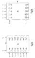
- solder ball pads 210are arranged on the circuit side 208 of the die 202 in a rectangular grid-like array as a plurality of columns (Cx) and rows (Rx), where x ranges upward from one until a number, dependent upon size of the solder ball pad and the size of the die, is reached where the die is filled.
- Cxcolumns
- Rxrows
- xranges upward from one until a number, dependent upon size of the solder ball pad and the size of the die, is reached where the die is filled.
- one embodiment of the present inventionlimits the number of solder ball pads on the die in a range from about 10 to about 30.
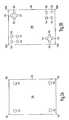
- solder ball pads 310are arranged on the circuit side 308 of the die 302 in corner regions 350 thereof.
- single solder ball padsare shown in the corner region while in FIG. 3B , pluralities of solder ball pads 310 are shown.
- corner regions 350 A and 350 Bthe plurality of solder ball pads are shown in a diamond-like arrangement as shown by the dashed lines.
- corner regions 350 C and 350 Dthe pluralities are shown in a square box-like arrangement. It should be appreciated that although described as corner-arranged solder ball pads, the pads themselves can still form one or more rows or columns of pads.
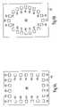
- the solder ball pads 410are arranged on the circuit side 408 of the die 402 about a perimeter or periphery of the die.
- the solder ball padsare arranged as a rectangular box-like configuration about the periphery of the die whereas in FIG. 4B , they are arranged in a oval-like configuration. It should be appreciated that although described as periphery-arranged solder ball pads, the pads themselves can still form one or more rows or columns of pads or occupy a corner region with one or more pads.
- solder ball pads 510are arranged on the circuit side 508 of the die 502 in a diagonal manner beginning in the corner regions 550 and extending linearly towards a center region 555 . It should be appreciated that although described as diagonally-arranged solder ball pads, the pads themselves can still form one or more rows or columns of pads, occupy a corner region or periphery with one or more pads.
- solder ball pads 610are arranged on the circuit side 608 of the die 602 in a crossly manner as indicated by the dashed lines that would cross one another somewhere in the vicinity of center region 655 . It should be appreciated that although described as crossly-arranged solder ball pads, the pads themselves can still form one or more rows or columns of pads, occupy a corner region or periphery with one or more pads.
- solder ball padswere arranged to generally avoid the center region of the particular die upon which it was placed. This is because as the die and the substrate are brought into proximity with one another to connect the solder balls to the substrate pads, the slots of the substrate generally exist above the center region of the dies. See FIG. 12 to understand this conceptually (slot 1224 is avoided by solder balls 1212 in corner regions of the dies 1202 ). As such, the solder ball pads are shown in a manner that avoids the slot of the substrate or, in other words, are disposed on the die not adjacent to the slot.
- the diewill have solder ball pads placed accordingly in other ways. Even further, in the event the substrates to which the dies are connected contain absolutely no slots the solder ball pad arrangement, and ultimately the solder ball arrangement, may exist anywhere on the surface of the die so long as the solder balls are electrically disconnected from the circuit.
- the present inventionmay be practiced with other well known packaging techniques.
- this techniqueit is possible to combine this technique with flip-chip packages.
- the inventive packagewould not only include electrically disconnected dummy solder balls for mounting purposes but would include solder balls or solder bumps electrically connected to the circuit of the die.
- dieswill be described as they are used in variety of applications. Some of these dies, it will be appreciated, are packaged in accordance with the foregoing described invention relating to electrically disconnected solder balls used for mounting purposes.
- the diesalso contain other integrated circuit elements such as capacitors, transistors, lines, interconnects, plugs, pads, I/O connections, insulators and other known elements as part of the die circuit previously mentioned.
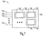
- circuit module 700may be a combination of dies 701 representing a variety of functions, or a combination of dies 701 containing the same functionality.
- circuit module 700includes at least one socket, slot, recess or the like 752 into which the die 701 is received.
- Slot 752in one embodiment is a circuit board 750 .
- Slot 752in another embodiment, represents a mount including land patterns.
- dies 701may be received by slot 752 in a pick-and-place operation by suitable pick-and-place machines.
- circuit module 700includes memory modules, device drivers, power modules, communication modems, processor modules and application-specific modules, and may include multilayer, multichip modules. Such modules will have a chip receiver in which a chip according to the present invention is inserted. Circuit module 700 may be a subcomponent of a variety of electronic systems, such as a clock, a television, a cell phone, a personal computer, an automobile, an industrial control system, an aircraft and others. Such modules will have a circuit module receiver in which a circuit module according to the present invention is inserted. Circuit module 700 will have a variety of leads 705 1 through 705 N extending therefrom providing unilateral or bilateral communication and control in its particular application.
- FIG. 8shows one embodiment of a circuit module as memory module 800 .
- Memory module 800contains multiple memory devices 801 contained on support 861 .
- support 861includes slots 852 for receiving memory devices 801 .
- the number of memory devicesgenerally depends upon the desired bus width and the desire for parity.
- Memory devices 801include at least die having electrically disconnected solder balls packaged in accordance with the present invention.
- the support 861includes sockets, slots, recesses or the like 852 , each adapted to receive a memory device 801 and provide electrical communication between a bus and memory device 801 .
- Memory module 800accepts a command signal from an external controller (not shown) on a command link 863 and provides for data input and data output on data links 865 .
- the command link 863 and data links 865are connected to leads 867 extending from the support 815 . Leads 867 are shown for conceptual purposes and are not limited to the position shown in FIG. 8 .
- FIG. 9shows one embodiment of an electronic system 900 containing one or more circuit modules 700 .
- At least one of the circuit modules 700contains a die having electrically disconnected solder balls packaged in accordance with the present invention.
- Electronic system 900generally contains a user interface 969 .
- User interface 969provides a user of the electronic system 900 with some form of control or observation of the results of the electronic system 900 .
- Some examples of user interface 969include the keyboard, pointing device, monitor or printer of a personal computer; the tuning dial, display or speakers of a radio; the ignition switch, gauges or gas pedal of an automobile; and the card reader, keypad, display or currency dispenser of an automated teller machine.
- User interface 969may further describe access ports provided to electronic system 900 .
- Access portsare used to connect an electronic system to the more tangible user interface components previously exemplified.
- One or more of the circuit modules 700may be a processor providing some form of manipulation, control or direction of inputs from or outputs to user interface 969 , or of other information either preprogrammed into, or otherwise provided to, electronic system 900 .
- electronic system 900includes memory modules 800 .
- electronic system 900will often be associated with certain mechanical components (not shown) in addition to circuit modules 700 and user interface 969 . It will be appreciated that the one or more circuit modules 700 in electronic system 900 can be replaced by a single integrated circuit.
- electronic system 900may be a subcomponent of a larger electronic system.
- FIG. 10shows one embodiment of an electronic system as memory system 1000 .
- Memory system 1000contains one or more memory modules 800 and a memory controller 1070 . At least one of the memory modules 800 includes a die having electrically disconnected solder balls packaged in accordance with the present invention.
- Memory controller 1070provides and controls a bidirectional interface between memory system 1000 and an external system bus 1072 .
- Memory system 1000accepts a command signal from the external bus 1072 and relays it to the one or more memory modules 800 on a command link 1074 .
- Memory system 1000provides for data input and data output between the one or more memory modules 800 and external system bus 1072 on data links 1076 .
- FIG. 11shows a further embodiment of an electronic system as a computer system 1100 .
- Computer system 1100contains a processor 1101 and a memory system 1000 housed in a computer unit 1080 .
- the memory system 1000includes a die packaged in accordance with the present invention.
- processor 1101includes a die packaged in accordance with the present invention.
- Computer system 1100is but one example of an electronic system containing another electronic system, i.e., memory system 1000 , as a subcomponent.
- Computer system 1100optionally contains user interface components. Depicted in FIG.
- a keyboard 1181a pointing device 1183 such as a mouse, trackball, or joystick
- a monitor 1185a printer 1187 and a bulk storage device 1189 .
- other componentsare often associated with computer system 1100 such as modems, device drivers, additional storage devices, etc.
- These other componentsinclude at least one die package having dummy solder balls of the present invention.
- the processor 1101 and memory system 1000 of computer system 1100can be incorporated on a single integrated circuit. Such single package processing units reduce the communication time between the processor and the memory circuit.
- packagesare taught that connect a plurality of solder balls between a plurality of solder ball pads of a die and substrate pads of a printed circuit board.
- the solder ballsare electrically disconnected from any circuit of the die and are used to temporarily hold the die in position with respect to the printed circuit board until the circuit is wire bonded and an underfill material is cured between the die and the printed circuit board to more permanently connect them together.
- the underfill materialis selected to have a coefficient of thermal expansion (CTE) that is substantially equal to the CTE of the solder balls. In this manner, the thermal mismatch of the prior art is avoided.
- the de-lamination problems associated with two-sided tapesare also avoided since the underfill material is selected to be better suited in joining a die with a printed circuit board.
- the packageis completed by disposing an overmolding compound about the die and the underfill material and about the wire bonds to protect the package from moisture, thermal swings, etc., in hostile environments.
Landscapes
- Engineering & Computer Science (AREA)
- Microelectronics & Electronic Packaging (AREA)
- Computer Hardware Design (AREA)
- Power Engineering (AREA)
- Physics & Mathematics (AREA)
- Condensed Matter Physics & Semiconductors (AREA)
- General Physics & Mathematics (AREA)
- Manufacturing & Machinery (AREA)
- Wire Bonding (AREA)
- Electric Connection Of Electric Components To Printed Circuits (AREA)
Abstract
Description
Claims (20)
Priority Applications (1)
| Application Number | Priority Date | Filing Date | Title |
|---|---|---|---|
| US12/022,211US7851907B2 (en) | 2002-04-15 | 2008-01-30 | Semiconductor integrated circuit package having electrically disconnected solder balls for mounting |
Applications Claiming Priority (3)
| Application Number | Priority Date | Filing Date | Title |
|---|---|---|---|
| US10/123,827US7276802B2 (en) | 2002-04-15 | 2002-04-15 | Semiconductor integrated circuit package having electrically disconnected solder balls for mounting |
| US11/428,625US7342319B2 (en) | 2002-04-15 | 2006-07-05 | Semiconductor integrated circuit package having electrically disconnected solder balls for mounting |
| US12/022,211US7851907B2 (en) | 2002-04-15 | 2008-01-30 | Semiconductor integrated circuit package having electrically disconnected solder balls for mounting |
Related Parent Applications (1)
| Application Number | Title | Priority Date | Filing Date |
|---|---|---|---|
| US11/428,625DivisionUS7342319B2 (en) | 2002-04-15 | 2006-07-05 | Semiconductor integrated circuit package having electrically disconnected solder balls for mounting |
Publications (2)
| Publication Number | Publication Date |
|---|---|
| US20080142950A1 US20080142950A1 (en) | 2008-06-19 |
| US7851907B2true US7851907B2 (en) | 2010-12-14 |
Family
ID=28790824
Family Applications (5)
| Application Number | Title | Priority Date | Filing Date |
|---|---|---|---|
| US10/123,827Expired - LifetimeUS7276802B2 (en) | 2002-04-15 | 2002-04-15 | Semiconductor integrated circuit package having electrically disconnected solder balls for mounting |
| US10/929,283Expired - LifetimeUS7268067B2 (en) | 2002-04-15 | 2004-08-30 | Semiconductor integrated circuit package having electrically disconnected solder balls for mounting |
| US11/428,625Expired - LifetimeUS7342319B2 (en) | 2002-04-15 | 2006-07-05 | Semiconductor integrated circuit package having electrically disconnected solder balls for mounting |
| US11/428,620Expired - LifetimeUS7468559B2 (en) | 2002-04-15 | 2006-07-05 | Semiconductor integrated circuit package having electrically disconnected solder balls for mounting |
| US12/022,211Expired - LifetimeUS7851907B2 (en) | 2002-04-15 | 2008-01-30 | Semiconductor integrated circuit package having electrically disconnected solder balls for mounting |
Family Applications Before (4)
| Application Number | Title | Priority Date | Filing Date |
|---|---|---|---|
| US10/123,827Expired - LifetimeUS7276802B2 (en) | 2002-04-15 | 2002-04-15 | Semiconductor integrated circuit package having electrically disconnected solder balls for mounting |
| US10/929,283Expired - LifetimeUS7268067B2 (en) | 2002-04-15 | 2004-08-30 | Semiconductor integrated circuit package having electrically disconnected solder balls for mounting |
| US11/428,625Expired - LifetimeUS7342319B2 (en) | 2002-04-15 | 2006-07-05 | Semiconductor integrated circuit package having electrically disconnected solder balls for mounting |
| US11/428,620Expired - LifetimeUS7468559B2 (en) | 2002-04-15 | 2006-07-05 | Semiconductor integrated circuit package having electrically disconnected solder balls for mounting |
Country Status (1)
| Country | Link |
|---|---|
| US (5) | US7276802B2 (en) |
Cited By (1)
| Publication number | Priority date | Publication date | Assignee | Title |
|---|---|---|---|---|
| US20180151528A1 (en)* | 2011-10-05 | 2018-05-31 | Taiwan Semiconductor Manufacturing Company, Ltd. | Packaging Structures of Integrated Circuits |
Families Citing this family (39)
| Publication number | Priority date | Publication date | Assignee | Title |
|---|---|---|---|---|
| US20040080056A1 (en)* | 2001-03-30 | 2004-04-29 | Lim David Chong Sook | Packaging system for die-up connection of a die-down oriented integrated circuit |
| US7276802B2 (en)* | 2002-04-15 | 2007-10-02 | Micron Technology, Inc. | Semiconductor integrated circuit package having electrically disconnected solder balls for mounting |
| US7182738B2 (en) | 2003-04-23 | 2007-02-27 | Marctec, Llc | Patient monitoring apparatus and method for orthosis and other devices |
| US7008854B2 (en) | 2003-05-21 | 2006-03-07 | Micron Technology, Inc. | Silicon oxycarbide substrates for bonded silicon on insulator |
| US7273788B2 (en) | 2003-05-21 | 2007-09-25 | Micron Technology, Inc. | Ultra-thin semiconductors bonded on glass substrates |
| US7153753B2 (en) | 2003-08-05 | 2006-12-26 | Micron Technology, Inc. | Strained Si/SiGe/SOI islands and processes of making same |
| US7262077B2 (en)* | 2003-09-30 | 2007-08-28 | Intel Corporation | Capillary underfill and mold encapsulation method and apparatus |
| US20050245062A1 (en)* | 2004-04-29 | 2005-11-03 | Jeff Kingsbury | Single row bond pad arrangement |
| KR100632807B1 (en)* | 2004-11-26 | 2006-10-16 | 삼성전자주식회사 | Semiconductor chip and tab package containing same |
| US7408786B2 (en)* | 2005-06-13 | 2008-08-05 | Research In Motion Limited | Electrical connector and system for a component in an electronic device |
| US7835158B2 (en)* | 2005-12-30 | 2010-11-16 | Micron Technology, Inc. | Connection verification technique |
| SG135074A1 (en) | 2006-02-28 | 2007-09-28 | Micron Technology Inc | Microelectronic devices, stacked microelectronic devices, and methods for manufacturing such devices |
| JP4758787B2 (en)* | 2006-03-02 | 2011-08-31 | パナソニック株式会社 | Semiconductor integrated circuit |
| US7714453B2 (en) | 2006-05-12 | 2010-05-11 | Broadcom Corporation | Interconnect structure and formation for package stacking of molded plastic area array package |
| US8581381B2 (en)* | 2006-06-20 | 2013-11-12 | Broadcom Corporation | Integrated circuit (IC) package stacking and IC packages formed by same |
| US20080160173A1 (en)* | 2006-12-27 | 2008-07-03 | Nokia Corporation | Component Moulding Process |
| US8390107B2 (en) | 2007-09-28 | 2013-03-05 | Intel Mobile Communications GmbH | Semiconductor device and methods of manufacturing semiconductor devices |
| US7906860B2 (en)* | 2007-10-26 | 2011-03-15 | Infineon Technologies Ag | Semiconductor device |
| US8116097B2 (en)* | 2007-11-02 | 2012-02-14 | Oracle America, Inc. | Apparatus for electrically coupling a semiconductor package to a printed circuit board |
| US10074553B2 (en)* | 2007-12-03 | 2018-09-11 | STATS ChipPAC Pte. Ltd. | Wafer level package integration and method |
| US9460951B2 (en)* | 2007-12-03 | 2016-10-04 | STATS ChipPAC Pte. Ltd. | Semiconductor device and method of wafer level package integration |
| US7683495B2 (en)* | 2008-02-27 | 2010-03-23 | Broadcom Corporation | Integrated circuit package substrate having configurable bond pads |
| US8350383B2 (en)* | 2009-07-16 | 2013-01-08 | International Business Machines Corporation | IC chip package having IC chip with overhang and/or BGA blocking underfill material flow and related methods |
| KR101192181B1 (en) | 2010-03-31 | 2012-10-17 | (주)포인트엔지니어링 | Optical Element Device and Fabricating Method Thereof |
| US9258670B2 (en) | 2011-06-10 | 2016-02-09 | Aliphcom | Wireless enabled cap for a data-capable device |
| US8446275B2 (en) | 2011-06-10 | 2013-05-21 | Aliphcom | General health and wellness management method and apparatus for a wellness application using data from a data-capable band |
| US20120313296A1 (en)* | 2011-06-10 | 2012-12-13 | Aliphcom | Component protective overmolding |
| JPWO2013133122A1 (en)* | 2012-03-07 | 2015-07-30 | 三菱電機株式会社 | High frequency package |
| US20150092360A1 (en)* | 2013-10-01 | 2015-04-02 | Nike, Inc. | Battery overmolding |
| US9847462B2 (en) | 2013-10-29 | 2017-12-19 | Point Engineering Co., Ltd. | Array substrate for mounting chip and method for manufacturing the same |
| TWI539565B (en)* | 2014-01-29 | 2016-06-21 | 森富科技股份有限公司 | Memory and layout method of memory ball pads |
| US9837278B2 (en)* | 2014-02-27 | 2017-12-05 | Taiwan Semiconductor Manufacturing Company Ltd. | Wafer level chip scale package and method of manufacturing the same |
| DE112014006844T5 (en)* | 2014-07-28 | 2017-04-13 | GM Global Technology Operations LLC | Reinforced gluing systems and methods |
| US9666558B2 (en) | 2015-06-29 | 2017-05-30 | Point Engineering Co., Ltd. | Substrate for mounting a chip and chip package using the substrate |
| US10971468B2 (en) | 2016-11-21 | 2021-04-06 | 3M Innovative Properties Company | Automatic registration between circuit dies and interconnects |
| US20190311983A1 (en)* | 2016-12-27 | 2019-10-10 | Intel Corporation | Stacking multiple dies having dissimilar interconnect structure layout and pitch |
| CN112382618B (en)* | 2020-11-09 | 2023-10-27 | 成都海光集成电路设计有限公司 | Packaging structure and packaging method |
| KR20220151307A (en) | 2021-05-06 | 2022-11-15 | 삼성전자주식회사 | Semiconductor package and method of manufacturing the semiconductor package |
| CN113643998B (en)* | 2021-08-02 | 2024-03-26 | 东莞先导先进科技有限公司 | Semiconductor package testing system and method |
Citations (63)
| Publication number | Priority date | Publication date | Assignee | Title |
|---|---|---|---|---|
| US5311059A (en) | 1992-01-24 | 1994-05-10 | Motorola, Inc. | Backplane grounding for flip-chip integrated circuit |
| US5400950A (en)* | 1994-02-22 | 1995-03-28 | Delco Electronics Corporation | Method for controlling solder bump height for flip chip integrated circuit devices |
| US5410181A (en) | 1994-06-20 | 1995-04-25 | Motorola, Inc. | Assembly for mounting an electronic device having an optically erasable surface |
| JPH09232375A (en) | 1996-02-19 | 1997-09-05 | Nec Corp | Semiconductor device |
| US5748450A (en) | 1995-10-19 | 1998-05-05 | Lg Semicon Co., Ltd. | BGA package using a dummy ball and a repairing method thereof |
| US5811317A (en) | 1995-08-25 | 1998-09-22 | Texas Instruments Incorporated | Process for reflow bonding a semiconductor die to a substrate and the product produced by the product |
| US5898224A (en) | 1997-01-24 | 1999-04-27 | Micron Technology, Inc. | Apparatus for packaging flip chip bare die on printed circuit boards |
| USRE36325E (en) | 1988-09-30 | 1999-10-05 | Micron Technology, Inc. | Directly bonded SIMM module |
| US5994166A (en) | 1997-03-10 | 1999-11-30 | Micron Technology, Inc. | Method of constructing stacked packages |
| US6008071A (en)* | 1995-09-20 | 1999-12-28 | Fujitsu Limited | Method of forming solder bumps onto an integrated circuit device |
| US6048755A (en) | 1998-11-12 | 2000-04-11 | Micron Technology, Inc. | Method for fabricating BGA package using substrate with patterned solder mask open in die attach area |
| GB2345191A (en) | 1998-12-22 | 2000-06-28 | Nec Corp | Mounting semiconductor packages on substrates |
| US6084297A (en) | 1998-09-03 | 2000-07-04 | Micron Technology, Inc. | Cavity ball grid array apparatus |
| US6121576A (en) | 1998-09-02 | 2000-09-19 | Micron Technology, Inc. | Method and process of contact to a heat softened solder ball array |
| US6127724A (en) | 1996-10-31 | 2000-10-03 | Tessera, Inc. | Packaged microelectronic elements with enhanced thermal conduction |
| US6150724A (en)* | 1998-03-02 | 2000-11-21 | Motorola, Inc. | Multi-chip semiconductor device and method for making the device by using multiple flip chip interfaces |
| US6160715A (en) | 1998-09-08 | 2000-12-12 | Lucent Technologies Inc. | Translator for recessed flip-chip package |
| US6175157B1 (en) | 1997-03-21 | 2001-01-16 | Rohm Co., Ltd. | Semiconductor device package for suppressing warping in semiconductor chips |
| US6198162B1 (en) | 1995-10-12 | 2001-03-06 | Micron Technology, Inc. | Method and apparatus for a chip-on-board semiconductor module |
| US6208156B1 (en) | 1998-09-03 | 2001-03-27 | Micron Technology, Inc. | Test carrier for packaging semiconductor components having contact balls and calibration carrier for calibrating semiconductor test systems |
| KR20010027290A (en) | 1999-09-13 | 2001-04-06 | 윤종용 | Method for fabricating a chip scale type semiconductor package |
| US6214716B1 (en) | 1998-09-30 | 2001-04-10 | Micron Technology, Inc. | Semiconductor substrate-based BGA interconnection and methods of farication same |
| US6225702B1 (en) | 1997-08-29 | 2001-05-01 | Mitsubishi Denki Kabushiki Kaisha | Ball grid array to prevent shorting between a power supply and ground terminal |
| US6232666B1 (en) | 1998-12-04 | 2001-05-15 | Mciron Technology, Inc. | Interconnect for packaging semiconductor dice and fabricating BGA packages |
| US6258626B1 (en) | 2000-07-06 | 2001-07-10 | Advanced Semiconductor Engineering, Inc. | Method of making stacked chip package |
| US6391762B1 (en) | 1999-11-12 | 2002-05-21 | Motorola, Inc. | Method of forming a microelectronic assembly with a particulate free underfill material and a microelectronic assembly incorporation the same |
| US6400574B1 (en) | 2000-05-11 | 2002-06-04 | Micron Technology, Inc. | Molded ball grid array |
| US20020096784A1 (en)* | 2001-01-15 | 2002-07-25 | Koichi Kamikuri | Semiconductor device and semiconductor device structure |
| US20020100976A1 (en) | 2001-01-30 | 2002-08-01 | Hui Chong Chin | BOC semiconductor package including a semiconductor die and a substrate bonded circuit side down to the die |
| US20020114135A1 (en) | 1999-07-30 | 2002-08-22 | Salman Akram | Heat sink chip package |
| US6462420B2 (en) | 1999-02-12 | 2002-10-08 | Rohm Co., Ltd. | Semiconductor chip and semiconductor device having a chip-on-chip structure |
| US20020149298A1 (en) | 1995-06-30 | 2002-10-17 | Kabushiki Kaisha Toshiba | Electronic component and method of production thereof |
| US20020167077A1 (en) | 2001-05-08 | 2002-11-14 | International Business Machines Corporation | Flip-chip package with underfill having low density filler |
| US20020187590A1 (en) | 2000-08-31 | 2002-12-12 | Micron Technology, Inc. | Ball grid array packages with thermally conductive containers |
| US20020195718A1 (en) | 1997-03-27 | 2002-12-26 | Hitachi, Ltd. | Process for mounting electronic device and semiconductor device |
| US6500764B1 (en) | 2001-10-29 | 2002-12-31 | Fairchild Semiconductor Corporation | Method for thinning a semiconductor substrate |
| US20030027377A1 (en) | 1994-12-05 | 2003-02-06 | Owens Norman Lee | Multi-strand substrate for ball-grid array assemblies and method |
| US6522018B1 (en) | 2000-05-16 | 2003-02-18 | Micron Technology, Inc. | Ball grid array chip packages having improved testing and stacking characteristics |
| US6533159B1 (en) | 1998-10-07 | 2003-03-18 | Micron Technology, Inc. | Apparatus for attaching solder balls to BGA package utilizing a tool to pick and dip the solder ball in flux |
| US6576495B1 (en) | 2000-08-30 | 2003-06-10 | Micron Technology, Inc. | Microelectronic assembly with pre-disposed fill material and associated method of manufacture |
| US6576496B1 (en) | 2000-08-21 | 2003-06-10 | Micron Technology, Inc. | Method and apparatus for encapsulating a multi-chip substrate array |
| US6577004B1 (en) | 2000-08-31 | 2003-06-10 | Micron Technology, Inc. | Solder ball landpad design to improve laminate performance |
| US6583502B2 (en) | 2001-04-17 | 2003-06-24 | Micron Technology, Inc. | Apparatus for package reduction in stacked chip and board assemblies |
| US20030116866A1 (en) | 2001-12-20 | 2003-06-26 | Cher 'khng Victor Tan | Semiconductor package having substrate with multi-layer metal bumps |
| US6603071B2 (en) | 2000-07-05 | 2003-08-05 | Sharp Kabushiki Kaisha | Flexible printed circuit board, integrated circuit chip mounting flexible printed circuit board, display apparatus incorporating, integrated circuit chip mounted structure, and bonding method of integrated circuit chip mounting flexible printed circuit board |
| US6602733B2 (en) | 2000-02-18 | 2003-08-05 | Sony Corporation | Method for fabricating electronic circuit device, semiconductor device and electronic circuit device including bump bonding |
| JP2003234435A (en) | 2002-02-06 | 2003-08-22 | Nec Saitama Ltd | Semiconductor integrated circuit package |
| US20030193088A1 (en) | 2002-04-15 | 2003-10-16 | Micron Technology, Inc. | Semiconductor integrated circuit package having electrically disconnected solder balls for mounting |
| US6660558B1 (en) | 1999-12-16 | 2003-12-09 | Micron Technology, Inc. | Semiconductor package with molded flash |
| US20040004292A1 (en) | 2002-07-05 | 2004-01-08 | Industrial Technology Research Institute | Method for bonding IC chips to substrates incorporating dummy bumps and non-conductive adhesive and structures formed |
| US6680213B2 (en) | 2001-04-02 | 2004-01-20 | Micron Technology, Inc. | Method and system for fabricating contacts on semiconductor components |
| US6687989B1 (en) | 1998-07-06 | 2004-02-10 | Micron Technology, Inc. | Method for fabricating interconnect having support members for preventing component flexure |
| US6700183B2 (en) | 2001-02-23 | 2004-03-02 | Micron Technology, Inc. | Low temperature die attaching material for BOC packages and products comprising such material |
| US6724084B1 (en) | 1999-02-08 | 2004-04-20 | Rohm Co., Ltd. | Semiconductor chip and production thereof, and semiconductor device having semiconductor chip bonded to solid device |
| US20040084771A1 (en) | 2002-11-05 | 2004-05-06 | Micron Technology, Inc. | Methods and apparatus for a thin stacked ball-grid array package |
| US6736306B2 (en) | 2001-02-05 | 2004-05-18 | Samsung Electronics Co., Ltd. | Semiconductor chip package comprising enhanced pads |
| US6750552B1 (en) | 2002-12-18 | 2004-06-15 | Netlogic Microsystems, Inc. | Integrated circuit package with solder bumps |
| US6762495B1 (en) | 2003-01-30 | 2004-07-13 | Qualcomm Incorporated | Area array package with non-electrically connected solder balls |
| US6778404B1 (en) | 2000-06-02 | 2004-08-17 | Micron Technology Inc | Stackable ball grid array |
| US6781245B2 (en) | 2001-01-08 | 2004-08-24 | Siliconware Precision Industries Co., Ltd. | Array structure of solder balls able to control collapse |
| US20040200885A1 (en) | 2001-08-24 | 2004-10-14 | Derderian James M | Methods for assembling semiconductor devices in stacked arrangements by positioning spacers therebetween |
| US20040212067A1 (en) | 2003-04-25 | 2004-10-28 | Advanced Semiconductor Engineering, Inc. | Multi-chips stacked package |
| US6889430B2 (en) | 2000-07-31 | 2005-05-10 | Micron Technology, Inc. | Method of selectively adjusting surface tension of soldermask material |
Family Cites Families (1)
| Publication number | Priority date | Publication date | Assignee | Title |
|---|---|---|---|---|
| US6453563B1 (en)* | 2001-01-05 | 2002-09-24 | Hyde Manufacturing Company, Inc. | Hand tool handle |
- 2002
- 2002-04-15USUS10/123,827patent/US7276802B2/ennot_activeExpired - Lifetime
- 2004
- 2004-08-30USUS10/929,283patent/US7268067B2/ennot_activeExpired - Lifetime
- 2006
- 2006-07-05USUS11/428,625patent/US7342319B2/ennot_activeExpired - Lifetime
- 2006-07-05USUS11/428,620patent/US7468559B2/ennot_activeExpired - Lifetime
- 2008
- 2008-01-30USUS12/022,211patent/US7851907B2/ennot_activeExpired - Lifetime
Patent Citations (87)
| Publication number | Priority date | Publication date | Assignee | Title |
|---|---|---|---|---|
| USRE36325E (en) | 1988-09-30 | 1999-10-05 | Micron Technology, Inc. | Directly bonded SIMM module |
| US5311059A (en) | 1992-01-24 | 1994-05-10 | Motorola, Inc. | Backplane grounding for flip-chip integrated circuit |
| US5400950A (en)* | 1994-02-22 | 1995-03-28 | Delco Electronics Corporation | Method for controlling solder bump height for flip chip integrated circuit devices |
| US5410181A (en) | 1994-06-20 | 1995-04-25 | Motorola, Inc. | Assembly for mounting an electronic device having an optically erasable surface |
| US20030027377A1 (en) | 1994-12-05 | 2003-02-06 | Owens Norman Lee | Multi-strand substrate for ball-grid array assemblies and method |
| US20020149298A1 (en) | 1995-06-30 | 2002-10-17 | Kabushiki Kaisha Toshiba | Electronic component and method of production thereof |
| US5811317A (en) | 1995-08-25 | 1998-09-22 | Texas Instruments Incorporated | Process for reflow bonding a semiconductor die to a substrate and the product produced by the product |
| US6008071A (en)* | 1995-09-20 | 1999-12-28 | Fujitsu Limited | Method of forming solder bumps onto an integrated circuit device |
| US6198162B1 (en) | 1995-10-12 | 2001-03-06 | Micron Technology, Inc. | Method and apparatus for a chip-on-board semiconductor module |
| US5748450A (en) | 1995-10-19 | 1998-05-05 | Lg Semicon Co., Ltd. | BGA package using a dummy ball and a repairing method thereof |
| JPH09232375A (en) | 1996-02-19 | 1997-09-05 | Nec Corp | Semiconductor device |
| US6127724A (en) | 1996-10-31 | 2000-10-03 | Tessera, Inc. | Packaged microelectronic elements with enhanced thermal conduction |
| US5898224A (en) | 1997-01-24 | 1999-04-27 | Micron Technology, Inc. | Apparatus for packaging flip chip bare die on printed circuit boards |
| US6661103B2 (en) | 1997-01-24 | 2003-12-09 | Micron Technology, Inc. | Apparatus for packaging flip chip bare die on printed circuit boards |
| US6051878A (en) | 1997-03-10 | 2000-04-18 | Micron Technology, Inc. | Method of constructing stacked packages |
| US6222265B1 (en) | 1997-03-10 | 2001-04-24 | Micron Technology, Inc. | Method of constructing stacked packages |
| US5994166A (en) | 1997-03-10 | 1999-11-30 | Micron Technology, Inc. | Method of constructing stacked packages |
| US6175157B1 (en) | 1997-03-21 | 2001-01-16 | Rohm Co., Ltd. | Semiconductor device package for suppressing warping in semiconductor chips |
| US20020195718A1 (en) | 1997-03-27 | 2002-12-26 | Hitachi, Ltd. | Process for mounting electronic device and semiconductor device |
| US6225702B1 (en) | 1997-08-29 | 2001-05-01 | Mitsubishi Denki Kabushiki Kaisha | Ball grid array to prevent shorting between a power supply and ground terminal |
| US6150724A (en)* | 1998-03-02 | 2000-11-21 | Motorola, Inc. | Multi-chip semiconductor device and method for making the device by using multiple flip chip interfaces |
| US6687989B1 (en) | 1998-07-06 | 2004-02-10 | Micron Technology, Inc. | Method for fabricating interconnect having support members for preventing component flexure |
| US6121576A (en) | 1998-09-02 | 2000-09-19 | Micron Technology, Inc. | Method and process of contact to a heat softened solder ball array |
| US6329637B1 (en) | 1998-09-02 | 2001-12-11 | Micron Technology, Inc. | Method and process of contract to a heat softened solder ball array |
| US6208156B1 (en) | 1998-09-03 | 2001-03-27 | Micron Technology, Inc. | Test carrier for packaging semiconductor components having contact balls and calibration carrier for calibrating semiconductor test systems |
| US6504389B1 (en) | 1998-09-03 | 2003-01-07 | Micron Technology, Inc. | Test carrier for packaging semiconductor components having contact balls and calibration carrier for calibrating semiconductor test systems |
| US6084297A (en) | 1998-09-03 | 2000-07-04 | Micron Technology, Inc. | Cavity ball grid array apparatus |
| US6326244B1 (en) | 1998-09-03 | 2001-12-04 | Micron Technology, Inc. | Method of making a cavity ball grid array apparatus |
| US6160715A (en) | 1998-09-08 | 2000-12-12 | Lucent Technologies Inc. | Translator for recessed flip-chip package |
| US6214716B1 (en) | 1998-09-30 | 2001-04-10 | Micron Technology, Inc. | Semiconductor substrate-based BGA interconnection and methods of farication same |
| US6599822B1 (en) | 1998-09-30 | 2003-07-29 | Micron Technology, Inc. | Methods of fabricating semiconductor substrate-based BGA interconnection |
| US6646286B1 (en) | 1998-09-30 | 2003-11-11 | Micron Technology, Inc. | Semiconductor substrate-based BGA interconnection |
| US6533159B1 (en) | 1998-10-07 | 2003-03-18 | Micron Technology, Inc. | Apparatus for attaching solder balls to BGA package utilizing a tool to pick and dip the solder ball in flux |
| US6595408B1 (en) | 1998-10-07 | 2003-07-22 | Micron Technology, Inc. | Method of attaching solder balls to BGA package utilizing a tool to pick and dip the solder ball in flux prior to placement |
| US6048755A (en) | 1998-11-12 | 2000-04-11 | Micron Technology, Inc. | Method for fabricating BGA package using substrate with patterned solder mask open in die attach area |
| US6825569B2 (en) | 1998-11-12 | 2004-11-30 | Micron Technology, Inc. | BGA package having substrate with patterned solder mask defining open die attach area |
| US6232666B1 (en) | 1998-12-04 | 2001-05-15 | Mciron Technology, Inc. | Interconnect for packaging semiconductor dice and fabricating BGA packages |
| US6329222B1 (en) | 1998-12-04 | 2001-12-11 | Micron Technology, Inc. | Interconnect for packaging semiconductor dice and fabricating BGA packages |
| GB2345191A (en) | 1998-12-22 | 2000-06-28 | Nec Corp | Mounting semiconductor packages on substrates |
| US6724084B1 (en) | 1999-02-08 | 2004-04-20 | Rohm Co., Ltd. | Semiconductor chip and production thereof, and semiconductor device having semiconductor chip bonded to solid device |
| US6462420B2 (en) | 1999-02-12 | 2002-10-08 | Rohm Co., Ltd. | Semiconductor chip and semiconductor device having a chip-on-chip structure |
| US20020114135A1 (en) | 1999-07-30 | 2002-08-22 | Salman Akram | Heat sink chip package |
| KR20010027290A (en) | 1999-09-13 | 2001-04-06 | 윤종용 | Method for fabricating a chip scale type semiconductor package |
| US6391762B1 (en) | 1999-11-12 | 2002-05-21 | Motorola, Inc. | Method of forming a microelectronic assembly with a particulate free underfill material and a microelectronic assembly incorporation the same |
| US6660558B1 (en) | 1999-12-16 | 2003-12-09 | Micron Technology, Inc. | Semiconductor package with molded flash |
| US6602733B2 (en) | 2000-02-18 | 2003-08-05 | Sony Corporation | Method for fabricating electronic circuit device, semiconductor device and electronic circuit device including bump bonding |
| US6503781B2 (en) | 2000-05-11 | 2003-01-07 | Micron Technology, Inc. | Molded ball grid array |
| US6400574B1 (en) | 2000-05-11 | 2002-06-04 | Micron Technology, Inc. | Molded ball grid array |
| US6600335B2 (en) | 2000-05-16 | 2003-07-29 | Micron Technology, Inc. | Method for ball grid array chip packages having improved testing and stacking characteristics |
| US6522018B1 (en) | 2000-05-16 | 2003-02-18 | Micron Technology, Inc. | Ball grid array chip packages having improved testing and stacking characteristics |
| US6778404B1 (en) | 2000-06-02 | 2004-08-17 | Micron Technology Inc | Stackable ball grid array |
| US20050019983A1 (en) | 2000-06-02 | 2005-01-27 | Bolken Todd O. | Method of manufacturing a stackable ball grid array |
| US20040164412A1 (en) | 2000-06-02 | 2004-08-26 | Bolken Todd O. | Stackable ball grid array |
| US6603071B2 (en) | 2000-07-05 | 2003-08-05 | Sharp Kabushiki Kaisha | Flexible printed circuit board, integrated circuit chip mounting flexible printed circuit board, display apparatus incorporating, integrated circuit chip mounted structure, and bonding method of integrated circuit chip mounting flexible printed circuit board |
| US6258626B1 (en) | 2000-07-06 | 2001-07-10 | Advanced Semiconductor Engineering, Inc. | Method of making stacked chip package |
| US6889430B2 (en) | 2000-07-31 | 2005-05-10 | Micron Technology, Inc. | Method of selectively adjusting surface tension of soldermask material |
| US6576496B1 (en) | 2000-08-21 | 2003-06-10 | Micron Technology, Inc. | Method and apparatus for encapsulating a multi-chip substrate array |
| US6661104B2 (en)* | 2000-08-30 | 2003-12-09 | Micron Technology, Inc. | Microelectronic assembly with pre-disposed fill material and associated method of manufacture |
| US6576495B1 (en) | 2000-08-30 | 2003-06-10 | Micron Technology, Inc. | Microelectronic assembly with pre-disposed fill material and associated method of manufacture |
| US6559537B1 (en) | 2000-08-31 | 2003-05-06 | Micron Technology, Inc. | Ball grid array packages with thermally conductive containers |
| US6577004B1 (en) | 2000-08-31 | 2003-06-10 | Micron Technology, Inc. | Solder ball landpad design to improve laminate performance |
| US20020187590A1 (en) | 2000-08-31 | 2002-12-12 | Micron Technology, Inc. | Ball grid array packages with thermally conductive containers |
| US6781245B2 (en) | 2001-01-08 | 2004-08-24 | Siliconware Precision Industries Co., Ltd. | Array structure of solder balls able to control collapse |
| US20020096784A1 (en)* | 2001-01-15 | 2002-07-25 | Koichi Kamikuri | Semiconductor device and semiconductor device structure |
| US20020100976A1 (en) | 2001-01-30 | 2002-08-01 | Hui Chong Chin | BOC semiconductor package including a semiconductor die and a substrate bonded circuit side down to the die |
| US6507114B2 (en) | 2001-01-30 | 2003-01-14 | Micron Technology, Inc. | BOC semiconductor package including a semiconductor die and a substrate bonded circuit side down to the die |
| US6638792B2 (en) | 2001-01-30 | 2003-10-28 | Micron Technology, Inc. | Method for fabricating BOC semiconductor package |
| US6736306B2 (en) | 2001-02-05 | 2004-05-18 | Samsung Electronics Co., Ltd. | Semiconductor chip package comprising enhanced pads |
| US6700183B2 (en) | 2001-02-23 | 2004-03-02 | Micron Technology, Inc. | Low temperature die attaching material for BOC packages and products comprising such material |
| US6680213B2 (en) | 2001-04-02 | 2004-01-20 | Micron Technology, Inc. | Method and system for fabricating contacts on semiconductor components |
| US6583502B2 (en) | 2001-04-17 | 2003-06-24 | Micron Technology, Inc. | Apparatus for package reduction in stacked chip and board assemblies |
| US20020167077A1 (en) | 2001-05-08 | 2002-11-14 | International Business Machines Corporation | Flip-chip package with underfill having low density filler |
| US20040200885A1 (en) | 2001-08-24 | 2004-10-14 | Derderian James M | Methods for assembling semiconductor devices in stacked arrangements by positioning spacers therebetween |
| US6500764B1 (en) | 2001-10-29 | 2002-12-31 | Fairchild Semiconductor Corporation | Method for thinning a semiconductor substrate |
| US20030116866A1 (en) | 2001-12-20 | 2003-06-26 | Cher 'khng Victor Tan | Semiconductor package having substrate with multi-layer metal bumps |
| JP2003234435A (en) | 2002-02-06 | 2003-08-22 | Nec Saitama Ltd | Semiconductor integrated circuit package |
| US20030193088A1 (en) | 2002-04-15 | 2003-10-16 | Micron Technology, Inc. | Semiconductor integrated circuit package having electrically disconnected solder balls for mounting |
| US20050026327A1 (en) | 2002-04-15 | 2005-02-03 | Micron Technology, Inc. | Semiconductor integrated circuit package having electrically disconnected solder balls for mounting |
| US7268067B2 (en) | 2002-04-15 | 2007-09-11 | Micron Technology, Inc. | Semiconductor integrated circuit package having electrically disconnected solder balls for mounting |
| US7276802B2 (en) | 2002-04-15 | 2007-10-02 | Micron Technology, Inc. | Semiconductor integrated circuit package having electrically disconnected solder balls for mounting |
| US7342319B2 (en) | 2002-04-15 | 2008-03-11 | Micron Technology, Inc. | Semiconductor integrated circuit package having electrically disconnected solder balls for mounting |
| US7468559B2 (en) | 2002-04-15 | 2008-12-23 | Micron Technology, Inc. | Semiconductor integrated circuit package having electrically disconnected solder balls for mounting |
| US20040004292A1 (en) | 2002-07-05 | 2004-01-08 | Industrial Technology Research Institute | Method for bonding IC chips to substrates incorporating dummy bumps and non-conductive adhesive and structures formed |
| US20040084771A1 (en) | 2002-11-05 | 2004-05-06 | Micron Technology, Inc. | Methods and apparatus for a thin stacked ball-grid array package |
| US6750552B1 (en) | 2002-12-18 | 2004-06-15 | Netlogic Microsystems, Inc. | Integrated circuit package with solder bumps |
| US6762495B1 (en) | 2003-01-30 | 2004-07-13 | Qualcomm Incorporated | Area array package with non-electrically connected solder balls |
| US20040212067A1 (en) | 2003-04-25 | 2004-10-28 | Advanced Semiconductor Engineering, Inc. | Multi-chips stacked package |
Non-Patent Citations (1)
| Title |
|---|
| Fan, L. , et al., "Incorporation of Inorganic Filler into the No-Flow Underfill Material for Flip-Chip Application", International Symposium on Advanced Packaging Materials,(2000),303-310. |
Cited By (2)
| Publication number | Priority date | Publication date | Assignee | Title |
|---|---|---|---|---|
| US20180151528A1 (en)* | 2011-10-05 | 2018-05-31 | Taiwan Semiconductor Manufacturing Company, Ltd. | Packaging Structures of Integrated Circuits |
| US10453818B2 (en)* | 2011-10-05 | 2019-10-22 | Taiwan Semiconductor Manufacturing Company, Ltd. | Packaging structures of integrated circuits |
Also Published As
| Publication number | Publication date |
|---|---|
| US20030193088A1 (en) | 2003-10-16 |
| US7468559B2 (en) | 2008-12-23 |
| US7268067B2 (en) | 2007-09-11 |
| US20050026327A1 (en) | 2005-02-03 |
| US7342319B2 (en) | 2008-03-11 |
| US20060237845A1 (en) | 2006-10-26 |
| US20060237844A1 (en) | 2006-10-26 |
| US7276802B2 (en) | 2007-10-02 |
| US20080142950A1 (en) | 2008-06-19 |
Similar Documents
| Publication | Publication Date | Title |
|---|---|---|
| US7851907B2 (en) | Semiconductor integrated circuit package having electrically disconnected solder balls for mounting | |
| US7148560B2 (en) | IC chip package structure and underfill process | |
| KR100621991B1 (en) | Chip Scale Stacking Package | |
| US9269695B2 (en) | Semiconductor device assemblies including face-to-face semiconductor dice and related methods | |
| US7074696B1 (en) | Semiconductor circuit module and method for fabricating semiconductor circuit modules | |
| KR101805114B1 (en) | Integrated circuit packaging system with dual side connection and method of manufacture thereof | |
| US7911068B2 (en) | Component and method for producing a component | |
| US6667191B1 (en) | Chip scale integrated circuit package | |
| US6919645B2 (en) | Die package | |
| KR20100037300A (en) | Method of forming semiconductor device having embedded interposer | |
| US7317251B2 (en) | Multichip module including a plurality of semiconductor chips, and printed circuit board including a plurality of components | |
| US7847386B1 (en) | Reduced size stacked semiconductor package and method of making the same | |
| US20180130757A1 (en) | Folding thin systems | |
| US8872318B2 (en) | Through interposer wire bond using low CTE interposer with coarse slot apertures | |
| EP1212791A1 (en) | Method and structure for manufacturing improved yield semiconductor packaged devices | |
| US20060102998A1 (en) | Flip-chip component | |
| US20040259290A1 (en) | Method for improving the mechanical properties of BOC module arrangements | |
| KR100546359B1 (en) | Semiconductor chip package and stacked module including functional part and mounting part arranged laterally on the same plane | |
| US20040224481A1 (en) | Semiconductor devices, manufacturing methods therefor, circuit substrates and electronic devices | |
| US20070228580A1 (en) | Semiconductor device having stacked structure and method of manufacturing the same | |
| US20040089930A1 (en) | Simplified stacked chip assemblies | |
| KR100650763B1 (en) | Stacked Package | |
| KR20140083586A (en) | Semiconductor package using of silicon interposer and the method |
Legal Events
| Date | Code | Title | Description |
|---|---|---|---|
| STCF | Information on status: patent grant | Free format text:PATENTED CASE | |
| FEPP | Fee payment procedure | Free format text:PAYOR NUMBER ASSIGNED (ORIGINAL EVENT CODE: ASPN); ENTITY STATUS OF PATENT OWNER: LARGE ENTITY | |
| FPAY | Fee payment | Year of fee payment:4 | |
| AS | Assignment | Owner name:U.S. BANK NATIONAL ASSOCIATION, AS COLLATERAL AGENT, CALIFORNIA Free format text:SECURITY INTEREST;ASSIGNOR:MICRON TECHNOLOGY, INC.;REEL/FRAME:038669/0001 Effective date:20160426 Owner name:U.S. BANK NATIONAL ASSOCIATION, AS COLLATERAL AGEN Free format text:SECURITY INTEREST;ASSIGNOR:MICRON TECHNOLOGY, INC.;REEL/FRAME:038669/0001 Effective date:20160426 | |
| AS | Assignment | Owner name:MORGAN STANLEY SENIOR FUNDING, INC., AS COLLATERAL AGENT, MARYLAND Free format text:PATENT SECURITY AGREEMENT;ASSIGNOR:MICRON TECHNOLOGY, INC.;REEL/FRAME:038954/0001 Effective date:20160426 Owner name:MORGAN STANLEY SENIOR FUNDING, INC., AS COLLATERAL Free format text:PATENT SECURITY AGREEMENT;ASSIGNOR:MICRON TECHNOLOGY, INC.;REEL/FRAME:038954/0001 Effective date:20160426 | |
| AS | Assignment | Owner name:U.S. BANK NATIONAL ASSOCIATION, AS COLLATERAL AGENT, CALIFORNIA Free format text:CORRECTIVE ASSIGNMENT TO CORRECT THE REPLACE ERRONEOUSLY FILED PATENT #7358718 WITH THE CORRECT PATENT #7358178 PREVIOUSLY RECORDED ON REEL 038669 FRAME 0001. ASSIGNOR(S) HEREBY CONFIRMS THE SECURITY INTEREST;ASSIGNOR:MICRON TECHNOLOGY, INC.;REEL/FRAME:043079/0001 Effective date:20160426 Owner name:U.S. BANK NATIONAL ASSOCIATION, AS COLLATERAL AGEN Free format text:CORRECTIVE ASSIGNMENT TO CORRECT THE REPLACE ERRONEOUSLY FILED PATENT #7358718 WITH THE CORRECT PATENT #7358178 PREVIOUSLY RECORDED ON REEL 038669 FRAME 0001. ASSIGNOR(S) HEREBY CONFIRMS THE SECURITY INTEREST;ASSIGNOR:MICRON TECHNOLOGY, INC.;REEL/FRAME:043079/0001 Effective date:20160426 | |
| MAFP | Maintenance fee payment | Free format text:PAYMENT OF MAINTENANCE FEE, 8TH YEAR, LARGE ENTITY (ORIGINAL EVENT CODE: M1552) Year of fee payment:8 | |
| AS | Assignment | Owner name:JPMORGAN CHASE BANK, N.A., AS COLLATERAL AGENT, ILLINOIS Free format text:SECURITY INTEREST;ASSIGNORS:MICRON TECHNOLOGY, INC.;MICRON SEMICONDUCTOR PRODUCTS, INC.;REEL/FRAME:047540/0001 Effective date:20180703 Owner name:JPMORGAN CHASE BANK, N.A., AS COLLATERAL AGENT, IL Free format text:SECURITY INTEREST;ASSIGNORS:MICRON TECHNOLOGY, INC.;MICRON SEMICONDUCTOR PRODUCTS, INC.;REEL/FRAME:047540/0001 Effective date:20180703 | |
| AS | Assignment | Owner name:MICRON TECHNOLOGY, INC., IDAHO Free format text:RELEASE BY SECURED PARTY;ASSIGNOR:U.S. BANK NATIONAL ASSOCIATION, AS COLLATERAL AGENT;REEL/FRAME:047243/0001 Effective date:20180629 | |
| AS | Assignment | Owner name:MICRON TECHNOLOGY, INC., IDAHO Free format text:RELEASE BY SECURED PARTY;ASSIGNOR:MORGAN STANLEY SENIOR FUNDING, INC., AS COLLATERAL AGENT;REEL/FRAME:050937/0001 Effective date:20190731 | |
| AS | Assignment | Owner name:MICRON SEMICONDUCTOR PRODUCTS, INC., IDAHO Free format text:RELEASE BY SECURED PARTY;ASSIGNOR:JPMORGAN CHASE BANK, N.A., AS COLLATERAL AGENT;REEL/FRAME:051028/0001 Effective date:20190731 Owner name:MICRON TECHNOLOGY, INC., IDAHO Free format text:RELEASE BY SECURED PARTY;ASSIGNOR:JPMORGAN CHASE BANK, N.A., AS COLLATERAL AGENT;REEL/FRAME:051028/0001 Effective date:20190731 | |
| MAFP | Maintenance fee payment | Free format text:PAYMENT OF MAINTENANCE FEE, 12TH YEAR, LARGE ENTITY (ORIGINAL EVENT CODE: M1553); ENTITY STATUS OF PATENT OWNER: LARGE ENTITY Year of fee payment:12 |