US7850449B2 - Heat treatment equipment - Google Patents
Heat treatment equipmentDownload PDFInfo
- Publication number
- US7850449B2 US7850449B2US11/775,640US77564007AUS7850449B2US 7850449 B2US7850449 B2US 7850449B2US 77564007 AUS77564007 AUS 77564007AUS 7850449 B2US7850449 B2US 7850449B2
- Authority
- US
- United States
- Prior art keywords
- pressure control
- process tube
- control member
- gas
- tube
- Prior art date
- Legal status (The legal status is an assumption and is not a legal conclusion. Google has not performed a legal analysis and makes no representation as to the accuracy of the status listed.)
- Expired - Fee Related, expires
Links
Images


Classifications
- H—ELECTRICITY
- H01—ELECTRIC ELEMENTS
- H01L—SEMICONDUCTOR DEVICES NOT COVERED BY CLASS H10
- H01L21/00—Processes or apparatus adapted for the manufacture or treatment of semiconductor or solid state devices or of parts thereof
- H01L21/02—Manufacture or treatment of semiconductor devices or of parts thereof
- H01L21/04—Manufacture or treatment of semiconductor devices or of parts thereof the devices having potential barriers, e.g. a PN junction, depletion layer or carrier concentration layer
- H01L21/18—Manufacture or treatment of semiconductor devices or of parts thereof the devices having potential barriers, e.g. a PN junction, depletion layer or carrier concentration layer the devices having semiconductor bodies comprising elements of Group IV of the Periodic Table or AIIIBV compounds with or without impurities, e.g. doping materials
- H01L21/30—Treatment of semiconductor bodies using processes or apparatus not provided for in groups H01L21/20 - H01L21/26
- H01L21/324—Thermal treatment for modifying the properties of semiconductor bodies, e.g. annealing, sintering
- F—MECHANICAL ENGINEERING; LIGHTING; HEATING; WEAPONS; BLASTING
- F27—FURNACES; KILNS; OVENS; RETORTS
- F27B—FURNACES, KILNS, OVENS OR RETORTS IN GENERAL; OPEN SINTERING OR LIKE APPARATUS
- F27B17/00—Furnaces of a kind not covered by any of groups F27B1/00 - F27B15/00
- F27B17/0016—Chamber type furnaces
- F27B17/0025—Chamber type furnaces specially adapted for treating semiconductor wafers
- H—ELECTRICITY
- H01—ELECTRIC ELEMENTS
- H01L—SEMICONDUCTOR DEVICES NOT COVERED BY CLASS H10
- H01L21/00—Processes or apparatus adapted for the manufacture or treatment of semiconductor or solid state devices or of parts thereof
- H01L21/67—Apparatus specially adapted for handling semiconductor or electric solid state devices during manufacture or treatment thereof; Apparatus specially adapted for handling wafers during manufacture or treatment of semiconductor or electric solid state devices or components ; Apparatus not specifically provided for elsewhere
- H01L21/67005—Apparatus not specifically provided for elsewhere
- H01L21/67011—Apparatus for manufacture or treatment
- H01L21/67098—Apparatus for thermal treatment
- H01L21/67109—Apparatus for thermal treatment mainly by convection
- H—ELECTRICITY
- H01—ELECTRIC ELEMENTS
- H01L—SEMICONDUCTOR DEVICES NOT COVERED BY CLASS H10
- H01L21/00—Processes or apparatus adapted for the manufacture or treatment of semiconductor or solid state devices or of parts thereof
- H01L21/67—Apparatus specially adapted for handling semiconductor or electric solid state devices during manufacture or treatment thereof; Apparatus specially adapted for handling wafers during manufacture or treatment of semiconductor or electric solid state devices or components ; Apparatus not specifically provided for elsewhere
- H01L21/67005—Apparatus not specifically provided for elsewhere
- H01L21/67242—Apparatus for monitoring, sorting or marking
- H01L21/67253—Process monitoring, e.g. flow or thickness monitoring
Definitions
- the present inventionrelates to equipment used in a semiconductor device fabrication process, and more particularly, to heat treatment equipment for processing a substrate such as a wafer through a heat treatment process.
- semiconductor productsare manufactured by the following processes: a wafer fabrication process of fabricating a wafer using pure silicon, a FAB process of fabricating semiconductor chips on the manufactured wafer, an EDS process of testing and repairing the fabricated semiconductor chips, and a packaging process of packaging the tested and repaired semiconductor chips.
- the FAB processmay include a number of unit processes such as an oxidation process of forming a silicon oxide layer on a wafer, a photoresist coating process of coating the wafer with photoresist as a photosensitive agent, an exposure process of exposing the coated wafer to a light having a predetermined wavelength so that a certain pattern is transmitted on the coated photoresist, a photoresist bake process of baking the coated photoresist, a development process of developing the exposed pattern on the wafer, an etching process of etching a part or the whole of a thin film formed on the wafer, a deposition process of depositing a predetermined thin film on the wafer, an ion-implantation process of implanting impurities in a specific layer on the wafer, an anneal process of activating the impurities, and a diffusion process of diffusing the impurities in silicon.
- unit processessuch as an oxidation process of forming a silicon oxide layer on a wafer, a photoresist coating process
- the EDS processincludes a number of unit processes such as a pre-laser process of generating data by testing semiconductor chips within the wafer and distinguishing good or bad semiconductor chips, a laser-repair process of repairing the semiconductor chips to be repaired based on the generated data by using a laser beam, a post-laser process of testing the repaired semiconductor chips in the wafer, a back grinding process of polishing the rear side of the wafer, a protection layer coating process of coating the semiconductor chips in the wafer with a protection layer such as a polyimide layer, and a protection layer bake process of baking the protection layer such as the coated polyimide layer.
- unit processessuch as a pre-laser process of generating data by testing semiconductor chips within the wafer and distinguishing good or bad semiconductor chips, a laser-repair process of repairing the semiconductor chips to be repaired based on the generated data by using a laser beam, a post-laser process of testing the repaired semiconductor chips in the wafer, a back grinding process of polishing the rear side of the
- the oxidation process, the photoresist bake process, the deposition process, the anneal process, the diffusion process, and the protection layer bake processare performed by a heat treatment process.
- the heat treatment equipment to perform the heat treatment processfalls into two categories; a single wafer type and a batch type.
- the batch typegenerally includes horizontal and vertical furnace equipment.
- the vertical furnace equipment in the batch typeis generally used because it has many merits such as high productivity and reliability.
- the protection layer bake processis performed after pads formed in the semiconductor chips are bonded to lead frames. And this is done before the packaging process of enclosing the pads with epoxy molding compound.
- the protection layer bake processis generally performed by loading a number of wafers a sealed tube, and heating the tube to about 250° C. ⁇ 350° C. for about 2 ⁇ 3 hours.
- nitrogen (N 2 ) gasis continuously supplied into the tube as a process gas as a part of the ambient condition inside the tube.
- the tubeis typically connected to an exhaust duct positioned inside a clean room, so that the bad gases are continuously discharged to the outside.
- an oxidantsuch as O 2 or H 2 O
- the oxidant flowing into the inside of the tubeinteracts with the silicon source out-gassing from the wafers, causing an abnormal layer such as a silicon oxide layer (SiO 2 ) to grow on the pads formed in the semiconductor chips on the wafers.
- the abnormal layersuch as the silicon oxide layer formed on the pads, acts as an element to deteriorate the wire bonding which connects the pads to the lead frames, and this may cause a malfunction or performance deterioration of packaged semiconductor products.
- the present inventionis directed to providing heat treatment equipment that prevents an abnormal layer from growing on pads formed in semiconductor chips on a wafer.
- Another object of the present inventionis to providing heat treatment equipment that prevents an oxidant existing inside a clean room from flowing into a process tube.
- Exemplary embodimentprovide heat treatment equipment comprising: a process tube; an exhaust duct connected to the process tube and exhausting gases present within the process tube; and a hollow pressure control member interposed between the process tube and the exhaust duct to be operatively connected to the process tube and the exhaust duct, and including one or more openings.
- the openingmay include a check valve preventing a gas present within the pressure control member from discharging outside, through the opening.
- the process tubemay include, at one side thereof, a gas exhaust hole through which gases present within the process tube are exhausted.
- the pressure control membermay be installed in contact with the side of the process tube, to be operatively connected to the gas exhaust hole.
- the gas exhaust holemay be formed on the top side of the process tube.
- the pressure control membermay be installed in contact with the top side of the process tube.
- the gas exhaust holemay be formed at one side of the process tube.
- the pressure control membermay be installed in contact with the side of the process tube.
- the process tubemay be operatively connected to the bottom of the pressure control member, and the exhaust duct may be operatively connected to the top of the pressure control member.
- the pressure control membermay be formed in a cylinder shape, and the opening may be formed at a side of the pressure control member.
- the heat treatment equipmentmay further comprise a heater positioned outside the process tube and heating the process tube.
- heat treatment equipmentcomprising: a process tube; an exhaust duct exhausting gases present within the process tube; a hollow pressure control member interposed between the process tube and the exhaust duct and including one or a number of openings; a first gas exhaust line connecting the process tube and the pressure control member to be operatively connected to each other; and a second gas exhaust line connecting the pressure control member and the exhaust duct to be operatively connected to each other.
- the openingmay include a check valve preventing a gas present within the pressure control member from discharging outside through the opening.
- one end of the first gas exhaust linemay be connected to the top side of the process tube, and the other end of the first gas exhaust line may be connected to the bottom side of the pressure control member.
- one end of the second gas exhaust linemay be connected to the top side of the control pressure member, and the other end of the second gas exhaust line may be connected to the bottom side of the exhaust duct.
- the pressure control membermay be formed in a cylinder shape.
- the openingmay be formed at a side of the pressure control member.
- the heat treatment equipmentmay further comprise a heater positioned outside the process tube to heat the process tube.
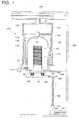
- FIG. 1is a cross-sectional view of heat treatment equipment in accordance with an embodiment
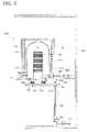
- FIG. 2is a cross-sectional view illustrating a flow path of gases, upon exhaust of the heat treatment equipment of FIG. 1 ;
- FIG. 3is a cross-sectional view of heat treatment equipment in accordance with another embodiment
- FIG. 4is an enlarged cross-sectional view of the “A” portion of FIG. 3 showing a check valve in an open state;
- FIG. 5is a cross-sectional view illustrating a check valve of FIG. 3 in a closed state
- FIG. 6is a cross-sectional view of heat treatment equipment in accordance with another embodiment of FIG. 1 .
- FIG. 1is a cross-sectional view of heat treatment equipment 100 in accordance with an embodiment of the present invention
- FIG. 2is a cross-sectional view illustrating a flow path of gases during exhaust of the heat treatment equipment 100 of FIG. 1 .
- the heat treatment equipment 100comprising vertical furnace equipment with a vertical-type process tube 110 , is installed inside a clean room 180 .
- the heat treatment equipment 100comprises the process tube 110 , a tube cap 150 , a movement unit 160 , a heater 120 , an exhaust duct 185 , a pressure control member 140 , and a control unit (not shown).
- the process tube 110provides a space for performing a heat treatment process on a wafer 90 and includes, at its one side, a wafer entrance/exit for wafers to enter and exit the process tube 110 .
- the tube cap 150seals the wafer entrance/exit of the process tube 110 .
- the movement unit 160moves the tube cap 150 during the process.
- the heater 120heats the process tube 110 .
- the exhaust duct 185exhausts gases present within the process tube 110 to the outside.
- the pressure control member 140is interposed between the process tube 110 and the exhaust duct 185 and maintains the pressure (P 1 ) inside the process tube 110 to be higher than the pressure (P 2 ) inside the clean room 180 , which is the pressure outside the process tube 110 .
- the control unit(not shown) generally controls the driving of the heat treatment equipment 100 .
- the process tube 110may be formed in the shape of a hollow cylinder so that a number of wafers 90 can fit inside.
- the process tube 110may be made of a quartz material that is suitable for the heat treatment process.
- the wafer entrance/exitis positioned at a lower part of the process tube 110 .
- the wafers 90are sequentially loaded in a wafer boat 170 in a vertically arrangement. Then, the wafers 90 in the wafer boat 170 enter the process tube 110 through the wafer entrance/exit.
- a gas exhaust bole 118is formed on the top of the process tube 110 .
- the gases present within the process tube 110are exhausted through the gas exhaust hole 118 .
- the gas exhaust hole 118may be operatively connected to the pressure control member 140 through a first gas exhaust line 183 which is a separate line, or it may be directly connected to the pressure control member 140 .
- a flange 112may be installed at the bottom of the process tube 110 .
- the flange 112is in contact with the process tube 110 to closely support the process tube 110 .
- the wafer entrance/exit for entering or exiting the wafers 90 into or from the process tube 110may be formed below the flange 112 , and the wafer boat 170 is supplied into the process tube 110 through the wafer entrance/exit formed at the flange 112 .
- a gas supply line 114is installed at one side of the flange 112 , to supply a predetermined ambient gas to the inside of the process tube 110 during the heat treatment process.
- the predetermined gasmay be nitrogen (N 2 ) gas.
- the gas supply line 114is installed at one side of the flange 112 in the present embodiment, but it may be directly installed at one side of the process tube 110 to supply the predetermined ambient gas to the inside of the process tube 110 .
- the tube cap 150is moved by the movement unit 160 and selectively seals the wafer entrance/exit of the process tube 110 .
- the process tube 110is sealed from the outside by the tube cap 150 .
- a seal ring 155such as an o-ring, may be placed on the tube cap 150 and be configured to come in contact with the process tube 110 . In this case, the possibility of a leak between the process tube 110 and the tube cap 150 is minimized.
- the tube cap 150seals the wafer entrance/exit formed at the flange 112 , thereby sealing the process tube 110 .
- the movement unit 160moves the tube cap 150 to seal the process tube 110 during the heat treatment process.
- the movement unit 160may be applied in various ways that are capable of moving the tube cap 150 a predetermined distance according to the control of the control unit. For example, a ball screw mode, cylinder mode, or linear motor mode may be applied as the movement unit 160 .
- the movement unit 160comprises a cap base 161 , a driving shaft 168 , bearings 165 and 166 , a base connector 163 , a motor 167 , and a power transmitter 164 .
- the cap base 161supports the tube cap 150 .
- the driving shaft 168is vertically installed under the process tube 110 and includes a male screw on its outer surface.
- the bearings 165 and 166are positioned at the upper and lower parts of the driving shaft 168 , respectively, so that the driving shaft 168 rotates.
- the base connector 163is installed about the driving shaft 168 so that the base connector 163 moves vertically according to the rotation direction of the driving shaft 168 .
- One side of the base connector 163is connected to the cap base 161 .
- the motor 167rotates in two directions at a predetermined speed, so that the base connector 163 moves vertically.
- the power transmitter 164transfers the rotation force of the motor 167 to the driving shaft 168 , so that the driving shaft 168 rotates by the rotation of the motor 167 .
- the control unitsends a predetermined signal to the motor 167 for rotation.
- the driving shaft 168then rotates at the predetermined speed by the power transferred from the power transmitter 164 , and the base connector 163 is vertically moved at the predetermined distance by the rotation of the driving shaft 168 .
- the cap base 161is vertically moved at the predetermined distance by the movement of the base connector 163
- the tube cap 150 positioned above the cap base 161is vertically moved at the predetermined distance by the vertical movement of the cap base 161 . Consequently, the process tube 110 is opened or closed by the movement of the tube cap 150 .
- the movement unit 160may further comprise an elastic member 162 to be installed between the tube cap 150 and the cap base 161 .
- an elastic member 162to be installed between the tube cap 150 and the cap base 161 .
- the holding force of the cap base 161 supporting the tube cap 150is absorbed by the elastic member 162 .
- the tube cap 150When the tube cap 150 seals the process tube 110 , the tube cap 150 gently comes into contact with the process tube 110 by the elastic force of the elastic member 162 and securely seals the process tube 110 .
- the heater 120is positioned outside the process tube 110 and heats the process tube 110 .
- the heater 120is capable of heating the process tube 110 at different temperature according to each heat treatment process performed inside the process tube 110 .
- the heater 120heats the process tube 110 to about 800° C. ⁇ 1200° C.
- the heater 120heats the process tube 110 to about 500° C. ⁇ 1000° C.
- the heater 120heats the process tube 110 to about 250° C. ⁇ 350° C.
- the heater 120may be applied in various modes which are capable of heating the process tube 110 .
- a coil heating mode, a lamp heating mode, or a peltier devicemay be applied as the heater 120 .
- the heater 120may be the coil heat mode.
- Another process chamber 130 enclosing the heater 120may be further installed outside the heater 120 . In this case, since the heat of the heater 120 heating the process tube 110 does not flow out to the outside by the process chamber 130 enclosing the heater 120 , the heating efficiency of the heater 120 is maximized.
- the exhaust duct 185is installed above the process chamber 130 and is connected to the process tube 110 by the pressure control member 140 .
- the gases present within the process chamber 130are discharged outside through the pressure control member 140 and the exhaust duct 185 . More specifically, one side of the exhaust duct 185 is connected to the pressure control member 140 , and the other side of the exhaust duct 185 is connected to a gas pumping unit (not shown).
- the gases present within the process tube 110are discharged outside through the pressure control member 140 and the exhaust duct 185 by the operation of the gas pumping unit.
- One side of the exhaust duct 185may be directly connected to the pressure control member 140 or may be connected to the pressure control member 140 by a second gas exhaust line 187 .
- the pressure control member 140maintains the pressure inside the process tube 110 to be higher than the pressure inside the clean room 180 where the heat treatment equipment 100 is installed, during the heat treatment process.
- the pressure control member 140is interposed between the process tube 110 and the exhaust duct 185 .
- the bottom of the pressure control member 140may be connected to the top of the process tube 110 by the first gas exhaust line 183 as described above, and the top of the pressure control member 140 may be connected to the bottom of the exhaust duct 185 by the second gas exhaust line 187 as described above.
- the bottom and top of the pressure control member 140may be directly connected to the process tube 110 and the exhaust duct 185 , respectively.
- the bottom of the pressure control member 140may be installed to be operatively connected to the gas exhaust hole 118 through which the gases present within the process tube 110 are exhausted, as described above.
- the pressure control member 140may be a hood directly connected to the process tube 110 .
- the pressure control member 140may be formed in the shape of a hollow cylinder.
- the first gas exhaust line 183 connected to the process tube 110may be connected to the lower side of the cylinder-shaped pressure control member 140
- the second gas exhaust line 187 connected to the exhaust duct 185may be connected to the upper side of the cylinder-shaped pressure control member 140 .
- One or more openings 143 being operatively connected to the clean room 180are formed at the pressure control member 140 .
- the gases present within the process tube 110are exhausted using the exhaust duct 185 and the pressure control member 140 connected to the exhaust duct 185 .
- the gases present outside the process tube 110i.e., the gases present inside the clean room 180 , may flow into the pressure control member 140 through the openings 143 .
- the gases present within the process tube 110are exhausted by the exhaust duct 185 and the pressure control member 140 connected to the exhaust duct 185 , not only the gases present within the process tube 110 but also the gases present outside the process tube 110 flow into the pressure control member 140 and are discharged to the exhaust duct 185 , through the openings 143 as a mixed gas.
- the openings 143may be formed at a side of the pressure control member 140 .
- the heat treatment equipment of the present inventionmay be realized in another embodiment illustrated in FIGS. 3 through 5 .
- FIG. 3is a cross-sectional view of heat treatment equipment in accordance with another embodiment
- FIG. 4is an enlarged cross-sectional view of the “A” portion of FIG. 3
- FIG. 5is a cross-sectional view illustrating a check valve 250 of FIG. 3 moved to a closed position.
- heat treatment equipment 200further comprises a check valve 250 in addition to the constituents of the heat treatment equipment 100 in accordance with the embodiment illustrated in FIGS. 1 and 2 .
- the check valve 250is installed in the opening 143 formed at the pressure control member 140 , and prevents the gas present within the pressure control member 140 from being discharged to the clean room 180 through the opening 143 .
- the check valve 250may be a normally opened valve that is opened only when the gas present within the pressure control member 140 is smoothly exhausted through the exhaust duct 185 but is closed otherwise.
- the check valve 250is installed at the opening 143 and comprises a valve housing 251 , a movement member 253 , and an elastic member 254 .
- the valve housing 251includes a gas flow path 252 .
- the movement member 253is installed inside the valve housing 251 and is reciprocally moved by a predetermined distance to open or close the gas flow path 252 .
- the elastic member 254is installed between the valve housing 251 and the movement 253 and allows the gas flow path 252 to be opened only when the gas present within the pressure control member 140 is smoothly exhausted.
- the valve housing 251may be formed in a tube shape.
- a pair of a first protrusion 256 and a second protrusion 257may be formed inside the valve housing 251 , spaced apart from each other at a predetermined interval, in a length direction of the valve housing 251 .
- the gas flow path 252may be formed between the first and second protrusions 256 and 257 .
- the first protrusion 256may be formed inside the valve housing 251 , at a position adjacent to the clean room 180
- the second protrusion 257may be formed inside the valve housing 251 , at a position adjacent to the inside of the pressure control member 140 .
- the movement member 253may be formed between the first and second protrusions 256 and 257 in the valve housing 251 .
- the movement member 253opens or closes the gas flow path 252 formed between the first and second protrusions 256 and 257 while reciprocally moving between the first and second protrusions 256 and 257 .
- the elastic member 254is positioned between the first protrusion 256 and the movement member 253 and pushes the movement member 253 toward the second protrusion 257 , with a predetermined elastic force. Without an applied external force, the movement member 253 is pushed toward the second protrusion 257 , as shown in FIG. 4 , by the elastic force of the elastic member 254 , and the gas flow path 252 is opened. As a result, the gas present outside the pressure control member 140 is able to flow into the pressure control member 140 through the gas flow path 252 of the check valve 250 positioned at the opening 143 .
- the gas pumping unit to exhaust the gases present within the pressure control member 140 and the exhaust duct 185is not working at full efficiency, the gas present within the pressure control member 140 and the exhaust duct 185 are not fully exhausted outside, and instead may flow backward into the pressure control member 140 .
- an external force caused by the back flow of the gasesacts on the movement member 253 as illustrated in FIG. 5 .
- the movement member 253is pushed toward the first protrusion 256 by the external force, and the gas flow path 252 of the check valve 250 is closed.
- the gas present within the pressure control member 140is not discharged outside through the opening 143 , due to the operation of the check valve 250 .
- the check valve 250may further comprise a seal ring 255 interposed between the first protrusion 256 and the movement member 253 . In this case, the closing of the gas flow path 252 by the external force becomes more effective by the seal ring 255 .
- FIG. 6Another embodiment of heat treatment equipment is illustrated in the cross-sectional view of FIG. 6 .
- heat treatment equipment 300comprises a process tube 110 , a gas supply line 114 , a tube cap 150 , a movement unit 160 , a heater 120 , a gas exhaust line 316 , a pump 380 , and a pressure control member 340 .
- the process tube 110provides a space for performing a heat treatment process on wafers 90 and includes, on its lower part, a wafer entrance/exit for supplying or exiting the wafers into or from the inside of the process tube 110 .
- the gas supply line 114supplies an ambient gas such as nitrogen (N 2 ) gas, in a certain amount, to the inside of the process tube 110 , thereby forming the ambient condition inside the process tube 110 .
- the tube cap 150seals the wafer entrance/exit of the process tube 110 .
- the movement unit 160moves the tube cap 150 during the process.
- the heater 120heats the process tube 110 .
- the gas exhaust line 316exhausts the gases present within the process tube 110 outside.
- the pump 380is positioned on the gas exhaust line 316 and pumps the gases present within the process tube 110 to the outside.
- the pressure control member 340is positioned on the gas exhaust line 316 and maintains the pressure inside the process tube 110 to be higher than the pressure inside the clean room 180 , which is the pressure outside the process tube 110 , during the process.
- the gas exhaust line 316may be formed at a side of the process tube 110 . Then the gases present within the process tube 110 may be exhausted to the outside, through the gas exhaust line 316 positioned at the side of the process tube 110 .
- the pressure control member 340is positioned on the gas exhaust line 316 but may be positioned in contact with the side of the process tube 110 .
- the pressure control member 340is formed in a hollow cylinder shape, and one or more openings 343 being operatively connected to the clean room 180 are formed at a side of the pressure control member 340 .
- the gas present within the process tube 110is exhausted by the gas exhaust line 316 and the pressure control member 340 connected to the gas exhaust line 316 , not only the gas present within the process tube 110 , which is supplied by the gas supply line 114 , but also the gas present outside the process tube 110 flow into the pressure control member 340 and are discharged to the gas exhaust line 316 as a mixed gas, through the openings 343 .
- the pressure inside the process tube 110is maintained higher than the pressure inside the clean room 180 , which is the pressure outside the process tube 110 .
- a user or a wafer transfer unit(not shown) first loads all wafers 90 in the wafer boat 170 positioned on the tube cap 150 .
- the movement unit 160then raises the tube cap 150 , so that the wafer boat 170 moves into the process tube 110 .
- the movement unit 160again raises the tube cap 150 by a predetermined distance. This last motion helps to securely seal the tube cap 150 against the process tube 110 .
- the desired ambient condition for the heat treatment processis created inside the process tube 110 .
- the heater 120 positioned outside the process tube 110heats the process tube 110 to perform the heat treatment process. That is, a predetermined ambient gas, such as nitrogen (N 2 ) gas, may be continuously supplied through the gas supply line 114 connected to the process tube 110 .
- the gas present within the process tube 110may be continuously exhausted to the outside through the exhaust duct 185 connected to the gas exhaust hole 118 of the process tube 110 , so that the predetermined ambient condition for the heat treatment process is formed inside the process tube 110 .
- the gas exhaust hole 118 formed in the process tube 110is not directly connected to the exhaust duct 185 . Instead, the gas exhaust hole 118 is connected to the exhaust duct 185 through the hollow pressure control member 140 with one or more openings 143 formed at its side. Upon exhausting the gases, the pressure control member 140 and the openings 143 automatically control the pressure inside the process tube 110 , so that the pressure (P 1 ) inside the process tube 110 is maintained as a positive pressure higher than the pressure (P 2 ) inside the clean room 180 .
- the hollow pressure control member 140 with one or more openings 143 formed at its sideis interposed between the exhaust duct 185 and the gas exhaust hole 118 of the process tube 110 .
- the gas present within the clean room 180automatically flows into the pressure control member 140 through the openings 143 and is then discharged to the outside through the exhaust duct 185 .
- the pressure (P 1 ) inside the process tube 110is continuously maintained to be higher than the pressure (P 2 ) inside the clean room 180 , which is the pressure outside the process tube 110 .
- any oxidants, such as O 2 or H 2 O, existing inside the clean room 180cannot flow into the process tube 110 due to the difference between the pressure (P 1 ) inside the process tube 110 and the pressure (P 2 ) inside the clean room 180 .
- the hollow-shaped pressure control member with one or more openings formed at its one sideis interposed between the exhaust duct and the gas exhaust hole of the process tube.
- the pressure inside the process tubeis continuously maintained higher than the pressure inside the clean room, which is the pressure outside the process tube.
Landscapes
- Engineering & Computer Science (AREA)
- Physics & Mathematics (AREA)
- Condensed Matter Physics & Semiconductors (AREA)
- General Physics & Mathematics (AREA)
- Manufacturing & Machinery (AREA)
- Computer Hardware Design (AREA)
- Microelectronics & Electronic Packaging (AREA)
- Power Engineering (AREA)
- Mechanical Engineering (AREA)
- General Engineering & Computer Science (AREA)
Abstract
Description
This application claims priority from Korean Patent Application No. 2006-65611, filed Jul. 13, 2006, the disclosure of which is hereby incorporated herein by reference in its entirety as if set forth fully herein.
1. Technical Field
The present invention relates to equipment used in a semiconductor device fabrication process, and more particularly, to heat treatment equipment for processing a substrate such as a wafer through a heat treatment process.
2. Discussion of the Related Art
Technology for semiconductor products continues to rapidly develop. Parameters of these semiconductor products, such as a processing speed and an amount of data stored per volume, have improved with the technology.
Generally, semiconductor products are manufactured by the following processes: a wafer fabrication process of fabricating a wafer using pure silicon, a FAB process of fabricating semiconductor chips on the manufactured wafer, an EDS process of testing and repairing the fabricated semiconductor chips, and a packaging process of packaging the tested and repaired semiconductor chips.
Among the aforementioned processes, the FAB process may include a number of unit processes such as an oxidation process of forming a silicon oxide layer on a wafer, a photoresist coating process of coating the wafer with photoresist as a photosensitive agent, an exposure process of exposing the coated wafer to a light having a predetermined wavelength so that a certain pattern is transmitted on the coated photoresist, a photoresist bake process of baking the coated photoresist, a development process of developing the exposed pattern on the wafer, an etching process of etching a part or the whole of a thin film formed on the wafer, a deposition process of depositing a predetermined thin film on the wafer, an ion-implantation process of implanting impurities in a specific layer on the wafer, an anneal process of activating the impurities, and a diffusion process of diffusing the impurities in silicon.
The EDS process includes a number of unit processes such as a pre-laser process of generating data by testing semiconductor chips within the wafer and distinguishing good or bad semiconductor chips, a laser-repair process of repairing the semiconductor chips to be repaired based on the generated data by using a laser beam, a post-laser process of testing the repaired semiconductor chips in the wafer, a back grinding process of polishing the rear side of the wafer, a protection layer coating process of coating the semiconductor chips in the wafer with a protection layer such as a polyimide layer, and a protection layer bake process of baking the protection layer such as the coated polyimide layer.
Among the aforementioned unit processes, the oxidation process, the photoresist bake process, the deposition process, the anneal process, the diffusion process, and the protection layer bake process are performed by a heat treatment process. The heat treatment equipment to perform the heat treatment process falls into two categories; a single wafer type and a batch type.
The batch type generally includes horizontal and vertical furnace equipment. The vertical furnace equipment in the batch type is generally used because it has many merits such as high productivity and reliability.
Among the unit processes performed by the heat treatment process, the protection layer bake process is performed after pads formed in the semiconductor chips are bonded to lead frames. And this is done before the packaging process of enclosing the pads with epoxy molding compound.
The protection layer bake process is generally performed by loading a number of wafers a sealed tube, and heating the tube to about 250° C.˜350° C. for about 2˜3 hours. During the protection layer bake process, nitrogen (N2) gas is continuously supplied into the tube as a process gas as a part of the ambient condition inside the tube.
Since various bad gases, including a silicon source out-gassing from the wafer, may be generated inside the tube during the protection layer bake process, the tube is typically connected to an exhaust duct positioned inside a clean room, so that the bad gases are continuously discharged to the outside.
However, in a conventional protection layer bake process, since the tube subjected to the bake process is directly connected to the exhaust duct, the gases present within the tube are rapidly discharged through the exhaust duct during the bake process. As a result, the pressure inside the tube is continuously maintained to be lower (hereinafter, referred to as “negative pressure”) than the pressure inside the clean room in which the heat treatment equipment is positioned.
Consequently, since the pressure inside the tube is maintained at a negative pressure while the protection layer bake process is performed, an oxidant, such as O2or H2O, present in the clean room flows into the tube due to the pressure difference between the clean room and the tube, even though the tube is sealed. As a result, the oxidant flowing into the inside of the tube interacts with the silicon source out-gassing from the wafers, causing an abnormal layer such as a silicon oxide layer (SiO2) to grow on the pads formed in the semiconductor chips on the wafers. Consequently, the abnormal layer, such as the silicon oxide layer formed on the pads, acts as an element to deteriorate the wire bonding which connects the pads to the lead frames, and this may cause a malfunction or performance deterioration of packaged semiconductor products.
Therefore, the present invention is directed to providing heat treatment equipment that prevents an abnormal layer from growing on pads formed in semiconductor chips on a wafer.
Another object of the present invention is to providing heat treatment equipment that prevents an oxidant existing inside a clean room from flowing into a process tube.
Exemplary embodiment provide heat treatment equipment comprising: a process tube; an exhaust duct connected to the process tube and exhausting gases present within the process tube; and a hollow pressure control member interposed between the process tube and the exhaust duct to be operatively connected to the process tube and the exhaust duct, and including one or more openings.
Preferably, the opening may include a check valve preventing a gas present within the pressure control member from discharging outside, through the opening.
Preferably, the process tube may include, at one side thereof, a gas exhaust hole through which gases present within the process tube are exhausted. In this case, the pressure control member may be installed in contact with the side of the process tube, to be operatively connected to the gas exhaust hole.
Preferably, the gas exhaust hole may be formed on the top side of the process tube. In this case, the pressure control member may be installed in contact with the top side of the process tube.
Preferably, the gas exhaust hole may be formed at one side of the process tube. In this case, the pressure control member may be installed in contact with the side of the process tube.
Preferably, the process tube may be operatively connected to the bottom of the pressure control member, and the exhaust duct may be operatively connected to the top of the pressure control member. In this case, the pressure control member may be formed in a cylinder shape, and the opening may be formed at a side of the pressure control member.
Preferably, the heat treatment equipment may further comprise a heater positioned outside the process tube and heating the process tube.
Other exemplary embodiments provide heat treatment equipment comprising: a process tube; an exhaust duct exhausting gases present within the process tube; a hollow pressure control member interposed between the process tube and the exhaust duct and including one or a number of openings; a first gas exhaust line connecting the process tube and the pressure control member to be operatively connected to each other; and a second gas exhaust line connecting the pressure control member and the exhaust duct to be operatively connected to each other.
Preferably, the opening may include a check valve preventing a gas present within the pressure control member from discharging outside through the opening.
Preferably, one end of the first gas exhaust line may be connected to the top side of the process tube, and the other end of the first gas exhaust line may be connected to the bottom side of the pressure control member.
Preferably, one end of the second gas exhaust line may be connected to the top side of the control pressure member, and the other end of the second gas exhaust line may be connected to the bottom side of the exhaust duct.
Preferably, the pressure control member may be formed in a cylinder shape. In this case, the opening may be formed at a side of the pressure control member.
Preferably, the heat treatment equipment may further comprise a heater positioned outside the process tube to heat the process tube.
The above and other features and advantages of the present invention will become more apparent to those of ordinary skill in the art by describing in detail preferred embodiments thereof with reference to the attached drawings in which:
The present invention will now be described more fully hereinafter with reference to the accompanying drawings, in which preferred embodiments of the invention are shown. This invention may, however, be embodied in many different forms and should not be construed as being limited to the embodiments set forth herein. Rather, these embodiments are provided so that this disclosure will be thorough and complete, and will fully convey the scope of the invention to those skilled in the art. Like numbers refer to like elements throughout the specification.
As illustrated inFIGS. 1 and 2 , theheat treatment equipment 100, comprising vertical furnace equipment with a vertical-type process tube 110, is installed inside aclean room 180.
More specifically, theheat treatment equipment 100 comprises theprocess tube 110, atube cap 150, amovement unit 160, aheater 120, anexhaust duct 185, apressure control member 140, and a control unit (not shown). Theprocess tube 110 provides a space for performing a heat treatment process on awafer 90 and includes, at its one side, a wafer entrance/exit for wafers to enter and exit theprocess tube 110. Thetube cap 150 seals the wafer entrance/exit of theprocess tube 110. Themovement unit 160 moves thetube cap 150 during the process. Theheater 120 heats theprocess tube 110. Theexhaust duct 185 exhausts gases present within theprocess tube 110 to the outside. Thepressure control member 140 is interposed between theprocess tube 110 and theexhaust duct 185 and maintains the pressure (P1) inside theprocess tube 110 to be higher than the pressure (P2) inside theclean room 180, which is the pressure outside theprocess tube 110. The control unit (not shown) generally controls the driving of theheat treatment equipment 100.
Theprocess tube 110 may be formed in the shape of a hollow cylinder so that a number ofwafers 90 can fit inside. Theprocess tube 110 may be made of a quartz material that is suitable for the heat treatment process. In the embodiment, the wafer entrance/exit is positioned at a lower part of theprocess tube 110. Thewafers 90 are sequentially loaded in awafer boat 170 in a vertically arrangement. Then, thewafers 90 in thewafer boat 170 enter theprocess tube 110 through the wafer entrance/exit.
Agas exhaust bole 118 is formed on the top of theprocess tube 110. The gases present within theprocess tube 110 are exhausted through thegas exhaust hole 118. Thegas exhaust hole 118 may be operatively connected to thepressure control member 140 through a firstgas exhaust line 183 which is a separate line, or it may be directly connected to thepressure control member 140.
Aflange 112 may be installed at the bottom of theprocess tube 110. Theflange 112 is in contact with theprocess tube 110 to closely support theprocess tube 110. In this case, the wafer entrance/exit for entering or exiting thewafers 90 into or from theprocess tube 110 may be formed below theflange 112, and thewafer boat 170 is supplied into theprocess tube 110 through the wafer entrance/exit formed at theflange 112. Agas supply line 114 is installed at one side of theflange 112, to supply a predetermined ambient gas to the inside of theprocess tube 110 during the heat treatment process. The predetermined gas may be nitrogen (N2) gas. Thegas supply line 114 is installed at one side of theflange 112 in the present embodiment, but it may be directly installed at one side of theprocess tube 110 to supply the predetermined ambient gas to the inside of theprocess tube 110.
Thetube cap 150 is moved by themovement unit 160 and selectively seals the wafer entrance/exit of theprocess tube 110. Here, theprocess tube 110 is sealed from the outside by thetube cap 150. Aseal ring 155, such as an o-ring, may be placed on thetube cap 150 and be configured to come in contact with theprocess tube 110. In this case, the possibility of a leak between theprocess tube 110 and thetube cap 150 is minimized. When theflange 112 closely supporting theprocess tube 110 is installed at the bottom of theprocess tube 110, thetube cap 150 seals the wafer entrance/exit formed at theflange 112, thereby sealing theprocess tube 110.
Themovement unit 160 moves thetube cap 150 to seal theprocess tube 110 during the heat treatment process. Themovement unit 160 may be applied in various ways that are capable of moving the tube cap150 a predetermined distance according to the control of the control unit. For example, a ball screw mode, cylinder mode, or linear motor mode may be applied as themovement unit 160.
As one example, themovement unit 160 comprises acap base 161, a drivingshaft 168,bearings base connector 163, amotor 167, and apower transmitter 164.
Thecap base 161 supports thetube cap 150. The drivingshaft 168 is vertically installed under theprocess tube 110 and includes a male screw on its outer surface. Thebearings shaft 168, respectively, so that the drivingshaft 168 rotates. Thebase connector 163 is installed about the drivingshaft 168 so that thebase connector 163 moves vertically according to the rotation direction of the drivingshaft 168. One side of thebase connector 163 is connected to thecap base 161.
Themotor 167 rotates in two directions at a predetermined speed, so that thebase connector 163 moves vertically. Thepower transmitter 164 transfers the rotation force of themotor 167 to the drivingshaft 168, so that the drivingshaft 168 rotates by the rotation of themotor 167.
When thetube cap 150 needs to be moved, the control unit sends a predetermined signal to themotor 167 for rotation. The drivingshaft 168 then rotates at the predetermined speed by the power transferred from thepower transmitter 164, and thebase connector 163 is vertically moved at the predetermined distance by the rotation of the drivingshaft 168. As a result, thecap base 161 is vertically moved at the predetermined distance by the movement of thebase connector 163, and thetube cap 150 positioned above thecap base 161 is vertically moved at the predetermined distance by the vertical movement of thecap base 161. Consequently, theprocess tube 110 is opened or closed by the movement of thetube cap 150.
Themovement unit 160 may further comprise anelastic member 162 to be installed between thetube cap 150 and thecap base 161. In this case, the holding force of thecap base 161 supporting thetube cap 150 is absorbed by theelastic member 162. When thetube cap 150 seals theprocess tube 110, thetube cap 150 gently comes into contact with theprocess tube 110 by the elastic force of theelastic member 162 and securely seals theprocess tube 110.
Theheater 120 is positioned outside theprocess tube 110 and heats theprocess tube 110. Theheater 120 is capable of heating theprocess tube 110 at different temperature according to each heat treatment process performed inside theprocess tube 110. For example, when the heat treatment process performed inside theprocess tube 110 is for the diffusion process, theheater 120 heats theprocess tube 110 to about 800° C.˜1200° C. For another example, when the heat treatment process performed inside theprocess tube 110 is for the deposition process, theheater 120 heats theprocess tube 110 to about 500° C.˜1000° C. For yet another example, when the process performed inside theprocess tube 110 is the protection layer bake process of baking the protection layer, such as a polyimide layer, coated on the semiconductor chips inside the wafers, theheater 120 heats theprocess tube 110 to about 250° C.˜350° C.
Theheater 120 may be applied in various modes which are capable of heating theprocess tube 110. For example, a coil heating mode, a lamp heating mode, or a peltier device may be applied as theheater 120. Preferably, theheater 120 may be the coil heat mode. Anotherprocess chamber 130 enclosing theheater 120 may be further installed outside theheater 120. In this case, since the heat of theheater 120 heating theprocess tube 110 does not flow out to the outside by theprocess chamber 130 enclosing theheater 120, the heating efficiency of theheater 120 is maximized.
In the embodiment, theexhaust duct 185 is installed above theprocess chamber 130 and is connected to theprocess tube 110 by thepressure control member 140. The gases present within theprocess chamber 130 are discharged outside through thepressure control member 140 and theexhaust duct 185. More specifically, one side of theexhaust duct 185 is connected to thepressure control member 140, and the other side of theexhaust duct 185 is connected to a gas pumping unit (not shown). The gases present within theprocess tube 110 are discharged outside through thepressure control member 140 and theexhaust duct 185 by the operation of the gas pumping unit. One side of theexhaust duct 185 may be directly connected to thepressure control member 140 or may be connected to thepressure control member 140 by a secondgas exhaust line 187.
Thepressure control member 140 maintains the pressure inside theprocess tube 110 to be higher than the pressure inside theclean room 180 where theheat treatment equipment 100 is installed, during the heat treatment process. Thepressure control member 140 is interposed between theprocess tube 110 and theexhaust duct 185.
As an example, the bottom of thepressure control member 140 may be connected to the top of theprocess tube 110 by the firstgas exhaust line 183 as described above, and the top of thepressure control member 140 may be connected to the bottom of theexhaust duct 185 by the secondgas exhaust line 187 as described above. However, as another example, the bottom and top of thepressure control member 140 may be directly connected to theprocess tube 110 and theexhaust duct 185, respectively. In this case, preferably, the bottom of thepressure control member 140 may be installed to be operatively connected to thegas exhaust hole 118 through which the gases present within theprocess tube 110 are exhausted, as described above. Thepressure control member 140 may be a hood directly connected to theprocess tube 110.
More specifically, thepressure control member 140 may be formed in the shape of a hollow cylinder. The firstgas exhaust line 183 connected to theprocess tube 110 may be connected to the lower side of the cylinder-shapedpressure control member 140, and the secondgas exhaust line 187 connected to theexhaust duct 185 may be connected to the upper side of the cylinder-shapedpressure control member 140.
One ormore openings 143 being operatively connected to theclean room 180 are formed at thepressure control member 140. The gases present within theprocess tube 110 are exhausted using theexhaust duct 185 and thepressure control member 140 connected to theexhaust duct 185. Upon exhaust, the gases present outside theprocess tube 110, i.e., the gases present inside theclean room 180, may flow into thepressure control member 140 through theopenings 143. That is, when the gases present within theprocess tube 110 are exhausted by theexhaust duct 185 and thepressure control member 140 connected to theexhaust duct 185, not only the gases present within theprocess tube 110 but also the gases present outside theprocess tube 110 flow into thepressure control member 140 and are discharged to theexhaust duct 185, through theopenings 143 as a mixed gas. Theopenings 143 may be formed at a side of thepressure control member 140.
The heat treatment equipment of the present invention may be realized in another embodiment illustrated inFIGS. 3 through 5 .
As illustrated inFIGS. 3 through 5 ,heat treatment equipment 200 further comprises acheck valve 250 in addition to the constituents of theheat treatment equipment 100 in accordance with the embodiment illustrated inFIGS. 1 and 2 . Thecheck valve 250 is installed in theopening 143 formed at thepressure control member 140, and prevents the gas present within thepressure control member 140 from being discharged to theclean room 180 through theopening 143. Thecheck valve 250 may be a normally opened valve that is opened only when the gas present within thepressure control member 140 is smoothly exhausted through theexhaust duct 185 but is closed otherwise.
More specifically, thecheck valve 250 is installed at theopening 143 and comprises avalve housing 251, amovement member 253, and anelastic member 254. Thevalve housing 251 includes agas flow path 252. Themovement member 253 is installed inside thevalve housing 251 and is reciprocally moved by a predetermined distance to open or close thegas flow path 252. Theelastic member 254 is installed between thevalve housing 251 and themovement 253 and allows thegas flow path 252 to be opened only when the gas present within thepressure control member 140 is smoothly exhausted.
Thevalve housing 251 may be formed in a tube shape. A pair of afirst protrusion 256 and asecond protrusion 257 may be formed inside thevalve housing 251, spaced apart from each other at a predetermined interval, in a length direction of thevalve housing 251. In this case, thegas flow path 252 may be formed between the first andsecond protrusions first protrusion 256 may be formed inside thevalve housing 251, at a position adjacent to theclean room 180, and thesecond protrusion 257 may be formed inside thevalve housing 251, at a position adjacent to the inside of thepressure control member 140.
Themovement member 253 may be formed between the first andsecond protrusions valve housing 251. Themovement member 253 opens or closes thegas flow path 252 formed between the first andsecond protrusions second protrusions
Theelastic member 254 is positioned between thefirst protrusion 256 and themovement member 253 and pushes themovement member 253 toward thesecond protrusion 257, with a predetermined elastic force. Without an applied external force, themovement member 253 is pushed toward thesecond protrusion 257, as shown inFIG. 4 , by the elastic force of theelastic member 254, and thegas flow path 252 is opened. As a result, the gas present outside thepressure control member 140 is able to flow into thepressure control member 140 through thegas flow path 252 of thecheck valve 250 positioned at theopening 143.
On the other hand, if the gas pumping unit to exhaust the gases present within thepressure control member 140 and theexhaust duct 185 is not working at full efficiency, the gas present within thepressure control member 140 and theexhaust duct 185 are not fully exhausted outside, and instead may flow backward into thepressure control member 140. In this case, an external force caused by the back flow of the gases acts on themovement member 253 as illustrated inFIG. 5 . Then, themovement member 253 is pushed toward thefirst protrusion 256 by the external force, and thegas flow path 252 of thecheck valve 250 is closed. As a result, the gas present within thepressure control member 140 is not discharged outside through theopening 143, due to the operation of thecheck valve 250.
Thecheck valve 250 may further comprise aseal ring 255 interposed between thefirst protrusion 256 and themovement member 253. In this case, the closing of thegas flow path 252 by the external force becomes more effective by theseal ring 255.
Another embodiment of heat treatment equipment is illustrated in the cross-sectional view ofFIG. 6 .
As illustrated inFIG. 6 ,heat treatment equipment 300 comprises aprocess tube 110, agas supply line 114, atube cap 150, amovement unit 160, aheater 120, agas exhaust line 316, apump 380, and apressure control member 340. Theprocess tube 110 provides a space for performing a heat treatment process onwafers 90 and includes, on its lower part, a wafer entrance/exit for supplying or exiting the wafers into or from the inside of theprocess tube 110. Thegas supply line 114 supplies an ambient gas such as nitrogen (N2) gas, in a certain amount, to the inside of theprocess tube 110, thereby forming the ambient condition inside theprocess tube 110. Thetube cap 150 seals the wafer entrance/exit of theprocess tube 110. Themovement unit 160 moves thetube cap 150 during the process. Theheater 120 heats theprocess tube 110. Thegas exhaust line 316 exhausts the gases present within theprocess tube 110 outside.
In this embodiment, thepump 380 is positioned on thegas exhaust line 316 and pumps the gases present within theprocess tube 110 to the outside. Thepressure control member 340 is positioned on thegas exhaust line 316 and maintains the pressure inside theprocess tube 110 to be higher than the pressure inside theclean room 180, which is the pressure outside theprocess tube 110, during the process.
Thegas exhaust line 316 may be formed at a side of theprocess tube 110. Then the gases present within theprocess tube 110 may be exhausted to the outside, through thegas exhaust line 316 positioned at the side of theprocess tube 110. Thepressure control member 340 is positioned on thegas exhaust line 316 but may be positioned in contact with the side of theprocess tube 110.
More specifically, thepressure control member 340 is formed in a hollow cylinder shape, and one ormore openings 343 being operatively connected to theclean room 180 are formed at a side of thepressure control member 340. When the gas present within theprocess tube 110 is exhausted by thegas exhaust line 316 and thepressure control member 340 connected to thegas exhaust line 316, not only the gas present within theprocess tube 110, which is supplied by thegas supply line 114, but also the gas present outside theprocess tube 110 flow into thepressure control member 340 and are discharged to thegas exhaust line 316 as a mixed gas, through theopenings 343. As a result, since the amount of gas being discharged to thegas exhaust line 316 is the same as or less than the amount of gas being supplied to the inside of theprocess tube 110 by thegas supply line 114, the pressure inside theprocess tube 110 is maintained higher than the pressure inside theclean room 180, which is the pressure outside theprocess tube 110.
A method of performing a heat treatment process using theheat treatment equipment 100 and effects thereof will be described in detail with reference to the embodiments ofFIGS. 1 and 2 .
A user or a wafer transfer unit (not shown) first loads allwafers 90 in thewafer boat 170 positioned on thetube cap 150. Themovement unit 160 then raises thetube cap 150, so that thewafer boat 170 moves into theprocess tube 110.
After thewafer boat 170 is moved into theprocess tube 110, themovement unit 160 again raises thetube cap 150 by a predetermined distance. This last motion helps to securely seal thetube cap 150 against theprocess tube 110.
After thetube cap 150 seals theprocess tube 110, the desired ambient condition for the heat treatment process is created inside theprocess tube 110. Theheater 120 positioned outside theprocess tube 110 heats theprocess tube 110 to perform the heat treatment process. That is, a predetermined ambient gas, such as nitrogen (N2) gas, may be continuously supplied through thegas supply line 114 connected to theprocess tube 110. The gas present within theprocess tube 110 may be continuously exhausted to the outside through theexhaust duct 185 connected to thegas exhaust hole 118 of theprocess tube 110, so that the predetermined ambient condition for the heat treatment process is formed inside theprocess tube 110.
During the heat treatment process, thegas exhaust hole 118 formed in theprocess tube 110 is not directly connected to theexhaust duct 185. Instead, thegas exhaust hole 118 is connected to theexhaust duct 185 through the hollowpressure control member 140 with one ormore openings 143 formed at its side. Upon exhausting the gases, thepressure control member 140 and theopenings 143 automatically control the pressure inside theprocess tube 110, so that the pressure (P1) inside theprocess tube 110 is maintained as a positive pressure higher than the pressure (P2) inside theclean room 180. Consequently, since the pressure (P1) inside theprocess tube 110 is maintained as the positive pressure, an oxidant, such as O2or H2O existing inside theclean room 180, cannot flow into theprocess tube 110 due to the pressure difference between the inside of theprocess tube 110 and the inside of theclean room 180. As a result, the embodiments of the present invention prevent all problems caused by an inflow of oxidants as are possible in the conventional art.
To the contrary, if thepressure control member 140 was not interposed between theexhaust duct 185 and thegas exhaust hole 118 of theprocess tube 110, as in conventional heat treatment equipment, but instead theexhaust duct 185 was directly connected to thegas exhaust hole 118 of theprocess tube 110, and when the amount of gas being discharged is greater than the amount of gas being supplied, the pressure (P1) inside theprocess tube 110 becomes lower than the pressure (P2) inside theclean room 180. This happens because, as mentioned above, the amount of the discharged gas is greater than the amount of the supplied gas. As a result, any oxidants existing outside theprocess tube 110 can flow into theprocess tube 110, thereby forming an abnormal layer on the wafers. This causes many problems such as wire bonding failure.
In the embodiments illustrated here, however, the hollowpressure control member 140 with one ormore openings 143 formed at its side is interposed between theexhaust duct 185 and thegas exhaust hole 118 of theprocess tube 110. Thus, upon exhaust, if the amount of gas being discharged is greater than the amount of gas being supplied, no longer does the difference between the amount of the discharged gas and the amount of the supplied gas matter. Instead, the gas present within theclean room 180 automatically flows into thepressure control member 140 through theopenings 143 and is then discharged to the outside through theexhaust duct 185. As a result, since the amount of the gas being exhausted through theexhaust duct 185 is the same as or less than the amount of the gas being supplied into theprocess tube 110, the pressure (P1) inside theprocess tube 110 is continuously maintained to be higher than the pressure (P2) inside theclean room 180, which is the pressure outside theprocess tube 110.
Thus, using theheat treatment equipment 100 in accordance with the embodiments presented here, since the pressure (P1) inside theprocess tube 110 is maintained as the positive pressure during the heat treatment process, any oxidants, such as O2or H2O, existing inside theclean room 180 cannot flow into theprocess tube 110 due to the difference between the pressure (P1) inside theprocess tube 110 and the pressure (P2) inside theclean room 180.
As described above, in accordance with the embodiments of the heat treatment equipment presented here, the hollow-shaped pressure control member with one or more openings formed at its one side is interposed between the exhaust duct and the gas exhaust hole of the process tube. As a result, when gas is exhausted for the heat treatment process, if the amount of gas being discharged is greater than the amount of gas being supplied, this difference no longer matters because the gas present within the clean room can automatically flow into the pressure control member through the openings of the pressure control member, and is ultimately discharged to the outside through the exhaust duct. Consequently, since the amount of the gas discharged to the exhaust duct is the same as or less than the amount of the gas supplied to the inside of the process tube, the pressure inside the process tube is continuously maintained higher than the pressure inside the clean room, which is the pressure outside the process tube.
The present invention has been described in reference to the embodiments illustrated in the drawings. However, it is to be understood that the scope of the invention is not limited to the disclosed embodiments. On the contrary, the scope of the invention is intended to include various modifications and alternative arrangements within the capabilities of persons skilled in the art using presently known or future technologies and equivalents. The scope of the claims, therefore, should be accorded the broadest interpretation so as to encompass all such modifications and similar arrangements.
Claims (18)
1. Heat treatment equipment comprising:
a process tube having an enclosed process space;
an exhaust duct connected to the process tube to exhaust gases present within the process tube; and
a hollow pressure control member interposed between the process tube and the exhaust duct, the pressure control member being operatively connected, via first openings, to the process tube and the exhaust duct respectively, and including one or more second openings to a part external to the process space,
wherein the process tube comprises a gas exhaust hole through which the gases present within the process tube are exhausted and the pressure control member is in physical contact with a side of the process tube so that the pressure control member is operatively connected to the gas exhaust hole.
2. The heat treatment equipment according toclaim 1 , wherein the one or more second openings comprise a check valve to prevent a gas present within the pressure control member from being discharged through the one or more second openings.
3. The heat treatment equipment according toclaim 1 , wherein the gas exhaust hole is formed in a top side of the process tube, and the pressure control member is in physical contact with the top side of the process tube.
4. The heat treatment equipment according toclaim 1 , wherein the gas exhaust hole is formed in a side of the process tube, and the pressure control member is in physical contact with the side of the process tube.
5. The heat treatment equipment according toclaim 1 , wherein the process tube is operatively connected to the bottom of the pressure control member, the exhaust duct is operatively connected to the top of the pressure control member, and the one or more second openings is formed at a side of the pressure control member.
6. The heat treatment equipment according toclaim 5 , wherein the pressure control member is the shape of a hollow cylinder.
7. The heat treatment equipment according toclaim 1 , further comprising a heater positioned outside the process tube to heat the process tube.
8. Heat treatment equipment comprising:
a process tube having an enclosed process space;
an exhaust duct for exhausting gases present in the process tube;
a hollow pressure control member interposed between the process tube and the exhaust duct and including one or more openings to a part external to the process space;
a first gas exhaust line enabling the process tube and the pressure control member to be operatively connected to each other via a first opening other than the one or more openings; and
a second gas exhaust line enabling the pressure control member and the exhaust duct to be operatively connected to each other via a second opening other than the one or more openings,
wherein the one or more openings comprise a check valve to prevent a gas present within the pressure control member from being discharged to outside through the opening.
9. The heat treatment equipment according toclaim 8 , wherein one end of the first gas exhaust line is connected to a top side of the process tube, and the other end of the first gas exhaust line is connected to a bottom side of the pressure control member.
10. The heat treatment equipment according toclaim 9 , wherein one end of the second gas exhaust line is connected to a top side of the pressure control member, and the other end of the second gas exhaust line is connected to a bottom side of the exhaust duct.
11. The heat treatment equipment according toclaim 8 , further comprising a heater outside the process tube to heat the process tube.
12. The heat treatment equipment according toclaim 8 , wherein the part external to the process space is a clean room.
13. Heat treatment equipment comprising:
a process tube having an enclosed process space;
an exhaust duct for exhausting gases present in the process tube;
a hollow pressure control member interposed between the process tube and the exhaust duct and including one or more openings to a part external to the process space;
a first gas exhaust line enabling the process tube and the pressure control member to be operatively connected to each other via a first opening other than the one or more openings; and
a second gas exhaust line enabling the pressure control member and the exhaust duct to be operatively connected to each other via a second opening other than the one or more openings,
wherein one end of the first gas exhaust line is connected to a top side of the process tube, and the other end of the first gas exhaust line is connected to a bottom side of the pressure control member,
wherein one end of the second gas exhaust line is connected to a top side of the pressure control member, and the other end of the second gas exhaust line is connected to a bottom side of the exhaust duct, and
wherein the pressure control member is cylindrical, and the one or more openings are formed on a side of the pressure control member.
14. Heat treatment equipment comprising:
a process tube having an enclosed process space;
an exhaust duct for exhausting gases present in the process tube;
a hollow pressure control member interposed between the process tube and the exhaust duct and including one or more openings to a part external to the process space;
a first gas exhaust line enabling the process tube and the pressure control member to be operatively connected to each other via a first opening other than the one or more openings;
a second gas exhaust line enabling the pressure control member and the exhaust duct to be operatively connected to each other via a second opening other than the one or more openings; and
a tube cap to hold objects to be heat treated and to seal the process tube, the tube cap operable to move to and from the process chamber.
15. A method of a heat treatment in a chamber, the method comprising:
providing a process gas at a first pressure in the chamber;
exhausting the gas into a pressure control chamber;
allowing an ambient gas external to the chamber, at a second pressure less than the first pressure, to enter the pressure control chamber;
forming a mixed gas that includes the process gas and the ambient gas; and
exhausting the mixed gas to outside the pressure control chamber.
16. The method ofclaim 15 , further comprising:
placing semiconductor wafers to be heat treated onto a tube cap; and
raising the tube cap to load the wafers into the chamber until the tube cap contacts a bottom portion of the chamber so that the tube cap creates a gas-tight seal with the chamber.
17. The method ofclaim 15 , further comprising controlling a flow of the ambient gas entering the pressure control chamber by using check valves.
18. The method ofclaim 15 , the method further comprising:
supplying the ambient gas from a clean room, and
providing an entrance path of the ambient gas through openings formed within the pressure control chamber.
Applications Claiming Priority (3)
| Application Number | Priority Date | Filing Date | Title |
|---|---|---|---|
| KR10-2006-0065611 | 2006-07-13 | ||
| KR1020060065611AKR100782484B1 (en) | 2006-07-13 | 2006-07-13 | Heat treatment equipment |
| KR2006-65611 | 2006-07-13 |
Publications (2)
| Publication Number | Publication Date |
|---|---|
| US20080011735A1 US20080011735A1 (en) | 2008-01-17 |
| US7850449B2true US7850449B2 (en) | 2010-12-14 |
Family
ID=38948203
Family Applications (1)
| Application Number | Title | Priority Date | Filing Date |
|---|---|---|---|
| US11/775,640Expired - Fee RelatedUS7850449B2 (en) | 2006-07-13 | 2007-07-10 | Heat treatment equipment |
Country Status (2)
| Country | Link |
|---|---|
| US (1) | US7850449B2 (en) |
| KR (1) | KR100782484B1 (en) |
Cited By (353)
| Publication number | Priority date | Publication date | Assignee | Title |
|---|---|---|---|---|
| US20130014896A1 (en)* | 2011-07-15 | 2013-01-17 | Asm Japan K.K. | Wafer-Supporting Device and Method for Producing Same |
| US10023960B2 (en) | 2012-09-12 | 2018-07-17 | Asm Ip Holdings B.V. | Process gas management for an inductively-coupled plasma deposition reactor |
| US10083836B2 (en) | 2015-07-24 | 2018-09-25 | Asm Ip Holding B.V. | Formation of boron-doped titanium metal films with high work function |
| US10134757B2 (en) | 2016-11-07 | 2018-11-20 | Asm Ip Holding B.V. | Method of processing a substrate and a device manufactured by using the method |
| US10229833B2 (en) | 2016-11-01 | 2019-03-12 | Asm Ip Holding B.V. | Methods for forming a transition metal nitride film on a substrate by atomic layer deposition and related semiconductor device structures |
| US10236177B1 (en) | 2017-08-22 | 2019-03-19 | ASM IP Holding B.V.. | Methods for depositing a doped germanium tin semiconductor and related semiconductor device structures |
| US10249524B2 (en) | 2017-08-09 | 2019-04-02 | Asm Ip Holding B.V. | Cassette holder assembly for a substrate cassette and holding member for use in such assembly |
| US10249577B2 (en) | 2016-05-17 | 2019-04-02 | Asm Ip Holding B.V. | Method of forming metal interconnection and method of fabricating semiconductor apparatus using the method |
| US10262859B2 (en) | 2016-03-24 | 2019-04-16 | Asm Ip Holding B.V. | Process for forming a film on a substrate using multi-port injection assemblies |
| US10269558B2 (en) | 2016-12-22 | 2019-04-23 | Asm Ip Holding B.V. | Method of forming a structure on a substrate |
| US10276355B2 (en) | 2015-03-12 | 2019-04-30 | Asm Ip Holding B.V. | Multi-zone reactor, system including the reactor, and method of using the same |
| US10283353B2 (en) | 2017-03-29 | 2019-05-07 | Asm Ip Holding B.V. | Method of reforming insulating film deposited on substrate with recess pattern |
| US10290508B1 (en) | 2017-12-05 | 2019-05-14 | Asm Ip Holding B.V. | Method for forming vertical spacers for spacer-defined patterning |
| US10312055B2 (en) | 2017-07-26 | 2019-06-04 | Asm Ip Holding B.V. | Method of depositing film by PEALD using negative bias |
| US10312129B2 (en) | 2015-09-29 | 2019-06-04 | Asm Ip Holding B.V. | Variable adjustment for precise matching of multiple chamber cavity housings |
| US10319588B2 (en) | 2017-10-10 | 2019-06-11 | Asm Ip Holding B.V. | Method for depositing a metal chalcogenide on a substrate by cyclical deposition |
| US10322384B2 (en) | 2015-11-09 | 2019-06-18 | Asm Ip Holding B.V. | Counter flow mixer for process chamber |
| US10340135B2 (en) | 2016-11-28 | 2019-07-02 | Asm Ip Holding B.V. | Method of topologically restricted plasma-enhanced cyclic deposition of silicon or metal nitride |
| US10340125B2 (en) | 2013-03-08 | 2019-07-02 | Asm Ip Holding B.V. | Pulsed remote plasma method and system |
| US10343920B2 (en) | 2016-03-18 | 2019-07-09 | Asm Ip Holding B.V. | Aligned carbon nanotubes |
| US10361201B2 (en) | 2013-09-27 | 2019-07-23 | Asm Ip Holding B.V. | Semiconductor structure and device formed using selective epitaxial process |
| US10364496B2 (en) | 2011-06-27 | 2019-07-30 | Asm Ip Holding B.V. | Dual section module having shared and unshared mass flow controllers |
| US10366864B2 (en) | 2013-03-08 | 2019-07-30 | Asm Ip Holding B.V. | Method and system for in-situ formation of intermediate reactive species |
| US10367080B2 (en) | 2016-05-02 | 2019-07-30 | Asm Ip Holding B.V. | Method of forming a germanium oxynitride film |
| US10381226B2 (en) | 2016-07-27 | 2019-08-13 | Asm Ip Holding B.V. | Method of processing substrate |
| US10381219B1 (en) | 2018-10-25 | 2019-08-13 | Asm Ip Holding B.V. | Methods for forming a silicon nitride film |
| US10378106B2 (en) | 2008-11-14 | 2019-08-13 | Asm Ip Holding B.V. | Method of forming insulation film by modified PEALD |
| US10388513B1 (en) | 2018-07-03 | 2019-08-20 | Asm Ip Holding B.V. | Method for depositing silicon-free carbon-containing film as gap-fill layer by pulse plasma-assisted deposition |
| US10388509B2 (en) | 2016-06-28 | 2019-08-20 | Asm Ip Holding B.V. | Formation of epitaxial layers via dislocation filtering |
| US10395919B2 (en) | 2016-07-28 | 2019-08-27 | Asm Ip Holding B.V. | Method and apparatus for filling a gap |
| US10403504B2 (en) | 2017-10-05 | 2019-09-03 | Asm Ip Holding B.V. | Method for selectively depositing a metallic film on a substrate |
| US10410943B2 (en) | 2016-10-13 | 2019-09-10 | Asm Ip Holding B.V. | Method for passivating a surface of a semiconductor and related systems |
| US10435790B2 (en) | 2016-11-01 | 2019-10-08 | Asm Ip Holding B.V. | Method of subatmospheric plasma-enhanced ALD using capacitively coupled electrodes with narrow gap |
| US10438965B2 (en) | 2014-12-22 | 2019-10-08 | Asm Ip Holding B.V. | Semiconductor device and manufacturing method thereof |
| US10446393B2 (en) | 2017-05-08 | 2019-10-15 | Asm Ip Holding B.V. | Methods for forming silicon-containing epitaxial layers and related semiconductor device structures |
| US10458018B2 (en) | 2015-06-26 | 2019-10-29 | Asm Ip Holding B.V. | Structures including metal carbide material, devices including the structures, and methods of forming same |
| US10468261B2 (en) | 2017-02-15 | 2019-11-05 | Asm Ip Holding B.V. | Methods for forming a metallic film on a substrate by cyclical deposition and related semiconductor device structures |
| US10468251B2 (en) | 2016-02-19 | 2019-11-05 | Asm Ip Holding B.V. | Method for forming spacers using silicon nitride film for spacer-defined multiple patterning |
| US10483099B1 (en) | 2018-07-26 | 2019-11-19 | Asm Ip Holding B.V. | Method for forming thermally stable organosilicon polymer film |
| US10480072B2 (en) | 2009-04-06 | 2019-11-19 | Asm Ip Holding B.V. | Semiconductor processing reactor and components thereof |
| US10501866B2 (en) | 2016-03-09 | 2019-12-10 | Asm Ip Holding B.V. | Gas distribution apparatus for improved film uniformity in an epitaxial system |
| US10504742B2 (en) | 2017-05-31 | 2019-12-10 | Asm Ip Holding B.V. | Method of atomic layer etching using hydrogen plasma |
| US10510536B2 (en) | 2018-03-29 | 2019-12-17 | Asm Ip Holding B.V. | Method of depositing a co-doped polysilicon film on a surface of a substrate within a reaction chamber |
| US10529563B2 (en) | 2017-03-29 | 2020-01-07 | Asm Ip Holdings B.V. | Method for forming doped metal oxide films on a substrate by cyclical deposition and related semiconductor device structures |
| US10529554B2 (en) | 2016-02-19 | 2020-01-07 | Asm Ip Holding B.V. | Method for forming silicon nitride film selectively on sidewalls or flat surfaces of trenches |
| US10529542B2 (en) | 2015-03-11 | 2020-01-07 | Asm Ip Holdings B.V. | Cross-flow reactor and method |
| US10535516B2 (en) | 2018-02-01 | 2020-01-14 | Asm Ip Holdings B.V. | Method for depositing a semiconductor structure on a surface of a substrate and related semiconductor structures |
| US10541333B2 (en) | 2017-07-19 | 2020-01-21 | Asm Ip Holding B.V. | Method for depositing a group IV semiconductor and related semiconductor device structures |
| US10541173B2 (en) | 2016-07-08 | 2020-01-21 | Asm Ip Holding B.V. | Selective deposition method to form air gaps |
| US10559458B1 (en) | 2018-11-26 | 2020-02-11 | Asm Ip Holding B.V. | Method of forming oxynitride film |
| US10561975B2 (en) | 2014-10-07 | 2020-02-18 | Asm Ip Holdings B.V. | Variable conductance gas distribution apparatus and method |
| US10566223B2 (en) | 2012-08-28 | 2020-02-18 | Asm Ip Holdings B.V. | Systems and methods for dynamic semiconductor process scheduling |
| US10590535B2 (en) | 2017-07-26 | 2020-03-17 | Asm Ip Holdings B.V. | Chemical treatment, deposition and/or infiltration apparatus and method for using the same |
| US10600673B2 (en) | 2015-07-07 | 2020-03-24 | Asm Ip Holding B.V. | Magnetic susceptor to baseplate seal |
| US10605530B2 (en) | 2017-07-26 | 2020-03-31 | Asm Ip Holding B.V. | Assembly of a liner and a flange for a vertical furnace as well as the liner and the vertical furnace |
| US10607895B2 (en) | 2017-09-18 | 2020-03-31 | Asm Ip Holdings B.V. | Method for forming a semiconductor device structure comprising a gate fill metal |
| US10604847B2 (en) | 2014-03-18 | 2020-03-31 | Asm Ip Holding B.V. | Gas distribution system, reactor including the system, and methods of using the same |
| USD880437S1 (en) | 2018-02-01 | 2020-04-07 | Asm Ip Holding B.V. | Gas supply plate for semiconductor manufacturing apparatus |
| US10612137B2 (en) | 2016-07-08 | 2020-04-07 | Asm Ip Holdings B.V. | Organic reactants for atomic layer deposition |
| US10612136B2 (en) | 2018-06-29 | 2020-04-07 | ASM IP Holding, B.V. | Temperature-controlled flange and reactor system including same |
| US10643904B2 (en) | 2016-11-01 | 2020-05-05 | Asm Ip Holdings B.V. | Methods for forming a semiconductor device and related semiconductor device structures |
| US10643826B2 (en) | 2016-10-26 | 2020-05-05 | Asm Ip Holdings B.V. | Methods for thermally calibrating reaction chambers |
| US10658205B2 (en) | 2017-09-28 | 2020-05-19 | Asm Ip Holdings B.V. | Chemical dispensing apparatus and methods for dispensing a chemical to a reaction chamber |
| US10658181B2 (en) | 2018-02-20 | 2020-05-19 | Asm Ip Holding B.V. | Method of spacer-defined direct patterning in semiconductor fabrication |
| US10655221B2 (en) | 2017-02-09 | 2020-05-19 | Asm Ip Holding B.V. | Method for depositing oxide film by thermal ALD and PEALD |
| US10665452B2 (en) | 2016-05-02 | 2020-05-26 | Asm Ip Holdings B.V. | Source/drain performance through conformal solid state doping |
| US10685834B2 (en) | 2017-07-05 | 2020-06-16 | Asm Ip Holdings B.V. | Methods for forming a silicon germanium tin layer and related semiconductor device structures |
| US10683571B2 (en) | 2014-02-25 | 2020-06-16 | Asm Ip Holding B.V. | Gas supply manifold and method of supplying gases to chamber using same |
| US10692741B2 (en) | 2017-08-08 | 2020-06-23 | Asm Ip Holdings B.V. | Radiation shield |
| US10707106B2 (en) | 2011-06-06 | 2020-07-07 | Asm Ip Holding B.V. | High-throughput semiconductor-processing apparatus equipped with multiple dual-chamber modules |
| US10714350B2 (en) | 2016-11-01 | 2020-07-14 | ASM IP Holdings, B.V. | Methods for forming a transition metal niobium nitride film on a substrate by atomic layer deposition and related semiconductor device structures |
| US10714335B2 (en) | 2017-04-25 | 2020-07-14 | Asm Ip Holding B.V. | Method of depositing thin film and method of manufacturing semiconductor device |
| US10714385B2 (en) | 2016-07-19 | 2020-07-14 | Asm Ip Holding B.V. | Selective deposition of tungsten |
| US10714315B2 (en) | 2012-10-12 | 2020-07-14 | Asm Ip Holdings B.V. | Semiconductor reaction chamber showerhead |
| US10731249B2 (en) | 2018-02-15 | 2020-08-04 | Asm Ip Holding B.V. | Method of forming a transition metal containing film on a substrate by a cyclical deposition process, a method for supplying a transition metal halide compound to a reaction chamber, and related vapor deposition apparatus |
| US10734244B2 (en) | 2017-11-16 | 2020-08-04 | Asm Ip Holding B.V. | Method of processing a substrate and a device manufactured by the same |
| US10734497B2 (en) | 2017-07-18 | 2020-08-04 | Asm Ip Holding B.V. | Methods for forming a semiconductor device structure and related semiconductor device structures |
| US10741385B2 (en) | 2016-07-28 | 2020-08-11 | Asm Ip Holding B.V. | Method and apparatus for filling a gap |
| US10755922B2 (en) | 2018-07-03 | 2020-08-25 | Asm Ip Holding B.V. | Method for depositing silicon-free carbon-containing film as gap-fill layer by pulse plasma-assisted deposition |
| US10767789B2 (en) | 2018-07-16 | 2020-09-08 | Asm Ip Holding B.V. | Diaphragm valves, valve components, and methods for forming valve components |
| US10770286B2 (en) | 2017-05-08 | 2020-09-08 | Asm Ip Holdings B.V. | Methods for selectively forming a silicon nitride film on a substrate and related semiconductor device structures |
| US10770336B2 (en) | 2017-08-08 | 2020-09-08 | Asm Ip Holding B.V. | Substrate lift mechanism and reactor including same |
| US10787741B2 (en) | 2014-08-21 | 2020-09-29 | Asm Ip Holding B.V. | Method and system for in situ formation of gas-phase compounds |
| US10797133B2 (en) | 2018-06-21 | 2020-10-06 | Asm Ip Holding B.V. | Method for depositing a phosphorus doped silicon arsenide film and related semiconductor device structures |
| US10804098B2 (en) | 2009-08-14 | 2020-10-13 | Asm Ip Holding B.V. | Systems and methods for thin-film deposition of metal oxides using excited nitrogen-oxygen species |
| US10811256B2 (en) | 2018-10-16 | 2020-10-20 | Asm Ip Holding B.V. | Method for etching a carbon-containing feature |
| US10818758B2 (en) | 2018-11-16 | 2020-10-27 | Asm Ip Holding B.V. | Methods for forming a metal silicate film on a substrate in a reaction chamber and related semiconductor device structures |
| USD900036S1 (en) | 2017-08-24 | 2020-10-27 | Asm Ip Holding B.V. | Heater electrical connector and adapter |
| US10832903B2 (en) | 2011-10-28 | 2020-11-10 | Asm Ip Holding B.V. | Process feed management for semiconductor substrate processing |
| US10829852B2 (en) | 2018-08-16 | 2020-11-10 | Asm Ip Holding B.V. | Gas distribution device for a wafer processing apparatus |
| US10847366B2 (en) | 2018-11-16 | 2020-11-24 | Asm Ip Holding B.V. | Methods for depositing a transition metal chalcogenide film on a substrate by a cyclical deposition process |
| US10844484B2 (en) | 2017-09-22 | 2020-11-24 | Asm Ip Holding B.V. | Apparatus for dispensing a vapor phase reactant to a reaction chamber and related methods |
| US10847371B2 (en) | 2018-03-27 | 2020-11-24 | Asm Ip Holding B.V. | Method of forming an electrode on a substrate and a semiconductor device structure including an electrode |
| US10847365B2 (en) | 2018-10-11 | 2020-11-24 | Asm Ip Holding B.V. | Method of forming conformal silicon carbide film by cyclic CVD |
| US10851456B2 (en) | 2016-04-21 | 2020-12-01 | Asm Ip Holding B.V. | Deposition of metal borides |
| USD903477S1 (en) | 2018-01-24 | 2020-12-01 | Asm Ip Holdings B.V. | Metal clamp |
| US10858737B2 (en) | 2014-07-28 | 2020-12-08 | Asm Ip Holding B.V. | Showerhead assembly and components thereof |
| US10865475B2 (en) | 2016-04-21 | 2020-12-15 | Asm Ip Holding B.V. | Deposition of metal borides and silicides |
| US10867786B2 (en) | 2018-03-30 | 2020-12-15 | Asm Ip Holding B.V. | Substrate processing method |
| US10867788B2 (en) | 2016-12-28 | 2020-12-15 | Asm Ip Holding B.V. | Method of forming a structure on a substrate |
| US10872771B2 (en) | 2018-01-16 | 2020-12-22 | Asm Ip Holding B. V. | Method for depositing a material film on a substrate within a reaction chamber by a cyclical deposition process and related device structures |
| US10886123B2 (en) | 2017-06-02 | 2021-01-05 | Asm Ip Holding B.V. | Methods for forming low temperature semiconductor layers and related semiconductor device structures |
| US10883175B2 (en) | 2018-08-09 | 2021-01-05 | Asm Ip Holding B.V. | Vertical furnace for processing substrates and a liner for use therein |
| US10892156B2 (en) | 2017-05-08 | 2021-01-12 | Asm Ip Holding B.V. | Methods for forming a silicon nitride film on a substrate and related semiconductor device structures |
| US10896820B2 (en) | 2018-02-14 | 2021-01-19 | Asm Ip Holding B.V. | Method for depositing a ruthenium-containing film on a substrate by a cyclical deposition process |
| US10910262B2 (en) | 2017-11-16 | 2021-02-02 | Asm Ip Holding B.V. | Method of selectively depositing a capping layer structure on a semiconductor device structure |
| US10914004B2 (en) | 2018-06-29 | 2021-02-09 | Asm Ip Holding B.V. | Thin-film deposition method and manufacturing method of semiconductor device |
| US10923344B2 (en) | 2017-10-30 | 2021-02-16 | Asm Ip Holding B.V. | Methods for forming a semiconductor structure and related semiconductor structures |
| US10928731B2 (en) | 2017-09-21 | 2021-02-23 | Asm Ip Holding B.V. | Method of sequential infiltration synthesis treatment of infiltrateable material and structures and devices formed using same |
| US10934619B2 (en) | 2016-11-15 | 2021-03-02 | Asm Ip Holding B.V. | Gas supply unit and substrate processing apparatus including the gas supply unit |
| US10941490B2 (en) | 2014-10-07 | 2021-03-09 | Asm Ip Holding B.V. | Multiple temperature range susceptor, assembly, reactor and system including the susceptor, and methods of using the same |
| US10975470B2 (en) | 2018-02-23 | 2021-04-13 | Asm Ip Holding B.V. | Apparatus for detecting or monitoring for a chemical precursor in a high temperature environment |
| US11001925B2 (en) | 2016-12-19 | 2021-05-11 | Asm Ip Holding B.V. | Substrate processing apparatus |
| US11015245B2 (en) | 2014-03-19 | 2021-05-25 | Asm Ip Holding B.V. | Gas-phase reactor and system having exhaust plenum and components thereof |
| US11018002B2 (en) | 2017-07-19 | 2021-05-25 | Asm Ip Holding B.V. | Method for selectively depositing a Group IV semiconductor and related semiconductor device structures |
| US11018047B2 (en) | 2018-01-25 | 2021-05-25 | Asm Ip Holding B.V. | Hybrid lift pin |
| US11024523B2 (en) | 2018-09-11 | 2021-06-01 | Asm Ip Holding B.V. | Substrate processing apparatus and method |
| US11022879B2 (en) | 2017-11-24 | 2021-06-01 | Asm Ip Holding B.V. | Method of forming an enhanced unexposed photoresist layer |
| US11031242B2 (en) | 2018-11-07 | 2021-06-08 | Asm Ip Holding B.V. | Methods for depositing a boron doped silicon germanium film |
| USD922229S1 (en) | 2019-06-05 | 2021-06-15 | Asm Ip Holding B.V. | Device for controlling a temperature of a gas supply unit |
| US11049751B2 (en) | 2018-09-14 | 2021-06-29 | Asm Ip Holding B.V. | Cassette supply system to store and handle cassettes and processing apparatus equipped therewith |
| US11053591B2 (en) | 2018-08-06 | 2021-07-06 | Asm Ip Holding B.V. | Multi-port gas injection system and reactor system including same |
| US11056567B2 (en) | 2018-05-11 | 2021-07-06 | Asm Ip Holding B.V. | Method of forming a doped metal carbide film on a substrate and related semiconductor device structures |
| US11056344B2 (en) | 2017-08-30 | 2021-07-06 | Asm Ip Holding B.V. | Layer forming method |
| US11069510B2 (en) | 2017-08-30 | 2021-07-20 | Asm Ip Holding B.V. | Substrate processing apparatus |
| US11081345B2 (en) | 2018-02-06 | 2021-08-03 | Asm Ip Holding B.V. | Method of post-deposition treatment for silicon oxide film |
| US11088002B2 (en) | 2018-03-29 | 2021-08-10 | Asm Ip Holding B.V. | Substrate rack and a substrate processing system and method |
| US11087997B2 (en) | 2018-10-31 | 2021-08-10 | Asm Ip Holding B.V. | Substrate processing apparatus for processing substrates |
| US11114294B2 (en) | 2019-03-08 | 2021-09-07 | Asm Ip Holding B.V. | Structure including SiOC layer and method of forming same |
| US11114283B2 (en) | 2018-03-16 | 2021-09-07 | Asm Ip Holding B.V. | Reactor, system including the reactor, and methods of manufacturing and using same |
| USD930782S1 (en) | 2019-08-22 | 2021-09-14 | Asm Ip Holding B.V. | Gas distributor |
| US11127617B2 (en) | 2017-11-27 | 2021-09-21 | Asm Ip Holding B.V. | Storage device for storing wafer cassettes for use with a batch furnace |
| US11127589B2 (en) | 2019-02-01 | 2021-09-21 | Asm Ip Holding B.V. | Method of topology-selective film formation of silicon oxide |
| USD931978S1 (en) | 2019-06-27 | 2021-09-28 | Asm Ip Holding B.V. | Showerhead vacuum transport |
| US11139308B2 (en) | 2015-12-29 | 2021-10-05 | Asm Ip Holding B.V. | Atomic layer deposition of III-V compounds to form V-NAND devices |
| US11139191B2 (en) | 2017-08-09 | 2021-10-05 | Asm Ip Holding B.V. | Storage apparatus for storing cassettes for substrates and processing apparatus equipped therewith |
| US11158513B2 (en) | 2018-12-13 | 2021-10-26 | Asm Ip Holding B.V. | Methods for forming a rhenium-containing film on a substrate by a cyclical deposition process and related semiconductor device structures |
| US11171025B2 (en) | 2019-01-22 | 2021-11-09 | Asm Ip Holding B.V. | Substrate processing device |
| USD935572S1 (en) | 2019-05-24 | 2021-11-09 | Asm Ip Holding B.V. | Gas channel plate |
| US11205585B2 (en) | 2016-07-28 | 2021-12-21 | Asm Ip Holding B.V. | Substrate processing apparatus and method of operating the same |
| US11217444B2 (en) | 2018-11-30 | 2022-01-04 | Asm Ip Holding B.V. | Method for forming an ultraviolet radiation responsive metal oxide-containing film |
| USD940837S1 (en) | 2019-08-22 | 2022-01-11 | Asm Ip Holding B.V. | Electrode |
| US11222772B2 (en) | 2016-12-14 | 2022-01-11 | Asm Ip Holding B.V. | Substrate processing apparatus |
| US11227789B2 (en) | 2019-02-20 | 2022-01-18 | Asm Ip Holding B.V. | Method and apparatus for filling a recess formed within a substrate surface |
| US11227782B2 (en) | 2019-07-31 | 2022-01-18 | Asm Ip Holding B.V. | Vertical batch furnace assembly |
| US11232963B2 (en) | 2018-10-03 | 2022-01-25 | Asm Ip Holding B.V. | Substrate processing apparatus and method |
| US11230766B2 (en) | 2018-03-29 | 2022-01-25 | Asm Ip Holding B.V. | Substrate processing apparatus and method |
| US11233133B2 (en) | 2015-10-21 | 2022-01-25 | Asm Ip Holding B.V. | NbMC layers |
| US11251040B2 (en) | 2019-02-20 | 2022-02-15 | Asm Ip Holding B.V. | Cyclical deposition method including treatment step and apparatus for same |
| US11251068B2 (en) | 2018-10-19 | 2022-02-15 | Asm Ip Holding B.V. | Substrate processing apparatus and substrate processing method |
| USD944946S1 (en) | 2019-06-14 | 2022-03-01 | Asm Ip Holding B.V. | Shower plate |
| US11270899B2 (en) | 2018-06-04 | 2022-03-08 | Asm Ip Holding B.V. | Wafer handling chamber with moisture reduction |
| US11274369B2 (en) | 2018-09-11 | 2022-03-15 | Asm Ip Holding B.V. | Thin film deposition method |
| US11282698B2 (en) | 2019-07-19 | 2022-03-22 | Asm Ip Holding B.V. | Method of forming topology-controlled amorphous carbon polymer film |
| US11286558B2 (en) | 2019-08-23 | 2022-03-29 | Asm Ip Holding B.V. | Methods for depositing a molybdenum nitride film on a surface of a substrate by a cyclical deposition process and related semiconductor device structures including a molybdenum nitride film |
| US11286562B2 (en) | 2018-06-08 | 2022-03-29 | Asm Ip Holding B.V. | Gas-phase chemical reactor and method of using same |
| US11289326B2 (en) | 2019-05-07 | 2022-03-29 | Asm Ip Holding B.V. | Method for reforming amorphous carbon polymer film |
| USD947913S1 (en) | 2019-05-17 | 2022-04-05 | Asm Ip Holding B.V. | Susceptor shaft |
| US11295980B2 (en) | 2017-08-30 | 2022-04-05 | Asm Ip Holding B.V. | Methods for depositing a molybdenum metal film over a dielectric surface of a substrate by a cyclical deposition process and related semiconductor device structures |
| USD948463S1 (en) | 2018-10-24 | 2022-04-12 | Asm Ip Holding B.V. | Susceptor for semiconductor substrate supporting apparatus |
| USD949319S1 (en) | 2019-08-22 | 2022-04-19 | Asm Ip Holding B.V. | Exhaust duct |
| US11306395B2 (en) | 2017-06-28 | 2022-04-19 | Asm Ip Holding B.V. | Methods for depositing a transition metal nitride film on a substrate by atomic layer deposition and related deposition apparatus |
| US11315794B2 (en) | 2019-10-21 | 2022-04-26 | Asm Ip Holding B.V. | Apparatus and methods for selectively etching films |
| US11342216B2 (en) | 2019-02-20 | 2022-05-24 | Asm Ip Holding B.V. | Cyclical deposition method and apparatus for filling a recess formed within a substrate surface |
| US11339476B2 (en) | 2019-10-08 | 2022-05-24 | Asm Ip Holding B.V. | Substrate processing device having connection plates, substrate processing method |
| US11345999B2 (en) | 2019-06-06 | 2022-05-31 | Asm Ip Holding B.V. | Method of using a gas-phase reactor system including analyzing exhausted gas |
| US11355338B2 (en) | 2019-05-10 | 2022-06-07 | Asm Ip Holding B.V. | Method of depositing material onto a surface and structure formed according to the method |
| US11361990B2 (en) | 2018-05-28 | 2022-06-14 | Asm Ip Holding B.V. | Substrate processing method and device manufactured by using the same |
| US11374112B2 (en) | 2017-07-19 | 2022-06-28 | Asm Ip Holding B.V. | Method for depositing a group IV semiconductor and related semiconductor device structures |
| US11378337B2 (en) | 2019-03-28 | 2022-07-05 | Asm Ip Holding B.V. | Door opener and substrate processing apparatus provided therewith |
| US11390946B2 (en) | 2019-01-17 | 2022-07-19 | Asm Ip Holding B.V. | Methods of forming a transition metal containing film on a substrate by a cyclical deposition process |
| US11393690B2 (en) | 2018-01-19 | 2022-07-19 | Asm Ip Holding B.V. | Deposition method |
| US11390945B2 (en) | 2019-07-03 | 2022-07-19 | Asm Ip Holding B.V. | Temperature control assembly for substrate processing apparatus and method of using same |
| US11401605B2 (en) | 2019-11-26 | 2022-08-02 | Asm Ip Holding B.V. | Substrate processing apparatus |
| US11414760B2 (en) | 2018-10-08 | 2022-08-16 | Asm Ip Holding B.V. | Substrate support unit, thin film deposition apparatus including the same, and substrate processing apparatus including the same |
| US11424119B2 (en) | 2019-03-08 | 2022-08-23 | Asm Ip Holding B.V. | Method for selective deposition of silicon nitride layer and structure including selectively-deposited silicon nitride layer |
| US11430640B2 (en) | 2019-07-30 | 2022-08-30 | Asm Ip Holding B.V. | Substrate processing apparatus |
| US11430674B2 (en) | 2018-08-22 | 2022-08-30 | Asm Ip Holding B.V. | Sensor array, apparatus for dispensing a vapor phase reactant to a reaction chamber and related methods |
| US11437241B2 (en) | 2020-04-08 | 2022-09-06 | Asm Ip Holding B.V. | Apparatus and methods for selectively etching silicon oxide films |
| US11443926B2 (en) | 2019-07-30 | 2022-09-13 | Asm Ip Holding B.V. | Substrate processing apparatus |
| US11447864B2 (en) | 2019-04-19 | 2022-09-20 | Asm Ip Holding B.V. | Layer forming method and apparatus |
| US11447861B2 (en) | 2016-12-15 | 2022-09-20 | Asm Ip Holding B.V. | Sequential infiltration synthesis apparatus and a method of forming a patterned structure |
| USD965044S1 (en) | 2019-08-19 | 2022-09-27 | Asm Ip Holding B.V. | Susceptor shaft |
| US11453943B2 (en) | 2016-05-25 | 2022-09-27 | Asm Ip Holding B.V. | Method for forming carbon-containing silicon/metal oxide or nitride film by ALD using silicon precursor and hydrocarbon precursor |
| USD965524S1 (en) | 2019-08-19 | 2022-10-04 | Asm Ip Holding B.V. | Susceptor support |
| US11469098B2 (en) | 2018-05-08 | 2022-10-11 | Asm Ip Holding B.V. | Methods for depositing an oxide film on a substrate by a cyclical deposition process and related device structures |
| US11473195B2 (en) | 2018-03-01 | 2022-10-18 | Asm Ip Holding B.V. | Semiconductor processing apparatus and a method for processing a substrate |
| US11476109B2 (en) | 2019-06-11 | 2022-10-18 | Asm Ip Holding B.V. | Method of forming an electronic structure using reforming gas, system for performing the method, and structure formed using the method |
| US11482418B2 (en) | 2018-02-20 | 2022-10-25 | Asm Ip Holding B.V. | Substrate processing method and apparatus |
| US11482412B2 (en) | 2018-01-19 | 2022-10-25 | Asm Ip Holding B.V. | Method for depositing a gap-fill layer by plasma-assisted deposition |
| US11482533B2 (en) | 2019-02-20 | 2022-10-25 | Asm Ip Holding B.V. | Apparatus and methods for plug fill deposition in 3-D NAND applications |
| US11488819B2 (en) | 2018-12-04 | 2022-11-01 | Asm Ip Holding B.V. | Method of cleaning substrate processing apparatus |
| US11488854B2 (en) | 2020-03-11 | 2022-11-01 | Asm Ip Holding B.V. | Substrate handling device with adjustable joints |
| US11495459B2 (en) | 2019-09-04 | 2022-11-08 | Asm Ip Holding B.V. | Methods for selective deposition using a sacrificial capping layer |
| US11492703B2 (en) | 2018-06-27 | 2022-11-08 | Asm Ip Holding B.V. | Cyclic deposition methods for forming metal-containing material and films and structures including the metal-containing material |
| US11499222B2 (en) | 2018-06-27 | 2022-11-15 | Asm Ip Holding B.V. | Cyclic deposition methods for forming metal-containing material and films and structures including the metal-containing material |
| US11499226B2 (en) | 2018-11-02 | 2022-11-15 | Asm Ip Holding B.V. | Substrate supporting unit and a substrate processing device including the same |
| US11501968B2 (en) | 2019-11-15 | 2022-11-15 | Asm Ip Holding B.V. | Method for providing a semiconductor device with silicon filled gaps |
| US11515187B2 (en) | 2020-05-01 | 2022-11-29 | Asm Ip Holding B.V. | Fast FOUP swapping with a FOUP handler |
| US11515188B2 (en) | 2019-05-16 | 2022-11-29 | Asm Ip Holding B.V. | Wafer boat handling device, vertical batch furnace and method |
| US11521851B2 (en) | 2020-02-03 | 2022-12-06 | Asm Ip Holding B.V. | Method of forming structures including a vanadium or indium layer |
| US11527400B2 (en) | 2019-08-23 | 2022-12-13 | Asm Ip Holding B.V. | Method for depositing silicon oxide film having improved quality by peald using bis(diethylamino)silane |
| US11527403B2 (en) | 2019-12-19 | 2022-12-13 | Asm Ip Holding B.V. | Methods for filling a gap feature on a substrate surface and related semiconductor structures |
| US11530483B2 (en) | 2018-06-21 | 2022-12-20 | Asm Ip Holding B.V. | Substrate processing system |
| US11532757B2 (en) | 2016-10-27 | 2022-12-20 | Asm Ip Holding B.V. | Deposition of charge trapping layers |
| US11530876B2 (en) | 2020-04-24 | 2022-12-20 | Asm Ip Holding B.V. | Vertical batch furnace assembly comprising a cooling gas supply |
| US11551925B2 (en) | 2019-04-01 | 2023-01-10 | Asm Ip Holding B.V. | Method for manufacturing a semiconductor device |
| US11551912B2 (en) | 2020-01-20 | 2023-01-10 | Asm Ip Holding B.V. | Method of forming thin film and method of modifying surface of thin film |
| US11557474B2 (en) | 2019-07-29 | 2023-01-17 | Asm Ip Holding B.V. | Methods for selective deposition utilizing n-type dopants and/or alternative dopants to achieve high dopant incorporation |
| USD975665S1 (en) | 2019-05-17 | 2023-01-17 | Asm Ip Holding B.V. | Susceptor shaft |
| US11562901B2 (en) | 2019-09-25 | 2023-01-24 | Asm Ip Holding B.V. | Substrate processing method |
| US11572620B2 (en) | 2018-11-06 | 2023-02-07 | Asm Ip Holding B.V. | Methods for selectively depositing an amorphous silicon film on a substrate |
| US11581186B2 (en) | 2016-12-15 | 2023-02-14 | Asm Ip Holding B.V. | Sequential infiltration synthesis apparatus |
| US11587815B2 (en) | 2019-07-31 | 2023-02-21 | Asm Ip Holding B.V. | Vertical batch furnace assembly |
| US11587814B2 (en) | 2019-07-31 | 2023-02-21 | Asm Ip Holding B.V. | Vertical batch furnace assembly |
| USD979506S1 (en) | 2019-08-22 | 2023-02-28 | Asm Ip Holding B.V. | Insulator |
| US11594450B2 (en) | 2019-08-22 | 2023-02-28 | Asm Ip Holding B.V. | Method for forming a structure with a hole |
| US11594600B2 (en) | 2019-11-05 | 2023-02-28 | Asm Ip Holding B.V. | Structures with doped semiconductor layers and methods and systems for forming same |
| US11605528B2 (en) | 2019-07-09 | 2023-03-14 | Asm Ip Holding B.V. | Plasma device using coaxial waveguide, and substrate treatment method |
| USD980814S1 (en) | 2021-05-11 | 2023-03-14 | Asm Ip Holding B.V. | Gas distributor for substrate processing apparatus |
| USD980813S1 (en) | 2021-05-11 | 2023-03-14 | Asm Ip Holding B.V. | Gas flow control plate for substrate processing apparatus |
| US11610774B2 (en) | 2019-10-02 | 2023-03-21 | Asm Ip Holding B.V. | Methods for forming a topographically selective silicon oxide film by a cyclical plasma-enhanced deposition process |
| US11610775B2 (en) | 2016-07-28 | 2023-03-21 | Asm Ip Holding B.V. | Method and apparatus for filling a gap |
| USD981973S1 (en) | 2021-05-11 | 2023-03-28 | Asm Ip Holding B.V. | Reactor wall for substrate processing apparatus |
| US11615970B2 (en) | 2019-07-17 | 2023-03-28 | Asm Ip Holding B.V. | Radical assist ignition plasma system and method |
| US11626316B2 (en) | 2019-11-20 | 2023-04-11 | Asm Ip Holding B.V. | Method of depositing carbon-containing material on a surface of a substrate, structure formed using the method, and system for forming the structure |
| US11626308B2 (en) | 2020-05-13 | 2023-04-11 | Asm Ip Holding B.V. | Laser alignment fixture for a reactor system |
| US11629407B2 (en) | 2019-02-22 | 2023-04-18 | Asm Ip Holding B.V. | Substrate processing apparatus and method for processing substrates |
| US11629406B2 (en) | 2018-03-09 | 2023-04-18 | Asm Ip Holding B.V. | Semiconductor processing apparatus comprising one or more pyrometers for measuring a temperature of a substrate during transfer of the substrate |
| US11637011B2 (en) | 2019-10-16 | 2023-04-25 | Asm Ip Holding B.V. | Method of topology-selective film formation of silicon oxide |
| US11637014B2 (en) | 2019-10-17 | 2023-04-25 | Asm Ip Holding B.V. | Methods for selective deposition of doped semiconductor material |
| US11639811B2 (en) | 2017-11-27 | 2023-05-02 | Asm Ip Holding B.V. | Apparatus including a clean mini environment |
| US11639548B2 (en) | 2019-08-21 | 2023-05-02 | Asm Ip Holding B.V. | Film-forming material mixed-gas forming device and film forming device |
| US11646205B2 (en) | 2019-10-29 | 2023-05-09 | Asm Ip Holding B.V. | Methods of selectively forming n-type doped material on a surface, systems for selectively forming n-type doped material, and structures formed using same |
| US11643724B2 (en) | 2019-07-18 | 2023-05-09 | Asm Ip Holding B.V. | Method of forming structures using a neutral beam |
| US11646184B2 (en) | 2019-11-29 | 2023-05-09 | Asm Ip Holding B.V. | Substrate processing apparatus |
| US11644758B2 (en) | 2020-07-17 | 2023-05-09 | Asm Ip Holding B.V. | Structures and methods for use in photolithography |
| US11646204B2 (en) | 2020-06-24 | 2023-05-09 | Asm Ip Holding B.V. | Method for forming a layer provided with silicon |
| US11658029B2 (en) | 2018-12-14 | 2023-05-23 | Asm Ip Holding B.V. | Method of forming a device structure using selective deposition of gallium nitride and system for same |
| US11658035B2 (en) | 2020-06-30 | 2023-05-23 | Asm Ip Holding B.V. | Substrate processing method |
| US11664199B2 (en) | 2018-10-19 | 2023-05-30 | Asm Ip Holding B.V. | Substrate processing apparatus and substrate processing method |
| US11664267B2 (en) | 2019-07-10 | 2023-05-30 | Asm Ip Holding B.V. | Substrate support assembly and substrate processing device including the same |
| US11664245B2 (en) | 2019-07-16 | 2023-05-30 | Asm Ip Holding B.V. | Substrate processing device |
| US11674220B2 (en) | 2020-07-20 | 2023-06-13 | Asm Ip Holding B.V. | Method for depositing molybdenum layers using an underlayer |
| US11680839B2 (en) | 2019-08-05 | 2023-06-20 | Asm Ip Holding B.V. | Liquid level sensor for a chemical source vessel |
| USD990534S1 (en) | 2020-09-11 | 2023-06-27 | Asm Ip Holding B.V. | Weighted lift pin |
| US11685991B2 (en) | 2018-02-14 | 2023-06-27 | Asm Ip Holding B.V. | Method for depositing a ruthenium-containing film on a substrate by a cyclical deposition process |
| US11688603B2 (en) | 2019-07-17 | 2023-06-27 | Asm Ip Holding B.V. | Methods of forming silicon germanium structures |
| USD990441S1 (en) | 2021-09-07 | 2023-06-27 | Asm Ip Holding B.V. | Gas flow control plate |
| US11705333B2 (en) | 2020-05-21 | 2023-07-18 | Asm Ip Holding B.V. | Structures including multiple carbon layers and methods of forming and using same |
| US11718913B2 (en) | 2018-06-04 | 2023-08-08 | Asm Ip Holding B.V. | Gas distribution system and reactor system including same |
| US11725280B2 (en) | 2020-08-26 | 2023-08-15 | Asm Ip Holding B.V. | Method for forming metal silicon oxide and metal silicon oxynitride layers |
| US11725277B2 (en) | 2011-07-20 | 2023-08-15 | Asm Ip Holding B.V. | Pressure transmitter for a semiconductor processing environment |
| US11735422B2 (en) | 2019-10-10 | 2023-08-22 | Asm Ip Holding B.V. | Method of forming a photoresist underlayer and structure including same |
| US11742198B2 (en) | 2019-03-08 | 2023-08-29 | Asm Ip Holding B.V. | Structure including SiOCN layer and method of forming same |
| US11769682B2 (en) | 2017-08-09 | 2023-09-26 | Asm Ip Holding B.V. | Storage apparatus for storing cassettes for substrates and processing apparatus equipped therewith |
| US11767589B2 (en) | 2020-05-29 | 2023-09-26 | Asm Ip Holding B.V. | Substrate processing device |
| US11776846B2 (en) | 2020-02-07 | 2023-10-03 | Asm Ip Holding B.V. | Methods for depositing gap filling fluids and related systems and devices |
| US11781221B2 (en) | 2019-05-07 | 2023-10-10 | Asm Ip Holding B.V. | Chemical source vessel with dip tube |
| US11781243B2 (en) | 2020-02-17 | 2023-10-10 | Asm Ip Holding B.V. | Method for depositing low temperature phosphorous-doped silicon |
| US11804364B2 (en) | 2020-05-19 | 2023-10-31 | Asm Ip Holding B.V. | Substrate processing apparatus |
| US11814747B2 (en) | 2019-04-24 | 2023-11-14 | Asm Ip Holding B.V. | Gas-phase reactor system-with a reaction chamber, a solid precursor source vessel, a gas distribution system, and a flange assembly |
| US11823866B2 (en) | 2020-04-02 | 2023-11-21 | Asm Ip Holding B.V. | Thin film forming method |
| US11821078B2 (en) | 2020-04-15 | 2023-11-21 | Asm Ip Holding B.V. | Method for forming precoat film and method for forming silicon-containing film |
| US11823876B2 (en) | 2019-09-05 | 2023-11-21 | Asm Ip Holding B.V. | Substrate processing apparatus |
| US11830730B2 (en) | 2017-08-29 | 2023-11-28 | Asm Ip Holding B.V. | Layer forming method and apparatus |
| US11827981B2 (en) | 2020-10-14 | 2023-11-28 | Asm Ip Holding B.V. | Method of depositing material on stepped structure |
| US11830738B2 (en) | 2020-04-03 | 2023-11-28 | Asm Ip Holding B.V. | Method for forming barrier layer and method for manufacturing semiconductor device |
| US11828707B2 (en) | 2020-02-04 | 2023-11-28 | Asm Ip Holding B.V. | Method and apparatus for transmittance measurements of large articles |
| US11840761B2 (en) | 2019-12-04 | 2023-12-12 | Asm Ip Holding B.V. | Substrate processing apparatus |
| US11873557B2 (en) | 2020-10-22 | 2024-01-16 | Asm Ip Holding B.V. | Method of depositing vanadium metal |
| US11876356B2 (en) | 2020-03-11 | 2024-01-16 | Asm Ip Holding B.V. | Lockout tagout assembly and system and method of using same |
| US11885020B2 (en) | 2020-12-22 | 2024-01-30 | Asm Ip Holding B.V. | Transition metal deposition method |
| USD1012873S1 (en) | 2020-09-24 | 2024-01-30 | Asm Ip Holding B.V. | Electrode for semiconductor processing apparatus |
| US11885013B2 (en) | 2019-12-17 | 2024-01-30 | Asm Ip Holding B.V. | Method of forming vanadium nitride layer and structure including the vanadium nitride layer |
| US11885023B2 (en) | 2018-10-01 | 2024-01-30 | Asm Ip Holding B.V. | Substrate retaining apparatus, system including the apparatus, and method of using same |
| US11887857B2 (en) | 2020-04-24 | 2024-01-30 | Asm Ip Holding B.V. | Methods and systems for depositing a layer comprising vanadium, nitrogen, and a further element |
| US11891696B2 (en) | 2020-11-30 | 2024-02-06 | Asm Ip Holding B.V. | Injector configured for arrangement within a reaction chamber of a substrate processing apparatus |
| US11901179B2 (en) | 2020-10-28 | 2024-02-13 | Asm Ip Holding B.V. | Method and device for depositing silicon onto substrates |
| US11898243B2 (en) | 2020-04-24 | 2024-02-13 | Asm Ip Holding B.V. | Method of forming vanadium nitride-containing layer |
| US11915929B2 (en) | 2019-11-26 | 2024-02-27 | Asm Ip Holding B.V. | Methods for selectively forming a target film on a substrate comprising a first dielectric surface and a second metallic surface |
| US11923181B2 (en) | 2019-11-29 | 2024-03-05 | Asm Ip Holding B.V. | Substrate processing apparatus for minimizing the effect of a filling gas during substrate processing |
| US11929251B2 (en) | 2019-12-02 | 2024-03-12 | Asm Ip Holding B.V. | Substrate processing apparatus having electrostatic chuck and substrate processing method |
| US11946137B2 (en) | 2020-12-16 | 2024-04-02 | Asm Ip Holding B.V. | Runout and wobble measurement fixtures |
| US11959168B2 (en) | 2020-04-29 | 2024-04-16 | Asm Ip Holding B.V. | Solid source precursor vessel |
| US11961741B2 (en) | 2020-03-12 | 2024-04-16 | Asm Ip Holding B.V. | Method for fabricating layer structure having target topological profile |
| USD1023959S1 (en) | 2021-05-11 | 2024-04-23 | Asm Ip Holding B.V. | Electrode for substrate processing apparatus |
| US11967488B2 (en) | 2013-02-01 | 2024-04-23 | Asm Ip Holding B.V. | Method for treatment of deposition reactor |
| US11976359B2 (en) | 2020-01-06 | 2024-05-07 | Asm Ip Holding B.V. | Gas supply assembly, components thereof, and reactor system including same |
| US11987881B2 (en) | 2020-05-22 | 2024-05-21 | Asm Ip Holding B.V. | Apparatus for depositing thin films using hydrogen peroxide |
| US11986868B2 (en) | 2020-02-28 | 2024-05-21 | Asm Ip Holding B.V. | System dedicated for parts cleaning |
| US11996289B2 (en) | 2020-04-16 | 2024-05-28 | Asm Ip Holding B.V. | Methods of forming structures including silicon germanium and silicon layers, devices formed using the methods, and systems for performing the methods |
| US11996309B2 (en) | 2019-05-16 | 2024-05-28 | Asm Ip Holding B.V. | Wafer boat handling device, vertical batch furnace and method |
| US11993843B2 (en) | 2017-08-31 | 2024-05-28 | Asm Ip Holding B.V. | Substrate processing apparatus |
| US11996292B2 (en) | 2019-10-25 | 2024-05-28 | Asm Ip Holding B.V. | Methods for filling a gap feature on a substrate surface and related semiconductor structures |
| US11993847B2 (en) | 2020-01-08 | 2024-05-28 | Asm Ip Holding B.V. | Injector |
| US12009224B2 (en) | 2020-09-29 | 2024-06-11 | Asm Ip Holding B.V. | Apparatus and method for etching metal nitrides |
| US12009241B2 (en) | 2019-10-14 | 2024-06-11 | Asm Ip Holding B.V. | Vertical batch furnace assembly with detector to detect cassette |
| US12006572B2 (en) | 2019-10-08 | 2024-06-11 | Asm Ip Holding B.V. | Reactor system including a gas distribution assembly for use with activated species and method of using same |
| US12020934B2 (en) | 2020-07-08 | 2024-06-25 | Asm Ip Holding B.V. | Substrate processing method |
| US12025484B2 (en) | 2018-05-08 | 2024-07-02 | Asm Ip Holding B.V. | Thin film forming method |
| US12027365B2 (en) | 2020-11-24 | 2024-07-02 | Asm Ip Holding B.V. | Methods for filling a gap and related systems and devices |
| US12033885B2 (en) | 2020-01-06 | 2024-07-09 | Asm Ip Holding B.V. | Channeled lift pin |
| US12040177B2 (en) | 2020-08-18 | 2024-07-16 | Asm Ip Holding B.V. | Methods for forming a laminate film by cyclical plasma-enhanced deposition processes |
| US12040199B2 (en) | 2018-11-28 | 2024-07-16 | Asm Ip Holding B.V. | Substrate processing apparatus for processing substrates |
| US12040200B2 (en) | 2017-06-20 | 2024-07-16 | Asm Ip Holding B.V. | Semiconductor processing apparatus and methods for calibrating a semiconductor processing apparatus |
| US12043899B2 (en) | 2017-01-10 | 2024-07-23 | Asm Ip Holding B.V. | Reactor system and method to reduce residue buildup during a film deposition process |
| US12051567B2 (en) | 2020-10-07 | 2024-07-30 | Asm Ip Holding B.V. | Gas supply unit and substrate processing apparatus including gas supply unit |
| US12051602B2 (en) | 2020-05-04 | 2024-07-30 | Asm Ip Holding B.V. | Substrate processing system for processing substrates with an electronics module located behind a door in a front wall of the substrate processing system |
| US12057314B2 (en) | 2020-05-15 | 2024-08-06 | Asm Ip Holding B.V. | Methods for silicon germanium uniformity control using multiple precursors |
| US12074022B2 (en) | 2020-08-27 | 2024-08-27 | Asm Ip Holding B.V. | Method and system for forming patterned structures using multiple patterning process |
| US12087586B2 (en) | 2020-04-15 | 2024-09-10 | Asm Ip Holding B.V. | Method of forming chromium nitride layer and structure including the chromium nitride layer |
| US12106944B2 (en) | 2020-06-02 | 2024-10-01 | Asm Ip Holding B.V. | Rotating substrate support |
| US12107005B2 (en) | 2020-10-06 | 2024-10-01 | Asm Ip Holding B.V. | Deposition method and an apparatus for depositing a silicon-containing material |
| US12112940B2 (en) | 2019-07-19 | 2024-10-08 | Asm Ip Holding B.V. | Method of forming topology-controlled amorphous carbon polymer film |
| US12125700B2 (en) | 2020-01-16 | 2024-10-22 | Asm Ip Holding B.V. | Method of forming high aspect ratio features |
| US12131885B2 (en) | 2020-12-22 | 2024-10-29 | Asm Ip Holding B.V. | Plasma treatment device having matching box |
| US12129545B2 (en) | 2020-12-22 | 2024-10-29 | Asm Ip Holding B.V. | Precursor capsule, a vessel and a method |
| US12148609B2 (en) | 2020-09-16 | 2024-11-19 | Asm Ip Holding B.V. | Silicon oxide deposition method |
| US12154824B2 (en) | 2020-08-14 | 2024-11-26 | Asm Ip Holding B.V. | Substrate processing method |
| US12159788B2 (en) | 2020-12-14 | 2024-12-03 | Asm Ip Holding B.V. | Method of forming structures for threshold voltage control |
| US12169361B2 (en) | 2019-07-30 | 2024-12-17 | Asm Ip Holding B.V. | Substrate processing apparatus and method |
| US12173404B2 (en) | 2020-03-17 | 2024-12-24 | Asm Ip Holding B.V. | Method of depositing epitaxial material, structure formed using the method, and system for performing the method |
| US12195852B2 (en) | 2020-11-23 | 2025-01-14 | Asm Ip Holding B.V. | Substrate processing apparatus with an injector |
| US12209308B2 (en) | 2020-11-12 | 2025-01-28 | Asm Ip Holding B.V. | Reactor and related methods |
| US12211742B2 (en) | 2020-09-10 | 2025-01-28 | Asm Ip Holding B.V. | Methods for depositing gap filling fluid |
| US12218269B2 (en) | 2020-02-13 | 2025-02-04 | Asm Ip Holding B.V. | Substrate processing apparatus including light receiving device and calibration method of light receiving device |
| US12218000B2 (en) | 2020-09-25 | 2025-02-04 | Asm Ip Holding B.V. | Semiconductor processing method |
| US12217954B2 (en) | 2020-08-25 | 2025-02-04 | Asm Ip Holding B.V. | Method of cleaning a surface |
| US12217946B2 (en) | 2020-10-15 | 2025-02-04 | Asm Ip Holding B.V. | Method of manufacturing semiconductor device, and substrate treatment apparatus using ether-CAT |
| USD1060598S1 (en) | 2021-12-03 | 2025-02-04 | Asm Ip Holding B.V. | Split showerhead cover |
| US12221357B2 (en) | 2020-04-24 | 2025-02-11 | Asm Ip Holding B.V. | Methods and apparatus for stabilizing vanadium compounds |
| US12230531B2 (en) | 2018-04-09 | 2025-02-18 | Asm Ip Holding B.V. | Substrate supporting apparatus, substrate processing apparatus including the same, and substrate processing method |
| US12243757B2 (en) | 2020-05-21 | 2025-03-04 | Asm Ip Holding B.V. | Flange and apparatus for processing substrates |
| US12243747B2 (en) | 2020-04-24 | 2025-03-04 | Asm Ip Holding B.V. | Methods of forming structures including vanadium boride and vanadium phosphide layers |
| US12241158B2 (en) | 2020-07-20 | 2025-03-04 | Asm Ip Holding B.V. | Method for forming structures including transition metal layers |
| US12243742B2 (en) | 2020-04-21 | 2025-03-04 | Asm Ip Holding B.V. | Method for processing a substrate |
| US12247286B2 (en) | 2019-08-09 | 2025-03-11 | Asm Ip Holding B.V. | Heater assembly including cooling apparatus and method of using same |
| US12255053B2 (en) | 2020-12-10 | 2025-03-18 | Asm Ip Holding B.V. | Methods and systems for depositing a layer |
| US12252785B2 (en) | 2019-06-10 | 2025-03-18 | Asm Ip Holding B.V. | Method for cleaning quartz epitaxial chambers |
| US12266524B2 (en) | 2020-06-16 | 2025-04-01 | Asm Ip Holding B.V. | Method for depositing boron containing silicon germanium layers |
| US12272527B2 (en) | 2018-05-09 | 2025-04-08 | Asm Ip Holding B.V. | Apparatus for use with hydrogen radicals and method of using same |
| US12276023B2 (en) | 2017-08-04 | 2025-04-15 | Asm Ip Holding B.V. | Showerhead assembly for distributing a gas within a reaction chamber |
| US12278129B2 (en) | 2020-03-04 | 2025-04-15 | Asm Ip Holding B.V. | Alignment fixture for a reactor system |
| US12288710B2 (en) | 2020-12-18 | 2025-04-29 | Asm Ip Holding B.V. | Wafer processing apparatus with a rotatable table |
| US12322591B2 (en) | 2020-07-27 | 2025-06-03 | Asm Ip Holding B.V. | Thin film deposition process |
| US12378665B2 (en) | 2018-10-26 | 2025-08-05 | Asm Ip Holding B.V. | High temperature coatings for a preclean and etch apparatus and related methods |
| US12406846B2 (en) | 2020-05-26 | 2025-09-02 | Asm Ip Holding B.V. | Method for depositing boron and gallium containing silicon germanium layers |
| US12410515B2 (en) | 2020-01-29 | 2025-09-09 | Asm Ip Holding B.V. | Contaminant trap system for a reactor system |
| US12428726B2 (en) | 2019-10-08 | 2025-09-30 | Asm Ip Holding B.V. | Gas injection system and reactor system including same |
| US12431354B2 (en) | 2020-07-01 | 2025-09-30 | Asm Ip Holding B.V. | Silicon nitride and silicon oxide deposition methods using fluorine inhibitor |
| US12431334B2 (en) | 2020-02-13 | 2025-09-30 | Asm Ip Holding B.V. | Gas distribution assembly |
| US12444599B2 (en) | 2021-12-08 | 2025-10-14 | Asm Ip Holding B.V. | Method for forming an ultraviolet radiation responsive metal oxide-containing film |
Families Citing this family (4)
| Publication number | Priority date | Publication date | Assignee | Title |
|---|---|---|---|---|
| CN103149326B (en)* | 2008-09-30 | 2015-09-09 | 赫姆洛克半导体公司 | Measure contaminated materials to contribute to the method for the amount of the impurity of HIGH-PURITY SILICON |
| CN113140487B (en)* | 2021-04-14 | 2024-05-17 | 北京北方华创微电子装备有限公司 | Semiconductor heat treatment equipment |
| CN114300386B (en)* | 2021-12-17 | 2024-12-24 | 北京北方华创微电子装备有限公司 | A reaction chamber tail gas pressure control device and semiconductor process equipment |
| CN116532743A (en)* | 2022-01-25 | 2023-08-04 | 安泊智汇半导体设备(上海)有限责任公司 | A substrate heat treatment device and method |
Citations (13)
| Publication number | Priority date | Publication date | Assignee | Title |
|---|---|---|---|---|
| US5360336A (en)* | 1991-06-14 | 1994-11-01 | Tokyo Electron Sagami Kabushiki Kaisha | Forced cooling apparatus for heat treatment apparatus |
| US5458685A (en)* | 1992-08-12 | 1995-10-17 | Tokyo Electron Kabushiki Kaisha | Vertical heat treatment apparatus |
| US5578132A (en)* | 1993-07-07 | 1996-11-26 | Tokyo Electron Kabushiki Kaisha | Apparatus for heat treating semiconductors at normal pressure and low pressure |
| US5813851A (en)* | 1995-09-07 | 1998-09-29 | Tokyo Electron, Ltd. | Heat treatment method |
| US6000935A (en)* | 1997-02-21 | 1999-12-14 | Troxler Electronic Laboratories, Inc | Adjustable apparatus for pyrolysis of a composite material and method of calibration therefor |
| US6159298A (en) | 1997-12-27 | 2000-12-12 | Tokyo Electron Limited | Thermal processing system |
| JP2001060555A (en) | 1999-08-20 | 2001-03-06 | Hitachi Kokusai Electric Inc | Substrate processing method |
| JP2001148379A (en) | 1999-11-19 | 2001-05-29 | Tatsumo Kk | Device and method for heat treatment of semiconductor substrate |
| JP2003045867A (en) | 2001-07-30 | 2003-02-14 | Tokyo Electron Ltd | Heat treatment system |
| US20030221623A1 (en)* | 2002-06-03 | 2003-12-04 | Hitachi Kokusai Electric Inc. | Fabricating a semiconductor device |
| KR20050036550A (en) | 2003-10-16 | 2005-04-20 | 장동복 | Apparatus for exhausting a fume in chamber |
| JP2005286051A (en) | 2004-03-29 | 2005-10-13 | Hitachi Kokusai Electric Inc | Substrate processing equipment |
| KR20060084554A (en) | 2005-01-20 | 2006-07-25 | 삼성전자주식회사 | Apparatus for processing a semiconductor substrate |
- 2006
- 2006-07-13KRKR1020060065611Apatent/KR100782484B1/ennot_activeExpired - Fee Related
- 2007
- 2007-07-10USUS11/775,640patent/US7850449B2/ennot_activeExpired - Fee Related
Patent Citations (14)
| Publication number | Priority date | Publication date | Assignee | Title |
|---|---|---|---|---|
| US5360336A (en)* | 1991-06-14 | 1994-11-01 | Tokyo Electron Sagami Kabushiki Kaisha | Forced cooling apparatus for heat treatment apparatus |
| US5458685A (en)* | 1992-08-12 | 1995-10-17 | Tokyo Electron Kabushiki Kaisha | Vertical heat treatment apparatus |
| US5578132A (en)* | 1993-07-07 | 1996-11-26 | Tokyo Electron Kabushiki Kaisha | Apparatus for heat treating semiconductors at normal pressure and low pressure |
| US5813851A (en)* | 1995-09-07 | 1998-09-29 | Tokyo Electron, Ltd. | Heat treatment method |
| US6000935A (en)* | 1997-02-21 | 1999-12-14 | Troxler Electronic Laboratories, Inc | Adjustable apparatus for pyrolysis of a composite material and method of calibration therefor |
| US6159298A (en) | 1997-12-27 | 2000-12-12 | Tokyo Electron Limited | Thermal processing system |
| JP2001060555A (en) | 1999-08-20 | 2001-03-06 | Hitachi Kokusai Electric Inc | Substrate processing method |
| JP2001148379A (en) | 1999-11-19 | 2001-05-29 | Tatsumo Kk | Device and method for heat treatment of semiconductor substrate |
| JP2003045867A (en) | 2001-07-30 | 2003-02-14 | Tokyo Electron Ltd | Heat treatment system |
| US7044731B2 (en)* | 2001-07-30 | 2006-05-16 | Tokyo Electron Limited | Heat treatment apparatus |
| US20030221623A1 (en)* | 2002-06-03 | 2003-12-04 | Hitachi Kokusai Electric Inc. | Fabricating a semiconductor device |
| KR20050036550A (en) | 2003-10-16 | 2005-04-20 | 장동복 | Apparatus for exhausting a fume in chamber |
| JP2005286051A (en) | 2004-03-29 | 2005-10-13 | Hitachi Kokusai Electric Inc | Substrate processing equipment |
| KR20060084554A (en) | 2005-01-20 | 2006-07-25 | 삼성전자주식회사 | Apparatus for processing a semiconductor substrate |
Non-Patent Citations (3)
| Title |
|---|
| English language abstract of Japanese Publication No. 2001-148379. |
| English language abstract of Japanese Publication No. 2005-286051. |
| English language abstract of Korean Publication No. 10-2005-0036550. |
Cited By (454)
| Publication number | Priority date | Publication date | Assignee | Title |
|---|---|---|---|---|
| US10378106B2 (en) | 2008-11-14 | 2019-08-13 | Asm Ip Holding B.V. | Method of forming insulation film by modified PEALD |
| US10480072B2 (en) | 2009-04-06 | 2019-11-19 | Asm Ip Holding B.V. | Semiconductor processing reactor and components thereof |
| US10844486B2 (en) | 2009-04-06 | 2020-11-24 | Asm Ip Holding B.V. | Semiconductor processing reactor and components thereof |
| US10804098B2 (en) | 2009-08-14 | 2020-10-13 | Asm Ip Holding B.V. | Systems and methods for thin-film deposition of metal oxides using excited nitrogen-oxygen species |
| US10707106B2 (en) | 2011-06-06 | 2020-07-07 | Asm Ip Holding B.V. | High-throughput semiconductor-processing apparatus equipped with multiple dual-chamber modules |
| US10364496B2 (en) | 2011-06-27 | 2019-07-30 | Asm Ip Holding B.V. | Dual section module having shared and unshared mass flow controllers |
| US20130014896A1 (en)* | 2011-07-15 | 2013-01-17 | Asm Japan K.K. | Wafer-Supporting Device and Method for Producing Same |
| US10854498B2 (en)* | 2011-07-15 | 2020-12-01 | Asm Ip Holding B.V. | Wafer-supporting device and method for producing same |
| US11725277B2 (en) | 2011-07-20 | 2023-08-15 | Asm Ip Holding B.V. | Pressure transmitter for a semiconductor processing environment |
| US10832903B2 (en) | 2011-10-28 | 2020-11-10 | Asm Ip Holding B.V. | Process feed management for semiconductor substrate processing |
| US10566223B2 (en) | 2012-08-28 | 2020-02-18 | Asm Ip Holdings B.V. | Systems and methods for dynamic semiconductor process scheduling |
| US10023960B2 (en) | 2012-09-12 | 2018-07-17 | Asm Ip Holdings B.V. | Process gas management for an inductively-coupled plasma deposition reactor |
| US11501956B2 (en) | 2012-10-12 | 2022-11-15 | Asm Ip Holding B.V. | Semiconductor reaction chamber showerhead |
| US10714315B2 (en) | 2012-10-12 | 2020-07-14 | Asm Ip Holdings B.V. | Semiconductor reaction chamber showerhead |
| US11967488B2 (en) | 2013-02-01 | 2024-04-23 | Asm Ip Holding B.V. | Method for treatment of deposition reactor |
| US10366864B2 (en) | 2013-03-08 | 2019-07-30 | Asm Ip Holding B.V. | Method and system for in-situ formation of intermediate reactive species |
| US10340125B2 (en) | 2013-03-08 | 2019-07-02 | Asm Ip Holding B.V. | Pulsed remote plasma method and system |
| US10361201B2 (en) | 2013-09-27 | 2019-07-23 | Asm Ip Holding B.V. | Semiconductor structure and device formed using selective epitaxial process |
| US10683571B2 (en) | 2014-02-25 | 2020-06-16 | Asm Ip Holding B.V. | Gas supply manifold and method of supplying gases to chamber using same |
| US10604847B2 (en) | 2014-03-18 | 2020-03-31 | Asm Ip Holding B.V. | Gas distribution system, reactor including the system, and methods of using the same |
| US11015245B2 (en) | 2014-03-19 | 2021-05-25 | Asm Ip Holding B.V. | Gas-phase reactor and system having exhaust plenum and components thereof |
| US10858737B2 (en) | 2014-07-28 | 2020-12-08 | Asm Ip Holding B.V. | Showerhead assembly and components thereof |
| US10787741B2 (en) | 2014-08-21 | 2020-09-29 | Asm Ip Holding B.V. | Method and system for in situ formation of gas-phase compounds |
| US10561975B2 (en) | 2014-10-07 | 2020-02-18 | Asm Ip Holdings B.V. | Variable conductance gas distribution apparatus and method |
| US10941490B2 (en) | 2014-10-07 | 2021-03-09 | Asm Ip Holding B.V. | Multiple temperature range susceptor, assembly, reactor and system including the susceptor, and methods of using the same |
| US11795545B2 (en) | 2014-10-07 | 2023-10-24 | Asm Ip Holding B.V. | Multiple temperature range susceptor, assembly, reactor and system including the susceptor, and methods of using the same |
| US10438965B2 (en) | 2014-12-22 | 2019-10-08 | Asm Ip Holding B.V. | Semiconductor device and manufacturing method thereof |
| US10529542B2 (en) | 2015-03-11 | 2020-01-07 | Asm Ip Holdings B.V. | Cross-flow reactor and method |
| US11742189B2 (en) | 2015-03-12 | 2023-08-29 | Asm Ip Holding B.V. | Multi-zone reactor, system including the reactor, and method of using the same |
| US10276355B2 (en) | 2015-03-12 | 2019-04-30 | Asm Ip Holding B.V. | Multi-zone reactor, system including the reactor, and method of using the same |
| US10458018B2 (en) | 2015-06-26 | 2019-10-29 | Asm Ip Holding B.V. | Structures including metal carbide material, devices including the structures, and methods of forming same |
| US11242598B2 (en) | 2015-06-26 | 2022-02-08 | Asm Ip Holding B.V. | Structures including metal carbide material, devices including the structures, and methods of forming same |
| US10600673B2 (en) | 2015-07-07 | 2020-03-24 | Asm Ip Holding B.V. | Magnetic susceptor to baseplate seal |
| US10083836B2 (en) | 2015-07-24 | 2018-09-25 | Asm Ip Holding B.V. | Formation of boron-doped titanium metal films with high work function |
| US10312129B2 (en) | 2015-09-29 | 2019-06-04 | Asm Ip Holding B.V. | Variable adjustment for precise matching of multiple chamber cavity housings |
| US11233133B2 (en) | 2015-10-21 | 2022-01-25 | Asm Ip Holding B.V. | NbMC layers |
| US10322384B2 (en) | 2015-11-09 | 2019-06-18 | Asm Ip Holding B.V. | Counter flow mixer for process chamber |
| US11956977B2 (en) | 2015-12-29 | 2024-04-09 | Asm Ip Holding B.V. | Atomic layer deposition of III-V compounds to form V-NAND devices |
| US11139308B2 (en) | 2015-12-29 | 2021-10-05 | Asm Ip Holding B.V. | Atomic layer deposition of III-V compounds to form V-NAND devices |
| US11676812B2 (en) | 2016-02-19 | 2023-06-13 | Asm Ip Holding B.V. | Method for forming silicon nitride film selectively on top/bottom portions |
| US10720322B2 (en) | 2016-02-19 | 2020-07-21 | Asm Ip Holding B.V. | Method for forming silicon nitride film selectively on top surface |
| US10529554B2 (en) | 2016-02-19 | 2020-01-07 | Asm Ip Holding B.V. | Method for forming silicon nitride film selectively on sidewalls or flat surfaces of trenches |
| US10468251B2 (en) | 2016-02-19 | 2019-11-05 | Asm Ip Holding B.V. | Method for forming spacers using silicon nitride film for spacer-defined multiple patterning |
| US10501866B2 (en) | 2016-03-09 | 2019-12-10 | Asm Ip Holding B.V. | Gas distribution apparatus for improved film uniformity in an epitaxial system |
| US12240760B2 (en) | 2016-03-18 | 2025-03-04 | Asm Ip Holding B.V. | Aligned carbon nanotubes |
| US10343920B2 (en) | 2016-03-18 | 2019-07-09 | Asm Ip Holding B.V. | Aligned carbon nanotubes |
| US10262859B2 (en) | 2016-03-24 | 2019-04-16 | Asm Ip Holding B.V. | Process for forming a film on a substrate using multi-port injection assemblies |
| US10865475B2 (en) | 2016-04-21 | 2020-12-15 | Asm Ip Holding B.V. | Deposition of metal borides and silicides |
| US10851456B2 (en) | 2016-04-21 | 2020-12-01 | Asm Ip Holding B.V. | Deposition of metal borides |
| US10367080B2 (en) | 2016-05-02 | 2019-07-30 | Asm Ip Holding B.V. | Method of forming a germanium oxynitride film |
| US11101370B2 (en) | 2016-05-02 | 2021-08-24 | Asm Ip Holding B.V. | Method of forming a germanium oxynitride film |
| US10665452B2 (en) | 2016-05-02 | 2020-05-26 | Asm Ip Holdings B.V. | Source/drain performance through conformal solid state doping |
| US10249577B2 (en) | 2016-05-17 | 2019-04-02 | Asm Ip Holding B.V. | Method of forming metal interconnection and method of fabricating semiconductor apparatus using the method |
| US11453943B2 (en) | 2016-05-25 | 2022-09-27 | Asm Ip Holding B.V. | Method for forming carbon-containing silicon/metal oxide or nitride film by ALD using silicon precursor and hydrocarbon precursor |
| US10388509B2 (en) | 2016-06-28 | 2019-08-20 | Asm Ip Holding B.V. | Formation of epitaxial layers via dislocation filtering |
| US10541173B2 (en) | 2016-07-08 | 2020-01-21 | Asm Ip Holding B.V. | Selective deposition method to form air gaps |
| US10612137B2 (en) | 2016-07-08 | 2020-04-07 | Asm Ip Holdings B.V. | Organic reactants for atomic layer deposition |
| US11094582B2 (en) | 2016-07-08 | 2021-08-17 | Asm Ip Holding B.V. | Selective deposition method to form air gaps |
| US11649546B2 (en) | 2016-07-08 | 2023-05-16 | Asm Ip Holding B.V. | Organic reactants for atomic layer deposition |
| US11749562B2 (en) | 2016-07-08 | 2023-09-05 | Asm Ip Holding B.V. | Selective deposition method to form air gaps |
| US10714385B2 (en) | 2016-07-19 | 2020-07-14 | Asm Ip Holding B.V. | Selective deposition of tungsten |
| US10381226B2 (en) | 2016-07-27 | 2019-08-13 | Asm Ip Holding B.V. | Method of processing substrate |
| US11610775B2 (en) | 2016-07-28 | 2023-03-21 | Asm Ip Holding B.V. | Method and apparatus for filling a gap |
| US11107676B2 (en) | 2016-07-28 | 2021-08-31 | Asm Ip Holding B.V. | Method and apparatus for filling a gap |
| US11694892B2 (en) | 2016-07-28 | 2023-07-04 | Asm Ip Holding B.V. | Method and apparatus for filling a gap |
| US10741385B2 (en) | 2016-07-28 | 2020-08-11 | Asm Ip Holding B.V. | Method and apparatus for filling a gap |
| US11205585B2 (en) | 2016-07-28 | 2021-12-21 | Asm Ip Holding B.V. | Substrate processing apparatus and method of operating the same |
| US10395919B2 (en) | 2016-07-28 | 2019-08-27 | Asm Ip Holding B.V. | Method and apparatus for filling a gap |
| US10410943B2 (en) | 2016-10-13 | 2019-09-10 | Asm Ip Holding B.V. | Method for passivating a surface of a semiconductor and related systems |
| US10643826B2 (en) | 2016-10-26 | 2020-05-05 | Asm Ip Holdings B.V. | Methods for thermally calibrating reaction chambers |
| US10943771B2 (en) | 2016-10-26 | 2021-03-09 | Asm Ip Holding B.V. | Methods for thermally calibrating reaction chambers |
| US11532757B2 (en) | 2016-10-27 | 2022-12-20 | Asm Ip Holding B.V. | Deposition of charge trapping layers |
| US10229833B2 (en) | 2016-11-01 | 2019-03-12 | Asm Ip Holding B.V. | Methods for forming a transition metal nitride film on a substrate by atomic layer deposition and related semiconductor device structures |
| US10714350B2 (en) | 2016-11-01 | 2020-07-14 | ASM IP Holdings, B.V. | Methods for forming a transition metal niobium nitride film on a substrate by atomic layer deposition and related semiconductor device structures |
| US10435790B2 (en) | 2016-11-01 | 2019-10-08 | Asm Ip Holding B.V. | Method of subatmospheric plasma-enhanced ALD using capacitively coupled electrodes with narrow gap |
| US10643904B2 (en) | 2016-11-01 | 2020-05-05 | Asm Ip Holdings B.V. | Methods for forming a semiconductor device and related semiconductor device structures |
| US10720331B2 (en) | 2016-11-01 | 2020-07-21 | ASM IP Holdings, B.V. | Methods for forming a transition metal nitride film on a substrate by atomic layer deposition and related semiconductor device structures |
| US11810788B2 (en) | 2016-11-01 | 2023-11-07 | Asm Ip Holding B.V. | Methods for forming a transition metal niobium nitride film on a substrate by atomic layer deposition and related semiconductor device structures |
| US10134757B2 (en) | 2016-11-07 | 2018-11-20 | Asm Ip Holding B.V. | Method of processing a substrate and a device manufactured by using the method |
| US10644025B2 (en) | 2016-11-07 | 2020-05-05 | Asm Ip Holding B.V. | Method of processing a substrate and a device manufactured by using the method |
| US10622375B2 (en) | 2016-11-07 | 2020-04-14 | Asm Ip Holding B.V. | Method of processing a substrate and a device manufactured by using the method |
| US10934619B2 (en) | 2016-11-15 | 2021-03-02 | Asm Ip Holding B.V. | Gas supply unit and substrate processing apparatus including the gas supply unit |
| US11396702B2 (en) | 2016-11-15 | 2022-07-26 | Asm Ip Holding B.V. | Gas supply unit and substrate processing apparatus including the gas supply unit |
| US10340135B2 (en) | 2016-11-28 | 2019-07-02 | Asm Ip Holding B.V. | Method of topologically restricted plasma-enhanced cyclic deposition of silicon or metal nitride |
| US11222772B2 (en) | 2016-12-14 | 2022-01-11 | Asm Ip Holding B.V. | Substrate processing apparatus |
| US11447861B2 (en) | 2016-12-15 | 2022-09-20 | Asm Ip Holding B.V. | Sequential infiltration synthesis apparatus and a method of forming a patterned structure |
| US11970766B2 (en) | 2016-12-15 | 2024-04-30 | Asm Ip Holding B.V. | Sequential infiltration synthesis apparatus |
| US11581186B2 (en) | 2016-12-15 | 2023-02-14 | Asm Ip Holding B.V. | Sequential infiltration synthesis apparatus |
| US11851755B2 (en) | 2016-12-15 | 2023-12-26 | Asm Ip Holding B.V. | Sequential infiltration synthesis apparatus and a method of forming a patterned structure |
| US12000042B2 (en) | 2016-12-15 | 2024-06-04 | Asm Ip Holding B.V. | Sequential infiltration synthesis apparatus and a method of forming a patterned structure |
| US11001925B2 (en) | 2016-12-19 | 2021-05-11 | Asm Ip Holding B.V. | Substrate processing apparatus |
| US10784102B2 (en) | 2016-12-22 | 2020-09-22 | Asm Ip Holding B.V. | Method of forming a structure on a substrate |
| US10269558B2 (en) | 2016-12-22 | 2019-04-23 | Asm Ip Holding B.V. | Method of forming a structure on a substrate |
| US11251035B2 (en) | 2016-12-22 | 2022-02-15 | Asm Ip Holding B.V. | Method of forming a structure on a substrate |
| US10867788B2 (en) | 2016-12-28 | 2020-12-15 | Asm Ip Holding B.V. | Method of forming a structure on a substrate |
| US12043899B2 (en) | 2017-01-10 | 2024-07-23 | Asm Ip Holding B.V. | Reactor system and method to reduce residue buildup during a film deposition process |
| US10655221B2 (en) | 2017-02-09 | 2020-05-19 | Asm Ip Holding B.V. | Method for depositing oxide film by thermal ALD and PEALD |
| US11410851B2 (en) | 2017-02-15 | 2022-08-09 | Asm Ip Holding B.V. | Methods for forming a metallic film on a substrate by cyclical deposition and related semiconductor device structures |
| US10468262B2 (en) | 2017-02-15 | 2019-11-05 | Asm Ip Holding B.V. | Methods for forming a metallic film on a substrate by a cyclical deposition and related semiconductor device structures |
| US12106965B2 (en) | 2017-02-15 | 2024-10-01 | Asm Ip Holding B.V. | Methods for forming a metallic film on a substrate by cyclical deposition and related semiconductor device structures |
| US10468261B2 (en) | 2017-02-15 | 2019-11-05 | Asm Ip Holding B.V. | Methods for forming a metallic film on a substrate by cyclical deposition and related semiconductor device structures |
| US10529563B2 (en) | 2017-03-29 | 2020-01-07 | Asm Ip Holdings B.V. | Method for forming doped metal oxide films on a substrate by cyclical deposition and related semiconductor device structures |
| US11658030B2 (en) | 2017-03-29 | 2023-05-23 | Asm Ip Holding B.V. | Method for forming doped metal oxide films on a substrate by cyclical deposition and related semiconductor device structures |
| US10283353B2 (en) | 2017-03-29 | 2019-05-07 | Asm Ip Holding B.V. | Method of reforming insulating film deposited on substrate with recess pattern |
| US10714335B2 (en) | 2017-04-25 | 2020-07-14 | Asm Ip Holding B.V. | Method of depositing thin film and method of manufacturing semiconductor device |
| US10950432B2 (en) | 2017-04-25 | 2021-03-16 | Asm Ip Holding B.V. | Method of depositing thin film and method of manufacturing semiconductor device |
| US10892156B2 (en) | 2017-05-08 | 2021-01-12 | Asm Ip Holding B.V. | Methods for forming a silicon nitride film on a substrate and related semiconductor device structures |
| US10446393B2 (en) | 2017-05-08 | 2019-10-15 | Asm Ip Holding B.V. | Methods for forming silicon-containing epitaxial layers and related semiconductor device structures |
| US11848200B2 (en) | 2017-05-08 | 2023-12-19 | Asm Ip Holding B.V. | Methods for selectively forming a silicon nitride film on a substrate and related semiconductor device structures |
| US10770286B2 (en) | 2017-05-08 | 2020-09-08 | Asm Ip Holdings B.V. | Methods for selectively forming a silicon nitride film on a substrate and related semiconductor device structures |
| US10504742B2 (en) | 2017-05-31 | 2019-12-10 | Asm Ip Holding B.V. | Method of atomic layer etching using hydrogen plasma |
| US10886123B2 (en) | 2017-06-02 | 2021-01-05 | Asm Ip Holding B.V. | Methods for forming low temperature semiconductor layers and related semiconductor device structures |
| US12040200B2 (en) | 2017-06-20 | 2024-07-16 | Asm Ip Holding B.V. | Semiconductor processing apparatus and methods for calibrating a semiconductor processing apparatus |
| US11306395B2 (en) | 2017-06-28 | 2022-04-19 | Asm Ip Holding B.V. | Methods for depositing a transition metal nitride film on a substrate by atomic layer deposition and related deposition apparatus |
| US11976361B2 (en) | 2017-06-28 | 2024-05-07 | Asm Ip Holding B.V. | Methods for depositing a transition metal nitride film on a substrate by atomic layer deposition and related deposition apparatus |
| US10685834B2 (en) | 2017-07-05 | 2020-06-16 | Asm Ip Holdings B.V. | Methods for forming a silicon germanium tin layer and related semiconductor device structures |
| US11695054B2 (en) | 2017-07-18 | 2023-07-04 | Asm Ip Holding B.V. | Methods for forming a semiconductor device structure and related semiconductor device structures |
| US11164955B2 (en) | 2017-07-18 | 2021-11-02 | Asm Ip Holding B.V. | Methods for forming a semiconductor device structure and related semiconductor device structures |
| US10734497B2 (en) | 2017-07-18 | 2020-08-04 | Asm Ip Holding B.V. | Methods for forming a semiconductor device structure and related semiconductor device structures |
| US11018002B2 (en) | 2017-07-19 | 2021-05-25 | Asm Ip Holding B.V. | Method for selectively depositing a Group IV semiconductor and related semiconductor device structures |
| US11374112B2 (en) | 2017-07-19 | 2022-06-28 | Asm Ip Holding B.V. | Method for depositing a group IV semiconductor and related semiconductor device structures |
| US12363960B2 (en) | 2017-07-19 | 2025-07-15 | Asm Ip Holding B.V. | Method for depositing a Group IV semiconductor and related semiconductor device structures |
| US10541333B2 (en) | 2017-07-19 | 2020-01-21 | Asm Ip Holding B.V. | Method for depositing a group IV semiconductor and related semiconductor device structures |
| US11004977B2 (en) | 2017-07-19 | 2021-05-11 | Asm Ip Holding B.V. | Method for depositing a group IV semiconductor and related semiconductor device structures |
| US10312055B2 (en) | 2017-07-26 | 2019-06-04 | Asm Ip Holding B.V. | Method of depositing film by PEALD using negative bias |
| US11802338B2 (en) | 2017-07-26 | 2023-10-31 | Asm Ip Holding B.V. | Chemical treatment, deposition and/or infiltration apparatus and method for using the same |
| US10590535B2 (en) | 2017-07-26 | 2020-03-17 | Asm Ip Holdings B.V. | Chemical treatment, deposition and/or infiltration apparatus and method for using the same |
| US10605530B2 (en) | 2017-07-26 | 2020-03-31 | Asm Ip Holding B.V. | Assembly of a liner and a flange for a vertical furnace as well as the liner and the vertical furnace |
| US12276023B2 (en) | 2017-08-04 | 2025-04-15 | Asm Ip Holding B.V. | Showerhead assembly for distributing a gas within a reaction chamber |
| US11587821B2 (en) | 2017-08-08 | 2023-02-21 | Asm Ip Holding B.V. | Substrate lift mechanism and reactor including same |
| US10692741B2 (en) | 2017-08-08 | 2020-06-23 | Asm Ip Holdings B.V. | Radiation shield |
| US10770336B2 (en) | 2017-08-08 | 2020-09-08 | Asm Ip Holding B.V. | Substrate lift mechanism and reactor including same |
| US11417545B2 (en) | 2017-08-08 | 2022-08-16 | Asm Ip Holding B.V. | Radiation shield |
| US10249524B2 (en) | 2017-08-09 | 2019-04-02 | Asm Ip Holding B.V. | Cassette holder assembly for a substrate cassette and holding member for use in such assembly |
| US11139191B2 (en) | 2017-08-09 | 2021-10-05 | Asm Ip Holding B.V. | Storage apparatus for storing cassettes for substrates and processing apparatus equipped therewith |
| US11769682B2 (en) | 2017-08-09 | 2023-09-26 | Asm Ip Holding B.V. | Storage apparatus for storing cassettes for substrates and processing apparatus equipped therewith |
| US10672636B2 (en) | 2017-08-09 | 2020-06-02 | Asm Ip Holding B.V. | Cassette holder assembly for a substrate cassette and holding member for use in such assembly |
| US10236177B1 (en) | 2017-08-22 | 2019-03-19 | ASM IP Holding B.V.. | Methods for depositing a doped germanium tin semiconductor and related semiconductor device structures |
| USD900036S1 (en) | 2017-08-24 | 2020-10-27 | Asm Ip Holding B.V. | Heater electrical connector and adapter |
| US11830730B2 (en) | 2017-08-29 | 2023-11-28 | Asm Ip Holding B.V. | Layer forming method and apparatus |
| US11295980B2 (en) | 2017-08-30 | 2022-04-05 | Asm Ip Holding B.V. | Methods for depositing a molybdenum metal film over a dielectric surface of a substrate by a cyclical deposition process and related semiconductor device structures |
| US11069510B2 (en) | 2017-08-30 | 2021-07-20 | Asm Ip Holding B.V. | Substrate processing apparatus |
| US11581220B2 (en) | 2017-08-30 | 2023-02-14 | Asm Ip Holding B.V. | Methods for depositing a molybdenum metal film over a dielectric surface of a substrate by a cyclical deposition process and related semiconductor device structures |
| US11056344B2 (en) | 2017-08-30 | 2021-07-06 | Asm Ip Holding B.V. | Layer forming method |
| US11993843B2 (en) | 2017-08-31 | 2024-05-28 | Asm Ip Holding B.V. | Substrate processing apparatus |
| US10607895B2 (en) | 2017-09-18 | 2020-03-31 | Asm Ip Holdings B.V. | Method for forming a semiconductor device structure comprising a gate fill metal |
| US10928731B2 (en) | 2017-09-21 | 2021-02-23 | Asm Ip Holding B.V. | Method of sequential infiltration synthesis treatment of infiltrateable material and structures and devices formed using same |
| US10844484B2 (en) | 2017-09-22 | 2020-11-24 | Asm Ip Holding B.V. | Apparatus for dispensing a vapor phase reactant to a reaction chamber and related methods |
| US11387120B2 (en) | 2017-09-28 | 2022-07-12 | Asm Ip Holding B.V. | Chemical dispensing apparatus and methods for dispensing a chemical to a reaction chamber |
| US10658205B2 (en) | 2017-09-28 | 2020-05-19 | Asm Ip Holdings B.V. | Chemical dispensing apparatus and methods for dispensing a chemical to a reaction chamber |
| US12033861B2 (en) | 2017-10-05 | 2024-07-09 | Asm Ip Holding B.V. | Method for selectively depositing a metallic film on a substrate |
| US10403504B2 (en) | 2017-10-05 | 2019-09-03 | Asm Ip Holding B.V. | Method for selectively depositing a metallic film on a substrate |
| US11094546B2 (en) | 2017-10-05 | 2021-08-17 | Asm Ip Holding B.V. | Method for selectively depositing a metallic film on a substrate |
| US10319588B2 (en) | 2017-10-10 | 2019-06-11 | Asm Ip Holding B.V. | Method for depositing a metal chalcogenide on a substrate by cyclical deposition |
| US10734223B2 (en) | 2017-10-10 | 2020-08-04 | Asm Ip Holding B.V. | Method for depositing a metal chalcogenide on a substrate by cyclical deposition |
| US12040184B2 (en) | 2017-10-30 | 2024-07-16 | Asm Ip Holding B.V. | Methods for forming a semiconductor structure and related semiconductor structures |
| US10923344B2 (en) | 2017-10-30 | 2021-02-16 | Asm Ip Holding B.V. | Methods for forming a semiconductor structure and related semiconductor structures |
| US10910262B2 (en) | 2017-11-16 | 2021-02-02 | Asm Ip Holding B.V. | Method of selectively depositing a capping layer structure on a semiconductor device structure |
| US10734244B2 (en) | 2017-11-16 | 2020-08-04 | Asm Ip Holding B.V. | Method of processing a substrate and a device manufactured by the same |
| US11022879B2 (en) | 2017-11-24 | 2021-06-01 | Asm Ip Holding B.V. | Method of forming an enhanced unexposed photoresist layer |
| US11682572B2 (en) | 2017-11-27 | 2023-06-20 | Asm Ip Holdings B.V. | Storage device for storing wafer cassettes for use with a batch furnace |
| US11639811B2 (en) | 2017-11-27 | 2023-05-02 | Asm Ip Holding B.V. | Apparatus including a clean mini environment |
| US11127617B2 (en) | 2017-11-27 | 2021-09-21 | Asm Ip Holding B.V. | Storage device for storing wafer cassettes for use with a batch furnace |
| US10290508B1 (en) | 2017-12-05 | 2019-05-14 | Asm Ip Holding B.V. | Method for forming vertical spacers for spacer-defined patterning |
| US10872771B2 (en) | 2018-01-16 | 2020-12-22 | Asm Ip Holding B. V. | Method for depositing a material film on a substrate within a reaction chamber by a cyclical deposition process and related device structures |
| US11501973B2 (en) | 2018-01-16 | 2022-11-15 | Asm Ip Holding B.V. | Method for depositing a material film on a substrate within a reaction chamber by a cyclical deposition process and related device structures |
| US11482412B2 (en) | 2018-01-19 | 2022-10-25 | Asm Ip Holding B.V. | Method for depositing a gap-fill layer by plasma-assisted deposition |
| US12119228B2 (en) | 2018-01-19 | 2024-10-15 | Asm Ip Holding B.V. | Deposition method |
| US11393690B2 (en) | 2018-01-19 | 2022-07-19 | Asm Ip Holding B.V. | Deposition method |
| US11972944B2 (en) | 2018-01-19 | 2024-04-30 | Asm Ip Holding B.V. | Method for depositing a gap-fill layer by plasma-assisted deposition |
| USD903477S1 (en) | 2018-01-24 | 2020-12-01 | Asm Ip Holdings B.V. | Metal clamp |
| US11018047B2 (en) | 2018-01-25 | 2021-05-25 | Asm Ip Holding B.V. | Hybrid lift pin |
| USD880437S1 (en) | 2018-02-01 | 2020-04-07 | Asm Ip Holding B.V. | Gas supply plate for semiconductor manufacturing apparatus |
| USD913980S1 (en) | 2018-02-01 | 2021-03-23 | Asm Ip Holding B.V. | Gas supply plate for semiconductor manufacturing apparatus |
| US10535516B2 (en) | 2018-02-01 | 2020-01-14 | Asm Ip Holdings B.V. | Method for depositing a semiconductor structure on a surface of a substrate and related semiconductor structures |
| US11735414B2 (en) | 2018-02-06 | 2023-08-22 | Asm Ip Holding B.V. | Method of post-deposition treatment for silicon oxide film |
| US11081345B2 (en) | 2018-02-06 | 2021-08-03 | Asm Ip Holding B.V. | Method of post-deposition treatment for silicon oxide film |
| US11685991B2 (en) | 2018-02-14 | 2023-06-27 | Asm Ip Holding B.V. | Method for depositing a ruthenium-containing film on a substrate by a cyclical deposition process |
| US10896820B2 (en) | 2018-02-14 | 2021-01-19 | Asm Ip Holding B.V. | Method for depositing a ruthenium-containing film on a substrate by a cyclical deposition process |
| US11387106B2 (en) | 2018-02-14 | 2022-07-12 | Asm Ip Holding B.V. | Method for depositing a ruthenium-containing film on a substrate by a cyclical deposition process |
| US10731249B2 (en) | 2018-02-15 | 2020-08-04 | Asm Ip Holding B.V. | Method of forming a transition metal containing film on a substrate by a cyclical deposition process, a method for supplying a transition metal halide compound to a reaction chamber, and related vapor deposition apparatus |
| US12173402B2 (en) | 2018-02-15 | 2024-12-24 | Asm Ip Holding B.V. | Method of forming a transition metal containing film on a substrate by a cyclical deposition process, a method for supplying a transition metal halide compound to a reaction chamber, and related vapor deposition apparatus |
| US10658181B2 (en) | 2018-02-20 | 2020-05-19 | Asm Ip Holding B.V. | Method of spacer-defined direct patterning in semiconductor fabrication |
| US11482418B2 (en) | 2018-02-20 | 2022-10-25 | Asm Ip Holding B.V. | Substrate processing method and apparatus |
| US10975470B2 (en) | 2018-02-23 | 2021-04-13 | Asm Ip Holding B.V. | Apparatus for detecting or monitoring for a chemical precursor in a high temperature environment |
| US11939673B2 (en) | 2018-02-23 | 2024-03-26 | Asm Ip Holding B.V. | Apparatus for detecting or monitoring for a chemical precursor in a high temperature environment |
| US11473195B2 (en) | 2018-03-01 | 2022-10-18 | Asm Ip Holding B.V. | Semiconductor processing apparatus and a method for processing a substrate |
| US11629406B2 (en) | 2018-03-09 | 2023-04-18 | Asm Ip Holding B.V. | Semiconductor processing apparatus comprising one or more pyrometers for measuring a temperature of a substrate during transfer of the substrate |
| US11114283B2 (en) | 2018-03-16 | 2021-09-07 | Asm Ip Holding B.V. | Reactor, system including the reactor, and methods of manufacturing and using same |
| US11398382B2 (en) | 2018-03-27 | 2022-07-26 | Asm Ip Holding B.V. | Method of forming an electrode on a substrate and a semiconductor device structure including an electrode |
| US10847371B2 (en) | 2018-03-27 | 2020-11-24 | Asm Ip Holding B.V. | Method of forming an electrode on a substrate and a semiconductor device structure including an electrode |
| US12020938B2 (en) | 2018-03-27 | 2024-06-25 | Asm Ip Holding B.V. | Method of forming an electrode on a substrate and a semiconductor device structure including an electrode |
| US10510536B2 (en) | 2018-03-29 | 2019-12-17 | Asm Ip Holding B.V. | Method of depositing a co-doped polysilicon film on a surface of a substrate within a reaction chamber |
| US11088002B2 (en) | 2018-03-29 | 2021-08-10 | Asm Ip Holding B.V. | Substrate rack and a substrate processing system and method |
| US11230766B2 (en) | 2018-03-29 | 2022-01-25 | Asm Ip Holding B.V. | Substrate processing apparatus and method |
| US10867786B2 (en) | 2018-03-30 | 2020-12-15 | Asm Ip Holding B.V. | Substrate processing method |
| US12230531B2 (en) | 2018-04-09 | 2025-02-18 | Asm Ip Holding B.V. | Substrate supporting apparatus, substrate processing apparatus including the same, and substrate processing method |
| US12025484B2 (en) | 2018-05-08 | 2024-07-02 | Asm Ip Holding B.V. | Thin film forming method |
| US11469098B2 (en) | 2018-05-08 | 2022-10-11 | Asm Ip Holding B.V. | Methods for depositing an oxide film on a substrate by a cyclical deposition process and related device structures |
| US12272527B2 (en) | 2018-05-09 | 2025-04-08 | Asm Ip Holding B.V. | Apparatus for use with hydrogen radicals and method of using same |
| US11056567B2 (en) | 2018-05-11 | 2021-07-06 | Asm Ip Holding B.V. | Method of forming a doped metal carbide film on a substrate and related semiconductor device structures |
| US11908733B2 (en) | 2018-05-28 | 2024-02-20 | Asm Ip Holding B.V. | Substrate processing method and device manufactured by using the same |
| US11361990B2 (en) | 2018-05-28 | 2022-06-14 | Asm Ip Holding B.V. | Substrate processing method and device manufactured by using the same |
| US11718913B2 (en) | 2018-06-04 | 2023-08-08 | Asm Ip Holding B.V. | Gas distribution system and reactor system including same |
| US11270899B2 (en) | 2018-06-04 | 2022-03-08 | Asm Ip Holding B.V. | Wafer handling chamber with moisture reduction |
| US11837483B2 (en) | 2018-06-04 | 2023-12-05 | Asm Ip Holding B.V. | Wafer handling chamber with moisture reduction |
| US11286562B2 (en) | 2018-06-08 | 2022-03-29 | Asm Ip Holding B.V. | Gas-phase chemical reactor and method of using same |
| US10797133B2 (en) | 2018-06-21 | 2020-10-06 | Asm Ip Holding B.V. | Method for depositing a phosphorus doped silicon arsenide film and related semiconductor device structures |
| US11530483B2 (en) | 2018-06-21 | 2022-12-20 | Asm Ip Holding B.V. | Substrate processing system |
| US11296189B2 (en) | 2018-06-21 | 2022-04-05 | Asm Ip Holding B.V. | Method for depositing a phosphorus doped silicon arsenide film and related semiconductor device structures |
| US11499222B2 (en) | 2018-06-27 | 2022-11-15 | Asm Ip Holding B.V. | Cyclic deposition methods for forming metal-containing material and films and structures including the metal-containing material |
| US11952658B2 (en) | 2018-06-27 | 2024-04-09 | Asm Ip Holding B.V. | Cyclic deposition methods for forming metal-containing material and films and structures including the metal-containing material |
| US11492703B2 (en) | 2018-06-27 | 2022-11-08 | Asm Ip Holding B.V. | Cyclic deposition methods for forming metal-containing material and films and structures including the metal-containing material |
| US11814715B2 (en) | 2018-06-27 | 2023-11-14 | Asm Ip Holding B.V. | Cyclic deposition methods for forming metal-containing material and films and structures including the metal-containing material |
| US10612136B2 (en) | 2018-06-29 | 2020-04-07 | ASM IP Holding, B.V. | Temperature-controlled flange and reactor system including same |
| US11168395B2 (en) | 2018-06-29 | 2021-11-09 | Asm Ip Holding B.V. | Temperature-controlled flange and reactor system including same |
| US10914004B2 (en) | 2018-06-29 | 2021-02-09 | Asm Ip Holding B.V. | Thin-film deposition method and manufacturing method of semiconductor device |
| US10755922B2 (en) | 2018-07-03 | 2020-08-25 | Asm Ip Holding B.V. | Method for depositing silicon-free carbon-containing film as gap-fill layer by pulse plasma-assisted deposition |
| US10755923B2 (en) | 2018-07-03 | 2020-08-25 | Asm Ip Holding B.V. | Method for depositing silicon-free carbon-containing film as gap-fill layer by pulse plasma-assisted deposition |
| US11923190B2 (en) | 2018-07-03 | 2024-03-05 | Asm Ip Holding B.V. | Method for depositing silicon-free carbon-containing film as gap-fill layer by pulse plasma-assisted deposition |
| US11646197B2 (en) | 2018-07-03 | 2023-05-09 | Asm Ip Holding B.V. | Method for depositing silicon-free carbon-containing film as gap-fill layer by pulse plasma-assisted deposition |
| US10388513B1 (en) | 2018-07-03 | 2019-08-20 | Asm Ip Holding B.V. | Method for depositing silicon-free carbon-containing film as gap-fill layer by pulse plasma-assisted deposition |
| US10767789B2 (en) | 2018-07-16 | 2020-09-08 | Asm Ip Holding B.V. | Diaphragm valves, valve components, and methods for forming valve components |
| US10483099B1 (en) | 2018-07-26 | 2019-11-19 | Asm Ip Holding B.V. | Method for forming thermally stable organosilicon polymer film |
| US11053591B2 (en) | 2018-08-06 | 2021-07-06 | Asm Ip Holding B.V. | Multi-port gas injection system and reactor system including same |
| US10883175B2 (en) | 2018-08-09 | 2021-01-05 | Asm Ip Holding B.V. | Vertical furnace for processing substrates and a liner for use therein |
| US10829852B2 (en) | 2018-08-16 | 2020-11-10 | Asm Ip Holding B.V. | Gas distribution device for a wafer processing apparatus |
| US11430674B2 (en) | 2018-08-22 | 2022-08-30 | Asm Ip Holding B.V. | Sensor array, apparatus for dispensing a vapor phase reactant to a reaction chamber and related methods |
| US11274369B2 (en) | 2018-09-11 | 2022-03-15 | Asm Ip Holding B.V. | Thin film deposition method |
| US11804388B2 (en) | 2018-09-11 | 2023-10-31 | Asm Ip Holding B.V. | Substrate processing apparatus and method |
| US11024523B2 (en) | 2018-09-11 | 2021-06-01 | Asm Ip Holding B.V. | Substrate processing apparatus and method |
| US11049751B2 (en) | 2018-09-14 | 2021-06-29 | Asm Ip Holding B.V. | Cassette supply system to store and handle cassettes and processing apparatus equipped therewith |
| US11885023B2 (en) | 2018-10-01 | 2024-01-30 | Asm Ip Holding B.V. | Substrate retaining apparatus, system including the apparatus, and method of using same |
| US11232963B2 (en) | 2018-10-03 | 2022-01-25 | Asm Ip Holding B.V. | Substrate processing apparatus and method |
| US11414760B2 (en) | 2018-10-08 | 2022-08-16 | Asm Ip Holding B.V. | Substrate support unit, thin film deposition apparatus including the same, and substrate processing apparatus including the same |
| US10847365B2 (en) | 2018-10-11 | 2020-11-24 | Asm Ip Holding B.V. | Method of forming conformal silicon carbide film by cyclic CVD |
| US10811256B2 (en) | 2018-10-16 | 2020-10-20 | Asm Ip Holding B.V. | Method for etching a carbon-containing feature |
| US11251068B2 (en) | 2018-10-19 | 2022-02-15 | Asm Ip Holding B.V. | Substrate processing apparatus and substrate processing method |
| US11664199B2 (en) | 2018-10-19 | 2023-05-30 | Asm Ip Holding B.V. | Substrate processing apparatus and substrate processing method |
| USD948463S1 (en) | 2018-10-24 | 2022-04-12 | Asm Ip Holding B.V. | Susceptor for semiconductor substrate supporting apparatus |
| US10381219B1 (en) | 2018-10-25 | 2019-08-13 | Asm Ip Holding B.V. | Methods for forming a silicon nitride film |
| US12378665B2 (en) | 2018-10-26 | 2025-08-05 | Asm Ip Holding B.V. | High temperature coatings for a preclean and etch apparatus and related methods |
| US11087997B2 (en) | 2018-10-31 | 2021-08-10 | Asm Ip Holding B.V. | Substrate processing apparatus for processing substrates |
| US11735445B2 (en) | 2018-10-31 | 2023-08-22 | Asm Ip Holding B.V. | Substrate processing apparatus for processing substrates |
| US11866823B2 (en) | 2018-11-02 | 2024-01-09 | Asm Ip Holding B.V. | Substrate supporting unit and a substrate processing device including the same |
| US11499226B2 (en) | 2018-11-02 | 2022-11-15 | Asm Ip Holding B.V. | Substrate supporting unit and a substrate processing device including the same |
| US11572620B2 (en) | 2018-11-06 | 2023-02-07 | Asm Ip Holding B.V. | Methods for selectively depositing an amorphous silicon film on a substrate |
| US11031242B2 (en) | 2018-11-07 | 2021-06-08 | Asm Ip Holding B.V. | Methods for depositing a boron doped silicon germanium film |
| US11244825B2 (en) | 2018-11-16 | 2022-02-08 | Asm Ip Holding B.V. | Methods for depositing a transition metal chalcogenide film on a substrate by a cyclical deposition process |
| US10847366B2 (en) | 2018-11-16 | 2020-11-24 | Asm Ip Holding B.V. | Methods for depositing a transition metal chalcogenide film on a substrate by a cyclical deposition process |
| US10818758B2 (en) | 2018-11-16 | 2020-10-27 | Asm Ip Holding B.V. | Methods for forming a metal silicate film on a substrate in a reaction chamber and related semiconductor device structures |
| US11411088B2 (en) | 2018-11-16 | 2022-08-09 | Asm Ip Holding B.V. | Methods for forming a metal silicate film on a substrate in a reaction chamber and related semiconductor device structures |
| US11798999B2 (en) | 2018-11-16 | 2023-10-24 | Asm Ip Holding B.V. | Methods for forming a metal silicate film on a substrate in a reaction chamber and related semiconductor device structures |
| US10559458B1 (en) | 2018-11-26 | 2020-02-11 | Asm Ip Holding B.V. | Method of forming oxynitride film |
| US12040199B2 (en) | 2018-11-28 | 2024-07-16 | Asm Ip Holding B.V. | Substrate processing apparatus for processing substrates |
| US11217444B2 (en) | 2018-11-30 | 2022-01-04 | Asm Ip Holding B.V. | Method for forming an ultraviolet radiation responsive metal oxide-containing film |
| US11488819B2 (en) | 2018-12-04 | 2022-11-01 | Asm Ip Holding B.V. | Method of cleaning substrate processing apparatus |
| US11158513B2 (en) | 2018-12-13 | 2021-10-26 | Asm Ip Holding B.V. | Methods for forming a rhenium-containing film on a substrate by a cyclical deposition process and related semiconductor device structures |
| US11769670B2 (en) | 2018-12-13 | 2023-09-26 | Asm Ip Holding B.V. | Methods for forming a rhenium-containing film on a substrate by a cyclical deposition process and related semiconductor device structures |
| US11658029B2 (en) | 2018-12-14 | 2023-05-23 | Asm Ip Holding B.V. | Method of forming a device structure using selective deposition of gallium nitride and system for same |
| US11390946B2 (en) | 2019-01-17 | 2022-07-19 | Asm Ip Holding B.V. | Methods of forming a transition metal containing film on a substrate by a cyclical deposition process |
| US11959171B2 (en) | 2019-01-17 | 2024-04-16 | Asm Ip Holding B.V. | Methods of forming a transition metal containing film on a substrate by a cyclical deposition process |
| US11171025B2 (en) | 2019-01-22 | 2021-11-09 | Asm Ip Holding B.V. | Substrate processing device |
| US11127589B2 (en) | 2019-02-01 | 2021-09-21 | Asm Ip Holding B.V. | Method of topology-selective film formation of silicon oxide |
| US11615980B2 (en) | 2019-02-20 | 2023-03-28 | Asm Ip Holding B.V. | Method and apparatus for filling a recess formed within a substrate surface |
| US11798834B2 (en) | 2019-02-20 | 2023-10-24 | Asm Ip Holding B.V. | Cyclical deposition method and apparatus for filling a recess formed within a substrate surface |
| US11251040B2 (en) | 2019-02-20 | 2022-02-15 | Asm Ip Holding B.V. | Cyclical deposition method including treatment step and apparatus for same |
| US11482533B2 (en) | 2019-02-20 | 2022-10-25 | Asm Ip Holding B.V. | Apparatus and methods for plug fill deposition in 3-D NAND applications |
| US11227789B2 (en) | 2019-02-20 | 2022-01-18 | Asm Ip Holding B.V. | Method and apparatus for filling a recess formed within a substrate surface |
| US11342216B2 (en) | 2019-02-20 | 2022-05-24 | Asm Ip Holding B.V. | Cyclical deposition method and apparatus for filling a recess formed within a substrate surface |
| US12176243B2 (en) | 2019-02-20 | 2024-12-24 | Asm Ip Holding B.V. | Method and apparatus for filling a recess formed within a substrate surface |
| US11629407B2 (en) | 2019-02-22 | 2023-04-18 | Asm Ip Holding B.V. | Substrate processing apparatus and method for processing substrates |
| US12410522B2 (en) | 2019-02-22 | 2025-09-09 | Asm Ip Holding B.V. | Substrate processing apparatus and method for processing substrates |
| US11901175B2 (en) | 2019-03-08 | 2024-02-13 | Asm Ip Holding B.V. | Method for selective deposition of silicon nitride layer and structure including selectively-deposited silicon nitride layer |
| US11114294B2 (en) | 2019-03-08 | 2021-09-07 | Asm Ip Holding B.V. | Structure including SiOC layer and method of forming same |
| US11742198B2 (en) | 2019-03-08 | 2023-08-29 | Asm Ip Holding B.V. | Structure including SiOCN layer and method of forming same |
| US11424119B2 (en) | 2019-03-08 | 2022-08-23 | Asm Ip Holding B.V. | Method for selective deposition of silicon nitride layer and structure including selectively-deposited silicon nitride layer |
| US11378337B2 (en) | 2019-03-28 | 2022-07-05 | Asm Ip Holding B.V. | Door opener and substrate processing apparatus provided therewith |
| US11551925B2 (en) | 2019-04-01 | 2023-01-10 | Asm Ip Holding B.V. | Method for manufacturing a semiconductor device |
| US11447864B2 (en) | 2019-04-19 | 2022-09-20 | Asm Ip Holding B.V. | Layer forming method and apparatus |
| US11814747B2 (en) | 2019-04-24 | 2023-11-14 | Asm Ip Holding B.V. | Gas-phase reactor system-with a reaction chamber, a solid precursor source vessel, a gas distribution system, and a flange assembly |
| US11289326B2 (en) | 2019-05-07 | 2022-03-29 | Asm Ip Holding B.V. | Method for reforming amorphous carbon polymer film |
| US11781221B2 (en) | 2019-05-07 | 2023-10-10 | Asm Ip Holding B.V. | Chemical source vessel with dip tube |
| US11355338B2 (en) | 2019-05-10 | 2022-06-07 | Asm Ip Holding B.V. | Method of depositing material onto a surface and structure formed according to the method |
| US11515188B2 (en) | 2019-05-16 | 2022-11-29 | Asm Ip Holding B.V. | Wafer boat handling device, vertical batch furnace and method |
| US11996309B2 (en) | 2019-05-16 | 2024-05-28 | Asm Ip Holding B.V. | Wafer boat handling device, vertical batch furnace and method |
| USD975665S1 (en) | 2019-05-17 | 2023-01-17 | Asm Ip Holding B.V. | Susceptor shaft |
| USD947913S1 (en) | 2019-05-17 | 2022-04-05 | Asm Ip Holding B.V. | Susceptor shaft |
| USD935572S1 (en) | 2019-05-24 | 2021-11-09 | Asm Ip Holding B.V. | Gas channel plate |
| USD922229S1 (en) | 2019-06-05 | 2021-06-15 | Asm Ip Holding B.V. | Device for controlling a temperature of a gas supply unit |
| US12195855B2 (en) | 2019-06-06 | 2025-01-14 | Asm Ip Holding B.V. | Gas-phase reactor system including a gas detector |
| US11453946B2 (en) | 2019-06-06 | 2022-09-27 | Asm Ip Holding B.V. | Gas-phase reactor system including a gas detector |
| US11345999B2 (en) | 2019-06-06 | 2022-05-31 | Asm Ip Holding B.V. | Method of using a gas-phase reactor system including analyzing exhausted gas |
| US12252785B2 (en) | 2019-06-10 | 2025-03-18 | Asm Ip Holding B.V. | Method for cleaning quartz epitaxial chambers |
| US11476109B2 (en) | 2019-06-11 | 2022-10-18 | Asm Ip Holding B.V. | Method of forming an electronic structure using reforming gas, system for performing the method, and structure formed using the method |
| US11908684B2 (en) | 2019-06-11 | 2024-02-20 | Asm Ip Holding B.V. | Method of forming an electronic structure using reforming gas, system for performing the method, and structure formed using the method |
| USD944946S1 (en) | 2019-06-14 | 2022-03-01 | Asm Ip Holding B.V. | Shower plate |
| USD931978S1 (en) | 2019-06-27 | 2021-09-28 | Asm Ip Holding B.V. | Showerhead vacuum transport |
| US11746414B2 (en) | 2019-07-03 | 2023-09-05 | Asm Ip Holding B.V. | Temperature control assembly for substrate processing apparatus and method of using same |
| US11390945B2 (en) | 2019-07-03 | 2022-07-19 | Asm Ip Holding B.V. | Temperature control assembly for substrate processing apparatus and method of using same |
| US11605528B2 (en) | 2019-07-09 | 2023-03-14 | Asm Ip Holding B.V. | Plasma device using coaxial waveguide, and substrate treatment method |
| US11664267B2 (en) | 2019-07-10 | 2023-05-30 | Asm Ip Holding B.V. | Substrate support assembly and substrate processing device including the same |
| US12107000B2 (en) | 2019-07-10 | 2024-10-01 | Asm Ip Holding B.V. | Substrate support assembly and substrate processing device including the same |
| US11996304B2 (en) | 2019-07-16 | 2024-05-28 | Asm Ip Holding B.V. | Substrate processing device |
| US11664245B2 (en) | 2019-07-16 | 2023-05-30 | Asm Ip Holding B.V. | Substrate processing device |
| US11688603B2 (en) | 2019-07-17 | 2023-06-27 | Asm Ip Holding B.V. | Methods of forming silicon germanium structures |
| US11615970B2 (en) | 2019-07-17 | 2023-03-28 | Asm Ip Holding B.V. | Radical assist ignition plasma system and method |
| US12129548B2 (en) | 2019-07-18 | 2024-10-29 | Asm Ip Holding B.V. | Method of forming structures using a neutral beam |
| US11643724B2 (en) | 2019-07-18 | 2023-05-09 | Asm Ip Holding B.V. | Method of forming structures using a neutral beam |
| US12112940B2 (en) | 2019-07-19 | 2024-10-08 | Asm Ip Holding B.V. | Method of forming topology-controlled amorphous carbon polymer film |
| US11282698B2 (en) | 2019-07-19 | 2022-03-22 | Asm Ip Holding B.V. | Method of forming topology-controlled amorphous carbon polymer film |
| US11557474B2 (en) | 2019-07-29 | 2023-01-17 | Asm Ip Holding B.V. | Methods for selective deposition utilizing n-type dopants and/or alternative dopants to achieve high dopant incorporation |
| US12169361B2 (en) | 2019-07-30 | 2024-12-17 | Asm Ip Holding B.V. | Substrate processing apparatus and method |
| US11430640B2 (en) | 2019-07-30 | 2022-08-30 | Asm Ip Holding B.V. | Substrate processing apparatus |
| US11443926B2 (en) | 2019-07-30 | 2022-09-13 | Asm Ip Holding B.V. | Substrate processing apparatus |
| US11876008B2 (en) | 2019-07-31 | 2024-01-16 | Asm Ip Holding B.V. | Vertical batch furnace assembly |
| US11587815B2 (en) | 2019-07-31 | 2023-02-21 | Asm Ip Holding B.V. | Vertical batch furnace assembly |
| US11587814B2 (en) | 2019-07-31 | 2023-02-21 | Asm Ip Holding B.V. | Vertical batch furnace assembly |
| US11227782B2 (en) | 2019-07-31 | 2022-01-18 | Asm Ip Holding B.V. | Vertical batch furnace assembly |
| US11680839B2 (en) | 2019-08-05 | 2023-06-20 | Asm Ip Holding B.V. | Liquid level sensor for a chemical source vessel |
| US12247286B2 (en) | 2019-08-09 | 2025-03-11 | Asm Ip Holding B.V. | Heater assembly including cooling apparatus and method of using same |
| USD965524S1 (en) | 2019-08-19 | 2022-10-04 | Asm Ip Holding B.V. | Susceptor support |
| USD965044S1 (en) | 2019-08-19 | 2022-09-27 | Asm Ip Holding B.V. | Susceptor shaft |
| US11639548B2 (en) | 2019-08-21 | 2023-05-02 | Asm Ip Holding B.V. | Film-forming material mixed-gas forming device and film forming device |
| USD979506S1 (en) | 2019-08-22 | 2023-02-28 | Asm Ip Holding B.V. | Insulator |
| USD949319S1 (en) | 2019-08-22 | 2022-04-19 | Asm Ip Holding B.V. | Exhaust duct |
| USD930782S1 (en) | 2019-08-22 | 2021-09-14 | Asm Ip Holding B.V. | Gas distributor |
| US12040229B2 (en) | 2019-08-22 | 2024-07-16 | Asm Ip Holding B.V. | Method for forming a structure with a hole |
| USD940837S1 (en) | 2019-08-22 | 2022-01-11 | Asm Ip Holding B.V. | Electrode |
| US11594450B2 (en) | 2019-08-22 | 2023-02-28 | Asm Ip Holding B.V. | Method for forming a structure with a hole |
| US11827978B2 (en) | 2019-08-23 | 2023-11-28 | Asm Ip Holding B.V. | Methods for depositing a molybdenum nitride film on a surface of a substrate by a cyclical deposition process and related semiconductor device structures including a molybdenum nitride film |
| US12033849B2 (en) | 2019-08-23 | 2024-07-09 | Asm Ip Holding B.V. | Method for depositing silicon oxide film having improved quality by PEALD using bis(diethylamino)silane |
| US11898242B2 (en) | 2019-08-23 | 2024-02-13 | Asm Ip Holding B.V. | Methods for forming a polycrystalline molybdenum film over a surface of a substrate and related structures including a polycrystalline molybdenum film |
| US11286558B2 (en) | 2019-08-23 | 2022-03-29 | Asm Ip Holding B.V. | Methods for depositing a molybdenum nitride film on a surface of a substrate by a cyclical deposition process and related semiconductor device structures including a molybdenum nitride film |
| US11527400B2 (en) | 2019-08-23 | 2022-12-13 | Asm Ip Holding B.V. | Method for depositing silicon oxide film having improved quality by peald using bis(diethylamino)silane |
| US11495459B2 (en) | 2019-09-04 | 2022-11-08 | Asm Ip Holding B.V. | Methods for selective deposition using a sacrificial capping layer |
| US11823876B2 (en) | 2019-09-05 | 2023-11-21 | Asm Ip Holding B.V. | Substrate processing apparatus |
| US11562901B2 (en) | 2019-09-25 | 2023-01-24 | Asm Ip Holding B.V. | Substrate processing method |
| US12230497B2 (en) | 2019-10-02 | 2025-02-18 | Asm Ip Holding B.V. | Methods for forming a topographically selective silicon oxide film by a cyclical plasma-enhanced deposition process |
| US11610774B2 (en) | 2019-10-02 | 2023-03-21 | Asm Ip Holding B.V. | Methods for forming a topographically selective silicon oxide film by a cyclical plasma-enhanced deposition process |
| US11339476B2 (en) | 2019-10-08 | 2022-05-24 | Asm Ip Holding B.V. | Substrate processing device having connection plates, substrate processing method |
| US12428726B2 (en) | 2019-10-08 | 2025-09-30 | Asm Ip Holding B.V. | Gas injection system and reactor system including same |
| US12006572B2 (en) | 2019-10-08 | 2024-06-11 | Asm Ip Holding B.V. | Reactor system including a gas distribution assembly for use with activated species and method of using same |
| US11735422B2 (en) | 2019-10-10 | 2023-08-22 | Asm Ip Holding B.V. | Method of forming a photoresist underlayer and structure including same |
| US12009241B2 (en) | 2019-10-14 | 2024-06-11 | Asm Ip Holding B.V. | Vertical batch furnace assembly with detector to detect cassette |
| US11637011B2 (en) | 2019-10-16 | 2023-04-25 | Asm Ip Holding B.V. | Method of topology-selective film formation of silicon oxide |
| US11637014B2 (en) | 2019-10-17 | 2023-04-25 | Asm Ip Holding B.V. | Methods for selective deposition of doped semiconductor material |
| US11315794B2 (en) | 2019-10-21 | 2022-04-26 | Asm Ip Holding B.V. | Apparatus and methods for selectively etching films |
| US11996292B2 (en) | 2019-10-25 | 2024-05-28 | Asm Ip Holding B.V. | Methods for filling a gap feature on a substrate surface and related semiconductor structures |
| US11646205B2 (en) | 2019-10-29 | 2023-05-09 | Asm Ip Holding B.V. | Methods of selectively forming n-type doped material on a surface, systems for selectively forming n-type doped material, and structures formed using same |
| US11594600B2 (en) | 2019-11-05 | 2023-02-28 | Asm Ip Holding B.V. | Structures with doped semiconductor layers and methods and systems for forming same |
| US12266695B2 (en) | 2019-11-05 | 2025-04-01 | Asm Ip Holding B.V. | Structures with doped semiconductor layers and methods and systems for forming same |
| US11501968B2 (en) | 2019-11-15 | 2022-11-15 | Asm Ip Holding B.V. | Method for providing a semiconductor device with silicon filled gaps |
| US11626316B2 (en) | 2019-11-20 | 2023-04-11 | Asm Ip Holding B.V. | Method of depositing carbon-containing material on a surface of a substrate, structure formed using the method, and system for forming the structure |
| US11915929B2 (en) | 2019-11-26 | 2024-02-27 | Asm Ip Holding B.V. | Methods for selectively forming a target film on a substrate comprising a first dielectric surface and a second metallic surface |
| US11401605B2 (en) | 2019-11-26 | 2022-08-02 | Asm Ip Holding B.V. | Substrate processing apparatus |
| US11923181B2 (en) | 2019-11-29 | 2024-03-05 | Asm Ip Holding B.V. | Substrate processing apparatus for minimizing the effect of a filling gas during substrate processing |
| US11646184B2 (en) | 2019-11-29 | 2023-05-09 | Asm Ip Holding B.V. | Substrate processing apparatus |
| US11929251B2 (en) | 2019-12-02 | 2024-03-12 | Asm Ip Holding B.V. | Substrate processing apparatus having electrostatic chuck and substrate processing method |
| US11840761B2 (en) | 2019-12-04 | 2023-12-12 | Asm Ip Holding B.V. | Substrate processing apparatus |
| US11885013B2 (en) | 2019-12-17 | 2024-01-30 | Asm Ip Holding B.V. | Method of forming vanadium nitride layer and structure including the vanadium nitride layer |
| US12119220B2 (en) | 2019-12-19 | 2024-10-15 | Asm Ip Holding B.V. | Methods for filling a gap feature on a substrate surface and related semiconductor structures |
| US11527403B2 (en) | 2019-12-19 | 2022-12-13 | Asm Ip Holding B.V. | Methods for filling a gap feature on a substrate surface and related semiconductor structures |
| US11976359B2 (en) | 2020-01-06 | 2024-05-07 | Asm Ip Holding B.V. | Gas supply assembly, components thereof, and reactor system including same |
| US12033885B2 (en) | 2020-01-06 | 2024-07-09 | Asm Ip Holding B.V. | Channeled lift pin |
| US11993847B2 (en) | 2020-01-08 | 2024-05-28 | Asm Ip Holding B.V. | Injector |
| US12125700B2 (en) | 2020-01-16 | 2024-10-22 | Asm Ip Holding B.V. | Method of forming high aspect ratio features |
| US11551912B2 (en) | 2020-01-20 | 2023-01-10 | Asm Ip Holding B.V. | Method of forming thin film and method of modifying surface of thin film |
| US12410515B2 (en) | 2020-01-29 | 2025-09-09 | Asm Ip Holding B.V. | Contaminant trap system for a reactor system |
| US11521851B2 (en) | 2020-02-03 | 2022-12-06 | Asm Ip Holding B.V. | Method of forming structures including a vanadium or indium layer |
| US11828707B2 (en) | 2020-02-04 | 2023-11-28 | Asm Ip Holding B.V. | Method and apparatus for transmittance measurements of large articles |
| US11776846B2 (en) | 2020-02-07 | 2023-10-03 | Asm Ip Holding B.V. | Methods for depositing gap filling fluids and related systems and devices |
| US12218269B2 (en) | 2020-02-13 | 2025-02-04 | Asm Ip Holding B.V. | Substrate processing apparatus including light receiving device and calibration method of light receiving device |
| US12431334B2 (en) | 2020-02-13 | 2025-09-30 | Asm Ip Holding B.V. | Gas distribution assembly |
| US11781243B2 (en) | 2020-02-17 | 2023-10-10 | Asm Ip Holding B.V. | Method for depositing low temperature phosphorous-doped silicon |
| US11986868B2 (en) | 2020-02-28 | 2024-05-21 | Asm Ip Holding B.V. | System dedicated for parts cleaning |
| US12278129B2 (en) | 2020-03-04 | 2025-04-15 | Asm Ip Holding B.V. | Alignment fixture for a reactor system |
| US11837494B2 (en) | 2020-03-11 | 2023-12-05 | Asm Ip Holding B.V. | Substrate handling device with adjustable joints |
| US11488854B2 (en) | 2020-03-11 | 2022-11-01 | Asm Ip Holding B.V. | Substrate handling device with adjustable joints |
| US11876356B2 (en) | 2020-03-11 | 2024-01-16 | Asm Ip Holding B.V. | Lockout tagout assembly and system and method of using same |
| US11961741B2 (en) | 2020-03-12 | 2024-04-16 | Asm Ip Holding B.V. | Method for fabricating layer structure having target topological profile |
| US12173404B2 (en) | 2020-03-17 | 2024-12-24 | Asm Ip Holding B.V. | Method of depositing epitaxial material, structure formed using the method, and system for performing the method |
| US11823866B2 (en) | 2020-04-02 | 2023-11-21 | Asm Ip Holding B.V. | Thin film forming method |
| US11830738B2 (en) | 2020-04-03 | 2023-11-28 | Asm Ip Holding B.V. | Method for forming barrier layer and method for manufacturing semiconductor device |
| US11437241B2 (en) | 2020-04-08 | 2022-09-06 | Asm Ip Holding B.V. | Apparatus and methods for selectively etching silicon oxide films |
| US12087586B2 (en) | 2020-04-15 | 2024-09-10 | Asm Ip Holding B.V. | Method of forming chromium nitride layer and structure including the chromium nitride layer |
| US11821078B2 (en) | 2020-04-15 | 2023-11-21 | Asm Ip Holding B.V. | Method for forming precoat film and method for forming silicon-containing film |
| US11996289B2 (en) | 2020-04-16 | 2024-05-28 | Asm Ip Holding B.V. | Methods of forming structures including silicon germanium and silicon layers, devices formed using the methods, and systems for performing the methods |
| US12243742B2 (en) | 2020-04-21 | 2025-03-04 | Asm Ip Holding B.V. | Method for processing a substrate |
| US11530876B2 (en) | 2020-04-24 | 2022-12-20 | Asm Ip Holding B.V. | Vertical batch furnace assembly comprising a cooling gas supply |
| US12243747B2 (en) | 2020-04-24 | 2025-03-04 | Asm Ip Holding B.V. | Methods of forming structures including vanadium boride and vanadium phosphide layers |
| US12130084B2 (en) | 2020-04-24 | 2024-10-29 | Asm Ip Holding B.V. | Vertical batch furnace assembly comprising a cooling gas supply |
| US11898243B2 (en) | 2020-04-24 | 2024-02-13 | Asm Ip Holding B.V. | Method of forming vanadium nitride-containing layer |
| US11887857B2 (en) | 2020-04-24 | 2024-01-30 | Asm Ip Holding B.V. | Methods and systems for depositing a layer comprising vanadium, nitrogen, and a further element |
| US12221357B2 (en) | 2020-04-24 | 2025-02-11 | Asm Ip Holding B.V. | Methods and apparatus for stabilizing vanadium compounds |
| US11959168B2 (en) | 2020-04-29 | 2024-04-16 | Asm Ip Holding B.V. | Solid source precursor vessel |
| US11515187B2 (en) | 2020-05-01 | 2022-11-29 | Asm Ip Holding B.V. | Fast FOUP swapping with a FOUP handler |
| US11798830B2 (en) | 2020-05-01 | 2023-10-24 | Asm Ip Holding B.V. | Fast FOUP swapping with a FOUP handler |
| US12051602B2 (en) | 2020-05-04 | 2024-07-30 | Asm Ip Holding B.V. | Substrate processing system for processing substrates with an electronics module located behind a door in a front wall of the substrate processing system |
| US11626308B2 (en) | 2020-05-13 | 2023-04-11 | Asm Ip Holding B.V. | Laser alignment fixture for a reactor system |
| US12057314B2 (en) | 2020-05-15 | 2024-08-06 | Asm Ip Holding B.V. | Methods for silicon germanium uniformity control using multiple precursors |
| US11804364B2 (en) | 2020-05-19 | 2023-10-31 | Asm Ip Holding B.V. | Substrate processing apparatus |
| US11705333B2 (en) | 2020-05-21 | 2023-07-18 | Asm Ip Holding B.V. | Structures including multiple carbon layers and methods of forming and using same |
| US12243757B2 (en) | 2020-05-21 | 2025-03-04 | Asm Ip Holding B.V. | Flange and apparatus for processing substrates |
| US11987881B2 (en) | 2020-05-22 | 2024-05-21 | Asm Ip Holding B.V. | Apparatus for depositing thin films using hydrogen peroxide |
| US12406846B2 (en) | 2020-05-26 | 2025-09-02 | Asm Ip Holding B.V. | Method for depositing boron and gallium containing silicon germanium layers |
| US11767589B2 (en) | 2020-05-29 | 2023-09-26 | Asm Ip Holding B.V. | Substrate processing device |
| US12106944B2 (en) | 2020-06-02 | 2024-10-01 | Asm Ip Holding B.V. | Rotating substrate support |
| US12266524B2 (en) | 2020-06-16 | 2025-04-01 | Asm Ip Holding B.V. | Method for depositing boron containing silicon germanium layers |
| US11646204B2 (en) | 2020-06-24 | 2023-05-09 | Asm Ip Holding B.V. | Method for forming a layer provided with silicon |
| US11658035B2 (en) | 2020-06-30 | 2023-05-23 | Asm Ip Holding B.V. | Substrate processing method |
| US12431354B2 (en) | 2020-07-01 | 2025-09-30 | Asm Ip Holding B.V. | Silicon nitride and silicon oxide deposition methods using fluorine inhibitor |
| US12020934B2 (en) | 2020-07-08 | 2024-06-25 | Asm Ip Holding B.V. | Substrate processing method |
| US12055863B2 (en) | 2020-07-17 | 2024-08-06 | Asm Ip Holding B.V. | Structures and methods for use in photolithography |
| US11644758B2 (en) | 2020-07-17 | 2023-05-09 | Asm Ip Holding B.V. | Structures and methods for use in photolithography |
| US12241158B2 (en) | 2020-07-20 | 2025-03-04 | Asm Ip Holding B.V. | Method for forming structures including transition metal layers |
| US11674220B2 (en) | 2020-07-20 | 2023-06-13 | Asm Ip Holding B.V. | Method for depositing molybdenum layers using an underlayer |
| US12322591B2 (en) | 2020-07-27 | 2025-06-03 | Asm Ip Holding B.V. | Thin film deposition process |
| US12154824B2 (en) | 2020-08-14 | 2024-11-26 | Asm Ip Holding B.V. | Substrate processing method |
| US12040177B2 (en) | 2020-08-18 | 2024-07-16 | Asm Ip Holding B.V. | Methods for forming a laminate film by cyclical plasma-enhanced deposition processes |
| US12217954B2 (en) | 2020-08-25 | 2025-02-04 | Asm Ip Holding B.V. | Method of cleaning a surface |
| US11725280B2 (en) | 2020-08-26 | 2023-08-15 | Asm Ip Holding B.V. | Method for forming metal silicon oxide and metal silicon oxynitride layers |
| US12074022B2 (en) | 2020-08-27 | 2024-08-27 | Asm Ip Holding B.V. | Method and system for forming patterned structures using multiple patterning process |
| US12211742B2 (en) | 2020-09-10 | 2025-01-28 | Asm Ip Holding B.V. | Methods for depositing gap filling fluid |
| USD990534S1 (en) | 2020-09-11 | 2023-06-27 | Asm Ip Holding B.V. | Weighted lift pin |
| US12148609B2 (en) | 2020-09-16 | 2024-11-19 | Asm Ip Holding B.V. | Silicon oxide deposition method |
| USD1012873S1 (en) | 2020-09-24 | 2024-01-30 | Asm Ip Holding B.V. | Electrode for semiconductor processing apparatus |
| US12218000B2 (en) | 2020-09-25 | 2025-02-04 | Asm Ip Holding B.V. | Semiconductor processing method |
| US12009224B2 (en) | 2020-09-29 | 2024-06-11 | Asm Ip Holding B.V. | Apparatus and method for etching metal nitrides |
| US12107005B2 (en) | 2020-10-06 | 2024-10-01 | Asm Ip Holding B.V. | Deposition method and an apparatus for depositing a silicon-containing material |
| US12051567B2 (en) | 2020-10-07 | 2024-07-30 | Asm Ip Holding B.V. | Gas supply unit and substrate processing apparatus including gas supply unit |
| US11827981B2 (en) | 2020-10-14 | 2023-11-28 | Asm Ip Holding B.V. | Method of depositing material on stepped structure |
| US12217946B2 (en) | 2020-10-15 | 2025-02-04 | Asm Ip Holding B.V. | Method of manufacturing semiconductor device, and substrate treatment apparatus using ether-CAT |
| US11873557B2 (en) | 2020-10-22 | 2024-01-16 | Asm Ip Holding B.V. | Method of depositing vanadium metal |
| US11901179B2 (en) | 2020-10-28 | 2024-02-13 | Asm Ip Holding B.V. | Method and device for depositing silicon onto substrates |
| US12209308B2 (en) | 2020-11-12 | 2025-01-28 | Asm Ip Holding B.V. | Reactor and related methods |
| US12195852B2 (en) | 2020-11-23 | 2025-01-14 | Asm Ip Holding B.V. | Substrate processing apparatus with an injector |
| US12027365B2 (en) | 2020-11-24 | 2024-07-02 | Asm Ip Holding B.V. | Methods for filling a gap and related systems and devices |
| US11891696B2 (en) | 2020-11-30 | 2024-02-06 | Asm Ip Holding B.V. | Injector configured for arrangement within a reaction chamber of a substrate processing apparatus |
| US12255053B2 (en) | 2020-12-10 | 2025-03-18 | Asm Ip Holding B.V. | Methods and systems for depositing a layer |
| US12159788B2 (en) | 2020-12-14 | 2024-12-03 | Asm Ip Holding B.V. | Method of forming structures for threshold voltage control |
| US11946137B2 (en) | 2020-12-16 | 2024-04-02 | Asm Ip Holding B.V. | Runout and wobble measurement fixtures |
| US12288710B2 (en) | 2020-12-18 | 2025-04-29 | Asm Ip Holding B.V. | Wafer processing apparatus with a rotatable table |
| US12131885B2 (en) | 2020-12-22 | 2024-10-29 | Asm Ip Holding B.V. | Plasma treatment device having matching box |
| US12129545B2 (en) | 2020-12-22 | 2024-10-29 | Asm Ip Holding B.V. | Precursor capsule, a vessel and a method |
| US11885020B2 (en) | 2020-12-22 | 2024-01-30 | Asm Ip Holding B.V. | Transition metal deposition method |
| US12442082B2 (en) | 2021-05-04 | 2025-10-14 | Asm Ip Holding B.V. | Reactor system comprising a tuning circuit |
| USD1023959S1 (en) | 2021-05-11 | 2024-04-23 | Asm Ip Holding B.V. | Electrode for substrate processing apparatus |
| USD980813S1 (en) | 2021-05-11 | 2023-03-14 | Asm Ip Holding B.V. | Gas flow control plate for substrate processing apparatus |
| USD980814S1 (en) | 2021-05-11 | 2023-03-14 | Asm Ip Holding B.V. | Gas distributor for substrate processing apparatus |
| USD981973S1 (en) | 2021-05-11 | 2023-03-28 | Asm Ip Holding B.V. | Reactor wall for substrate processing apparatus |
| USD990441S1 (en) | 2021-09-07 | 2023-06-27 | Asm Ip Holding B.V. | Gas flow control plate |
| USD1060598S1 (en) | 2021-12-03 | 2025-02-04 | Asm Ip Holding B.V. | Split showerhead cover |
| US12444599B2 (en) | 2021-12-08 | 2025-10-14 | Asm Ip Holding B.V. | Method for forming an ultraviolet radiation responsive metal oxide-containing film |
Also Published As
| Publication number | Publication date |
|---|---|
| US20080011735A1 (en) | 2008-01-17 |
| KR100782484B1 (en) | 2007-12-05 |
Similar Documents
| Publication | Publication Date | Title |
|---|---|---|
| US7850449B2 (en) | Heat treatment equipment | |
| JP4985183B2 (en) | Substrate processing apparatus, substrate processing method, and storage medium | |
| JP4640879B2 (en) | Method for processing a wafer and system for processing a semiconductor wafer | |
| US8347915B2 (en) | Load-lock technique | |
| US20090087932A1 (en) | Substrate supporting apparatus, substrate supporting method, semiconductor manufacturing apparatus and storage medium | |
| WO2009122913A1 (en) | Heat treatment apparatus | |
| KR101972226B1 (en) | Substrate cleaning device and substrate processing apparatus including the same | |
| JP2009194239A (en) | Hydrophobic treatment method, hydrophobic treatment device, coating, development apparatus, and storage medium | |
| JP2007194269A (en) | Heat treatment equipment | |
| US20020056417A1 (en) | Substrate processing apparatus and substrate processing method | |
| KR100653720B1 (en) | Heat treatment facility and its driving method | |
| US12278122B2 (en) | Heating device and heating method | |
| JPH10335407A (en) | Substrate treating device | |
| KR101914480B1 (en) | Apparatus and method for treating substrate | |
| KR102188354B1 (en) | Apparatus and Method for treating substrate | |
| KR102099103B1 (en) | Method for cooling hot plate and Apparatus for treating substrate | |
| KR20200022276A (en) | Apparatus and Method for treating a substrate | |
| JP6992156B2 (en) | Manufacturing method of processing equipment, exhaust system, semiconductor equipment | |
| JP2021072449A (en) | Apparatus and method for treating substrate | |
| US20090139979A1 (en) | Placing table structure, method for manufacturing placing table structure and heat treatment apparatus | |
| KR102315663B1 (en) | Method and Apparatus for treating a substrate | |
| JP4264084B2 (en) | Substrate processing apparatus and semiconductor device manufacturing method | |
| KR20070014578A (en) | Apparatus for baking a film on a substrate | |
| KR102324409B1 (en) | Apparatus and Method for treating substrate | |
| KR102403200B1 (en) | Unit for supporting substrate, Apparatus for treating substrate, and Method for treating substrate |
Legal Events
| Date | Code | Title | Description |
|---|---|---|---|
| AS | Assignment | Owner name:SAMSUNG ELECTRONICS CO., LTD., KOREA, REPUBLIC OF Free format text:ASSIGNMENT OF ASSIGNORS INTEREST;ASSIGNORS:YANG, JAE-HYUN;AHN, YO-HAN;LEE, KUN-HYUNG;AND OTHERS;REEL/FRAME:019538/0876 Effective date:20070409 | |
| FPAY | Fee payment | Year of fee payment:4 | |
| FEPP | Fee payment procedure | Free format text:MAINTENANCE FEE REMINDER MAILED (ORIGINAL EVENT CODE: REM.) | |
| LAPS | Lapse for failure to pay maintenance fees | Free format text:PATENT EXPIRED FOR FAILURE TO PAY MAINTENANCE FEES (ORIGINAL EVENT CODE: EXP.); ENTITY STATUS OF PATENT OWNER: LARGE ENTITY | |
| STCH | Information on status: patent discontinuation | Free format text:PATENT EXPIRED DUE TO NONPAYMENT OF MAINTENANCE FEES UNDER 37 CFR 1.362 | |
| FP | Lapsed due to failure to pay maintenance fee | Effective date:20181214 |