US7849914B2 - Cooling apparatus for microelectronic devices - Google Patents
Cooling apparatus for microelectronic devicesDownload PDFInfo
- Publication number
- US7849914B2 US7849914B2US11/415,901US41590106AUS7849914B2US 7849914 B2US7849914 B2US 7849914B2US 41590106 AUS41590106 AUS 41590106AUS 7849914 B2US7849914 B2US 7849914B2
- Authority
- US
- United States
- Prior art keywords
- membrane
- thermally conductive
- posts
- segments
- accordance
- Prior art date
- Legal status (The legal status is an assumption and is not a legal conclusion. Google has not performed a legal analysis and makes no representation as to the accuracy of the status listed.)
- Active, expires
Links
Images


Classifications
- H—ELECTRICITY
- H01—ELECTRIC ELEMENTS
- H01L—SEMICONDUCTOR DEVICES NOT COVERED BY CLASS H10
- H01L23/00—Details of semiconductor or other solid state devices
- H01L23/34—Arrangements for cooling, heating, ventilating or temperature compensation ; Temperature sensing arrangements
- H01L23/46—Arrangements for cooling, heating, ventilating or temperature compensation ; Temperature sensing arrangements involving the transfer of heat by flowing fluids
- H01L23/473—Arrangements for cooling, heating, ventilating or temperature compensation ; Temperature sensing arrangements involving the transfer of heat by flowing fluids by flowing liquids
- H—ELECTRICITY
- H01—ELECTRIC ELEMENTS
- H01L—SEMICONDUCTOR DEVICES NOT COVERED BY CLASS H10
- H01L2224/00—Indexing scheme for arrangements for connecting or disconnecting semiconductor or solid-state bodies and methods related thereto as covered by H01L24/00
- H01L2224/73—Means for bonding being of different types provided for in two or more of groups H01L2224/10, H01L2224/18, H01L2224/26, H01L2224/34, H01L2224/42, H01L2224/50, H01L2224/63, H01L2224/71
- H01L2224/732—Location after the connecting process
- H01L2224/73251—Location after the connecting process on different surfaces
- H01L2224/73253—Bump and layer connectors
- H—ELECTRICITY
- H01—ELECTRIC ELEMENTS
- H01L—SEMICONDUCTOR DEVICES NOT COVERED BY CLASS H10
- H01L2924/00—Indexing scheme for arrangements or methods for connecting or disconnecting semiconductor or solid-state bodies as covered by H01L24/00
- H01L2924/095—Indexing scheme for arrangements or methods for connecting or disconnecting semiconductor or solid-state bodies as covered by H01L24/00 with a principal constituent of the material being a combination of two or more materials provided in the groups H01L2924/013 - H01L2924/0715
- H01L2924/097—Glass-ceramics, e.g. devitrified glass
- H01L2924/09701—Low temperature co-fired ceramic [LTCC]
Definitions
- One or more embodiments of the present inventionrelate to cooling apparatus for microelectronic devices.
- chip poweris limited to approximately 200 watts by an ability to cool the chip and to maintain chip junction temperatures at an average of about 85° C.
- This chip power limit of 200 wattsis projected by the International Technology Roadmap for Semiconductors to remain static. At present maximum chip sizes of approximately 300 mm 2 , the 200 watt limit corresponds to a thermal flux of approximately 60-70 watts/cm 2 .
- recent semiconductor chip designsshow further limitations due to hot spots that occur at local regions of the chip, depending upon the circuits being activated.
- a standard practice for cooling a high power chipis to attach the chip to a thermally conductive plate (sometimes to referred to as a heat spreader) using a thermally conductive die attach adhesive, and to attach the heat spreader to a heat sink using a thermally conductive paste or a thermal elastomeric pad.
- the heat spreaderspreads heat generated by the chip to an area larger than that of the chip, and the thermal flux output from the heat spreader to the heat sink is considerably less than that output from the chip to the heat spreader by reason of its having been spread over a larger area (i.e., the larger area of the heat spreader proportionately reduces the thermal flux).
- Thermal flux output from the heat spreader to the heat sinkis conducted relatively efficiently through the thermal paste or thermal pad.
- Conventional heat sinkstypically include convection cooled fin structures, fan cooled fin structures, and liquid-cooled platens. However, at higher levels of chip power, the above-described standard practice has limitations.
- a high thermal conductivity materialis needed to spread the thermal flux over a large area to match the area of the heat sink, and a low CTE material is needed so the heat spreader does not induce stress or damage to a chip mounted thereon.
- copperhas a high thermal conductivity of 3.97 watts/cm 2 -° C. and a high CTE of 17.7 ⁇ 10 ⁇ 6 /° C.
- Compliant die attach materialssuch as particle filled silicone films, thermally conductive pastes, and phase change materials cannot provide the high thermal conductivity of a direct rigid connection. This practical compromise provides limited thermal performance because of the reduced thermal conductivity of the heat spreader and because of the relatively high thermal resistance of compliant die attach materials. The thermal efficiency thus provided is no longer adequate for cooling high performance chips.
- TCMIBM thermally cooled module
- Another approach to improve thermal performanceis to use a solid diamond slab as a thermal spreader.
- the materialhas a thermal conductivity of about 20 watts/cm 2 -° C. and a low CTE of about 2.3 ⁇ 10 ⁇ 6 /° C. that more closely matches the CTE of silicon.
- the cost of diamondhas so far proven prohibitive.
- Still another approach to improve thermal performanceis to immerse a chip directly in a flow of liquid coolant or refrigerant. Microgrooves on the chip surface provide more efficient thermal transfer of heat from the chip to the liquid. Approaches of this nature are limited by boiling of the liquid, which boiling produces a gas pocket on the chip surface that inhibits efficient thermal transfer. Typical solutions to the problem of boiling entail controlling nucleation of boiling at points on the chip surface. While controlling nucleation of boiling improves thermal transfer, the resulting thermal performance is inadequate to cool high performance chips in the future.
- Still another approach to improve thermal performanceuses micro-channels etched directly in a chip to provide a larger area for thermal transfer between a cooling liquid and the chip.
- a spray of liquid coolant on the back of the chipis used in an attempt to reduce the effects of boiling in limiting performance.
- the cost and technical problems associated with sealing the chip to prevent liquid from leaking onto electronic equipmenthave limited widespread use of liquid immersion solutions in cooling semiconductor chips.
- membranes and chip enclosureshave been proposed as solutions to the problem of leakage of liquids. Because a thermally conductive membrane typically has a high CTE, the membrane is typically attached to the chip using a compliant or a sliding contact. As in the case of the heat spreader, the compliant attachment material has a relatively high thermal resistance that limits thermal performance of the membrane as a solution to containing liquids used to cool the chip.
- one embodiment of the present inventionis an apparatus for cooling a microelectronic device comprising: (a) a rigid support ring having a top surface and a bottom surface; (b) a mechanically resilient, thermally conductive bottom membrane having a top and a bottom surface, wherein the top surface of the membrane is attached to the bottom surface of the ring; and (c) a multiplicity of thermally conductive posts having top and bottom surfaces, the posts being disposed with their bottom surfaces in thermal contact with the top surface of the bottom membrane over an area, wherein the posts are arrayed in the area with spaces therebetween so that heat transferred from the microelectronic device to the bottom surface of the membrane may be transferred to the multiplicity of thermally conductive posts.
- FIG. 1Ais an exploded assembly view and FIG. 1B is a partial cross sectional view showing internal construction details, respectively, of an apparatus for cooling microelectronic devices that is fabricated in accordance with one or more embodiments of the present invention
- FIG. 2Ais a cutaway view of a top of an apparatus adapted for testing microelectronic devices in accordance with one or more embodiments of the present invention
- FIG. 2Bis a partial cross sectional view of the apparatus of FIG. 2A as cut along plane A-A′;
- FIG. 3Ais a cross sectional view of an apparatus that is fabricated in accordance with one or more embodiments of the present invention.
- FIGS. 3B and 3Care cross sectional views of a portion of the apparatus shown in FIG. 3A which show details of a segmented membrane, wherein FIG. 3B shows the membrane before thermal expansion of segments thereof, and FIG. 3C shows the membrane after thermal expansion of the segments;
- FIG. 4Ais a top view of a portion of a membrane used to fabricate one or more embodiments of the present invention having hexagonal segments and mechanically resilient connections therebetween;
- FIGS. 4B and 4Care cross sectional views of a portion of an apparatus that uses the membrane of FIG. 4A as cut along plane B-B′;
- FIGS. 4D and 4Eare cross sectional views of the portions shown in FIGS. 4B and 4C , respectively, after tension has been applied to the membrane;
- FIGS. 5A , 5 B and 5 Cshow thermally conductive posts that are fabricated in accordance with one or more embodiments of the present invention
- FIGS. 6A and 6Bare cross sectional views of portions of apparatuses that are fabricated in accordance with one or more embodiments of the present invention showing mechanically resilient sections around thermally conductive segments that are affixed to thermally conductive posts;
- FIG. 7Ais a cross sectional view of an arrangement useful in testing a high power microelectronic device which includes a mechanically compliant heat sink that is fabricated in accordance with one or more embodiments of the present invention where the microelectronic device is flat, and FIG. 7B shows a cross sectional view of the arrangement where the device is warped; and
- FIG. 8shows a system that is fabricated in accordance with one or more embodiments of the present invention for cooling a microelectronic device such as a semiconductor chip.
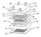
- FIG. 1Ais an exploded assembly view of apparatus 10 for cooling microelectronic devices such as semiconductor integrated circuits (also referred to herein as chips or semiconductor chips) that is fabricated in accordance with one or more embodiments of the present invention.
- support ring 19is a rigid retaining ring that supports top membrane 24 and bottom membrane 14 .
- the term support ringis not meant to limit embodiments of the present invention to configurations where a support ring refers to a structure having a generally circular shape.
- support ring 19refers to any support structure having a peripheral support portion with an empty area within the peripheral portion where the peripheral support structure may, for example and without limitation, be rectangular.
- support ring 19is made of a copper-tellurium alloy, and, in accordance with other embodiments, support ring 19 may be made of copper, brass, kovar, invar, aluminum nitride ceramic, glass ceramic, aluminum oxide or any rigid material.
- the material used to fabricate support ring 19i.e., the ring material
- the ring materialis selected, apart from its ability to provide rigid support, for its coefficient of thermal expansion (CTE).
- CTEcoefficient of thermal expansion
- the ring materialis preferably selected to have a low CTE.
- rigid support ring 19is preferably between 1.0 mm and 15.0 mm thick, for example and without limitation, rigid support ring 19 may be 5.0 mm thick.
- mechanically resilient membranes 14 and 24are attached to bottom and top surfaces of support ring 10 , respectively utilizing any one of a number of methods that are well known to those of ordinary skill in the art, for example and without limitation, by diffusion bonding.
- the material used to fabricate membranes 14 and 24i.e., the membrane material
- the membrane materialis selected for its thermal conductivity (a high thermal conductivity being preferred) and for its mechanical tensile strength and elongation.
- the membrane materialmay be a beryllium-copper spring alloy ASTM B534 or it may be selected from a group including sterling silver, coin silver, phosphor bronze, nitionol, Ni—Ti alloys, and various copper alloys such as alloy 186 (available from Olin Brass Company of Bridgeport, Conn.), and copper alloy ASTM B422.
- membrane 14comprises segments 11 of thermally conductive material separated by matrix 15 made of a mechanically resilient material.
- the mechanically resilient material of matrix 15is preferably thin, for example and without limitation, having a thickness between 25 and 100 micrometers. Segments 11 may be thicker than the mechanically resilient material of matrix 15 .
- segments 11may be formed from several layers of material. For example, in accordance with one embodiment, segments 11 include 50 micrometers of silver, 50 micrometers of a beryllium-copper alloy ASTM B534, and 50 micrometers of silver.
- membrane 24is fabricated like membrane 14 , and as such, is comprised of segments of material separated by a matrix made of mechanically resilient material.
- the mechanically resilient material of the matrix of membrane 24may be the same as the mechanically resilient material of matrix 15 .
- the material of segments of membrane 24may be the same as the material of segments 11 of membrane 14 .
- an array of thermally conductive posts 26are positioned between membranes 14 and 24 .
- posts 26are round or square in cross section.
- posts 26may have other shapes, for example and without limitation, more complex shapes, that also provide, or even improve, thermal contact with a cooling fluid.
- posts 26are in thermal contact with membranes 14 and 24 .
- each of posts 26is in thermal contact with (for example and without limitation by being attached to) one of thermally conductive segments 11 of membrane 14 to conduct heat from the segment through the post to cooling fluid circulating around the post.
- posts 26are disposed with spaces therebetween to enable passage of a cooling fluid.
- posts 26are copper alloy ASTM B152 cylinders that are area diffusion bonded directly to top membrane 24 and to bottom membrane 14 to form a thermal contact therebetween.
- posts 26are slideably attached to membrane 14 to form a thermal contact therebetween.
- apparatus 10includes resilient pad 22 that is positioned between manifold 18 and top membrane 24 .
- resilient pad 22is an elastomeric pad. Any one of a number of elastomers suitable for use in fabricating embodiments of the present invention are well known to those of ordinary skill in the art.
- manifold 30is made of plastic, but as one of ordinary skill in the art will readily appreciate, it may be made of any one of a number of suitable materials that are well known to those of ordinary skill in the art.
- resilient pad 22transmits force downward from manifold 18 onto membrane 24 .
- membrane 24transmits the force applied thereto, through the array of posts 26 , to individual ones of thermally conductive segments 11 of bottom membrane 14 .
- thermally conductive segments 11are held by mechanically resilient matrix 15 , they can move vertically to transmit force upwardly through posts thermally contacted (for example, by being attached) thereto and onto top membrane 24 .
- the mechanically resilient matrix of membrane 24enables upward flexure of top member 24 , which upward flexure is accommodated by resilient pad 22 .
- This capability of segments 11 to moveprovides bottom membrane 14 with compliance to enable it to conform to any device to which it is urged into contact.
- FIG. 1Bis a partial cross sectional view showing internal construction details of apparatus 10 .
- top membrane 24 and bottom membrane 14are joined to support ring 19 to form a cavity for cooling fluid that may be contained therebetween.
- each of thermally conductive posts 26such as post 28 shown in FIG. 1B , is thermally contacted at a top end to top membrane 24 and is thermally contacted at a bottom end to bottom membrane 14 .
- resilient pad 22 held between manifold 18 and top membrane 24accommodates upward flexure of top membrane 24 .
- cooling fluidis input, for example and without limitation, under pressure, into manifold 18 through inlet port 20 (one of ordinary skill in the art may determine an appropriate pressure routinely and without undue experimentation, for example and without limitation, in accordance with one or more embodiments a suitable pressure may be in a range from about 60 to about 80 psi).
- a suitable pressuremay be in a range from about 60 to about 80 psi.
- the cooling fluidis directed downward through aperture 13 in top membrane 24 , and then through aperture 12 into a passageway in support ring 19 .
- the cooling fluidthen flows through the array of posts 26 (i.e., past each of posts 26 ) to transfer heat by conduction from each post 26 to the cooling fluid.
- Cooling fluidsmay be gases or liquids.
- cooling fluids well known in the artinclude air, helium, water, water-glycol mixtures, Galden LS/155 (available from Solvay Solexis, Inc.), Fluorinert FC-77 (available from 3M Corporation), and others.
- one or more embodiments of the present inventionprovide method and apparatus for cooling microelectronic devices such as, for example and without limitation, a high power microelectronic device. More particularly, one or more embodiments of the present invention provide method and apparatus for cooling such a high power microelectronic device using a mechanically compliant heat sink that enables a rigid connection between a device and a heat sink attached thereto without generating thermally induced stresses in the connection.
- One or such embodiments of the present inventionare adapted for use in cooling a microelectronic device such as, for example and without limitation, a semiconductor chip, a packaged semiconductor chip, a multi-chip module, and a high power microelectronic device.
- the microelectronic devicemay be attached directly to membrane 14 on a side of membrane 14 (opposite the side on which the array of posts 26 are attached) using any one of a number of high conductivity die attach materials well known to those of ordinary skill in the art.
- the array of posts 26forms a heat sink for absorption of heat from the microelectronic device and transmits the heat to the cooling fluid.
- each of segments 11 of membrane 14may be rigidly attached to the microelectronic device by the die attach material.
- each of segments 11 of membrane 14substantially follows thermal expansion of the microelectronic device rather than expansion of membrane 14 so that differential expansion of the microelectronic device relative to that of membrane 14 is taken up by flexure of mechanically resilient regions 15 between each segment 11 .
- each of segments 11is made sufficiently small such that thermally induced stresses under such segment does not cause mechanical failure.
- the size of each of segments 11is small in comparison to the size of the microelectronic device to be cooled, so that a multitude of segments are needed to contact the microelectronic device.
- An appropriate size for segments 11 and an appropriate amount of resiliency for matrix 15can be determined by one of ordinary skill in the art routinely and without undue experimentation.
- a heat sinki.e., apparatus 10
- a microelectronic devicesuch as a semiconductor chip without inducing damaging thermal stresses between the heat sink and the chip.
- Membrane 14comprising an array of thermally conductive segments 11 is held in tension by attachment to rigid support ring 19 which, in a preferred embodiment, may be made of low CTE material.
- each of thermally conductive segments 11 in an array of thermally conductive segmentsis connected to segments directly adjacent to it by means of mechanically resilient connection or coupling elements that enable expansion of spacing between a segment and its adjacent segments.
- one such matrix of mechanically resilient connection or coupling elementsis provided by etching parallel grooves in top and bottom surfaces of membrane 14 , wherein grooves in the top surface are offset with respect to grooves in the bottom surface to form an undulating pattern in a cross section of membrane 14 .
- thermally conductive posts 16may be attached to a top side of membrane 14 so that one or more of posts 26 is attached to each of segments of membrane 14 .
- Posts 26provide a thermal path from membrane 14 , through posts 26 and into a cooling fluid that flows around posts 26 .
- membrane 14(comprising an array of thermally conductive segments 11 with a matrix 15 of mechanically resilient connection or coupling elements disposed therebetween) is held under tension by support ring 19 .
- membranes 14 and 24may be attached to support ring 19 under tension by heating these components, and by diffusion bonding the membranes to the support ring. Then, as the assembly cools, a desired tension is provided (a desired tension can be determined by one of ordinary skill in the art for any particular embodiment routinely and without undue experimentation). In operation, each of thermally conductive segments 11 expands laterally as the temperature of membrane 14 increases.
- the CTE of each of thermally conductive segments 11is greater than the CTE of support ring 19 .
- expansion of segments 11compresses the mechanically resilient connections between segments 11 to render the overall expansion of membrane 14 substantially equal to the expansion of support ring 19 to which it is attached.
- a rate of expansion of the array of thermally conductive segments 11is nearly matched to a low rate of expansion of support ring 19 .
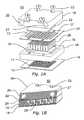
- FIG. 2Ais a cutaway view of a top of apparatus 30 adapted for testing microelectronic devices in accordance with one or more embodiments of the present invention.
- FIG. 2Bis a partial cross sectional view of apparatus 30 as cut along plane A-A′ of FIG. 2A .
- rigid support ring 32holds top membrane 42 in tension and bottom membrane 48 in tension.
- rigid support ring 32is made of invar, a low thermal expansion alloy of nickel-iron having a CTE of approximately 1.7 ⁇ 10 ⁇ 6 /° C.
- Top membrane 42 and bottom membrane 48are made of beryllium-copper alloy ASTM B534 having a relatively high CTE of approximately 17.7 ⁇ 10 ⁇ 6 /° C. Top membrane 42 and bottom membrane 48 are held in tension by rigid support ring 32 , which tension constrains thermal expansion of each membrane to follow the lower expansion rate of low CTE rigid support ring 32 .
- each of thermally conductive posts (also referred to herein as columns) 36is joined on its top surface to one of thermally conductive area segments 41 of top membrane 42 .
- each of thermally conductive area segments 41 of top membrane 42is surrounded by mechanically resilient matrix 43 formed in top membrane 42 .
- each of thermally conductive posts 36is joined on its bottom surface to one of thermally conductive area segments 49 of bottom membrane 48 .
- each of thermally conductive area segments 49 of bottom membrane 48is surrounded by mechanically resilient matrix 47 formed in bottom membrane 48 .
- posts 36are cylinders made of coin silver having a circular cross section and a length of 5.0 mm.
- apparatus 30includes resilient pad 40 which is disposed on a top surface of top membrane 42 and is held under a cavity in manifold 38 .
- resilient pad 40allows segments 41 of top membrane 42 to move compliantly in response to movement of posts 36 .
- resilient pad 40is an elastomeric pad made of silicone DC 577 (available from Dow Corning Corporation). Any one of a number of elastomers suitable for use in fabricating embodiments of the present invention are well known to those of ordinary skill in the art.
- resilient matrices 43 and 47 of top and bottom membranes 42 and 48respectively, in combination with resilient pad 40 disposed against top membrane 42 , provide a mechanically compliant surface at membrane 48 that facilitates testing of microelectronic devices with imperfect or warped surfaces.
- apparatus 30is cooled by circulating a cooling fluid therethrough.
- the cooling fluidis input, for example and without limitation, under pressure, to intake port 33 in manifold 38 which is sealed to top membrane 42 by “O” ring seal 35 .
- manifold 30is made of plastic, but as one of ordinary skill in the art will readily appreciate, it may be made of any one of a number of suitable materials that are well known to those of ordinary skill in the art.
- the cooling fluidis directed downward through an aperture (not shown) in top membrane 42 , and then through aperture 37 in support ring 32 to a passageway therein.
- the cooling fluidthen flows through the array of posts 36 (i.e., past each of posts 36 ) disposed in a cavity of support ring 32 , to transfer heat by conduction from each post 36 to the cool fluid. Then, the cooling fluid exits the cavity by passing out through another passageway to aperture 34 in support ring 32 , through aperture 34 in top membrane 42 , and into manifold 30 . Next, the cooling fluid exits from an outlet port (not shown) in manifold 30 . Although the cutaway view does not show all of top membrane 42 , top membrane 42 seals apparatus 30 to prevent leakage of cooling fluid.
- one or more embodiments of the present inventionprovide method and apparatus for testing microelectronic devices such as, for example and without limitation, a high power microelectronic device. More particularly, one or more such embodiments of the present invention provide method and apparatus for testing such a high power microelectronic device using a mechanically compliant heat sink. In accordance with one or more such embodiments, during testing, the mechanically compliant heat sink is detachably mounted to the microelectronic device by applying pressure to urge the heat sink, for example, downward, onto a top surface of the microelectronic device.
- a mechanically compliant membrane(forming a bottom surface of the heat sink) makes contact with the top surface of the microelectronic device.
- the membrane and associated cooling elements of the heat sinkare mechanically compliant and enable the bottom surface of the heat sink to deform in response to imperfections (such as particles, warping, bowing and surface contours) on the microelectronic device.
- imperfectionssuch as particles, warping, bowing and surface contours
- thermal conduction between the heat sink and the microelectronic deviceis increased by compliant deformation of the bottom surface of the heat sink, which compliant deformation minimizes spacing between each element of the surface of the microelectronic device and juxtaposed area elements of the bottom surface of the heat sink.
- the heat sinkis detached from the device, and it may then be urged into contact with another device to be tested.
- the mechanically resilient membrane on the bottom of the heat sinkcompliantly deforms to accommodate imperfections on the next device to be tested. As one or ordinary skill in the art can readily appreciate, because the membrane is mechanically resilient, it can compliantly deform repeatedly for each device being tested without damage to the membrane or the head sink.
- the bottom surface of the heat sinkdeforms to fill the spaces between the heat sink and an imperfect surface of the device, it eliminates a need for an additional compliant gap filler material used in the prior art. As a result, one or more such embodiments provide high thermal conductivity connections to the device.
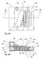
- FIG. 3Ais a cross sectional view of apparatus 60 that is fabricated in accordance with one or more embodiments of the present invention and that may be used to cool a microelectronic device such as, for example and without limitation, a semiconductor device. As shown in FIG. 3A , apparatus 60 is rigidly attached to semiconductor device 70 . Apparatus 60 may be attached to apparatus 60 using any one of a number of methods that are well known to those of ordinary skill in the art and which provide a predetermined thermal conductivity between semiconductor device 70 and apparatus 60 .
- cooling fluidfor example and without limitation, pressurized cooling fluid
- cooling fluidflows around each one of posts 51 .
- top membrane 58 and bottom membrane 52are held in tension by support ring 50 which is made of a rigid, low expansion material.
- each element of the arrayis able to move resiliently and, as such, provides a measure of mechanical compliance to a segment, for example, segment 53 , that thermally contacts semiconductor device 70 under test.
- each element of the arrayfunctions to help prevent bottom membrane 52 from bowing downward under pressure from the cooling fluid.
- posts in the arrayfor example, post 51
- posts in the arrayare tied to both top membrane 58 and bottom membrane 52 , and because of this, the membranes are inhibited from being distorted by pressure in the cooling fluid while allowing compliant movement of segments, for example, segment 53 , to which they are attached.
- FIG. 3Bis a cross sectional view of a portion of apparatus 60 , including membrane 52 , which shows mechanically resilient connections between thermally conductive segments 72 of membrane 52 at room temperature.
- the mechanically resilient connectionsare embodied as an undulating link between segment 72 and its adjacent segments.
- the undulating linkcomprises in sequence from right to left: thin lateral section 74 , vertical section 75 , lateral section 76 , vertical section 71 , and lateral section 73 .
- each thermally conductive segment 72 of bottom membrane 52is attached to a top surface of semiconductor device 70 by means of layer 78 of die attach material. Because the lateral dimensions of segment 72 are relatively small compared to the area of the top surface of device 70 , layer 78 of die attach material may be thin and relatively rigid without inducing a damaging level of thermal stress in device 70 .
- each thermally conductive segment 72is a square wherein a length of a side is in a range between about 0.3 mm and about 5.0 mm, for example and without limitation, in a range between about 1.0 and about 2.5 mm.
- the die attach materialmay be selected from any one of a number of materials that are well known to those of ordinary skill in the art such as, for example, a group of materials including gold-tin alloy, gold-germanium alloy, gold-silicon alloy, lead-tin solder, indium alloys, silver filled epoxy, and particle filled adhesive polymers.
- FIG. 3Cis a cross sectional view of a portion of apparatus 60 , including membrane 52 , which shows mechanically resilient connections between thermally conductive segments 82 of membrane 52 at an elevated temperature above room temperature.
- the mechanically resilient connectionsare embodied as an undulating link between segment 82 and its adjacent segments.
- the undulating linkcomprises in sequence from right to left: thin lateral section 84 , vertical section 85 , lateral section 86 , vertical section 81 , and lateral section 83 .
- each thermally conductive segment 82 of bottom membrane 52is attached to a top surface of semiconductor device 70 by means of a thin layer 88 of die attach material.
- the elevated operating temperaturecauses thermally conductive segment 82 to expand more than its juxtaposed portion of the top surface of semiconductor device 70 .
- This differential expansiondistorts a region around die attach material 88 and also distorts elements 81 and 85 of the mechanically resilient connection, i.e., the undulating link.
- a center point of each of the thermally conductive segmentsremains unmoved with respect to juxtaposed portions of the top surface of semiconductor device 70 .
- the CTE of membrane 52as measured at center points of its thermally conductive segments, is substantially the same as that of semiconductor device 70 to which it is attached. That is, firstly, each of segments 82 is able to move in response to thermal expansion of semiconductor device 70 without causing a damaging amount of stress in die attach material 88 .
- each of segments 82is also able to undergo thermal expansion 89 without significantly moving the center of segment 82 with respect to device 70 .
- the center of each of segments 82remains substantially fixed with respect to the adjacent portion of juxtaposed device 70 .
- FIG. 4Ais top view of a portion of membrane 90 used to fabricate one or more embodiments of the present invention in which membrane 90 is divided into thermally conductive segments, for example, like thermally conductive segment 94 that has a hexagonal shape, which segments are arranged in a hexagonal pattern. Further, as shown in FIG. 4A , each segment is connected to adjacent segments by mechanically resilient connection elements, for example, like resilient connection element 98 . In addition, as will be described in more detail below, a cylindrical post, for example, like cylindrical post 100 shown in FIGS. 4B and 4D , is attached to each thermally conductive segment, for example, like thermally conductive segment 94 .
- FIG. 4Bis a cross sectional view of a portion of an apparatus that is fabricated in accordance with one or more embodiments of the present invention and that uses membrane 90 , the cross sectional view being along the cut plane B-B′ of FIG. 4A .
- conductive postsfor example, conductive post 100
- thermally conductive segmentsfor example, thermally conductive segment 104
- thermally conductive segment 112for example, thermally conductive segment 112
- conductive segment 104is connected to adjacent segments in top membrane 101 by an undulating link formed by channel 106 in a top surface of top membrane 101 and two channels 102 in a bottom surface of top membrane 101 , which two channels 102 are offset laterally from channel 106 .
- thermally conductive segment 112is connected to adjacent segments in bottom membrane 103 by an undulating link formed by channel 110 in a bottom surface of membrane 103 and two channels 108 in a top surface of bottom membrane 103 , which two channels 108 are offset laterally from channel 110 .
- FIG. 4Cshows details of a resilient connection element which is disposed in bottom membrane 103 and shown in FIG. 4B .
- an undulating link which connects thermally conductive segment 112 to adjacent segmentsincludes: (a) channel 110 in the bottom surface of bottom membrane 103 ; (b) laterally offset, relatively parallel channels 108 in the top surface of bottom membrane 103 ; and (c) relatively vertical elements 114 and 116 .
- the degree of resilience of the undulating linkmay be increased by increasing the number of parallel channels in membrane 103 , and may be decreased by reducing the number of parallel channels in membrane 103 .
- thermally conductive segmentsfor example, thermally conductive segment 112 may include a layer of silver on top and/or bottom surfaces, which layers may be applied by plating in accordance with any one of a number of methods well known to those of ordinary skill in the art.
- a layerfor example, a plated layer, may overlay in part channels 110 and 108 in membrane 103 .
- FIG. 4Dis a cross sectional view showing the portion shown in FIG. 4B where top membrane 131 and bottom membrane 133 are held in tension.
- thermally conductive segmentsare connected to adjacent segments in top membrane 131 and in bottom membrane 133 by undulating links. For example, as shown in FIG.
- an undulating link in top membrane 131is formed by channel 122 in a top surface of top membrane 131 and two channels 126 in a bottom surface of top membrane 131 , which two channels 126 are offset laterally from channel 122 ; and (b) an undulating link in bottom membrane 133 is formed by channel 112 in bottom surface of bottom membrane 133 and two channels 108 in a top surface of bottom membrane 133 , which two channels 128 are offset laterally from channel 112 .
- Each of the undulating links between each of segments 112is stretched so as to hold membrane 133 in tension laterally.
- FIG. 4Eis a cross sectional view showing the portion shown in FIG. 4C where top membrane 131 and bottom membrane 133 are held in tension.
- an undulating link which connects thermally conductive segment 112 to adjacent segmentsincludes: (a) channel 130 in the bottom surface of bottom membrane 133 ; (b) laterally offset, relatively parallel channels 128 on the top surface of bottom membrane 133 ; and (c) relatively vertical elements 134 and 136 .
- elements 134 and 136are distorted by tension in membrane 133 .
- resilience of the undulating linkis due, at least in part, by the resilience to distortion of portions such as elements 134 and 136 .
- FIGS. 5A , 5 B and 5 Cshow thermally conductive posts that are fabricated in accordance with one or more embodiments of the present invention that enhance thermal transfer to a cooling fluid.
- thermally conductive post 140comprises tube 142 having a hollow core and slots 144 disposed in a side wall of the tube.
- slots 144allow cooling fluid to circulate into the tube, increasing surface area in contact with the cooling fluid and thereby increasing transfer of heat from post 140 to the cooling fluid.
- An appropriate number, size, and positioning of slotsmay be determined by one of ordinary skill in the art routinely and without undue experimentation.
- thermally conductive post 146comprises post 148 having grooves 150 disposed in a side wall of the post wherein slots 150 are spiral grooves.
- the grooves 150increase heat transfer from post 146 to a surrounding cooling fluid by increasing surface area of the post that is in contact with the fluid and by acting to mix the fluid flowing past the post.
- Post 146 of FIG. 5Bmay have an interior hole 148 to form a hollow tube.
- the spiral grooves 150may be cut through tube 146 to form helical springs in the wall of the tube.
- the helical springs of thermally conductive post 146provide spring action so that post 146 provides a vertical resilience that enhances the resilience of any membrane attached thereto.
- the hollow tubeallows electrical leads from a temperature sensor to be routed through a portion of the tube length, to allow positioning a thermal sensor such as a thermocouple directly on the membrane in order to obtain accurate temperature measurements.
- thermally conductive post 152comprises multiple legs 158 that are attached to flat portion 154 .
- flat portion 154increases heat flow from legs 158 to any membrane attached to flat portion 154 .
- slots 156 disposed between legs 158allow cooling fluid to contact a larger surface area of post 152 , and thereby enable increased heat flow from post 152 to the cooling fluid.
- FIGS. 5A , 5 B and 5 Cmay be fabricated of any one of a number of thermally conductive materials that are well known to those of ordinary skill in the art using any one of a number of fabrication methods that are well known in the art.
- postsmay be coated with a high thermal conductivity material such as, for example and without limitation, diamond, which may be deposited by any one of a number of methods that are well known to those of ordinary skill in the art such as, for example and without limitation, chemical vapor deposition.
- FIGS. 6A and 6Bare cross sectional views of portions of apparatus that are fabricated in accordance with one or more embodiments of the present invention showing mechanically resilient sections around thermally conductive segments affixed to thermally conductive posts.
- thermally conductive segment 164 of membrane 162is permanently attached to thermally conductive post 160 , such attachment may be provided using any one of a number of methods that are well known to those of ordinary skill in the art.
- resilient connection 168is an undulation of membrane 162 , wherein membrane 162 may be formed using any one of a number of methods that are well known to those of ordinary skill in the art such as, for example and without limitation, by plating nickel onto a temporary mandrel. In accordance with one or more such embodiments, slots in the mandrel may be used to form undulations in the plated membrane that provide resilient connections like resilient connection 168 .
- Dashed line 166 in FIG. 6Ashows the undulation in membrane 162 as initially formed, i.e., without membrane 162 being under tension, and the undulation identified as resilient connection 168 represents the undulation after membrane 162 is placed under tension. In accordance with one or more embodiments of the present invention, under tension, the undulation stretches to provide resilience in its connection between thermally conductive segment 164 and adjacent thermally conductive segments.
- thermally conductive segment 174 of membrane 172is permanently attached to thermally conductive post 170 , such attachment may be provided using diffusion bonding or by using any one of a number of methods that are well known to those of ordinary skill in the art.
- resilient connection 184is an undulation of membrane 172 , wherein the undulations may be formed using any one of a number of methods that are well known to those of ordinary skill in the art such as, for example and without limitation, by cutting grooves in the surface of the membrane by embossing, by micro-machining, by laser machining, or by reactive ion etching.
- undulationsfor example the undulations in resilient connection 184 , may be formed by electrochemically etching grooves 176 and 178 into a top surface of membrane 172 and groove 180 into a bottom surface of membrane 172 in accordance with any one of a number of methods that are well known to those of ordinary skill in the art.
- grooves 176 and 178are parallel to groove 180 , and are displaced laterally therefrom to form an undulation in a surface of membrane 172 .
- undulation 184stretches to provide resilience in its connection between thermally conductive segment 174 and adjacent thermally conductive segments.
- FIG. 7Ais a cross sectional view of an arrangement useful in testing high power microelectronic device 206 that includes mechanically compliant heat sink 200 that is fabricated in accordance with one or more embodiments of the present invention where microelectronic device 206 is flat. As such, FIG. 7A shows mechanically compliant heat sink 200 in contact with an ideal microelectronic device 206 .
- FIG. 7Bshows a cross sectional view of the arrangement where microelectronic device 236 is warped. As such, FIG. 7B shows mechanically compliant heat sink 230 in contact with a warped and distorted microelectronic device 236 .
- microelectronic device 206is attached to printed wiring substrate 200 by means of solder bumps 204 .
- printed wiring substrate 224has a ball grid array of contacts 202 on its bottom surface.
- a downward force applied to manifold 222 of mechanically compliant heat sink 200urges membrane 210 into contact with a top surface of device 206 by transmitting the force through resilient pad 220 , membrane 214 , posts 216 , and membrane 210 .
- support ring 212holds membranes 210 and 214 under tension while allowing them to move.
- Heat from device 206is conducted through gap 208 between the top surface of device 206 and membrane 210 , and into thermally conductive posts 216 where it is carried away by a cooling fluid flowing around and between the posts. Because gap 208 is very thin, its thermal resistance is small. In accordance with one or more embodiments of the present invention, the thermal resistance of gap 208 may be further reduced by filling gap 208 with helium, water, isopropyl alcohol, glycol, glycerin or other relatively conductive fluid materials in accordance with any one of a number of methods that are well known to those of ordinary skill in the art.
- microelectronic device 236is warped and is attached to printed wiring substrate 254 by means of solder balls 234 .
- device 236 and printed wiring substrate 254are warped. This is often caused by thermal stresses in printed wiring substrate 254 or by thermally induced stresses between device 236 and printed wiring substrate 254 .
- membrane 240compliantly bends to conform to the warped surface of device 236 , thereby reducing gap 238 therebetween. As a result, good thermal contact is maintained between device 236 and mechanically compliant heat sink 230 .
- the upwardly warped surface of device 236causes compliant membrane 240 to distort upwardly, thereby increasing pressure on posts 246 in a center portion of mechanically compliant heat sink 230 .
- posts 246push upwardly on membrane 244 , compressing resilient pad 250 against manifold 252 .
- compression of resilient pad 250allows membranes 240 and 244 and the array of posts 246 attached thereto to conform compliantly to fit the warped surface of device 236 .
- support ring 242holds membranes 244 and 240 in tension while allowing them to move to conform compliantly to the warped surface of device 236 .
- gap 238 between warped device 236 and compliant membrane 240is reduced, and thermal conduction therebetween is increased.
- thermal resistance of gap 238may be reduced by filling gap 238 with helium, water, isopropyl alcohol, glycol, glycerin or other relatively conductive fluid materials in accordance with any one of a number of methods that are well known to those of ordinary skill in the art.
- FIG. 8shows system 280 that is fabricated in accordance with one or more embodiments of the present invention for cooling high power microelectronic device 250 .
- device 250is attached directly to mechanically compliant thermal heat sink 256 that is fabricated in accordance with one or more embodiments of the present invention.
- device 250is mounted on daughter card 252 which is, in turn, attached to system board 254 .
- heat generated in device 250is conducted through mechanically compliant thermal heat sink 256 to a cooling fluid flowing therethrough.
- the cooling fluidenters manifold 258 from a circulating system.
- Manifold 258directs the cooling fluid to flow through mechanically compliant thermal heat sink 256 .
- the cooling fluidflows through tubing 268 back to pump 250 where it is pressurized and fed through tubing 262 into heat sink 264 where heat is extracted therefrom.
- the cooling fluidis then fed through tubing 266 back to manifold 258 .
- reservoir 278holds excess cooling fluid, and tubing 272 and 276 connect reservoir 278 to circulating fluid flow 270 .
- valve 274is activated to allow cooling fluid to flow into and out of reservoir 278 .
- Operation of circulating cooling fluid systemsis well known in the art, and such systems may be fabricated in accordance with any one of a number of methods that are well known to those of ordinary skill in the art. Further, in light of the detailed described provided herein, one of ordinary skill in the art can readily determine how such systems may be used in conjunction with mechanically compliant thermal heat sinks that are fabricated in accordance with one or more embodiments of the present invention.
- microelectronic device 250will undergo cycles of heating and cooling that induce mechanical expansion, warpage and movement of device 250 .
- compliance of mechanically compliant thermal heat sink 256accommodates these mechanical distortions without impairing thermal contact between heat sink 256 and device 250 .
- the top membranemay not comprise thermally conductive segments and mechanically resilient connections disposed between the thermally conductive segments.
- one or more such embodimentsinclude the top membrane being replaced by a solid block.
- the ring structuremay have one side being solid so that that side would serve as the solid block.
Landscapes
- Physics & Mathematics (AREA)
- Condensed Matter Physics & Semiconductors (AREA)
- General Physics & Mathematics (AREA)
- Engineering & Computer Science (AREA)
- Computer Hardware Design (AREA)
- Microelectronics & Electronic Packaging (AREA)
- Power Engineering (AREA)
- Cooling Or The Like Of Semiconductors Or Solid State Devices (AREA)
Abstract
Description
Claims (23)
Priority Applications (1)
| Application Number | Priority Date | Filing Date | Title |
|---|---|---|---|
| US11/415,901US7849914B2 (en) | 2006-05-02 | 2006-05-02 | Cooling apparatus for microelectronic devices |
Applications Claiming Priority (1)
| Application Number | Priority Date | Filing Date | Title |
|---|---|---|---|
| US11/415,901US7849914B2 (en) | 2006-05-02 | 2006-05-02 | Cooling apparatus for microelectronic devices |
Publications (2)
| Publication Number | Publication Date |
|---|---|
| US20070256810A1 US20070256810A1 (en) | 2007-11-08 |
| US7849914B2true US7849914B2 (en) | 2010-12-14 |
Family
ID=38660177
Family Applications (1)
| Application Number | Title | Priority Date | Filing Date |
|---|---|---|---|
| US11/415,901Active2029-09-13US7849914B2 (en) | 2006-05-02 | 2006-05-02 | Cooling apparatus for microelectronic devices |
Country Status (1)
| Country | Link |
|---|---|
| US (1) | US7849914B2 (en) |
Cited By (24)
| Publication number | Priority date | Publication date | Assignee | Title |
|---|---|---|---|---|
| US20090301692A1 (en)* | 2008-06-06 | 2009-12-10 | Hironori Oikawa | Electronic Apparatus Cooling Device |
| US20100254140A1 (en)* | 2009-04-07 | 2010-10-07 | Fong-Yuan Wen | Lamp holder of led streetlamp with heat-conducting and heat-dissipating capability |
| US20100307730A1 (en)* | 2009-06-03 | 2010-12-09 | High Conduction Scientific Co., Ltd. | Liquid-cooled heat dissipating device and method of making the same |
| US20120061059A1 (en)* | 2010-09-09 | 2012-03-15 | Taiwan Semiconductor Manufacturing Company, Ltd. | Cooling mechanism for stacked die package and method of manufacturing the same |
| US20120120599A1 (en)* | 2010-11-12 | 2012-05-17 | Semicaps Pte Ltd | Apparatus and method for cooling a semiconductor device |
| WO2012121696A1 (en)* | 2011-03-07 | 2012-09-13 | Aavid Thermalloy, Llc | Thermal transfer device with spiral fluid pathways |
| US8987891B2 (en) | 2012-03-05 | 2015-03-24 | Centipede Systems, Inc. | Heat sink apparatus for microelectronic devices |
| CN105190874A (en)* | 2013-05-09 | 2015-12-23 | 三菱电机株式会社 | Semiconductor module and semiconductor device |
| US9265177B2 (en) | 2013-03-08 | 2016-02-16 | International Business Machines Corporation | Fabricating multi-component electronic module with integral coolant-cooling |
| US20160093788A1 (en)* | 2014-09-29 | 2016-03-31 | Hitachi, Ltd. | Cooling Structure of Heating Element and Power Conversion Device |
| US9343436B2 (en) | 2010-09-09 | 2016-05-17 | Taiwan Semiconductor Manufacturing Company, Ltd. | Stacked package and method of manufacturing the same |
| US9917034B2 (en) | 2014-09-26 | 2018-03-13 | Semicaps Pte Ltd | Method and apparatus for cooling a semiconductor device |
| US10157814B1 (en) | 2017-06-27 | 2018-12-18 | International Business Machines Corporation | Compliant heat sink |
| US10168108B2 (en)* | 2014-09-29 | 2019-01-01 | International Business Machines Corporation | Pin fin compliant heat sink with enhanced flexibility |
| US20190004573A1 (en)* | 2017-06-29 | 2019-01-03 | Intel Corporation | Methods of direct cooling of packaged devices and structures formed thereby |
| US20190285362A1 (en)* | 2018-03-13 | 2019-09-19 | Nec Corporation | Cooling structure and mounting structure |
| US10978313B2 (en) | 2018-02-20 | 2021-04-13 | International Business Machines Corporation | Fixture facilitating heat sink fabrication |
| US10991639B2 (en) | 2016-04-01 | 2021-04-27 | International Business Machines Corporation | Compliant Pin Fin heat sink with base integral pins |
| US20210315130A1 (en)* | 2020-04-07 | 2021-10-07 | Abb Schweiz Ag | Cooling Element And Method Of Manufacturing A Cooling Element |
| US20220011836A1 (en)* | 2021-09-24 | 2022-01-13 | Intel Corporation | Flow enhancement structure to increase bandwidth of a memory module |
| US11355418B2 (en)* | 2019-09-29 | 2022-06-07 | Taiwan Semiconductor Manufacturing Company, Ltd. | Package structure and manufacturing method thereof |
| US11355420B2 (en)* | 2018-06-27 | 2022-06-07 | Fuji Electric Co., Ltd. | Cooling apparatus, semiconductor module, and vehicle |
| US11516949B2 (en)* | 2018-03-13 | 2022-11-29 | Nissan Motor Co., Ltd. | Power convertor |
| US20230200009A1 (en)* | 2021-12-22 | 2023-06-22 | Baidu Usa Llc | Two phase immersion system with local fluid accelerations |
Families Citing this family (46)
| Publication number | Priority date | Publication date | Assignee | Title |
|---|---|---|---|---|
| US7492595B2 (en)* | 2005-03-31 | 2009-02-17 | Tecnisco Limited | Semiconductor cooling device and stack of semiconductor cooling devices |
| US20080230208A1 (en)* | 2007-03-22 | 2008-09-25 | Claus Nygaard Rasmussen | Liquid Cooling System Cold Plate Assembly |
| JP4953206B2 (en)* | 2007-06-08 | 2012-06-13 | 株式会社デンソー | Heat exchange member and heat exchange device |
| EP2166569A1 (en)* | 2008-09-22 | 2010-03-24 | ABB Schweiz AG | Cooling device for a power component |
| US20100200197A1 (en)* | 2009-02-09 | 2010-08-12 | International Business Machines Corporation | Liquid cooled compliant heat sink and related method |
| US7782616B1 (en)* | 2009-04-23 | 2010-08-24 | Delphi Technologies, Inc. | Heat-dissipating component having stair-stepped coolant channels |
| US20100296249A1 (en)* | 2009-05-19 | 2010-11-25 | Beijing AVC Technology Research Center Co., Ltd. | Micro passage cold plate device for a liquid cooling radiator |
| FI122415B (en)* | 2009-09-17 | 2012-01-13 | Abb Oy | Cooled base for electrical components |
| US20110079376A1 (en)* | 2009-10-03 | 2011-04-07 | Wolverine Tube, Inc. | Cold plate with pins |
| FR2955971B1 (en)* | 2010-02-01 | 2012-03-09 | Areva T & D Sas | HEAT EXCHANGER, IN PARTICULAR FOR A POWER SEMICONDUCTOR |
| JP4951094B2 (en)* | 2010-02-16 | 2012-06-13 | 株式会社東芝 | Electronic equipment cooling structure |
| US20120068571A1 (en)* | 2010-09-20 | 2012-03-22 | Industrial Technology Research Institute | Capacitive micromachined ultrasonic transducer |
| TW201217737A (en)* | 2010-10-26 | 2012-05-01 | Inventec Corp | A heat exchange chamber for liquid state cooling fluid |
| WO2012131519A1 (en)* | 2011-03-25 | 2012-10-04 | Koninklijke Philips Electronics N.V. | Thermal interface pad material with perforated liner |
| WO2012157247A1 (en)* | 2011-05-16 | 2012-11-22 | 富士電機株式会社 | Cooler for use in semiconductor module |
| US9901013B2 (en) | 2011-06-27 | 2018-02-20 | Ebullient, Inc. | Method of cooling series-connected heat sink modules |
| US9832913B2 (en) | 2011-06-27 | 2017-11-28 | Ebullient, Inc. | Method of operating a cooling apparatus to provide stable two-phase flow |
| US9901008B2 (en) | 2014-10-27 | 2018-02-20 | Ebullient, Inc. | Redundant heat sink module |
| US9854714B2 (en) | 2011-06-27 | 2017-12-26 | Ebullient, Inc. | Method of absorbing sensible and latent heat with series-connected heat sinks |
| US9854715B2 (en) | 2011-06-27 | 2017-12-26 | Ebullient, Inc. | Flexible two-phase cooling system |
| US9848509B2 (en) | 2011-06-27 | 2017-12-19 | Ebullient, Inc. | Heat sink module |
| US20130056176A1 (en)* | 2011-08-26 | 2013-03-07 | Mikros Manufacturing, Inc. | Heat Exchanger with Controlled Coefficient of Thermal Expansion |
| GB2503494A (en)* | 2012-06-29 | 2014-01-01 | Bae Systems Plc | Heat exchanger comprising a fibre reinforced polymer composite |
| US9035452B2 (en)* | 2012-08-07 | 2015-05-19 | General Electric Company | Electronic device cooling with autonomous fluid routing and method of assembly |
| JP5880519B2 (en)* | 2013-10-21 | 2016-03-09 | トヨタ自動車株式会社 | In-vehicle electronic device |
| JP6191660B2 (en)* | 2014-08-05 | 2017-09-06 | 株式会社豊田中央研究所 | Thermal conductor, semiconductor device provided with thermal conductor |
| KR20160043512A (en)* | 2014-10-13 | 2016-04-21 | 조한용 | Fin tube heat sink and method for manufacturing the same |
| US9852963B2 (en) | 2014-10-27 | 2017-12-26 | Ebullient, Inc. | Microprocessor assembly adapted for fluid cooling |
| US20160116218A1 (en) | 2014-10-27 | 2016-04-28 | Ebullient, Llc | Heat exchanger with helical passageways |
| US20160120059A1 (en) | 2014-10-27 | 2016-04-28 | Ebullient, Llc | Two-phase cooling system |
| WO2016069414A1 (en)* | 2014-10-27 | 2016-05-06 | Ebullient, Llc | Flexible cooling line assembly |
| US10184699B2 (en) | 2014-10-27 | 2019-01-22 | Ebullient, Inc. | Fluid distribution unit for two-phase cooling system |
| US20180139865A1 (en)* | 2016-11-17 | 2018-05-17 | Nathanael Draht | Microstructure water cooling unit for cooling of an electrical or electronic component that already includes a flow diverter and a flow distributor |
| US10615100B2 (en)* | 2016-12-08 | 2020-04-07 | Toyota Motor Engineering & Manufacturing North America, Inc. | Electronics assemblies and cooling structures having metalized exterior surface |
| JP6237942B1 (en)* | 2017-01-30 | 2017-11-29 | 富士通株式会社 | Immersion cooling device |
| US10159165B2 (en)* | 2017-02-02 | 2018-12-18 | Qualcomm Incorporated | Evaporative cooling solution for handheld electronic devices |
| US10881019B2 (en)* | 2018-03-09 | 2020-12-29 | Fujitsu Limited | Cooling apparatus |
| US11036030B2 (en)* | 2018-06-15 | 2021-06-15 | Silicon Light Machines Corporation | MEMS posting for increased thermal dissipation |
| US11817371B2 (en)* | 2018-09-26 | 2023-11-14 | Intel Corporation | Non-planar conforming heatsink |
| US10971427B2 (en)* | 2019-02-04 | 2021-04-06 | Dell Products L.P. | Heatsink for information handling system |
| US10905028B2 (en)* | 2019-05-07 | 2021-01-26 | International Business Machines Corporation | Structure for eliminating the impact of cold plate fouling |
| US11158566B2 (en)* | 2019-05-24 | 2021-10-26 | Google Llc | Integrated circuit with a ring-shaped hot spot area and multidirectional cooling |
| DE102019134565A1 (en)* | 2019-12-16 | 2021-06-17 | HELLA GmbH & Co. KGaA | Housing for a converter and converter, in particular a DC converter with such a housing |
| CN113758328B (en) | 2021-08-13 | 2022-06-17 | 中南大学 | Composite VC radiator containing copper/diamond composite-configuration liquid absorption cores and preparation method thereof |
| US11910578B2 (en)* | 2021-09-23 | 2024-02-20 | Contitech Techno-Chemie Gmbh | Vehicle electronics cooling systems and methods |
| CN114187838B (en)* | 2021-12-14 | 2022-07-15 | 深圳市瀚达美电子有限公司 | Direct type energy-saving vehicle-mounted backlight module with active driving device and driving method |
Citations (47)
| Publication number | Priority date | Publication date | Assignee | Title |
|---|---|---|---|---|
| US4193445A (en)* | 1978-06-29 | 1980-03-18 | International Business Machines Corporation | Conduction cooled module |
| US4226281A (en) | 1979-06-11 | 1980-10-07 | International Business Machines Corporation | Thermal conduction module |
| US4235283A (en) | 1979-12-17 | 1980-11-25 | International Business Machines Corporation | Multi-stud thermal conduction module |
| US4381032A (en)* | 1981-04-23 | 1983-04-26 | Cutchaw John M | Apparatus for cooling high-density integrated circuit packages |
| US4468717A (en) | 1982-06-09 | 1984-08-28 | Sperry Corporation | Apparatus for cooling integrated circuit chips |
| US4500945A (en) | 1982-07-23 | 1985-02-19 | International Business Machines Corporation | Directly sealed multi-chip module |
| US4639829A (en) | 1984-06-29 | 1987-01-27 | International Business Machines Corporation | Thermal conduction disc-chip cooling enhancement means |
| US4685211A (en) | 1984-08-17 | 1987-08-11 | Nec Corporation | Method of producing a cooled electronic assembly |
| US4693303A (en) | 1985-06-20 | 1987-09-15 | Nec Corporation | Liquid cooling module with springy contact elements and an aperture plate slidable thereover |
| US4721996A (en) | 1986-10-14 | 1988-01-26 | Unisys Corporation | Spring loaded module for cooling integrated circuit packages directly with a liquid |
| US4729060A (en) | 1984-01-26 | 1988-03-01 | Fujitsu Limited | Cooling system for electronic circuit device |
| US4730666A (en) | 1986-04-30 | 1988-03-15 | International Business Machines Corporation | Flexible finned heat exchanger |
| US4730665A (en)* | 1983-07-14 | 1988-03-15 | Technology Enterprises Company | Apparatus for cooling high-density integrated circuit packages |
| US4748495A (en) | 1985-08-08 | 1988-05-31 | Dypax Systems Corporation | High density multi-chip interconnection and cooling package |
| US4750086A (en) | 1985-12-11 | 1988-06-07 | Unisys Corporation | Apparatus for cooling integrated circuit chips with forced coolant jet |
| US4783721A (en) | 1985-10-04 | 1988-11-08 | Fujitsu Limited | Cooling system for an electronic circuit device |
| US4794981A (en) | 1986-04-09 | 1989-01-03 | Nec Corporation | Cooling system |
| US4800956A (en) | 1986-04-25 | 1989-01-31 | Digital Equipment Corporation | Apparatus and method for removal of heat from packaged element |
| US4847731A (en) | 1988-07-05 | 1989-07-11 | The United States Of America As Represented By The Secretary Of The Navy | Liquid cooled high density packaging for high speed circuits |
| US4854377A (en) | 1985-11-19 | 1989-08-08 | Nec Corporation | Liquid cooling system for integrated circuit chips |
| US4879629A (en) | 1988-10-31 | 1989-11-07 | Unisys Corporation | Liquid cooled multi-chip integrated circuit module incorporating a seamless compliant member for leakproof operation |
| US4884167A (en) | 1987-11-09 | 1989-11-28 | Nec Corporation | Cooling system for three-dimensional IC package |
| US4884169A (en) | 1989-01-23 | 1989-11-28 | Technology Enterprises Company | Bubble generation in condensation wells for cooling high density integrated circuit chips |
| US4933747A (en)* | 1989-03-27 | 1990-06-12 | Motorola Inc. | Interconnect and cooling system for a semiconductor device |
| US4938279A (en) | 1988-02-05 | 1990-07-03 | Hughes Aircraft Company | Flexible membrane heat sink |
| US4942497A (en) | 1987-07-24 | 1990-07-17 | Nec Corporation | Cooling structure for heat generating electronic components mounted on a substrate |
| US4964458A (en) | 1986-04-30 | 1990-10-23 | International Business Machines Corporation | Flexible finned heat exchanger |
| US5022462A (en)* | 1986-04-30 | 1991-06-11 | International Business Machines Corp. | Flexible finned heat exchanger |
| US5083373A (en) | 1986-04-25 | 1992-01-28 | Hamburgen William R | Method for providing a thermal transfer device for the removal of heat from packaged elements |
| US5168348A (en)* | 1991-07-15 | 1992-12-01 | International Business Machines Corporation | Impingment cooled compliant heat sink |
| US5228502A (en)* | 1991-09-04 | 1993-07-20 | International Business Machines Corporation | Cooling by use of multiple parallel convective surfaces |
| US5349823A (en) | 1992-02-14 | 1994-09-27 | Intel Corporation | Integrated refrigerated computer module |
| US5360993A (en) | 1991-10-21 | 1994-11-01 | Nec Corporation | Cooling unit capable of speedily cooling an integrated circuit chip |
| US5388635A (en) | 1990-04-27 | 1995-02-14 | International Business Machines Corporation | Compliant fluidic coolant hat |
| US5517753A (en) | 1995-04-06 | 1996-05-21 | International Business Machines Corporation | Adjustable spacer for flat plate cooling applications |
| US5586005A (en) | 1995-03-16 | 1996-12-17 | International Business Machines Corporation | Removable heat sink assembly for a chip package |
| US5706171A (en) | 1995-11-20 | 1998-01-06 | International Business Machines Corporation | Flat plate cooling using a thermal paste retainer |
| US5881945A (en) | 1997-04-30 | 1999-03-16 | International Business Machines Corporation | Multi-layer solder seal band for semiconductor substrates and process |
| US5918665A (en) | 1997-04-04 | 1999-07-06 | Unisys Corporation | Method of thermal coupling an electronic device to a heat exchange member while said electronic device is being tested |
| US5982038A (en) | 1997-05-01 | 1999-11-09 | International Business Machines Corporation | Cast metal seal for semiconductor substrates |
| US6317326B1 (en) | 2000-09-14 | 2001-11-13 | Sun Microsystems, Inc. | Integrated circuit device package and heat dissipation device |
| US6373133B1 (en) | 1998-01-22 | 2002-04-16 | International Business Machines Corporation | Multi-chip module and heat-sink cap combination |
| US6392431B1 (en)* | 1996-10-23 | 2002-05-21 | Aetrium, Inc. | Flexibly suspended heat exchange head for a DUT |
| US6528878B1 (en) | 1999-08-05 | 2003-03-04 | Hitachi, Ltd. | Device for sealing and cooling multi-chip modules |
| US6587345B2 (en)* | 2001-11-09 | 2003-07-01 | International Business Machines Corporation | Electronic device substrate assembly with impermeable barrier and method of making |
| US20040207985A1 (en)* | 2003-04-21 | 2004-10-21 | Delano Andrew D. | Variable-gap thermal-interface device |
| US7079393B2 (en)* | 2004-11-16 | 2006-07-18 | International Business Machines Corporation | Fluidic cooling systems and methods for electronic components |
- 2006
- 2006-05-02USUS11/415,901patent/US7849914B2/enactiveActive
Patent Citations (48)
| Publication number | Priority date | Publication date | Assignee | Title |
|---|---|---|---|---|
| US4193445A (en)* | 1978-06-29 | 1980-03-18 | International Business Machines Corporation | Conduction cooled module |
| US4226281A (en) | 1979-06-11 | 1980-10-07 | International Business Machines Corporation | Thermal conduction module |
| US4235283A (en) | 1979-12-17 | 1980-11-25 | International Business Machines Corporation | Multi-stud thermal conduction module |
| US4381032A (en)* | 1981-04-23 | 1983-04-26 | Cutchaw John M | Apparatus for cooling high-density integrated circuit packages |
| US4468717A (en) | 1982-06-09 | 1984-08-28 | Sperry Corporation | Apparatus for cooling integrated circuit chips |
| US4500945A (en) | 1982-07-23 | 1985-02-19 | International Business Machines Corporation | Directly sealed multi-chip module |
| US4730665A (en)* | 1983-07-14 | 1988-03-15 | Technology Enterprises Company | Apparatus for cooling high-density integrated circuit packages |
| US4729060A (en) | 1984-01-26 | 1988-03-01 | Fujitsu Limited | Cooling system for electronic circuit device |
| US4639829A (en) | 1984-06-29 | 1987-01-27 | International Business Machines Corporation | Thermal conduction disc-chip cooling enhancement means |
| US4685211A (en) | 1984-08-17 | 1987-08-11 | Nec Corporation | Method of producing a cooled electronic assembly |
| US4693303A (en) | 1985-06-20 | 1987-09-15 | Nec Corporation | Liquid cooling module with springy contact elements and an aperture plate slidable thereover |
| US4748495A (en) | 1985-08-08 | 1988-05-31 | Dypax Systems Corporation | High density multi-chip interconnection and cooling package |
| US4783721A (en) | 1985-10-04 | 1988-11-08 | Fujitsu Limited | Cooling system for an electronic circuit device |
| US4854377A (en) | 1985-11-19 | 1989-08-08 | Nec Corporation | Liquid cooling system for integrated circuit chips |
| US4750086A (en) | 1985-12-11 | 1988-06-07 | Unisys Corporation | Apparatus for cooling integrated circuit chips with forced coolant jet |
| US4794981A (en) | 1986-04-09 | 1989-01-03 | Nec Corporation | Cooling system |
| US4800956A (en) | 1986-04-25 | 1989-01-31 | Digital Equipment Corporation | Apparatus and method for removal of heat from packaged element |
| US5083373A (en) | 1986-04-25 | 1992-01-28 | Hamburgen William R | Method for providing a thermal transfer device for the removal of heat from packaged elements |
| US4730666A (en) | 1986-04-30 | 1988-03-15 | International Business Machines Corporation | Flexible finned heat exchanger |
| US5022462A (en)* | 1986-04-30 | 1991-06-11 | International Business Machines Corp. | Flexible finned heat exchanger |
| US4964458A (en) | 1986-04-30 | 1990-10-23 | International Business Machines Corporation | Flexible finned heat exchanger |
| US4721996A (en) | 1986-10-14 | 1988-01-26 | Unisys Corporation | Spring loaded module for cooling integrated circuit packages directly with a liquid |
| US4942497A (en) | 1987-07-24 | 1990-07-17 | Nec Corporation | Cooling structure for heat generating electronic components mounted on a substrate |
| US4884167A (en) | 1987-11-09 | 1989-11-28 | Nec Corporation | Cooling system for three-dimensional IC package |
| US4938279A (en) | 1988-02-05 | 1990-07-03 | Hughes Aircraft Company | Flexible membrane heat sink |
| US4847731A (en) | 1988-07-05 | 1989-07-11 | The United States Of America As Represented By The Secretary Of The Navy | Liquid cooled high density packaging for high speed circuits |
| US4879629A (en) | 1988-10-31 | 1989-11-07 | Unisys Corporation | Liquid cooled multi-chip integrated circuit module incorporating a seamless compliant member for leakproof operation |
| US4884169A (en) | 1989-01-23 | 1989-11-28 | Technology Enterprises Company | Bubble generation in condensation wells for cooling high density integrated circuit chips |
| US4933747A (en)* | 1989-03-27 | 1990-06-12 | Motorola Inc. | Interconnect and cooling system for a semiconductor device |
| US5388635A (en) | 1990-04-27 | 1995-02-14 | International Business Machines Corporation | Compliant fluidic coolant hat |
| US5168348A (en)* | 1991-07-15 | 1992-12-01 | International Business Machines Corporation | Impingment cooled compliant heat sink |
| US5228502A (en)* | 1991-09-04 | 1993-07-20 | International Business Machines Corporation | Cooling by use of multiple parallel convective surfaces |
| US5360993A (en) | 1991-10-21 | 1994-11-01 | Nec Corporation | Cooling unit capable of speedily cooling an integrated circuit chip |
| US5349823A (en) | 1992-02-14 | 1994-09-27 | Intel Corporation | Integrated refrigerated computer module |
| US5586005A (en) | 1995-03-16 | 1996-12-17 | International Business Machines Corporation | Removable heat sink assembly for a chip package |
| US5719443A (en) | 1995-04-06 | 1998-02-17 | International Business Machines Corporation | Adjustable spacer for flat plate cooling applications |
| US5517753A (en) | 1995-04-06 | 1996-05-21 | International Business Machines Corporation | Adjustable spacer for flat plate cooling applications |
| US5706171A (en) | 1995-11-20 | 1998-01-06 | International Business Machines Corporation | Flat plate cooling using a thermal paste retainer |
| US6392431B1 (en)* | 1996-10-23 | 2002-05-21 | Aetrium, Inc. | Flexibly suspended heat exchange head for a DUT |
| US5918665A (en) | 1997-04-04 | 1999-07-06 | Unisys Corporation | Method of thermal coupling an electronic device to a heat exchange member while said electronic device is being tested |
| US5881945A (en) | 1997-04-30 | 1999-03-16 | International Business Machines Corporation | Multi-layer solder seal band for semiconductor substrates and process |
| US5982038A (en) | 1997-05-01 | 1999-11-09 | International Business Machines Corporation | Cast metal seal for semiconductor substrates |
| US6373133B1 (en) | 1998-01-22 | 2002-04-16 | International Business Machines Corporation | Multi-chip module and heat-sink cap combination |
| US6528878B1 (en) | 1999-08-05 | 2003-03-04 | Hitachi, Ltd. | Device for sealing and cooling multi-chip modules |
| US6317326B1 (en) | 2000-09-14 | 2001-11-13 | Sun Microsystems, Inc. | Integrated circuit device package and heat dissipation device |
| US6587345B2 (en)* | 2001-11-09 | 2003-07-01 | International Business Machines Corporation | Electronic device substrate assembly with impermeable barrier and method of making |
| US20040207985A1 (en)* | 2003-04-21 | 2004-10-21 | Delano Andrew D. | Variable-gap thermal-interface device |
| US7079393B2 (en)* | 2004-11-16 | 2006-07-18 | International Business Machines Corporation | Fluidic cooling systems and methods for electronic components |
Non-Patent Citations (14)
Cited By (38)
| Publication number | Priority date | Publication date | Assignee | Title |
|---|---|---|---|---|
| US20090301692A1 (en)* | 2008-06-06 | 2009-12-10 | Hironori Oikawa | Electronic Apparatus Cooling Device |
| US20100254140A1 (en)* | 2009-04-07 | 2010-10-07 | Fong-Yuan Wen | Lamp holder of led streetlamp with heat-conducting and heat-dissipating capability |
| US20100307730A1 (en)* | 2009-06-03 | 2010-12-09 | High Conduction Scientific Co., Ltd. | Liquid-cooled heat dissipating device and method of making the same |
| US20120061059A1 (en)* | 2010-09-09 | 2012-03-15 | Taiwan Semiconductor Manufacturing Company, Ltd. | Cooling mechanism for stacked die package and method of manufacturing the same |
| US9343436B2 (en) | 2010-09-09 | 2016-05-17 | Taiwan Semiconductor Manufacturing Company, Ltd. | Stacked package and method of manufacturing the same |
| US8891240B2 (en)* | 2010-11-12 | 2014-11-18 | Semicaps Pte Ltd | Apparatus and method for cooling a semiconductor device |
| US20120120599A1 (en)* | 2010-11-12 | 2012-05-17 | Semicaps Pte Ltd | Apparatus and method for cooling a semiconductor device |
| US9568257B2 (en) | 2011-03-07 | 2017-02-14 | Aavid Thermalloy, Llc | Thermal transfer device with spiral fluid pathways |
| WO2012121696A1 (en)* | 2011-03-07 | 2012-09-13 | Aavid Thermalloy, Llc | Thermal transfer device with spiral fluid pathways |
| EP2684002A4 (en)* | 2011-03-07 | 2015-03-11 | Aavid Thermalloy Llc | HEAT TRANSFER DEVICE WITH SPIRAL FLOWS |
| JP2014515180A (en)* | 2011-03-07 | 2014-06-26 | アアヴィッド・サーマロイ・エルエルシー | Heat transfer device with helical fluid path |
| CN103547879B (en)* | 2011-03-07 | 2016-03-16 | 阿威德热合金有限公司 | There is the heat-transfer arrangement of helical fluid path |
| CN103547879A (en)* | 2011-03-07 | 2014-01-29 | 阿威德热合金有限公司 | Thermal transfer device with spiral fluid pathways |
| US8987891B2 (en) | 2012-03-05 | 2015-03-24 | Centipede Systems, Inc. | Heat sink apparatus for microelectronic devices |
| US9265177B2 (en) | 2013-03-08 | 2016-02-16 | International Business Machines Corporation | Fabricating multi-component electronic module with integral coolant-cooling |
| US9265176B2 (en) | 2013-03-08 | 2016-02-16 | International Business Machines Corporation | Multi-component electronic module with integral coolant-cooling |
| US9661784B2 (en) | 2013-03-08 | 2017-05-23 | International Business Machines Corporation | Multi-component electronic module with integral coolant-cooling |
| CN105190874A (en)* | 2013-05-09 | 2015-12-23 | 三菱电机株式会社 | Semiconductor module and semiconductor device |
| US9917034B2 (en) | 2014-09-26 | 2018-03-13 | Semicaps Pte Ltd | Method and apparatus for cooling a semiconductor device |
| US9437797B2 (en)* | 2014-09-29 | 2016-09-06 | Hitachi, Ltd. | Cooling structure of heating element and power conversion device |
| US20160093788A1 (en)* | 2014-09-29 | 2016-03-31 | Hitachi, Ltd. | Cooling Structure of Heating Element and Power Conversion Device |
| US9807913B2 (en) | 2014-09-29 | 2017-10-31 | Hitachi, Ltd. | Cooling structure of heating element and power conversion device |
| US10168108B2 (en)* | 2014-09-29 | 2019-01-01 | International Business Machines Corporation | Pin fin compliant heat sink with enhanced flexibility |
| US10991639B2 (en) | 2016-04-01 | 2021-04-27 | International Business Machines Corporation | Compliant Pin Fin heat sink with base integral pins |
| US10157814B1 (en) | 2017-06-27 | 2018-12-18 | International Business Machines Corporation | Compliant heat sink |
| US20190004573A1 (en)* | 2017-06-29 | 2019-01-03 | Intel Corporation | Methods of direct cooling of packaged devices and structures formed thereby |
| US10228735B2 (en)* | 2017-06-29 | 2019-03-12 | Intel Corporation | Methods of direct cooling of packaged devices and structures formed thereby |
| US10978313B2 (en) | 2018-02-20 | 2021-04-13 | International Business Machines Corporation | Fixture facilitating heat sink fabrication |
| US11404287B2 (en) | 2018-02-20 | 2022-08-02 | International Business Machines Corporation | Fixture facilitating heat sink fabrication |
| US20190285362A1 (en)* | 2018-03-13 | 2019-09-19 | Nec Corporation | Cooling structure and mounting structure |
| US10794639B2 (en)* | 2018-03-13 | 2020-10-06 | Nec Corporation | Cooling structure and mounting structure |
| US11516949B2 (en)* | 2018-03-13 | 2022-11-29 | Nissan Motor Co., Ltd. | Power convertor |
| US11355420B2 (en)* | 2018-06-27 | 2022-06-07 | Fuji Electric Co., Ltd. | Cooling apparatus, semiconductor module, and vehicle |
| US11355418B2 (en)* | 2019-09-29 | 2022-06-07 | Taiwan Semiconductor Manufacturing Company, Ltd. | Package structure and manufacturing method thereof |
| US20210315130A1 (en)* | 2020-04-07 | 2021-10-07 | Abb Schweiz Ag | Cooling Element And Method Of Manufacturing A Cooling Element |
| US20220011836A1 (en)* | 2021-09-24 | 2022-01-13 | Intel Corporation | Flow enhancement structure to increase bandwidth of a memory module |
| US20230200009A1 (en)* | 2021-12-22 | 2023-06-22 | Baidu Usa Llc | Two phase immersion system with local fluid accelerations |
| US11968803B2 (en)* | 2021-12-22 | 2024-04-23 | Baidu Usa Llc | Two phase immersion system with local fluid accelerations |
Also Published As
| Publication number | Publication date |
|---|---|
| US20070256810A1 (en) | 2007-11-08 |
Similar Documents
| Publication | Publication Date | Title |
|---|---|---|
| US7849914B2 (en) | Cooling apparatus for microelectronic devices | |
| US20130228914A1 (en) | Heat Sink Apparatus for Microelectronic Devices | |
| Nakayama | Thermal management of electronic equipment: a review of technology and research topics | |
| US5751062A (en) | Cooling device of multi-chip module | |
| JP5414349B2 (en) | Electronic equipment | |
| US4758926A (en) | Fluid-cooled integrated circuit package | |
| US7486514B2 (en) | Cooling apparatus with discrete cold plates disposed between a module enclosure and electronics components to be cooled | |
| US7015572B2 (en) | Three-dimensionally mounted semiconductor module and three-dimensionally mounted semiconductor system | |
| US4034469A (en) | Method of making conduction-cooled circuit package | |
| US7569426B2 (en) | Apparatus and method integrating an electro-osmotic pump and microchannel assembly into a die package | |
| US4860444A (en) | Method of assembling a fluid-cooled integrated circuit package | |
| US20090213541A1 (en) | Cooling Plate Assembly with Fixed and Articulated Interfaces, and Method for Producing Same | |
| US20020131237A1 (en) | Electronic module including a cooling substrate and related methods | |
| GB2576030A (en) | Liquid-based heat exchanger | |
| CN113533932A (en) | Thermal test head for integrated circuit devices | |
| JPS6132449A (en) | Integrated circuit chip cooler | |
| JPH04226058A (en) | Fluid-cooling hat | |
| JP3899034B2 (en) | Electronic module including a cooling substrate with a fluid dissociating electrode and associated method | |
| US6173760B1 (en) | Co-axial bellows liquid heatsink for high power module test | |
| CN111584447A (en) | Semiconductor package structure and electronic device | |
| US5262673A (en) | Semiconductor element | |
| Everhart et al. | Manifold microchannel cooler for direct backside liquid cooling of SiC power devices | |
| US20200135608A1 (en) | Conduction cooling for circuit boards | |
| Collin et al. | Add-on microchannels for hotspot thermal management of microelectronic chips in compact applications | |
| CN115810594A (en) | Semiconductor three-dimensional packaging structure with steam chamber |
Legal Events
| Date | Code | Title | Description |
|---|---|---|---|
| AS | Assignment | Owner name:CLOCKSPEED, INC., CALIFORNIA Free format text:ASSIGNMENT OF ASSIGNORS INTEREST;ASSIGNORS:DI STEFANO, PETER T.;DI STEFANO, THOMAS H.;REEL/FRAME:017828/0974 Effective date:20060501 | |
| STCF | Information on status: patent grant | Free format text:PATENTED CASE | |
| FPAY | Fee payment | Year of fee payment:4 | |
| FEPP | Fee payment procedure | Free format text:MAINTENANCE FEE REMINDER MAILED (ORIGINAL EVENT CODE: REM.) | |
| FEPP | Fee payment procedure | Free format text:7.5 YR SURCHARGE - LATE PMT W/IN 6 MO, SMALL ENTITY (ORIGINAL EVENT CODE: M2555); ENTITY STATUS OF PATENT OWNER: SMALL ENTITY | |
| MAFP | Maintenance fee payment | Free format text:PAYMENT OF MAINTENANCE FEE, 8TH YR, SMALL ENTITY (ORIGINAL EVENT CODE: M2552); ENTITY STATUS OF PATENT OWNER: SMALL ENTITY Year of fee payment:8 | |
| AS | Assignment | Owner name:CENTIPEDE SYSTEMS, INC., CALIFORNIA Free format text:ASSIGNMENT OF ASSIGNORS INTEREST;ASSIGNOR:CLOCKSPEED, INC.;REEL/FRAME:054765/0907 Effective date:20201228 | |
| FEPP | Fee payment procedure | Free format text:MAINTENANCE FEE REMINDER MAILED (ORIGINAL EVENT CODE: REM.); ENTITY STATUS OF PATENT OWNER: SMALL ENTITY | |
| FEPP | Fee payment procedure | Free format text:11.5 YR SURCHARGE- LATE PMT W/IN 6 MO, SMALL ENTITY (ORIGINAL EVENT CODE: M2556); ENTITY STATUS OF PATENT OWNER: SMALL ENTITY | |
| MAFP | Maintenance fee payment | Free format text:PAYMENT OF MAINTENANCE FEE, 12TH YR, SMALL ENTITY (ORIGINAL EVENT CODE: M2553); ENTITY STATUS OF PATENT OWNER: SMALL ENTITY Year of fee payment:12 |