US7849436B2 - Method of forming dummy pattern - Google Patents
Method of forming dummy patternDownload PDFInfo
- Publication number
- US7849436B2 US7849436B2US11/889,384US88938407AUS7849436B2US 7849436 B2US7849436 B2US 7849436B2US 88938407 AUS88938407 AUS 88938407AUS 7849436 B2US7849436 B2US 7849436B2
- Authority
- US
- United States
- Prior art keywords
- pattern
- partition
- dummy pattern
- chip area
- density
- Prior art date
- Legal status (The legal status is an assumption and is not a legal conclusion. Google has not performed a legal analysis and makes no representation as to the accuracy of the status listed.)
- Active, expires
Links
Images


Classifications
- H—ELECTRICITY
- H01—ELECTRIC ELEMENTS
- H01L—SEMICONDUCTOR DEVICES NOT COVERED BY CLASS H10
- H01L21/00—Processes or apparatus adapted for the manufacture or treatment of semiconductor or solid state devices or of parts thereof
- H01L21/02—Manufacture or treatment of semiconductor devices or of parts thereof
- H01L21/04—Manufacture or treatment of semiconductor devices or of parts thereof the devices having potential barriers, e.g. a PN junction, depletion layer or carrier concentration layer
- H01L21/18—Manufacture or treatment of semiconductor devices or of parts thereof the devices having potential barriers, e.g. a PN junction, depletion layer or carrier concentration layer the devices having semiconductor bodies comprising elements of Group IV of the Periodic Table or AIIIBV compounds with or without impurities, e.g. doping materials
- H01L21/30—Treatment of semiconductor bodies using processes or apparatus not provided for in groups H01L21/20 - H01L21/26
- H01L21/31—Treatment of semiconductor bodies using processes or apparatus not provided for in groups H01L21/20 - H01L21/26 to form insulating layers thereon, e.g. for masking or by using photolithographic techniques; After treatment of these layers; Selection of materials for these layers
- H01L21/3105—After-treatment
- H01L21/31051—Planarisation of the insulating layers
- H01L21/31053—Planarisation of the insulating layers involving a dielectric removal step
Definitions
- the embodimentrelates to a mask for fabricating a semiconductor device, and more particularly to a method of forming a dummy pattern capable of reducing pattern density variation within a chip in a CMP (chemical mechanical polishing) process.
- CMPchemical mechanical polishing
- a device isolating layeris formed by applying a shallow trench device isolation (STI) process where the birds beak does not occur.
- STIshallow trench device isolation
- the STI processgenerally consists of forming a trench in a device isolation area of a semiconductor substrate using a pad oxide film/a pad nitride film as a mask, burying the oxide film in the trench, and then planarizing it by means of a chemical mechanical polishing (CMP) process.
- CMPchemical mechanical polishing
- Such a CMP processsensitively reacts to pattern density so that it is important to maintain the pattern density within a chip to be constant. Therefore, it may be a key point to be designed in consideration of such a pattern density from the beginning of a design stage.
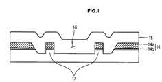
- FIG. 1is process cross-sectional view explaining a method of forming a device isolating layer using a dummy pattern in the related art
- FIG. 2is a dummy rule used for forming the dummy pattern.
- a pad oxide film 14 b and a pad nitride film 14 aare sequentially deposited on a semiconductor substrate 11 . Then, a mask pattern 14 masking a portion of a relatively wide device isolation area is formed on the relatively wide device isolation area, where exposing a device isolation area of the substrate 11 by patterning the pad nitride film 14 a and the pad oxide film 14 b by means of a photolithography and an etching process.
- a trench 16is formed in the device isolation area by etching the substrate 11 using the mask pattern 14 and at the same time, a dummy pattern 17 is formed inside the trench 16 with a relatively wide width.
- the dummy patter 17is arranged spaced from the inner wall of the trench 16 , and has a rectangular photo frame shape, wherein the both sides thereof have a straight profile.
- an oxide film 15is deposited over the substrate 11 so that the trench 16 is buried, and although not shown, the surface thereof is planarized by removing the oxide film 15 so that the surface of the mask pattern 14 is exposed by means of the CMP process and then the mask pattern 14 is removed so that a device isolating layer formed of the oxide film 15 is formed.
- a dummy pattern 40 having the same pattern densityis applied between the chip areas 20 and 30 where a plurality of devices are formed.
- the chip areas 20 and 30 where the devices are formedare not formed having the same pattern density therebetween, but are generally formed so that the pattern density of the first chip area 20 is higher than that of the second chip area 30 .
- the dummy pattern 40 having the same pattern densityis applied without considering the density difference of the chip areas 20 and 30 where the devices are formed, the variation of the pattern within the chip areas 20 and 30 is not reduced, causing the variation of the thickness of the polished surface in the subsequent CMP process.
- the embodimentprovides a method of forming a dummy pattern capable of reducing a pattern density variation within a chip area in a CMP process.
- the method of forming a dummy patterncomprises the step of: for first chip area and second chip area in which devices are formed, forming the dummy pattern formed between a first chip area and a second chip area in a plurality of patterns having various pattern densities.
- the method of forming the dummy patterncomprises the steps of: calculating the distance between a first chip area and a second chip area having different pattern densities; and applying a first dummy pattern rule or a second dummy pattern rule depending on the distance between the first chip area and the second chip area, wherein the first dummy pattern rule or the second dummy pattern rule is formed to have a plurality of dummy patterns having various pattern density.
- FIG. 1is a cross-sectional view of a process explaining a method of forming a device isolating layer using a dummy pattern in the related art, according to one exemplary embodiment.
- FIG. 2is a dummy rule used for forming the dummy pattern, according to one exemplary embodiment.
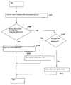
- FIG. 3is a flow chart explaining a method of forming a dummy pattern according to one exemplary embodiment.
- FIG. 4is a view explaining a dummy pattern rule according to one exemplary embodiment.
- FIG. 5is a view explaining a dummy pattern rule according to one exemplary embodiment.
- FIG. 3is a flow chart explaining a method of forming a dummy pattern according to one embodiment.
- the distance A between chip areas where a plurality of devices are formedis calculated (S 101 ).
- the chip areascan be divided into a first chip area having a predetermined pattern density and a second chip area having a relatively lower pattern density as compared to the first chip area.
- a first dummy pattern ruleis applied according to the embodiment (S 105 ).
- a second dummy pattern rule according to a second embodimentis applied (S 109 ).
- a uniform pattern rule having the same pattern densityis applied (S 11 ), wherein the uniform pattern rule represents that the dummy pattern between the chip areas are formed at a uniform density.
- FIG. 4is a dummy rule explaining a dummy pattern rule according to an exemplary embodiment.
- a first chip area 100 and a second chip area 200are formed, and a dummy pattern 300 having various pattern densities is formed between the chip areas 100 and 200 .
- the dummy pattern 300is provided with a third dummy pattern 303 having the average density of the pattern density of the first chip area 100 and the second chip area 200 , first and second dummy patterns 301 and 302 having a lower pattern density than the third dummy pattern 303 , and fourth and fifth dummy patterns 304 and 305 having a higher pattern density than the third dummy pattern 303 .
- the dummy pattern 300when the distance between the first chip area 100 and the second chip area 200 is larger than the first reference distance B, the dummy pattern 300 is formed to have the five partitioned areas as shown, wherein the dummy pattern 300 is formed to have various pattern densities.
- the third dummy pattern 303is approximately formed in the center portion of the distance A between the chip areas, wherein the third dummy pattern 303 is formed at the average density of the pattern density between the first chip area 100 and the second chip area 200 .
- the first dummy pattern 301is formed by about 60% of the pattern density of the third dummy pattern 303
- the second dummy pattern 302is formed by about 80% of the pattern density of the third dummy pattern 303 .
- the fourth dummy pattern 304is formed by about 130% of the pattern density of the third dummy pattern 303
- the fifth dummy pattern 305is formed by about 160% of the pattern density of the third dummy pattern 303 .
- the dummy patternis inserted into the first chip area 100 having high density in the area corresponding to 1 ⁇ 5 from the distance between the chip areas 100 and 200 at the density multiplying the average pattern density d by 60%, and the dummy pattern is inserted into the second chip area 200 having relatively smaller density as compared to the first chip area 100 at the density multiplying the average pattern density d by 160%.
- the dummy patternis again inserted into the area spaced from 1 ⁇ 5 to 2 ⁇ 5 from the first chip area 100 at the density multiplying the average pattern density d by 80%, and the dummy pattern is inserted into the second chip area 200 at the density multiplying the average pattern density d by 130%, and the dummy pattern is finally inserted into the center area at the average pattern density d.
- dummy patternshaving different pattern densities depending on the density of chip area are formed and thus, the thickness variation after being subject to the CMP process is reduced.
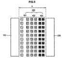
- FIG. 5is a dummy rule explaining a dummy pattern rule according to an exemplary embodiment.
- a first chip area 100 and a second chip area 200 having a plurality of devices formed therein and having different pattern densitiesare formed, and a dummy pattern 400 formed to have various pattern densities is formed between the chip areas 100 and 200 .
- the dummy pattern 400is provided with a second dummy pattern 402 having the average density of the pattern density of the first chip area 100 and the second chip area 200 , a first dummy pattern 401 having a lower pattern density than the second dummy pattern 402 , and a third dummy pattern 403 having a higher pattern density than the second dummy pattern 402 .
- the dummy pattern 400when the distance A between the first chip area 100 and the second chip area 200 is not larger than the first reference distance B but larger than the second reference distance C, the dummy pattern 400 is formed to have the three partitioned areas as shown, wherein the dummy pattern 400 is formed to have various pattern densities.
- the second dummy pattern 402is approximately formed in the center portion of the distance A between the chip areas, wherein the second dummy pattern 402 is formed at the average density of the pattern density between the first chip area 100 and the second chip area 200 .
- the first dummy pattern 401 having relatively lower pattern density than the second dummy pattern 402is formed in the first chip area 100 having relatively higher pattern density as compared to the second chip area 200
- the third dummy pattern 403 having higher pattern density than the second dummy pattern 402is formed in the second chip area 200 .
- the first dummy pattern 401is inserted into the first chip area 100 having high density in the area corresponding to 1 ⁇ 3 from the distance between the chip areas 100 and 200 at the density multiplying the average pattern density d by 60%, and the third dummy pattern 403 is inserted into the second chip area 200 having relatively smaller density as compared to the first chip area 100 at the density multiplying the average pattern density d by 160%.
- the second dummy pattern 402 having the average pattern density d of the chip areas 100 and 200is inserted into between the first dummy pattern 401 and the third dummy pattern 403 .
- the dummy patterns formed between the chip areasare designed in consideration of the pattern density provided in the chip area, having an advantage that the thickness variation within the chip areas after being subject to the CMP process is reduced.
- any reference in this specification to “one embodiment,” “an embodiment,” “example embodiment,” etc.means that a particular feature, structure, or characteristic described in connection with the embodiment is included in at least one embodiment of the invention.
- the appearances of such phrases in various places in the specificationare not necessarily all referring to the same embodiment.
Landscapes
- Engineering & Computer Science (AREA)
- Physics & Mathematics (AREA)
- Condensed Matter Physics & Semiconductors (AREA)
- General Physics & Mathematics (AREA)
- Manufacturing & Machinery (AREA)
- Computer Hardware Design (AREA)
- Microelectronics & Electronic Packaging (AREA)
- Power Engineering (AREA)
- Design And Manufacture Of Integrated Circuits (AREA)
- Preparing Plates And Mask In Photomechanical Process (AREA)
Abstract
Description
Claims (7)
Applications Claiming Priority (4)
| Application Number | Priority Date | Filing Date | Title |
|---|---|---|---|
| KR10-2006-0076189 | 2006-08-11 | ||
| KR1020060076189AKR100789614B1 (en) | 2006-08-11 | 2006-08-11 | Dummy pattern and its formation method |
| KR10-2006-0081965 | 2006-08-28 | ||
| KR1020060081965AKR100789578B1 (en) | 2006-08-28 | 2006-08-28 | Image sensor and its manufacturing method |
Publications (2)
| Publication Number | Publication Date |
|---|---|
| US20080038847A1 US20080038847A1 (en) | 2008-02-14 |
| US7849436B2true US7849436B2 (en) | 2010-12-07 |
Family
ID=39051295
Family Applications (1)
| Application Number | Title | Priority Date | Filing Date |
|---|---|---|---|
| US11/889,384Active2029-05-24US7849436B2 (en) | 2006-08-11 | 2007-08-13 | Method of forming dummy pattern |
Country Status (1)
| Country | Link |
|---|---|
| US (1) | US7849436B2 (en) |
Cited By (3)
| Publication number | Priority date | Publication date | Assignee | Title |
|---|---|---|---|---|
| US20110095374A1 (en)* | 2009-10-23 | 2011-04-28 | Renesas Electronics Corporation | Method, design apparatus, and design program of semiconductor device, and semiconductor device |
| US8719755B2 (en)* | 2012-07-31 | 2014-05-06 | Taiwan Semiconductor Manufacturing Company Limited | Graded dummy insertion |
| US20150161318A1 (en)* | 2013-09-27 | 2015-06-11 | Taiwan Semiconductor Manufacturing Company, Ltd. | Method of making semiconductor device and system for performing the same |
Families Citing this family (5)
| Publication number | Priority date | Publication date | Assignee | Title |
|---|---|---|---|---|
| JP5193582B2 (en) | 2007-12-12 | 2013-05-08 | 株式会社東芝 | Manufacturing method of semiconductor device |
| US8105901B2 (en)* | 2009-07-27 | 2012-01-31 | International Business Machines Corporation | Method for double pattern density |
| DE102013103968B4 (en) | 2012-04-30 | 2023-05-04 | Taiwan Semiconductor Manufacturing Co., Ltd. | Layout of a MOS array edge with density gradient smoothing |
| US9632498B2 (en)* | 2013-03-12 | 2017-04-25 | Taiwan Semiconductor Manufacturing Co., Ltd. | Systems and methods of compensating for filling material losses in electroplating processes |
| KR102565831B1 (en)* | 2019-01-28 | 2023-08-09 | 양쯔 메모리 테크놀로지스 씨오., 엘티디. | Systems and methods for designing dummy patterns |
Citations (14)
| Publication number | Priority date | Publication date | Assignee | Title |
|---|---|---|---|---|
| US5923563A (en)* | 1996-12-20 | 1999-07-13 | International Business Machines Corporation | Variable density fill shape generation |
| US6225697B1 (en)* | 1999-03-29 | 2001-05-01 | Nec Corporation | Semiconductor device and method for manufacturing the same |
| KR20020068419A (en) | 2001-02-21 | 2002-08-27 | 삼성전자 주식회사 | Generation method of data for used in mask including dummy pattern groups having density continuously adjusted in according to density of local design pattern and recording media in which the same recorded |
| US20020157076A1 (en)* | 2001-04-23 | 2002-10-24 | Kazuhiko Asakawa | Fabrication method for a semiconductor device with dummy patterns |
| US20030204832A1 (en)* | 2002-04-26 | 2003-10-30 | Nec Electronics Corporation | Automatic generation method of dummy patterns |
| US20040083438A1 (en)* | 2002-07-05 | 2004-04-29 | Fujitsu Limited | Method, program, and apparatus for designing a semiconductor device |
| US20050097490A1 (en)* | 2003-11-04 | 2005-05-05 | Travis Edward O. | Method of implementing polishing uniformity and modifying layout data |
| US20050235246A1 (en)* | 2002-06-07 | 2005-10-20 | Praesagus, Inc., A Massachusetts Corporation | Use of models in integrated circuit fabrication |
| US20070015365A1 (en)* | 2005-07-14 | 2007-01-18 | Taiwan Semiconductor Manufacturing Co., Ltd. | Method and apparatus for enhanced CMP planarization using surrounded dummy design |
| US7197737B1 (en)* | 2003-12-23 | 2007-03-27 | Cypress Semiconductor Corporation | Techniques for placing dummy features in an integrated circuit based on dielectric pattern density |
| US20070174802A1 (en)* | 2006-01-23 | 2007-07-26 | Shin Jae-Pil | Method of adjusting pattern density |
| US20080034332A1 (en)* | 2006-05-01 | 2008-02-07 | Mentor Graphics Corporation | Optimization Of Geometry Pattern Density |
| US20090024978A1 (en)* | 2007-07-20 | 2009-01-22 | Young-Mi Kim | Semiconductor device mask, method of forming the same and method of manufacturing semiconductor device using the same |
| US20100077367A1 (en)* | 2008-09-25 | 2010-03-25 | Fujitsu Limited | Layout evaluation apparatus and method |
Family Cites Families (34)
| Publication number | Priority date | Publication date | Assignee | Title |
|---|---|---|---|---|
| US5485519A (en)* | 1991-06-07 | 1996-01-16 | Security Dynamics Technologies, Inc. | Enhanced security for a secure token code |
| US5585787A (en)* | 1991-12-09 | 1996-12-17 | Wallerstein; Robert S. | Programmable credit card |
| US5819226A (en)* | 1992-09-08 | 1998-10-06 | Hnc Software Inc. | Fraud detection using predictive modeling |
| US5613012A (en)* | 1994-11-28 | 1997-03-18 | Smarttouch, Llc. | Tokenless identification system for authorization of electronic transactions and electronic transmissions |
| US5802199A (en)* | 1994-11-28 | 1998-09-01 | Smarttouch, Llc | Use sensitive identification system |
| US7613659B1 (en)* | 1994-11-28 | 2009-11-03 | Yt Acquisition Corporation | System and method for processing tokenless biometric electronic transmissions using an electronic rule module clearinghouse |
| US6230148B1 (en)* | 1994-11-28 | 2001-05-08 | Veristar Corporation | Tokenless biometric electric check transaction |
| US20040128249A1 (en)* | 1994-11-28 | 2004-07-01 | Indivos Corporation, A Delaware Corporation | System and method for tokenless biometric electronic scrip |
| US6397198B1 (en)* | 1994-11-28 | 2002-05-28 | Indivos Corporation | Tokenless biometric electronic transactions using an audio signature to identify the transaction processor |
| US6040783A (en)* | 1995-05-08 | 2000-03-21 | Image Data, Llc | System and method for remote, wireless positive identity verification |
| US5696824A (en)* | 1995-06-07 | 1997-12-09 | E-Comm Incorporated | System for detecting unauthorized account access |
| US5995961A (en)* | 1995-11-07 | 1999-11-30 | Lucent Technologies Inc. | Information manifold for query processing |
| US7096198B1 (en)* | 1997-06-16 | 2006-08-22 | Vincent Cuervo | Internet web site program for the purchase, issue and dispensing of debit cards |
| US6041314A (en)* | 1997-12-22 | 2000-03-21 | Davis; Walter Lee | Multiple account portable wireless financial messaging unit |
| US6764001B1 (en)* | 2000-05-30 | 2004-07-20 | Sony Corporation | Electronic money system and transaction method using the same |
| US6529880B1 (en)* | 1999-12-01 | 2003-03-04 | Intermec Ip Corp. | Automatic payment system for a plurality of remote merchants |
| US7163145B2 (en)* | 2000-01-21 | 2007-01-16 | American Express Travel Related Services Co., Inc. | Geographic area multiple service card system |
| US7191150B1 (en)* | 2000-02-01 | 2007-03-13 | Fair Isaac Corporation | Enhancing delinquent debt collection using statistical models of debt historical information and account events |
| US7627531B2 (en)* | 2000-03-07 | 2009-12-01 | American Express Travel Related Services Company, Inc. | System for facilitating a transaction |
| US7383223B1 (en)* | 2000-09-20 | 2008-06-03 | Cashedge, Inc. | Method and apparatus for managing multiple accounts |
| US7606733B2 (en)* | 2000-10-27 | 2009-10-20 | Sandisk Il Ltd. | Account portability for computing |
| US7318049B2 (en)* | 2000-11-17 | 2008-01-08 | Gregory Fx Iannacci | System and method for an automated benefit recognition, acquisition, value exchange, and transaction settlement system using multivariable linear and nonlinear modeling |
| US20020128981A1 (en)* | 2000-12-28 | 2002-09-12 | Kawan Joseph C. | Method and system for facilitating secure customer financial transactions over an open network |
| US6547040B2 (en)* | 2001-04-02 | 2003-04-15 | Ncr Corporation | Self-service checkout system with RFID capability |
| US7463133B2 (en)* | 2001-07-10 | 2008-12-09 | American Express Travel Related Services Company, Inc. | Systems and methods for providing a RF transaction device operable to store multiple distinct calling card accounts |
| US6732919B2 (en)* | 2002-02-19 | 2004-05-11 | Hewlett-Packard Development Company, L.P. | System and method for using a multiple-use credit card |
| US7587756B2 (en)* | 2002-07-09 | 2009-09-08 | American Express Travel Related Services Company, Inc. | Methods and apparatus for a secure proximity integrated circuit card transactions |
| US6805287B2 (en)* | 2002-09-12 | 2004-10-19 | American Express Travel Related Services Company, Inc. | System and method for converting a stored value card to a credit card |
| EP1579298A4 (en)* | 2002-11-05 | 2006-08-09 | Aaron Whiteman | Remote purchasing system and method |
| US6685088B1 (en)* | 2002-12-13 | 2004-02-03 | American Express Travel Related Services Company, Inc. | System and method for selecting an account |
| US20050015332A1 (en)* | 2003-07-18 | 2005-01-20 | Grace Chen | Cashless payment system |
| US7236957B2 (en)* | 2004-02-10 | 2007-06-26 | Bottomline Technologies (De) Inc. | Method for remotely authorizing a payment transaction file over an open network |
| US20050246728A1 (en)* | 2004-04-30 | 2005-11-03 | Hewlett-Packard Development Company, L.P. | Controlling actuator movement |
| US7870071B2 (en)* | 2004-09-08 | 2011-01-11 | American Express Travel Related Services Company, Inc. | Systems, methods, and devices for combined credit card and stored value transaction accounts |
- 2007
- 2007-08-13USUS11/889,384patent/US7849436B2/enactiveActive
Patent Citations (14)
| Publication number | Priority date | Publication date | Assignee | Title |
|---|---|---|---|---|
| US5923563A (en)* | 1996-12-20 | 1999-07-13 | International Business Machines Corporation | Variable density fill shape generation |
| US6225697B1 (en)* | 1999-03-29 | 2001-05-01 | Nec Corporation | Semiconductor device and method for manufacturing the same |
| KR20020068419A (en) | 2001-02-21 | 2002-08-27 | 삼성전자 주식회사 | Generation method of data for used in mask including dummy pattern groups having density continuously adjusted in according to density of local design pattern and recording media in which the same recorded |
| US20020157076A1 (en)* | 2001-04-23 | 2002-10-24 | Kazuhiko Asakawa | Fabrication method for a semiconductor device with dummy patterns |
| US20030204832A1 (en)* | 2002-04-26 | 2003-10-30 | Nec Electronics Corporation | Automatic generation method of dummy patterns |
| US20050235246A1 (en)* | 2002-06-07 | 2005-10-20 | Praesagus, Inc., A Massachusetts Corporation | Use of models in integrated circuit fabrication |
| US20040083438A1 (en)* | 2002-07-05 | 2004-04-29 | Fujitsu Limited | Method, program, and apparatus for designing a semiconductor device |
| US20050097490A1 (en)* | 2003-11-04 | 2005-05-05 | Travis Edward O. | Method of implementing polishing uniformity and modifying layout data |
| US7197737B1 (en)* | 2003-12-23 | 2007-03-27 | Cypress Semiconductor Corporation | Techniques for placing dummy features in an integrated circuit based on dielectric pattern density |
| US20070015365A1 (en)* | 2005-07-14 | 2007-01-18 | Taiwan Semiconductor Manufacturing Co., Ltd. | Method and apparatus for enhanced CMP planarization using surrounded dummy design |
| US20070174802A1 (en)* | 2006-01-23 | 2007-07-26 | Shin Jae-Pil | Method of adjusting pattern density |
| US20080034332A1 (en)* | 2006-05-01 | 2008-02-07 | Mentor Graphics Corporation | Optimization Of Geometry Pattern Density |
| US20090024978A1 (en)* | 2007-07-20 | 2009-01-22 | Young-Mi Kim | Semiconductor device mask, method of forming the same and method of manufacturing semiconductor device using the same |
| US20100077367A1 (en)* | 2008-09-25 | 2010-03-25 | Fujitsu Limited | Layout evaluation apparatus and method |
Non-Patent Citations (1)
| Title |
|---|
| Office Action from Korean Intellectual Property Office dated Aug. 28, 2007 in Korean Application No. 10-2006-0076189. |
Cited By (5)
| Publication number | Priority date | Publication date | Assignee | Title |
|---|---|---|---|---|
| US20110095374A1 (en)* | 2009-10-23 | 2011-04-28 | Renesas Electronics Corporation | Method, design apparatus, and design program of semiconductor device, and semiconductor device |
| US8513033B2 (en)* | 2009-10-23 | 2013-08-20 | Renesas Electronics Corporation | Method, design apparatus, and design program of semiconductor device, and semiconductor device |
| US8719755B2 (en)* | 2012-07-31 | 2014-05-06 | Taiwan Semiconductor Manufacturing Company Limited | Graded dummy insertion |
| US20150161318A1 (en)* | 2013-09-27 | 2015-06-11 | Taiwan Semiconductor Manufacturing Company, Ltd. | Method of making semiconductor device and system for performing the same |
| US9639647B2 (en)* | 2013-09-27 | 2017-05-02 | Taiwan Semiconductor Manufacturing Company, Ltd. | Method of making semiconductor device and system for performing the same |
Also Published As
| Publication number | Publication date |
|---|---|
| US20080038847A1 (en) | 2008-02-14 |
Similar Documents
| Publication | Publication Date | Title |
|---|---|---|
| US7849436B2 (en) | Method of forming dummy pattern | |
| US5902752A (en) | Active layer mask with dummy pattern | |
| KR100789614B1 (en) | Dummy pattern and its formation method | |
| US6475879B2 (en) | Semiconductor wafer, method for processing the same and method for manufacturing semiconductor device | |
| KR100670911B1 (en) | Manufacturing Method of Semiconductor Device | |
| US6518633B2 (en) | Semiconductor device and method for manufacturing the same | |
| US20040033689A1 (en) | Method for defining a dummy pattern around an alignment mark on a wafer | |
| US20030143850A1 (en) | Method for controlling and monitoring a chemical mechanical polishing process | |
| US7645679B2 (en) | Method for forming isolation layer in semiconductor devices | |
| US20060014361A1 (en) | Method for forming device isolation layer of semiconductor device | |
| KR950009889B1 (en) | Manufacturing method of isolation region of semiconductor device using trench method | |
| US6617663B2 (en) | Methods of manufacturing semiconductor devices | |
| US7820504B2 (en) | Method for manufacturing differential isolation structures in a semiconductor electronic device and corresponding structure | |
| US6191041B1 (en) | Method of fabricating semiconductor device | |
| KR19980083839A (en) | Trench isolation method for semiconductor devices | |
| KR100536805B1 (en) | Semiconductor device and method of manufacturing the same | |
| JP2001298081A (en) | Semiconductor device and its manufacturing method | |
| KR100758494B1 (en) | Isolation Regions of Semiconductor Devices and Formation Methods | |
| US6818527B2 (en) | Method of manufacturing semiconductor device with shallow trench isolation | |
| USRE43765E1 (en) | Method for fabricating semiconductor device having trench isolation layer | |
| KR20050012584A (en) | Method for forming isolation layer of semiconductor device | |
| US7429518B2 (en) | Method for forming shallow trench isolation of semiconductor device | |
| US7435642B2 (en) | Method of evaluating the uniformity of the thickness of the polysilicon gate layer | |
| US6482075B1 (en) | Process for planarizing an isolation structure in a substrate | |
| US20070148901A1 (en) | Method for manufacturing a semiconductor device |
Legal Events
| Date | Code | Title | Description |
|---|---|---|---|
| AS | Assignment | Owner name:DONGBU HITEK CO., LTD., KOREA, REPUBLIC OF Free format text:ASSIGNMENT OF ASSIGNORS INTEREST;ASSIGNOR:CHOI, JAE YOUNG;REEL/FRAME:019752/0140 Effective date:20070813 | |
| STCF | Information on status: patent grant | Free format text:PATENTED CASE | |
| FEPP | Fee payment procedure | Free format text:PAYER NUMBER DE-ASSIGNED (ORIGINAL EVENT CODE: RMPN); ENTITY STATUS OF PATENT OWNER: LARGE ENTITY Free format text:PAYOR NUMBER ASSIGNED (ORIGINAL EVENT CODE: ASPN); ENTITY STATUS OF PATENT OWNER: LARGE ENTITY | |
| FPAY | Fee payment | Year of fee payment:4 | |
| AS | Assignment | Owner name:STRATEGIC GLOBAL ADVISORS OF OREGON, INC., OREGON Free format text:ASSIGNMENT OF ASSIGNORS INTEREST;ASSIGNOR:DONGBU HITEK CO., LTD.;REEL/FRAME:035491/0744 Effective date:20150406 | |
| AS | Assignment | Owner name:TESSERA ADVANCED TECHNOLOGIES, INC., CALIFORNIA Free format text:ASSIGNMENT OF ASSIGNORS INTEREST;ASSIGNOR:STRATEGIC GLOBAL ADVISORS OF OREGON, INC.;REEL/FRAME:035620/0771 Effective date:20150422 | |
| AS | Assignment | Owner name:ROYAL BANK OF CANADA, AS COLLATERAL AGENT, CANADA Free format text:SECURITY INTEREST;ASSIGNORS:INVENSAS CORPORATION;TESSERA, INC.;TESSERA ADVANCED TECHNOLOGIES, INC.;AND OTHERS;REEL/FRAME:040797/0001 Effective date:20161201 | |
| MAFP | Maintenance fee payment | Free format text:PAYMENT OF MAINTENANCE FEE, 8TH YEAR, LARGE ENTITY (ORIGINAL EVENT CODE: M1552) Year of fee payment:8 | |
| AS | Assignment | Owner name:BANK OF AMERICA, N.A., NORTH CAROLINA Free format text:SECURITY INTEREST;ASSIGNORS:ROVI SOLUTIONS CORPORATION;ROVI TECHNOLOGIES CORPORATION;ROVI GUIDES, INC.;AND OTHERS;REEL/FRAME:053468/0001 Effective date:20200601 | |
| AS | Assignment | Owner name:INVENSAS BONDING TECHNOLOGIES, INC. (F/K/A ZIPTRONIX, INC.), CALIFORNIA Free format text:RELEASE BY SECURED PARTY;ASSIGNOR:ROYAL BANK OF CANADA;REEL/FRAME:052920/0001 Effective date:20200601 Owner name:TESSERA ADVANCED TECHNOLOGIES, INC, CALIFORNIA Free format text:RELEASE BY SECURED PARTY;ASSIGNOR:ROYAL BANK OF CANADA;REEL/FRAME:052920/0001 Effective date:20200601 Owner name:IBIQUITY DIGITAL CORPORATION, MARYLAND Free format text:RELEASE BY SECURED PARTY;ASSIGNOR:ROYAL BANK OF CANADA;REEL/FRAME:052920/0001 Effective date:20200601 Owner name:DTS, INC., CALIFORNIA Free format text:RELEASE BY SECURED PARTY;ASSIGNOR:ROYAL BANK OF CANADA;REEL/FRAME:052920/0001 Effective date:20200601 Owner name:PHORUS, INC., CALIFORNIA Free format text:RELEASE BY SECURED PARTY;ASSIGNOR:ROYAL BANK OF CANADA;REEL/FRAME:052920/0001 Effective date:20200601 Owner name:TESSERA, INC., CALIFORNIA Free format text:RELEASE BY SECURED PARTY;ASSIGNOR:ROYAL BANK OF CANADA;REEL/FRAME:052920/0001 Effective date:20200601 Owner name:FOTONATION CORPORATION (F/K/A DIGITALOPTICS CORPORATION AND F/K/A DIGITALOPTICS CORPORATION MEMS), CALIFORNIA Free format text:RELEASE BY SECURED PARTY;ASSIGNOR:ROYAL BANK OF CANADA;REEL/FRAME:052920/0001 Effective date:20200601 Owner name:INVENSAS CORPORATION, CALIFORNIA Free format text:RELEASE BY SECURED PARTY;ASSIGNOR:ROYAL BANK OF CANADA;REEL/FRAME:052920/0001 Effective date:20200601 Owner name:DTS LLC, CALIFORNIA Free format text:RELEASE BY SECURED PARTY;ASSIGNOR:ROYAL BANK OF CANADA;REEL/FRAME:052920/0001 Effective date:20200601 | |
| MAFP | Maintenance fee payment | Free format text:PAYMENT OF MAINTENANCE FEE, 12TH YEAR, LARGE ENTITY (ORIGINAL EVENT CODE: M1553); ENTITY STATUS OF PATENT OWNER: LARGE ENTITY Year of fee payment:12 |