US7847358B2 - High performance strained CMOS devices - Google Patents
High performance strained CMOS devicesDownload PDFInfo
- Publication number
- US7847358B2 US7847358B2US11/462,648US46264806AUS7847358B2US 7847358 B2US7847358 B2US 7847358B2US 46264806 AUS46264806 AUS 46264806AUS 7847358 B2US7847358 B2US 7847358B2
- Authority
- US
- United States
- Prior art keywords
- overhang
- current flow
- shallow trench
- trench isolation
- fet device
- Prior art date
- Legal status (The legal status is an assumption and is not a legal conclusion. Google has not performed a legal analysis and makes no representation as to the accuracy of the status listed.)
- Expired - Lifetime, expires
Links
Images


Classifications
- H—ELECTRICITY
- H01—ELECTRIC ELEMENTS
- H01L—SEMICONDUCTOR DEVICES NOT COVERED BY CLASS H10
- H01L21/00—Processes or apparatus adapted for the manufacture or treatment of semiconductor or solid state devices or of parts thereof
- H01L21/70—Manufacture or treatment of devices consisting of a plurality of solid state components formed in or on a common substrate or of parts thereof; Manufacture of integrated circuit devices or of parts thereof
- H01L21/71—Manufacture of specific parts of devices defined in group H01L21/70
- H01L21/76—Making of isolation regions between components
- H—ELECTRICITY
- H10—SEMICONDUCTOR DEVICES; ELECTRIC SOLID-STATE DEVICES NOT OTHERWISE PROVIDED FOR
- H10D—INORGANIC ELECTRIC SEMICONDUCTOR DEVICES
- H10D86/00—Integrated devices formed in or on insulating or conducting substrates, e.g. formed in silicon-on-insulator [SOI] substrates or on stainless steel or glass substrates
- H10D86/01—Manufacture or treatment
- H—ELECTRICITY
- H10—SEMICONDUCTOR DEVICES; ELECTRIC SOLID-STATE DEVICES NOT OTHERWISE PROVIDED FOR
- H10D—INORGANIC ELECTRIC SEMICONDUCTOR DEVICES
- H10D30/00—Field-effect transistors [FET]
- H10D30/01—Manufacture or treatment
- H10D30/021—Manufacture or treatment of FETs having insulated gates [IGFET]
- H10D30/0223—Manufacture or treatment of FETs having insulated gates [IGFET] having source and drain regions or source and drain extensions self-aligned to sides of the gate
- H—ELECTRICITY
- H10—SEMICONDUCTOR DEVICES; ELECTRIC SOLID-STATE DEVICES NOT OTHERWISE PROVIDED FOR
- H10D—INORGANIC ELECTRIC SEMICONDUCTOR DEVICES
- H10D30/00—Field-effect transistors [FET]
- H10D30/60—Insulated-gate field-effect transistors [IGFET]
- H10D30/791—Arrangements for exerting mechanical stress on the crystal lattice of the channel regions
- H10D30/795—Arrangements for exerting mechanical stress on the crystal lattice of the channel regions being in lateral device isolation regions, e.g. STI
- H—ELECTRICITY
- H10—SEMICONDUCTOR DEVICES; ELECTRIC SOLID-STATE DEVICES NOT OTHERWISE PROVIDED FOR
- H10D—INORGANIC ELECTRIC SEMICONDUCTOR DEVICES
- H10D84/00—Integrated devices formed in or on semiconductor substrates that comprise only semiconducting layers, e.g. on Si wafers or on GaAs-on-Si wafers
- H10D84/01—Manufacture or treatment
- H10D84/0123—Integrating together multiple components covered by H10D12/00 or H10D30/00, e.g. integrating multiple IGBTs
- H10D84/0126—Integrating together multiple components covered by H10D12/00 or H10D30/00, e.g. integrating multiple IGBTs the components including insulated gates, e.g. IGFETs
- H10D84/0165—Integrating together multiple components covered by H10D12/00 or H10D30/00, e.g. integrating multiple IGBTs the components including insulated gates, e.g. IGFETs the components including complementary IGFETs, e.g. CMOS devices
- H10D84/0167—Manufacturing their channels
- H—ELECTRICITY
- H10—SEMICONDUCTOR DEVICES; ELECTRIC SOLID-STATE DEVICES NOT OTHERWISE PROVIDED FOR
- H10D—INORGANIC ELECTRIC SEMICONDUCTOR DEVICES
- H10D84/00—Integrated devices formed in or on semiconductor substrates that comprise only semiconducting layers, e.g. on Si wafers or on GaAs-on-Si wafers
- H10D84/01—Manufacture or treatment
- H10D84/0123—Integrating together multiple components covered by H10D12/00 or H10D30/00, e.g. integrating multiple IGBTs
- H10D84/0126—Integrating together multiple components covered by H10D12/00 or H10D30/00, e.g. integrating multiple IGBTs the components including insulated gates, e.g. IGFETs
- H10D84/0165—Integrating together multiple components covered by H10D12/00 or H10D30/00, e.g. integrating multiple IGBTs the components including insulated gates, e.g. IGFETs the components including complementary IGFETs, e.g. CMOS devices
- H10D84/0188—Manufacturing their isolation regions
- H—ELECTRICITY
- H10—SEMICONDUCTOR DEVICES; ELECTRIC SOLID-STATE DEVICES NOT OTHERWISE PROVIDED FOR
- H10D—INORGANIC ELECTRIC SEMICONDUCTOR DEVICES
- H10D84/00—Integrated devices formed in or on semiconductor substrates that comprise only semiconducting layers, e.g. on Si wafers or on GaAs-on-Si wafers
- H10D84/01—Manufacture or treatment
- H10D84/02—Manufacture or treatment characterised by using material-based technologies
- H10D84/03—Manufacture or treatment characterised by using material-based technologies using Group IV technology, e.g. silicon technology or silicon-carbide [SiC] technology
- H10D84/038—Manufacture or treatment characterised by using material-based technologies using Group IV technology, e.g. silicon technology or silicon-carbide [SiC] technology using silicon technology, e.g. SiGe
- H—ELECTRICITY
- H10—SEMICONDUCTOR DEVICES; ELECTRIC SOLID-STATE DEVICES NOT OTHERWISE PROVIDED FOR
- H10D—INORGANIC ELECTRIC SEMICONDUCTOR DEVICES
- H10D30/00—Field-effect transistors [FET]
- H10D30/60—Insulated-gate field-effect transistors [IGFET]
Definitions
- the inventiongenerally relates to a semiconductor device and method of manufacture and, more particularly, to a complementary metal-oxide-semiconductor (CMOS) device that includes shallow trench isolations (STI) over-hanging interfaces thus preventing oxidation induced compressive stresses in the device.
- CMOScomplementary metal-oxide-semiconductor
- CMOS devicesmay be fabricated using various process techniques.
- One methodentails fabricating strained Silicon (Si) layers on relaxed Silicon Germanium (SiGe) layers. As the Germanium (Ge) concentration increases, strain in the Si lattice increases. This is significant because such strain affects performance (e.g., electron and hole mobility). While strain may improve electron mobility in n-channel field effect transistors (nFETs), performance improvement (i.e., enhancement of hole mobility) in p-channel field effect transistors (pFETs) poses a greater challenge. Hole mobility in a pFET initially exhibits a slight degradation at low amount of tensile strain, but increases linearly with higher strain.
- STIshallow trench isolation
- Si located adjacent to the vertical portion of an STIis susceptible to oxidation induced stress.
- the Simay become oxidized during gate oxidation or reoxidation of a gate stack.
- the oxidized portionmay exhibit significantly increased thickness due to the use of multiple gate oxidations, which is common in fabricating high performance logic circuits.
- the increased thicknessinduces stress in the silicon active area, which can affect performance, such as adversely by decreasing nFET electron mobility
- the inventionis directed to overcoming one or more of the problems as set forth above.
- a semiconductor structureis formed on a substrate, comprising at least one shallow trench isolation having at least one overhang selectively configured to prevent oxidation induced stress in a determined portion of the substrate.
- a semiconductor structureis formed on a substrate.
- the structureincludes a first field effect transistor having a source, a drain, a gate, and a direction of current flow from the source to the drain.
- the structurealso includes a first shallow trench isolation for the first field effect transistor.
- the first shallow trench isolationhas at least one overhang configured to prevent oxidation induced stress in a direction parallel to the direction of current flow for the first field effect transistor.
- a process of forming a semiconductor structureentails forming a first shallow trench isolation.
- the shallow trench isolationhas at least one overhang configured to prevent oxidation induced stress in a first determined direction.
- a structureis formed comprising a silicon layer, a silicon dioxide layer on the silicon layer, and a silicon nitride layer on the silicon dioxide layer.
- a portion of the silicon nitride layer, the silicon dioxide layer and the silicon substrateis etched to form a trench.
- Side-wall portions of the silicon nitride layer in the trenchare etched to create a recession of the silicon nitride layer relative to the trench.
- a shallow trench isolationis formed in the trench, which in embodiments has an overhang.
- FIG. 1shows a silicon substrate with oxide and nitride layers for use in accordance with an exemplary implementation of the invention
- FIG. 2shows a silicon substrate with patterned photoresist images on a nitride surface for use in accordance with an exemplary implementation of the invention
- FIG. 3shows an etched semiconductor structure with trenches for use in accordance with an exemplary implementation of the invention
- FIG. 4shows a semiconductor structure having shallow trench isolations for use in accordance with an exemplary implementation of the invention
- FIG. 5shows a semiconductor structure having shallow trench isolations with overhangs for use in accordance with an exemplary implementation of the invention
- FIG. 6shows a semiconductor structure having shallow trench isolations with overhangs after removal of a nitride layer and reduction of oxide thickness
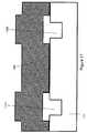
- FIG. 7shows a top plan view of an active device (e.g., an nFET or pFET) surrounded by a shallow trench isolation;
- an active devicee.g., an nFET or pFET
- FIG. 8shows a pFET device in accordance with an exemplary embodiment of the invention
- FIG. 9shows an nFET device in accordance with an exemplary embodiment of the invention.
- FIG. 10shows a parallel-to-gate view of an exemplary pFET device having STI overhangs in the direction transverse to current flow
- FIG. 11shows a parallel-to-gate view of an nFET device having STI overhangs in the direction transverse to current flow.
- the inventionemploys a silicon nitride (Si 3 N 4 ) pull-back process in combination with a mask used to prevent the Si 3 N 4 pull-back from being executed in the longitudinal components of some or all pFET devices.
- the resulting semiconductor structurehas overhang structures (referred to herein as overhang, SiO 2 overhang, and STI overhang) present for nFET devices in the directions of and transverse to current flow.
- overhangSiO 2 overhang
- STI overhangsilicon dioxide
- no silicon dioxide (SiO 2 ) overhangis present in the direction parallel to the direction of current flow for pFET devices.
- the structurehas SiO 2 overhangs in the direction transverse to current flow for pFET devices to avoid performance degradation from compressive stresses.
- the overhang structuresprevent oxidation by blocking access to underlying Si. Without an overhang, Si at the vertical Si—SiO 2 interface adjacent to the shallow trench isolation would be susceptible to oxidation and attendant volume expansion, especially during gate oxidation and reoxidation process steps. It is believed that the resulting semi-conductor structure enables pFET performance improvement with little or no nFET performance degradation. Additionally, the overhang structure is detectable using standard failure analysis techniques such as scanning electron microscopy (SEM).
- SEMscanning electron microscopy
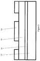
- a silicon substrate 110a pad silicon dioxide (SiO 2 ) layer 120 and a pad silicon nitride (Si 3 N 4 ) layer 130 are provided.
- the silicon substratemay be a silicon wafer, an epitaxial layer formed on a silicon wafer or a silicon-on-insulator (SOI) substrate.
- the silicon dioxide layer 120may be about 2 nm to 70 nm thick, and may be deposited or grown on the wafer.
- the silicon dioxide layer 120may be formed by thermal oxidation or by low pressure chemical vapor deposition (LPCVD).
- LPCVDlow pressure chemical vapor deposition
- the silicon nitride layer 130in the range of about 10 to 400 nm, may be deposited by LPCVD.
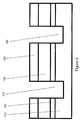
- a photolithography processmay then be carried out to pattern photoresist images 210 over the silicon nitride layer 130 .
- the inverse patternmay then be etched using a dry or wet etch process (e.g., by reactive ion etching using the patterned photoresist as a mask) to form trench structures, as is well known in the art.
- the dry or wet etch processmay be carried out to etch the silicon nitride 130 , silicon dioxide 120 and some amount of the silicon substrate 110 not covered by the photoresist image 210 .
- trenches 310 and 320are formed through layers 110 , 120 and 130 .
- the trenches 310 and 320may be filled with SiO 2 , such as by depositing SiO 2 over the surface of the substrate using, for example, a chemical vapor deposition (CVD) or plasma CVD process.
- the deposited SiO 2may then be planarized using, for example, reactive ion etching (RIE), chemical mechanical polishing, or a combination thereof.
- RIEreactive ion etching
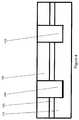
- shallow trench isolations 410 and 420are formed. These shallow trench isolations 410 and 420 do not exhibit overhang.
- portions of the silicon nitride layer 130are etched, causing them to recede or pull-back relative to the side walls of the trench, as shown in FIG. 5
- the silicon nitride layer 130may be etched (i.e., “pulled back”), for example, by introducing an etchant such as a glycerated buffered hydrofluoric acid in trenches 310 and 320 prior to oxide deposition and chemical mechanical polishing.
- an etchantsuch as a glycerated buffered hydrofluoric acid
- the amountshould be sufficient to enable formation of an overhang that is sufficient to prevent oxidation in a determined portion of the device.
- the overhangshould not interfere with other structures on the device.
- an overhang that extends beyond the STI-substrate interface by 0.01 ⁇ m to 0.5 ⁇ m (microns)should be sufficient to prevent oxidation without causing interference.
- a photoresist or hardmaskmay be selectively applied to prevent etchant (e.g., glycerated buffered hydrofluoric acid) from under-cutting determined areas. Areas protected by a photoresist or hardmask would not exhibit pull-back required for the formation of overhangs.
- etchante.g., glycerated buffered hydrofluoric acid
- Processes for depositing and patterning a hardmask or photoresistare known in the art of semiconductor fabrication. The hardmask or photoresist may then be removed in subsequent processing steps.
- the structures 510 and 520are formed, as shown in FIG. 5 .
- Portions of SiO 2 122 - 128 ( FIG. 6 ) from the oxide layer 120may remain after trench formation and pull-back.
- these portions 122 - 128are comprised of the same material as the T-shaped structures 510 and 520 , the portions are not distinguished from the T-shaped structures in subsequent Figures.
- the shallow trench isolation structures of FIG. 5form T-shapes or a stepped portion 510 a and 520 a , respectively (e.g., a narrow portion embedded in the layers 110 and 120 ) thus forming the overhang over layer 120 .
- the top horizontal portions or stepped portions 510 a and 520 a , respectively, of these shallow trench isolation structures 510 and 520now overhang the vertical Si—SiO 2 interfaces 620 626 and therefore inhibit oxidation of the Si portions of the inter-faces. Consequently, oxidation induced compression may be prevented in the channel region.
- a CMOS circuit comprising an nFETmay have STI structures with overhangs in the direction parallel to the direction of current flow and in the direction transverse to current flow to prevent oxidation of Si along the Si—SiO 2 interfaces.
- a pFET devicemay have an overhang in the transverse direction, but no overhang in the direction parallel to the direction of current flow in accordance with FIG. 4 .
- the silicon nitride layer 130( FIG. 5 ) is removed by hot phosphoric acid, for example.
- well implants to form source and drain regionswhich are used in a conventional process flow, are carried out.
- a timed hydrofluoric acid etchmay then be used to prepare the silicon surface for gate oxidation.
- the oxide layers 120 , 510 and 520are reduced in thickness by such etching.
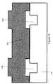
- FIG. 7provides a top plan view of a shallow trench isolation 710 surrounding an active device comprised of a gate electrode 720 and an active silicon area 730 .
- the shallow trench isolation 710includes two sides 740 and 750 parallel to the direction of current flow and two sides 760 and 770 transverse to the direction of current flow.
- the sidesmay have STI overhangs or may be devoid of overhangs.
- An overhang on side 740 and/or 750which are sides parallel to the direction of current flow, is an overhang parallel to the direction of current flow.
- An overhang on side 760 and/or 770which are sides transverse to the direction of current flow, is an overhang transverse to the direction of current flow.
- the exemplary deviceincludes a shallow trench isolation with sides 410 and 420 without overhangs in the direction parallel to the direction of current flow. STI overhangs may be provided in the transverse direction for pFETs.
- the active devicemay be comprised of conventional gate dielectric 845 , a gate electrode 830 and side-wall spacers 820 and 835 all formed in a conventional manner. Silicide (e.g., TiSi 2 , TaSi 2 or MoSi 2 ) 810 and 840 for source and drain contacts may also be provided.
- the deviceincludes a shallow trench isolation with sides 510 and 520 having overhangs in the direction parallel to the direction of current flow.
- the active devicemay be comprised of conventional gate dielectric 945 , a gate electrode 930 and sidewall spacers 920 and 940 .
- Silicidee.g., TiSi 2 , TaSi 2 or MoSi 2
- the overhangsprevent oxidation induced bird's beak formation near the vertical Si—SiO 2 interface. Thus, oxidation induced compressive stresses, which would degrade electron mobility of the nFET, are avoided.
- a cross-sectional parallel-to-gate 930 view of a pFET device in accordance with an exemplary embodiment of the inventionshows STI overhangs 1010 and 1020 in the direction transverse to current flow.
- the STI overhangs 1010 and 1020prevent oxidation induced compressive stress formations (e.g., bird's beak formations) in the transverse direction, thus preventing a degradation of hole mobility.
- the STI overhangs in the transverse directionmay be formed using a technique (e.g., a silicon nitride pullback process), as used to form STI overhangs in the direction parallel to the direction of current flow.
- FIG. 11provides a cross-sectional parallel-to-gate 830 view of an exemplary nFET device which shows STI overhangs 1110 and 1120 in the direction transverse to current flow.
- the STI overhangs 1110 and 1120prevent oxidation induced compressive stress formations in the transverse direction, thus preventing a degradation of electron mobility.
- the STI overhangs in the transverse directionmay be formed using a technique (e.g., a silicon nitride pullback process) as used to form STI overhangs in the direction parallel to the direction of current flow.
- Stress effectsare inversely related to distance from the active device. The closer the source of oxidation induced compressive stresses is to an active device, the greater the impact on performance. Conversely, the greater the distance between a field effect transistor gate and a source of oxidation induced compressive stress (e.g., a bird's beak formation), the less appreciable the influence on performance. Furthermore, sources of oxidation induced compressive stress (e.g., bird's beak formations) that are more than a determined distance from a determined active structure (e.g., the nearest edge of a transistor gate) may not appreciably affect performance (e.g., electron or hole mobility) for that structure.
- performancee.g., electron or hole mobility
- STI overhangsmay be implemented if the distance between the STI and the determined structure is less than or equal to the determined distance.
- the determined distancemay vary depending upon factors that may influence the magnitude of stress induced. Such factors may include, by way of example, thermal mismatch between the isolation, dielectric and silicon substrate; intrinsic stress of a nitride mask; as well as fabrication steps and conditions. Because a stress source beyond that distance may not have an appreciable effect on performance, in such a case formation of STI overhangs may not be warranted for stress reduction purposes.
- a distance of 5.0.mu. (microns) or greater from a nearest edge of an nFET or pFET gatemay be sufficient to avoid performance degradation.
- STI overhang structures in accordance with an exemplary implementationmay therefore be selectively configured to prevent bird's beak formations where compressive stresses caused by such formations would degrade performance.
- STI overhangsmay be provided in both the directions parallel and transverse to the direction of current flow for nFETs; a pFET may have an STI overhang in the transverse direction, but should not have an overhang, in embodiments, in the parallel direction.
- the selective configurationmay further take into account the distance between an STI and the active device (e.g., the distance between an STI and a nearby gate). If the distance prevents bird's beak formations adjacent to the STI from having any appreciable effects on performance, then overhangs may be omitted.
Landscapes
- Engineering & Computer Science (AREA)
- Physics & Mathematics (AREA)
- Condensed Matter Physics & Semiconductors (AREA)
- General Physics & Mathematics (AREA)
- Manufacturing & Machinery (AREA)
- Computer Hardware Design (AREA)
- Microelectronics & Electronic Packaging (AREA)
- Power Engineering (AREA)
- Insulated Gate Type Field-Effect Transistor (AREA)
- Element Separation (AREA)
- Metal-Oxide And Bipolar Metal-Oxide Semiconductor Integrated Circuits (AREA)
- Thin Film Transistor (AREA)
Abstract
Description
Claims (14)
Priority Applications (1)
| Application Number | Priority Date | Filing Date | Title |
|---|---|---|---|
| US11/462,648US7847358B2 (en) | 2003-10-16 | 2006-08-04 | High performance strained CMOS devices |
Applications Claiming Priority (2)
| Application Number | Priority Date | Filing Date | Title |
|---|---|---|---|
| US10/605,672US7119403B2 (en) | 2003-10-16 | 2003-10-16 | High performance strained CMOS devices |
| US11/462,648US7847358B2 (en) | 2003-10-16 | 2006-08-04 | High performance strained CMOS devices |
Related Parent Applications (1)
| Application Number | Title | Priority Date | Filing Date |
|---|---|---|---|
| US10/605,672ContinuationUS7119403B2 (en) | 2003-10-16 | 2003-10-16 | High performance strained CMOS devices |
Publications (2)
| Publication Number | Publication Date |
|---|---|
| US20060270136A1 US20060270136A1 (en) | 2006-11-30 |
| US7847358B2true US7847358B2 (en) | 2010-12-07 |
Family
ID=34465414
Family Applications (3)
| Application Number | Title | Priority Date | Filing Date |
|---|---|---|---|
| US10/605,672Expired - LifetimeUS7119403B2 (en) | 2003-10-16 | 2003-10-16 | High performance strained CMOS devices |
| US11/060,784Expired - Fee RelatedUS7205207B2 (en) | 2003-10-16 | 2005-02-18 | High performance strained CMOS devices |
| US11/462,648Expired - LifetimeUS7847358B2 (en) | 2003-10-16 | 2006-08-04 | High performance strained CMOS devices |
Family Applications Before (2)
| Application Number | Title | Priority Date | Filing Date |
|---|---|---|---|
| US10/605,672Expired - LifetimeUS7119403B2 (en) | 2003-10-16 | 2003-10-16 | High performance strained CMOS devices |
| US11/060,784Expired - Fee RelatedUS7205207B2 (en) | 2003-10-16 | 2005-02-18 | High performance strained CMOS devices |
Country Status (7)
| Country | Link |
|---|---|
| US (3) | US7119403B2 (en) |
| EP (1) | EP1678753B1 (en) |
| JP (1) | JP4953818B2 (en) |
| KR (1) | KR100843653B1 (en) |
| CN (1) | CN100530589C (en) |
| TW (1) | TWI331790B (en) |
| WO (1) | WO2005038875A2 (en) |
Cited By (2)
| Publication number | Priority date | Publication date | Assignee | Title |
|---|---|---|---|---|
| US20160247004A1 (en)* | 2009-10-14 | 2016-08-25 | Xyleco, Inc. | Marking paper products |
| US10410453B2 (en) | 2014-07-08 | 2019-09-10 | Xyleco, Inc. | Marking plastic-based products |
Families Citing this family (50)
| Publication number | Priority date | Publication date | Assignee | Title |
|---|---|---|---|---|
| US7410846B2 (en)* | 2003-09-09 | 2008-08-12 | International Business Machines Corporation | Method for reduced N+ diffusion in strained Si on SiGe substrate |
| US6887751B2 (en) | 2003-09-12 | 2005-05-03 | International Business Machines Corporation | MOSFET performance improvement using deformation in SOI structure |
| US7144767B2 (en)* | 2003-09-23 | 2006-12-05 | International Business Machines Corporation | NFETs using gate induced stress modulation |
| US6872641B1 (en)* | 2003-09-23 | 2005-03-29 | International Business Machines Corporation | Strained silicon on relaxed sige film with uniform misfit dislocation density |
| US7119403B2 (en)* | 2003-10-16 | 2006-10-10 | International Business Machines Corporation | High performance strained CMOS devices |
| US7037770B2 (en)* | 2003-10-20 | 2006-05-02 | International Business Machines Corporation | Method of manufacturing strained dislocation-free channels for CMOS |
| US7303949B2 (en) | 2003-10-20 | 2007-12-04 | International Business Machines Corporation | High performance stress-enhanced MOSFETs using Si:C and SiGe epitaxial source/drain and method of manufacture |
| US7129126B2 (en)* | 2003-11-05 | 2006-10-31 | International Business Machines Corporation | Method and structure for forming strained Si for CMOS devices |
| US7015082B2 (en)* | 2003-11-06 | 2006-03-21 | International Business Machines Corporation | High mobility CMOS circuits |
| US7029964B2 (en) | 2003-11-13 | 2006-04-18 | International Business Machines Corporation | Method of manufacturing a strained silicon on a SiGe on SOI substrate |
| US7122849B2 (en) | 2003-11-14 | 2006-10-17 | International Business Machines Corporation | Stressed semiconductor device structures having granular semiconductor material |
| US7247534B2 (en) | 2003-11-19 | 2007-07-24 | International Business Machines Corporation | Silicon device on Si:C-OI and SGOI and method of manufacture |
| US7198995B2 (en)* | 2003-12-12 | 2007-04-03 | International Business Machines Corporation | Strained finFETs and method of manufacture |
| US7247912B2 (en)* | 2004-01-05 | 2007-07-24 | International Business Machines Corporation | Structures and methods for making strained MOSFETs |
| US7381609B2 (en)* | 2004-01-16 | 2008-06-03 | International Business Machines Corporation | Method and structure for controlling stress in a transistor channel |
| US7118999B2 (en)* | 2004-01-16 | 2006-10-10 | International Business Machines Corporation | Method and apparatus to increase strain effect in a transistor channel |
| US7202132B2 (en) | 2004-01-16 | 2007-04-10 | International Business Machines Corporation | Protecting silicon germanium sidewall with silicon for strained silicon/silicon germanium MOSFETs |
| US7205206B2 (en)* | 2004-03-03 | 2007-04-17 | International Business Machines Corporation | Method of fabricating mobility enhanced CMOS devices |
| US7223994B2 (en)* | 2004-06-03 | 2007-05-29 | International Business Machines Corporation | Strained Si on multiple materials for bulk or SOI substrates |
| TWI463526B (en)* | 2004-06-24 | 2014-12-01 | Ibm | Method for improving stress-induced CMOS components and components prepared by the method |
| US7288443B2 (en)* | 2004-06-29 | 2007-10-30 | International Business Machines Corporation | Structures and methods for manufacturing p-type MOSFET with graded embedded silicon-germanium source-drain and/or extension |
| US7384829B2 (en) | 2004-07-23 | 2008-06-10 | International Business Machines Corporation | Patterned strained semiconductor substrate and device |
| US7173312B2 (en)* | 2004-12-15 | 2007-02-06 | International Business Machines Corporation | Structure and method to generate local mechanical gate stress for MOSFET channel mobility modification |
| US20060160317A1 (en)* | 2005-01-18 | 2006-07-20 | International Business Machines Corporation | Structure and method to enhance stress in a channel of cmos devices using a thin gate |
| US7256081B2 (en)* | 2005-02-01 | 2007-08-14 | International Business Machines Corporation | Structure and method to induce strain in a semiconductor device channel with stressed film under the gate |
| US7224033B2 (en) | 2005-02-15 | 2007-05-29 | International Business Machines Corporation | Structure and method for manufacturing strained FINFET |
| US7545004B2 (en)* | 2005-04-12 | 2009-06-09 | International Business Machines Corporation | Method and structure for forming strained devices |
| US7655511B2 (en) | 2005-11-03 | 2010-02-02 | International Business Machines Corporation | Gate electrode stress control for finFET performance enhancement |
| US7564081B2 (en) | 2005-11-30 | 2009-07-21 | International Business Machines Corporation | finFET structure with multiply stressed gate electrode |
| US7635620B2 (en) | 2006-01-10 | 2009-12-22 | International Business Machines Corporation | Semiconductor device structure having enhanced performance FET device |
| US20070158743A1 (en)* | 2006-01-11 | 2007-07-12 | International Business Machines Corporation | Thin silicon single diffusion field effect transistor for enhanced drive performance with stress film liners |
| US7691698B2 (en) | 2006-02-21 | 2010-04-06 | International Business Machines Corporation | Pseudomorphic Si/SiGe/Si body device with embedded SiGe source/drain |
| US8035168B2 (en)* | 2006-02-27 | 2011-10-11 | Synopsys, Inc. | Elevation of transistor channels to reduce impact of shallow trench isolation on transistor performance |
| US7521307B2 (en)* | 2006-04-28 | 2009-04-21 | International Business Machines Corporation | CMOS structures and methods using self-aligned dual stressed layers |
| US7608489B2 (en)* | 2006-04-28 | 2009-10-27 | International Business Machines Corporation | High performance stress-enhance MOSFET and method of manufacture |
| US7615418B2 (en)* | 2006-04-28 | 2009-11-10 | International Business Machines Corporation | High performance stress-enhance MOSFET and method of manufacture |
| US8853746B2 (en) | 2006-06-29 | 2014-10-07 | International Business Machines Corporation | CMOS devices with stressed channel regions, and methods for fabricating the same |
| US7790540B2 (en) | 2006-08-25 | 2010-09-07 | International Business Machines Corporation | Structure and method to use low k stress liner to reduce parasitic capacitance |
| US7462522B2 (en)* | 2006-08-30 | 2008-12-09 | International Business Machines Corporation | Method and structure for improving device performance variation in dual stress liner technology |
| US8754446B2 (en) | 2006-08-30 | 2014-06-17 | International Business Machines Corporation | Semiconductor structure having undercut-gate-oxide gate stack enclosed by protective barrier material |
| US20080237733A1 (en)* | 2007-03-27 | 2008-10-02 | International Business Machines Corporation | Structure and method to enhance channel stress by using optimized sti stress and nitride capping layer stress |
| US7615435B2 (en)* | 2007-07-31 | 2009-11-10 | International Business Machines Corporation | Semiconductor device and method of manufacture |
| US8115254B2 (en) | 2007-09-25 | 2012-02-14 | International Business Machines Corporation | Semiconductor-on-insulator structures including a trench containing an insulator stressor plug and method of fabricating same |
| US8492846B2 (en) | 2007-11-15 | 2013-07-23 | International Business Machines Corporation | Stress-generating shallow trench isolation structure having dual composition |
| US7858482B2 (en)* | 2008-03-31 | 2010-12-28 | Freescale Semiconductor, Inc. | Method of forming a semiconductor device using stress memorization |
| US8598006B2 (en)* | 2010-03-16 | 2013-12-03 | International Business Machines Corporation | Strain preserving ion implantation methods |
| US8623713B2 (en) | 2011-09-15 | 2014-01-07 | International Business Machines Corporation | Trench isolation structure |
| US20140264444A1 (en)* | 2013-03-13 | 2014-09-18 | International Business Machines Corporation | Stress-enhancing selective epitaxial deposition of embedded source and drain regions |
| US11022886B2 (en)* | 2017-05-17 | 2021-06-01 | Taiwan Semiconductor Manufacturing Co,, Ltd. | Bottom-up material formation for planarization |
| US20230402504A1 (en)* | 2022-06-09 | 2023-12-14 | Invention And Collaboration Laboratory Pte. Ltd. | Metal-oxide-semiconductor field-effect transistor structure with low leakage current and reserved gate length |
Citations (113)
| Publication number | Priority date | Publication date | Assignee | Title |
|---|---|---|---|---|
| US3602841A (en) | 1970-06-18 | 1971-08-31 | Ibm | High frequency bulk semiconductor amplifiers and oscillators |
| US4665415A (en) | 1985-04-24 | 1987-05-12 | International Business Machines Corporation | Semiconductor device with hole conduction via strained lattice |
| US4853076A (en) | 1983-12-29 | 1989-08-01 | Massachusetts Institute Of Technology | Semiconductor thin films |
| US4855245A (en) | 1985-09-13 | 1989-08-08 | Siemens Aktiengesellschaft | Method of manufacturing integrated circuit containing bipolar and complementary MOS transistors on a common substrate |
| US4952524A (en) | 1989-05-05 | 1990-08-28 | At&T Bell Laboratories | Semiconductor device manufacture including trench formation |
| US4958213A (en) | 1987-12-07 | 1990-09-18 | Texas Instruments Incorporated | Method for forming a transistor base region under thick oxide |
| US5006913A (en) | 1988-11-05 | 1991-04-09 | Mitsubishi Denki Kabushiki Kaisha | Stacked type semiconductor device |
| US5060030A (en) | 1990-07-18 | 1991-10-22 | Raytheon Company | Pseudomorphic HEMT having strained compensation layer |
| US5081513A (en) | 1991-02-28 | 1992-01-14 | Xerox Corporation | Electronic device with recovery layer proximate to active layer |
| US5108843A (en) | 1988-11-30 | 1992-04-28 | Ricoh Company, Ltd. | Thin film semiconductor and process for producing the same |
| US5134085A (en) | 1991-11-21 | 1992-07-28 | Micron Technology, Inc. | Reduced-mask, split-polysilicon CMOS process, incorporating stacked-capacitor cells, for fabricating multi-megabit dynamic random access memories |
| US5310446A (en) | 1990-01-10 | 1994-05-10 | Ricoh Company, Ltd. | Method for producing semiconductor film |
| US5354695A (en) | 1992-04-08 | 1994-10-11 | Leedy Glenn J | Membrane dielectric isolation IC fabrication |
| US5371399A (en) | 1991-06-14 | 1994-12-06 | International Business Machines Corporation | Compound semiconductor having metallic inclusions and devices fabricated therefrom |
| US5391510A (en) | 1992-02-28 | 1995-02-21 | International Business Machines Corporation | Formation of self-aligned metal gate FETs using a benignant removable gate material during high temperature steps |
| US5459346A (en) | 1988-06-28 | 1995-10-17 | Ricoh Co., Ltd. | Semiconductor substrate with electrical contact in groove |
| US5557122A (en) | 1995-05-12 | 1996-09-17 | Alliance Semiconductors Corporation | Semiconductor electrode having improved grain structure and oxide growth properties |
| US5561302A (en) | 1994-09-26 | 1996-10-01 | Motorola, Inc. | Enhanced mobility MOSFET device and method |
| US5670798A (en) | 1995-03-29 | 1997-09-23 | North Carolina State University | Integrated heterostructures of Group III-V nitride semiconductor materials including epitaxial ohmic contact non-nitride buffer layer and methods of fabricating same |
| US5679965A (en) | 1995-03-29 | 1997-10-21 | North Carolina State University | Integrated heterostructures of Group III-V nitride semiconductor materials including epitaxial ohmic contact, non-nitride buffer layer and methods of fabricating same |
| US5834358A (en) | 1996-11-12 | 1998-11-10 | Micron Technology, Inc. | Isolation regions and methods of forming isolation regions |
| US5861651A (en) | 1997-02-28 | 1999-01-19 | Lucent Technologies Inc. | Field effect devices and capacitors with improved thin film dielectrics and method for making same |
| US5880040A (en) | 1996-04-15 | 1999-03-09 | Macronix International Co., Ltd. | Gate dielectric based on oxynitride grown in N2 O and annealed in NO |
| KR100213196B1 (en) | 1996-03-15 | 1999-08-02 | 윤종용 | Trench device separation |
| US5940736A (en) | 1997-03-11 | 1999-08-17 | Lucent Technologies Inc. | Method for forming a high quality ultrathin gate oxide layer |
| US5953621A (en) | 1997-03-25 | 1999-09-14 | Micron Technology Inc. | Method for forming a self-aligned isolation trench |
| US5960297A (en) | 1997-07-02 | 1999-09-28 | Kabushiki Kaisha Toshiba | Shallow trench isolation structure and method of forming the same |
| US5963819A (en) | 1998-01-26 | 1999-10-05 | United Silicon Incorporated | Method of fabricating shallow trench isolation |
| US5976948A (en) | 1998-02-19 | 1999-11-02 | Advanced Micro Devices | Process for forming an isolation region with trench cap |
| US5981356A (en) | 1997-07-28 | 1999-11-09 | Integrated Device Technology, Inc. | Isolation trenches with protected corners |
| US5989978A (en) | 1998-07-16 | 1999-11-23 | Chartered Semiconductor Manufacturing, Ltd. | Shallow trench isolation of MOSFETS with reduced corner parasitic currents |
| US6001707A (en) | 1998-12-07 | 1999-12-14 | United Semiconductor Corp. | Method for forming shallow trench isolation structure |
| US6008126A (en) | 1992-04-08 | 1999-12-28 | Elm Technology Corporation | Membrane dielectric isolation IC fabrication |
| US6020622A (en) | 1997-04-25 | 2000-02-01 | United Microelectronics Corporation | Trench isolation for semiconductor device with lateral projections above substrate |
| US6022781A (en) | 1994-12-28 | 2000-02-08 | International Business Machines Corporation | Method for fabricating a MOSFET with raised STI isolation self-aligned to the gate stack |
| US6025280A (en) | 1997-04-28 | 2000-02-15 | Lucent Technologies Inc. | Use of SiD4 for deposition of ultra thin and controllable oxides |
| US6066545A (en) | 1997-12-09 | 2000-05-23 | Texas Instruments Incorporated | Birdsbeak encroachment using combination of wet and dry etch for isolation nitride |
| US6080637A (en) | 1998-12-07 | 2000-06-27 | Taiwan Semiconductor Manufacturing Company | Shallow trench isolation technology to eliminate a kink effect |
| US6090684A (en) | 1998-07-31 | 2000-07-18 | Hitachi, Ltd. | Method for manufacturing semiconductor device |
| US6093621A (en) | 1999-04-05 | 2000-07-25 | Vanguard International Semiconductor Corp. | Method of forming shallow trench isolation |
| US6107143A (en) | 1998-03-02 | 2000-08-22 | Samsung Electronics Co., Ltd. | Method for forming a trench isolation structure in an integrated circuit |
| US6114741A (en) | 1996-12-13 | 2000-09-05 | Texas Instruments Incorporated | Trench isolation of a CMOS structure |
| US6117722A (en) | 1999-02-18 | 2000-09-12 | Taiwan Semiconductor Manufacturing Company | SRAM layout for relaxing mechanical stress in shallow trench isolation technology and method of manufacture thereof |
| JP2000269466A (en) | 1999-03-15 | 2000-09-29 | Toshiba Corp | Semiconductor device and method of manufacturing nonvolatile semiconductor memory device |
| US6133071A (en) | 1997-10-15 | 2000-10-17 | Nec Corporation | Semiconductor device with plate heat sink free from cracks due to thermal stress and process for assembling it with package |
| US6153478A (en) | 1998-01-28 | 2000-11-28 | United Microelectronics Corp. | STI process for eliminating kink effect |
| US6165383A (en) | 1998-04-10 | 2000-12-26 | Organic Display Technology | Useful precursors for organic electroluminescent materials and devices made from such materials |
| US6221735B1 (en) | 2000-02-15 | 2001-04-24 | Philips Semiconductors, Inc. | Method for eliminating stress induced dislocations in CMOS devices |
| US6228694B1 (en) | 1999-06-28 | 2001-05-08 | Intel Corporation | Method of increasing the mobility of MOS transistors by use of localized stress regions |
| US6255169B1 (en) | 1999-02-22 | 2001-07-03 | Advanced Micro Devices, Inc. | Process for fabricating a high-endurance non-volatile memory device |
| US6261964B1 (en) | 1997-03-14 | 2001-07-17 | Micron Technology, Inc. | Material removal method for forming a structure |
| US6265317B1 (en) | 2001-01-09 | 2001-07-24 | Taiwan Semiconductor Manufacturing Company | Top corner rounding for shallow trench isolation |
| US20010009784A1 (en) | 1998-01-09 | 2001-07-26 | Yanjun Ma | Structure and method of making a sub-micron MOS transistor |
| US6271147B1 (en) | 2000-08-18 | 2001-08-07 | Vanguard International Semiconductor Corporation | Methods of forming trench isolation regions using spin-on material |
| US6271143B1 (en) | 1999-05-06 | 2001-08-07 | Motorola, Inc. | Method for preventing trench fill erosion |
| US6274444B1 (en) | 1999-07-30 | 2001-08-14 | United Microelectronics Corp. | Method for forming mosfet |
| US20010014511A1 (en) | 1997-01-27 | 2001-08-16 | Pai Hung Pan | Technique for forming shallow trench isolation structure without corner exposure and resulting structure |
| US6281532B1 (en) | 1999-06-28 | 2001-08-28 | Intel Corporation | Technique to obtain increased channel mobilities in NMOS transistors by gate electrode engineering |
| US6284623B1 (en) | 1999-10-25 | 2001-09-04 | Peng-Fei Zhang | Method of fabricating semiconductor devices using shallow trench isolation with reduced narrow channel effect |
| US6284626B1 (en) | 1999-04-06 | 2001-09-04 | Vantis Corporation | Angled nitrogen ion implantation for minimizing mechanical stress on side walls of an isolation trench |
| US6316815B1 (en) | 1999-03-26 | 2001-11-13 | Vanguard International Semiconductor Corporation | Structure for isolating integrated circuits in semiconductor substrate and method for making it |
| US6319794B1 (en) | 1998-10-14 | 2001-11-20 | International Business Machines Corporation | Structure and method for producing low leakage isolation devices |
| US6361885B1 (en) | 1998-04-10 | 2002-03-26 | Organic Display Technology | Organic electroluminescent materials and device made from such materials |
| US6362082B1 (en) | 1999-06-28 | 2002-03-26 | Intel Corporation | Methodology for control of short channel effects in MOS transistors |
| US6368931B1 (en) | 2000-03-27 | 2002-04-09 | Intel Corporation | Thin tensile layers in shallow trench isolation and method of making same |
| US6368973B1 (en) | 2000-09-25 | 2002-04-09 | Vanguard International Semiconductor Corp. | Method of manufacturing a shallow trench isolation structure |
| US20020063292A1 (en) | 2000-11-29 | 2002-05-30 | Mark Armstrong | CMOS fabrication process utilizing special transistor orientation |
| US6403975B1 (en) | 1996-04-09 | 2002-06-11 | Max-Planck Gesellschaft Zur Forderung Der Wissenschafteneev | Semiconductor components, in particular photodetectors, light emitting diodes, optical modulators and waveguides with multilayer structures grown on silicon substrates |
| US6403486B1 (en) | 2001-04-30 | 2002-06-11 | Taiwan Semiconductor Manufacturing Company | Method for forming a shallow trench isolation |
| US6406973B1 (en) | 1999-06-29 | 2002-06-18 | Hyundai Electronics Industries Co., Ltd. | Transistor in a semiconductor device and method of manufacturing the same |
| US20020086472A1 (en) | 2000-12-29 | 2002-07-04 | Brian Roberds | Technique to obtain high mobility channels in MOS transistors by forming a strain layer on an underside of a channel |
| US20020086497A1 (en) | 2000-12-30 | 2002-07-04 | Kwok Siang Ping | Beaker shape trench with nitride pull-back for STI |
| US6417072B2 (en) | 2000-02-10 | 2002-07-09 | International Business Machines Corporation | Method of forming STI oxide regions and alignment marks in a semiconductor structure with one masking step |
| US20020090791A1 (en) | 1999-06-28 | 2002-07-11 | Brian S. Doyle | Method for reduced capacitance interconnect system using gaseous implants into the ild |
| CN1367526A (en) | 2001-01-23 | 2002-09-04 | 联华电子股份有限公司 | A method of forming a doped region on a silicon-covered insulating layer |
| US6461936B1 (en) | 2002-01-04 | 2002-10-08 | Infineon Technologies Ag | Double pullback method of filling an isolation trench |
| US6476462B2 (en) | 1999-12-28 | 2002-11-05 | Texas Instruments Incorporated | MOS-type semiconductor device and method for making same |
| US6483171B1 (en) | 1999-08-13 | 2002-11-19 | Micron Technology, Inc. | Vertical sub-micron CMOS transistors on (110), (111), (311), (511), and higher order surfaces of bulk, SOI and thin film structures and method of forming same |
| US6493497B1 (en) | 2000-09-26 | 2002-12-10 | Motorola, Inc. | Electro-optic structure and process for fabricating same |
| US6498358B1 (en) | 2001-07-20 | 2002-12-24 | Motorola, Inc. | Structure and method for fabricating an electro-optic system having an electrochromic diffraction grating |
| US6501121B1 (en) | 2000-11-15 | 2002-12-31 | Motorola, Inc. | Semiconductor structure |
| US6501048B1 (en) | 1996-06-12 | 2002-12-31 | Seagate Technology Llc | Slider having thermally applied tensile stress for curvature control and method of applying tensile stress |
| US6506652B2 (en) | 1998-11-13 | 2003-01-14 | Intel Corporation | Method of recessing spacers to improved salicide resistance on polysilicon gates |
| US20030032261A1 (en) | 2001-08-08 | 2003-02-13 | Ling-Yen Yeh | Method of preventing threshold voltage of MOS transistor from being decreased by shallow trench isolation formation |
| US20030040158A1 (en) | 2001-08-21 | 2003-02-27 | Nec Corporation | Semiconductor device and method of fabricating the same |
| US6531740B2 (en) | 2001-07-17 | 2003-03-11 | Motorola, Inc. | Integrated impedance matching and stability network |
| US6531369B1 (en) | 2000-03-01 | 2003-03-11 | Applied Micro Circuits Corporation | Heterojunction bipolar transistor (HBT) fabrication using a selectively deposited silicon germanium (SiGe) |
| US20030057184A1 (en) | 2001-09-22 | 2003-03-27 | Shiuh-Sheng Yu | Method for pull back SiN to increase rounding effect in a shallow trench isolation process |
| US20030067035A1 (en) | 2001-09-28 | 2003-04-10 | Helmut Tews | Gate processing method with reduced gate oxide corner and edge thinning |
| US6566225B2 (en) | 2001-08-06 | 2003-05-20 | Macronix International Co., Ltd. | Formation method of shallow trench isolation |
| US6583060B2 (en) | 2001-07-13 | 2003-06-24 | Micron Technology, Inc. | Dual depth trench isolation |
| US20030127697A1 (en) | 2002-01-10 | 2003-07-10 | Hiroyuki Ohta | Semiconductor device |
| US20030162400A1 (en)* | 2002-02-22 | 2003-08-28 | International Business Machines Corporation | Deep trench isolation of embedded DRAM for improved latch-up immunity |
| US6621392B1 (en) | 2002-04-25 | 2003-09-16 | International Business Machines Corporation | Micro electromechanical switch having self-aligned spacers |
| US20030181014A1 (en) | 2002-03-19 | 2003-09-25 | Fujitsu Limited | Method of manufacturing semiconductor device with STI |
| US6635506B2 (en) | 2001-11-07 | 2003-10-21 | International Business Machines Corporation | Method of fabricating micro-electromechanical switches on CMOS compatible substrates |
| US6717216B1 (en) | 2002-12-12 | 2004-04-06 | International Business Machines Corporation | SOI based field effect transistor having a compressive film in undercut area under the channel and a method of making the device |
| US6825529B2 (en) | 2002-12-12 | 2004-11-30 | International Business Machines Corporation | Stress inducing spacers |
| US20040238914A1 (en) | 2003-05-30 | 2004-12-02 | International Business Machines Corporation | STI stress modification by nitrogen plasma treatment for improving performance in small width devices |
| US6831292B2 (en) | 2001-09-21 | 2004-12-14 | Amberwave Systems Corporation | Semiconductor structures employing strained material layers with defined impurity gradients and methods for fabricating same |
| US20040262784A1 (en) | 2003-06-30 | 2004-12-30 | International Business Machines Corporation | High performance cmos device structures and method of manufacture |
| US20050082634A1 (en) | 2003-10-16 | 2005-04-21 | International Business Machines Corporation | High performance strained cmos devices |
| US20050093030A1 (en) | 2003-10-30 | 2005-05-05 | Doris Bruce B. | Structure and method to enhance both nFET and pFET performance using different kinds of stressed layers |
| US20050098829A1 (en) | 2003-11-06 | 2005-05-12 | Doris Bruce B. | High mobility CMOS circuits |
| US20050106799A1 (en) | 2003-11-14 | 2005-05-19 | International Business Machines Corporation | Stressed semiconductor device structures having granular semiconductor material |
| US20050145954A1 (en) | 2004-01-05 | 2005-07-07 | International Business Machines Corporation | Structures and methods for making strained mosfets |
| US20050194699A1 (en) | 2004-03-03 | 2005-09-08 | International Business Machines Corporation | Mobility enhanced cmos devices |
| US20050236668A1 (en) | 2004-04-23 | 2005-10-27 | International Business Machines Corporation | STRUCTURES AND METHODS FOR MANUFACTURING OF DISLOCATION FREE STRESSED CHANNELS IN BULK SILICON AND SOI CMOS DEVICES BY GATE STRESS ENGINEERING WITH SiGe AND/OR Si:C |
| US20050245017A1 (en) | 2003-10-30 | 2005-11-03 | Belyansky Michael P | Structure and method to improve channel mobility by gate electrode stress modification |
| US6972478B1 (en) | 2005-03-07 | 2005-12-06 | Advanced Micro Devices, Inc. | Integrated circuit and method for its manufacture |
| US6974981B2 (en) | 2002-12-12 | 2005-12-13 | International Business Machines Corporation | Isolation structures for imposing stress patterns |
| US20060057787A1 (en) | 2002-11-25 | 2006-03-16 | Doris Bruce B | Strained finfet cmos device structures |
| US20060060925A1 (en) | 2004-09-17 | 2006-03-23 | International Business Machines Corporation | Semiconductor device structure with active regions having different surface directions and methods |
Family Cites Families (19)
| Publication number | Priority date | Publication date | Assignee | Title |
|---|---|---|---|---|
| JPS5780733A (en) | 1980-11-07 | 1982-05-20 | Toshiba Corp | Manufacture of semiconductor device |
| JPH07120703B2 (en)* | 1987-01-27 | 1995-12-20 | 松下電器産業株式会社 | Method for manufacturing semiconductor device |
| US4755477A (en)* | 1987-03-24 | 1988-07-05 | Industrial Technology Research Institute | Overhang isolation technology |
| JPS6476755A (en) | 1987-09-18 | 1989-03-22 | Hitachi Ltd | Semiconductor device |
| JPH0387045A (en)* | 1989-06-14 | 1991-04-11 | Fujitsu Ltd | Semiconductor device and manufacture thereof |
| JPH0637178A (en)* | 1992-07-17 | 1994-02-10 | Toshiba Corp | Manufacture of semiconductor device |
| JPH07193121A (en)* | 1993-12-27 | 1995-07-28 | Toshiba Corp | Method for manufacturing semiconductor device |
| US5395790A (en)* | 1994-05-11 | 1995-03-07 | United Microelectronics Corp. | Stress-free isolation layer |
| JPH08172124A (en)* | 1994-12-20 | 1996-07-02 | Mitsubishi Electric Corp | Semiconductor device and manufacturing method thereof |
| US6358818B1 (en)* | 1998-03-04 | 2002-03-19 | Taiwan Semiconductor Manufacturing Co., Ltd. | Method for forming trench isolation regions |
| JP2001189379A (en)* | 1999-12-27 | 2001-07-10 | Sanyo Electric Co Ltd | Semiconductor device and manufacturing method therefor |
| KR100387531B1 (en)* | 2001-07-30 | 2003-06-18 | 삼성전자주식회사 | Method for fabricating semiconductor device |
| CN1233033C (en)* | 2001-08-08 | 2005-12-21 | 旺宏电子股份有限公司 | Method for reducing stress and erosion effects of isolation elements on active regions |
| JP4173658B2 (en)* | 2001-11-26 | 2008-10-29 | 株式会社ルネサステクノロジ | Semiconductor device and manufacturing method thereof |
| JP2003179157A (en)* | 2001-12-10 | 2003-06-27 | Nec Corp | MOS type semiconductor device |
| JP2003229496A (en)* | 2002-02-05 | 2003-08-15 | Denso Corp | Method for fabricating semiconductor device |
| JP2004281964A (en)* | 2003-03-19 | 2004-10-07 | Toshiba Corp | Semiconductor integrated circuit device and method of manufacturing the same |
| US6955955B2 (en)* | 2003-12-29 | 2005-10-18 | Taiwan Semiconductor Manufacturing Company, Ltd. | STI liner for SOI structure |
| KR100559553B1 (en)* | 2004-07-07 | 2006-03-10 | 동부아남반도체 주식회사 | Shallow Trench Isolation Method for Semiconductor Devices |
- 2003
- 2003-10-16USUS10/605,672patent/US7119403B2/ennot_activeExpired - Lifetime
- 2004
- 2004-10-04TWTW093130000Apatent/TWI331790B/ennot_activeIP Right Cessation
- 2004-10-15CNCNB2004800284756Apatent/CN100530589C/ennot_activeExpired - Fee Related
- 2004-10-15WOPCT/US2004/034047patent/WO2005038875A2/enactiveSearch and Examination
- 2004-10-15EPEP04795234Apatent/EP1678753B1/ennot_activeExpired - Lifetime
- 2004-10-15JPJP2006535338Apatent/JP4953818B2/ennot_activeExpired - Fee Related
- 2004-10-15KRKR1020067007450Apatent/KR100843653B1/ennot_activeExpired - Fee Related
- 2005
- 2005-02-18USUS11/060,784patent/US7205207B2/ennot_activeExpired - Fee Related
- 2006
- 2006-08-04USUS11/462,648patent/US7847358B2/ennot_activeExpired - Lifetime
Patent Citations (137)
| Publication number | Priority date | Publication date | Assignee | Title |
|---|---|---|---|---|
| US3602841A (en) | 1970-06-18 | 1971-08-31 | Ibm | High frequency bulk semiconductor amplifiers and oscillators |
| US4853076A (en) | 1983-12-29 | 1989-08-01 | Massachusetts Institute Of Technology | Semiconductor thin films |
| US4665415A (en) | 1985-04-24 | 1987-05-12 | International Business Machines Corporation | Semiconductor device with hole conduction via strained lattice |
| US4855245A (en) | 1985-09-13 | 1989-08-08 | Siemens Aktiengesellschaft | Method of manufacturing integrated circuit containing bipolar and complementary MOS transistors on a common substrate |
| US4958213A (en) | 1987-12-07 | 1990-09-18 | Texas Instruments Incorporated | Method for forming a transistor base region under thick oxide |
| US5459346A (en) | 1988-06-28 | 1995-10-17 | Ricoh Co., Ltd. | Semiconductor substrate with electrical contact in groove |
| US5565697A (en) | 1988-06-28 | 1996-10-15 | Ricoh Company, Ltd. | Semiconductor structure having island forming grooves |
| US5006913A (en) | 1988-11-05 | 1991-04-09 | Mitsubishi Denki Kabushiki Kaisha | Stacked type semiconductor device |
| US5108843A (en) | 1988-11-30 | 1992-04-28 | Ricoh Company, Ltd. | Thin film semiconductor and process for producing the same |
| US4952524A (en) | 1989-05-05 | 1990-08-28 | At&T Bell Laboratories | Semiconductor device manufacture including trench formation |
| US5310446A (en) | 1990-01-10 | 1994-05-10 | Ricoh Company, Ltd. | Method for producing semiconductor film |
| US5060030A (en) | 1990-07-18 | 1991-10-22 | Raytheon Company | Pseudomorphic HEMT having strained compensation layer |
| US5081513A (en) | 1991-02-28 | 1992-01-14 | Xerox Corporation | Electronic device with recovery layer proximate to active layer |
| US5371399A (en) | 1991-06-14 | 1994-12-06 | International Business Machines Corporation | Compound semiconductor having metallic inclusions and devices fabricated therefrom |
| US5471948A (en) | 1991-06-14 | 1995-12-05 | International Business Machines Corporation | Method of making a compound semiconductor having metallic inclusions |
| US5134085A (en) | 1991-11-21 | 1992-07-28 | Micron Technology, Inc. | Reduced-mask, split-polysilicon CMOS process, incorporating stacked-capacitor cells, for fabricating multi-megabit dynamic random access memories |
| US5391510A (en) | 1992-02-28 | 1995-02-21 | International Business Machines Corporation | Formation of self-aligned metal gate FETs using a benignant removable gate material during high temperature steps |
| US5354695A (en) | 1992-04-08 | 1994-10-11 | Leedy Glenn J | Membrane dielectric isolation IC fabrication |
| US5840593A (en) | 1992-04-08 | 1998-11-24 | Elm Technology Corporation | Membrane dielectric isolation IC fabrication |
| US5946559A (en) | 1992-04-08 | 1999-08-31 | Elm Technology Corporation | Membrane dielectric isolation IC fabrication |
| US5571741A (en) | 1992-04-08 | 1996-11-05 | Leedy; Glenn J. | Membrane dielectric isolation IC fabrication |
| US5592018A (en) | 1992-04-08 | 1997-01-07 | Leedy; Glenn J. | Membrane dielectric isolation IC fabrication |
| US5592007A (en) | 1992-04-08 | 1997-01-07 | Leedy; Glenn J. | Membrane dielectric isolation transistor fabrication |
| US6008126A (en) | 1992-04-08 | 1999-12-28 | Elm Technology Corporation | Membrane dielectric isolation IC fabrication |
| US5561302A (en) | 1994-09-26 | 1996-10-01 | Motorola, Inc. | Enhanced mobility MOSFET device and method |
| US5683934A (en) | 1994-09-26 | 1997-11-04 | Motorola, Inc. | Enhanced mobility MOSFET device and method |
| US6022781A (en) | 1994-12-28 | 2000-02-08 | International Business Machines Corporation | Method for fabricating a MOSFET with raised STI isolation self-aligned to the gate stack |
| US5670798A (en) | 1995-03-29 | 1997-09-23 | North Carolina State University | Integrated heterostructures of Group III-V nitride semiconductor materials including epitaxial ohmic contact non-nitride buffer layer and methods of fabricating same |
| US6046464A (en) | 1995-03-29 | 2000-04-04 | North Carolina State University | Integrated heterostructures of group III-V nitride semiconductor materials including epitaxial ohmic contact comprising multiple quantum well |
| US5679965A (en) | 1995-03-29 | 1997-10-21 | North Carolina State University | Integrated heterostructures of Group III-V nitride semiconductor materials including epitaxial ohmic contact, non-nitride buffer layer and methods of fabricating same |
| US5557122A (en) | 1995-05-12 | 1996-09-17 | Alliance Semiconductors Corporation | Semiconductor electrode having improved grain structure and oxide growth properties |
| US5940716A (en) | 1996-03-15 | 1999-08-17 | Samsung Electronics Co., Ltd. | Methods of forming trench isolation regions using repatterned trench masks |
| KR100213196B1 (en) | 1996-03-15 | 1999-08-02 | 윤종용 | Trench device separation |
| US6403975B1 (en) | 1996-04-09 | 2002-06-11 | Max-Planck Gesellschaft Zur Forderung Der Wissenschafteneev | Semiconductor components, in particular photodetectors, light emitting diodes, optical modulators and waveguides with multilayer structures grown on silicon substrates |
| US5880040A (en) | 1996-04-15 | 1999-03-09 | Macronix International Co., Ltd. | Gate dielectric based on oxynitride grown in N2 O and annealed in NO |
| US6501048B1 (en) | 1996-06-12 | 2002-12-31 | Seagate Technology Llc | Slider having thermally applied tensile stress for curvature control and method of applying tensile stress |
| US5834358A (en) | 1996-11-12 | 1998-11-10 | Micron Technology, Inc. | Isolation regions and methods of forming isolation regions |
| US6180491B1 (en) | 1996-12-13 | 2001-01-30 | Texas Instruments Incorporated | Isolation structure and method |
| US6114741A (en) | 1996-12-13 | 2000-09-05 | Texas Instruments Incorporated | Trench isolation of a CMOS structure |
| US20010014511A1 (en) | 1997-01-27 | 2001-08-16 | Pai Hung Pan | Technique for forming shallow trench isolation structure without corner exposure and resulting structure |
| US5861651A (en) | 1997-02-28 | 1999-01-19 | Lucent Technologies Inc. | Field effect devices and capacitors with improved thin film dielectrics and method for making same |
| US6246095B1 (en) | 1997-03-11 | 2001-06-12 | Agere Systems Guardian Corp. | System and method for forming a uniform thin gate oxide layer |
| US5940736A (en) | 1997-03-11 | 1999-08-17 | Lucent Technologies Inc. | Method for forming a high quality ultrathin gate oxide layer |
| US6261964B1 (en) | 1997-03-14 | 2001-07-17 | Micron Technology, Inc. | Material removal method for forming a structure |
| US6097076A (en) | 1997-03-25 | 2000-08-01 | Micron Technology, Inc. | Self-aligned isolation trench |
| US5953621A (en) | 1997-03-25 | 1999-09-14 | Micron Technology Inc. | Method for forming a self-aligned isolation trench |
| US6143623A (en) | 1997-04-25 | 2000-11-07 | Nippon Steel Corporation | Method of forming a trench isolation for semiconductor device with lateral projections above substrate |
| US6020622A (en) | 1997-04-25 | 2000-02-01 | United Microelectronics Corporation | Trench isolation for semiconductor device with lateral projections above substrate |
| US6025280A (en) | 1997-04-28 | 2000-02-15 | Lucent Technologies Inc. | Use of SiD4 for deposition of ultra thin and controllable oxides |
| US5960297A (en) | 1997-07-02 | 1999-09-28 | Kabushiki Kaisha Toshiba | Shallow trench isolation structure and method of forming the same |
| US5981356A (en) | 1997-07-28 | 1999-11-09 | Integrated Device Technology, Inc. | Isolation trenches with protected corners |
| US6133071A (en) | 1997-10-15 | 2000-10-17 | Nec Corporation | Semiconductor device with plate heat sink free from cracks due to thermal stress and process for assembling it with package |
| US6066545A (en) | 1997-12-09 | 2000-05-23 | Texas Instruments Incorporated | Birdsbeak encroachment using combination of wet and dry etch for isolation nitride |
| US20010009784A1 (en) | 1998-01-09 | 2001-07-26 | Yanjun Ma | Structure and method of making a sub-micron MOS transistor |
| US5963819A (en) | 1998-01-26 | 1999-10-05 | United Silicon Incorporated | Method of fabricating shallow trench isolation |
| US6153478A (en) | 1998-01-28 | 2000-11-28 | United Microelectronics Corp. | STI process for eliminating kink effect |
| US5976948A (en) | 1998-02-19 | 1999-11-02 | Advanced Micro Devices | Process for forming an isolation region with trench cap |
| US6107143A (en) | 1998-03-02 | 2000-08-22 | Samsung Electronics Co., Ltd. | Method for forming a trench isolation structure in an integrated circuit |
| US6361885B1 (en) | 1998-04-10 | 2002-03-26 | Organic Display Technology | Organic electroluminescent materials and device made from such materials |
| US6165383A (en) | 1998-04-10 | 2000-12-26 | Organic Display Technology | Useful precursors for organic electroluminescent materials and devices made from such materials |
| US5989978A (en) | 1998-07-16 | 1999-11-23 | Chartered Semiconductor Manufacturing, Ltd. | Shallow trench isolation of MOSFETS with reduced corner parasitic currents |
| US6090684A (en) | 1998-07-31 | 2000-07-18 | Hitachi, Ltd. | Method for manufacturing semiconductor device |
| US6319794B1 (en) | 1998-10-14 | 2001-11-20 | International Business Machines Corporation | Structure and method for producing low leakage isolation devices |
| US6521964B1 (en) | 1998-11-13 | 2003-02-18 | Intel Corporation | Device having spacers for improved salicide resistance on polysilicon gates |
| US6509618B2 (en) | 1998-11-13 | 2003-01-21 | Intel Corporation | Device having thin first spacers and partially recessed thick second spacers for improved salicide resistance on polysilicon gates |
| US6506652B2 (en) | 1998-11-13 | 2003-01-14 | Intel Corporation | Method of recessing spacers to improved salicide resistance on polysilicon gates |
| US6001707A (en) | 1998-12-07 | 1999-12-14 | United Semiconductor Corp. | Method for forming shallow trench isolation structure |
| US6080637A (en) | 1998-12-07 | 2000-06-27 | Taiwan Semiconductor Manufacturing Company | Shallow trench isolation technology to eliminate a kink effect |
| US6117722A (en) | 1999-02-18 | 2000-09-12 | Taiwan Semiconductor Manufacturing Company | SRAM layout for relaxing mechanical stress in shallow trench isolation technology and method of manufacture thereof |
| US6255169B1 (en) | 1999-02-22 | 2001-07-03 | Advanced Micro Devices, Inc. | Process for fabricating a high-endurance non-volatile memory device |
| JP2000269466A (en) | 1999-03-15 | 2000-09-29 | Toshiba Corp | Semiconductor device and method of manufacturing nonvolatile semiconductor memory device |
| US6316815B1 (en) | 1999-03-26 | 2001-11-13 | Vanguard International Semiconductor Corporation | Structure for isolating integrated circuits in semiconductor substrate and method for making it |
| US6093621A (en) | 1999-04-05 | 2000-07-25 | Vanguard International Semiconductor Corp. | Method of forming shallow trench isolation |
| US6284626B1 (en) | 1999-04-06 | 2001-09-04 | Vantis Corporation | Angled nitrogen ion implantation for minimizing mechanical stress on side walls of an isolation trench |
| US6271143B1 (en) | 1999-05-06 | 2001-08-07 | Motorola, Inc. | Method for preventing trench fill erosion |
| US6281532B1 (en) | 1999-06-28 | 2001-08-28 | Intel Corporation | Technique to obtain increased channel mobilities in NMOS transistors by gate electrode engineering |
| US6228694B1 (en) | 1999-06-28 | 2001-05-08 | Intel Corporation | Method of increasing the mobility of MOS transistors by use of localized stress regions |
| US6362082B1 (en) | 1999-06-28 | 2002-03-26 | Intel Corporation | Methodology for control of short channel effects in MOS transistors |
| US20020090791A1 (en) | 1999-06-28 | 2002-07-11 | Brian S. Doyle | Method for reduced capacitance interconnect system using gaseous implants into the ild |
| US20020074598A1 (en) | 1999-06-28 | 2002-06-20 | Doyle Brian S. | Methodology for control of short channel effects in MOS transistors |
| US6406973B1 (en) | 1999-06-29 | 2002-06-18 | Hyundai Electronics Industries Co., Ltd. | Transistor in a semiconductor device and method of manufacturing the same |
| US6274444B1 (en) | 1999-07-30 | 2001-08-14 | United Microelectronics Corp. | Method for forming mosfet |
| US6483171B1 (en) | 1999-08-13 | 2002-11-19 | Micron Technology, Inc. | Vertical sub-micron CMOS transistors on (110), (111), (311), (511), and higher order surfaces of bulk, SOI and thin film structures and method of forming same |
| US6284623B1 (en) | 1999-10-25 | 2001-09-04 | Peng-Fei Zhang | Method of fabricating semiconductor devices using shallow trench isolation with reduced narrow channel effect |
| US6476462B2 (en) | 1999-12-28 | 2002-11-05 | Texas Instruments Incorporated | MOS-type semiconductor device and method for making same |
| US6417072B2 (en) | 2000-02-10 | 2002-07-09 | International Business Machines Corporation | Method of forming STI oxide regions and alignment marks in a semiconductor structure with one masking step |
| US6221735B1 (en) | 2000-02-15 | 2001-04-24 | Philips Semiconductors, Inc. | Method for eliminating stress induced dislocations in CMOS devices |
| US6531369B1 (en) | 2000-03-01 | 2003-03-11 | Applied Micro Circuits Corporation | Heterojunction bipolar transistor (HBT) fabrication using a selectively deposited silicon germanium (SiGe) |
| US6368931B1 (en) | 2000-03-27 | 2002-04-09 | Intel Corporation | Thin tensile layers in shallow trench isolation and method of making same |
| US6271147B1 (en) | 2000-08-18 | 2001-08-07 | Vanguard International Semiconductor Corporation | Methods of forming trench isolation regions using spin-on material |
| US6368973B1 (en) | 2000-09-25 | 2002-04-09 | Vanguard International Semiconductor Corp. | Method of manufacturing a shallow trench isolation structure |
| US6493497B1 (en) | 2000-09-26 | 2002-12-10 | Motorola, Inc. | Electro-optic structure and process for fabricating same |
| US6501121B1 (en) | 2000-11-15 | 2002-12-31 | Motorola, Inc. | Semiconductor structure |
| US20020063292A1 (en) | 2000-11-29 | 2002-05-30 | Mark Armstrong | CMOS fabrication process utilizing special transistor orientation |
| US20020086472A1 (en) | 2000-12-29 | 2002-07-04 | Brian Roberds | Technique to obtain high mobility channels in MOS transistors by forming a strain layer on an underside of a channel |
| US20020086497A1 (en) | 2000-12-30 | 2002-07-04 | Kwok Siang Ping | Beaker shape trench with nitride pull-back for STI |
| US6265317B1 (en) | 2001-01-09 | 2001-07-24 | Taiwan Semiconductor Manufacturing Company | Top corner rounding for shallow trench isolation |
| CN1367526A (en) | 2001-01-23 | 2002-09-04 | 联华电子股份有限公司 | A method of forming a doped region on a silicon-covered insulating layer |
| US6403486B1 (en) | 2001-04-30 | 2002-06-11 | Taiwan Semiconductor Manufacturing Company | Method for forming a shallow trench isolation |
| US6583060B2 (en) | 2001-07-13 | 2003-06-24 | Micron Technology, Inc. | Dual depth trench isolation |
| US6531740B2 (en) | 2001-07-17 | 2003-03-11 | Motorola, Inc. | Integrated impedance matching and stability network |
| US6498358B1 (en) | 2001-07-20 | 2002-12-24 | Motorola, Inc. | Structure and method for fabricating an electro-optic system having an electrochromic diffraction grating |
| US6566225B2 (en) | 2001-08-06 | 2003-05-20 | Macronix International Co., Ltd. | Formation method of shallow trench isolation |
| US20030032261A1 (en) | 2001-08-08 | 2003-02-13 | Ling-Yen Yeh | Method of preventing threshold voltage of MOS transistor from being decreased by shallow trench isolation formation |
| US20030040158A1 (en) | 2001-08-21 | 2003-02-27 | Nec Corporation | Semiconductor device and method of fabricating the same |
| US6831292B2 (en) | 2001-09-21 | 2004-12-14 | Amberwave Systems Corporation | Semiconductor structures employing strained material layers with defined impurity gradients and methods for fabricating same |
| US20030057184A1 (en) | 2001-09-22 | 2003-03-27 | Shiuh-Sheng Yu | Method for pull back SiN to increase rounding effect in a shallow trench isolation process |
| US20030067035A1 (en) | 2001-09-28 | 2003-04-10 | Helmut Tews | Gate processing method with reduced gate oxide corner and edge thinning |
| US6635506B2 (en) | 2001-11-07 | 2003-10-21 | International Business Machines Corporation | Method of fabricating micro-electromechanical switches on CMOS compatible substrates |
| US6461936B1 (en) | 2002-01-04 | 2002-10-08 | Infineon Technologies Ag | Double pullback method of filling an isolation trench |
| US20030127697A1 (en) | 2002-01-10 | 2003-07-10 | Hiroyuki Ohta | Semiconductor device |
| US20030162400A1 (en)* | 2002-02-22 | 2003-08-28 | International Business Machines Corporation | Deep trench isolation of embedded DRAM for improved latch-up immunity |
| US20030181014A1 (en) | 2002-03-19 | 2003-09-25 | Fujitsu Limited | Method of manufacturing semiconductor device with STI |
| US6621392B1 (en) | 2002-04-25 | 2003-09-16 | International Business Machines Corporation | Micro electromechanical switch having self-aligned spacers |
| US20060057787A1 (en) | 2002-11-25 | 2006-03-16 | Doris Bruce B | Strained finfet cmos device structures |
| US6974981B2 (en) | 2002-12-12 | 2005-12-13 | International Business Machines Corporation | Isolation structures for imposing stress patterns |
| US6717216B1 (en) | 2002-12-12 | 2004-04-06 | International Business Machines Corporation | SOI based field effect transistor having a compressive film in undercut area under the channel and a method of making the device |
| US6825529B2 (en) | 2002-12-12 | 2004-11-30 | International Business Machines Corporation | Stress inducing spacers |
| US20050040460A1 (en) | 2002-12-12 | 2005-02-24 | Dureseti Chidambarrao | Stress inducing spacers |
| US20050280051A1 (en) | 2002-12-12 | 2005-12-22 | Dureseti Chidambarrao | Isolation structures for imposing stress patterns |
| US20040238914A1 (en) | 2003-05-30 | 2004-12-02 | International Business Machines Corporation | STI stress modification by nitrogen plasma treatment for improving performance in small width devices |
| US20040262784A1 (en) | 2003-06-30 | 2004-12-30 | International Business Machines Corporation | High performance cmos device structures and method of manufacture |
| US20050148146A1 (en) | 2003-10-16 | 2005-07-07 | Doris Bruce D. | High performance strained CMOS devices |
| US20050082634A1 (en) | 2003-10-16 | 2005-04-21 | International Business Machines Corporation | High performance strained cmos devices |
| US20050245017A1 (en) | 2003-10-30 | 2005-11-03 | Belyansky Michael P | Structure and method to improve channel mobility by gate electrode stress modification |
| US6977194B2 (en) | 2003-10-30 | 2005-12-20 | International Business Machines Corporation | Structure and method to improve channel mobility by gate electrode stress modification |
| US20050093030A1 (en) | 2003-10-30 | 2005-05-05 | Doris Bruce B. | Structure and method to enhance both nFET and pFET performance using different kinds of stressed layers |
| US20050282325A1 (en) | 2003-10-30 | 2005-12-22 | Belyansky Michael P | Structure and method to improve channel mobility by gate electrode stress modification |
| US20060027868A1 (en) | 2003-11-06 | 2006-02-09 | Ibm Corporation | High mobility CMOS circuits |
| US7015082B2 (en) | 2003-11-06 | 2006-03-21 | International Business Machines Corporation | High mobility CMOS circuits |
| US20050098829A1 (en) | 2003-11-06 | 2005-05-12 | Doris Bruce B. | High mobility CMOS circuits |
| US20050106799A1 (en) | 2003-11-14 | 2005-05-19 | International Business Machines Corporation | Stressed semiconductor device structures having granular semiconductor material |
| US20050145954A1 (en) | 2004-01-05 | 2005-07-07 | International Business Machines Corporation | Structures and methods for making strained mosfets |
| US20050194699A1 (en) | 2004-03-03 | 2005-09-08 | International Business Machines Corporation | Mobility enhanced cmos devices |
| US20050236668A1 (en) | 2004-04-23 | 2005-10-27 | International Business Machines Corporation | STRUCTURES AND METHODS FOR MANUFACTURING OF DISLOCATION FREE STRESSED CHANNELS IN BULK SILICON AND SOI CMOS DEVICES BY GATE STRESS ENGINEERING WITH SiGe AND/OR Si:C |
| US20060060925A1 (en) | 2004-09-17 | 2006-03-23 | International Business Machines Corporation | Semiconductor device structure with active regions having different surface directions and methods |
| US6972478B1 (en) | 2005-03-07 | 2005-12-06 | Advanced Micro Devices, Inc. | Integrated circuit and method for its manufacture |
Non-Patent Citations (28)
| Title |
|---|
| "Improving MOS Performance by Modulation of Stresses in Channels Using Stressed Isolation Trench Dielectric" IBM Technical Disclosure Bulletin, IBM Corp. New York, US, vol. 41 No. 1, Jan. 1, 1998, pp. 487-490, XP000772183, ISSN: 0018-8689. |
| A. Shimizu, et al., "Local M echanical-Stress Control (LMC): A New Technique for CMOS-Performance Enhancement", International Electron Devices Meeting, IEEE, Mar. 2001. |
| B. Doyle, et al. "Recov ery of Hot-Carrier Damage in Reoxidized Nitrided Oxide MOSFETs." IEEE Electron Device Letters, vol. 13, No. 1, Jan. 1992, pp. 38-40. |
| C.J. Huang, et al., <<Temperature Dependence and Post-Stress Recovery of Hot Electron Degradation Effects in Bipolar Transistors. >> IEEE 1991, Bipolar Circuits and Technology Meeting 7.5, pp. 170-173. |
| D.C. Houghton, et al., "Eq uilibrium Critical Thickness for SI 1-x GEx Strained Layers on (100) Si". Appl. Phys. Lett. 56 (5), Jan. 29, 1990, pp. 460-462. |
| F. Ootsuka, et al., "A Hig hly Dense, High-Performance 130nm node CMOS Technology for Large Scale System-on-a-Chip Application", International Electron Devices Meeting, 23.5.1, IEEE, Apr. 2000. |
| G. Zhang, et al., "A New 'Mixed-Mode' Reliability Degradation Mechanism in Advanced Si and SiGe Bipolar Transistors." IEEE Transactions on Electron Devices, vol. 49, No. 12, Dec. 2002, pp. 2151-2156. |
| Gregory Scott, et al., "NMOS Drive Current Reduction Caused by Transistor Layout and Trench Isolation Induced Stress", International Electron Devices Meeting, 34.4.1, IEEE, Sep. 1999. |
| H. Li, et al. "Design o f W-Band VCOs with High Output Power for Potential Application in 77 GHz Automotive Radar Systems." 2003, IEEE GaAs Digest, pp. 263-266. |
| H. Wurzer, et al. "Annealing of Degraded non-Transistors-Mechanisms and Modeling." IEEE Transactions on Electron Devices, vol. 41, No. 4, Apr. 1994, pp. 533-538. |
| H.S. Momose, et al. "Anal ysis of the Temperature Dependence of Hot-Carrier-Induced Degradation in Bipolar Transistors for Bi-CMOS," IEEE Transactions on Electron Devices, vol. 41, No. 6, Jun. 1994, pp. 978-987. |
| H.S. Momose, et al., <<Temperature Dependence of Emitter-Base Reverse Stress Degradation and its Mechanism Analyzed by MOS Structures. >> 1989 IEEE, Paper 6.2, pp. 140-143. |
| J.C. Bean, et al., "Gex SI 1-x/Si Strained-Layer Superlattice Grown by Molecular Beam Epitaxy". J. Vac. Sci. Technol. A 2(2), Apr.-Jun. 1984, pp. 436-440. |
| J.H. Van Der Merwe, "Regu lar Articles". Journal of Applied Physics, vol. 34, No. 1, Jan. 1963, pp. 117-122. |
| J.W. Matthews, et al., "Defects in Epitaxial Multilayers". Journal of Crystal Growth 27 (1974), pp. 118-125. |
| Jeon et al: : The Impact of STI mechanical stress on the device performance of 90am technology node with different substrates and isolation process 2003 IEEE International SOI Conference proceedings. Newport Beach. CA, Sep. 29-Oct. 2, 2003; [IEEE International SOI Conference], New York, NY; IEEE, US, Sep. 29, 2003, pp. 164-165, XP010666065. |
| K. Ota, et al. "Novel Locall y Strained Channel Technique for high Performance 55nm CMOS". International Electron Devices Meeting, 2.2.1, IEEE, Feb. 2002. |
| Kern Rim, et al., "Ch aracteristics and Device Design of Sub-100 nm Strained Si N- and PMOSFETs", 2002 Symposium on VLSI Technology Digest of Technical Papers, IEEE, pp. 98-99. |
| Kern Rim, et al., "Transc onductance Enhancement in Deep Submicron Strained-Si n-MOSFETs", International Electron Devices Meeting, 26, 8, 1, IEEE, Sep. 1998. |
| M. Khater, et al., "SiGe HBT Technology with Fmax/Ft=350/300 GHz and Gate Delay Below 3.3 ps". 2004 IEEE, 4 pages. |
| Q. Quyang et al., "Two-Dim ensional Bandgap Engineering in a Novel Si/SiGe pMOSFET with Enhanced Device Performance and Scalability". 2000, IEEE, pp. 151-154. |
| R.H.M. Van De Leur, et al., "Critical Thic kness for Pseudomorphic Growth of Si/Ge Alloys and Superlattices". J. Appl. Phys. 64 (6), Sep. 15, 1988, pp. 3043-3050. |
| S.R. Sheng, et al., Degra dation and Recovery of SiGe HBTs Following Radiation and Hot-Carrier Stressing.: pp. 14-15. |
| Search Report for Taiwan Invention Patent Application No. 093120000. |
| Shinya Ito, et al., "Mecha nical Stress Effect of Etch-Stop Nitride and its Impact on Deep Submicron Transistor Design", International Electron Devices Meeting, 10.7.1, IEEE, Apr. 2000. |
| Subramanian S. Iyer, et al., <<Heterojuction Bipolar Transistors Using Si-Ge Alloys >>. IEEE Transactions on Electron Devices, vol. 36, No. 10, Oct. 1989, pp. 2043-2064. |
| Subramanian S. Iyer, et al., >. IEEE Transactions on Electron Devices, vol. 36, No. 10, Oct. 1989, pp. 2043-2064. |
| Z. Yang, et al. <<Avalanche Current Induced Hot Carrier Degradation in 200 GHz SiGe Heterojunction Bipolar Transistors. >> pp. 1-5. |
Cited By (3)
| Publication number | Priority date | Publication date | Assignee | Title |
|---|---|---|---|---|
| US20160247004A1 (en)* | 2009-10-14 | 2016-08-25 | Xyleco, Inc. | Marking paper products |
| US10380388B2 (en) | 2009-10-14 | 2019-08-13 | Xyleco, Inc. | Marking paper products |
| US10410453B2 (en) | 2014-07-08 | 2019-09-10 | Xyleco, Inc. | Marking plastic-based products |
Also Published As
| Publication number | Publication date |
|---|---|
| US7205207B2 (en) | 2007-04-17 |
| TW200520160A (en) | 2005-06-16 |
| EP1678753A2 (en) | 2006-07-12 |
| CN1860602A (en) | 2006-11-08 |
| KR20060093712A (en) | 2006-08-25 |
| WO2005038875A3 (en) | 2005-08-25 |
| JP4953818B2 (en) | 2012-06-13 |
| US20050082634A1 (en) | 2005-04-21 |
| US20060270136A1 (en) | 2006-11-30 |
| TWI331790B (en) | 2010-10-11 |
| CN100530589C (en) | 2009-08-19 |
| US20050148146A1 (en) | 2005-07-07 |
| EP1678753A4 (en) | 2008-08-20 |
| WO2005038875A2 (en) | 2005-04-28 |
| EP1678753B1 (en) | 2013-02-27 |
| US7119403B2 (en) | 2006-10-10 |
| KR100843653B1 (en) | 2008-07-04 |
| JP2007509492A (en) | 2007-04-12 |
Similar Documents
| Publication | Publication Date | Title |
|---|---|---|
| US7847358B2 (en) | High performance strained CMOS devices | |
| US6482715B2 (en) | Method of forming shallow trench isolation layer in semiconductor device | |
| US6656783B2 (en) | Semiconductor device having shallow trench isolation structure and manufacturing method thereof | |
| US6495898B1 (en) | Semiconductor device and method of manufacturing the same | |
| KR0165457B1 (en) | Trench element isolation | |
| US7541259B2 (en) | Semiconductor device having a compressed device isolation structure | |
| US20070059897A1 (en) | Isolation for semiconductor devices | |
| US20080217702A1 (en) | Semiconductor device and method of fabricating isolation region | |
| US20080224255A1 (en) | Subground rule sti fill for hot structure | |
| US7737466B1 (en) | Semiconductor device and manufacturing method thereof | |
| JPH10199968A (en) | Semiconductor device and method of forming element separating trenches for semiconductor device | |
| KR100460272B1 (en) | Method for fabricating of high voltage dual gate device | |
| US7986029B2 (en) | Dual SOI structure | |
| JPH09293873A (en) | Semiconductor device and manufacturing method thereof | |
| US5518949A (en) | Electrical isolation method for devices made on SOI wafer | |
| US20070020862A1 (en) | Semiconductor device and method of fabricating the same | |
| WO2006080056A1 (en) | Semiconductor device and production method therefor | |
| US20090263960A1 (en) | Semiconductor device with recess gate and method of fabricating the same | |
| JPH11176926A (en) | Manufacture of mos transistor having trench separation structure |
Legal Events
| Date | Code | Title | Description |
|---|---|---|---|
| STCF | Information on status: patent grant | Free format text:PATENTED CASE | |
| REMI | Maintenance fee reminder mailed | ||
| FPAY | Fee payment | Year of fee payment:4 | |
| SULP | Surcharge for late payment | ||
| AS | Assignment | Owner name:GLOBALFOUNDRIES U.S. 2 LLC, NEW YORK Free format text:ASSIGNMENT OF ASSIGNORS INTEREST;ASSIGNOR:INTERNATIONAL BUSINESS MACHINES CORPORATION;REEL/FRAME:036550/0001 Effective date:20150629 | |
| AS | Assignment | Owner name:GLOBALFOUNDRIES INC., CAYMAN ISLANDS Free format text:ASSIGNMENT OF ASSIGNORS INTEREST;ASSIGNORS:GLOBALFOUNDRIES U.S. 2 LLC;GLOBALFOUNDRIES U.S. INC.;REEL/FRAME:036779/0001 Effective date:20150910 | |
| MAFP | Maintenance fee payment | Free format text:PAYMENT OF MAINTENANCE FEE, 8TH YEAR, LARGE ENTITY (ORIGINAL EVENT CODE: M1552) Year of fee payment:8 | |
| AS | Assignment | Owner name:WILMINGTON TRUST, NATIONAL ASSOCIATION, DELAWARE Free format text:SECURITY AGREEMENT;ASSIGNOR:GLOBALFOUNDRIES INC.;REEL/FRAME:049490/0001 Effective date:20181127 | |
| AS | Assignment | Owner name:GLOBALFOUNDRIES U.S. INC., CALIFORNIA Free format text:ASSIGNMENT OF ASSIGNORS INTEREST;ASSIGNOR:GLOBALFOUNDRIES INC.;REEL/FRAME:054633/0001 Effective date:20201022 | |
| AS | Assignment | Owner name:GLOBALFOUNDRIES INC., CAYMAN ISLANDS Free format text:RELEASE BY SECURED PARTY;ASSIGNOR:WILMINGTON TRUST, NATIONAL ASSOCIATION;REEL/FRAME:054636/0001 Effective date:20201117 | |
| AS | Assignment | Owner name:GLOBALFOUNDRIES U.S. INC., NEW YORK Free format text:RELEASE BY SECURED PARTY;ASSIGNOR:WILMINGTON TRUST, NATIONAL ASSOCIATION;REEL/FRAME:056987/0001 Effective date:20201117 | |
| MAFP | Maintenance fee payment | Free format text:PAYMENT OF MAINTENANCE FEE, 12TH YEAR, LARGE ENTITY (ORIGINAL EVENT CODE: M1553); ENTITY STATUS OF PATENT OWNER: LARGE ENTITY Year of fee payment:12 |