US7846254B2 - Heat transfer assembly - Google Patents
Heat transfer assemblyDownload PDFInfo
- Publication number
- US7846254B2 US7846254B2US10/440,365US44036503AUS7846254B2US 7846254 B2US7846254 B2US 7846254B2US 44036503 AUS44036503 AUS 44036503AUS 7846254 B2US7846254 B2US 7846254B2
- Authority
- US
- United States
- Prior art keywords
- heat
- contact
- contact plate
- plate
- spreading member
- Prior art date
- Legal status (The legal status is an assumption and is not a legal conclusion. Google has not performed a legal analysis and makes no representation as to the accuracy of the status listed.)
- Expired - Fee Related, expires
Links
- 238000012546transferMethods0.000titleclaimsabstractdescription38
- 239000000758substrateSubstances0.000claimsabstractdescription100
- 238000012545processingMethods0.000claimsdescription21
- 238000000034methodMethods0.000claimsdescription19
- 230000008569processEffects0.000claimsdescription18
- 239000000463materialSubstances0.000claimsdescription14
- PXHVJJICTQNCMI-UHFFFAOYSA-NNickelChemical compound[Ni]PXHVJJICTQNCMI-UHFFFAOYSA-N0.000claimsdescription9
- 239000010949copperSubstances0.000claimsdescription8
- 239000010936titaniumSubstances0.000claimsdescription6
- OKTJSMMVPCPJKN-UHFFFAOYSA-NCarbonChemical compound[C]OKTJSMMVPCPJKN-UHFFFAOYSA-N0.000claimsdescription5
- 230000004907fluxEffects0.000claimsdescription5
- 239000004065semiconductorSubstances0.000claimsdescription5
- PIGFYZPCRLYGLF-UHFFFAOYSA-NAluminum nitrideChemical compound[Al]#NPIGFYZPCRLYGLF-UHFFFAOYSA-N0.000claimsdescription4
- RYGMFSIKBFXOCR-UHFFFAOYSA-NCopperChemical compound[Cu]RYGMFSIKBFXOCR-UHFFFAOYSA-N0.000claimsdescription4
- 229910052782aluminiumInorganic materials0.000claimsdescription4
- XAGFODPZIPBFFR-UHFFFAOYSA-NaluminiumChemical compound[Al]XAGFODPZIPBFFR-UHFFFAOYSA-N0.000claimsdescription4
- 229910052802copperInorganic materials0.000claimsdescription4
- 229910002804graphiteInorganic materials0.000claimsdescription4
- 239000010439graphiteSubstances0.000claimsdescription4
- XEEYBQQBJWHFJM-UHFFFAOYSA-NIronChemical compound[Fe]XEEYBQQBJWHFJM-UHFFFAOYSA-N0.000claimsdescription3
- RTAQQCXQSZGOHL-UHFFFAOYSA-NTitaniumChemical compound[Ti]RTAQQCXQSZGOHL-UHFFFAOYSA-N0.000claimsdescription3
- 229910045601alloyInorganic materials0.000claimsdescription3
- 239000000956alloySubstances0.000claimsdescription3
- 239000010941cobaltSubstances0.000claimsdescription3
- 229910017052cobaltInorganic materials0.000claimsdescription3
- GUTLYIVDDKVIGB-UHFFFAOYSA-Ncobalt atomChemical compound[Co]GUTLYIVDDKVIGB-UHFFFAOYSA-N0.000claimsdescription3
- 229910052759nickelInorganic materials0.000claimsdescription3
- 229910052719titaniumInorganic materials0.000claimsdescription3
- NJPPVKZQTLUDBO-UHFFFAOYSA-NnovaluronChemical compoundC1=C(Cl)C(OC(F)(F)C(OC(F)(F)F)F)=CC=C1NC(=O)NC(=O)C1=C(F)C=CC=C1FNJPPVKZQTLUDBO-UHFFFAOYSA-N0.000description31
- 239000007789gasSubstances0.000description14
- 238000001816coolingMethods0.000description13
- 238000005229chemical vapour depositionMethods0.000description4
- 230000008878couplingEffects0.000description4
- 238000010168coupling processMethods0.000description4
- 238000005859coupling reactionMethods0.000description4
- 229910000833kovarInorganic materials0.000description4
- 230000007246mechanismEffects0.000description4
- 238000005240physical vapour depositionMethods0.000description4
- 238000000623plasma-assisted chemical vapour depositionMethods0.000description4
- 230000001939inductive effectEffects0.000description3
- 238000001020plasma etchingMethods0.000description3
- 238000006243chemical reactionMethods0.000description2
- 230000001276controlling effectEffects0.000description2
- 238000010586diagramMethods0.000description2
- 239000008246gaseous mixtureSubstances0.000description2
- 239000001307heliumSubstances0.000description2
- 229910052734heliumInorganic materials0.000description2
- SWQJXJOGLNCZEY-UHFFFAOYSA-Nhelium atomChemical compound[He]SWQJXJOGLNCZEY-UHFFFAOYSA-N0.000description2
- 229910052751metalInorganic materials0.000description2
- 239000002184metalSubstances0.000description2
- 230000001105regulatory effectEffects0.000description2
- XUIMIQQOPSSXEZ-UHFFFAOYSA-NSiliconChemical compound[Si]XUIMIQQOPSSXEZ-UHFFFAOYSA-N0.000description1
- 239000000919ceramicSubstances0.000description1
- 239000002131composite materialSubstances0.000description1
- 230000008602contractionEffects0.000description1
- 239000002826coolantSubstances0.000description1
- 238000000151depositionMethods0.000description1
- 230000008021depositionEffects0.000description1
- 238000013461designMethods0.000description1
- 230000001627detrimental effectEffects0.000description1
- 239000003989dielectric materialSubstances0.000description1
- -1guide holes 188Chemical compound0.000description1
- 238000010438heat treatmentMethods0.000description1
- 238000011065in-situ storageMethods0.000description1
- 238000005468ion implantationMethods0.000description1
- 238000002955isolationMethods0.000description1
- 239000007788liquidSubstances0.000description1
- 238000003754machiningMethods0.000description1
- 230000014759maintenance of locationEffects0.000description1
- 238000004519manufacturing processMethods0.000description1
- 150000002739metalsChemical class0.000description1
- 238000003801millingMethods0.000description1
- 238000012986modificationMethods0.000description1
- 230000004048modificationEffects0.000description1
- 238000004886process controlMethods0.000description1
- 238000010926purgeMethods0.000description1
- 229910052710siliconInorganic materials0.000description1
- 239000010703siliconSubstances0.000description1
- 230000000087stabilizing effectEffects0.000description1
- 239000010935stainless steelSubstances0.000description1
- 229910001220stainless steelInorganic materials0.000description1
Images


Classifications
- C—CHEMISTRY; METALLURGY
- C23—COATING METALLIC MATERIAL; COATING MATERIAL WITH METALLIC MATERIAL; CHEMICAL SURFACE TREATMENT; DIFFUSION TREATMENT OF METALLIC MATERIAL; COATING BY VACUUM EVAPORATION, BY SPUTTERING, BY ION IMPLANTATION OR BY CHEMICAL VAPOUR DEPOSITION, IN GENERAL; INHIBITING CORROSION OF METALLIC MATERIAL OR INCRUSTATION IN GENERAL
- C23C—COATING METALLIC MATERIAL; COATING MATERIAL WITH METALLIC MATERIAL; SURFACE TREATMENT OF METALLIC MATERIAL BY DIFFUSION INTO THE SURFACE, BY CHEMICAL CONVERSION OR SUBSTITUTION; COATING BY VACUUM EVAPORATION, BY SPUTTERING, BY ION IMPLANTATION OR BY CHEMICAL VAPOUR DEPOSITION, IN GENERAL
- C23C16/00—Chemical coating by decomposition of gaseous compounds, without leaving reaction products of surface material in the coating, i.e. chemical vapour deposition [CVD] processes
- C23C16/44—Chemical coating by decomposition of gaseous compounds, without leaving reaction products of surface material in the coating, i.e. chemical vapour deposition [CVD] processes characterised by the method of coating
- C23C16/52—Controlling or regulating the coating process
- C—CHEMISTRY; METALLURGY
- C23—COATING METALLIC MATERIAL; COATING MATERIAL WITH METALLIC MATERIAL; CHEMICAL SURFACE TREATMENT; DIFFUSION TREATMENT OF METALLIC MATERIAL; COATING BY VACUUM EVAPORATION, BY SPUTTERING, BY ION IMPLANTATION OR BY CHEMICAL VAPOUR DEPOSITION, IN GENERAL; INHIBITING CORROSION OF METALLIC MATERIAL OR INCRUSTATION IN GENERAL
- C23C—COATING METALLIC MATERIAL; COATING MATERIAL WITH METALLIC MATERIAL; SURFACE TREATMENT OF METALLIC MATERIAL BY DIFFUSION INTO THE SURFACE, BY CHEMICAL CONVERSION OR SUBSTITUTION; COATING BY VACUUM EVAPORATION, BY SPUTTERING, BY ION IMPLANTATION OR BY CHEMICAL VAPOUR DEPOSITION, IN GENERAL
- C23C16/00—Chemical coating by decomposition of gaseous compounds, without leaving reaction products of surface material in the coating, i.e. chemical vapour deposition [CVD] processes
- C23C16/44—Chemical coating by decomposition of gaseous compounds, without leaving reaction products of surface material in the coating, i.e. chemical vapour deposition [CVD] processes characterised by the method of coating
- C23C16/458—Chemical coating by decomposition of gaseous compounds, without leaving reaction products of surface material in the coating, i.e. chemical vapour deposition [CVD] processes characterised by the method of coating characterised by the method used for supporting substrates in the reaction chamber
- C23C16/4582—Rigid and flat substrates, e.g. plates or discs
- C23C16/4583—Rigid and flat substrates, e.g. plates or discs the substrate being supported substantially horizontally
- C23C16/4586—Elements in the interior of the support, e.g. electrodes, heating or cooling devices
- Y—GENERAL TAGGING OF NEW TECHNOLOGICAL DEVELOPMENTS; GENERAL TAGGING OF CROSS-SECTIONAL TECHNOLOGIES SPANNING OVER SEVERAL SECTIONS OF THE IPC; TECHNICAL SUBJECTS COVERED BY FORMER USPC CROSS-REFERENCE ART COLLECTIONS [XRACs] AND DIGESTS
- Y02—TECHNOLOGIES OR APPLICATIONS FOR MITIGATION OR ADAPTATION AGAINST CLIMATE CHANGE
- Y02P—CLIMATE CHANGE MITIGATION TECHNOLOGIES IN THE PRODUCTION OR PROCESSING OF GOODS
- Y02P80/00—Climate change mitigation technologies for sector-wide applications
- Y02P80/30—Reducing waste in manufacturing processes; Calculations of released waste quantities
Definitions
- the present inventiongenerally relates to semiconductor substrate processing systems. More specifically, the invention relates to an apparatus for supporting a substrate in a semiconductor substrate processing system.
- the substrateis disposed on a substrate support (e.g., electrostatic chuck, susceptor, and the like) that is thermally coupled to a heat source, such as an embedded heater, e.g., a resistive heater and the like.
- a heat sourcesuch as an embedded heater, e.g., a resistive heater and the like.
- heatis also produced by the process itself (e.g., plasma process). To enhance the processing and minimize undesirable yield losses, it is essential to control the temperature as well as the temperature uniformity of the substrate.
- the disadvantages associated with the prior artare overcome by an improved substrate support for a semiconductor substrate processing system.
- the substrate supportcomprises a heat transfer assembly having a heat spreader member that is sandwiched between a heat source and a heat sink.
- the heat sink, heat spreader member, and heat sourceare pressed against the bottom of a substrate support plate by a bias member.
- FIG. 1depicts a schematic diagram of an exemplary processing reactor comprising a substrate support in accordance with one embodiment of the present invention
- FIG. 2is a schematic, cross-sectional view of a heat transfer assembly of the substrate support of FIG. 1 in accordance with one embodiment of the present invention.
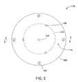
- FIG. 3is a schematic, top plan view of the heat transfer assembly of FIG. 2 .
- the present inventionis a heat transfer assembly for controlling the temperature and temperature uniformity of a substrate support in a substrate processing system.
- the substrate supportis generally used to support a substrate (e.g., silicon (Si) wafer) in a process chamber of the substrate processing system, such as a plasma etching reactor, a reactive ion etching (RIE) reactor, a chemical vapor deposition (CVD) reactor, a plasma enhanced CVD (PECVD) reactor, a physical vapor deposition (PVD) reactor, an electron cyclotron resonance (ECR) reactor, a rapid thermal processing (RTP) reactor, an ion implantation system, and the like.
- a substratee.g., silicon (Si) wafer
- RIEreactive ion etching
- CVDchemical vapor deposition
- PECVDplasma enhanced CVD
- PVDphysical vapor deposition
- ECRelectron cyclotron resonance
- RTPrapid thermal processing
- FIG. 1depicts a schematic diagram of an exemplary Decoupled Plasma Source (DPS II) etch reactor 100 that may be used to practice the invention.
- the DPS II reactoris commercially available from Applied Materials, Inc. of Santa Clara, Calif.
- the particular embodiment of the reactor 100 shown hereinis provided for illustrative purposes and should not be used to limit the scope of the invention.
- the inventioncan be used in apparatus other than a system for processing substrates, whether fabricated of semiconductor materials or other materials.
- the reactor 100comprises a process chamber 110 and a controller 140 .
- the process chamber 110generally comprises a conductive body (wall) 130 having a substantially flat dielectric ceiling 120 and encompassing a substrate support 116 .
- the process chamber 110may have other types of ceilings, e.g., a dome-shaped ceiling.
- the wall 130typically is coupled to an electrical ground terminal 134 .
- an antennacomprising at least one inductive coil element 112 (two co-axial elements 112 are shown).
- the inductive coil element 112is coupled, through a first matching network 119 , to a plasma power source 118 .
- the plasma power source 118generally is capable of producing up to 5000 W at a tunable frequency in a range from about 50 kHz to 13.6 MHz.
- the matching network 119 and the plasma power source 118are controlled by the controller 140 .
- the support pedestal 116is coupled, through a second matching network 124 , to a biasing power source 122 .
- the biasing power source 122generally is a source of up to 2000 W of continuous or pulsed power at a frequency of approximately 13.6 MHz. In other embodiments, the biasing power source 122 may be a DC or pulsed DC power source.
- the biasing power source 122 and the matching network 124are controlled by the controller 140 .
- a substrate 114is placed on the support pedestal 116 and thereafter process gases are supplied from a gas panel 138 through at least one entry port 126 to form a gaseous mixture 150 in the process chamber 110 .
- Operation of the gas panel 138is controlled by the controller 140 .
- the gaseous mixture 150is ignited to a plasma 155 in the process chamber 110 by applying power from the plasma source 118 to the at least one inductive coil element 112 , while the substrate 114 may be also biased by applying power from the biasing source 122 to the substrate support 116 .
- the lift mechanism 162is used to raise the substrate 114 off the substrate support 116 or to lower the substrate onto the substrate support.
- the lift mechanism 162comprises an actuator that engages a lift plate (both are not shown) coupled to a plurality of lift pins 172 (one lift pin is illustratively shown in FIG. 1 ).
- the lift pins 172travel through respective guide holes 188 .
- the guide holes 188are defined by an inner passage of tubes 206 that are supported by bushings 208 (discussed in reference to FIG. 2 ).
- the guide holes 188are equidistantly distributed along a circle 310 (shown in phantom in FIG. 3 ) that is concentric with the substrate support 116 .
- Such lift mechanismis disclosed in commonly assigned U.S. patent application Ser. No. 10/241,005, filed Sep. 10, 2002 (7262), which is incorporated herein by reference.
- Gas pressure within the interior of the chamber 110is controlled by the controller 140 using a throttle valve 127 and a vacuum pump 136 .
- the temperature of the wall 130may further be controlled using liquid-containing conduits (not shown) running through the wall.
- the process chamber 110also comprises conventional systems for process control, including, for example, internal process diagnostics, and the like. Such systems are collectively depicted in FIG. 1 as support systems 107 .
- the controller 140may be one of any form of general-purpose computer processor that can be used in an industrial setting for controlling various chambers and sub-processors.
- the controller 140generally comprises a central processing unit (CPU) 144 , a memory 142 , and support circuits 146 for the CPU 144 .
- ECRelectron cyclotron resonance
- CVDchemical vapor deposition
- PECVDplasma enhanced CVD
- PVDphysical vapor deposition
- RTPrapid thermal processing
- the support pedestal 116comprises a substrate support plate 160 , a heat source (such as an embedded heater) 132 , a heat transfer assembly 164 , a heat sink (such as a cooling plate) 166 , at least one bias member 190 , and a mounting assembly 106 .
- the substrate support plate 160may comprise an electrostatic chuck (as shown) or another substrate retention mechanism, e.g., a mechanical chuck, a susceptor clamp ring, vacuum chuck, and the like.
- the substrate 114In operation, the substrate 114 generally should be heated to a pre-selected temperature (e.g., from about 0 to 500 degrees Celsius). The substrate 114 is heated with minimal non-uniformity across the substrate and then maintained at such temperature.
- the temperature of the substrate 114is controlled by stabilizing the temperature of the support pedestal 116 using an embedded heater 132 and a heat transfer gas (e.g., helium (He)).
- the embedded heater 132is used to heat the support pedestal 116 while the heat transfer gas cools down the substrate 114 .
- heliumis provided to the underside of the substrate 114 from a source 148 through a gas conduit 149 to channels and grooves (not shown) formed in a top surface 174 of the substrate support plate 160 .
- an electrostatic chuckcomprises at least one clamping electrode 180 that may be conventionally controlled by a chuck power supply 176 .
- the embedded heater 132e.g., resistive electric heater
- the embedded heater 132comprises at least one heating element 182 and is regulated by a heater power supply 178 .
- the embedded heater 132is a detachable heater that is thermally coupled to a bottom surface 133 of the substrate support plate 160 .
- the at least one bias member 190applies force to the heater 132 to press it against the bottom surface 133 of the substrate support plate 160 .
- the heater 132may be embedded in the substrate support plate (e.g., electrostatic chuck) 160 or be bonded to the bottom surface 133 of the substrate support plate 160 .
- the substrate support plate 160 and embedded heater 132are generally formed from dielectric materials having a high thermal conductivity (e.g., aluminum nitride (AlN) and the like), as well as low coefficients of thermal expansion.
- the coefficients of thermal expansion for each of the substrate support plate 160 and the heater 132should be matched.
- the high thermal conductivityincreases thermal coupling between the substrate support plate 160 and the heater 132 to facilitate uniform temperatures for the support surface 174 of the plate 160 and a substrate 114 thereon.
- the matching low coefficients of thermal expansionreduce the expansion/contraction of the substrate support plate 160 relative to the heater 132 across a broad range of temperatures (e.g., from about 0 to 500 degrees Celsius).
- the heat transfer assembly 164facilitates a controlled heat sink path to the cooling plate 166 , for heat generated by the embedded heater 132 , as well as for heat produced during substrate processing, e.g., plasma processing. By regulating the total and local thermal conductivity of the heat transfer assembly 164 , temperature uniformity for the substrate support 116 may be achieved.
- the heat transfer assembly 164is used to selectively optimize over a broad range of temperatures and process parameters the thermal properties (i.e., temperature uniformity and maximum temperature) of the substrate support 116 .
- the heat transfer assembly 164comprises an electrostatic chuck and embedded heater.
- the electrostatic chuck and embedded heatermay each be of a variety of design configurations.
- the heat transfer assembly 164may be used to selectively optimize the thermal properties of a substrate support 116 having a detachable embedded heater, e.g., resistive electric heater.
- the cooling plate 166is thermally coupled to the heat transfer assembly 164 and generally, is formed from a metal, such as aluminum (Al), copper (Cu), stainless steel, and the like.
- the cooling plate 166comprises a plurality of recesses 192 , e.g., blind holes, grooves, and the like.
- Each recess 192houses a bias member 190 , including at least one cylindrical spring and the like.
- the bias member 190exerts an expanding elastic force. Such force engages the substrate support plate 160 , embedded heater 132 , heat transfer assembly 164 , and cooling plate 166 against one another and facilitates thermal coupling between the components of the substrate support 116 .
- the bias members 190are disposed such that the substrate support plate 160 , embedded heater 132 , heat transfer assembly 164 , and cooling plate 166 are uniformly compressed against one another to provide thermal coupling between the components.
- the bias members 190are disposed along at least one circle that is concentric with the substrate support 116 , e.g., around the lift pins 172 .
- the bias members 190may be similarly disposed in recesses that are formed in a surface 169 of the base plate 168 , or both in the cooling plate 166 and base plate 168 .
- the mounting assembly 106generally comprises a base plate (or ring) 168 , a collar ring 184 , a flange 194 , and a plurality of fasteners (e.g., screws, bolts, clamps, and the like) 167 .
- the fasteners 167couple the flange 194 , cooling plate 166 and base plate 168 together to provide mechanical integrity for the substrate support 116 .
- the support pedestal 116may also include various process-specific improvements, e.g., a purge gas ring, lift bellows, substrate shields, and the like.
- the collar ring 184is formed from KOVAR (i.e., an alloy comprising, by weight, about 54% iron (Fe), 29% nickel (Ni), and 17% cobalt (Co)). Further, the collar ring 184 is brazed to the substrate support plate 160 and flange 162 to facilitate gas-tight coupling between the support plate and flange.
- KOVARhas a low coefficient of thermal expansion and a low thermal conductivity and is known in the art for forming strong brazed bonds with materials, such as ceramics (support plate 160 ) and metals (flange 194 ). KOVAR is commercially available from EFI of Los Alamitos, Calif., and other suppliers.
- the mounting assembly 106encompasses an interior region 186 of the substrate support 116 .
- the interior region 186generally is maintained at a gas pressure that is higher than the gas pressure in a reaction volume 141 .
- Such higher gas pressuree.g., atmospheric pressure
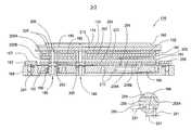
- FIG. 2 and FIG. 3are, respectively, schematic, cross-sectional and top plan views of a heat transfer assembly 164 of a substrate support 116 of the reactor 100 .
- the cross-sectional view in FIG. 2is taken along a centerline 3 - 3 in FIG. 3 .
- the heat transfer assembly 164comprises a heat spreader plate 254 that is sandwiched between a first contact plate 256 and a second contact plate 258 .
- the heat transfer assembly 164may comprise a single composite sandwich-like member.
- the embedded heater 132may be included in the heat transfer assembly 164 .
- the first and second contact plates 256 , 258are used to reduce, in a controlled manner, heat flux from the embedded heater 132 through the heat transfer assembly 164 to the cooling plate 166 .
- the cooling plate 166comprises conduits 210 that facilitate coolant flow to remove heat from the cooling plate 166 .
- the contact plates 256 , 258may be formed from materials having a low thermal conductivity, e.g., KOVAR, titanium (Ti), and the like. Generally, the contact plates 256 , 258 have a thickness of about 3 to 12 mm.
- the first contact plate 256has a flat (i.e., smooth) first contact surface 256 A and an embossed second contact surface 256 B.
- the second contact plate 258has a smooth first contact surface 258 A and an embossed second contact surface 258 B.
- the smooth first contact surfaces 256 A, 258 Aengage a bottom surface 202 of the embedded heater 132 and a bottom surface 204 of the heat spreader plate 254 , respectively.
- the embossed second contact surface 256 Bengages a top surface 203 of the heat spreader plate 254
- the embossed second contact surface 256 Bengages a top surface 205 of the cooling plate 166 .
- a surface area of the embossed second contact surfaces 256 B, 258 Bgenerally comprises about 5 to 50% of the surface area of the smooth first contact surfaces 256 A, 258 A, respectively.
- the second contact surfaces 256 B, 258 Bmay be embossed using conventional machining techniques, such as milling, turning, and the like.
- contact plates with a smaller embossed surface areaprovide a corresponding lower thermal conductivity in the direction that is orthogonal to the smooth contact surfaces. This means that contact plates 256 , 258 having a smaller embossed surface area will reduce the heat flux from the embedded heater 132 at a slower rate then contact plates having a larger embossed surface area.
- the surface area of the embossed contact surfaces 256 B, 258 Bcomprise about 20% of the surface area of the respective first contact surfaces 256 A, 258 A.
- a local pattern density for the embossed surfaces 256 B, 258 Bmay be selected such that a contact plate has a pre-determined local thermal conductivity.
- the pre-determined local thermal conductivity in one region of a contact platemay be higher or lower than the thermal conductivity in other regions of the plate.
- Such contact platesmay be used to control the flux of heat in specific regions of the heat transfer assembly 164 to improve temperature uniformity across the substrate support plate 160 as well as the substrate 114 .
- the heat spreader plate 254reduces temperature non-uniformity caused by features formed in the substrate support 116 (e.g., guide holes 188 , gas conduit 149 , the embossed surfaces 256 B, 258 B of the contact plates 256 , 258 , and the like).
- the heat spreader plate 254is formed to a thickness of about 3 to 12 mm of a material having a high thermal conductivity (e.g., aluminum nitride (AlN), copper (Cu), and the like).
- the thermal conductivity of the heat transfer assembly 164may be selectively controlled by choosing the materials and thickness for the heat spreader plate 254 and contact plates 256 , 258 , as well as a pattern and pattern density of the embossed contact surfaces 256 B, 258 B.
- the embossed contact surfaces 256 B, 258 Bcomprise a plurality of grooves 231 that are concentric with the substrate support 116 .
- Each groovehas a width 257 and depth 259 of about 4 and 3 mm, respectively, and the grooves are separated from one another by a wall having a thickness 261 of about 3 mm.
- the embossed contact surfaces 256 B, 258 Beach may comprise a plurality of parallel grooves, orthogonal grooves, grooves separated by walls having different thicknesses, and the like.
- the embossmentsgenerally have a higher pattern density in areas that oppose hotter zones of the substrate support plate 160 , the embedded heater 132 , or the substrate 114 .
- Thermally conductive sheets 213may be placed between one or more surfaces of the components comprising the substrate support 116 .
- the thermally conductive sheets 213are placed between the bottom surface 133 of the substrate support plate 160 and the embedded heater 132 (shown in FIG. 2 ), the bottom surface 202 of the embedded heater 132 and the top surface 256 A of the first contact plate 256 (not shown), the embossed surface 256 B of the first contact plate 256 and the top surface 203 of the heat spreader plate 254 (not shown), the bottom surface 204 of the heat spreader plate 254 and the top surface 258 A of the second contact plate 258 (not shown), and the embossed surface 258 B of the second contact plate and the top surface 205 of the cooling plate 166 (not shown).
- Each thermally conductive sheet 213has cutouts that conform to the surfaces of the components they separate to allow passage of lift pins 172 as well as the gas conduit 149 .
- the thermally conductive sheets 213facilitate uniform heat transfer between the components comprising the substrate support 116 , when such components are compressed by bias members 190 .
- the thermally conductive sheets 213may comprise graphite (GRAFOIL® flexible graphite commercially available from UCAR International, Inc., Arlington, Tenn.), aluminum, and the like.
- the thickness of the thermally conductive sheets 213should be within a range of about 1-5 micrometers.
- the heat transfer assembly 164 described hereinmay also be used to improve the temperature uniformity of a substrate placed on a substrate support plate (e.g., electrostatic chuck) having a detachable heater or, alternatively, a substrate support plate having an embedded heater.
- a substrate support platee.g., electrostatic chuck
- each such sealcomprises an elastic member (e.g., O-rings and the like) that is disposed in a conventional manner in a circular groove.
Landscapes
- Chemical & Material Sciences (AREA)
- General Chemical & Material Sciences (AREA)
- Chemical Kinetics & Catalysis (AREA)
- Engineering & Computer Science (AREA)
- Materials Engineering (AREA)
- Mechanical Engineering (AREA)
- Metallurgy (AREA)
- Organic Chemistry (AREA)
- Container, Conveyance, Adherence, Positioning, Of Wafer (AREA)
- Chemical Vapour Deposition (AREA)
- Drying Of Semiconductors (AREA)
Abstract
Description
1. Field of the Invention
The present invention generally relates to semiconductor substrate processing systems. More specifically, the invention relates to an apparatus for supporting a substrate in a semiconductor substrate processing system.
2. Description of the Related Art
Accurate reproducibility of substrate processing is an important factor when increasing productivity for integrated circuit fabrication processes. Precise control of various process parameters is required for achieving consistent results across a substrate, as well as results that are reproducible from substrate to substrate. More particularly, uniformity of the substrate temperature during processing is one requirement for achieving accurate reproducibility. During substrate processing, changes in the temperature and temperature gradients across the substrate are detrimental to material deposition, etch rate, step coverage, feature taper angles, and the like.
Generally, during processing, the substrate is disposed on a substrate support (e.g., electrostatic chuck, susceptor, and the like) that is thermally coupled to a heat source, such as an embedded heater, e.g., a resistive heater and the like. Additionally, in some applications, heat is also produced by the process itself (e.g., plasma process). To enhance the processing and minimize undesirable yield losses, it is essential to control the temperature as well as the temperature uniformity of the substrate.
Therefore, there is a need in the art for a substrate support having means to control the temperature as well as the temperature uniformity of the substrate.
The disadvantages associated with the prior art are overcome by an improved substrate support for a semiconductor substrate processing system. The substrate support comprises a heat transfer assembly having a heat spreader member that is sandwiched between a heat source and a heat sink. The heat sink, heat spreader member, and heat source are pressed against the bottom of a substrate support plate by a bias member.
The teachings of the present invention can be readily understood by considering the following detailed description in conjunction with the accompanying drawings, in which:
To facilitate understanding, identical reference numerals have been used, where possible, to designate identical elements that are common to the figures.
It is to be noted, however, that the appended drawings illustrate only exemplary embodiments of this invention and are therefore not to be considered limiting of its scope, for the invention may admit to other equally effective embodiments.
The present invention is a heat transfer assembly for controlling the temperature and temperature uniformity of a substrate support in a substrate processing system. The substrate support is generally used to support a substrate (e.g., silicon (Si) wafer) in a process chamber of the substrate processing system, such as a plasma etching reactor, a reactive ion etching (RIE) reactor, a chemical vapor deposition (CVD) reactor, a plasma enhanced CVD (PECVD) reactor, a physical vapor deposition (PVD) reactor, an electron cyclotron resonance (ECR) reactor, a rapid thermal processing (RTP) reactor, an ion implantation system, and the like. The invention is useful in applications that require a substrate to be supported in a chamber while the temperature of the substrate is required to be substantially uniform.
Thereactor 100 comprises aprocess chamber 110 and a controller140.
Theprocess chamber 110 generally comprises a conductive body (wall)130 having a substantially flatdielectric ceiling 120 and encompassing asubstrate support 116. Theprocess chamber 110 may have other types of ceilings, e.g., a dome-shaped ceiling. Thewall 130 typically is coupled to anelectrical ground terminal 134.
Above theceiling 120 is disposed an antenna comprising at least one inductive coil element112 (twoco-axial elements 112 are shown). Theinductive coil element 112 is coupled, through a firstmatching network 119, to aplasma power source 118. Theplasma power source 118 generally is capable of producing up to 5000 W at a tunable frequency in a range from about 50 kHz to 13.6 MHz. Thematching network 119 and theplasma power source 118 are controlled by the controller140.
Thesupport pedestal 116 is coupled, through a second matchingnetwork 124, to abiasing power source 122. Thebiasing power source 122 generally is a source of up to 2000 W of continuous or pulsed power at a frequency of approximately 13.6 MHz. In other embodiments, thebiasing power source 122 may be a DC or pulsed DC power source. Thebiasing power source 122 and thematching network 124 are controlled by the controller140.
During processing, asubstrate 114 is placed on thesupport pedestal 116 and thereafter process gases are supplied from agas panel 138 through at least oneentry port 126 to form agaseous mixture 150 in theprocess chamber 110. Operation of thegas panel 138 is controlled by the controller140. Thegaseous mixture 150 is ignited to aplasma 155 in theprocess chamber 110 by applying power from theplasma source 118 to the at least oneinductive coil element 112, while thesubstrate 114 may be also biased by applying power from thebiasing source 122 to thesubstrate support 116.
Thelift mechanism 162, as controlled by the controller140, is used to raise thesubstrate 114 off thesubstrate support 116 or to lower the substrate onto the substrate support. Generally, thelift mechanism 162 comprises an actuator that engages a lift plate (both are not shown) coupled to a plurality of lift pins172 (one lift pin is illustratively shown inFIG. 1 ). Thelift pins 172 travel throughrespective guide holes 188. Illustratively, theguide holes 188 are defined by an inner passage oftubes 206 that are supported by bushings208 (discussed in reference toFIG. 2 ).
In one embodiment, theguide holes 188 are equidistantly distributed along a circle310 (shown in phantom inFIG. 3 ) that is concentric with thesubstrate support 116. Such lift mechanism is disclosed in commonly assigned U.S. patent application Ser. No. 10/241,005, filed Sep. 10, 2002 (7262), which is incorporated herein by reference.
Gas pressure within the interior of thechamber 110 is controlled by the controller140 using athrottle valve 127 and avacuum pump 136. The temperature of thewall 130 may further be controlled using liquid-containing conduits (not shown) running through the wall. Theprocess chamber 110 also comprises conventional systems for process control, including, for example, internal process diagnostics, and the like. Such systems are collectively depicted inFIG. 1 assupport systems 107.
To facilitate control of the components and substrate processing within thechamber 110, the controller140 may be one of any form of general-purpose computer processor that can be used in an industrial setting for controlling various chambers and sub-processors. The controller140 generally comprises a central processing unit (CPU)144, amemory 142, andsupport circuits 146 for theCPU 144.
Those skilled in the art will understand that other forms of process chambers may be used to practice the invention, such as electron cyclotron resonance (ECR) chambers, chemical vapor deposition (CVD) chambers, plasma enhanced CVD (PECVD) chambers, physical vapor deposition (PVD) chambers, rapid thermal processing (RTP) chambers, and any other chamber that may incorporate a substrate support having an embedded heater therein.
In one depicted embodiment, thesupport pedestal 116 comprises asubstrate support plate 160, a heat source (such as an embedded heater)132, aheat transfer assembly 164, a heat sink (such as a cooling plate)166, at least onebias member 190, and amounting assembly 106. In alternative embodiments, thesubstrate support plate 160 may comprise an electrostatic chuck (as shown) or another substrate retention mechanism, e.g., a mechanical chuck, a susceptor clamp ring, vacuum chuck, and the like.
In operation, thesubstrate 114 generally should be heated to a pre-selected temperature (e.g., from about 0 to 500 degrees Celsius). Thesubstrate 114 is heated with minimal non-uniformity across the substrate and then maintained at such temperature. The temperature of thesubstrate 114 is controlled by stabilizing the temperature of thesupport pedestal 116 using an embeddedheater 132 and a heat transfer gas (e.g., helium (He)). The embeddedheater 132 is used to heat thesupport pedestal 116 while the heat transfer gas cools down thesubstrate 114. Generally, helium is provided to the underside of thesubstrate 114 from asource 148 through agas conduit 149 to channels and grooves (not shown) formed in atop surface 174 of thesubstrate support plate 160.
In one embodiment of thesubstrate support plate 160, an electrostatic chuck comprises at least oneclamping electrode 180 that may be conventionally controlled by achuck power supply 176. The embedded heater132 (e.g., resistive electric heater) comprises at least oneheating element 182 and is regulated by aheater power supply 178.
In one embodiment, the embeddedheater 132 is a detachable heater that is thermally coupled to abottom surface 133 of thesubstrate support plate 160. The at least onebias member 190 applies force to theheater 132 to press it against thebottom surface 133 of thesubstrate support plate 160. In an alternative embodiment, theheater 132 may be embedded in the substrate support plate (e.g., electrostatic chuck)160 or be bonded to thebottom surface 133 of thesubstrate support plate 160.
Thesubstrate support plate 160 and embeddedheater 132 are generally formed from dielectric materials having a high thermal conductivity (e.g., aluminum nitride (AlN) and the like), as well as low coefficients of thermal expansion. The coefficients of thermal expansion for each of thesubstrate support plate 160 and theheater 132 should be matched. The high thermal conductivity increases thermal coupling between thesubstrate support plate 160 and theheater 132 to facilitate uniform temperatures for thesupport surface 174 of theplate 160 and asubstrate 114 thereon. The matching low coefficients of thermal expansion reduce the expansion/contraction of thesubstrate support plate 160 relative to theheater 132 across a broad range of temperatures (e.g., from about 0 to 500 degrees Celsius).
Theheat transfer assembly 164 facilitates a controlled heat sink path to thecooling plate 166, for heat generated by the embeddedheater 132, as well as for heat produced during substrate processing, e.g., plasma processing. By regulating the total and local thermal conductivity of theheat transfer assembly 164, temperature uniformity for thesubstrate support 116 may be achieved.
Theheat transfer assembly 164 is used to selectively optimize over a broad range of temperatures and process parameters the thermal properties (i.e., temperature uniformity and maximum temperature) of thesubstrate support 116. In one embodiment, theheat transfer assembly 164 comprises an electrostatic chuck and embedded heater. The electrostatic chuck and embedded heater may each be of a variety of design configurations. Specifically, theheat transfer assembly 164 may be used to selectively optimize the thermal properties of asubstrate support 116 having a detachable embedded heater, e.g., resistive electric heater.
Thecooling plate 166 is thermally coupled to theheat transfer assembly 164 and generally, is formed from a metal, such as aluminum (Al), copper (Cu), stainless steel, and the like.
In the depicted embodiment, thecooling plate 166 comprises a plurality ofrecesses 192, e.g., blind holes, grooves, and the like. Eachrecess 192 houses abias member 190, including at least one cylindrical spring and the like. Thebias member 190 exerts an expanding elastic force. Such force engages thesubstrate support plate 160, embeddedheater 132,heat transfer assembly 164, andcooling plate 166 against one another and facilitates thermal coupling between the components of thesubstrate support 116.
Thebias members 190 are disposed such that thesubstrate support plate 160, embeddedheater 132,heat transfer assembly 164, andcooling plate 166 are uniformly compressed against one another to provide thermal coupling between the components. In one exemplary embodiment, thebias members 190 are disposed along at least one circle that is concentric with thesubstrate support 116, e.g., around the lift pins172. Alternatively, thebias members 190 may be similarly disposed in recesses that are formed in asurface 169 of thebase plate 168, or both in thecooling plate 166 andbase plate 168.
The mountingassembly 106 generally comprises a base plate (or ring)168, acollar ring 184, aflange 194, and a plurality of fasteners (e.g., screws, bolts, clamps, and the like)167. Thefasteners 167 couple theflange 194, coolingplate 166 andbase plate 168 together to provide mechanical integrity for thesubstrate support 116. In further embodiments (not shown), thesupport pedestal 116 may also include various process-specific improvements, e.g., a purge gas ring, lift bellows, substrate shields, and the like.
In one embodiment, thecollar ring 184 is formed from KOVAR (i.e., an alloy comprising, by weight, about 54% iron (Fe), 29% nickel (Ni), and 17% cobalt (Co)). Further, thecollar ring 184 is brazed to thesubstrate support plate 160 andflange 162 to facilitate gas-tight coupling between the support plate and flange. KOVAR has a low coefficient of thermal expansion and a low thermal conductivity and is known in the art for forming strong brazed bonds with materials, such as ceramics (support plate160) and metals (flange194). KOVAR is commercially available from EFI of Los Alamitos, Calif., and other suppliers.
The mountingassembly 106 encompasses aninterior region 186 of thesubstrate support 116. In operation, theinterior region 186 generally is maintained at a gas pressure that is higher than the gas pressure in areaction volume 141. Such higher gas pressure (e.g., atmospheric pressure) prevents radio-frequency arcing within thesupport pedestal 116 that otherwise is promoted by the biasingpower source 122.
Referring toFIGS. 2 and 3 , in one illustrative embodiment, theheat transfer assembly 164 comprises aheat spreader plate 254 that is sandwiched between afirst contact plate 256 and asecond contact plate 258. Alternatively, theheat transfer assembly 164 may comprise a single composite sandwich-like member. Additionally, the embeddedheater 132 may be included in theheat transfer assembly 164.
The first andsecond contact plates heater 132 through theheat transfer assembly 164 to thecooling plate 166. Thecooling plate 166 comprisesconduits 210 that facilitate coolant flow to remove heat from thecooling plate 166. Thecontact plates contact plates
Thefirst contact plate 256 has a flat (i.e., smooth)first contact surface 256A and an embossedsecond contact surface 256B. Similarly, thesecond contact plate 258 has a smoothfirst contact surface 258A and an embossedsecond contact surface 258B. The smooth first contact surfaces256A,258A engage abottom surface 202 of the embeddedheater 132 and abottom surface 204 of theheat spreader plate 254, respectively. Accordingly, the embossedsecond contact surface 256B engages atop surface 203 of theheat spreader plate 254, while the embossedsecond contact surface 256B engages atop surface 205 of thecooling plate 166.
A surface area of the embossed second contact surfaces256B,258B generally comprises about 5 to 50% of the surface area of the smooth first contact surfaces256A,258A, respectively. The second contact surfaces256B,258B may be embossed using conventional machining techniques, such as milling, turning, and the like.
Contact plates with a smaller embossed surface area provide a corresponding lower thermal conductivity in the direction that is orthogonal to the smooth contact surfaces. This means thatcontact plates heater 132 at a slower rate then contact plates having a larger embossed surface area. In one exemplary embodiment, the surface area of the embossed contact surfaces256B,258B comprise about 20% of the surface area of the respective first contact surfaces256A,258A.
Further, a local pattern density for theembossed surfaces contact surface heat transfer assembly 164 to improve temperature uniformity across thesubstrate support plate 160 as well as thesubstrate 114.
Theheat spreader plate 254 reduces temperature non-uniformity caused by features formed in the substrate support116 (e.g., guideholes 188,gas conduit 149, theembossed surfaces contact plates heat spreader plate 254 is formed to a thickness of about 3 to 12 mm of a material having a high thermal conductivity (e.g., aluminum nitride (AlN), copper (Cu), and the like).
The thermal conductivity of theheat transfer assembly 164 may be selectively controlled by choosing the materials and thickness for theheat spreader plate 254 andcontact plates
In one illustrative embodiment shown inFIG. 2 , the embossed contact surfaces256B,258B comprise a plurality ofgrooves 231 that are concentric with thesubstrate support 116. Each groove has awidth 257 anddepth 259 of about 4 and 3 mm, respectively, and the grooves are separated from one another by a wall having athickness 261 of about 3 mm.
In alternative embodiments, the embossed contact surfaces256B,258B each may comprise a plurality of parallel grooves, orthogonal grooves, grooves separated by walls having different thicknesses, and the like. To reduce temperature non-uniformity across the substrate, the embossments generally have a higher pattern density in areas that oppose hotter zones of thesubstrate support plate 160, the embeddedheater 132, or thesubstrate 114.
Thermallyconductive sheets 213 may be placed between one or more surfaces of the components comprising thesubstrate support 116. In one embodiment, the thermallyconductive sheets 213 are placed between thebottom surface 133 of thesubstrate support plate 160 and the embedded heater132 (shown inFIG. 2 ), thebottom surface 202 of the embeddedheater 132 and thetop surface 256A of the first contact plate256 (not shown), theembossed surface 256B of thefirst contact plate 256 and thetop surface 203 of the heat spreader plate254 (not shown), thebottom surface 204 of theheat spreader plate 254 and thetop surface 258A of the second contact plate258 (not shown), and theembossed surface 258B of the second contact plate and thetop surface 205 of the cooling plate166 (not shown). Each thermallyconductive sheet 213 has cutouts that conform to the surfaces of the components they separate to allow passage of lift pins172 as well as thegas conduit 149. The thermallyconductive sheets 213 facilitate uniform heat transfer between the components comprising thesubstrate support 116, when such components are compressed bybias members 190.
The thermallyconductive sheets 213 may comprise graphite (GRAFOIL® flexible graphite commercially available from UCAR International, Inc., Nashville, Tenn.), aluminum, and the like. The thickness of the thermallyconductive sheets 213 should be within a range of about 1-5 micrometers.
Theheat transfer assembly 164 described herein may also be used to improve the temperature uniformity of a substrate placed on a substrate support plate (e.g., electrostatic chuck) having a detachable heater or, alternatively, a substrate support plate having an embedded heater.
To facilitate isolation of theinterior region 186, thebase plate 168 is supplied with gas-tight seals collar ring 184 isolate theinterior region 186 from the reaction volume141 (seal281), guide hole188 (seal283), and gas conduit149 (seal285). In the illustrative embodiment shown inFIG. 2 , each such seal comprises an elastic member (e.g., O-rings and the like) that is disposed in a conventional manner in a circular groove.
Those skilled in the art will readily realize other permissible modifications of thesubstrate support 116 andheat transfer assembly 164 that facilitate advantageous in-situ control of the substrate temperature and temperature non-uniformity.
While foregoing is directed to the illustrative embodiment of the present invention, other and further embodiments of the invention may be devised without departing from the basic scope thereof, and the scope thereof is determined by the claims that follow.
Claims (30)
1. A heat transfer assembly of a substrate support for a substrate processing system, comprising:
a heat spreading member that is sandwiched between a lower surface of a first contact plate and an upper surface of a second contact plate, the first contact plate having a lower surface that is thermally coupled to an upper surface of the heat spreading member, the second contact plate having an upper surface that is thermally coupled to a lower surface of the heat spreading member along a predominant portion of the lower surface of the heat spreading member, the heat spreading member having a greater thermal conductivity than the first and second contact plates, wherein the first contact plate is thermally coupled to a heat source disposed above the lower surface of the first contact plate, the second contact plate is thermally coupled to a heat sink along a predominant portion of a bottom surface of the second contact plate, and wherein the first and second contact plates reduce heat flux between adjacent components.
2. The heat transfer assembly ofclaim 1 wherein the heat source is an embedded heater.
3. The heat transfer assembly ofclaim 2 wherein the embedded heater is a detachable heater that is thermally coupled to a substrate support plate of the substrate support.
4. The heat transfer assembly ofclaim 1 wherein the first and second contact plates each comprise one smooth contact surface and one embossed contact surface.
5. The heat transfer assembly ofclaim 4 wherein the embossed contact surface comprises an area that is about 5to 50% of the surface area of the smooth contact surface.
6. The heat transfer assembly ofclaim 4 wherein embossment in a first region of the embossed contact surface differs from embossment in at least one other region of the embossed contact surface.
7. The heat transfer assembly ofclaim 1 wherein the heat spreading member is formed of a material selected from the group consisting of aluminum nitride (AlN) and copper (Cu).
8. The heat transfer assembly ofclaim 1 wherein the first and second contact plates are formed of a material selected from the group consisting of titanium (Ti) and an alloy comprising iron (Fe), nickel (Ni) and cobalt (Co).
9. The heat transfer assembly ofclaim 1 wherein one or more thermally conductive sheets thermally couple at least two or more members selected from the group consisting of the heat spreading member, the first contact plate, the second contact plate, the heat source, the heat sink and a substrate support plate.
10. The heat transfer assembly ofclaim 9 wherein the one or more thermally conductive sheets are formed of a material selected from the group consisting of graphite and aluminum.
11. The apparatus ofclaim 1 , wherein the second contact plate is between about 3 and 12 mm thick.
12. The apparatus ofclaim 1 , wherein the heat spreading member is between about 3 and 12 mm thick.
13. Apparatus for processing a semiconductor substrate, comprising:
a process chamber; and
a substrate support disposed in the process chamber comprising a heat spreading member that is sandwiched between a lower surface of a first contact plate and an upper surface of a second contact plate, the first contact plate having a lower surface that is thermally coupled to an upper surface of the heat spreading member, the second contact plate having an upper surface that is thermally coupled to a lower surface of the heat spreading member along a predominant portion of the lower surface of the heat spreading member, the heat spreading member having a greater thermal conductivity than the first and second contact plates, wherein the first contact plate is thermally coupled to a heat source disposed above the lower surface of the first contact plate, the second contact plate is thermally coupled to a heat sink along a predominant portion of a bottom surface of the second contact plate, and wherein the first and second contact plates reduce heat flux between adjacent components.
14. The apparatus ofclaim 13 wherein the heat source is an embedded heater.
15. The apparatus ofclaim 14 wherein the embedded heater is a detachable heater that is thermally coupled to a substrate support plate of the substrate support.
16. The apparatus ofclaim 13 wherein the first and second contact plates each comprise one smooth contact surface and one embossed contact surface.
17. The apparatus ofclaim 16 wherein the embossed contact surface comprises an area that is about 5 to 50% of the surface area of the smooth contact surface.
18. The apparatus ofclaim 16 wherein embossment in a first region of the embossed contact surface differs from embossment in at least one other region of the embossed contact surface.
19. The apparatus ofclaim 16 wherein the smooth contact surface of the first contact plate engages the heat source and the embossed contact surface of the first contact plate engages the heat spreading member.
20. The apparatus ofclaim 16 wherein the smooth contact surface of the second contact plate engages the heat spreading member and the embossed contact surface of the second contact plate engages the heat sink.
21. The apparatus ofclaim 13 wherein the heat spreading member is formed of a material selected from the group consisting of aluminum nitride (AlN) and copper (Cu).
22. The apparatus ofclaim 13 wherein the first and second contact plates are formed of a material selected from the group consisting of titanium (Ti) and an alloy comprising iron (Fe), nickel (Ni) and cobalt (Co).
23. The apparatus ofclaim 13 further comprising at least one bias member that engages and thermally couples a substrate support plate, the heat source, the heat transfer assembly and the heat sink.
24. The apparatus ofclaim 23 wherein each bias member exerts an expanding elastic force.
25. The apparatus ofclaim 23 wherein each bias member is disposed in the heat sink or a base member that is coupled to the heat sink.
26. The apparatus ofclaim 23 wherein each bias member comprises at least one cylindrical spring.
27. The apparatus ofclaim 13 wherein one or more thermally conductive sheets thermally couple at least two or more members selected from the group consisting of the heat spreading member, the first contact plate, the second contact plate, the heat source, the heat sink and a substrate support plate.
28. The apparatus ofclaim 27 wherein the one or more thermally conductive sheets are formed of a material selected from the group consisting of graphite and aluminum.
29. The apparatus ofclaim 13 , wherein the second contact plate is between about 3 and 12 mm thick.
30. The apparatus ofclaim 13 , wherein the heat spreading member is between about 3 and 12 mm thick.
Priority Applications (3)
| Application Number | Priority Date | Filing Date | Title |
|---|---|---|---|
| US10/440,365US7846254B2 (en) | 2003-05-16 | 2003-05-16 | Heat transfer assembly |
| JP2004146852AJP2005051201A (en) | 2003-05-16 | 2004-05-17 | Heat transfer assembly |
| US11/535,658US20070079761A1 (en) | 2003-05-16 | 2006-09-27 | Heat transfer assembly |
Applications Claiming Priority (1)
| Application Number | Priority Date | Filing Date | Title |
|---|---|---|---|
| US10/440,365US7846254B2 (en) | 2003-05-16 | 2003-05-16 | Heat transfer assembly |
Related Child Applications (1)
| Application Number | Title | Priority Date | Filing Date |
|---|---|---|---|
| US11/535,658ContinuationUS20070079761A1 (en) | 2003-05-16 | 2006-09-27 | Heat transfer assembly |
Publications (2)
| Publication Number | Publication Date |
|---|---|
| US20040226515A1 US20040226515A1 (en) | 2004-11-18 |
| US7846254B2true US7846254B2 (en) | 2010-12-07 |
Family
ID=33417989
Family Applications (2)
| Application Number | Title | Priority Date | Filing Date |
|---|---|---|---|
| US10/440,365Expired - Fee RelatedUS7846254B2 (en) | 2003-05-16 | 2003-05-16 | Heat transfer assembly |
| US11/535,658AbandonedUS20070079761A1 (en) | 2003-05-16 | 2006-09-27 | Heat transfer assembly |
Family Applications After (1)
| Application Number | Title | Priority Date | Filing Date |
|---|---|---|---|
| US11/535,658AbandonedUS20070079761A1 (en) | 2003-05-16 | 2006-09-27 | Heat transfer assembly |
Country Status (2)
| Country | Link |
|---|---|
| US (2) | US7846254B2 (en) |
| JP (1) | JP2005051201A (en) |
Cited By (1)
| Publication number | Priority date | Publication date | Assignee | Title |
|---|---|---|---|---|
| US20140190632A1 (en)* | 2004-06-30 | 2014-07-10 | Applied Materials, Inc. | Method and apparatus for photomask plasma etching |
Families Citing this family (305)
| Publication number | Priority date | Publication date | Assignee | Title |
|---|---|---|---|---|
| KR101112029B1 (en)* | 2004-02-13 | 2012-03-21 | 에이에스엠 아메리카, 인코포레이티드 | Substrate Support System for Reduced Autodoping and Backside Deposition |
| US7691205B2 (en)* | 2005-10-18 | 2010-04-06 | Asm Japan K.K. | Substrate-supporting device |
| US8226769B2 (en)* | 2006-04-27 | 2012-07-24 | Applied Materials, Inc. | Substrate support with electrostatic chuck having dual temperature zones |
| US7838800B2 (en)* | 2006-09-25 | 2010-11-23 | Tokyo Electron Limited | Temperature controlled substrate holder having erosion resistant insulating layer for a substrate processing system |
| KR100867191B1 (en)* | 2006-11-02 | 2008-11-06 | 주식회사 유진테크 | Substrate Processing Apparatus and Substrate Processing Method |
| DE102007027704A1 (en)* | 2007-06-15 | 2008-12-18 | Aixtron Ag | Device for coating substrates arranged on a susceptor |
| JP5660753B2 (en)* | 2007-07-13 | 2015-01-28 | アプライド マテリアルズ インコーポレイテッドApplied Materials,Incorporated | High temperature cathode for plasma etching |
| JP2009084686A (en)* | 2007-09-11 | 2009-04-23 | Tokyo Electron Ltd | Substrate-placing mechanism, apparatus for processing substrate, method for suppressing film deposition on substrate placing mechanism, and storage medium |
| KR100943427B1 (en)* | 2008-02-04 | 2010-02-19 | 주식회사 유진테크 | Substrate support unit, substrate processing apparatus, and method of manufacturing the substrate support unit |
| US10192760B2 (en) | 2010-07-29 | 2019-01-29 | Eugene Technology Co., Ltd. | Substrate supporting unit, substrate processing apparatus, and method of manufacturing substrate supporting unit |
| JP5224855B2 (en)* | 2008-03-05 | 2013-07-03 | 東京エレクトロン株式会社 | Electrode unit, substrate processing apparatus, and temperature control method for electrode unit |
| JP5324251B2 (en)* | 2008-05-16 | 2013-10-23 | キヤノンアネルバ株式会社 | Substrate holding device |
| JP5564139B2 (en)* | 2008-06-13 | 2014-07-30 | キヤノンアネルバ株式会社 | Substrate holding apparatus and plasma processing apparatus |
| JP2010021510A (en)* | 2008-06-13 | 2010-01-28 | Canon Anelva Corp | Substrate support device and plasma processing apparatus |
| US8194384B2 (en)* | 2008-07-23 | 2012-06-05 | Tokyo Electron Limited | High temperature electrostatic chuck and method of using |
| US9064911B2 (en)* | 2008-10-24 | 2015-06-23 | Applied Materials, Inc. | Heated cooling plate for E-chucks and pedestals |
| US20100107974A1 (en)* | 2008-11-06 | 2010-05-06 | Asm America, Inc. | Substrate holder with varying density |
| KR100974822B1 (en) | 2009-12-15 | 2010-08-09 | 주식회사 광성테크 | Method and apparatus for pressing nickel base thin film for forming melamine sheet |
| KR20140009907A (en)* | 2011-01-10 | 2014-01-23 | 에스씨아이브이에이엑스 가부시키가이샤 | Temperature adjusting device, and imprinting device using same |
| US20130023129A1 (en) | 2011-07-20 | 2013-01-24 | Asm America, Inc. | Pressure transmitter for a semiconductor processing environment |
| US10242890B2 (en)* | 2011-08-08 | 2019-03-26 | Applied Materials, Inc. | Substrate support with heater |
| JP5989593B2 (en)* | 2012-04-27 | 2016-09-07 | 日本碍子株式会社 | Components for semiconductor manufacturing equipment |
| US10714315B2 (en) | 2012-10-12 | 2020-07-14 | Asm Ip Holdings B.V. | Semiconductor reaction chamber showerhead |
| JP5807160B2 (en)* | 2012-12-13 | 2015-11-10 | パナソニックIpマネジメント株式会社 | Non-plasma dry etching equipment |
| US20160376700A1 (en) | 2013-02-01 | 2016-12-29 | Asm Ip Holding B.V. | System for treatment of deposition reactor |
| KR101392379B1 (en)* | 2013-03-27 | 2014-05-12 | 주식회사 유진테크 | Apparatus for processing bubstrate |
| US11015245B2 (en) | 2014-03-19 | 2021-05-25 | Asm Ip Holding B.V. | Gas-phase reactor and system having exhaust plenum and components thereof |
| US10941490B2 (en) | 2014-10-07 | 2021-03-09 | Asm Ip Holding B.V. | Multiple temperature range susceptor, assembly, reactor and system including the susceptor, and methods of using the same |
| US10008404B2 (en) | 2014-10-17 | 2018-06-26 | Applied Materials, Inc. | Electrostatic chuck assembly for high temperature processes |
| US10276355B2 (en) | 2015-03-12 | 2019-04-30 | Asm Ip Holding B.V. | Multi-zone reactor, system including the reactor, and method of using the same |
| US10008399B2 (en)* | 2015-05-19 | 2018-06-26 | Applied Materials, Inc. | Electrostatic puck assembly with metal bonded backing plate for high temperature processes |
| US10458018B2 (en) | 2015-06-26 | 2019-10-29 | Asm Ip Holding B.V. | Structures including metal carbide material, devices including the structures, and methods of forming same |
| US10211308B2 (en) | 2015-10-21 | 2019-02-19 | Asm Ip Holding B.V. | NbMC layers |
| US11139308B2 (en) | 2015-12-29 | 2021-10-05 | Asm Ip Holding B.V. | Atomic layer deposition of III-V compounds to form V-NAND devices |
| US10529554B2 (en) | 2016-02-19 | 2020-01-07 | Asm Ip Holding B.V. | Method for forming silicon nitride film selectively on sidewalls or flat surfaces of trenches |
| JP6531675B2 (en)* | 2016-02-29 | 2019-06-19 | 住友大阪セメント株式会社 | Electrostatic chuck device |
| US10249526B2 (en) | 2016-03-04 | 2019-04-02 | Applied Materials, Inc. | Substrate support assembly for high temperature processes |
| US10343920B2 (en) | 2016-03-18 | 2019-07-09 | Asm Ip Holding B.V. | Aligned carbon nanotubes |
| US10367080B2 (en) | 2016-05-02 | 2019-07-30 | Asm Ip Holding B.V. | Method of forming a germanium oxynitride film |
| US11453943B2 (en) | 2016-05-25 | 2022-09-27 | Asm Ip Holding B.V. | Method for forming carbon-containing silicon/metal oxide or nitride film by ALD using silicon precursor and hydrocarbon precursor |
| US20170352565A1 (en)* | 2016-06-07 | 2017-12-07 | Chunlei Zhang | Workpiece carrier with gas pressure in inner cavities |
| US10612137B2 (en) | 2016-07-08 | 2020-04-07 | Asm Ip Holdings B.V. | Organic reactants for atomic layer deposition |
| US9859151B1 (en) | 2016-07-08 | 2018-01-02 | Asm Ip Holding B.V. | Selective film deposition method to form air gaps |
| KR102532607B1 (en) | 2016-07-28 | 2023-05-15 | 에이에스엠 아이피 홀딩 비.브이. | Substrate processing apparatus and method of operating the same |
| US9887082B1 (en) | 2016-07-28 | 2018-02-06 | Asm Ip Holding B.V. | Method and apparatus for filling a gap |
| US9812320B1 (en) | 2016-07-28 | 2017-11-07 | Asm Ip Holding B.V. | Method and apparatus for filling a gap |
| JP6847610B2 (en)* | 2016-09-14 | 2021-03-24 | 株式会社Screenホールディングス | Heat treatment equipment |
| US11532757B2 (en) | 2016-10-27 | 2022-12-20 | Asm Ip Holding B.V. | Deposition of charge trapping layers |
| US10714350B2 (en) | 2016-11-01 | 2020-07-14 | ASM IP Holdings, B.V. | Methods for forming a transition metal niobium nitride film on a substrate by atomic layer deposition and related semiconductor device structures |
| KR102546317B1 (en) | 2016-11-15 | 2023-06-21 | 에이에스엠 아이피 홀딩 비.브이. | Gas supply unit and substrate processing apparatus including the same |
| KR102762543B1 (en) | 2016-12-14 | 2025-02-05 | 에이에스엠 아이피 홀딩 비.브이. | Substrate processing apparatus |
| US11581186B2 (en) | 2016-12-15 | 2023-02-14 | Asm Ip Holding B.V. | Sequential infiltration synthesis apparatus |
| US11447861B2 (en) | 2016-12-15 | 2022-09-20 | Asm Ip Holding B.V. | Sequential infiltration synthesis apparatus and a method of forming a patterned structure |
| KR102700194B1 (en) | 2016-12-19 | 2024-08-28 | 에이에스엠 아이피 홀딩 비.브이. | Substrate processing apparatus |
| US10269558B2 (en) | 2016-12-22 | 2019-04-23 | Asm Ip Holding B.V. | Method of forming a structure on a substrate |
| US11390950B2 (en) | 2017-01-10 | 2022-07-19 | Asm Ip Holding B.V. | Reactor system and method to reduce residue buildup during a film deposition process |
| US10468261B2 (en) | 2017-02-15 | 2019-11-05 | Asm Ip Holding B.V. | Methods for forming a metallic film on a substrate by cyclical deposition and related semiconductor device structures |
| US10529563B2 (en) | 2017-03-29 | 2020-01-07 | Asm Ip Holdings B.V. | Method for forming doped metal oxide films on a substrate by cyclical deposition and related semiconductor device structures |
| JP6882040B2 (en)* | 2017-04-03 | 2021-06-02 | 日本特殊陶業株式会社 | Holding device |
| US10770286B2 (en) | 2017-05-08 | 2020-09-08 | Asm Ip Holdings B.V. | Methods for selectively forming a silicon nitride film on a substrate and related semiconductor device structures |
| US12040200B2 (en) | 2017-06-20 | 2024-07-16 | Asm Ip Holding B.V. | Semiconductor processing apparatus and methods for calibrating a semiconductor processing apparatus |
| US11306395B2 (en) | 2017-06-28 | 2022-04-19 | Asm Ip Holding B.V. | Methods for depositing a transition metal nitride film on a substrate by atomic layer deposition and related deposition apparatus |
| KR20190009245A (en) | 2017-07-18 | 2019-01-28 | 에이에스엠 아이피 홀딩 비.브이. | Methods for forming a semiconductor device structure and related semiconductor device structures |
| US10541333B2 (en) | 2017-07-19 | 2020-01-21 | Asm Ip Holding B.V. | Method for depositing a group IV semiconductor and related semiconductor device structures |
| US11018002B2 (en) | 2017-07-19 | 2021-05-25 | Asm Ip Holding B.V. | Method for selectively depositing a Group IV semiconductor and related semiconductor device structures |
| US11374112B2 (en) | 2017-07-19 | 2022-06-28 | Asm Ip Holding B.V. | Method for depositing a group IV semiconductor and related semiconductor device structures |
| US10590535B2 (en) | 2017-07-26 | 2020-03-17 | Asm Ip Holdings B.V. | Chemical treatment, deposition and/or infiltration apparatus and method for using the same |
| TWI815813B (en)* | 2017-08-04 | 2023-09-21 | 荷蘭商Asm智慧財產控股公司 | Showerhead assembly for distributing a gas within a reaction chamber |
| US10692741B2 (en) | 2017-08-08 | 2020-06-23 | Asm Ip Holdings B.V. | Radiation shield |
| US10770336B2 (en) | 2017-08-08 | 2020-09-08 | Asm Ip Holding B.V. | Substrate lift mechanism and reactor including same |
| US11769682B2 (en) | 2017-08-09 | 2023-09-26 | Asm Ip Holding B.V. | Storage apparatus for storing cassettes for substrates and processing apparatus equipped therewith |
| US11139191B2 (en) | 2017-08-09 | 2021-10-05 | Asm Ip Holding B.V. | Storage apparatus for storing cassettes for substrates and processing apparatus equipped therewith |
| US11830730B2 (en) | 2017-08-29 | 2023-11-28 | Asm Ip Holding B.V. | Layer forming method and apparatus |
| US11056344B2 (en) | 2017-08-30 | 2021-07-06 | Asm Ip Holding B.V. | Layer forming method |
| US11295980B2 (en) | 2017-08-30 | 2022-04-05 | Asm Ip Holding B.V. | Methods for depositing a molybdenum metal film over a dielectric surface of a substrate by a cyclical deposition process and related semiconductor device structures |
| KR102491945B1 (en) | 2017-08-30 | 2023-01-26 | 에이에스엠 아이피 홀딩 비.브이. | Substrate processing apparatus |
| US10658205B2 (en) | 2017-09-28 | 2020-05-19 | Asm Ip Holdings B.V. | Chemical dispensing apparatus and methods for dispensing a chemical to a reaction chamber |
| US10403504B2 (en) | 2017-10-05 | 2019-09-03 | Asm Ip Holding B.V. | Method for selectively depositing a metallic film on a substrate |
| US10923344B2 (en) | 2017-10-30 | 2021-02-16 | Asm Ip Holding B.V. | Methods for forming a semiconductor structure and related semiconductor structures |
| US11022879B2 (en) | 2017-11-24 | 2021-06-01 | Asm Ip Holding B.V. | Method of forming an enhanced unexposed photoresist layer |
| CN111344522B (en) | 2017-11-27 | 2022-04-12 | 阿斯莫Ip控股公司 | Including clean mini-environment device |
| WO2019103613A1 (en) | 2017-11-27 | 2019-05-31 | Asm Ip Holding B.V. | A storage device for storing wafer cassettes for use with a batch furnace |
| US10872771B2 (en) | 2018-01-16 | 2020-12-22 | Asm Ip Holding B. V. | Method for depositing a material film on a substrate within a reaction chamber by a cyclical deposition process and related device structures |
| TWI799494B (en) | 2018-01-19 | 2023-04-21 | 荷蘭商Asm 智慧財產控股公司 | Deposition method |
| KR102695659B1 (en) | 2018-01-19 | 2024-08-14 | 에이에스엠 아이피 홀딩 비.브이. | Method for depositing a gap filling layer by plasma assisted deposition |
| US11081345B2 (en) | 2018-02-06 | 2021-08-03 | Asm Ip Holding B.V. | Method of post-deposition treatment for silicon oxide film |
| US10896820B2 (en) | 2018-02-14 | 2021-01-19 | Asm Ip Holding B.V. | Method for depositing a ruthenium-containing film on a substrate by a cyclical deposition process |
| WO2019158960A1 (en) | 2018-02-14 | 2019-08-22 | Asm Ip Holding B.V. | A method for depositing a ruthenium-containing film on a substrate by a cyclical deposition process |
| US10731249B2 (en) | 2018-02-15 | 2020-08-04 | Asm Ip Holding B.V. | Method of forming a transition metal containing film on a substrate by a cyclical deposition process, a method for supplying a transition metal halide compound to a reaction chamber, and related vapor deposition apparatus |
| KR102636427B1 (en) | 2018-02-20 | 2024-02-13 | 에이에스엠 아이피 홀딩 비.브이. | Substrate processing method and apparatus |
| US10975470B2 (en) | 2018-02-23 | 2021-04-13 | Asm Ip Holding B.V. | Apparatus for detecting or monitoring for a chemical precursor in a high temperature environment |
| US11473195B2 (en) | 2018-03-01 | 2022-10-18 | Asm Ip Holding B.V. | Semiconductor processing apparatus and a method for processing a substrate |
| US11629406B2 (en) | 2018-03-09 | 2023-04-18 | Asm Ip Holding B.V. | Semiconductor processing apparatus comprising one or more pyrometers for measuring a temperature of a substrate during transfer of the substrate |
| US11114283B2 (en) | 2018-03-16 | 2021-09-07 | Asm Ip Holding B.V. | Reactor, system including the reactor, and methods of manufacturing and using same |
| KR102646467B1 (en) | 2018-03-27 | 2024-03-11 | 에이에스엠 아이피 홀딩 비.브이. | Method of forming an electrode on a substrate and a semiconductor device structure including an electrode |
| US11230766B2 (en) | 2018-03-29 | 2022-01-25 | Asm Ip Holding B.V. | Substrate processing apparatus and method |
| US11088002B2 (en) | 2018-03-29 | 2021-08-10 | Asm Ip Holding B.V. | Substrate rack and a substrate processing system and method |
| KR102600229B1 (en) | 2018-04-09 | 2023-11-10 | 에이에스엠 아이피 홀딩 비.브이. | Substrate supporting device, substrate processing apparatus including the same and substrate processing method |
| US12025484B2 (en) | 2018-05-08 | 2024-07-02 | Asm Ip Holding B.V. | Thin film forming method |
| TWI811348B (en) | 2018-05-08 | 2023-08-11 | 荷蘭商Asm 智慧財產控股公司 | Methods for depositing an oxide film on a substrate by a cyclical deposition process and related device structures |
| US12272527B2 (en) | 2018-05-09 | 2025-04-08 | Asm Ip Holding B.V. | Apparatus for use with hydrogen radicals and method of using same |
| KR102596988B1 (en) | 2018-05-28 | 2023-10-31 | 에이에스엠 아이피 홀딩 비.브이. | Method of processing a substrate and a device manufactured by the same |
| TWI840362B (en) | 2018-06-04 | 2024-05-01 | 荷蘭商Asm Ip私人控股有限公司 | Wafer handling chamber with moisture reduction |
| US11718913B2 (en) | 2018-06-04 | 2023-08-08 | Asm Ip Holding B.V. | Gas distribution system and reactor system including same |
| US11286562B2 (en) | 2018-06-08 | 2022-03-29 | Asm Ip Holding B.V. | Gas-phase chemical reactor and method of using same |
| US10797133B2 (en) | 2018-06-21 | 2020-10-06 | Asm Ip Holding B.V. | Method for depositing a phosphorus doped silicon arsenide film and related semiconductor device structures |
| KR102568797B1 (en) | 2018-06-21 | 2023-08-21 | 에이에스엠 아이피 홀딩 비.브이. | Substrate processing system |
| TWI873894B (en) | 2018-06-27 | 2025-02-21 | 荷蘭商Asm Ip私人控股有限公司 | Cyclic deposition methods for forming metal-containing material and films and structures including the metal-containing material |
| KR102854019B1 (en) | 2018-06-27 | 2025-09-02 | 에이에스엠 아이피 홀딩 비.브이. | Periodic deposition method for forming a metal-containing material and films and structures comprising the metal-containing material |
| US10612136B2 (en) | 2018-06-29 | 2020-04-07 | ASM IP Holding, B.V. | Temperature-controlled flange and reactor system including same |
| US10388513B1 (en) | 2018-07-03 | 2019-08-20 | Asm Ip Holding B.V. | Method for depositing silicon-free carbon-containing film as gap-fill layer by pulse plasma-assisted deposition |
| US10755922B2 (en) | 2018-07-03 | 2020-08-25 | Asm Ip Holding B.V. | Method for depositing silicon-free carbon-containing film as gap-fill layer by pulse plasma-assisted deposition |
| US11053591B2 (en) | 2018-08-06 | 2021-07-06 | Asm Ip Holding B.V. | Multi-port gas injection system and reactor system including same |
| US11430674B2 (en) | 2018-08-22 | 2022-08-30 | Asm Ip Holding B.V. | Sensor array, apparatus for dispensing a vapor phase reactant to a reaction chamber and related methods |
| KR102707956B1 (en) | 2018-09-11 | 2024-09-19 | 에이에스엠 아이피 홀딩 비.브이. | Method for deposition of a thin film |
| US11024523B2 (en) | 2018-09-11 | 2021-06-01 | Asm Ip Holding B.V. | Substrate processing apparatus and method |
| US11049751B2 (en) | 2018-09-14 | 2021-06-29 | Asm Ip Holding B.V. | Cassette supply system to store and handle cassettes and processing apparatus equipped therewith |
| CN110970344B (en) | 2018-10-01 | 2024-10-25 | Asmip控股有限公司 | Substrate holding apparatus, system comprising the same and method of using the same |
| US11232963B2 (en) | 2018-10-03 | 2022-01-25 | Asm Ip Holding B.V. | Substrate processing apparatus and method |
| KR102592699B1 (en) | 2018-10-08 | 2023-10-23 | 에이에스엠 아이피 홀딩 비.브이. | Substrate support unit and apparatuses for depositing thin film and processing the substrate including the same |
| KR102605121B1 (en) | 2018-10-19 | 2023-11-23 | 에이에스엠 아이피 홀딩 비.브이. | Substrate processing apparatus and substrate processing method |
| KR102546322B1 (en) | 2018-10-19 | 2023-06-21 | 에이에스엠 아이피 홀딩 비.브이. | Substrate processing apparatus and substrate processing method |
| USD948463S1 (en) | 2018-10-24 | 2022-04-12 | Asm Ip Holding B.V. | Susceptor for semiconductor substrate supporting apparatus |
| US12378665B2 (en) | 2018-10-26 | 2025-08-05 | Asm Ip Holding B.V. | High temperature coatings for a preclean and etch apparatus and related methods |
| US11087997B2 (en) | 2018-10-31 | 2021-08-10 | Asm Ip Holding B.V. | Substrate processing apparatus for processing substrates |
| KR102748291B1 (en) | 2018-11-02 | 2024-12-31 | 에이에스엠 아이피 홀딩 비.브이. | Substrate support unit and substrate processing apparatus including the same |
| US11572620B2 (en) | 2018-11-06 | 2023-02-07 | Asm Ip Holding B.V. | Methods for selectively depositing an amorphous silicon film on a substrate |
| US11031242B2 (en) | 2018-11-07 | 2021-06-08 | Asm Ip Holding B.V. | Methods for depositing a boron doped silicon germanium film |
| US10818758B2 (en) | 2018-11-16 | 2020-10-27 | Asm Ip Holding B.V. | Methods for forming a metal silicate film on a substrate in a reaction chamber and related semiconductor device structures |
| US10847366B2 (en) | 2018-11-16 | 2020-11-24 | Asm Ip Holding B.V. | Methods for depositing a transition metal chalcogenide film on a substrate by a cyclical deposition process |
| US12040199B2 (en) | 2018-11-28 | 2024-07-16 | Asm Ip Holding B.V. | Substrate processing apparatus for processing substrates |
| US11217444B2 (en) | 2018-11-30 | 2022-01-04 | Asm Ip Holding B.V. | Method for forming an ultraviolet radiation responsive metal oxide-containing film |
| KR102636428B1 (en) | 2018-12-04 | 2024-02-13 | 에이에스엠 아이피 홀딩 비.브이. | A method for cleaning a substrate processing apparatus |
| US11158513B2 (en) | 2018-12-13 | 2021-10-26 | Asm Ip Holding B.V. | Methods for forming a rhenium-containing film on a substrate by a cyclical deposition process and related semiconductor device structures |
| TWI874340B (en) | 2018-12-14 | 2025-03-01 | 荷蘭商Asm Ip私人控股有限公司 | Method of forming device structure, structure formed by the method and system for performing the method |
| TWI866480B (en) | 2019-01-17 | 2024-12-11 | 荷蘭商Asm Ip 私人控股有限公司 | Methods of forming a transition metal containing film on a substrate by a cyclical deposition process |
| KR102727227B1 (en) | 2019-01-22 | 2024-11-07 | 에이에스엠 아이피 홀딩 비.브이. | Semiconductor processing device |
| CN111524788B (en) | 2019-02-01 | 2023-11-24 | Asm Ip私人控股有限公司 | Method for forming topologically selective films of silicon oxide |
| TWI873122B (en) | 2019-02-20 | 2025-02-21 | 荷蘭商Asm Ip私人控股有限公司 | Method of filling a recess formed within a surface of a substrate, semiconductor structure formed according to the method, and semiconductor processing apparatus |
| KR102626263B1 (en) | 2019-02-20 | 2024-01-16 | 에이에스엠 아이피 홀딩 비.브이. | Cyclical deposition method including treatment step and apparatus for same |
| TWI845607B (en) | 2019-02-20 | 2024-06-21 | 荷蘭商Asm Ip私人控股有限公司 | Cyclical deposition method and apparatus for filling a recess formed within a substrate surface |
| TWI838458B (en) | 2019-02-20 | 2024-04-11 | 荷蘭商Asm Ip私人控股有限公司 | Apparatus and methods for plug fill deposition in 3-d nand applications |
| TWI842826B (en) | 2019-02-22 | 2024-05-21 | 荷蘭商Asm Ip私人控股有限公司 | Substrate processing apparatus and method for processing substrate |
| US11742198B2 (en) | 2019-03-08 | 2023-08-29 | Asm Ip Holding B.V. | Structure including SiOCN layer and method of forming same |
| KR102782593B1 (en) | 2019-03-08 | 2025-03-14 | 에이에스엠 아이피 홀딩 비.브이. | Structure Including SiOC Layer and Method of Forming Same |
| KR102858005B1 (en) | 2019-03-08 | 2025-09-09 | 에이에스엠 아이피 홀딩 비.브이. | Method for Selective Deposition of Silicon Nitride Layer and Structure Including Selectively-Deposited Silicon Nitride Layer |
| JP2020167398A (en) | 2019-03-28 | 2020-10-08 | エーエスエム・アイピー・ホールディング・ベー・フェー | Door openers and substrate processing equipment provided with door openers |
| KR102809999B1 (en) | 2019-04-01 | 2025-05-19 | 에이에스엠 아이피 홀딩 비.브이. | Method of manufacturing semiconductor device |
| KR20200123380A (en) | 2019-04-19 | 2020-10-29 | 에이에스엠 아이피 홀딩 비.브이. | Layer forming method and apparatus |
| KR20200125453A (en) | 2019-04-24 | 2020-11-04 | 에이에스엠 아이피 홀딩 비.브이. | Gas-phase reactor system and method of using same |
| US11289326B2 (en) | 2019-05-07 | 2022-03-29 | Asm Ip Holding B.V. | Method for reforming amorphous carbon polymer film |
| KR20200130121A (en) | 2019-05-07 | 2020-11-18 | 에이에스엠 아이피 홀딩 비.브이. | Chemical source vessel with dip tube |
| KR20200130652A (en) | 2019-05-10 | 2020-11-19 | 에이에스엠 아이피 홀딩 비.브이. | Method of depositing material onto a surface and structure formed according to the method |
| JP7612342B2 (en) | 2019-05-16 | 2025-01-14 | エーエスエム・アイピー・ホールディング・ベー・フェー | Wafer boat handling apparatus, vertical batch furnace and method |
| JP7598201B2 (en) | 2019-05-16 | 2024-12-11 | エーエスエム・アイピー・ホールディング・ベー・フェー | Wafer boat handling apparatus, vertical batch furnace and method |
| USD947913S1 (en) | 2019-05-17 | 2022-04-05 | Asm Ip Holding B.V. | Susceptor shaft |
| USD975665S1 (en) | 2019-05-17 | 2023-01-17 | Asm Ip Holding B.V. | Susceptor shaft |
| USD935572S1 (en) | 2019-05-24 | 2021-11-09 | Asm Ip Holding B.V. | Gas channel plate |
| USD922229S1 (en) | 2019-06-05 | 2021-06-15 | Asm Ip Holding B.V. | Device for controlling a temperature of a gas supply unit |
| KR20200141002A (en) | 2019-06-06 | 2020-12-17 | 에이에스엠 아이피 홀딩 비.브이. | Method of using a gas-phase reactor system including analyzing exhausted gas |
| KR20200141931A (en) | 2019-06-10 | 2020-12-21 | 에이에스엠 아이피 홀딩 비.브이. | Method for cleaning quartz epitaxial chambers |
| KR20200143254A (en) | 2019-06-11 | 2020-12-23 | 에이에스엠 아이피 홀딩 비.브이. | Method of forming an electronic structure using an reforming gas, system for performing the method, and structure formed using the method |
| USD944946S1 (en) | 2019-06-14 | 2022-03-01 | Asm Ip Holding B.V. | Shower plate |
| USD931978S1 (en) | 2019-06-27 | 2021-09-28 | Asm Ip Holding B.V. | Showerhead vacuum transport |
| KR20210005515A (en) | 2019-07-03 | 2021-01-14 | 에이에스엠 아이피 홀딩 비.브이. | Temperature control assembly for substrate processing apparatus and method of using same |
| JP7499079B2 (en) | 2019-07-09 | 2024-06-13 | エーエスエム・アイピー・ホールディング・ベー・フェー | Plasma device using coaxial waveguide and substrate processing method |
| CN112216646A (en) | 2019-07-10 | 2021-01-12 | Asm Ip私人控股有限公司 | Substrate supporting assembly and substrate processing device comprising same |
| KR20210010307A (en) | 2019-07-16 | 2021-01-27 | 에이에스엠 아이피 홀딩 비.브이. | Substrate processing apparatus |
| KR20210010816A (en) | 2019-07-17 | 2021-01-28 | 에이에스엠 아이피 홀딩 비.브이. | Radical assist ignition plasma system and method |
| KR102860110B1 (en) | 2019-07-17 | 2025-09-16 | 에이에스엠 아이피 홀딩 비.브이. | Methods of forming silicon germanium structures |
| US11643724B2 (en) | 2019-07-18 | 2023-05-09 | Asm Ip Holding B.V. | Method of forming structures using a neutral beam |
| KR20210010817A (en) | 2019-07-19 | 2021-01-28 | 에이에스엠 아이피 홀딩 비.브이. | Method of Forming Topology-Controlled Amorphous Carbon Polymer Film |
| TWI839544B (en) | 2019-07-19 | 2024-04-21 | 荷蘭商Asm Ip私人控股有限公司 | Method of forming topology-controlled amorphous carbon polymer film |
| TWI851767B (en) | 2019-07-29 | 2024-08-11 | 荷蘭商Asm Ip私人控股有限公司 | Methods for selective deposition utilizing n-type dopants and/or alternative dopants to achieve high dopant incorporation |
| CN112309899A (en) | 2019-07-30 | 2021-02-02 | Asm Ip私人控股有限公司 | Substrate processing apparatus |
| CN112309900A (en) | 2019-07-30 | 2021-02-02 | Asm Ip私人控股有限公司 | Substrate processing apparatus |
| US12169361B2 (en) | 2019-07-30 | 2024-12-17 | Asm Ip Holding B.V. | Substrate processing apparatus and method |
| US11587814B2 (en) | 2019-07-31 | 2023-02-21 | Asm Ip Holding B.V. | Vertical batch furnace assembly |
| US11227782B2 (en) | 2019-07-31 | 2022-01-18 | Asm Ip Holding B.V. | Vertical batch furnace assembly |
| US11587815B2 (en) | 2019-07-31 | 2023-02-21 | Asm Ip Holding B.V. | Vertical batch furnace assembly |
| US20220262657A1 (en)* | 2019-08-02 | 2022-08-18 | Applied Materials, Inc. | Pedestal with multi-zone heating |
| CN112323048B (en) | 2019-08-05 | 2024-02-09 | Asm Ip私人控股有限公司 | Liquid level sensor for chemical source container |
| CN112342526A (en) | 2019-08-09 | 2021-02-09 | Asm Ip私人控股有限公司 | Heater assembly including cooling device and method of using same |
| USD965044S1 (en) | 2019-08-19 | 2022-09-27 | Asm Ip Holding B.V. | Susceptor shaft |
| USD965524S1 (en) | 2019-08-19 | 2022-10-04 | Asm Ip Holding B.V. | Susceptor support |
| JP2021031769A (en) | 2019-08-21 | 2021-03-01 | エーエスエム アイピー ホールディング ビー.ブイ. | Production apparatus of mixed gas of film deposition raw material and film deposition apparatus |
| USD949319S1 (en) | 2019-08-22 | 2022-04-19 | Asm Ip Holding B.V. | Exhaust duct |
| KR20210024423A (en) | 2019-08-22 | 2021-03-05 | 에이에스엠 아이피 홀딩 비.브이. | Method for forming a structure with a hole |
| USD940837S1 (en) | 2019-08-22 | 2022-01-11 | Asm Ip Holding B.V. | Electrode |
| USD930782S1 (en) | 2019-08-22 | 2021-09-14 | Asm Ip Holding B.V. | Gas distributor |
| USD979506S1 (en) | 2019-08-22 | 2023-02-28 | Asm Ip Holding B.V. | Insulator |
| US11286558B2 (en) | 2019-08-23 | 2022-03-29 | Asm Ip Holding B.V. | Methods for depositing a molybdenum nitride film on a surface of a substrate by a cyclical deposition process and related semiconductor device structures including a molybdenum nitride film |
| KR20210024420A (en) | 2019-08-23 | 2021-03-05 | 에이에스엠 아이피 홀딩 비.브이. | Method for depositing silicon oxide film having improved quality by peald using bis(diethylamino)silane |
| KR102806450B1 (en) | 2019-09-04 | 2025-05-12 | 에이에스엠 아이피 홀딩 비.브이. | Methods for selective deposition using a sacrificial capping layer |
| KR102733104B1 (en) | 2019-09-05 | 2024-11-22 | 에이에스엠 아이피 홀딩 비.브이. | Substrate processing apparatus |
| US11562901B2 (en) | 2019-09-25 | 2023-01-24 | Asm Ip Holding B.V. | Substrate processing method |
| CN112593212B (en) | 2019-10-02 | 2023-12-22 | Asm Ip私人控股有限公司 | Method for forming topologically selective silicon oxide film by cyclic plasma enhanced deposition process |
| TWI846953B (en) | 2019-10-08 | 2024-07-01 | 荷蘭商Asm Ip私人控股有限公司 | Substrate processing device |
| TW202128273A (en) | 2019-10-08 | 2021-08-01 | 荷蘭商Asm Ip私人控股有限公司 | Gas injection system, reactor system, and method of depositing material on surface of substratewithin reaction chamber |
| CN114556217A (en) | 2019-10-08 | 2022-05-27 | 应用材料公司 | Generic metrology documentation, protocols, and processes for maskless lithography systems |
| KR20210042810A (en) | 2019-10-08 | 2021-04-20 | 에이에스엠 아이피 홀딩 비.브이. | Reactor system including a gas distribution assembly for use with activated species and method of using same |
| TWI846966B (en) | 2019-10-10 | 2024-07-01 | 荷蘭商Asm Ip私人控股有限公司 | Method of forming a photoresist underlayer and structure including same |
| US12009241B2 (en) | 2019-10-14 | 2024-06-11 | Asm Ip Holding B.V. | Vertical batch furnace assembly with detector to detect cassette |
| TWI834919B (en) | 2019-10-16 | 2024-03-11 | 荷蘭商Asm Ip私人控股有限公司 | Method of topology-selective film formation of silicon oxide |
| US11637014B2 (en) | 2019-10-17 | 2023-04-25 | Asm Ip Holding B.V. | Methods for selective deposition of doped semiconductor material |
| KR102845724B1 (en) | 2019-10-21 | 2025-08-13 | 에이에스엠 아이피 홀딩 비.브이. | Apparatus and methods for selectively etching films |
| KR20210050453A (en) | 2019-10-25 | 2021-05-07 | 에이에스엠 아이피 홀딩 비.브이. | Methods for filling a gap feature on a substrate surface and related semiconductor structures |
| US11646205B2 (en) | 2019-10-29 | 2023-05-09 | Asm Ip Holding B.V. | Methods of selectively forming n-type doped material on a surface, systems for selectively forming n-type doped material, and structures formed using same |
| KR20210054983A (en) | 2019-11-05 | 2021-05-14 | 에이에스엠 아이피 홀딩 비.브이. | Structures with doped semiconductor layers and methods and systems for forming same |
| US11501968B2 (en) | 2019-11-15 | 2022-11-15 | Asm Ip Holding B.V. | Method for providing a semiconductor device with silicon filled gaps |
| KR102861314B1 (en) | 2019-11-20 | 2025-09-17 | 에이에스엠 아이피 홀딩 비.브이. | Method of depositing carbon-containing material on a surface of a substrate, structure formed using the method, and system for forming the structure |
| US11450529B2 (en) | 2019-11-26 | 2022-09-20 | Asm Ip Holding B.V. | Methods for selectively forming a target film on a substrate comprising a first dielectric surface and a second metallic surface |
| CN112951697B (en) | 2019-11-26 | 2025-07-29 | Asmip私人控股有限公司 | Substrate processing apparatus |
| CN112885692B (en) | 2019-11-29 | 2025-08-15 | Asmip私人控股有限公司 | Substrate processing apparatus |
| CN120432376A (en) | 2019-11-29 | 2025-08-05 | Asm Ip私人控股有限公司 | Substrate processing apparatus |
| JP7527928B2 (en) | 2019-12-02 | 2024-08-05 | エーエスエム・アイピー・ホールディング・ベー・フェー | Substrate processing apparatus and substrate processing method |
| KR20210070898A (en) | 2019-12-04 | 2021-06-15 | 에이에스엠 아이피 홀딩 비.브이. | Substrate processing apparatus |
| KR20210078405A (en) | 2019-12-17 | 2021-06-28 | 에이에스엠 아이피 홀딩 비.브이. | Method of forming vanadium nitride layer and structure including the vanadium nitride layer |
| KR20210080214A (en) | 2019-12-19 | 2021-06-30 | 에이에스엠 아이피 홀딩 비.브이. | Methods for filling a gap feature on a substrate and related semiconductor structures |
| JP7636892B2 (en) | 2020-01-06 | 2025-02-27 | エーエスエム・アイピー・ホールディング・ベー・フェー | Channeled Lift Pins |
| JP7730637B2 (en) | 2020-01-06 | 2025-08-28 | エーエスエム・アイピー・ホールディング・ベー・フェー | Gas delivery assembly, components thereof, and reactor system including same |
| US11993847B2 (en) | 2020-01-08 | 2024-05-28 | Asm Ip Holding B.V. | Injector |
| KR20210093163A (en) | 2020-01-16 | 2021-07-27 | 에이에스엠 아이피 홀딩 비.브이. | Method of forming high aspect ratio features |
| KR102675856B1 (en) | 2020-01-20 | 2024-06-17 | 에이에스엠 아이피 홀딩 비.브이. | Method of forming thin film and method of modifying surface of thin film |
| TWI889744B (en) | 2020-01-29 | 2025-07-11 | 荷蘭商Asm Ip私人控股有限公司 | Contaminant trap system, and baffle plate stack |
| TW202513845A (en) | 2020-02-03 | 2025-04-01 | 荷蘭商Asm Ip私人控股有限公司 | Semiconductor structures and methods for forming the same |
| KR20210100010A (en) | 2020-02-04 | 2021-08-13 | 에이에스엠 아이피 홀딩 비.브이. | Method and apparatus for transmittance measurements of large articles |
| US11776846B2 (en) | 2020-02-07 | 2023-10-03 | Asm Ip Holding B.V. | Methods for depositing gap filling fluids and related systems and devices |
| TW202146691A (en) | 2020-02-13 | 2021-12-16 | 荷蘭商Asm Ip私人控股有限公司 | Gas distribution assembly, shower plate assembly, and method of adjusting conductance of gas to reaction chamber |
| KR20210103956A (en) | 2020-02-13 | 2021-08-24 | 에이에스엠 아이피 홀딩 비.브이. | Substrate processing apparatus including light receiving device and calibration method of light receiving device |
| TWI855223B (en) | 2020-02-17 | 2024-09-11 | 荷蘭商Asm Ip私人控股有限公司 | Method for growing phosphorous-doped silicon layer |
| CN113410160A (en) | 2020-02-28 | 2021-09-17 | Asm Ip私人控股有限公司 | System specially used for cleaning parts |
| KR20210113043A (en) | 2020-03-04 | 2021-09-15 | 에이에스엠 아이피 홀딩 비.브이. | Alignment fixture for a reactor system |
| KR20210116240A (en) | 2020-03-11 | 2021-09-27 | 에이에스엠 아이피 홀딩 비.브이. | Substrate handling device with adjustable joints |
| US11876356B2 (en) | 2020-03-11 | 2024-01-16 | Asm Ip Holding B.V. | Lockout tagout assembly and system and method of using same |
| KR102775390B1 (en) | 2020-03-12 | 2025-02-28 | 에이에스엠 아이피 홀딩 비.브이. | Method for Fabricating Layer Structure Having Target Topological Profile |
| US12173404B2 (en) | 2020-03-17 | 2024-12-24 | Asm Ip Holding B.V. | Method of depositing epitaxial material, structure formed using the method, and system for performing the method |
| KR102755229B1 (en) | 2020-04-02 | 2025-01-14 | 에이에스엠 아이피 홀딩 비.브이. | Thin film forming method |
| TWI887376B (en) | 2020-04-03 | 2025-06-21 | 荷蘭商Asm Ip私人控股有限公司 | Method for manufacturing semiconductor device |
| TWI888525B (en) | 2020-04-08 | 2025-07-01 | 荷蘭商Asm Ip私人控股有限公司 | Apparatus and methods for selectively etching silcon oxide films |
| US11821078B2 (en) | 2020-04-15 | 2023-11-21 | Asm Ip Holding B.V. | Method for forming precoat film and method for forming silicon-containing film |
| KR20210128343A (en) | 2020-04-15 | 2021-10-26 | 에이에스엠 아이피 홀딩 비.브이. | Method of forming chromium nitride layer and structure including the chromium nitride layer |
| US11996289B2 (en) | 2020-04-16 | 2024-05-28 | Asm Ip Holding B.V. | Methods of forming structures including silicon germanium and silicon layers, devices formed using the methods, and systems for performing the methods |
| KR20210130646A (en) | 2020-04-21 | 2021-11-01 | 에이에스엠 아이피 홀딩 비.브이. | Method for processing a substrate |
| CN113555279A (en) | 2020-04-24 | 2021-10-26 | Asm Ip私人控股有限公司 | Methods of forming vanadium nitride-containing layers and structures comprising the same |
| KR20210132612A (en) | 2020-04-24 | 2021-11-04 | 에이에스엠 아이피 홀딩 비.브이. | Methods and apparatus for stabilizing vanadium compounds |
| TW202208671A (en) | 2020-04-24 | 2022-03-01 | 荷蘭商Asm Ip私人控股有限公司 | Methods of forming structures including vanadium boride and vanadium phosphide layers |
| KR20210132600A (en) | 2020-04-24 | 2021-11-04 | 에이에스엠 아이피 홀딩 비.브이. | Methods and systems for depositing a layer comprising vanadium, nitrogen, and a further element |
| KR102866804B1 (en) | 2020-04-24 | 2025-09-30 | 에이에스엠 아이피 홀딩 비.브이. | Vertical batch furnace assembly comprising a cooling gas supply |
| KR102783898B1 (en) | 2020-04-29 | 2025-03-18 | 에이에스엠 아이피 홀딩 비.브이. | Solid source precursor vessel |
| KR20210134869A (en) | 2020-05-01 | 2021-11-11 | 에이에스엠 아이피 홀딩 비.브이. | Fast FOUP swapping with a FOUP handler |
| JP7726664B2 (en) | 2020-05-04 | 2025-08-20 | エーエスエム・アイピー・ホールディング・ベー・フェー | Substrate processing system for processing a substrate |
| KR102788543B1 (en) | 2020-05-13 | 2025-03-27 | 에이에스엠 아이피 홀딩 비.브이. | Laser alignment fixture for a reactor system |
| TW202146699A (en) | 2020-05-15 | 2021-12-16 | 荷蘭商Asm Ip私人控股有限公司 | Method of forming a silicon germanium layer, semiconductor structure, semiconductor device, method of forming a deposition layer, and deposition system |
| KR20210143653A (en) | 2020-05-19 | 2021-11-29 | 에이에스엠 아이피 홀딩 비.브이. | Substrate processing apparatus |
| KR102795476B1 (en) | 2020-05-21 | 2025-04-11 | 에이에스엠 아이피 홀딩 비.브이. | Structures including multiple carbon layers and methods of forming and using same |
| KR20210145079A (en) | 2020-05-21 | 2021-12-01 | 에이에스엠 아이피 홀딩 비.브이. | Flange and apparatus for processing substrates |
| TWI873343B (en) | 2020-05-22 | 2025-02-21 | 荷蘭商Asm Ip私人控股有限公司 | Reaction system for forming thin film on substrate |
| KR20210146802A (en) | 2020-05-26 | 2021-12-06 | 에이에스엠 아이피 홀딩 비.브이. | Method for depositing boron and gallium containing silicon germanium layers |
| TWI876048B (en) | 2020-05-29 | 2025-03-11 | 荷蘭商Asm Ip私人控股有限公司 | Substrate processing device |
| TW202212620A (en) | 2020-06-02 | 2022-04-01 | 荷蘭商Asm Ip私人控股有限公司 | Apparatus for processing substrate, method of forming film, and method of controlling apparatus for processing substrate |
| TW202208659A (en) | 2020-06-16 | 2022-03-01 | 荷蘭商Asm Ip私人控股有限公司 | Method for depositing boron containing silicon germanium layers |
| TW202218133A (en) | 2020-06-24 | 2022-05-01 | 荷蘭商Asm Ip私人控股有限公司 | Method for forming a layer provided with silicon |
| TWI873359B (en) | 2020-06-30 | 2025-02-21 | 荷蘭商Asm Ip私人控股有限公司 | Substrate processing method |
| US12431354B2 (en) | 2020-07-01 | 2025-09-30 | Asm Ip Holding B.V. | Silicon nitride and silicon oxide deposition methods using fluorine inhibitor |
| TW202202649A (en) | 2020-07-08 | 2022-01-16 | 荷蘭商Asm Ip私人控股有限公司 | Substrate processing method |
| KR20220010438A (en) | 2020-07-17 | 2022-01-25 | 에이에스엠 아이피 홀딩 비.브이. | Structures and methods for use in photolithography |
| KR20220011092A (en) | 2020-07-20 | 2022-01-27 | 에이에스엠 아이피 홀딩 비.브이. | Method and system for forming structures including transition metal layers |
| TWI878570B (en) | 2020-07-20 | 2025-04-01 | 荷蘭商Asm Ip私人控股有限公司 | Method and system for depositing molybdenum layers |
| US12322591B2 (en) | 2020-07-27 | 2025-06-03 | Asm Ip Holding B.V. | Thin film deposition process |
| KR20220021863A (en) | 2020-08-14 | 2022-02-22 | 에이에스엠 아이피 홀딩 비.브이. | Method for processing a substrate |
| US12040177B2 (en) | 2020-08-18 | 2024-07-16 | Asm Ip Holding B.V. | Methods for forming a laminate film by cyclical plasma-enhanced deposition processes |
| TW202228863A (en) | 2020-08-25 | 2022-08-01 | 荷蘭商Asm Ip私人控股有限公司 | Method for cleaning a substrate, method for selectively depositing, and reaction system |
| CN111968901B (en)* | 2020-08-25 | 2022-08-16 | 北京北方华创微电子装备有限公司 | Semiconductor reaction chamber and semiconductor processing equipment |
| US11725280B2 (en) | 2020-08-26 | 2023-08-15 | Asm Ip Holding B.V. | Method for forming metal silicon oxide and metal silicon oxynitride layers |
| TW202229601A (en) | 2020-08-27 | 2022-08-01 | 荷蘭商Asm Ip私人控股有限公司 | Method of forming patterned structures, method of manipulating mechanical property, device structure, and substrate processing system |
| TW202217045A (en) | 2020-09-10 | 2022-05-01 | 荷蘭商Asm Ip私人控股有限公司 | Methods for depositing gap filing fluids and related systems and devices |
| USD990534S1 (en) | 2020-09-11 | 2023-06-27 | Asm Ip Holding B.V. | Weighted lift pin |
| KR20220036866A (en) | 2020-09-16 | 2022-03-23 | 에이에스엠 아이피 홀딩 비.브이. | Silicon oxide deposition method |
| USD1012873S1 (en) | 2020-09-24 | 2024-01-30 | Asm Ip Holding B.V. | Electrode for semiconductor processing apparatus |
| TWI889903B (en) | 2020-09-25 | 2025-07-11 | 荷蘭商Asm Ip私人控股有限公司 | Semiconductor processing method |
| US12009224B2 (en) | 2020-09-29 | 2024-06-11 | Asm Ip Holding B.V. | Apparatus and method for etching metal nitrides |
| KR20220045900A (en) | 2020-10-06 | 2022-04-13 | 에이에스엠 아이피 홀딩 비.브이. | Deposition method and an apparatus for depositing a silicon-containing material |
| CN114293174A (en) | 2020-10-07 | 2022-04-08 | Asm Ip私人控股有限公司 | Gas supply unit and substrate processing apparatus including the same |
| TW202229613A (en) | 2020-10-14 | 2022-08-01 | 荷蘭商Asm Ip私人控股有限公司 | Method of depositing material on stepped structure |
| TW202232565A (en) | 2020-10-15 | 2022-08-16 | 荷蘭商Asm Ip私人控股有限公司 | Method of manufacturing semiconductor device, and substrate treatment apparatus using ether-cat |
| TW202217037A (en) | 2020-10-22 | 2022-05-01 | 荷蘭商Asm Ip私人控股有限公司 | Method of depositing vanadium metal, structure, device and a deposition assembly |
| TW202223136A (en) | 2020-10-28 | 2022-06-16 | 荷蘭商Asm Ip私人控股有限公司 | Method for forming layer on substrate, and semiconductor processing system |
| TW202229620A (en) | 2020-11-12 | 2022-08-01 | 特文特大學 | Deposition system, method for controlling reaction condition, method for depositing |
| TW202229795A (en) | 2020-11-23 | 2022-08-01 | 荷蘭商Asm Ip私人控股有限公司 | A substrate processing apparatus with an injector |
| TW202235649A (en) | 2020-11-24 | 2022-09-16 | 荷蘭商Asm Ip私人控股有限公司 | Methods for filling a gap and related systems and devices |
| TW202235675A (en) | 2020-11-30 | 2022-09-16 | 荷蘭商Asm Ip私人控股有限公司 | Injector, and substrate processing apparatus |
| US12255053B2 (en) | 2020-12-10 | 2025-03-18 | Asm Ip Holding B.V. | Methods and systems for depositing a layer |
| TW202233884A (en) | 2020-12-14 | 2022-09-01 | 荷蘭商Asm Ip私人控股有限公司 | Method of forming structures for threshold voltage control |
| US11946137B2 (en) | 2020-12-16 | 2024-04-02 | Asm Ip Holding B.V. | Runout and wobble measurement fixtures |
| TW202232639A (en) | 2020-12-18 | 2022-08-16 | 荷蘭商Asm Ip私人控股有限公司 | Wafer processing apparatus with a rotatable table |
| TW202242184A (en) | 2020-12-22 | 2022-11-01 | 荷蘭商Asm Ip私人控股有限公司 | Precursor capsule, precursor vessel, vapor deposition assembly, and method of loading solid precursor into precursor vessel |
| TW202226899A (en) | 2020-12-22 | 2022-07-01 | 荷蘭商Asm Ip私人控股有限公司 | Plasma treatment device having matching box |
| TW202231903A (en) | 2020-12-22 | 2022-08-16 | 荷蘭商Asm Ip私人控股有限公司 | Transition metal deposition method, transition metal layer, and deposition assembly for depositing transition metal on substrate |
| USD980813S1 (en) | 2021-05-11 | 2023-03-14 | Asm Ip Holding B.V. | Gas flow control plate for substrate processing apparatus |
| USD1023959S1 (en) | 2021-05-11 | 2024-04-23 | Asm Ip Holding B.V. | Electrode for substrate processing apparatus |
| USD980814S1 (en) | 2021-05-11 | 2023-03-14 | Asm Ip Holding B.V. | Gas distributor for substrate processing apparatus |
| USD981973S1 (en) | 2021-05-11 | 2023-03-28 | Asm Ip Holding B.V. | Reactor wall for substrate processing apparatus |
| USD990441S1 (en) | 2021-09-07 | 2023-06-27 | Asm Ip Holding B.V. | Gas flow control plate |
| USD1060598S1 (en) | 2021-12-03 | 2025-02-04 | Asm Ip Holding B.V. | Split showerhead cover |
Citations (19)
| Publication number | Priority date | Publication date | Assignee | Title |
|---|---|---|---|---|
| US5155652A (en)* | 1991-05-02 | 1992-10-13 | International Business Machines Corporation | Temperature cycling ceramic electrostatic chuck |
| US5675471A (en)* | 1994-07-19 | 1997-10-07 | International Business Machines Corporation | Characterization, modeling, and design of an electrostatic chuck with improved wafer temperature uniformity |
| US5796074A (en) | 1995-11-28 | 1998-08-18 | Applied Materials, Inc. | Wafer heater assembly |
| JPH11193868A (en) | 1993-06-07 | 1999-07-21 | Applied Materials Inc | Sealing device and method useful for bonding between materials having differential thermal expansion in semiconductor processing equipment |
| JPH11265931A (en) | 1997-10-30 | 1999-09-28 | Tokyo Electron Ltd | Vacuum processor |
| US5968273A (en)* | 1996-08-16 | 1999-10-19 | Sony Corporation | Wafer stage for manufacturing a semiconductor device |
| US5978202A (en)* | 1997-06-27 | 1999-11-02 | Applied Materials, Inc. | Electrostatic chuck having a thermal transfer regulator pad |
| US6081414A (en)* | 1998-05-01 | 2000-06-27 | Applied Materials, Inc. | Apparatus for improved biasing and retaining of a workpiece in a workpiece processing system |
| US6129046A (en) | 1996-03-15 | 2000-10-10 | Anelva Corporation | Substrate processing apparatus |
| US6159299A (en) | 1999-02-09 | 2000-12-12 | Applied Materials, Inc. | Wafer pedestal with a purge ring |
| US6166897A (en)* | 1997-01-22 | 2000-12-26 | Tomoegawa Paper Co., Ltd. | Static chuck apparatus and its manufacture |
| US6174377B1 (en) | 1997-03-03 | 2001-01-16 | Genus, Inc. | Processing chamber for atomic layer deposition processes |
| JP2001237222A (en) | 2000-02-22 | 2001-08-31 | Shibaura Mechatronics Corp | Vacuum processing equipment |
| US6292346B1 (en)* | 1998-07-24 | 2001-09-18 | Ngk Insulators, Ltd. | Equipment for holding a semiconductor wafer, a method for manufacturing the same, and a method for using the same |
| US6310755B1 (en)* | 1999-05-07 | 2001-10-30 | Applied Materials, Inc. | Electrostatic chuck having gas cavity and method |
| JP2002170868A (en) | 2000-11-30 | 2002-06-14 | Kyocera Corp | Electrostatic chuck |
| US6472643B1 (en)* | 2000-03-07 | 2002-10-29 | Silicon Valley Group, Inc. | Substrate thermal management system |
| US20030198005A1 (en)* | 2002-04-16 | 2003-10-23 | Yasumi Sago | Electrostatic chucking stage and substrate processing apparatus |
| US6705394B1 (en)* | 1999-10-29 | 2004-03-16 | Cvc Products, Inc. | Rapid cycle chuck for low-pressure processing |
Family Cites Families (2)
| Publication number | Priority date | Publication date | Assignee | Title |
|---|---|---|---|---|
| US5886164A (en)* | 1996-04-15 | 1999-03-23 | Zeneca Limited | DNA encoding enzymes related to ethylene biosynthesis and ripening from banana |
| US6796074B1 (en)* | 2002-06-19 | 2004-09-28 | Robert V. Obong | Firearm magazine grip |
- 2003
- 2003-05-16USUS10/440,365patent/US7846254B2/ennot_activeExpired - Fee Related
- 2004
- 2004-05-17JPJP2004146852Apatent/JP2005051201A/enactivePending
- 2006
- 2006-09-27USUS11/535,658patent/US20070079761A1/ennot_activeAbandoned
Patent Citations (19)
| Publication number | Priority date | Publication date | Assignee | Title |
|---|---|---|---|---|
| US5155652A (en)* | 1991-05-02 | 1992-10-13 | International Business Machines Corporation | Temperature cycling ceramic electrostatic chuck |
| JPH11193868A (en) | 1993-06-07 | 1999-07-21 | Applied Materials Inc | Sealing device and method useful for bonding between materials having differential thermal expansion in semiconductor processing equipment |
| US5675471A (en)* | 1994-07-19 | 1997-10-07 | International Business Machines Corporation | Characterization, modeling, and design of an electrostatic chuck with improved wafer temperature uniformity |
| US5796074A (en) | 1995-11-28 | 1998-08-18 | Applied Materials, Inc. | Wafer heater assembly |
| US6129046A (en) | 1996-03-15 | 2000-10-10 | Anelva Corporation | Substrate processing apparatus |
| US5968273A (en)* | 1996-08-16 | 1999-10-19 | Sony Corporation | Wafer stage for manufacturing a semiconductor device |
| US6166897A (en)* | 1997-01-22 | 2000-12-26 | Tomoegawa Paper Co., Ltd. | Static chuck apparatus and its manufacture |
| US6174377B1 (en) | 1997-03-03 | 2001-01-16 | Genus, Inc. | Processing chamber for atomic layer deposition processes |
| US5978202A (en)* | 1997-06-27 | 1999-11-02 | Applied Materials, Inc. | Electrostatic chuck having a thermal transfer regulator pad |
| JPH11265931A (en) | 1997-10-30 | 1999-09-28 | Tokyo Electron Ltd | Vacuum processor |
| US6081414A (en)* | 1998-05-01 | 2000-06-27 | Applied Materials, Inc. | Apparatus for improved biasing and retaining of a workpiece in a workpiece processing system |
| US6292346B1 (en)* | 1998-07-24 | 2001-09-18 | Ngk Insulators, Ltd. | Equipment for holding a semiconductor wafer, a method for manufacturing the same, and a method for using the same |
| US6159299A (en) | 1999-02-09 | 2000-12-12 | Applied Materials, Inc. | Wafer pedestal with a purge ring |
| US6310755B1 (en)* | 1999-05-07 | 2001-10-30 | Applied Materials, Inc. | Electrostatic chuck having gas cavity and method |
| US6705394B1 (en)* | 1999-10-29 | 2004-03-16 | Cvc Products, Inc. | Rapid cycle chuck for low-pressure processing |
| JP2001237222A (en) | 2000-02-22 | 2001-08-31 | Shibaura Mechatronics Corp | Vacuum processing equipment |
| US6472643B1 (en)* | 2000-03-07 | 2002-10-29 | Silicon Valley Group, Inc. | Substrate thermal management system |
| JP2002170868A (en) | 2000-11-30 | 2002-06-14 | Kyocera Corp | Electrostatic chuck |
| US20030198005A1 (en)* | 2002-04-16 | 2003-10-23 | Yasumi Sago | Electrostatic chucking stage and substrate processing apparatus |
Non-Patent Citations (2)
| Title |
|---|
| "Member." The American Heritage® Dictionary of the English Language, Fourth Edition. Houghton Mifflin Company, 2004. Aug. 1, 2008. .* |
| "Member." The American Heritage® Dictionary of the English Language, Fourth Edition. Houghton Mifflin Company, 2004. Aug. 1, 2008. <Dictionary.com http://dictionary.reference.com/browse/member>.* |
Cited By (1)
| Publication number | Priority date | Publication date | Assignee | Title |
|---|---|---|---|---|
| US20140190632A1 (en)* | 2004-06-30 | 2014-07-10 | Applied Materials, Inc. | Method and apparatus for photomask plasma etching |
Also Published As
| Publication number | Publication date |
|---|---|
| US20070079761A1 (en) | 2007-04-12 |
| JP2005051201A (en) | 2005-02-24 |
| US20040226515A1 (en) | 2004-11-18 |
Similar Documents
| Publication | Publication Date | Title |
|---|---|---|
| US7846254B2 (en) | Heat transfer assembly | |
| US7544251B2 (en) | Method and apparatus for controlling temperature of a substrate | |
| US11043360B2 (en) | Gas distribution plate assembly for high power plasma etch processes | |
| US7993460B2 (en) | Substrate support having dynamic temperature control | |
| KR102025908B1 (en) | Electrostatic chuck assembly | |
| KR100907848B1 (en) | High-temperature electrostatic chuck | |
| JP5274918B2 (en) | Method for controlling temperature of chamber inner member of plasma processing apparatus, chamber inner member and substrate mounting table, and plasma processing apparatus including the same | |
| JP7308950B2 (en) | Cryogenic electrostatic chuck | |
| US6466426B1 (en) | Method and apparatus for thermal control of a semiconductor substrate | |
| US11367597B2 (en) | Electrostatic chuck and plasma processing apparatus including the same | |
| US20140008349A1 (en) | Substrate support for substrate backside contamination control | |
| JPH10144614A (en) | Face plate thermal choke in CVD plasma reactor | |
| KR20110049867A (en) | Electrostatic chuck assembly | |
| US20030089457A1 (en) | Apparatus for controlling a thermal conductivity profile for a pedestal in a semiconductor wafer processing chamber | |
| KR102268559B1 (en) | Shower head unit and system for treating substrate with the shower head unit | |
| KR20250002447A (en) | Showerhead assembly having a heated showerhead | |
| KR20070000225U (en) | Apparatus for controlling temperature of a substrate | |
| CN119856274A (en) | Vacuum seal for electrostatic chuck |
Legal Events
| Date | Code | Title | Description |
|---|---|---|---|
| AS | Assignment | Owner name:APPLIED MATERIALS, INC., CALIFORNIA Free format text:ASSIGNMENT OF ASSIGNORS INTEREST;ASSIGNORS:YENDLER, BORIS S;MATYUSHKIN, ALEXANDER;REEL/FRAME:014092/0926;SIGNING DATES FROM 20030430 TO 20030514 Owner name:APPLIED MATERIALS, INC., CALIFORNIA Free format text:ASSIGNMENT OF ASSIGNORS INTEREST;ASSIGNORS:YENDLER, BORIS S;MATYUSHKIN, ALEXANDER;SIGNING DATES FROM 20030430 TO 20030514;REEL/FRAME:014092/0926 | |
| REMI | Maintenance fee reminder mailed | ||
| LAPS | Lapse for failure to pay maintenance fees | ||
| STCH | Information on status: patent discontinuation | Free format text:PATENT EXPIRED DUE TO NONPAYMENT OF MAINTENANCE FEES UNDER 37 CFR 1.362 | |
| FP | Lapsed due to failure to pay maintenance fee | Effective date:20141207 |