US7843052B1 - Semiconductor devices and fabrication methods thereof - Google Patents
Semiconductor devices and fabrication methods thereofDownload PDFInfo
- Publication number
- US7843052B1 US7843052B1US12/270,690US27069008AUS7843052B1US 7843052 B1US7843052 B1US 7843052B1US 27069008 AUS27069008 AUS 27069008AUS 7843052 B1US7843052 B1US 7843052B1
- Authority
- US
- United States
- Prior art keywords
- semiconductor
- semiconductor dies
- encapsulant
- dies
- semiconductor device
- Prior art date
- Legal status (The legal status is an assumption and is not a legal conclusion. Google has not performed a legal analysis and makes no representation as to the accuracy of the status listed.)
- Active
Links
Images


Classifications
- H—ELECTRICITY
- H01—ELECTRIC ELEMENTS
- H01L—SEMICONDUCTOR DEVICES NOT COVERED BY CLASS H10
- H01L25/00—Assemblies consisting of a plurality of semiconductor or other solid state devices
- H01L25/03—Assemblies consisting of a plurality of semiconductor or other solid state devices all the devices being of a type provided for in a single subclass of subclasses H10B, H10D, H10F, H10H, H10K or H10N, e.g. assemblies of rectifier diodes
- H01L25/04—Assemblies consisting of a plurality of semiconductor or other solid state devices all the devices being of a type provided for in a single subclass of subclasses H10B, H10D, H10F, H10H, H10K or H10N, e.g. assemblies of rectifier diodes the devices not having separate containers
- H01L25/065—Assemblies consisting of a plurality of semiconductor or other solid state devices all the devices being of a type provided for in a single subclass of subclasses H10B, H10D, H10F, H10H, H10K or H10N, e.g. assemblies of rectifier diodes the devices not having separate containers the devices being of a type provided for in group H10D89/00
- H01L25/0657—Stacked arrangements of devices
- H—ELECTRICITY
- H01—ELECTRIC ELEMENTS
- H01L—SEMICONDUCTOR DEVICES NOT COVERED BY CLASS H10
- H01L21/00—Processes or apparatus adapted for the manufacture or treatment of semiconductor or solid state devices or of parts thereof
- H01L21/02—Manufacture or treatment of semiconductor devices or of parts thereof
- H01L21/04—Manufacture or treatment of semiconductor devices or of parts thereof the devices having potential barriers, e.g. a PN junction, depletion layer or carrier concentration layer
- H01L21/50—Assembly of semiconductor devices using processes or apparatus not provided for in a single one of the groups H01L21/18 - H01L21/326 or H10D48/04 - H10D48/07 e.g. sealing of a cap to a base of a container
- H01L21/56—Encapsulations, e.g. encapsulation layers, coatings
- H01L21/561—Batch processing
- H—ELECTRICITY
- H01—ELECTRIC ELEMENTS
- H01L—SEMICONDUCTOR DEVICES NOT COVERED BY CLASS H10
- H01L21/00—Processes or apparatus adapted for the manufacture or treatment of semiconductor or solid state devices or of parts thereof
- H01L21/02—Manufacture or treatment of semiconductor devices or of parts thereof
- H01L21/04—Manufacture or treatment of semiconductor devices or of parts thereof the devices having potential barriers, e.g. a PN junction, depletion layer or carrier concentration layer
- H01L21/50—Assembly of semiconductor devices using processes or apparatus not provided for in a single one of the groups H01L21/18 - H01L21/326 or H10D48/04 - H10D48/07 e.g. sealing of a cap to a base of a container
- H01L21/56—Encapsulations, e.g. encapsulation layers, coatings
- H01L21/565—Moulds
- H—ELECTRICITY
- H01—ELECTRIC ELEMENTS
- H01L—SEMICONDUCTOR DEVICES NOT COVERED BY CLASS H10
- H01L23/00—Details of semiconductor or other solid state devices
- H01L23/28—Encapsulations, e.g. encapsulating layers, coatings, e.g. for protection
- H01L23/31—Encapsulations, e.g. encapsulating layers, coatings, e.g. for protection characterised by the arrangement or shape
- H01L23/3107—Encapsulations, e.g. encapsulating layers, coatings, e.g. for protection characterised by the arrangement or shape the device being completely enclosed
- H01L23/3114—Encapsulations, e.g. encapsulating layers, coatings, e.g. for protection characterised by the arrangement or shape the device being completely enclosed the device being a chip scale package, e.g. CSP
- H—ELECTRICITY
- H01—ELECTRIC ELEMENTS
- H01L—SEMICONDUCTOR DEVICES NOT COVERED BY CLASS H10
- H01L24/00—Arrangements for connecting or disconnecting semiconductor or solid-state bodies; Methods or apparatus related thereto
- H01L24/91—Methods for connecting semiconductor or solid state bodies including different methods provided for in two or more of groups H01L24/80 - H01L24/90
- H01L24/92—Specific sequence of method steps
- H—ELECTRICITY
- H01—ELECTRIC ELEMENTS
- H01L—SEMICONDUCTOR DEVICES NOT COVERED BY CLASS H10
- H01L24/00—Arrangements for connecting or disconnecting semiconductor or solid-state bodies; Methods or apparatus related thereto
- H01L24/93—Batch processes
- H01L24/94—Batch processes at wafer-level, i.e. with connecting carried out on a wafer comprising a plurality of undiced individual devices
- H—ELECTRICITY
- H01—ELECTRIC ELEMENTS
- H01L—SEMICONDUCTOR DEVICES NOT COVERED BY CLASS H10
- H01L24/00—Arrangements for connecting or disconnecting semiconductor or solid-state bodies; Methods or apparatus related thereto
- H01L24/93—Batch processes
- H01L24/95—Batch processes at chip-level, i.e. with connecting carried out on a plurality of singulated devices, i.e. on diced chips
- H01L24/97—Batch processes at chip-level, i.e. with connecting carried out on a plurality of singulated devices, i.e. on diced chips the devices being connected to a common substrate, e.g. interposer, said common substrate being separable into individual assemblies after connecting
- H—ELECTRICITY
- H01—ELECTRIC ELEMENTS
- H01L—SEMICONDUCTOR DEVICES NOT COVERED BY CLASS H10
- H01L2224/00—Indexing scheme for arrangements for connecting or disconnecting semiconductor or solid-state bodies and methods related thereto as covered by H01L24/00
- H01L2224/01—Means for bonding being attached to, or being formed on, the surface to be connected, e.g. chip-to-package, die-attach, "first-level" interconnects; Manufacturing methods related thereto
- H01L2224/02—Bonding areas; Manufacturing methods related thereto
- H01L2224/023—Redistribution layers [RDL] for bonding areas
- H01L2224/0231—Manufacturing methods of the redistribution layers
- H—ELECTRICITY
- H01—ELECTRIC ELEMENTS
- H01L—SEMICONDUCTOR DEVICES NOT COVERED BY CLASS H10
- H01L2224/00—Indexing scheme for arrangements for connecting or disconnecting semiconductor or solid-state bodies and methods related thereto as covered by H01L24/00
- H01L2224/01—Means for bonding being attached to, or being formed on, the surface to be connected, e.g. chip-to-package, die-attach, "first-level" interconnects; Manufacturing methods related thereto
- H01L2224/02—Bonding areas; Manufacturing methods related thereto
- H01L2224/023—Redistribution layers [RDL] for bonding areas
- H01L2224/0237—Disposition of the redistribution layers
- H01L2224/02372—Disposition of the redistribution layers connecting to a via connection in the semiconductor or solid-state body
- H—ELECTRICITY
- H01—ELECTRIC ELEMENTS
- H01L—SEMICONDUCTOR DEVICES NOT COVERED BY CLASS H10
- H01L2224/00—Indexing scheme for arrangements for connecting or disconnecting semiconductor or solid-state bodies and methods related thereto as covered by H01L24/00
- H01L2224/01—Means for bonding being attached to, or being formed on, the surface to be connected, e.g. chip-to-package, die-attach, "first-level" interconnects; Manufacturing methods related thereto
- H01L2224/02—Bonding areas; Manufacturing methods related thereto
- H01L2224/04—Structure, shape, material or disposition of the bonding areas prior to the connecting process
- H01L2224/0401—Bonding areas specifically adapted for bump connectors, e.g. under bump metallisation [UBM]
- H—ELECTRICITY
- H01—ELECTRIC ELEMENTS
- H01L—SEMICONDUCTOR DEVICES NOT COVERED BY CLASS H10
- H01L2224/00—Indexing scheme for arrangements for connecting or disconnecting semiconductor or solid-state bodies and methods related thereto as covered by H01L24/00
- H01L2224/01—Means for bonding being attached to, or being formed on, the surface to be connected, e.g. chip-to-package, die-attach, "first-level" interconnects; Manufacturing methods related thereto
- H01L2224/10—Bump connectors; Manufacturing methods related thereto
- H01L2224/12—Structure, shape, material or disposition of the bump connectors prior to the connecting process
- H01L2224/12105—Bump connectors formed on an encapsulation of the semiconductor or solid-state body, e.g. bumps on chip-scale packages
- H—ELECTRICITY
- H01—ELECTRIC ELEMENTS
- H01L—SEMICONDUCTOR DEVICES NOT COVERED BY CLASS H10
- H01L2224/00—Indexing scheme for arrangements for connecting or disconnecting semiconductor or solid-state bodies and methods related thereto as covered by H01L24/00
- H01L2224/01—Means for bonding being attached to, or being formed on, the surface to be connected, e.g. chip-to-package, die-attach, "first-level" interconnects; Manufacturing methods related thereto
- H01L2224/10—Bump connectors; Manufacturing methods related thereto
- H01L2224/12—Structure, shape, material or disposition of the bump connectors prior to the connecting process
- H01L2224/13—Structure, shape, material or disposition of the bump connectors prior to the connecting process of an individual bump connector
- H01L2224/13001—Core members of the bump connector
- H01L2224/1302—Disposition
- H01L2224/13024—Disposition the bump connector being disposed on a redistribution layer on the semiconductor or solid-state body
- H—ELECTRICITY
- H01—ELECTRIC ELEMENTS
- H01L—SEMICONDUCTOR DEVICES NOT COVERED BY CLASS H10
- H01L2224/00—Indexing scheme for arrangements for connecting or disconnecting semiconductor or solid-state bodies and methods related thereto as covered by H01L24/00
- H01L2224/01—Means for bonding being attached to, or being formed on, the surface to be connected, e.g. chip-to-package, die-attach, "first-level" interconnects; Manufacturing methods related thereto
- H01L2224/10—Bump connectors; Manufacturing methods related thereto
- H01L2224/12—Structure, shape, material or disposition of the bump connectors prior to the connecting process
- H01L2224/13—Structure, shape, material or disposition of the bump connectors prior to the connecting process of an individual bump connector
- H01L2224/13001—Core members of the bump connector
- H01L2224/1302—Disposition
- H01L2224/13025—Disposition the bump connector being disposed on a via connection of the semiconductor or solid-state body
- H—ELECTRICITY
- H01—ELECTRIC ELEMENTS
- H01L—SEMICONDUCTOR DEVICES NOT COVERED BY CLASS H10
- H01L2224/00—Indexing scheme for arrangements for connecting or disconnecting semiconductor or solid-state bodies and methods related thereto as covered by H01L24/00
- H01L2224/01—Means for bonding being attached to, or being formed on, the surface to be connected, e.g. chip-to-package, die-attach, "first-level" interconnects; Manufacturing methods related thereto
- H01L2224/10—Bump connectors; Manufacturing methods related thereto
- H01L2224/15—Structure, shape, material or disposition of the bump connectors after the connecting process
- H01L2224/16—Structure, shape, material or disposition of the bump connectors after the connecting process of an individual bump connector
- H01L2224/161—Disposition
- H01L2224/16135—Disposition the bump connector connecting between different semiconductor or solid-state bodies, i.e. chip-to-chip
- H01L2224/16145—Disposition the bump connector connecting between different semiconductor or solid-state bodies, i.e. chip-to-chip the bodies being stacked
- H—ELECTRICITY
- H01—ELECTRIC ELEMENTS
- H01L—SEMICONDUCTOR DEVICES NOT COVERED BY CLASS H10
- H01L2224/00—Indexing scheme for arrangements for connecting or disconnecting semiconductor or solid-state bodies and methods related thereto as covered by H01L24/00
- H01L2224/73—Means for bonding being of different types provided for in two or more of groups H01L2224/10, H01L2224/18, H01L2224/26, H01L2224/34, H01L2224/42, H01L2224/50, H01L2224/63, H01L2224/71
- H01L2224/732—Location after the connecting process
- H01L2224/73251—Location after the connecting process on different surfaces
- H01L2224/73259—Bump and HDI connectors
- H—ELECTRICITY
- H01—ELECTRIC ELEMENTS
- H01L—SEMICONDUCTOR DEVICES NOT COVERED BY CLASS H10
- H01L2224/00—Indexing scheme for arrangements for connecting or disconnecting semiconductor or solid-state bodies and methods related thereto as covered by H01L24/00
- H01L2224/93—Batch processes
- H01L2224/95—Batch processes at chip-level, i.e. with connecting carried out on a plurality of singulated devices, i.e. on diced chips
- H01L2224/97—Batch processes at chip-level, i.e. with connecting carried out on a plurality of singulated devices, i.e. on diced chips the devices being connected to a common substrate, e.g. interposer, said common substrate being separable into individual assemblies after connecting
- H—ELECTRICITY
- H01—ELECTRIC ELEMENTS
- H01L—SEMICONDUCTOR DEVICES NOT COVERED BY CLASS H10
- H01L2225/00—Details relating to assemblies covered by the group H01L25/00 but not provided for in its subgroups
- H01L2225/03—All the devices being of a type provided for in the same main group of the same subclass of class H10, e.g. assemblies of rectifier diodes
- H01L2225/04—All the devices being of a type provided for in the same main group of the same subclass of class H10, e.g. assemblies of rectifier diodes the devices not having separate containers
- H01L2225/065—All the devices being of a type provided for in the same main group of the same subclass of class H10
- H01L2225/06503—Stacked arrangements of devices
- H01L2225/06513—Bump or bump-like direct electrical connections between devices, e.g. flip-chip connection, solder bumps
- H—ELECTRICITY
- H01—ELECTRIC ELEMENTS
- H01L—SEMICONDUCTOR DEVICES NOT COVERED BY CLASS H10
- H01L2225/00—Details relating to assemblies covered by the group H01L25/00 but not provided for in its subgroups
- H01L2225/03—All the devices being of a type provided for in the same main group of the same subclass of class H10, e.g. assemblies of rectifier diodes
- H01L2225/04—All the devices being of a type provided for in the same main group of the same subclass of class H10, e.g. assemblies of rectifier diodes the devices not having separate containers
- H01L2225/065—All the devices being of a type provided for in the same main group of the same subclass of class H10
- H01L2225/06503—Stacked arrangements of devices
- H01L2225/06517—Bump or bump-like direct electrical connections from device to substrate
- H—ELECTRICITY
- H01—ELECTRIC ELEMENTS
- H01L—SEMICONDUCTOR DEVICES NOT COVERED BY CLASS H10
- H01L2225/00—Details relating to assemblies covered by the group H01L25/00 but not provided for in its subgroups
- H01L2225/03—All the devices being of a type provided for in the same main group of the same subclass of class H10, e.g. assemblies of rectifier diodes
- H01L2225/04—All the devices being of a type provided for in the same main group of the same subclass of class H10, e.g. assemblies of rectifier diodes the devices not having separate containers
- H01L2225/065—All the devices being of a type provided for in the same main group of the same subclass of class H10
- H01L2225/06503—Stacked arrangements of devices
- H01L2225/06527—Special adaptation of electrical connections, e.g. rewiring, engineering changes, pressure contacts, layout
- H—ELECTRICITY
- H01—ELECTRIC ELEMENTS
- H01L—SEMICONDUCTOR DEVICES NOT COVERED BY CLASS H10
- H01L2225/00—Details relating to assemblies covered by the group H01L25/00 but not provided for in its subgroups
- H01L2225/03—All the devices being of a type provided for in the same main group of the same subclass of class H10, e.g. assemblies of rectifier diodes
- H01L2225/04—All the devices being of a type provided for in the same main group of the same subclass of class H10, e.g. assemblies of rectifier diodes the devices not having separate containers
- H01L2225/065—All the devices being of a type provided for in the same main group of the same subclass of class H10
- H01L2225/06503—Stacked arrangements of devices
- H01L2225/06541—Conductive via connections through the device, e.g. vertical interconnects, through silicon via [TSV]
- H—ELECTRICITY
- H01—ELECTRIC ELEMENTS
- H01L—SEMICONDUCTOR DEVICES NOT COVERED BY CLASS H10
- H01L2225/00—Details relating to assemblies covered by the group H01L25/00 but not provided for in its subgroups
- H01L2225/03—All the devices being of a type provided for in the same main group of the same subclass of class H10, e.g. assemblies of rectifier diodes
- H01L2225/04—All the devices being of a type provided for in the same main group of the same subclass of class H10, e.g. assemblies of rectifier diodes the devices not having separate containers
- H01L2225/065—All the devices being of a type provided for in the same main group of the same subclass of class H10
- H01L2225/06503—Stacked arrangements of devices
- H01L2225/06582—Housing for the assembly, e.g. chip scale package [CSP]
- H—ELECTRICITY
- H01—ELECTRIC ELEMENTS
- H01L—SEMICONDUCTOR DEVICES NOT COVERED BY CLASS H10
- H01L24/00—Arrangements for connecting or disconnecting semiconductor or solid-state bodies; Methods or apparatus related thereto
- H01L24/01—Means for bonding being attached to, or being formed on, the surface to be connected, e.g. chip-to-package, die-attach, "first-level" interconnects; Manufacturing methods related thereto
- H01L24/10—Bump connectors ; Manufacturing methods related thereto
- H01L24/11—Manufacturing methods
- H—ELECTRICITY
- H01—ELECTRIC ELEMENTS
- H01L—SEMICONDUCTOR DEVICES NOT COVERED BY CLASS H10
- H01L24/00—Arrangements for connecting or disconnecting semiconductor or solid-state bodies; Methods or apparatus related thereto
- H01L24/01—Means for bonding being attached to, or being formed on, the surface to be connected, e.g. chip-to-package, die-attach, "first-level" interconnects; Manufacturing methods related thereto
- H01L24/10—Bump connectors ; Manufacturing methods related thereto
- H01L24/12—Structure, shape, material or disposition of the bump connectors prior to the connecting process
- H01L24/13—Structure, shape, material or disposition of the bump connectors prior to the connecting process of an individual bump connector
- H—ELECTRICITY
- H01—ELECTRIC ELEMENTS
- H01L—SEMICONDUCTOR DEVICES NOT COVERED BY CLASS H10
- H01L24/00—Arrangements for connecting or disconnecting semiconductor or solid-state bodies; Methods or apparatus related thereto
- H01L24/01—Means for bonding being attached to, or being formed on, the surface to be connected, e.g. chip-to-package, die-attach, "first-level" interconnects; Manufacturing methods related thereto
- H01L24/10—Bump connectors ; Manufacturing methods related thereto
- H01L24/15—Structure, shape, material or disposition of the bump connectors after the connecting process
- H01L24/16—Structure, shape, material or disposition of the bump connectors after the connecting process of an individual bump connector
- H—ELECTRICITY
- H01—ELECTRIC ELEMENTS
- H01L—SEMICONDUCTOR DEVICES NOT COVERED BY CLASS H10
- H01L24/00—Arrangements for connecting or disconnecting semiconductor or solid-state bodies; Methods or apparatus related thereto
- H01L24/80—Methods for connecting semiconductor or other solid state bodies using means for bonding being attached to, or being formed on, the surface to be connected
- H01L24/81—Methods for connecting semiconductor or other solid state bodies using means for bonding being attached to, or being formed on, the surface to be connected using a bump connector
- H—ELECTRICITY
- H01—ELECTRIC ELEMENTS
- H01L—SEMICONDUCTOR DEVICES NOT COVERED BY CLASS H10
- H01L2924/00—Indexing scheme for arrangements or methods for connecting or disconnecting semiconductor or solid-state bodies as covered by H01L24/00
- H01L2924/0001—Technical content checked by a classifier
- H01L2924/00011—Not relevant to the scope of the group, the symbol of which is combined with the symbol of this group
- H—ELECTRICITY
- H01—ELECTRIC ELEMENTS
- H01L—SEMICONDUCTOR DEVICES NOT COVERED BY CLASS H10
- H01L2924/00—Indexing scheme for arrangements or methods for connecting or disconnecting semiconductor or solid-state bodies as covered by H01L24/00
- H01L2924/01—Chemical elements
- H01L2924/01013—Aluminum [Al]
- H—ELECTRICITY
- H01—ELECTRIC ELEMENTS
- H01L—SEMICONDUCTOR DEVICES NOT COVERED BY CLASS H10
- H01L2924/00—Indexing scheme for arrangements or methods for connecting or disconnecting semiconductor or solid-state bodies as covered by H01L24/00
- H01L2924/01—Chemical elements
- H01L2924/01029—Copper [Cu]
- H—ELECTRICITY
- H01—ELECTRIC ELEMENTS
- H01L—SEMICONDUCTOR DEVICES NOT COVERED BY CLASS H10
- H01L2924/00—Indexing scheme for arrangements or methods for connecting or disconnecting semiconductor or solid-state bodies as covered by H01L24/00
- H01L2924/01—Chemical elements
- H01L2924/01033—Arsenic [As]
- H—ELECTRICITY
- H01—ELECTRIC ELEMENTS
- H01L—SEMICONDUCTOR DEVICES NOT COVERED BY CLASS H10
- H01L2924/00—Indexing scheme for arrangements or methods for connecting or disconnecting semiconductor or solid-state bodies as covered by H01L24/00
- H01L2924/01—Chemical elements
- H01L2924/01047—Silver [Ag]
- H—ELECTRICITY
- H01—ELECTRIC ELEMENTS
- H01L—SEMICONDUCTOR DEVICES NOT COVERED BY CLASS H10
- H01L2924/00—Indexing scheme for arrangements or methods for connecting or disconnecting semiconductor or solid-state bodies as covered by H01L24/00
- H01L2924/01—Chemical elements
- H01L2924/01074—Tungsten [W]
- H—ELECTRICITY
- H01—ELECTRIC ELEMENTS
- H01L—SEMICONDUCTOR DEVICES NOT COVERED BY CLASS H10
- H01L2924/00—Indexing scheme for arrangements or methods for connecting or disconnecting semiconductor or solid-state bodies as covered by H01L24/00
- H01L2924/01—Chemical elements
- H01L2924/01078—Platinum [Pt]
- H—ELECTRICITY
- H01—ELECTRIC ELEMENTS
- H01L—SEMICONDUCTOR DEVICES NOT COVERED BY CLASS H10
- H01L2924/00—Indexing scheme for arrangements or methods for connecting or disconnecting semiconductor or solid-state bodies as covered by H01L24/00
- H01L2924/01—Chemical elements
- H01L2924/01079—Gold [Au]
- H—ELECTRICITY
- H01—ELECTRIC ELEMENTS
- H01L—SEMICONDUCTOR DEVICES NOT COVERED BY CLASS H10
- H01L2924/00—Indexing scheme for arrangements or methods for connecting or disconnecting semiconductor or solid-state bodies as covered by H01L24/00
- H01L2924/01—Chemical elements
- H01L2924/01082—Lead [Pb]
- H—ELECTRICITY
- H01—ELECTRIC ELEMENTS
- H01L—SEMICONDUCTOR DEVICES NOT COVERED BY CLASS H10
- H01L2924/00—Indexing scheme for arrangements or methods for connecting or disconnecting semiconductor or solid-state bodies as covered by H01L24/00
- H01L2924/013—Alloys
- H01L2924/0132—Binary Alloys
- H01L2924/01322—Eutectic Alloys, i.e. obtained by a liquid transforming into two solid phases
- H—ELECTRICITY
- H01—ELECTRIC ELEMENTS
- H01L—SEMICONDUCTOR DEVICES NOT COVERED BY CLASS H10
- H01L2924/00—Indexing scheme for arrangements or methods for connecting or disconnecting semiconductor or solid-state bodies as covered by H01L24/00
- H01L2924/15—Details of package parts other than the semiconductor or other solid state devices to be connected
- H01L2924/151—Die mounting substrate
- H01L2924/153—Connection portion
- H01L2924/1531—Connection portion the connection portion being formed only on the surface of the substrate opposite to the die mounting surface
- H01L2924/15311—Connection portion the connection portion being formed only on the surface of the substrate opposite to the die mounting surface being a ball array, e.g. BGA
- H—ELECTRICITY
- H01—ELECTRIC ELEMENTS
- H01L—SEMICONDUCTOR DEVICES NOT COVERED BY CLASS H10
- H01L2924/00—Indexing scheme for arrangements or methods for connecting or disconnecting semiconductor or solid-state bodies as covered by H01L24/00
- H01L2924/15—Details of package parts other than the semiconductor or other solid state devices to be connected
- H01L2924/181—Encapsulation
- H01L2924/1815—Shape
- H01L2924/1816—Exposing the passive side of the semiconductor or solid-state body
- H01L2924/18161—Exposing the passive side of the semiconductor or solid-state body of a flip chip
Definitions
- the present inventionrelates to semiconductor devices and methods for fabricating the same.
- stacked packagesare known in which a vertical stack of a plurality of semiconductor dies is mounted on a substrate to manufacture a single unit semiconductor package.
- the use of such stacked packagesis advantageous in terms of size, weight and mounting area reduction over the use of a plurality of unit semiconductor packages, each including a single semiconductor die.
- the semiconductor diesare electrically connected to a substrate by conductive wires.
- This configurationrequires the formation of spacers having a thickness of several hundreds of micrometers to position the conductive wires between the stacked semiconductor dies, resulting in an increase in the overall thickness of the unit package.
- the use of the conductive wires for the connection of the semiconductor dies and the substrate or the connection of the respective semiconductor dies via conductive patternsincreases the overall length of interconnection lines, inevitably leading to an increase in electrical resistance.
- the conductive wiresare employed as the interconnection lines, the processing speed of the semiconductor dies is reduced, resulting in an increase in power consumption.
- a plurality of second semiconductor dies formed with through-silicon viasare stacked on a first semiconductor die.
- the stack of the second semiconductor diesis encapsulated by an encapsulant.
- Redistribution layersare formed on one surface of the stack and are connected to the through-silicon vias.
- Solder ballsare attached to the respective redistribution layers.
- a plurality of second semiconductor dies formed with through-silicon viasare stacked on a first semiconductor die formed with through-silicon vias. Redistribution layers are formed on the back surface of the first semiconductor die. Solder balls are attached to the respective redistribution layers. Further disclosed are methods for fabricating the semiconductor devices.
- FIG. 1is a cross-sectional view illustrating a semiconductor device according to an embodiment of the present invention
- FIG. 2is a flow chart illustrating a method for fabricating a semiconductor device according to another embodiment of the present invention
- FIGS. 3A through 3Jare cross-sectional views illustrating the method of FIG. 2 ;
- FIG. 4is a cross-sectional view illustrating a semiconductor device according to another embodiment of the present invention.
- FIG. 5is a flow chart illustrating a method for fabricating a semiconductor device according to another embodiment of the present invention.
- FIGS. 6A through 6Jare cross-sectional views illustrating the method of FIG. 5 .
- FIG. 1there is illustrated a cross-sectional view of a semiconductor device 100 according to an embodiment of the present invention.
- the semiconductor device 100comprises a first semiconductor die 110 , a plurality of second semiconductor dies 120 stacked on the first semiconductor die 110 , a plurality of conductive connection members 130 , an encapsulant 140 , a plurality of redistribution layers 150 and a plurality of solder balls 160 .
- the first semiconductor die 110has an approximately planar first surface 111 , an approximately planar second surface 112 opposed to the first surface 111 , and approximately planar third surfaces 113 substantially perpendicular to the first surface 111 and the second surface 112 . Further, the first semiconductor die 110 includes a plurality of bond pads 114 formed on the first surface 111 thereof.
- the second semiconductor dies 120are electrically connected to and stacked on the first semiconductor die 110 .
- FIG. 1shows a stack of three second semiconductor dies 120 , but it should be understood that one, two, four or more second semiconductor dies may be stacked on the first semiconductor die 110 . That is, no limitation is imposed on the number of the second semiconductor dies 120 .
- Each of the second semiconductor dies 120has an approximately planar first surface 121 , an approximately planar second surface 122 opposed to the first surface 121 , and approximately planar third surfaces 123 substantially perpendicular to the first surface 121 and the second surface 122 .
- each of the second semiconductor dies 120includes a plurality of bond pads 124 formed on the second surface 122 .
- Each of the second semiconductor dies 120has a smaller width than the first semiconductor die 110 .
- each of the second semiconductor dies 120may have a width equal to or larger than the width of the first semiconductor die 110 .
- each of the second semiconductor dies 120has through-silicon vias (TSVs) 125 , each penetrating the bond pad 124 formed on the second surface 122 and extending to the first surface 121 .
- the through-silicon vias 125serve to electrically interconnect the plurality of second semiconductor dies 120 , thereby eliminating the need for additional conductive wires to electrically interconnect the second semiconductor dies 120 .
- the intervals and spaces between the adjacent second semiconductor dies 120can be further narrowed, which contributes to a reduction in the size of the semiconductor device 100 and a further improvement in the electrical performance of the semiconductor device 100 .
- the through-silicon vias 125are formed by forming through-holes penetrating the second semiconductor dies 120 using a laser and plating the through-holes with a material selected from gold (Au), silver (Ag), copper (Cu), aluminum (Al), nickel (Ni), tungsten (W) and equivalents thereof. There is no restriction on the method and material for the formation of the through-silicon vias 125 .
- the conductive connection members 130include first conductive connection members 131 electrically connecting the second semiconductor die 120 to the first semiconductor die 110 and second conductive connection members 132 electrically interconnecting the second semiconductor dies 120 .
- each of the first conductive connection members 131electrically interconnects the bond pad 114 of the first semiconductor die 110 and the bond pad 124 of the lowest one of the second semiconductor dies 120 .
- each of the conductive connection members 132electrically interconnects the through-silicon via 125 of the underlying second semiconductor die 120 to the bond pad 124 of the overlying second semiconductor die 120 .
- suitable materials for the conductive connection members 130include, but are not limited to, soldering materials, gold (Au), copper (Cu) and equivalents thereof.
- the encapsulant 140encapsulates the first semiconductor die 110 , the second semiconductor dies 120 and the conductive connection members 130 .
- the encapsulant 140is formed on the first surface 111 of the first semiconductor die 110 to expose the second surface 112 and the third surfaces 113 of the first semiconductor die 110 to the outside, resulting in a further improvement in the heat dissipation performance of the first semiconductor die 110 .
- the encapsulant 140surrounds and protects the second semiconductor dies 120 from the ambient environment except that the first surface 121 of the uppermost one of the second semiconductor dies 120 is exposed to the outside.
- the encapsulant 140has an upper surface 141 and side surfaces 142 .
- the upper surface 141 of the encapsulant 140is in the same plane as the first surface 121 of the uppermost one of the second semiconductor dies 120 .
- the side surfaces 142 of the encapsulant 140are in the same plane as the third surfaces 113 of the first semiconductor die 110 .
- suitable materials for the encapsulant 140include, but are not limited to, polyimide (PI), polybenzoxazole (PBO), benzocyclobutene (BCB), epoxy resins, silicone resins, epoxy molding compounds (EMCs) and equivalents thereof.
- the redistribution layers (RDL) 150are electrically connected to the through-silicon vias 125 of the second semiconductor dies 120 . Specifically, the redistribution layers 150 are formed on the first surface 121 of the uppermost one of the second semiconductor dies 120 and are electrically connected to the through-silicon vias 125 .
- the redistribution layers 150can be formed in a fan-in and/or fan-out pattern to ensure a relatively large pitch between the solder balls 160 . Specifically, the redistribution layers 150 can be formed at positions closer to the inside and/or outside than the positions of the bond pads 124 .
- the redistribution layers 150can be formed of a material selected from, but not limited to, gold, copper, aluminum and equivalents thereof.
- the solder balls 160are attached to the respective redistribution layers 150 .
- the solder balls 160are regions on which an external device is mounted. Accordingly, the solder balls 160 serve to deliver electrical signals between the semiconductor device 100 and the external device.
- the solder balls 160can be made of a material selected from, but not limited to, eutectic solders (e.g., Sn37Pb), high-lead solders (e.g., Sn95Pb) having a high melting point, lead-free solders (e.g., SnAg, SnCu, SnZn, SnZnBi, SnAgCu and SnAgBi) and equivalents thereof.
- eutectic solderse.g., Sn37Pb
- high-lead solderse.g., Sn95Pb
- lead-free solderse.g., SnAg, SnCu, SnZn, SnZnBi, SnAgCu
- FIG. 2there is illustrated a flow chart of a method for fabricating a semiconductor device according to another embodiment of the present invention.
- the methodcomprises the following operations: preparation of wafer (S 1 ), connection of semiconductor dies (S 2 ), encapsulation (S 3 ), grinding (S 4 ), repetition of electrical connection/encapsulation/grinding (S 5 ), formation of redistribution layers (S 6 ), attachment of solder balls (S 7 ), back grinding (S 8 ), and dicing (S 9 ).
- FIGS. 3A through 3Jthere are illustrated cross-sectional views for explaining the method.
- a wafer 10is prepared in which a plurality of first semiconductor dies 110 are arranged, as illustrated in FIG. 3A .
- Each of the first semiconductor dies 110includes a plurality of bond pads 114 .
- second semiconductor dies 120 formed with through-silicon vias 125are electrically connected to the respective first semiconductor dies 110 of the wafer 10 , as illustrated in FIG. 3B .
- conductive connection members 130are interposed between the bond pads 114 of the first semiconductor dies 110 and the bond pads 124 of the second semiconductor dies 120 .
- suitable materials for the conductive connection members 130include, but are not limited to, soldering materials, gold (Au), copper (Cu) and equivalents thereof.
- the second semiconductor dies 120are encapsulated by an encapsulant 140 , as illustrated in FIG. 3C .
- the encapsulant 140completely encapsulates the second semiconductor dies 120 on the wafer 10 so as not to be exposed to the outside.
- the encapsulationcan be carried out by a known process selected from spin coating, printing and molding, but is not limited thereto.
- suitable materials for the encapsulant 140include, but are not limited to, polyimide (PI), polybenzoxazole (PBO), benzocyclobutene (BCB), epoxy resins, silicone resins, epoxy molding compounds (EMCs) and equivalents thereof.
- grinding operation S 4a portion of the encapsulant 140 formed on the second semiconductor dies 120 is ground using a grinding tool (not shown) to allow the upper surfaces of the second semiconductor dies 120 to be exposed to the outside, as illustrated in FIG. 3D .
- a grinding toolnot shown
- a portion of the encapsulant 140 formed on the second semiconductor dies 120is removed, and at the same time, the through-silicon vias 125 are exposed to the outside.
- additional second semiconductor dies 120are electrically connected, encapsulated and ground, and this procedure is repeated one or more times to form stacks of the plurality of second semiconductor dies 120 .
- the electrical connection of the second semiconductor dies 120is achieved by the use of additional conductive connection members 130 .
- FIG. 3Fshows three-layer stacks of the second semiconductor dies 120 and the encapsulant 140 on the respective first semiconductor dies 110 , it should be understood that one, two, four or more layers of the second semiconductor dies 120 and the encapsulant 140 may be stacked on the respective first semiconductor dies 110 .
- redistribution layers 150are formed on the uppermost second semiconductor dies 120 , as illustrated in FIG. 3G .
- the redistribution layers 150are electrically connected to the through-silicon vias 125 of the uppermost second semiconductor dies 120 .
- the redistribution layers 150can be formed in a fan-in and/or fan-out pattern, but there is no restriction on the pattern of the redistribution layers 150 .
- the redistribution layers 150can be formed by any suitable process. Examples of such processes include, but are not limited to, physical vapor deposition (PVD), chemical vapor deposition (CVD), evaporation, electroplating, electroless plating, screen printing, sputtering and equivalents thereof.
- the redistribution layers 150can be formed of a material selected from gold, copper, aluminum and equivalents thereof. There is no restriction on the method and material for the formation of the redistribution layers 150 .
- solder balls 160are attached to the respective redistribution layers 150 , as illustrated in FIG. 3H .
- the solder balls 160can be formed by any process selected from electroplating, ball attachment, stencil printing and equivalents thereof. There is no restriction on the process for the attachment of the solder balls 160 .
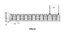
- back grinding operation S 8the back surface of the wafer 10 is ground using a grinding tool (not shown) to remove a predetermined thickness of the wafer 10 , as illustrated in FIG. 3I .
- This back grindingmakes the wafer 10 thinner, leading to a reduction in the thickness of the semiconductor device 100 .
- dicing operation S 9the resulting structure is diced using a dicing tool 30 to separate the first semiconductor dies 110 of the wafer 10 from one another, as illustrated in FIG. 3J .
- the encapsulant 140is also diced to provide a number of semiconductor devices. In each of the semiconductor devices, the side surfaces as well as the back surface of the first semiconductor die 110 are exposed to the outside.
- FIG. 4there is illustrated a cross-sectional view of a semiconductor device 200 according to another embodiment of the present invention.
- the semiconductor device 200comprises a first semiconductor die 210 formed with through-silicon vias 215 , a plurality of second semiconductor dies 120 stacked on the first semiconductor die 210 , a plurality of conductive connection members 130 , an encapsulant 140 , a plurality of redistribution layers 250 and a plurality of solder balls 260 .
- the first semiconductor die 210has an approximately planar first surface 211 , an approximately planar second surface 212 opposed to the first surface 211 , and approximately planar third surfaces 213 substantially perpendicular to the first surface 211 and the second surface 212 . Further, the first semiconductor die 210 includes a plurality of bond pads 214 formed on the first surface 211 thereof. Each of the through-silicon vias 215 of the first semiconductor die 210 penetrates the bond pad 214 formed on the first surface 211 and extends to the second surface 212 . The through-silicon vias 215 serve to electrically connect the first semiconductor die 210 to an external device (not shown), thereby eliminating the need for additional conductive wires to electrically connect the first semiconductor die 210 to the external device.
- the through-silicon vias 215are formed by forming through-holes penetrating the first semiconductor die 210 using a laser and plating the through-holes with a material selected from gold (Au), silver (Ag), copper (Cu), aluminum (Al), nickel (Ni), tungsten (W) and equivalents thereof. There is no restriction on the method and material for the formation of the through-silicon vias 215 .
- the second semiconductor dies 120 , the conductive connection members 130 and the encapsulant 140are the same as those of the semiconductor device 100 , and their explanation is omitted.
- the redistribution layers (RDL) 250are electrically connected to the through-silicon vias 215 of the first semiconductor die 210 . Specifically, the redistribution layers 250 are formed on the second surface 212 of the first semiconductor die 210 and are electrically connected to the through-silicon vias 215 .
- the redistribution layers 250can be formed in a fan-in and/or fan-out pattern to ensure a relatively large pitch between the solder balls 260 . Specifically, the redistribution layers 250 can be formed at positions closer to the inside and/or outside than the positions of the bond pads 214 .
- solder balls 260are attached to the respective redistribution layers 250 .
- the solder balls 260are regions on which an external device is mounted. Accordingly, the solder balls 260 serve to deliver electrical signals between the semiconductor device 200 and the external device.
- FIG. 5there is illustrated a flow chart of a method for fabricating a semiconductor device according to another embodiment of the present invention.
- the methodcomprises the following operations: preparation of wafer (S 11 ), connection of second semiconductor dies (S 12 ), encapsulation (S 13 ), grinding (S 14 ), repetition of electrical connection/encapsulation/grinding (S 15 ), back grinding (S 16 ), formation of redistribution layers (S 17 ), attachment of solder balls (S 18 ), and dicing (S 19 ).
- FIGS. 6A through 6Jthere are illustrated cross-sectional views for explaining the method. Some have already been explained above and description thereof is minimized here.
- a wafer 20is prepared in which a plurality of first semiconductor dies 210 are arranged, as illustrated in FIG. 6A .
- Each of the first semiconductor dies 210includes a plurality of bond pads 214 , and is formed with through-silicon vias 215 penetrating the bond pads 214 and extending to a predetermined depth thereof.
- second semiconductor dies 120 formed with through-silicon vias 125are electrically connected to the respective first semiconductor dies 210 of the wafer 20 , as illustrated in FIG. 6B .
- conductive connection members 130are interposed between the bond pads 214 of the first semiconductor dies 210 and the bond pads 124 of the second semiconductor dies 120 .
- the through-silicon vias 215 of the first semiconductor dies 210are electrically interconnected to the through-silicon vias 125 of the second semiconductor dies 120 .
- encapsulation operation S 13the second semiconductor dies 120 are encapsulated by an encapsulant 140 , as illustrated in FIG. 6C .
- the encapsulant 140completely encapsulates the second semiconductor dies 120 on the wafer 20 so as not to be exposed to the outside.
- grinding operation S 14a portion of the encapsulant 140 formed on the second semiconductor dies 120 is ground using a grinding tool to allow the upper surfaces of the second semiconductor dies 120 to be exposed to the outside, as illustrated in FIG. 6D .
- additional second semiconductor dies 120are electrically connected, encapsulated and ground, and this procedure is repeated one or more times to form stacks of the plurality of second semiconductor dies 120 .
- the electrical connection of the second semiconductor dies 120is achieved by the use of additional conductive connection members 130 .
- FIG. 6Fshows three-layer stacks of the second semiconductor dies 120 and the encapsulant 140 on the respective first semiconductor dies 210 , it should be understood that one, two, four or more layers of the second semiconductor dies 120 and the encapsulant 140 may be stacked on the respective first semiconductor dies 210 .
- back grinding operation S 16the back surface of the wafer 20 is ground using a grinding tool to remove a predetermined thickness of the wafer 20 , as illustrated in FIG. 6G .
- the wafer 20is back-ground in such a manner that the through-silicon vias 215 of the wafer 20 are exposed to the outside through the back surface of the wafer 20 .
- redistribution layers 250are formed on the back surface of the wafer 20 , as illustrated in FIG. 6H .
- the redistribution layers 250are electrically connected to the through-silicon vias 215 exposed to the outside through the back surface of the wafer 20 .
- the redistribution layers 250can be formed in a fan-in and/or fan-out pattern, but there is no restriction on the pattern of the redistribution layers 250 .
- solder balls 260are attached to the respective redistribution layers 250 formed on the back surface of the wafer 20 , as illustrated in FIG. 6I .
- dicing operation S 19the resulting structure is diced using a dicing tool 30 to separate the first semiconductor dies 210 of the wafer 20 from one another, as illustrated in FIG. 6J .
- the encapsulant 140is also diced to provide a number of semiconductor devices. In each of the semiconductor devices, the side surfaces as well as the back surface of the first semiconductor die 210 are exposed to the outside.
Landscapes
- Engineering & Computer Science (AREA)
- Microelectronics & Electronic Packaging (AREA)
- Power Engineering (AREA)
- Computer Hardware Design (AREA)
- Physics & Mathematics (AREA)
- Condensed Matter Physics & Semiconductors (AREA)
- General Physics & Mathematics (AREA)
- Manufacturing & Machinery (AREA)
- Internal Circuitry In Semiconductor Integrated Circuit Devices (AREA)
Abstract
Description
Claims (13)
Priority Applications (1)
| Application Number | Priority Date | Filing Date | Title |
|---|---|---|---|
| US12/270,690US7843052B1 (en) | 2008-11-13 | 2008-11-13 | Semiconductor devices and fabrication methods thereof |
Applications Claiming Priority (1)
| Application Number | Priority Date | Filing Date | Title |
|---|---|---|---|
| US12/270,690US7843052B1 (en) | 2008-11-13 | 2008-11-13 | Semiconductor devices and fabrication methods thereof |
Publications (1)
| Publication Number | Publication Date |
|---|---|
| US7843052B1true US7843052B1 (en) | 2010-11-30 |
Family
ID=43215613
Family Applications (1)
| Application Number | Title | Priority Date | Filing Date |
|---|---|---|---|
| US12/270,690ActiveUS7843052B1 (en) | 2008-11-13 | 2008-11-13 | Semiconductor devices and fabrication methods thereof |
Country Status (1)
| Country | Link |
|---|---|
| US (1) | US7843052B1 (en) |
Cited By (53)
| Publication number | Priority date | Publication date | Assignee | Title |
|---|---|---|---|---|
| US20080176611A1 (en)* | 2007-01-22 | 2008-07-24 | William Frederick Ryann | Garment securable mobile device |
| US20110156233A1 (en)* | 2009-12-31 | 2011-06-30 | Hynix Semiconductor Inc. | Stack package |
| US20110159638A1 (en)* | 2009-12-31 | 2011-06-30 | Meng-Jen Wang | Method for Making a Chip Package |
| US20110159639A1 (en)* | 2009-12-31 | 2011-06-30 | Kuo-Chung Yee | Method for Making a Stackable Package |
| US20110285014A1 (en)* | 2010-05-20 | 2011-11-24 | Advanced Semiconductor Engineering, Inc. | Packaging structure and package process |
| US20120007251A1 (en)* | 2010-07-08 | 2012-01-12 | National Tsing Hua University | Stacked multi-chip |
| US20120181673A1 (en)* | 2009-08-21 | 2012-07-19 | Stats Chippac, Ltd. | Semiconductor Device and Method of Stacking Die on Leadframe Electrically Connected by Conductive Pillars |
| US8324511B1 (en) | 2010-04-06 | 2012-12-04 | Amkor Technology, Inc. | Through via nub reveal method and structure |
| US8390130B1 (en) | 2011-01-06 | 2013-03-05 | Amkor Technology, Inc. | Through via recessed reveal structure and method |
| US8487445B1 (en) | 2010-10-05 | 2013-07-16 | Amkor Technology, Inc. | Semiconductor device having through electrodes protruding from dielectric layer |
| US20130217181A1 (en)* | 2011-07-07 | 2013-08-22 | Samsung-Electro-Mechanics Co., Ltd. | Method of manufacturing semiconductor package |
| US8552548B1 (en) | 2011-11-29 | 2013-10-08 | Amkor Technology, Inc. | Conductive pad on protruding through electrode semiconductor device |
| US20140001652A1 (en)* | 2012-06-29 | 2014-01-02 | Taiwan Semiconductor Manufacturing Company, Ltd. | Package-on-package structure having polymer-based material for warpage control |
| US8791501B1 (en) | 2010-12-03 | 2014-07-29 | Amkor Technology, Inc. | Integrated passive device structure and method |
| US20150069609A1 (en)* | 2013-09-12 | 2015-03-12 | International Business Machines Corporation | 3d chip crackstop |
| KR20150044329A (en)* | 2013-10-16 | 2015-04-24 | 삼성전자주식회사 | chip stacked semiconductor package and manufacturing method thereof |
| US9048298B1 (en) | 2012-03-29 | 2015-06-02 | Amkor Technology, Inc. | Backside warpage control structure and fabrication method |
| US9129943B1 (en) | 2012-03-29 | 2015-09-08 | Amkor Technology, Inc. | Embedded component package and fabrication method |
| WO2015138359A1 (en)* | 2014-03-10 | 2015-09-17 | Deca Technologies Inc. | Semiconductor device and method comprising thickened redistribution layers |
| US9159672B1 (en) | 2010-08-02 | 2015-10-13 | Amkor Technology, Inc. | Through via connected backside embedded circuit features structure and method |
| US9177926B2 (en) | 2011-12-30 | 2015-11-03 | Deca Technologies Inc | Semiconductor device and method comprising thickened redistribution layers |
| US9240380B2 (en) | 2009-08-21 | 2016-01-19 | Stats Chippac, Ltd. | Semiconductor device and method of forming interposer frame over semiconductor die to provide vertical interconnect |
| US9257413B2 (en) | 2013-08-29 | 2016-02-09 | SK Hynix Inc. | Stack packages including diffusion barriers over sidewalls of through via electrodes and methods of manufacturing the same |
| WO2016160948A1 (en)* | 2015-03-31 | 2016-10-06 | Qualcomm Incorporated | Stacked package configurations and methods of making the same |
| US9576919B2 (en) | 2011-12-30 | 2017-02-21 | Deca Technologies Inc. | Semiconductor device and method comprising redistribution layers |
| US9613830B2 (en) | 2011-12-30 | 2017-04-04 | Deca Technologies Inc. | Fully molded peripheral package on package device |
| US9704843B2 (en)* | 2012-08-02 | 2017-07-11 | Infineon Technologies Ag | Integrated system and method of making the integrated system |
| US9831170B2 (en) | 2011-12-30 | 2017-11-28 | Deca Technologies, Inc. | Fully molded miniaturized semiconductor module |
| US20180019178A1 (en)* | 2016-07-12 | 2018-01-18 | Industrial Technology Research Institute | Chip packaging and composite system board |
| US20180047702A1 (en)* | 2010-08-26 | 2018-02-15 | Intel Corporation | Bumpless build-up layer package with a pre-stacked microelectronic devices |
| US9934998B2 (en) | 2011-05-12 | 2018-04-03 | STATS ChipPAC Pte. Ltd. | Semiconductor device and method of singulating thin semiconductor wafer on carrier along modified region within non-active region formed by irradiating energy |
| US10050004B2 (en) | 2015-11-20 | 2018-08-14 | Deca Technologies Inc. | Fully molded peripheral package on package device |
| US10157803B2 (en) | 2016-09-19 | 2018-12-18 | Deca Technologies Inc. | Semiconductor device and method of unit specific progressive alignment |
| US10373870B2 (en) | 2010-02-16 | 2019-08-06 | Deca Technologies Inc. | Semiconductor device and method of packaging |
| US10573601B2 (en) | 2016-09-19 | 2020-02-25 | Deca Technologies Inc. | Semiconductor device and method of unit specific progressive alignment |
| US10672624B2 (en) | 2011-12-30 | 2020-06-02 | Deca Technologies Inc. | Method of making fully molded peripheral package on package device |
| USRE48111E1 (en) | 2009-08-21 | 2020-07-21 | JCET Semiconductor (Shaoxing) Co. Ltd. | Semiconductor device and method of forming interposer frame over semiconductor die to provide vertical interconnect |
| CN111710660A (en)* | 2014-05-27 | 2020-09-25 | 美光科技公司 | Interconnect structure with redundant electrical connectors and related systems and methods |
| US11056453B2 (en) | 2019-06-18 | 2021-07-06 | Deca Technologies Usa, Inc. | Stackable fully molded semiconductor structure with vertical interconnects |
| US11276676B2 (en)* | 2018-05-15 | 2022-03-15 | Invensas Bonding Technologies, Inc. | Stacked devices and methods of fabrication |
| US20230091513A1 (en)* | 2020-05-19 | 2023-03-23 | Shanghai Xianfang Semiconductor Co., Ltd. | Wafer-level chip structure, multiple-chip stacked and interconnected structure and fabricating method thereof |
| US11652083B2 (en) | 2017-05-11 | 2023-05-16 | Adeia Semiconductor Bonding Technologies Inc. | Processed stacked dies |
| US11658173B2 (en) | 2016-05-19 | 2023-05-23 | Adeia Semiconductor Bonding Technologies Inc. | Stacked dies and methods for forming bonded structures |
| US11764189B2 (en) | 2018-07-06 | 2023-09-19 | Adeia Semiconductor Bonding Technologies Inc. | Molded direct bonded and interconnected stack |
| US11817409B2 (en) | 2019-01-14 | 2023-11-14 | Adeia Semiconductor Bonding Technologies Inc. | Directly bonded structures without intervening adhesive and methods for forming the same |
| US11955463B2 (en) | 2019-06-26 | 2024-04-09 | Adeia Semiconductor Bonding Technologies Inc. | Direct bonded stack structures for increased reliability and improved yield in microelectronics |
| US12046569B2 (en) | 2020-06-30 | 2024-07-23 | Adeia Semiconductor Bonding Technologies Inc. | Integrated device packages with integrated device die and dummy element |
| US12046482B2 (en) | 2018-07-06 | 2024-07-23 | Adeia Semiconductor Bonding Technologies, Inc. | Microelectronic assemblies |
| US12080672B2 (en) | 2019-09-26 | 2024-09-03 | Adeia Semiconductor Bonding Technologies Inc. | Direct gang bonding methods including directly bonding first element to second element to form bonded structure without adhesive |
| US12176294B2 (en) | 2020-09-04 | 2024-12-24 | Adeia Semiconductor Bonding Technologies, Inc. | Bonded structure with interconnect structure |
| US12322718B2 (en) | 2020-09-04 | 2025-06-03 | Adeia Semiconductor Bonding Technologies Inc. | Bonded structure with interconnect structure |
| US12374656B2 (en) | 2017-06-15 | 2025-07-29 | Adeia Semiconductor Bonding Technologies Inc. | Multi-chip modules formed using wafer-level processing of a reconstituted wafer |
| US12438065B2 (en) | 2021-07-01 | 2025-10-07 | Deca Technologies Usa, Inc. | Fully molded semiconductor structure with through silicon via (TSV) vertical interconnects |
Citations (20)
| Publication number | Priority date | Publication date | Assignee | Title |
|---|---|---|---|---|
| US4394712A (en) | 1981-03-18 | 1983-07-19 | General Electric Company | Alignment-enhancing feed-through conductors for stackable silicon-on-sapphire wafers |
| US4499655A (en) | 1981-03-18 | 1985-02-19 | General Electric Company | Method for making alignment-enhancing feed-through conductors for stackable silicon-on-sapphire |
| US5229647A (en) | 1991-03-27 | 1993-07-20 | Micron Technology, Inc. | High density data storage using stacked wafers |
| US6168969B1 (en) | 1996-02-16 | 2001-01-02 | Micron Technology, Inc. | Surface mount IC using silicon vias in an area array format or same size as die array |
| US20020017710A1 (en) | 2000-08-04 | 2002-02-14 | Seiko Epson Corporation | Semiconductor device and method of manufacturing the same, circuit board, and electronic equipment |
| US6379982B1 (en) | 2000-08-17 | 2002-04-30 | Micron Technology, Inc. | Wafer on wafer packaging and method of fabrication for full-wafer burn-in and testing |
| US6429509B1 (en) | 1999-05-03 | 2002-08-06 | United Microelectronics Corporation | Integrated circuit with improved interconnect structure and process for making same |
| US6448661B1 (en) | 2001-02-09 | 2002-09-10 | Samsung Electornics Co., Ltd. | Three-dimensional multi-chip package having chip selection pads and manufacturing method thereof |
| US6573461B2 (en) | 2001-09-20 | 2003-06-03 | Dpac Technologies Corp | Retaining ring interconnect used for 3-D stacking |
| US6577013B1 (en) | 2000-09-05 | 2003-06-10 | Amkor Technology, Inc. | Chip size semiconductor packages with stacked dies |
| US6780770B2 (en) | 2000-12-13 | 2004-08-24 | Medtronic, Inc. | Method for stacking semiconductor die within an implanted medical device |
| US20040192033A1 (en) | 2003-01-15 | 2004-09-30 | Kazumi Hara | Semiconductor device, method of manufacturing the same, circuit board, and electronic instrument |
| US20040251554A1 (en) | 2003-03-27 | 2004-12-16 | Seiko Epson Corporation | Semiconductor device, circuit board, electronic instrument, and method of manufacturing semiconductor device |
| US6853572B1 (en) | 2003-02-28 | 2005-02-08 | Virage Logic Corporation | Methods and apparatuses for a ROM memory array having twisted source or bit lines |
| US20050046002A1 (en) | 2003-08-26 | 2005-03-03 | Kang-Wook Lee | Chip stack package and manufacturing method thereof |
| US6873054B2 (en) | 2002-04-24 | 2005-03-29 | Seiko Epson Corporation | Semiconductor device and a method of manufacturing the same, a circuit board and an electronic apparatus |
| US20050104181A1 (en)* | 2003-11-19 | 2005-05-19 | Kang-Wook Lee | Wafer level stack structure for system-in-package and method thereof |
| US7151009B2 (en)* | 2004-06-18 | 2006-12-19 | Samsung Electronics Co., Ltd. | Method for manufacturing wafer level chip stack package |
| US20070007639A1 (en)* | 2005-06-24 | 2007-01-11 | Motohiko Fukazawa | Semiconductor device, manufacturing method for semiconductor device, and electronic equipment |
| US7223634B2 (en) | 2003-07-31 | 2007-05-29 | Seiko Epson Corporation | Semiconductor device, method for manufacturing the same, circuit board, and electronic apparatus |
- 2008
- 2008-11-13USUS12/270,690patent/US7843052B1/enactiveActive
Patent Citations (22)
| Publication number | Priority date | Publication date | Assignee | Title |
|---|---|---|---|---|
| US4499655A (en) | 1981-03-18 | 1985-02-19 | General Electric Company | Method for making alignment-enhancing feed-through conductors for stackable silicon-on-sapphire |
| US4394712A (en) | 1981-03-18 | 1983-07-19 | General Electric Company | Alignment-enhancing feed-through conductors for stackable silicon-on-sapphire wafers |
| US5229647A (en) | 1991-03-27 | 1993-07-20 | Micron Technology, Inc. | High density data storage using stacked wafers |
| US6168969B1 (en) | 1996-02-16 | 2001-01-02 | Micron Technology, Inc. | Surface mount IC using silicon vias in an area array format or same size as die array |
| US6429509B1 (en) | 1999-05-03 | 2002-08-06 | United Microelectronics Corporation | Integrated circuit with improved interconnect structure and process for making same |
| US6608371B2 (en)* | 2000-08-04 | 2003-08-19 | Seiko Epson Corporation | Semiconductor device and method of manufacturing the same, circuit board, and electronic equipment |
| US20020017710A1 (en) | 2000-08-04 | 2002-02-14 | Seiko Epson Corporation | Semiconductor device and method of manufacturing the same, circuit board, and electronic equipment |
| US6379982B1 (en) | 2000-08-17 | 2002-04-30 | Micron Technology, Inc. | Wafer on wafer packaging and method of fabrication for full-wafer burn-in and testing |
| US6577013B1 (en) | 2000-09-05 | 2003-06-10 | Amkor Technology, Inc. | Chip size semiconductor packages with stacked dies |
| US6780770B2 (en) | 2000-12-13 | 2004-08-24 | Medtronic, Inc. | Method for stacking semiconductor die within an implanted medical device |
| US6448661B1 (en) | 2001-02-09 | 2002-09-10 | Samsung Electornics Co., Ltd. | Three-dimensional multi-chip package having chip selection pads and manufacturing method thereof |
| US6573461B2 (en) | 2001-09-20 | 2003-06-03 | Dpac Technologies Corp | Retaining ring interconnect used for 3-D stacking |
| US6873054B2 (en) | 2002-04-24 | 2005-03-29 | Seiko Epson Corporation | Semiconductor device and a method of manufacturing the same, a circuit board and an electronic apparatus |
| US20040192033A1 (en) | 2003-01-15 | 2004-09-30 | Kazumi Hara | Semiconductor device, method of manufacturing the same, circuit board, and electronic instrument |
| US6853572B1 (en) | 2003-02-28 | 2005-02-08 | Virage Logic Corporation | Methods and apparatuses for a ROM memory array having twisted source or bit lines |
| US20040251554A1 (en) | 2003-03-27 | 2004-12-16 | Seiko Epson Corporation | Semiconductor device, circuit board, electronic instrument, and method of manufacturing semiconductor device |
| US7208838B2 (en) | 2003-03-27 | 2007-04-24 | Seiko Epson Corporation | Semiconductor device, circuit board, and electronic instrument suitable for stacking and having a through hole |
| US7223634B2 (en) | 2003-07-31 | 2007-05-29 | Seiko Epson Corporation | Semiconductor device, method for manufacturing the same, circuit board, and electronic apparatus |
| US20050046002A1 (en) | 2003-08-26 | 2005-03-03 | Kang-Wook Lee | Chip stack package and manufacturing method thereof |
| US20050104181A1 (en)* | 2003-11-19 | 2005-05-19 | Kang-Wook Lee | Wafer level stack structure for system-in-package and method thereof |
| US7151009B2 (en)* | 2004-06-18 | 2006-12-19 | Samsung Electronics Co., Ltd. | Method for manufacturing wafer level chip stack package |
| US20070007639A1 (en)* | 2005-06-24 | 2007-01-11 | Motohiko Fukazawa | Semiconductor device, manufacturing method for semiconductor device, and electronic equipment |
Non-Patent Citations (1)
| Title |
|---|
| Park et al., "Semiconductor Package and Fabricating Method Thereof", U.S. Appl. No. 12/190,039, filed Aug. 12, 2008. |
Cited By (100)
| Publication number | Priority date | Publication date | Assignee | Title |
|---|---|---|---|---|
| US20080176611A1 (en)* | 2007-01-22 | 2008-07-24 | William Frederick Ryann | Garment securable mobile device |
| US8868143B2 (en)* | 2007-01-22 | 2014-10-21 | William Frederick Ryann | Garment securable mobile device |
| US20120181673A1 (en)* | 2009-08-21 | 2012-07-19 | Stats Chippac, Ltd. | Semiconductor Device and Method of Stacking Die on Leadframe Electrically Connected by Conductive Pillars |
| USRE48408E1 (en) | 2009-08-21 | 2021-01-26 | Jcet Semiconductor (Shaoxing) Co., Ltd. | Semiconductor device and method of forming interposer frame over semiconductor die to provide vertical interconnect |
| US9893045B2 (en) | 2009-08-21 | 2018-02-13 | STATS ChipPAC Pte. Ltd. | Semiconductor device and method of forming interposer frame over semiconductor die to provide vertical interconnect |
| USRE48111E1 (en) | 2009-08-21 | 2020-07-21 | JCET Semiconductor (Shaoxing) Co. Ltd. | Semiconductor device and method of forming interposer frame over semiconductor die to provide vertical interconnect |
| US9177901B2 (en)* | 2009-08-21 | 2015-11-03 | Stats Chippac, Ltd. | Semiconductor device and method of stacking die on leadframe electrically connected by conductive pillars |
| US9240380B2 (en) | 2009-08-21 | 2016-01-19 | Stats Chippac, Ltd. | Semiconductor device and method of forming interposer frame over semiconductor die to provide vertical interconnect |
| US8110910B2 (en)* | 2009-12-31 | 2012-02-07 | Hynix Semiconductor Inc. | Stack package |
| US8252629B2 (en)* | 2009-12-31 | 2012-08-28 | Advanced Semiconductor Engineering, Inc. | Method for making a stackable package |
| US20110159639A1 (en)* | 2009-12-31 | 2011-06-30 | Kuo-Chung Yee | Method for Making a Stackable Package |
| US20110159638A1 (en)* | 2009-12-31 | 2011-06-30 | Meng-Jen Wang | Method for Making a Chip Package |
| US20110156233A1 (en)* | 2009-12-31 | 2011-06-30 | Hynix Semiconductor Inc. | Stack package |
| US8691625B2 (en)* | 2009-12-31 | 2014-04-08 | Advanced Semiconductor Engineering, Inc. | Method for making a chip package |
| US10373870B2 (en) | 2010-02-16 | 2019-08-06 | Deca Technologies Inc. | Semiconductor device and method of packaging |
| US8324511B1 (en) | 2010-04-06 | 2012-12-04 | Amkor Technology, Inc. | Through via nub reveal method and structure |
| US9324614B1 (en) | 2010-04-06 | 2016-04-26 | Amkor Technology, Inc. | Through via nub reveal method and structure |
| US8258007B2 (en)* | 2010-05-20 | 2012-09-04 | Advanced Semiconductor Engineering, Inc. | Package process |
| US20110285014A1 (en)* | 2010-05-20 | 2011-11-24 | Advanced Semiconductor Engineering, Inc. | Packaging structure and package process |
| US20120007251A1 (en)* | 2010-07-08 | 2012-01-12 | National Tsing Hua University | Stacked multi-chip |
| US8174126B2 (en)* | 2010-07-08 | 2012-05-08 | National Tsing Hua University | Stacked multi-chip |
| US9159672B1 (en) | 2010-08-02 | 2015-10-13 | Amkor Technology, Inc. | Through via connected backside embedded circuit features structure and method |
| US20180047702A1 (en)* | 2010-08-26 | 2018-02-15 | Intel Corporation | Bumpless build-up layer package with a pre-stacked microelectronic devices |
| US8900995B1 (en) | 2010-10-05 | 2014-12-02 | Amkor Technology, Inc. | Semiconductor device and manufacturing method thereof |
| US8487445B1 (en) | 2010-10-05 | 2013-07-16 | Amkor Technology, Inc. | Semiconductor device having through electrodes protruding from dielectric layer |
| US8791501B1 (en) | 2010-12-03 | 2014-07-29 | Amkor Technology, Inc. | Integrated passive device structure and method |
| US9082833B1 (en) | 2011-01-06 | 2015-07-14 | Amkor Technology, Inc. | Through via recessed reveal structure and method |
| US8390130B1 (en) | 2011-01-06 | 2013-03-05 | Amkor Technology, Inc. | Through via recessed reveal structure and method |
| US9934998B2 (en) | 2011-05-12 | 2018-04-03 | STATS ChipPAC Pte. Ltd. | Semiconductor device and method of singulating thin semiconductor wafer on carrier along modified region within non-active region formed by irradiating energy |
| US9496219B2 (en) | 2011-07-07 | 2016-11-15 | Samsung Electro-Mechanics Co., Ltd. | Semiconductor package including an antenna formed in a groove within a sealing element |
| US20130217181A1 (en)* | 2011-07-07 | 2013-08-22 | Samsung-Electro-Mechanics Co., Ltd. | Method of manufacturing semiconductor package |
| US10410967B1 (en) | 2011-11-29 | 2019-09-10 | Amkor Technology, Inc. | Electronic device comprising a conductive pad on a protruding-through electrode |
| US11043458B2 (en) | 2011-11-29 | 2021-06-22 | Amkor Technology Singapore Holding Pte. Ltd. | Method of manufacturing an electronic device comprising a conductive pad on a protruding-through electrode |
| US8981572B1 (en) | 2011-11-29 | 2015-03-17 | Amkor Technology, Inc. | Conductive pad on protruding through electrode semiconductor device |
| US8552548B1 (en) | 2011-11-29 | 2013-10-08 | Amkor Technology, Inc. | Conductive pad on protruding through electrode semiconductor device |
| US9947623B1 (en) | 2011-11-29 | 2018-04-17 | Amkor Technology, Inc. | Semiconductor device comprising a conductive pad on a protruding-through electrode |
| US9431323B1 (en) | 2011-11-29 | 2016-08-30 | Amkor Technology, Inc. | Conductive pad on protruding through electrode |
| US10672624B2 (en) | 2011-12-30 | 2020-06-02 | Deca Technologies Inc. | Method of making fully molded peripheral package on package device |
| US9831170B2 (en) | 2011-12-30 | 2017-11-28 | Deca Technologies, Inc. | Fully molded miniaturized semiconductor module |
| US9576919B2 (en) | 2011-12-30 | 2017-02-21 | Deca Technologies Inc. | Semiconductor device and method comprising redistribution layers |
| US9613830B2 (en) | 2011-12-30 | 2017-04-04 | Deca Technologies Inc. | Fully molded peripheral package on package device |
| US9177926B2 (en) | 2011-12-30 | 2015-11-03 | Deca Technologies Inc | Semiconductor device and method comprising thickened redistribution layers |
| US10373902B2 (en) | 2011-12-30 | 2019-08-06 | Deca Technologies Inc. | Fully molded miniaturized semiconductor module |
| US9048298B1 (en) | 2012-03-29 | 2015-06-02 | Amkor Technology, Inc. | Backside warpage control structure and fabrication method |
| US9129943B1 (en) | 2012-03-29 | 2015-09-08 | Amkor Technology, Inc. | Embedded component package and fabrication method |
| US10014240B1 (en) | 2012-03-29 | 2018-07-03 | Amkor Technology, Inc. | Embedded component package and fabrication method |
| US11133285B2 (en)* | 2012-06-29 | 2021-09-28 | Taiwan Semiconductor Manufacturing Company, Ltd. | Package-on-package structure having polymer-based material for warpage control |
| US20140001652A1 (en)* | 2012-06-29 | 2014-01-02 | Taiwan Semiconductor Manufacturing Company, Ltd. | Package-on-package structure having polymer-based material for warpage control |
| US9627355B2 (en) | 2012-06-29 | 2017-04-18 | Taiwan Semiconductor Manufacturing Co., Ltd. | Package-on-package structure having polymer-based material for warpage control |
| CN103515326B (en)* | 2012-06-29 | 2017-04-12 | 台湾积体电路制造股份有限公司 | Package-on-package structure having polymer-based material for warpage control |
| CN103515326A (en)* | 2012-06-29 | 2014-01-15 | 台湾积体电路制造股份有限公司 | Package-on-package structure having polymer-based material for warpage control |
| US9349663B2 (en)* | 2012-06-29 | 2016-05-24 | Taiwan Semiconductor Manufacturing Co., Ltd. | Package-on-package structure having polymer-based material for warpage control |
| US10269763B2 (en) | 2012-06-29 | 2019-04-23 | Taiwan Semiconductor Manufacturing Co., Ltd. | Package-on-package structure having polymer-based material for warpage control |
| US10224317B2 (en) | 2012-08-02 | 2019-03-05 | Infineon Technologies Ag | Integrated system and method of making the integrated system |
| US9704843B2 (en)* | 2012-08-02 | 2017-07-11 | Infineon Technologies Ag | Integrated system and method of making the integrated system |
| US9257413B2 (en) | 2013-08-29 | 2016-02-09 | SK Hynix Inc. | Stack packages including diffusion barriers over sidewalls of through via electrodes and methods of manufacturing the same |
| US20150069609A1 (en)* | 2013-09-12 | 2015-03-12 | International Business Machines Corporation | 3d chip crackstop |
| KR102143518B1 (en) | 2013-10-16 | 2020-08-11 | 삼성전자 주식회사 | chip stacked semiconductor package and manufacturing method thereof |
| CN104576621B (en)* | 2013-10-16 | 2018-07-24 | 三星电子株式会社 | Chip stacks semiconductor package assembly and a manufacturing method thereof |
| KR20150044329A (en)* | 2013-10-16 | 2015-04-24 | 삼성전자주식회사 | chip stacked semiconductor package and manufacturing method thereof |
| US9905538B2 (en)* | 2013-10-16 | 2018-02-27 | Samsung Electronics Co., Ltd. | Chip-stacked semiconductor package and method of manufacturing the same |
| WO2015138359A1 (en)* | 2014-03-10 | 2015-09-17 | Deca Technologies Inc. | Semiconductor device and method comprising thickened redistribution layers |
| CN111710660A (en)* | 2014-05-27 | 2020-09-25 | 美光科技公司 | Interconnect structure with redundant electrical connectors and related systems and methods |
| CN111710660B (en)* | 2014-05-27 | 2024-01-26 | 美光科技公司 | Interconnect structures with redundant electrical connectors and related systems and methods |
| CN107431065B (en)* | 2015-03-31 | 2019-10-01 | 高通股份有限公司 | Stacked package configuration and its manufacturing method |
| WO2016160948A1 (en)* | 2015-03-31 | 2016-10-06 | Qualcomm Incorporated | Stacked package configurations and methods of making the same |
| US9799628B2 (en) | 2015-03-31 | 2017-10-24 | Qualcomm Incorporated | Stacked package configurations and methods of making the same |
| CN107431065A (en)* | 2015-03-31 | 2017-12-01 | 高通股份有限公司 | Stacked package configures and its manufacture method |
| US10050004B2 (en) | 2015-11-20 | 2018-08-14 | Deca Technologies Inc. | Fully molded peripheral package on package device |
| US12266650B2 (en) | 2016-05-19 | 2025-04-01 | Adeia Semiconductor Bonding Technologies Inc. | Stacked dies and methods for forming bonded structures |
| US11658173B2 (en) | 2016-05-19 | 2023-05-23 | Adeia Semiconductor Bonding Technologies Inc. | Stacked dies and methods for forming bonded structures |
| US12113056B2 (en) | 2016-05-19 | 2024-10-08 | Adeia Semiconductor Bonding Technologies Inc. | Stacked dies and methods for forming bonded structures |
| US11837596B2 (en) | 2016-05-19 | 2023-12-05 | Adeia Semiconductor Bonding Technologies Inc. | Stacked dies and methods for forming bonded structures |
| US20180019178A1 (en)* | 2016-07-12 | 2018-01-18 | Industrial Technology Research Institute | Chip packaging and composite system board |
| US10490478B2 (en)* | 2016-07-12 | 2019-11-26 | Industrial Technology Research Institute | Chip packaging and composite system board |
| US10157803B2 (en) | 2016-09-19 | 2018-12-18 | Deca Technologies Inc. | Semiconductor device and method of unit specific progressive alignment |
| US10573601B2 (en) | 2016-09-19 | 2020-02-25 | Deca Technologies Inc. | Semiconductor device and method of unit specific progressive alignment |
| US11652083B2 (en) | 2017-05-11 | 2023-05-16 | Adeia Semiconductor Bonding Technologies Inc. | Processed stacked dies |
| US12068278B2 (en) | 2017-05-11 | 2024-08-20 | Adeia Semiconductor Bonding Technologies Inc. | Processed stacked dies |
| US12374656B2 (en) | 2017-06-15 | 2025-07-29 | Adeia Semiconductor Bonding Technologies Inc. | Multi-chip modules formed using wafer-level processing of a reconstituted wafer |
| US11276676B2 (en)* | 2018-05-15 | 2022-03-15 | Invensas Bonding Technologies, Inc. | Stacked devices and methods of fabrication |
| US11916054B2 (en) | 2018-05-15 | 2024-02-27 | Adeia Semiconductor Bonding Technologies Inc. | Stacked devices and methods of fabrication |
| US12401011B2 (en) | 2018-05-15 | 2025-08-26 | Adeia Semiconductor Bonding Technologies Inc. | Stacked devices and methods of fabrication |
| US12347820B2 (en) | 2018-05-15 | 2025-07-01 | Adeia Semiconductor Bonding Technologies Inc. | Stacked devices and methods of fabrication |
| US11837582B2 (en) | 2018-07-06 | 2023-12-05 | Adeia Semiconductor Bonding Technologies Inc. | Molded direct bonded and interconnected stack |
| US12046482B2 (en) | 2018-07-06 | 2024-07-23 | Adeia Semiconductor Bonding Technologies, Inc. | Microelectronic assemblies |
| US11764189B2 (en) | 2018-07-06 | 2023-09-19 | Adeia Semiconductor Bonding Technologies Inc. | Molded direct bonded and interconnected stack |
| US12341025B2 (en) | 2018-07-06 | 2025-06-24 | Adeia Semiconductor Bonding Technologies Inc. | Microelectronic assemblies |
| US12266640B2 (en) | 2018-07-06 | 2025-04-01 | Adeia Semiconductor Bonding Technologies Inc. | Molded direct bonded and interconnected stack |
| US11817409B2 (en) | 2019-01-14 | 2023-11-14 | Adeia Semiconductor Bonding Technologies Inc. | Directly bonded structures without intervening adhesive and methods for forming the same |
| US11056453B2 (en) | 2019-06-18 | 2021-07-06 | Deca Technologies Usa, Inc. | Stackable fully molded semiconductor structure with vertical interconnects |
| US12261140B2 (en) | 2019-06-18 | 2025-03-25 | Deca Technologies Usa, Inc. | Stackable fully molded semiconductor structure with vertical interconnects |
| US12272677B2 (en) | 2019-06-26 | 2025-04-08 | Adeia Semiconductor Bonding Technologies Inc. | Direct bonded stack structures for increased reliability and improved yield in microelectronics |
| US11955463B2 (en) | 2019-06-26 | 2024-04-09 | Adeia Semiconductor Bonding Technologies Inc. | Direct bonded stack structures for increased reliability and improved yield in microelectronics |
| US12080672B2 (en) | 2019-09-26 | 2024-09-03 | Adeia Semiconductor Bonding Technologies Inc. | Direct gang bonding methods including directly bonding first element to second element to form bonded structure without adhesive |
| US20230091513A1 (en)* | 2020-05-19 | 2023-03-23 | Shanghai Xianfang Semiconductor Co., Ltd. | Wafer-level chip structure, multiple-chip stacked and interconnected structure and fabricating method thereof |
| US12046569B2 (en) | 2020-06-30 | 2024-07-23 | Adeia Semiconductor Bonding Technologies Inc. | Integrated device packages with integrated device die and dummy element |
| US12322718B2 (en) | 2020-09-04 | 2025-06-03 | Adeia Semiconductor Bonding Technologies Inc. | Bonded structure with interconnect structure |
| US12176294B2 (en) | 2020-09-04 | 2024-12-24 | Adeia Semiconductor Bonding Technologies, Inc. | Bonded structure with interconnect structure |
| US12438065B2 (en) | 2021-07-01 | 2025-10-07 | Deca Technologies Usa, Inc. | Fully molded semiconductor structure with through silicon via (TSV) vertical interconnects |
Similar Documents
| Publication | Publication Date | Title |
|---|---|---|
| US7843052B1 (en) | Semiconductor devices and fabrication methods thereof | |
| US11961742B2 (en) | Semiconductor device and manufacturing method thereof | |
| US11158587B2 (en) | Packaged semiconductor devices, methods of packaging semiconductor devices, and PoP devices | |
| TWI875458B (en) | Semiconductor device and manufacturing method thereof | |
| TWI819767B (en) | Semiconductor package and fabricating method thereof | |
| KR101806596B1 (en) | Fan-out package and methods of forming thereof | |
| CN106558537B (en) | Integrated multi-output structure and forming method | |
| US9761568B2 (en) | Thin fan-out multi-chip stacked packages and the method for manufacturing the same | |
| US9030019B2 (en) | Semiconductor device and method of manufacture thereof | |
| US7687318B2 (en) | Extended redistribution layers bumped wafer | |
| US20180130769A1 (en) | Substrate Based Fan-Out Wafer Level Packaging | |
| US11424199B2 (en) | Connector formation methods and packaged semiconductor devices | |
| US10714403B2 (en) | Semiconductor device package with patterned conductive layers and an interconnecting structure | |
| CN104051383A (en) | Packaged semiconductor device, method of packaging semiconductor device, and PoP device | |
| KR20170019298A (en) | Semiconductor package and fabricating method thereof | |
| CN116895540A (en) | Semiconductor device and method of forming embedded redistribution layer | |
| KR20230026958A (en) | Split rdl connection between die and ubm | |
| US20190259731A1 (en) | Substrate based fan-out wafer level packaging | |
| US20180130720A1 (en) | Substrate Based Fan-Out Wafer Level Packaging | |
| US20250096095A1 (en) | Semiconductor Device and Methods of Making and Using Dummy Vias to Reduce Short-Circuits Between Solder Bumps | |
| KR20240000682A (en) | Semiconductor package and method for manufacturing the semiconductor package | |
| TWI885507B (en) | Semiconductor package and fabricating method thereof | |
| KR20240164742A (en) | Semiconductor device and method of making a fan-out semiconductor package with pre-assembled passive modules | |
| CN119890140A (en) | Semiconductor device and method for manufacturing double-sided bridge die package structure |
Legal Events
| Date | Code | Title | Description |
|---|---|---|---|
| AS | Assignment | Owner name:AMKOR TECHNOLOGY, INC., ARIZONA Free format text:ASSIGNMENT OF ASSIGNORS INTEREST;ASSIGNORS:YOO, MIN;LEE, KI WOOK;LEE, MIN JAE;REEL/FRAME:021831/0752 Effective date:20081111 | |
| AS | Assignment | Owner name:BANK OF AMERICA, N.A., TEXAS Free format text:PATENT SECURITY AGREEMENT;ASSIGNOR:AMKOR TECHNOLOGY, INC.;REEL/FRAME:022764/0864 Effective date:20090416 | |
| STCF | Information on status: patent grant | Free format text:PATENTED CASE | |
| AS | Assignment | Owner name:BANK OF AMERICA, N.A., TEXAS Free format text:PATENT SECURITY AGREEMENT;ASSIGNOR:AMKOR TECHNOLOGY, INC.;REEL/FRAME:029422/0178 Effective date:20120913 | |
| FPAY | Fee payment | Year of fee payment:4 | |
| MAFP | Maintenance fee payment | Free format text:PAYMENT OF MAINTENANCE FEE, 8TH YEAR, LARGE ENTITY (ORIGINAL EVENT CODE: M1552) Year of fee payment:8 | |
| AS | Assignment | Owner name:BANK OF AMERICA, N.A., AS AGENT, CALIFORNIA Free format text:SECURITY INTEREST;ASSIGNOR:AMKOR TECHNOLOGY, INC.;REEL/FRAME:046683/0139 Effective date:20180713 | |
| AS | Assignment | Owner name:AMKOR TECHNOLOGY SINGAPORE HOLDING PTE.LTD., SINGAPORE Free format text:ASSIGNMENT OF ASSIGNORS INTEREST;ASSIGNOR:AMKOR TECHNOLOGY, INC.;REEL/FRAME:054067/0135 Effective date:20191119 | |
| MAFP | Maintenance fee payment | Free format text:PAYMENT OF MAINTENANCE FEE, 12TH YEAR, LARGE ENTITY (ORIGINAL EVENT CODE: M1553); ENTITY STATUS OF PATENT OWNER: LARGE ENTITY Year of fee payment:12 |