US7839097B2 - System and method for wide-range high-accuracy-low-dropout current regulation - Google Patents
System and method for wide-range high-accuracy-low-dropout current regulationDownload PDFInfo
- Publication number
- US7839097B2 US7839097B2US12/012,394US1239408AUS7839097B2US 7839097 B2US7839097 B2US 7839097B2US 1239408 AUS1239408 AUS 1239408AUS 7839097 B2US7839097 B2US 7839097B2
- Authority
- US
- United States
- Prior art keywords
- node
- terminal
- fet
- electrically coupled
- current
- Prior art date
- Legal status (The legal status is an assumption and is not a legal conclusion. Google has not performed a legal analysis and makes no representation as to the accuracy of the status listed.)
- Active, expires
Links
- 238000000034methodMethods0.000titleclaimsdescription7
- 230000001105regulatory effectEffects0.000claimsabstractdescription7
- 230000008878couplingEffects0.000claimsdescription8
- 238000010168coupling processMethods0.000claimsdescription8
- 238000005859coupling reactionMethods0.000claimsdescription8
- 230000005669field effectEffects0.000claimsdescription7
- 239000004065semiconductorSubstances0.000abstractdescription5
- 238000010586diagramMethods0.000description6
- 229910001416lithium ionInorganic materials0.000description2
- 230000004075alterationEffects0.000description1
- 230000008859changeEffects0.000description1
- 230000006870functionEffects0.000description1
- 229910044991metal oxideInorganic materials0.000description1
- 150000004706metal oxidesChemical class0.000description1
- 238000012986modificationMethods0.000description1
- 230000004048modificationEffects0.000description1
- 230000001737promoting effectEffects0.000description1
Images


Classifications
- H—ELECTRICITY
- H05—ELECTRIC TECHNIQUES NOT OTHERWISE PROVIDED FOR
- H05B—ELECTRIC HEATING; ELECTRIC LIGHT SOURCES NOT OTHERWISE PROVIDED FOR; CIRCUIT ARRANGEMENTS FOR ELECTRIC LIGHT SOURCES, IN GENERAL
- H05B45/00—Circuit arrangements for operating light-emitting diodes [LED]
- H05B45/40—Details of LED load circuits
- H05B45/44—Details of LED load circuits with an active control inside an LED matrix
- H05B45/46—Details of LED load circuits with an active control inside an LED matrix having LEDs disposed in parallel lines
- G—PHYSICS
- G05—CONTROLLING; REGULATING
- G05F—SYSTEMS FOR REGULATING ELECTRIC OR MAGNETIC VARIABLES
- G05F3/00—Non-retroactive systems for regulating electric variables by using an uncontrolled element, or an uncontrolled combination of elements, such element or such combination having self-regulating properties
- G05F3/02—Regulating voltage or current
- G05F3/08—Regulating voltage or current wherein the variable is DC
- G05F3/10—Regulating voltage or current wherein the variable is DC using uncontrolled devices with non-linear characteristics
- G05F3/16—Regulating voltage or current wherein the variable is DC using uncontrolled devices with non-linear characteristics being semiconductor devices
Definitions
- the present inventionrelates generally to semiconductor integrated circuits (IC) and the like.
- the inventionrelates to a unique LED driving circuit which maintains a high current accuracy over wide range of current changes while keeping a low voltage drop.
- power controlincludes voltage or current regulation.
- One very popular example that requires constant current controlis the light emitting diode (LED) application.
- LEDlight emitting diode
- the LED unitAs a lighting source, the LED unit is required to work with wide range brightness, which is proportional with the forward current passing through the LED unit. Therefore, the LED current needs to be tightly regulated throughout a wide range of current changes.
- the driving voltagewhich is at the battery voltage, can be dropped to merely 100 mV above the backlighting LED voltage, leaving very low voltage “headroom” for the constant current control. This makes it difficult to directly drive the LED without stepping up the input voltage.
- FIG. 1is a schematic diagram illustrating a typical current sink circuit used to control white LED current according to the prior art.
- the circuitis coupled between a voltage source represented by node 11 and node 12 .
- the current source 13 and resistor 15are coupled in series.
- the input terminal 17 of a non-inverting operational amplifier (NOA) 16is coupled to the node 14 between the current source 13 and the resistor 15 .
- the output terminal 19 of the NOA 16is coupled to the gate terminal 20 A of a field effect transistor (FET) 20 .
- a light emitting diode (LED) 21is coupled between the node 11 and the drain terminal 20 B of the FET 20 .
- a resistor 24is coupled between the node 12 and the source terminal 20 C of the FET 20 .
- the feedback terminal 18 of the NOA 16is coupled to the node 23 .
- the non-inverting input voltage (Vref 1 ) of the NOA 16i.e., the voltage at node 14
- resistor (R 1 ) 15a function of resistor (R 1 ) 15 .
- V ref1V — R 2 +Vos, (1)
- Vosis the offset voltage of the NOA 16 .
- What is desiredis a circuit to maintain high current accuracy over wide range of current while keeping the voltage “headroom” very low.
- the circuit for driving one or more light emitting diode (LED) devicescomprises a first and a second nodes which are adapted to be electrically coupled to a source of voltage, a constant current source and a first resistance means coupled in series between the first node and the second node, a third node coupled between the constant current source and the first resistance means, one or more driving units coupled together in parallel.
- LEDlight emitting diode
- Each of the driving unitscomprises a noninverting operational amplifier (NOA) with its input terminal electrically coupled to the third node, a first field effect transistor (FET) with its gate terminal coupled to the NOA's output terminal, an LED coupled between the first node and a drain terminal of the first FET, a current sense resistance means coupled between a source terminal of the first FET and the second node, and a fourth node between the current sense resistance means and the source terminal of the first FET.
- the fourth nodeis coupled to a feedback terminal of the NOA.
- the NOA's non-inverting input voltageremains constant while the electrical current passing through the LED is regulated by regulating the current sense resistance means.
- the present inventionalso teaches a method for maintaining high current accuracy over wide range of current passing through a light emitting diode (LED) while keeping low voltage drop for a current regulation driving circuit coupled to a voltage source.
- the driving circuitincludes a driving component, an LED, and resistance means coupled together through various nodes.
- the driving componentincludes a noninverting operational amplifier (NOA) coupled to a first field effect transistor (FET), the driving component's first terminal being coupled to the NOA's input terminal, the NOA's output terminal being coupled to the first FET's gate terminal, the driving component's second terminal being coupled to the first FET's drain terminal, the driving component's third terminal being coupled both to the NOA's feedback terminal and to the first FET's source terminal.
- the methodincludes the steps of:
- the first resistance meanscan be implemented as an NMOS FET, and the current sense resistance means can be implemented as an array of NMOS FETs electrically coupled together in parallel.
- FIG. 1is a schematic diagram illustrating a circuit for driving an LED according to the prior art
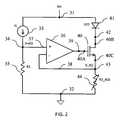
- FIG. 2is a schematic diagram illustrating a circuit for driving an LED according to the present invention
- FIG. 3is a schematic diagram illustrating a circuit for driving an LED according to one preferred embodiment of the present invention.
- FIG. 4is a schematic diagram illustrating a multiple-channel circuit for driving multiple LEDs according to another preferred embodiment of the present invention.
- FIG. 2is a schematic circuit diagram illustrating a semiconductor circuit according to the typical embodiment of the present invention.
- the circuitis electrically coupled between a voltage source represented by node 31 and node 32 .
- a constant current source 33 and resistance means 35are coupled in series between the voltage source represented by node 31 and node 32 .
- the input terminal 37 of a non-inverting operational amplifier (NOA) 36is electrically coupled to the node 34 between the constant current source 33 and the resistance means 35 .
- the output terminal 39 of the NOA 36is electrically coupled to the gate terminal 40 A of a field effect transistor (FET) 40 .
- a light emitting diode (LED) 41is coupled between the node 31 and the drain terminal 40 B of the FET 40 .
- NOAnon-inverting operational amplifier
- a current sense resistance means (R 2 _ADJ) 44is electrically coupled between the node 32 and the source terminal 40 C of the FET 40 .
- the feedback terminal 38 of the NOA 36is coupled to the node 43 .
- the NOA 36 and the FET 40constitute a driving component with three terminals represented by the input terminal 37 of the NOA 36 , the drain terminal 40 B of the FET 40 , and the source terminal 40 C of the FET 40 respectively, which are electrically coupled to node 34 , node 42 and node 43 respectively.
- the first current pathis through node 31 , constant current source 33 , node 34 , the resistance means 35 , and node 32 .
- a second current pathis through node 31 , LED 41 , node 42 , FET 40 , node 43 , the current sense resistance means 44 , and node 32 .
- the driving componentis electrically coupled between the two current paths.
- the circuit according to the present inventionadjusts the current sense resistor (R 2 _ADJ) 44 .
- the current source (I 1 ) 33remains constant at all time, keeping Vref 2 , i.e. the voltage at node 34 , at a fixed level that is close to Vref 1 in FIG. 1 in high current case.
- Vosmaintains a small percentage of the input signals, Vref 2 and V_R 2 , regardless of the LED current level.
- This circuitcan maintain high accuracy over the wide range of the LED current while keeping low voltage drop for the current sink circuitry.
- LED current2 mA ⁇ 20 mA
- Vos4 mV
- the resistance means (R 1 ) 35 in FIG. 2can be implemented as a negative-channel metal-oxide semiconductor (NMOS) on-resistance (Rdson) 55 as shown in FIG. 3 .
- the current resistance means (R 2 _ADJ) 44 in FIG. 2can be implemented as an array (M 1 , M 2 , . . . , MN) 64 of NMOS Rdson coupled together in parallel as illustrated in FIG. 3 .
- the first current pathis through the constant current source 53 , node 54 , and the resistance means 55 .
- a second current pathis through the LED 60 , node 61 , the driving component 62 , node 63 , and the current sense resistance means 64 .
- the driving component 62is electrically coupled between the two current paths, with its first terminal coupled to node 54 , the second terminal coupled to node 61 and the third terminal coupled to node 63 .
- the NMOS array 64includes at least two NMOS coupled together in parallel.
- the gate of the NMOS (M 0 ) 55is coupled to the voltage supply VCC and it works as a resistor.
- the gates of the NMOS array 64are controlled by a series of digital signals D 1 , D 2 , . . . , DN respectively.
- the controlled NMOSworks as a resistor.
- the digital signalis lower than a threshold, the controlled NMOS is turned off.
- the digital signals D 1 , D 2 , . . . , DNBy changing the digital signals D 1 , D 2 , . . . , DN, the overall resistance of the NMOS array 64 is adjusted, and the LED current is automatically changed accordingly.
- a multi-channel current regulation circuitcan be implemented in the form as illustrated in FIG. 4 .
- at least two driving units 81 - 82are coupled together in parallel.
- the configuration of each of the driving unitsis substantially same as the configuration as illustrated in FIG. 3 .
- the circuit within each dash-line blockdrives one LED. All the circuits share the same reference voltage Vref 2 generated by current source I 1 and NMOS (M 0 ) 75 .
- M 0is required to be physically and topologically close to M 1 , M 2 , . . . , MN.
- the NMOS FETs (M 0 , M 1 . . . MN)should also be the same type of the devices.
- the NMOS FETs (M 0 , M 1 . . . MN)are identical or substantially same devices.
Landscapes
- Physics & Mathematics (AREA)
- Engineering & Computer Science (AREA)
- Nonlinear Science (AREA)
- Electromagnetism (AREA)
- General Physics & Mathematics (AREA)
- Radar, Positioning & Navigation (AREA)
- Automation & Control Theory (AREA)
- Led Devices (AREA)
Abstract
Description
Vref1=V—R2+Vos, (1)
Wherein, Vos is the offset voltage of the
I_ADJ*R1=I_LED*R2+Vos, (2)
- (a) providing a first current path through a constant current source, a first node, and a first resistance means;
- (b) providing a second current path through the LED, a second node, a third node, and a current sense resistance means; and
- (c) coupling a driving component between the first current path and the second current path by:
- coupling the driving component's first terminal to the first node;
- coupling the driving component's second terminal to the second node; and
- coupling the driving component's third terminal to the third node;
- (d) adjusting the overall resistance of the current sense resistance means using a number of digital signals such that the electrical current passing through the LED varies while the voltage at the first node remains constant.
I1*R1=I_LED*R2_ADJ+Vos, (3)
Claims (3)
Priority Applications (1)
| Application Number | Priority Date | Filing Date | Title |
|---|---|---|---|
| US12/012,394US7839097B2 (en) | 2007-02-03 | 2008-01-31 | System and method for wide-range high-accuracy-low-dropout current regulation |
Applications Claiming Priority (2)
| Application Number | Priority Date | Filing Date | Title |
|---|---|---|---|
| US89931607P | 2007-02-03 | 2007-02-03 | |
| US12/012,394US7839097B2 (en) | 2007-02-03 | 2008-01-31 | System and method for wide-range high-accuracy-low-dropout current regulation |
Publications (2)
| Publication Number | Publication Date |
|---|---|
| US20080185975A1 US20080185975A1 (en) | 2008-08-07 |
| US7839097B2true US7839097B2 (en) | 2010-11-23 |
Family
ID=39675583
Family Applications (1)
| Application Number | Title | Priority Date | Filing Date |
|---|---|---|---|
| US12/012,394Active2028-06-23US7839097B2 (en) | 2007-02-03 | 2008-01-31 | System and method for wide-range high-accuracy-low-dropout current regulation |
Country Status (1)
| Country | Link |
|---|---|
| US (1) | US7839097B2 (en) |
Cited By (4)
| Publication number | Priority date | Publication date | Assignee | Title |
|---|---|---|---|---|
| US20110199008A1 (en)* | 2010-02-04 | 2011-08-18 | Austriamicrosystems Ag | Current source, current source arrangement and their use |
| US20120068619A1 (en)* | 2010-09-16 | 2012-03-22 | Samsung Electro-Mechanics Co., Ltd. | Device for controlling current of led |
| US9280165B2 (en)* | 2010-06-16 | 2016-03-08 | Autonetworks Technologies, Ltd. | Power supply control circuit using N-type and P-type FETs in parallel and power supply control device |
| US10921837B2 (en)* | 2015-10-15 | 2021-02-16 | SK Hynix Inc. | Voltage regulator and operating method thereof |
Families Citing this family (9)
| Publication number | Priority date | Publication date | Assignee | Title |
|---|---|---|---|---|
| US8160950B2 (en)* | 2002-11-08 | 2012-04-17 | Fx Alliance, Llc | Method and apparatus for trading assets |
| US8482216B1 (en) | 2009-04-01 | 2013-07-09 | Kinetic Technologies, Inc. | System and method for uniform control of current regulated outputs over wide voltage ranges |
| US20100283773A1 (en)* | 2009-05-08 | 2010-11-11 | Yong-Hun Kim | Driving integrated circuit and image display device including the same |
| CN102201203A (en)* | 2011-04-26 | 2011-09-28 | 苏州佳世达电通有限公司 | Electronic device and display using same |
| CN102256418B (en)* | 2011-07-15 | 2014-02-19 | 深圳市华星光电技术有限公司 | PWM (pulse width modulation) dimming circuit |
| TW201434344A (en)* | 2013-02-19 | 2014-09-01 | Princeton Technology Corp | LED driving device |
| CN103354083B (en)* | 2013-07-11 | 2015-06-17 | 京东方科技集团股份有限公司 | Backlight drive circuit and display device |
| US9411349B2 (en)* | 2013-11-14 | 2016-08-09 | Litelfuse, Inc. | Overcurrent detection of load circuits with temperature compensation |
| JP6311357B2 (en)* | 2014-03-05 | 2018-04-18 | 株式会社オートネットワーク技術研究所 | Prevention device |
Citations (9)
| Publication number | Priority date | Publication date | Assignee | Title |
|---|---|---|---|---|
| US5025204A (en)* | 1990-01-05 | 1991-06-18 | Hewlett-Packard Company | Current mirror using resistor ratios in CMOS process |
| US6538394B2 (en)* | 2001-03-30 | 2003-03-25 | Maxim Integrated Products, Inc. | Current source methods and apparatus for light emitting diodes |
| US20060022652A1 (en)* | 2004-07-27 | 2006-02-02 | Kazuhiko Nishimura | Regulator circuit capable of detecting variations in voltage |
| US20060186827A1 (en)* | 2005-02-11 | 2006-08-24 | Stmicroelectronics S.R.L. | Supply device of circuit branches with LED diodes |
| US20060202637A1 (en)* | 2005-03-08 | 2006-09-14 | Yung-Hsin Chiang | Driving circuit and method of tuning a driving voltage of a light-emitting device utilizing a feedback mechanism |
| US20070120506A1 (en)* | 2005-11-30 | 2007-05-31 | Semtech Corporation | High efficiency power supply for LED lighting applications |
| US20080174929A1 (en)* | 2007-01-24 | 2008-07-24 | Vastview Technology Inc. | Light emitting diode driver |
| US7456586B2 (en)* | 2006-01-31 | 2008-11-25 | Jabil Circuit, Inc. | Voltage controlled light source and image presentation device using the same |
| US7539538B2 (en)* | 2004-05-28 | 2009-05-26 | Boston Science Neuromodulation Corporation | Low power loss current digital-to-analog converter used in an implantable pulse generator |
- 2008
- 2008-01-31USUS12/012,394patent/US7839097B2/enactiveActive
Patent Citations (9)
| Publication number | Priority date | Publication date | Assignee | Title |
|---|---|---|---|---|
| US5025204A (en)* | 1990-01-05 | 1991-06-18 | Hewlett-Packard Company | Current mirror using resistor ratios in CMOS process |
| US6538394B2 (en)* | 2001-03-30 | 2003-03-25 | Maxim Integrated Products, Inc. | Current source methods and apparatus for light emitting diodes |
| US7539538B2 (en)* | 2004-05-28 | 2009-05-26 | Boston Science Neuromodulation Corporation | Low power loss current digital-to-analog converter used in an implantable pulse generator |
| US20060022652A1 (en)* | 2004-07-27 | 2006-02-02 | Kazuhiko Nishimura | Regulator circuit capable of detecting variations in voltage |
| US20060186827A1 (en)* | 2005-02-11 | 2006-08-24 | Stmicroelectronics S.R.L. | Supply device of circuit branches with LED diodes |
| US20060202637A1 (en)* | 2005-03-08 | 2006-09-14 | Yung-Hsin Chiang | Driving circuit and method of tuning a driving voltage of a light-emitting device utilizing a feedback mechanism |
| US20070120506A1 (en)* | 2005-11-30 | 2007-05-31 | Semtech Corporation | High efficiency power supply for LED lighting applications |
| US7456586B2 (en)* | 2006-01-31 | 2008-11-25 | Jabil Circuit, Inc. | Voltage controlled light source and image presentation device using the same |
| US20080174929A1 (en)* | 2007-01-24 | 2008-07-24 | Vastview Technology Inc. | Light emitting diode driver |
Cited By (6)
| Publication number | Priority date | Publication date | Assignee | Title |
|---|---|---|---|---|
| US20110199008A1 (en)* | 2010-02-04 | 2011-08-18 | Austriamicrosystems Ag | Current source, current source arrangement and their use |
| US8547030B2 (en)* | 2010-02-04 | 2013-10-01 | Ams Ag | Current source, current source arrangement and their use |
| US9280165B2 (en)* | 2010-06-16 | 2016-03-08 | Autonetworks Technologies, Ltd. | Power supply control circuit using N-type and P-type FETs in parallel and power supply control device |
| US20120068619A1 (en)* | 2010-09-16 | 2012-03-22 | Samsung Electro-Mechanics Co., Ltd. | Device for controlling current of led |
| US8525437B2 (en)* | 2010-09-16 | 2013-09-03 | Samsung Electro-Mechanics Co., Ltd. | Device for controlling current of LED |
| US10921837B2 (en)* | 2015-10-15 | 2021-02-16 | SK Hynix Inc. | Voltage regulator and operating method thereof |
Also Published As
| Publication number | Publication date |
|---|---|
| US20080185975A1 (en) | 2008-08-07 |
Similar Documents
| Publication | Publication Date | Title |
|---|---|---|
| US7839097B2 (en) | System and method for wide-range high-accuracy-low-dropout current regulation | |
| US7683553B2 (en) | LED current control circuits and methods | |
| US7307614B2 (en) | Light emitting diode driver circuit | |
| TWI491312B (en) | Load driving circuit and multi-load feedback circuit | |
| US8063585B2 (en) | Power supply system and method for the operation of an electrical load | |
| US8941325B2 (en) | Light emitting device array driver circuit and current splitter circuit and method of splitting current therefor | |
| US10721804B2 (en) | Light-emitting diode driving circuit | |
| US20020140378A1 (en) | Current source methods and apparatus for light emitting diodes | |
| US7804258B2 (en) | Circuit for providing an approximately constant resistance and/or current and method therefor | |
| US8742689B2 (en) | Light emitting diode driving apparatus | |
| US7728529B2 (en) | LED driver using a depletion mode transistor to serve as a current source | |
| US20080068066A1 (en) | High efficiency white LED drivers | |
| US7781983B1 (en) | Closed-loop feedback circuit for controlling LEDs | |
| US9961729B1 (en) | Trimming system and method for regulated current mirrors | |
| JP7530421B2 (en) | Light emitting device driving device and light emitting system | |
| US9706610B2 (en) | Driving circuits for light emitting elements | |
| US10601416B2 (en) | Gate drive device | |
| CN115148162B (en) | Drive circuit, backlight circuit and display panel | |
| US20130015780A1 (en) | Pwm dimming circuit | |
| CN111356257B (en) | LED driver circuit | |
| US9013118B2 (en) | LED control system with a constant reference current | |
| US20230397311A1 (en) | Led driving circuit and method for controlling a current distribution to an led string | |
| KR100448734B1 (en) | Low voltage Current driving circuit | |
| US20240275260A1 (en) | Regulator circuit | |
| JP2025002990A (en) | LOAD DRIVE DEVICE, LIGHTING DEVICE, AND VEHICLE |
Legal Events
| Date | Code | Title | Description |
|---|---|---|---|
| AS | Assignment | Owner name:CORPORATION KINETIC TECHNOLOGIES, INC., CALIFORNIA Free format text:ASSIGNMENT OF ASSIGNORS INTEREST;ASSIGNORS:CHEN, LU;SHUM, KIN EDWARD;REEL/FRAME:020793/0744 Effective date:20080326 | |
| STCF | Information on status: patent grant | Free format text:PATENTED CASE | |
| REMI | Maintenance fee reminder mailed | ||
| FPAY | Fee payment | Year of fee payment:4 | |
| SULP | Surcharge for late payment | ||
| AS | Assignment | Owner name:KINETIC TECHNOLOGIES, INC., CALIFORNIA Free format text:CORRECTIVE ASSIGNMENT TO CORRECT THE ASSIGNEE NAME PREVIOUSLY RECORDED AT REEL: 020793 FRAME: 0744. ASSIGNOR(S) HEREBY CONFIRMS THE ASSIGNMENT;ASSIGNORS:CHEN, LU;SHUM, KIN EDWARD;REEL/FRAME:039872/0151 Effective date:20080326 | |
| MAFP | Maintenance fee payment | Free format text:PAYMENT OF MAINTENANCE FEE, 8TH YR, SMALL ENTITY (ORIGINAL EVENT CODE: M2552) Year of fee payment:8 | |
| AS | Assignment | Owner name:KINETIC TECHNOLOGIES INTERNATIONAL HOLDINGS LP, CANADA Free format text:ASSIGNMENT OF ASSIGNORS INTEREST;ASSIGNOR:KINETIC TECHNOLOGIES;REEL/FRAME:059852/0228 Effective date:20210205 | |
| MAFP | Maintenance fee payment | Free format text:PAYMENT OF MAINTENANCE FEE, 12TH YR, SMALL ENTITY (ORIGINAL EVENT CODE: M2553); ENTITY STATUS OF PATENT OWNER: SMALL ENTITY Year of fee payment:12 | |
| AS | Assignment | Owner name:KINETIC TECHNOLOGIES INTERNATIONAL HOLDINGS LP, CANADA Free format text:ASSIGNMENT OF ASSIGNORS INTEREST;ASSIGNOR:KINETIC TECHNOLOGIES, INC.;REEL/FRAME:060511/0118 Effective date:20220613 |