US7838922B2 - Electronic device including trenches and discontinuous storage elements - Google Patents
Electronic device including trenches and discontinuous storage elementsDownload PDFInfo
- Publication number
- US7838922B2 US7838922B2US11/626,753US62675307AUS7838922B2US 7838922 B2US7838922 B2US 7838922B2US 62675307 AUS62675307 AUS 62675307AUS 7838922 B2US7838922 B2US 7838922B2
- Authority
- US
- United States
- Prior art keywords
- gate electrode
- trench
- storage elements
- discontinuous storage
- electronic device
- Prior art date
- Legal status (The legal status is an assumption and is not a legal conclusion. Google has not performed a legal analysis and makes no representation as to the accuracy of the status listed.)
- Expired - Fee Related, expires
Links
Images


Classifications
- B—PERFORMING OPERATIONS; TRANSPORTING
- B82—NANOTECHNOLOGY
- B82Y—SPECIFIC USES OR APPLICATIONS OF NANOSTRUCTURES; MEASUREMENT OR ANALYSIS OF NANOSTRUCTURES; MANUFACTURE OR TREATMENT OF NANOSTRUCTURES
- B82Y10/00—Nanotechnology for information processing, storage or transmission, e.g. quantum computing or single electron logic
- H—ELECTRICITY
- H10—SEMICONDUCTOR DEVICES; ELECTRIC SOLID-STATE DEVICES NOT OTHERWISE PROVIDED FOR
- H10B—ELECTRONIC MEMORY DEVICES
- H10B41/00—Electrically erasable-and-programmable ROM [EEPROM] devices comprising floating gates
- H10B41/30—Electrically erasable-and-programmable ROM [EEPROM] devices comprising floating gates characterised by the memory core region
- H—ELECTRICITY
- H10—SEMICONDUCTOR DEVICES; ELECTRIC SOLID-STATE DEVICES NOT OTHERWISE PROVIDED FOR
- H10B—ELECTRONIC MEMORY DEVICES
- H10B69/00—Erasable-and-programmable ROM [EPROM] devices not provided for in groups H10B41/00 - H10B63/00, e.g. ultraviolet erasable-and-programmable ROM [UVEPROM] devices
- H—ELECTRICITY
- H10—SEMICONDUCTOR DEVICES; ELECTRIC SOLID-STATE DEVICES NOT OTHERWISE PROVIDED FOR
- H10D—INORGANIC ELECTRIC SEMICONDUCTOR DEVICES
- H10D30/00—Field-effect transistors [FET]
- H10D30/01—Manufacture or treatment
- H10D30/021—Manufacture or treatment of FETs having insulated gates [IGFET]
- H10D30/0411—Manufacture or treatment of FETs having insulated gates [IGFET] of FETs having floating gates
- H—ELECTRICITY
- H10—SEMICONDUCTOR DEVICES; ELECTRIC SOLID-STATE DEVICES NOT OTHERWISE PROVIDED FOR
- H10D—INORGANIC ELECTRIC SEMICONDUCTOR DEVICES
- H10D30/00—Field-effect transistors [FET]
- H10D30/60—Insulated-gate field-effect transistors [IGFET]
- H10D30/68—Floating-gate IGFETs
- H10D30/681—Floating-gate IGFETs having only two programming levels
- H—ELECTRICITY
- H10—SEMICONDUCTOR DEVICES; ELECTRIC SOLID-STATE DEVICES NOT OTHERWISE PROVIDED FOR
- H10D—INORGANIC ELECTRIC SEMICONDUCTOR DEVICES
- H10D64/00—Electrodes of devices having potential barriers
- H10D64/01—Manufacture or treatment
- H10D64/031—Manufacture or treatment of data-storage electrodes
- H10D64/035—Manufacture or treatment of data-storage electrodes comprising conductor-insulator-conductor-insulator-semiconductor structures
Definitions
- the present inventionrelates to electronic devices and processes, and more particularly, to electronic devices including trenches and discontinuous storage elements and processes of forming and using the electronic devices.
- Floating gate nonvolatile memories(“FG NVM”) are conventional and are commonly used in many applications.
- the three most common types of programming mechanisms for FG NVMinclude Fowler-Nordheim tunneling, conventional hot carrier injection, and source-side injection.
- Fowler-Nordheim tunnelingis efficient but is very slow. Efficiency can be measured by dividing the number of carriers that enter a floating gate or one or more other storage elements divided by the number of carriers that enter a memory cell having the floating gate or the other storage element(s). The latter number can be approximated by using the product of the programming current and the programming time.
- Hot carrier injectioncan include conventional hot carrier injection and source-side injection. Both involve the generation of hot carriers, some of which are injected into the floating or the other storage element(s).
- conventional hot carrier injectionwhen using a floating gate, an electrical field is generated along a channel region of a memory cell. Within the channel region, the electrical field is the highest near the drain region. The electrical field accelerates carriers flowing within the channel region, such that, within the channel region, the carriers are traveling the fastest near the drain region. A small fraction of carriers collide with silicon or one or more other atoms within the channel region, redirecting the energetic carriers to the floating gate or other charge storage element(s). An electrical field generated by a control gate electrode can help inject some of that small fraction of the hot carriers into the floating gate.
- Conventional hot carrier injectionis inefficient and has high programming current.
- Source-side injectionis a popular compromise, with respect to efficiency and programming current, between Fowler-Nordheim tunneling and conventional hot carrier injection. With source-side injection, hot carriers are still generated, however, most of the hot carriers are generated within a portion of the channel region that is spaced apart from the drain region. Memory cells designed to be programmed by source-side injection are not without problems. Typically, the memory cells require one or more additional critical lithographic sequences and result in larger memory cells.
- High density floating gate memoriesare becoming more difficult to fabricate in commercial volumes.
- the thickness of the gate dielectric layerdecreases, the likelihood of a pinhole or other defect extending through the thickness of the gate dielectric layer increases.
- Such a defectcan cause an electrical short or leakage path between the substrate and the floating gate.
- the electrical short or leakage pathcan affect the voltage on the floating gate, and therefore, the memory cell may not be able to retain data.
- One or more materialsmay be used for the gate dielectric layer instead of silicon dioxide, however, such material(s) may have other issues, such as material compatibility with other materials used in the memory cell, require new equipment, increase manufacturing costs, etc.
- FIG. 1includes an illustration of a cross-sectional view of a portion of a workpiece after forming a protective layer.
- FIGS. 2 and 3include illustrations of a top view and a cross-sectional view, respectively, of the workpiece of FIG. 1 after forming trenches.
- FIG. 4includes an illustration of a cross-sectional view of a workpiece of FIGS. 2 and 3 after forming a charge storage stack including discontinuous storage elements and a layer of a gate electrode material.
- FIG. 5includes an illustration of a cross-sectional view of a workpiece of FIG. 4 after forming gate electrodes.
- FIGS. 6 and 7include illustrations of a top view and a cross-sectional view, respectively, of the workpiece of FIG. 5 after removing portions of the charge storage stack and forming insulating layers on exposed surfaces of the substrate and gate electrodes.
- FIG. 8includes an illustration of a cross-sectional view of a workpiece of FIGS. 6 and 7 after forming another layer of a gate electrode material.
- FIGS. 9 and 10include illustrations of a top view and a cross-sectional view, respectively, of the workpiece of FIG. 8 after forming additional gate electrodes.
- FIG. 11includes an illustration of a top view of the workpiece of FIGS. 9 and 10 after selectively doping portions of the substrate within the mesas and under bottoms of the trenches.
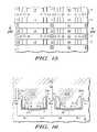
- FIGS. 12 and 13include illustrations of a top view and a cross-sectional view, respectively, of the workpiece of FIG. 11 after forming a substantially completed electronic device.
- FIG. 14includes an illustration of a top view of the workpiece of FIGS. 9 and 10 after selectively doping portions of the substrate within the mesas and under bottoms of the trenches in accordance with an alternative embodiment.
- FIGS. 15 and 16include illustrations of a top view and a cross-sectional view, respectively, of the workpiece of FIG. 14 after forming a substantially completed electronic device in accordance with the alternative embodiment.
- FIGS. 17 through 21include illustrations of the workpiece when forming buried bit lines and gate electrodes, wherein the some of the gate electrode are electrically connected to a gate line in accordance with an alternative embodiment.
- FIG. 22includes an illustration of a cross-sectional view of a workpiece of FIGS. 2 and 3 after forming a dielectric layer and a layer of a gate electrode material.
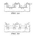
- FIG. 23includes an illustration of a cross-sectional view of a workpiece of FIG. 22 after forming gate electrodes and an insulating layer on exposed surfaces of the substrate and gate electrodes.
- FIG. 24includes an illustration of a cross-sectional view of a workpiece of FIG. 23 after forming a charge storage stack.
- FIG. 25include illustrations of a cross-sectional view of the workpiece of FIG. 24 after forming additional gate electrodes and removing exposed portions of the charge storage stack.
- FIGS. 26 through 32include circuit schematic diagrams, cross-sectional views of exemplary physical embodiments of the circuit schematic diagrams, and operating voltage tables for memory cell along a row within an NVM array.
- An electronic devicecan include a substrate including a trench having a bottom and a first wall.
- the electronic devicecan also include a first gate electrode within the trench and adjacent to the first wall and overlying the bottom of the trench, a second gate electrode overlying the substrate outside of the trench, and a third gate electrode within the trench and adjacent to the first gate electrode and overlying the bottom of the trench.
- the electronic devicecan also include discontinuous storage elements including a first set of discontinuous storage elements, wherein the first set of the discontinuous storage elements lies adjacent to the first wall of the trench. Processes of forming and using the electronic device are also described.
- the processes and structures describedallow memory cells or portions thereof to be formed with gate electrodes and doped regions adjacent to the gate electrodes that have dimensions smaller than the resolution limits of lithographic processes. Also, a set of gate electrodes is formed within and outside of each trench.
- the embodimentscan also be used to form three-transistor memory cells, which can allow for lower leakage current when the transistor is not being used (e.g., other memory cells being programmed or read, or the NVM array 18 is idling). Other embodiments described herein allow for an electronic device having a contactless array.
- discontinuous storage elementsis intended to mean spaced-apart objects capable of storing a charge.
- substantially all discontinuous storage elementsmay be initially formed and remain separate from one another.
- a substantially continuous layer of materialformed an later separated into discontinuous storage elements.
- substantially all discontinuous storage elementsmay be initially formed separate from one another, and later during the formation, some but not all of the discontinuous storage elements may coalesce.
- orientedis intended to mean a principal direction in which a feature extends (e.g., from a top view, the longer of two dimensions of the feature, such as the length). As between different features at the same elevation or at different elevations, the features may be oriented substantially parallel, substantially perpendicular, or another angular relationship with respect to each other.
- a nonvolatile memory stackcan include layers used to form at least part of a nonvolatile memory cell.
- a stackmay be part of a larger stack.
- a nonvolatile memory stackcan include a charge storage stack that is used to store charge within a nonvolatile memory cell.
- the terms “comprises,” “comprising,” “includes,” “including,” “has,” “having” or any other variation thereof,are intended to cover a non-exclusive inclusion.
- a process, method, article, or apparatus that comprises a list of elementsis not necessarily limited to only those elements but may include other elements not expressly listed or inherent to such process, method, article, or apparatus.
- “or”refers to an inclusive or and not to an exclusive or. For example, a condition A or B is satisfied by any one of the following: A is true (or present) and B is false (or not present), A is false (or not present) and B is true (or present), and both A and B are true (or present).
- FIG. 1includes a cross-sectional view of a portion of an electronic device 10 , such as an integrated circuit.
- the integrated circuitcan be a standalone memory, a microcontroller, or other integrated circuit that includes a memory.
- the electronic device 10can include a nonvolatile memory (“NVM”) array 18 , a portion of which is illustrated in FIG. 1 .
- a substrate 12can include a monocrystalline semiconductor wafer, a semiconductor-on-insulator wafer, a flat panel display (e.g., a silicon layer over a glass plate), or other substrate conventionally used to form electronic devices.
- shallow trench field isolationmay be formed over portions of the substrate 12 in peripheral areas outside of the NVM array 18 .
- the upper most surface of substrate 12is a primary surface 13 .
- the doping concentration of the substrate 12 along the primary surface 13 within the NVM array 18can be increased using a conventional or proprietary doping operation to potentially reduce leakage current between subsequently-formed gate electrodes that may overlie portions of the primary surface 13 .
- a protective layer 110can be formed over the primary surface 13 of the substrate 12 .
- the protective layer 110can include a pad layer 14 and an oxidation-resistant layer 16 over the pad layer 14 .
- the protective layer 110could have more or fewer layers than are illustrated.
- the protective layer 110can remain over the peripheral areas until fabrication of the NVM array 18 is substantially completed.
- the pad layer 14includes oxide
- the oxidation-resistant layer 16includes nitride.
- FIGS. 2 and 3include illustrations of a top view and a cross-sectional view, respectively, of the memory array after etching trenches 22 to define mesas 32 .
- a patterned resist layer(not illustrated), which includes openings at locations within the NVM array 18 where trenches are to be formed, is formed over the substrate 12 by a conventional or proprietary technique. Exposed portions of the protective layer 110 can then be removed by a conventional or proprietary technique to expose the primary surface 13 .
- the trenches 22are formed prior to removal of the patterned resist layer.
- the patterned resist layercan then be removed, and the trenches 22 can then be formed by a conventional or proprietary technique.
- the trenches 22extend from primary surface 13 and include bottoms 34 and walls 36 . Referring to FIG.
- the trenches 22are oriented substantially parallel to one another.
- the depths of trenches 22are in a range of approximately 50 to approximately 500 nm.
- the trenches 22are formed using a timed anisotropic etch to produce the walls 36 that are substantially vertical.
- the trenches 22have substantially uniform depths.
- the trenches 22are spaced apart from one another by the mesas 32 , which include remaining portions of the substrate 12 between the trenches 22 . After reading this specification, skilled artisans will appreciate that the trenches 22 can be shallower or deeper in other embodiments. Remaining portions of the protective layer 110 can be removed using a conventional or proprietary technique.
- a charge storage stack 48including a dielectric layer 42 , discontinuous storage elements 44 , and another dielectric layer 46 , can then be formed, as illustrated in FIG. 4 .
- the dielectric layer 42may be thermally grown using an oxidizing or nitridizing ambient, or deposited using a conventional or proprietary chemical vapor deposition technique, physical vapor deposition technique, atomic layer deposition technique, or a combination thereof.
- the dielectric layer 42can include one or more films of silicon dioxide, silicon nitride, silicon oxynitride, a high dielectric constant (“high-k”) material (e.g., dielectric constant greater than 8), or any combination thereof.
- high-khigh dielectric constant
- the high-k materialcan include Hf a O b N c , Hf a Si b O c , Hf a Si b O c N d , Hf a Zr b O c N d , Hf a Zr b Si c O d N e , Hf a Zr b O c , Zr a Si b O c , Zr a Si b O c N d , ZrO 2 , other Hf-containing or Zr-containing dielectric material, a doped version of any of the foregoing (lanthanum doped, niobium doped, etc.), or any combination thereof.
- the dielectric layer 42has a thickness in a range of approximately 1 to approximately 10 nm.
- the thickness and material selection of the dielectric layer 42will substantially determine its electrical properties. In one embodiment the thickness and material are chosen such that the dielectric layer 42 has a silicon dioxide equivalent thickness of less than 10 nm.
- discontinuous storage elements 44are then formed over NVM array 18 .
- discontinuous storage elements 44overlie the mesas 32 (including the primary surface 13 of the substrate 12 ) and lie within trenches 22 .
- the individual discontinuous storage elements 44are substantially physically separated from each other.
- the discontinuous storage elements 44can include a material capable of storing a charge, such as silicon, a nitride, a metal-containing material, another suitable material capable of storing charge, or any combination thereof.
- the discontinuous storage elements 44can include silicon nanocrystals or metal nanoclusters.
- a substantially continuous layer of amorphous siliconcan be formed over exposed surfaces of the substrate 12 .
- the substantially continuous layercan be exposed to heat or other processing conditions that can cause the layer to “ball up” or otherwise form silicon nanocrystals.
- the discontinuous storage elements 44may be undoped, doped during deposition, or doped after deposition.
- the discontinuous storage elements 44can be formed from one or more materials whose properties are not significantly adversely affected during a thermal oxidation process.
- a materialcan include platinum, palladium, iridium, osmium, ruthenium, rhenium, indium-tin, indium-zinc, aluminum-tin, or any combination thereof. Each of such materials, other than platinum and palladium, may form a conductive metal oxide.
- each of the discontinuous storage elements 44is no greater than approximately 10 nm in any dimension. In another embodiment, the discontinuous storage elements 44 can be larger, however, the discontinuous storage elements 44 are not formed so large as to form a continuous structure (i.e., all of the discontinuous storage elements 44 are not fused together).
- the dielectric layer 46is then formed over the discontinuous storage elements 44 .
- the dielectric layer 46can include one or more dielectric films, any of which may be thermally grown or deposited.
- the dielectric layer 46can include any one or more materials or be formed using any of the embodiments as described with respect to the dielectric 42 layer.
- the dielectric layer 46can have the same or different composition compared to the dielectric 42 layer and may be formed using the same or different formation technique compared to the dielectric layer 42 .
- a gate electrode material 50is then formed overlying the workpiece and only partly fills remaining portions of the trenches 22 , as illustrated in FIG. 4 .
- the gate electrode material 50can include a semiconductor-containing film, a metal-containing film, or any combination thereof.
- the gate electrode material 50includes polysilicon or amorphous silicon.
- the gate electrode material 50may include one or more other materials.
- the thickness of gate electrode material 50is not greater than approximately 200 nm, and in another particular embodiment is no greater than 90 nm.
- the thickness of gate electrode material 50is at least approximately 20 nm, and in another particular embodiment is at least 50 nm.
- the gate electrode material 50can have a dopant concentration of at least 1E19 atoms/cm 3 when gate electrode material 50 includes polysilicon or amorphous silicon.
- the gate electrode material 50can be deposited by chemical vapor deposition, physical vapor deposition, or a combination thereof. In an embodiment, the gate electrode material 50 can be deposited substantially conformally. In another embodiment, the gate electrode material 50 may not be completely conformal; however, a significant portion of the gate electrode material 50 still forms along the charge storage stack 48 near the walls 36 of the trenches 22 . In one particular embodiment, the gate electrode material 50 is doped when deposited, and in another particular embodiment, is doped after it is deposited.
- FIG. 5includes an illustration of a cross-sectional view after the gate electrode material 50 has been etched to form gate electrodes 52 .
- an anisotropic etchis performed to remove portions of gate electrode material 50 overlying the mesas 32 and portions of the bottoms of the trenches 22 .
- the gate electrodes 52are in the form of sidewall spacers and have an arc-shaped outer surface, although other shapes can be used in other embodiments.
- the bases of the gate electrodes 52have widths that are approximately the same as the thickness of the gate electrode material as deposited. In another embodiment, the bases have widths that are at least half of the thickness of the gate electrode material as deposited.
- each of the bases of the gate electrodes 52are in a range of approximately 50 to approximately 90 nm wide.
- the etching chemistry and other etching parameterscan use conventional or proprietary etching chemistries and etching parameters used for etching gate electrode materials.
- a mask and etch process sequencecan be used to separate the gate electrodes 52 at the ends of the trenches 22 , so that the gate electrodes 52 lying adjacent to opposite sides of the trenches 22 are not electrically shorted to each other. Portions of the charge storage stack 48 overlying the mesas 32 and lying between the gate electrodes 52 within the trenches 22 become exposed.
- FIGS. 6 and 7include illustrations of a top view and a cross-sectional view, respectively, after removing portions of the discontinuous storage elements 44 that are not protected by the gate electrodes 52 and remaining portions of the protective layer 110 .
- some dielectric or insulating layersare not illustrated to simplify understanding of positional relationships between features within NVM array 18 .
- the portions of the discontinuous storage elements 44can be removed by removing substantially all of the exposed portions of the charge storage stack 48 , removing part of the of the exposed portions of the charge storage stack 48 , thermally consuming (e.g., oxidizing or nitriding) the portions of the discontinuous storage elements 44 , or any combination thereof.
- the trenches 22 , the mesas 32 , and the gate electrodes 52are oriented substantially parallel to one another.
- substantially all of the exposed portions of the charge storage stack 48are removed.
- the dielectric layer 46 and the dielectric layer 42can be etched.
- the dielectric layer 42can be removed by a wet etch that undercuts discontinuous storage elements 44 , allowing them to be rinsed away.
- exposed portions of dielectric layer 46are removed, exposing discontinuous storage elements 44 , which can then undergo additional processing to convert them from an electrically conducting material to an electrically insulating material.
- discontinuous storage elements 44are silicon nanocrystals that are oxidized to form silicon dioxide.
- the discontinuous storage elements 44are etched, and the dielectric layer 42 remains.
- the protective layer 110is a sacrificial layer that is used to allow the gate electrodes 52 to include portions that extend above the primary surface 13 of the substrate 12 .
- the elevational difference between the primary surface 13 and the uppermost part of the gate electrodes 52is a function of the thicknesses of the protective layer 110 and the charge storage stack 48 . In a particular embodiment, the elevational difference is more strongly affected by the thickness of the protective layer 110 because the charge storage stack 48 is substantially thinner than the protective layer 110 .
- insulating layers 72are formed over portions of the substrate 12 within the trenches 22 and over the mesas 32 , and insulating layers 74 are formed along the exposed surfaces of the gate electrodes 52 .
- the insulating layers 72 and 74can include an oxide, a nitride, an oxynitride, or any combination thereof.
- the thickness of the insulating layers 72acts as an implant screen during a subsequent ion implantation when forming source/drain (“S/D”) regions.
- the insulating layer 74helps to protect the gate electrodes 52 during subsequent processing.
- the insulating layers 72 and 74can have a thickness in a range of approximately 5 to approximately 50 nm.
- the insulating layers 72 and 74can have the same composition or different compositions and the same thickness or different thicknesses.
- the insulating layers 72 and 74are formed by thermally oxidizing or nitriding parts of the substrate 12 and the gate electrodes 52 .
- an insulating layermay be deposited over the substrate 12 and gate electrodes 52 , wherein the insulating layer is formed in place of or in conjunction with the insulating layers 72 and 74 .
- the insulating layerhas a composition and thickness as previously described for the insulating layers 72 and 74 . Except as expressly recited herein, each of the insulating layers 72 and 74 , and the deposited insulating layer is formed using a conventional or proprietary technique.
- the gate electrode material 80can include any of the materials, thicknesses, and formation processes as described with respect to the gate electrode material 50 . As compared to the gate electrode material 50 , the gate electrode material 80 may have the same composition or different compositions, the same thickness, or different thicknesses, be formed using by repeating the same process technique or different process techniques, or any combination thereof.
- FIGS. 9 and 10include illustrations of a top view and a cross-sectional view, respectively, after the gate electrode material 80 has been etched to form gate electrodes 92 and 94 .
- an anisotropic etchis performed to remove portions of gate electrode material 80 overlying portions of the mesas 32 and the bottoms of the trenches 22 .
- each gate electrode 52has a gate electrode 92 along one side and a gate electrode 94 along the opposite side.
- the gate electrodes 92lie outside the trenches 22 and overlie the mesas 32 and the primary surface 13
- the gate electrodes 94overlie the bottoms of the trenches 22 .
- the gate electrodes 92 and 94are in the form of sidewall spacers and have an arc-shaped outer surface, although other shapes can be used in other embodiments.
- the bases of the gate electrodes 92 and 94have widths that are approximately the same as the thickness of the gate electrode material as deposited. In another embodiment, the bases have widths that are at least half of the thickness of the gate electrode material as deposited. In a particular embodiment, each of the bases of the gate electrodes 92 are in a range of approximately 50 to approximately 90 nm wide.
- the etching chemistry and other etching parameterscan use conventional or proprietary etching chemistries and etching parameters used for etching gate electrode materials.
- a mask and etch process sequencecan be used to separate the gate electrodes 94 at the end of the trenches 22 , so that the gate electrodes 94 lying adjacent to opposite sides of the trenches 22 are not electrically shorted to each other.
- FIGS. 11 to 13include a layout in which portions of the substrate 12 adjacent to the gate electrodes 92 and other portions of the substrate 12 adjacent to the gate electrodes are doped, and bit lines are oriented substantially perpendicular to the gate lines.
- a masking layeris formed over the array and includes masking members 112 and openings between the masking members 112 .
- the masking members 112are oriented substantially perpendicular to the gate members 52 , 92 , and 94 .
- a dopantis introduced into portions of the substrate between the masking members 112 to form doped regions 114 and 116 .
- the doped regions 114include portions of the substrate 12 within the mesas 32 , and the doped regions 116 include portions of the substrate 12 below the bottoms 34 of the trenches 22 .
- the doped regions 114 and 116can act as S/D regions.
- the dopantmay be a p-type dopant (e.g., boron) or an n-type dopant (e.g., phosphorus or arsenic).
- the dopantcan be introduced using ion implantation.
- the masking members 112are then removed by a conventional or proprietary technique.
- the implanted dopantis activated by one or more subsequent thermal cycles, which may or may not serve a different primary purpose such as oxidation, deposition, annealing, drive or activation of a different implant dopant.
- each of the doped regions 114 and 116has a dopant concentration of at least approximately 1E19 atoms/cm 3 .
- the formation of the masking members 112 , their subsequent removal, and doping to form the doped regions 114 and 116are performed using conventional of proprietary techniques.
- the NVM array 18is now substantially complete other than formation of the electrical connections. Component fabrication within peripheral areas (not illustrated) of the electronic device can be performed using one or more conventional or proprietary techniques.
- FIGS. 12 and 13include illustrations of a top view and a cross-sectional view, respectively, of a substantially completed electronic device.
- FIG. 12does not illustrate the insulating layers formed after forming the doped regions 114 and 116 to simplify understanding of the positional relationships between the conductive members (e.g., gate electrodes, doped regions, conductive lines, etc.) of the electronic device.
- FIG. 12includes conductive lines 122 and 124 that are oriented substantially perpendicular to the gate electrodes 52 , 92 , and 94 .
- the conductive lines 122 and 124are bit lines.
- the conductive lines 122are electrically connected to the doped regions 114 (within the mesas 32 ), and the conductive lines 124 are electrically connected to the doped regions 116 (below the bottoms of the trenches 22 ).
- FIG. 13includes a cross-sectional view at sectioning line 13 - 13 in FIG. 12 .
- the processis described with respect to FIG. 13 .
- An interlevel dielectric layer 1302is formed over the workpiece by a conventional or proprietary technique.
- the interlevel dielectric layer 1302is patterned to form contact openings that extend to doped regions 114 and 116 and to other portions of NVM array 18 that are not illustrated in FIGS. 12 and 13 .
- the interlevel dielectric layer 1302can include an insulating material, such as an oxide, a nitride, an oxynitride, or a combination thereof.
- an anisotropic etchcan be used to form contact openings.
- Conductive plugs 1304 and the conductive lines 122 and 124are then formed.
- the conductive plugs 1304 and the conductive lines 122 and 124can include the same or different conducting materials.
- Each of the conductive plugs 1304 and the conductive lines 122 and 124can include doped silicon, tungsten, titanium, tantalum, titanium nitride, tantalum nitride, aluminum, copper, another suitable conductive material, or any combination thereof.
- the conductive plugs 1304include tungsten
- the conductive lines 122 and 124include copper.
- An optional barrier layer, adhesion layer, or any combination thereofmay be formed before the corresponding conductive layers (e.g., tungsten for the conductive plugs 1304 and copper for the conductive lines 122 and 124 ).
- An optional capping layere.g., a metal-containing nitride may be used to encapsulate copper within the conductive lines 122 and 124 .
- the conductive plugs 1304are formed before the conductive lines 122 and 124 .
- a conductive layer(not illustrated) is formed over interlevel dielectric layer 1302 and substantially fills contact openings therein. Portions of the conductive layer that lie outside the contact openings are removed to form the conductive plugs 1304 .
- a conventional or proprietary chemical-mechanical polishing operationcan be performed, and in another embodiment, a conventional or proprietary etching process can be performed.
- Another insulating layer 1322is then deposited and patterned to form interconnect trenches where the conductive lines 122 and 124 are formed. Other interconnect trenches can be formed at locations within the NVM array 18 , outside the NVM array 18 , or any combination thereof.
- another conductive layeris formed over the interlevel dielectric layer 1302 and substantially fills the interconnect trenches in the insulating layer 1322 . Portions of the conductive layer that lie outside the interconnect trenches within the insulating layer 1322 are removed to form the conductive lines 122 and 124 .
- a conventional or proprietary chemical-mechanical polishing operationcan be performed, and in another embodiment, a conventional or proprietary etching process can be performed.
- the insulating layer 1322lies at substantially the same elevation as and between the conductive lines 122 and 124 .
- the conductive plugs 1302 and the conductive lines 122 and 124are formed concurrently using a conventional or proprietary dual-inlaid process.
- additional insulating and conductive layerscan be formed and patterned to form one or more additional levels of interconnects.
- an encapsulating layer 1342is formed over substrate 12 , including the NVM array 18 and peripheral areas.
- the encapsulating layer 1342can include one or more insulating film, such as an oxide, a nitride, an oxynitride, or a combination thereof.
- the NVM array 18includes memory cells 132 , 134 , 136 , and 138 , each of which is a three-transistor memory cell.
- FIGS. 14 to 16illustrate another embodiment having a different layout for the source/drain (“S/D”) regions and bit lines.
- FIGS. 14 to 16include a layout in which portions of the substrate 12 adjacent to the gate electrodes 92 and other portions of the substrate 12 adjacent to the gate electrodes 94 are doped, and other bit lines are oriented substantially parallel to the gate electrodes 52 , 92 , and 94 .
- the process through formation of the gate electrodes 92 and 94can be performed using any embodiment as previously described with respect to FIGS. 1 to 10 .
- a masking layeris formed over the array and includes masking members 142 and openings between the masking members 142 .
- the masking members 142cover portions of the mesas 32
- the masking members 142can cover portions of the gate electrodes 52 , 92 , and 94 but do not cover portions of the substrate 12 that lie under the bottoms 34 of the trenches 22 and between the gate electrodes 94 .
- a dopantis introduced into portions of the substrate 12 to form doped regions 144 and 146 .
- the doped regions 144include portions of the substrate 12 within the mesas 32
- the doped regions 146include portions of the substrate 12 below the bottoms of the trenches 22 .
- the doped regions 144 and 146can act as S/D regions.
- the doped region 146is oriented substantially parallel to the gate electrodes 52 , 92 , and 94 and acts as a bit line.
- the dopantmay be a p-type dopant (e.g., boron) or an n-type dopant (e.g., phosphorus or arsenic).
- the dopantcan be introduced using ion implantation.
- the masking members 142are then removed by a conventional or proprietary technique.
- the implanted dopantis activated by one or more subsequent thermal cycles, which may or may not serve a different primary purpose such as oxidation, deposition, annealing, drive or activation of a different implant dopant.
- each of doped regions 144 and 146has a dopant concentration of at least approximately 1E19 atoms/cm 3 .
- the formation of the masking members 142 , their subsequent removal, and doping to form the doped regions 144 and 146are performed using conventional of proprietary techniques.
- the NVM array 18is now substantially complete other than formation of the electrical connections. Component fabrication within peripheral areas (not illustrated) of the electronic device can be performed using one or more conventional or proprietary techniques.
- FIGS. 15 and 16include illustrations of a top view and a cross-sectional view, respectively, of a substantially completed electronic device.
- FIG. 15does not illustrate the insulating layers after forming the doped regions 144 and 146 to simplify understanding of the positional relationships between the conductive members (e.g., gate electrodes, doped regions, conductive lines, etc.) of the electronic device.
- FIG. 15includes conductive lines 152 that are oriented substantially perpendicular to the doped regions 146 and the gate electrodes 52 , 92 , and 94 .
- the conductive lines 152are bit lines.
- the conductive lines 152are electrically connected to the doped regions 144 (within the mesas 32 ). Portions of the mesas 32 that were not doped when forming the doped regions 144 are illustrated as mesas 32 in FIG. 15 .
- FIG. 16includes a cross-sectional view at sectioning line 16 - 16 in FIG. 15 .
- the processis described with respect to FIG. 16 .
- the process of forming the interlevel dielectric layer 1302 , conductive plugs 1304 , and insulating layer 1322 (not illustrated)are formed using any of the embodiments described with respect to FIGS. 12 and 13 .
- the insulating layer 1322is patterned to form interconnect trenches. Referring to FIG. 15 , the remaining portions (not illustrated) of the insulating layer 1322 lie between the conductive lines 152 , and the interconnect trenches lie where the conductive lines 152 are to be formed.
- the conductive lines 152are then formed.
- the conductive lines 152can include any of the materials as previously described with respect to the conductive plugs 1304 and the conductive lines 122 and 124 . More particularly, after the insulating layer 1322 is then deposited and patterned to form interconnect trenches, a conductive layer is formed over the interlevel dielectric layer 1302 and substantially fills the interconnect trenches in the insulating layer 1322 . Portions of the conductive layer that lie outside the interconnect trenches within the insulating layer 1322 are removed to form the conductive lines 152 . In one embodiment, a conventional or proprietary chemical-mechanical polishing operation can be performed, and in another embodiment, a conventional or proprietary etching process can be performed. The insulating layer 1322 lies at substantially the same elevation as and between the conductive lines 152 . In another embodiment (not illustrated), the conductive plugs 1302 and the conductive lines 152 are formed concurrently using a conventional or proprietary dual-inlaid process.
- additional insulating and conductive layerscan be formed and patterned to form one or more additional levels of interconnects.
- the encapsulating layer 1342is formed over substrate 12 , including the NVM array 18 and peripheral areas.
- the NVM array 18includes memory cells 162 , 164 , 166 , and 168 , each of which is a three-transistor memory cell.
- Another layoutcan be used in another embodiment (not illustrated).
- the masking, doping, and bit line orientations described with respect to FIGS. 14 to 16can be reversed.
- the doped regions 144can be continuous along the trenches, and the doped regions 146 can be segmented.
- the conductive lines 152would be electrically connected to the doped regions 146 , rather than the doped regions 144 .
- a spacer including a gate electrode materialcan be segmented into a plurality of gate electrodes to allow word lines, select lines, or other gate lines to be oriented substantially perpendicular to the trenches 22 .
- a workpieceis processed using any of the embodiments as described with respect to FIGS. 1 to 8 .
- the gate electrode material 80(in FIG. 8 ) is etched to form sidewall spacers 171 and 173 , as illustrated in FIG. 17 .
- the sidewall spacers 171 and 173have more of a squared-off shape as compared to the gate electrodes 92 and 94 in FIG. 9 .
- the etchis performed so that the insulating layers 74 between the sidewall spacers 171 and 173 are exposed, so that the sidewall spacers 171 and 173 are not electrically connected to each other.
- the sidewall spacers 171 and 173are formed using a conventional or proprietary processing technique. In a particular embodiment, the sidewall spacers 171 and 173 extend along substantially all of the lengths of the trenches 22 .
- FIG. 18includes an illustration of a top view after forming a patterned masking layer over the workpiece.
- a masking layeris deposited and patterned to define a masking member 181 .
- the masking member 181covers the sidewall spacers 171 and portions of the sidewall spacers 173 .
- the masking membercovers the sidewall spacers 173 and portions of the sidewall spacers 173 .
- the exposed portions of the sidewall spacers 173are etched.
- the sidewall spacer etchis selective to insulating layers. Therefore, the insulating layers 72 protect portions of the substrate 12 within the mesas 32 when the sidewall spacers 173 are etched.
- the masking member 181is then removed.
- the patterned masking layer formation, sidewall spacer etch, and patterned masking layer removalare performed using convention or proprietary processing operations.
- FIG. 19includes sidewall spacers 171 , which act as gate electrodes, and gate electrodes 191 , which are remaining portions of the sidewall spacers 173 .
- the gate electrodes 52act as control gate electrodes
- the sidewall spacers 171 and gate electrodes 191act as select gate electrodes.
- the gate electrodes 52 and sidewall spacers 171are substantially continuous along the walls of the trenches, and portions of the gate electrodes 52 are covered by the gate electrodes 191 .
- Doped regions 193are formed within the mesas 32
- doped regions 195are formed along the bottoms of the trenches 22 .
- the doped regions 193 and the doped regions 195act as source/drain regions and are formed using an embodiment previous described.
- the trenches 22 , the gate electrodes 52 , the sidewall spacers 171 , the doped regions 193 , and the doped regions 195are oriented substantially along the same direction.
- FIG. 20includes an illustration of the workpiece after forming insulating spacers 201 and 203 .
- the insulating spacers 201 and 203include different material and are formed when forming spacer structures in the logic regions (outside the NVM array 18 ).
- the insulating spacers 201can include an oxide, and the insulating spacers 203 can include a nitride. As illustrated, the two sides of the insulating spacers 203 merge in the middle of the trench 22 .
- a dep-etch-dep processcan be formed that preferentially fills in the lowest exposed portions of the trenches, while not forming a significant amount of nitride over the sidewall spacers 171 , the source/drain regions 193 , the gate electrodes 191 , or any combination thereof.
- the insulating spacers 201 and 203are formed using a conventional or proprietary processing sequence.
- FIG. 21includes an illustration of top view of a substantially completed electronic device.
- Gate lines 211are formed and are electrically connected to the gate electrodes 193 (not illustrated in FIG. 21 ) that underlie the gate lines 211 .
- the gate lines 211act as select gate lines.
- the gate lines 211are oriented substantially perpendicular to the trenches 22 , the gate electrodes 52 , the sidewall spacers 171 , the doped regions 193 , the doped regions 195 , or any combination thereof.
- the remaining processing to form the substantially completed electronic devicecan using any embodiment as described with respect to FIGS. 12 and 13 .
- bit linescan be used both within the trenches and outside the trenches.
- Doped regions within the substrate 12can extend along the length of the trenches.
- Spaced-apart field isolation regionscan be formed along the bottoms of the trenches 22 before forming the gate electrodes 52 or 92 .
- the spaced-apart field isolation regionshelp to form a plurality of spaced-apart doped regions along the bottoms of those trenches that include the spaced-apart field isolation regions. Appropriate bit line contacts can then be made to those spaced-apart doped regions.
- buried bit linescan be formed within the substrate 12 , underlie the trenches 22 and be spaced apart from the bottoms 34 of the trenches 22 .
- the buried bit lineswould be oriented substantially perpendicular to the trenches 22 , similar to the orientation of the conductive lines 152 in FIG. 15 .
- a semiconductor layercan be epitaxial grown over the buried bit lines and have a thickness that is greater than the depth of the trenches.
- the semiconductor layercan be formed using a conventional or proprietary technique. Trenches are formed using an embodiment previously described.
- the bottoms 34 of the trenches 22are spaced apart from the buried bit lines by portions of the semiconductor layer.
- a masking layeris formed with masking members within the then be formed within the trenches 22 .
- the patternwould be similar to the masking layer described with respect to FIG. 14 , except that the masking members would lie within the trenches 22 and would not overlie the mesas 32 .
- Dopingwould be performed similar to forming the doped regions 144 and 146 in FIG. 14 .
- the doped regions 146extend to the buried bit lines to form an electrical connection. However, the doped regions 144 are spaced apart from the buried bit lines, and therefore, the doped regions 144 are not electrically connected to the buried bit lines below the trenches 22 . In this particular embodiment, a contactless array can be formed.
- FIGS. 22 to 25illustrate another embodiment in which the location of the discontinuous storage elements is different.
- the process through formation of the trenches 22can be performed using any embodiment as previously described with respect to FIGS. 1 to 3 .
- a dielectric layer 172can be formed along the exposed portions of the trenches 22 , as illustrated in FIG. 22 .
- the dielectric layer 172can be formed using any of the materials, thicknesses, and formation techniques as described with respect to the dielectric layer 42 .
- a gate electrode material 174is then formed overlying the workpiece and only partly fills remaining portions of the trenches 22 , as illustrated in FIG. 22 .
- the gate electrode material 174can be formed using any of the materials, thicknesses, and formation techniques as described with respect to the gate electrode material 50 .
- FIG. 23includes an illustrations of a cross-sectional view after the gate electrode material 174 has been etched to form gate electrodes 182 .
- the gate electrodes 182can be formed using any of the previously described embodiments with respect to the gate electrodes 62 . Remaining portions of the protective layer 110 (not illustrated in FIG. 23 ) are then removed using a conventional or proprietary technique.
- a dielectric layer 184is then formed over portions of the substrate 12 within the trenches 22 and over the mesas 32 , and along the exposed surfaces of the gate electrodes 182 .
- the dielectric layer 184can be formed using any of the materials and formation techniques as described with respect to the insulating layer 72 or 74 .
- the dielectric layer 182has a thickness in a range of approximately 1 to approximately 9 nm overlying the mesas 32 and portions of the bottoms of the trenches 22 .
- FIG. 24includes an illustration of a cross-sectional view of the workpiece after forming the remainder of the charge storage stack 198 .
- Discontinuous storage elements 194are formed over NVM array 18 .
- the discontinuous storage elements 194can be formed using any of the materials, thicknesses, and formation techniques as described with respect to the discontinuous storage elements 44 .
- a dielectric layer 196is then formed over the discontinuous storage elements 194 .
- the dielectric layer 196can be formed using any of the materials, thicknesses, and formation techniques as described with respect to the dielectric layer 46 .
- the charge storage stackincludes the dielectric layer 184 , the discontinuous storage elements 194 , and the dielectric layer 196 .
- portions of the discontinuous storage elements 194 lying along substantially vertical or more highly sloped surfacesare removed.
- a material different from the dielectric layer 184 , the dielectric layer 196 , or bothcan be formed substantially thicker along substantially horizontal surfaces, as opposed to substantially horizontal surfaces. Different physical vapor or chemical vapor deposition techniques can be used.
- the dielectric layers 184 and 196can include oxide, and a nitride layer (not illustrated) can be deposited using a collimated sputtering technique.
- An isotropic nitride etchantcan remove the nitride layer along the substantially vertical or more highly sloped surfaces, while leaving remaining portions of the nitride layer overlying the substantially horizontal or less highly sloped surfaces.
- An isotropic oxide etchantcan remove exposed portions of the dielectric layer 184 and the dielectric layer 196 , while other portions of the charge storage stack 198 are protected by remaining portions of the nitride layer. After the isotropic oxide etch, the remaining portions of the nitride layer can remain or be removed. At the end of this process sequence, some of the discontinuous storage elements 194 may remain over the higher locations of the gate electrodes 182 (not illustrated), however such discontinuous storage elements 194 will not adversely affect the performance of the electronic device. In another embodiment (not illustrated), the selective removal process previously described can be omitted, and the charge storage stack 198 can remain along all exposed surfaces.
- a gate electrode materialis deposited over the workpiece and etched to form gate electrodes 202 and 204 , as illustrated in FIG. 25 .
- the gate electrode material and gate electrodes 202 and 204can be formed using any of the materials, thicknesses, and formation techniques as described with respect to the gate electrode material 50 and the gate electrode 92 and 94 .
- the process flowcan be continued with the formation of doped regions, insulating layers, conductive plugs, conductive lines, and passivation layers using any one or more embodiments as previously described.
- the NVM array 18can include memory cells using any of the layouts as previously described. Circuit schematics and cross references to physical embodiments are described to illustrate better how memory cells within NVM array 18 can be electrically configured and used.
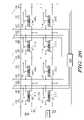
- FIG. 26includes a circuit schematic for an embodiment as described with respect to the embodiment as illustrated in FIG. 27 .
- Memory cells 2111 , 2112 , 2113 , 2114 , 2121 , 2122 , 2123 , and 2124are oriented within the NVM array 18 , as illustrated in FIG. 26 .
- BL 1 2161is electrically connected to S/D regions of the memory cells 2111 , 2112 , 2113 , and 2114
- BL 2 2162is electrically connected to the other S/D region of the memory cells 2111 , 2112 , 2113 , and 2114
- BL 3 2163is electrically connected to S/D regions of the memory cells 2121 , 2122 , 2123 , and 2124
- BL 4 2164is electrically connected to the other S/D region of the memory cells 2121 , 2122 , 2123 , and 2124 .
- SG 1 2101is electrically connected to select gate electrodes of the memory cells 2111 and 2121
- CG 1 2181is electrically connected to control gate electrodes of the memory cells 2111 and 2121
- SG 2 2102is electrically connected to other select gate electrodes of the memory cells 2111 and 2121
- SG 3 2103is electrically connected to select gate electrodes of the memory cells 2112 and 2122
- CG 2 2182is electrically connected to control gate electrodes of the memory cells 2112 and 2122
- SG 4 2104is electrically connected to other select gate electrodes of the memory cells 2112 and 2122 .
- SG 5 2105is electrically connected to select gate electrodes of the memory cells 2113 and 2123
- CG 3 2183is electrically connected to control gate electrodes of the memory cells 2113 and 2123
- SG 6 2106is electrically connected to other select gate electrodes of the memory cells 2113 and 2123
- SG 7 2107is electrically connected to select gate electrodes of the memory cells 2114 and 2124
- CG 4 2184is electrically connected to control gate electrodes of the memory cells 2114 and 2124
- SG 8 2108is electrically connected to other select gate electrodes of the memory cells 2114 and 2124 .
- a bit line control module 2192is coupled to BL 1 2161 , BL 2 2162 , and BL 3 2163 , and BL 4 , 2164 .
- a gate line control module 2194is coupled to SG 1 2101 , CG 1 2181 , SG 2 2102 , SG 2 2102 , CG 2 2182 , SG 3 2103 , SG 4 2104 , CG 3 2183 , SG 6 2106 , SG 7 2107 , CG 4 2184 , and SG 8 2108 .
- Each of the bit line control module 2192 and the gate line control module 2194are conventional or proprietary and may include row or column decoders, voltage drivers, other suitable circuits to operate the NVM array 18 , or any combination thereof.
- Each of the bit line control module 2192 and the gate line control module 2194can include more than one control module.
- Each of the bit line control module 2192 and the gate line control module 2194can the bit lines to be biased or electrically float to achieve the proper operation of the NVM array 18 .
- FIG. 27illustrates a physical embodiment of a portion of the NVM array 18 corresponding to the row that includes the memory cells 2111 , 2112 , 2113 , and 2114 .
- FIG. 27is substantially the same as FIG. 13 except that reference numbers as used in the circuit schematics are used in FIG. 27 .
- the memory cell 2111includes charge storage regions 21111 and 21112
- the memory cell 2112includes charge storage regions 21121 and 21122
- the memory cell 2113includes charge storage regions includes charge storage regions 21131 and 21132
- the memory cell 2114includes charge storage regions 21141 and 21142 .
- the memory cells 2121 to 2124include similar charge storage regions to the memory cells 2111 to 2114 , respectively, but are not illustrated in FIG. 27 .
- FIG. 28includes a table that has some of the operating voltages for memory cells along the top row of memory cells, as illustrated in FIG. 26 .
- BL 1 2161 and BL 2 2162are biased to allow electrons to flow from BL 2 2161 to BL 1 2161 .
- Each of SG 1 2101 , CG 1 2181 , and SG 2 2142is biased to allow carriers to flow through the channel regions of memory cell 2111 .
- All other select gate lines and control gate linese.g., SG 3 2103 , CG 2 2182 , etc.
- BL 3 2163 and BL 4 2164are allowed to electrically float.
- BL 3 2163 and BL 4 2164can be at substantially 0 volts.
- the channel region of the memory cell 2111allows electrons to flow between BL 2 2162 and BL 1 2161 .
- the channel region of the memory cell 2111is adjacent to SG 1 2101 , CG 1 2181 , and SG 2 2102 and between doped regions 114 and 116 .
- SG 1 2101 , CG 1 2181 , and SG 1 2102are biased to allow electrons to flow from the doped region 116 to the doped region 114 .
- the electrical field generated in the channel region of the memory cell 2111 near the doped region 114 (via BL 1 2161 ) and SG 1 2101is sufficient to generate hot carriers within the channel region of memory cell 2111 near doped region 114 . At least some of the hot carriers are attracted to the discontinuous storage elements at the charge storage region 21111 near the junction formed near the doped region 114 within the substrate 12 .
- the charge storage region 21112 within the memory cell 2111is not programmed because SG 1 2101 and SG 2 2102 are at substantially similar voltages, and CG 1 2181 is at a significantly higher voltage.
- Memory cells 2112 , 2113 , 2114 , and 2121 to 2124are not programmed because the voltages on the other select gate lines and control gate lines are zero, and because BL 3 2163 and BL 4 2164 are electrically float or are at substantially the same voltage so that no current flows between those bit lines.
- the voltage difference between CG 1 2181 and BL 2 2162is in a range of approximately one to two times higher than the voltage difference between BL 1 2161 and BL 2 2162 , and the voltage differences between SG 1 2181 and BL 2 2162 and between SG 2 2182 and BL 2 2162 are less than the voltage difference between BL 1 2161 and BL 2 2162 .
- the voltage difference between CG 1 2181 and BL 2 2162is greater than approximately 1.5 times the voltage difference between BL 1 2161 and BL 2 2162 , and the voltage differences between SG 1 2101 and BL 2 2162 and between SG 2 2182 and BL 2 2162 are in a range of approximately 0.4 to 0.8 times the voltage difference between BL 1 2161 and BL 2 2162 .
- Charge storage region 21112can be programmed using the voltages as listed in FIG. 28 . As compared to charge storage region 21111 , the voltages on BL 1 2161 and BL 2 2162 are reversed. The programming mechanism is substantially the same as described with respect to charge storage region 21111 , except that the electrons flow through the channel from the doped region 114 (via BL 1 2161 ) to the doped region 116 (via BL 2 2162 ). The relative comparisons of the voltages described with respect to charge storage region 21111 are the same except that references to BL 2 2162 are replaced by BL 1 2161 , and references to BL 1 2161 are replaced by BL 2 2162 .
- all charge storage regions for all the memory cells within the NVM array 18are programmed using SSI. All other charge storage regions for memory cells 2112 to 2114 and 2121 to 2124 are similar to memory cell 2111 . Each memory cell in FIG. 26 can store up to two bits of data.
- Erasing of NVM array 18can be accomplished by creating a potential difference in a range of about 12 to 16 volts between substrate 12 (or well region therein) and the gate electrodes of the memory cells.
- erasingcan be performed by biasing substrate 12 (or associated well region therein) to approximately ⁇ 7 volts, setting the control gate lines to approximately +7 volts, and allowing the bit lines to electrically float.
- the voltages used for substrate 12 and the control gate linesdo not need to be symmetric with respect to 0 volts. For example, a combination of ⁇ 5 volts and +9 volts can be used. After reading this specification, skilled artisans will be able to determine a set of voltages to be used for erasing that meets their needs or desires.
- the reading of data within NVM array 18 for memory cells 2111 to 2114 and 2121 to 2124is given in FIG. 28 .
- BL 1 2161 and BL 2 2162are biased so that electrons flow from BL 2 2162 to BL 1 2161 .
- SG 1 2101 and CG 1 2181are biased to substantially the same voltage, and SG 2 2102 is biased to a significantly higher voltage.
- the voltage differences between SG 1 2101 and BL 2 2162 and between CG 1 2181 and BL 2 2162are approximately 0.24 to 0.5 times the voltage difference between SG 2 2102 and BL 2 2162 .
- a sense amplifier(not illustrated) coupled to the BL 1 2161 or BL 2 2162 will detect a higher level of current when the charge storage region 21111 is not programmed compared to when the charge storage region 21111 is programmed.
- each memory cellcan include sets of discontinuous storage elements, as described with respect to FIGS. 22 to 25 .
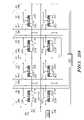
- FIG. 29includes a circuit schematic for that embodiment and is described with respect to the embodiment as illustrated in FIG. 30 .
- Memory cells 2411 , 2412 , 2413 , 2414 , 2421 , 2422 , 2423 , and 2424are oriented within the NVM array 18 , as illustrated in FIG. 29 .
- BL 1 2461is electrically connected to S/D regions of the memory cells 2411 , 2412 , 2413 , and 2414
- BL 2 2462is electrically connected to the other S/D region of the memory cells 2411 , 2412 , 2413 , and 2414
- BL 3 2463is electrically connected to S/D regions of the memory cells 2421 , 2422 , 2423 , and 2424
- BL 4 2464is electrically connected to the other S/D region of the memory cells 2421 , 2422 , 2423 , and 2424 .
- GL 1 2441is electrically connected to gate electrodes of the memory cells 2411 and 2421
- SG 1 2401is electrically connected to select gate electrodes of the memory cells 2411 and 2421
- GL 2 2442is electrically connected to other gate electrodes of the memory cells 2411 and 2421
- GL 3 2443is electrically connected to gate electrodes of the memory cells 2412 and 2422
- SG 2 2402is electrically connected to select gate electrodes of the memory cells 2412 and 2422
- GL 4 2444is electrically connected to other gate electrodes of the memory cells 2412 and 2422 .
- GL 5 2445is electrically connected to gate electrodes of the memory cells 2413 and 2423
- SG 3 2403is electrically connected to select gate electrodes of the memory cells 2413 and 2423
- GL 6 2446is electrically connected to other gate electrodes of the memory cells 2413 and 2423
- GL 7 2447is electrically connected to gate electrodes of the memory cells 2414 and 2424
- SG 4 2404is electrically connected to select gate electrodes of the memory cells 2414 and 2424
- GL 8 2448is electrically connected to other gate electrodes of the memory cells 2414 and 2424 .
- Each of the gate electrodes connected to the gate lines(GL 1 2141 to GL 8 2148 ) can act as a control gate electrode under some biasing conditions and act as a select gate electrode under other biasing conditions.
- a bit line control module 2492is coupled to BL 1 2461 , BL 2 2462 , and BL 3 2463 , and BL 4 , 2464 .
- a gate line control module 2494is coupled to GL 1 2441 , SG 1 2401 , GL 2 2442 , GL 2 2442 , SG 2 2402 , GL 3 2443 , GL 4 2444 , SG 3 2403 , GL 6 2446 , GL 7 2447 , SG 4 2404 , and GL 8 2448 .
- Each of the bit line control module 2492 and the gate line control module 2494are conventional or proprietary and may include row or column decoders, voltage drivers, other suitable circuits to operate the NVM array 18 , or any combination thereof.
- FIG. 30illustrates a physical embodiment of a portion of the NVM array 18 corresponding to the row that includes the memory cells 2411 , 2412 , 2413 , and 2414 .
- the memory cell 2411includes charge storage regions 24111 , 24112 , 24113 , and 24114
- the memory cell 2412includes charge storage regions 24121 24122 , 24123 , and 24124
- the memory cell 2413includes charge storage regions includes charge storage regions 24131 24132 , 24133 , and 24134
- the memory cell 2414includes charge storage regions 24141 24142 , 24143 , and 24144 .
- the memory cells 2421 to 2424include similar charge storage regions to the memory cells 2411 to 2414 , respectively, but are not illustrated in FIG. 30 .
- FIGS. 31 and 32include tables that have some of the operating voltages for memory cells along the top row of memory cells, as illustrated in FIG. 29 .
- BL 1 2461 and BL 2 2462are biased to allow electrons to flow from BL 2 2461 to BL 1 2461 .
- Each of GL 1 2441 , SG 1 2401 , and GL 2 2442is biased to allow carriers to flow through the channel regions of memory cell 2411 .
- All other select gate lines and control gate linese.g., GL 3 2443 , SG 2 2402 , etc.
- BL 3 2463 and BL 4 2464are allowed to electrically float.
- the electrical field generated in the channel region of the memory cell 2411 near the doped region 114 (via BL 1 2461 ) and GL 1 2441is sufficient to generate hot carriers within the channel region of memory cell 2411 near doped region 114 . At least some of the hot carriers are attracted to the discontinuous storage elements at the charge storage region 24111 near the, junction formed near the doped region 114 within the substrate 12 .
- the charge storage region 24112 within the memory cell 2411is not programmed because GL 1 2441 and GL 2 2442 are at substantially similar voltages, and SG 1 2401 is at a significantly higher voltage.
- Memory cells 2412 , 2413 , 2414 , and 2421 to 2424are not programmed because the voltages on the other select gate lines and control gate lines are zero, and because BL 3 2463 and BL 4 2464 are electrically float or are at substantially the same voltage so that no current flows between those bit lines.
- the voltage differences between GL 1 2441 and BL 2 2462 , between SG 1 2401 and BL 2 2462 between SLG 2 2442 and BL 2 2462are in a range of approximately one to two times higher than the voltage difference between BL 1 2461 and BL 2 2462 .
- the voltage difference between GL 1 2441 and BL 2 2462is greater than approximately 1.5 times the voltage difference between BL 1 2461 and BL 2 2462 , and the voltage differences between SG 1 2401 and BL 2 2462 and between GL 2 2442 and BL 2 2462 are less than approximately 1.5 times the voltage difference between BL 1 2461 and BL 2 2462 .
- the programming mechanism for charge storage region 24111is HCI.
- the charge storage region 24111can be programmed using Fowler-Nordheim tunneling. Programming the charge storage region 24111 can be accomplished by creating a potential difference in a range of about 12 to 24 volts between BL 1 2461 and GL 1 2441 . In one embodiment, erasing can be performed by biasing BL 1 2461 to approximately +7 volts, setting the GL 1 2441 to approximately ⁇ 7 volts, and allowing the bit lines to electrically float. Note that the voltages used for BL 1 2461 and GL 1 2441 do not need to be symmetric with respect to 0 volts. For example, a combination of +5 volts and ⁇ 9 volts can be used. After reading this specification, skilled artisans will be able to determine a set of voltages to be used for Fowler-Nordheim tunneling that meets their needs or desires.
- Charge storage region 24112can be programmed using the voltages as listed in FIGS. 31 and 32 . As compared to charge storage region 24111 , the voltage on SG 1 2401 is reduced. The relative comparisons of the voltages described with respect to charge storage region 24111 are the same except that the voltage difference between SG 1 2401 and BL 2 2462 is approximately 0.24 to 0.5 times the voltage difference between GL 1 2441 and BL 2 2462 . In this embodiment, the programming mechanism for charge storage region 24112 is SSI.
- charge storage regions 24113 and 24114are similar to charge storage regions 24112 and 24111 , respectively, except that the voltages on GL 1 2441 and GL 2 2442 are reverses, and the voltages on BL 1 2461 and BL 2 2462 are reversed.
- all charge storage regions for all the memory cells within the NVM array 18are programmed using SSI. All other charge storage regions for memory cells 2412 to 2414 and 2421 to 2424 are similar to memory cell 2411 .
- Each memory cell in FIG. 29can store up to two bits of data.
- the voltages on GL 1 2441 and GL 2 2442are reversed, and the voltages on BL 1 2461 and BL 2 2462 are increased.
- the voltages on BL 1 2461 and BL 2 2462are increased by approximately 1 volt.
- the voltage differences between GL 1 2441 and BL 2 2462 , between SG 1 2401 and BL 2 2462 , and between GL 2 2442 and BL 2 2462are approximately 2 to 6 times the voltage difference between BL 1 2461 and BL 2 2462 .
- the processes and structures describedallow memory cells or portions thereof to be formed with gate electrodes and doped regions adjacent to the gate electrodes that have dimensions smaller than the resolution limits of lithographic processes.
- a set of gate electrodesis formed within and outside of each trench. More specifically, the gate electrodes 52 , 92 , and 94 are in the form of spacers, and the doped regions 116 ( FIG. 13 ) or the doped regions 146 (see FIG. 16 ) are adjacent to the gate electrodes 94 .
- the gate electrodes 52act as control gate electrodes or select gate electrodes
- the gate electrodes 92 and 94act as select gate electrodes or control/select gate electrodes.
- an electronic devicecan include a substrate including a trench having a bottom and a first wall, a first gate electrode within the trench and adjacent to the first wall and overlying the bottom of the trench, a second gate electrode overlying the substrate outside of the trench, a third gate electrode within the trench and adjacent to the first gate electrode and overlying the bottom of the trench, and discontinuous storage elements including a first set of discontinuous storage elements, wherein the first set of the discontinuous storage elements lies adjacent to the first wall of the trench.
- the electronic devicefurther includes a first source/drain region and a second source/drain region, wherein the first source/drain region lies within the substrate below the bottom of the trench and adjacent to the third gate electrode, and the second source/drain region lies within the substrate outside of the trench and adjacent to the second gate electrode.
- the first gate electrode, the second gate electrode, the third gate electrode, the first set of discontinuous storage elements, the first source/drain region, and the second source/drain regionare parts of a first memory cell.
- the electronic devicefurther includes a fourth gate electrode within the trench and adjacent to a second wall of the trench and overlying the bottom of the trench, a fifth gate electrode overlying the substrate outside of the trench, a sixth gate electrode within the trench and adjacent to the fourth gate electrode and overlying the bottom of the trench, and a third source/drain region lying within the substrate outside of the trench and adjacent to the fifth gate electrode.
- the discontinuous storage elementsincludes a second set of discontinuous storage elements, wherein the second set of the discontinuous storage elements lies adjacent to the second wall of the trench, and the fourth gate electrode, the fifth gate electrode, the sixth gate electrode, the second set of discontinuous storage elements, the second source/drain region, and the third source/drain region are parts of a second memory cell.
- each of the first memory cell and the second memory cellis operable to store 2 bits of data.
- the first set of discontinuous storage elementslies between the first gate electrode and the first wall.
- each of the first gate electrode, the second gate electrode, and third gate electrodehas an arc-shaped edge.
- the third gate electrodeincludes a base, and the first set of the discontinuous storage elements also underlies the base of the third gate electrode.
- the discontinuous storage elementsincludes a second set of discontinuous storage elements, the first set of discontinuous storage elements lies between the second gate electrode and the substrate, and the second set of discontinuous storage elements lies between the third gate electrode and the bottom of the trench.
- the first gate electrode, the second gate electrode, the third gate electrode, the first set of discontinuous storage elements, and the second set of discontinuous storage elementsare parts of a memory cell operable to store 4 bits of data.
- a process of forming an electronic devicecan include providing a substrate having a primary surface, forming a patterned sacrificial layer over the primary surface of the substrate, forming a trench extending from the primary surface of the substrate, wherein the trench has a first wall and a bottom, and forming discontinuous storage elements over the primary surface and within the trench.
- the processcan also include forming a first gate electrode within the trench and adjacent to the first wall and overlying the bottom of the trench, wherein a portion of the first gate electrode lies at an elevation higher than the primary surface and adjacent to the patterned sacrificial layer, and removing the patterned sacrificial layer after forming the first gate electrode.
- the processcan further include forming a second gate electrode outside the trench and adjacent to the first gate electrode, wherein forming the second gate electrode is performed after removing the patterned sacrificial layer, and removing a portion of the discontinuous storage elements to form a first set of discontinuous storage elements, wherein the first set of the discontinuous storage elements lies adjacent to the first wall of the trench.
- the processfurther includes forming a third gate electrode within the trench and adjacent to the first gate electrode and overlying the bottom of the trench.
- forming the first gate electrodeincludes forming a first gate material over the substrate outside the trench and adjacent to the first wall and the bottom of the trench, wherein forming the first gate material only partly fills the trench, and anisotropically etching the first gate material to form the first gate electrode.
- forming the second gate electrode and forming the third gate electrodeincludes forming a second gate material over the substrate outside the trench and adjacent to the first wall and the bottom of the trench, wherein forming the second gate material is performed after forming the first gate electrode, and anisotropically etching the second gate material to form the second gate electrode and the third gate electrode.
- the processfurther includes forming a fourth gate electrode within the trench and adjacent to a second wall of the trench and overlying the bottom of the trench, wherein forming the first gate electrode and forming the fourth gate electrode are performed substantially simultaneously.
- the processstill further includes forming a fifth gate electrode outside the trench and adjacent to the fourth gate electrode, forming a sixth gate electrode within the trench and adjacent to the fourth gate electrode and overlying the bottom of the trench, wherein forming the second gate electrode, forming the third gate electrode, forming the fifth gate electrode, and forming the sixth gate electrode are performed substantially simultaneously.
- the processyet further includes forming a first source/drain region, a second source/drain region, and a third source drain region.
- the first source/drain regionlies outside the trench and adjacent to the second gate electrode
- the second source/drain regionlies within the substrate beneath the bottom of the trench and adjacent to the third gate electrode and the sixth gate electrode
- the third source/drain regionlies outside the trench and adjacent to the fifth gate electrode
- forming the discontinuous storage elementsis performed before forming the first gate electrode, and removing the portion of the discontinuous storage elements is performed after forming the first gate electrode and before forming the second gate electrode.
- forming the discontinuous storage elementsis performed after forming the first gate electrode and before forming the second gate electrode, and removing the portion of the discontinuous storage elements is performed after forming the second gate electrode, wherein removing the portion also forms a second set of discontinuous storage elements, wherein the first set of discontinuous storage elements lies between the second gate electrode and the substrate.
- a process of using an electronic devicecan include providing a memory cell.
- the memory cellcan include a substrate including a trench having a bottom and a first wall, a first gate electrode within the trench and adjacent to the first wall and overlying the bottom of the trench, a second gate electrode overlying the substrate outside of the trench, and a third gate electrode within the trench and adjacent to the first gate electrode and overlying the bottom of the trench.
- the memory cellcan further include a first source/drain region adjacent to the third gate electrode and coupled to a first bit line, a second source/drain region adjacent to the second gate electrode and coupled to a second bit line, and discontinuous storage elements including a first set of discontinuous storage elements, wherein the first set of the discontinuous storage elements lies adjacent to the first wall of the trench.
- the processcan also include programming a first bit of the memory cell including biasing the first bit line and the second bit line at a first voltage difference, biasing the third gate electrode, such that a second voltage difference between the third gate electrode and the first bit line is no greater than approximately half of the first voltage difference, biasing the first gate electrode, such that a third voltage difference between the first gate electrode and the first bit line is in a range of approximately 0.5 to approximately 1.5 times the first voltage difference, and biasing the second gate electrode, such that a fourth voltage difference between the second gate electrode and the first bit line is in a range of approximately 0.5 to approximately 1.5 times the first voltage difference.
- the processfurther includes programming a second bit of the memory cell including biasing the first bit line and the second bit line at a fifth voltage difference, biasing the second gate electrode, such that a sixth voltage difference between the second gate electrode and the second bit line is no greater than approximately half of the fifth voltage difference, biasing the first gate electrode, such that a seventh voltage difference between the first gate electrode and the second bit line is in a range of approximately 0.5 to approximately 1.5 times the fifth voltage difference, and biasing the third gate electrode, such that an eighth voltage difference between the third gate electrode and the second bit line is in a range of approximately 0.5 to approximately 1.5 times the fifth voltage difference.
- the processfurther includes erasing the memory cell including biasing the substrate and the first gate electrode at a fourth voltage difference, such that the fourth voltage difference has an opposite polarity compared to first voltage difference, and the fourth voltage difference has a magnitude that is at least approximately 4 times a magnitude of the first voltage difference, and electrically floating the first bit line and the second bit line.
Landscapes
- Engineering & Computer Science (AREA)
- Chemical & Material Sciences (AREA)
- Nanotechnology (AREA)
- Physics & Mathematics (AREA)
- Mathematical Physics (AREA)
- Theoretical Computer Science (AREA)
- Crystallography & Structural Chemistry (AREA)
- Semiconductor Memories (AREA)
Abstract
Description
Claims (20)
Priority Applications (1)
| Application Number | Priority Date | Filing Date | Title |
|---|---|---|---|
| US11/626,753US7838922B2 (en) | 2007-01-24 | 2007-01-24 | Electronic device including trenches and discontinuous storage elements |
Applications Claiming Priority (1)
| Application Number | Priority Date | Filing Date | Title |
|---|---|---|---|
| US11/626,753US7838922B2 (en) | 2007-01-24 | 2007-01-24 | Electronic device including trenches and discontinuous storage elements |
Publications (2)
| Publication Number | Publication Date |
|---|---|
| US20080173921A1 US20080173921A1 (en) | 2008-07-24 |
| US7838922B2true US7838922B2 (en) | 2010-11-23 |
Family
ID=39640389
Family Applications (1)
| Application Number | Title | Priority Date | Filing Date |
|---|---|---|---|
| US11/626,753Expired - Fee RelatedUS7838922B2 (en) | 2007-01-24 | 2007-01-24 | Electronic device including trenches and discontinuous storage elements |
Country Status (1)
| Country | Link |
|---|---|
| US (1) | US7838922B2 (en) |
Cited By (6)
| Publication number | Priority date | Publication date | Assignee | Title |
|---|---|---|---|---|
| US20100006914A1 (en)* | 2008-07-14 | 2010-01-14 | Nec Electronics Corporation | Nonvolatile semiconductor memory device, and method for manufacturing nonvolatile semiconductor memory device |
| US8193572B2 (en) | 2007-01-24 | 2012-06-05 | Freescale Semiconductor, Inc. | Electronic device including trenches and discontinuous storage elements |
| US20130187215A1 (en)* | 2006-08-09 | 2013-07-25 | Micron Technology, Inc. | Methods of forming nanoscale floating gate |
| US9257445B2 (en)* | 2014-05-30 | 2016-02-09 | Freescale Semiconductor, Inc. | Method of making a split gate non-volatile memory (NVM) cell and a logic transistor |
| US20160056250A1 (en)* | 2014-08-25 | 2016-02-25 | Taiwan Semiconductor Manufacturing Co., Ltd. | Recessed Salicide Structure to Integrate a Flash Memory Device with a High K, Metal Gate Logic Device |
| US12170340B1 (en)* | 2023-07-03 | 2024-12-17 | Diodes Incorporated | Semiconductor rectifier and manufacturing method of the same |
Families Citing this family (12)
| Publication number | Priority date | Publication date | Assignee | Title |
|---|---|---|---|---|
| US7592224B2 (en) | 2006-03-30 | 2009-09-22 | Freescale Semiconductor, Inc | Method of fabricating a storage device including decontinuous storage elements within and between trenches |
| US8836005B2 (en)* | 2008-10-31 | 2014-09-16 | Macronix International Co., Ltd. | Memory array |
| US9263132B2 (en)* | 2011-08-10 | 2016-02-16 | Globalfoundries Singapore Pte. Ltd. | Double gated flash memory |
| US8951892B2 (en) | 2012-06-29 | 2015-02-10 | Freescale Semiconductor, Inc. | Applications for nanopillar structures |
| US8853027B2 (en) | 2012-10-01 | 2014-10-07 | Freescale Semiconductor, Inc. | Split gate flash cell |
| US10312247B1 (en)* | 2018-03-22 | 2019-06-04 | Silicon Storage Technology, Inc. | Two transistor FinFET-based split gate non-volatile floating gate flash memory and method of fabrication |
| US10468428B1 (en) | 2018-04-19 | 2019-11-05 | Silicon Storage Technology, Inc. | Split gate non-volatile memory cells and logic devices with FinFET structure, and method of making same |
| US10727240B2 (en) | 2018-07-05 | 2020-07-28 | Silicon Store Technology, Inc. | Split gate non-volatile memory cells with three-dimensional FinFET structure |
| US10797142B2 (en) | 2018-12-03 | 2020-10-06 | Silicon Storage Technology, Inc. | FinFET-based split gate non-volatile flash memory with extended source line FinFET, and method of fabrication |
| US10937794B2 (en) | 2018-12-03 | 2021-03-02 | Silicon Storage Technology, Inc. | Split gate non-volatile memory cells with FinFET structure and HKMG memory and logic gates, and method of making same |
| US11362100B2 (en) | 2020-03-24 | 2022-06-14 | Silicon Storage Technology, Inc. | FinFET split gate non-volatile memory cells with enhanced floating gate to floating gate capacitive coupling |
| KR102773451B1 (en)* | 2021-08-06 | 2025-02-27 | 창신 메모리 테크놀로지즈 아이엔씨 | Semiconductor structure and method for manufacturing semiconductor structure |
Citations (101)
| Publication number | Priority date | Publication date | Assignee | Title |
|---|---|---|---|---|
| US4184207A (en) | 1978-01-27 | 1980-01-15 | Texas Instruments Incorporated | High density floating gate electrically programmable ROM |
| US4751558A (en) | 1985-10-31 | 1988-06-14 | International Business Machines Corporation | High density memory with field shield |
| US4785337A (en) | 1986-10-17 | 1988-11-15 | International Business Machines Corporation | Dynamic ram cell having shared trench storage capacitor with sidewall-defined bridge contacts and gate electrodes |
| US4833094A (en) | 1986-10-17 | 1989-05-23 | International Business Machines Corporation | Method of making a dynamic ram cell having shared trench storage capacitor with sidewall-defined bridge contacts and gate electrodes |
| US4860070A (en) | 1987-01-09 | 1989-08-22 | Mitsubishi Denki Kabushiki Kaisha | Semiconductor memory device comprising trench memory cells |
| US5196722A (en) | 1992-03-12 | 1993-03-23 | International Business Machines Corporation | Shadow ram cell having a shallow trench eeprom |
| US5252845A (en) | 1990-04-02 | 1993-10-12 | Electronics And Telecommunications Research Institute | Trench DRAM cell with vertical transistor |
| US5315142A (en) | 1992-03-23 | 1994-05-24 | International Business Machines Corporation | High performance trench EEPROM cell |
| US5411905A (en) | 1994-04-29 | 1995-05-02 | International Business Machines Corporation | Method of making trench EEPROM structure on SOI with dual channels |
| US5432365A (en) | 1988-02-15 | 1995-07-11 | Samsung Electronics Co., Ltd. | Semiconductor memory device |
| US5460988A (en) | 1994-04-25 | 1995-10-24 | United Microelectronics Corporation | Process for high density flash EPROM cell |
| US5705415A (en) | 1994-10-04 | 1998-01-06 | Motorola, Inc. | Process for forming an electrically programmable read-only memory cell |
| US5721448A (en) | 1996-07-30 | 1998-02-24 | International Business Machines Corporation | Integrated circuit chip having isolation trenches composed of a dielectric layer with oxidation catalyst material |
| US5786612A (en) | 1995-10-25 | 1998-07-28 | Mitsubishi Denki Kabushiki Kaisha | Semiconductor device comprising trench EEPROM |
| US5801415A (en) | 1996-05-16 | 1998-09-01 | Taiwan Semiconductor Manufacturing Company Ltd. | Non-volatile-memory cell for electrically programmable read only memory having a trench-like coupling capacitors |
| US5824580A (en) | 1996-07-30 | 1998-10-20 | International Business Machines Corporation | Method of manufacturing an insulated gate field effect transistor |
| US5907775A (en) | 1997-04-11 | 1999-05-25 | Vanguard International Semiconductor Corporation | Non-volatile memory device with high gate coupling ratio and manufacturing process therefor |
| US5914523A (en) | 1998-02-17 | 1999-06-22 | National Semiconductor Corp. | Semiconductor device trench isolation structure with polysilicon bias voltage contact |
| US5923046A (en) | 1996-09-13 | 1999-07-13 | Kabushiki Kaisha Toshiba | Quantum dot memory cell |
| US5969383A (en) | 1997-06-16 | 1999-10-19 | Motorola, Inc. | Split-gate memory device and method for accessing the same |
| US5998263A (en) | 1996-05-16 | 1999-12-07 | Altera Corporation | High-density nonvolatile memory cell |
| US6060743A (en) | 1997-05-21 | 2000-05-09 | Kabushiki Kaisha Toshiba | Semiconductor memory device having multilayer group IV nanocrystal quantum dot floating gate and method of manufacturing the same |
| US6074954A (en) | 1998-08-31 | 2000-06-13 | Applied Materials, Inc | Process for control of the shape of the etch front in the etching of polysilicon |
| US6117733A (en) | 1998-05-27 | 2000-09-12 | Taiwan Semiconductor Manufacturing Company | Poly tip formation and self-align source process for split-gate flash cell |
| US6133601A (en) | 1996-12-11 | 2000-10-17 | Kabushiki Kaisha Toshiba | Non-volatile semiconductor memory device with inter-layer insulation film |
| US6172905B1 (en) | 2000-02-01 | 2001-01-09 | Motorola, Inc. | Method of operating a semiconductor device |
| US6228706B1 (en) | 1999-08-26 | 2001-05-08 | International Business Machines Corporation | Vertical DRAM cell with TFT over trench capacitor |
| US6232632B1 (en) | 1998-07-07 | 2001-05-15 | Advanced Micro Devices, Inc. | Double density non-volatile memory cells |
| US6265268B1 (en) | 1999-10-25 | 2001-07-24 | Advanced Micro Devices, Inc. | High temperature oxide deposition process for fabricating an ONO floating-gate electrode in a two bit EEPROM device |
| US6281064B1 (en) | 1999-06-04 | 2001-08-28 | International Business Machines Corporation | Method for providing dual work function doping and protective insulating cap |
| US6287917B1 (en) | 1999-09-08 | 2001-09-11 | Advanced Micro Devices, Inc. | Process for fabricating an MNOS flash memory device |
| US6307782B1 (en) | 2000-04-03 | 2001-10-23 | Motorola, Inc. | Process for operating a semiconductor device |
| US6320784B1 (en) | 2000-03-14 | 2001-11-20 | Motorola, Inc. | Memory cell and method for programming thereof |
| US6344403B1 (en) | 2000-06-16 | 2002-02-05 | Motorola, Inc. | Memory device and method for manufacture |
| US6365452B1 (en) | 1998-03-19 | 2002-04-02 | Lsi Logic Corporation | DRAM cell having a vertical transistor and a capacitor formed on the sidewalls of a trench isolation |
| US6368916B1 (en) | 1999-10-22 | 2002-04-09 | Fujitsu Limited | Method for fabricating nonvolatile semiconductor memory device |
| US6372617B1 (en) | 1997-12-17 | 2002-04-16 | Nec Corporation | Method of manufacturing non-volatile memory |
| US6373096B1 (en) | 1999-01-22 | 2002-04-16 | Nec Corporation | Method of manufacturing semiconductor device, nonvolatile semiconductor memory device and method of manufacturing the same |
| US6399441B1 (en) | 1999-08-05 | 2002-06-04 | Halo Lsi Device & Design Technology, Inc. | Nonvolatile memory cell, method of programming the same and nonvolatile memory array |
| US6433382B1 (en)* | 1995-04-06 | 2002-08-13 | Motorola, Inc. | Split-gate vertically oriented EEPROM device and process |
| US6461905B1 (en) | 2002-02-22 | 2002-10-08 | Advanced Micro Devices, Inc. | Dummy gate process to reduce the Vss resistance of flash products |
| US6486028B1 (en) | 2001-11-20 | 2002-11-26 | Macronix International Co., Ltd. | Method of fabricating a nitride read-only-memory cell vertical structure |
| US6537870B1 (en) | 2000-09-29 | 2003-03-25 | Infineon Technologies Ag | Method of forming an integrated circuit comprising a self aligned trench |
| US20030062565A1 (en) | 1996-01-22 | 2003-04-03 | Semiconductor Energy Laboratory Co., Ltd., A Japanese Corporation | Semiconductor device and method of fabricating same |
| US6544827B2 (en) | 1998-08-24 | 2003-04-08 | Nec Corporation | Metal-gate field effect transistor and method for manufacturing the same |
| US20030068864A1 (en) | 2001-10-10 | 2003-04-10 | Park Il-Yong | Method for fabricating power semiconductor device having trench gate structure |
| US20030071302A1 (en) | 1997-04-25 | 2003-04-17 | Nippon Steel Corporation | Multi-level type nonvolatile semiconductor memory device |
| US6555427B1 (en) | 1999-08-31 | 2003-04-29 | Kabushiki Kaisha Toshiba | Non-volatile semiconductor memory device and manufacturing method thereof |
| US6559032B2 (en) | 1996-01-05 | 2003-05-06 | Micron Technology, Inc. | Method of fabricating an isolation structure on a semiconductor substrate |
| US6583466B2 (en) | 1998-03-05 | 2003-06-24 | Taiwan Semiconductor Manufacturing Company | Vertical split gate flash memory device in an orthogonal array of rows and columns with devices in columns having shared source regions |
| US6620664B2 (en) | 2002-02-07 | 2003-09-16 | Sharp Laboratories Of America, Inc. | Silicon-germanium MOSFET with deposited gate dielectric and metal gate electrode and method for making the same |
| US6638810B2 (en) | 2000-02-22 | 2003-10-28 | Applied Materials, Inc. | Tantalum nitride CVD deposition by tantalum oxide densification |
| US6674120B2 (en) | 2000-05-02 | 2004-01-06 | Sony Corporation | Nonvolatile semiconductor memory device and method of operation thereof |
| US6673681B2 (en) | 1999-05-19 | 2004-01-06 | Fairchild Semiconductor Corporation | Process for forming MOS-gated power device having segmented trench and extended doping zone |
| US6677204B2 (en) | 2000-08-14 | 2004-01-13 | Matrix Semiconductor, Inc. | Multigate semiconductor device with vertical channel current and method of fabrication |
| US6687156B2 (en) | 1999-07-14 | 2004-02-03 | Hitachi, Ltd. | Semiconductor integrated circuit device, production and operation method thereof |
| US6706599B1 (en) | 2003-03-20 | 2004-03-16 | Motorola, Inc. | Multi-bit non-volatile memory device and method therefor |
| US6709922B2 (en) | 2001-01-30 | 2004-03-23 | Seiko Epson Corporation | Method of manufacturing semiconductor integrated circuit device including nonvolatile semiconductor memory devices |
| US6713834B2 (en) | 2000-10-30 | 2004-03-30 | Kabushiki Kaisha Toshiba | Semiconductor device having two-layered charge storage electrode |
| US6747308B2 (en) | 2001-12-28 | 2004-06-08 | Texas Instruments Incorporated | Single poly EEPROM with reduced area |
| US6750499B2 (en) | 2002-08-06 | 2004-06-15 | Intelligent Sources Development Corp. | Self-aligned trench-type dram structure and its contactless dram arrays |
| US20040121540A1 (en) | 2002-12-17 | 2004-06-24 | Chi-Hui Lin | Stacked gate flash memory device and method of fabricating the same |
| US6762092B2 (en) | 2001-08-08 | 2004-07-13 | Sandisk Corporation | Scalable self-aligned dual floating gate memory cell array and methods of forming the array |
| US6803620B2 (en) | 2000-10-27 | 2004-10-12 | Sony Corporation | Non-volatile semiconductor memory device and a method of producing the same |
| US6816414B1 (en) | 2003-07-31 | 2004-11-09 | Freescale Semiconductor, Inc. | Nonvolatile memory and method of making same |
| US6818939B1 (en) | 2003-07-18 | 2004-11-16 | Semiconductor Components Industries, L.L.C. | Vertical compound semiconductor field effect transistor structure |
| US6818512B1 (en) | 2002-01-04 | 2004-11-16 | Taiwan Semiconductor Manufacturing Company | Split-gate flash with source/drain multi-sharing |
| US6853587B2 (en) | 2002-06-21 | 2005-02-08 | Micron Technology, Inc. | Vertical NROM having a storage density of 1 bit per 1F2 |
| US6861315B1 (en) | 2003-08-14 | 2005-03-01 | Silicon Storage Technology, Inc. | Method of manufacturing an array of bi-directional nonvolatile memory cells |
| US6864540B1 (en) | 2004-05-21 | 2005-03-08 | International Business Machines Corp. | High performance FET with elevated source/drain region |
| US6881994B2 (en) | 2000-08-14 | 2005-04-19 | Matrix Semiconductor, Inc. | Monolithic three dimensional array of charge storage devices containing a planarized surface |
| US6894339B2 (en) | 2003-01-02 | 2005-05-17 | Actrans System Inc. | Flash memory with trench select gate and fabrication process |
| US6903418B2 (en) | 2001-02-09 | 2005-06-07 | Fuji Electric Device Technology Co., Ltd. | Semiconductor device |
| US20050148173A1 (en) | 2004-01-05 | 2005-07-07 | Fuja Shone | Non-volatile memory array having vertical transistors and manufacturing method thereof |
| US20050146938A1 (en) | 1997-01-29 | 2005-07-07 | Micron Technology, Inc. | Transistor with nanocrystalline silicon gate structure |
| US6916715B2 (en) | 2002-11-18 | 2005-07-12 | Nanya Technology Corporation | Method for fabricating a vertical NROM cell |
| US6936887B2 (en) | 2001-05-18 | 2005-08-30 | Sandisk Corporation | Non-volatile memory cells utilizing substrate trenches |
| US6952034B2 (en) | 2002-04-05 | 2005-10-04 | Silicon Storage Technology, Inc. | Semiconductor memory array of floating gate memory cells with buried source line and floating gate |
| US6958513B2 (en) | 2003-06-06 | 2005-10-25 | Chih-Hsin Wang | Floating-gate memory cell having trench structure with ballistic-charge injector, and the array of memory cells |
| US20050242391A1 (en) | 2004-05-03 | 2005-11-03 | The Regents Of The University Of California | Two bit/four bit SONOS flash memory cell |
| US20050259475A1 (en) | 2004-05-18 | 2005-11-24 | Micron Technology, Inc. | Ballistic injection nrom flash memory |
| US20050280089A1 (en) | 2003-11-17 | 2005-12-22 | Micron Technology, Inc. | NROM flash memory devices on ultrathin silicon |
| US20050285177A1 (en)* | 2004-06-29 | 2005-12-29 | Skymedi Corporation | Vertical memory cell and manufacturing method thereof |
| US20060011966A1 (en) | 2004-07-15 | 2006-01-19 | Promos Technologies Inc. | Structure of a non-volatile memory cell and method of forming the same |
| US6991984B2 (en) | 2004-01-27 | 2006-01-31 | Freescale Semiconductor, Inc. | Method for forming a memory structure using a modified surface topography and structure thereof |
| US20060046383A1 (en) | 2004-09-02 | 2006-03-02 | Shenlin Chen | Method for forming a nanocrystal floating gate for a flash memory device |
| US7015537B2 (en) | 2004-04-12 | 2006-03-21 | Silicon Storage Technology, Inc. | Isolation-less, contact-less array of nonvolatile memory cells each having a floating gate for storage of charges, and methods of manufacturing, and operating therefor |
| US7045423B2 (en) | 2001-05-28 | 2006-05-16 | Kabushiki Kaisha Toshiba | Non-volatile semiconductor memory device with multi-layer gate structure |
| US20060131640A1 (en) | 2004-03-16 | 2006-06-22 | Andy Yu | Memory array of non-volatile electrically alterable memory cells for storing multiple data |
| US20060152978A1 (en) | 2003-12-16 | 2006-07-13 | Micron Technology, Inc. | Multi-state NROM device |
| US7078286B1 (en) | 2002-09-06 | 2006-07-18 | Lattice Semiconductor Corporation | Process for fabricating a semiconductor device having electrically isolated low voltage and high voltage regions |
| US7098502B2 (en) | 2003-11-10 | 2006-08-29 | Freescale Semiconductor, Inc. | Transistor having three electrically isolated electrodes and method of formation |
| US7112490B1 (en) | 2005-07-25 | 2006-09-26 | Freescale Semiconductor, Inc. | Hot carrier injection programmable structure including discontinuous storage elements and spacer control gates in a trench |
| US7126188B2 (en) | 2004-05-27 | 2006-10-24 | Skymedi Corporation | Vertical split gate memory cell and manufacturing method thereof |
| US20070019472A1 (en)* | 2005-07-25 | 2007-01-25 | Freescale Semiconductor, Inc. | Electronic device including a memory array and conductive lines |
| US7192830B2 (en) | 2003-06-13 | 2007-03-20 | Infineon Technologies Ag | Method for fabricating a memory cell |
| US7199419B2 (en) | 2004-12-13 | 2007-04-03 | Micron Technology, Inc. | Memory structure for reduced floating body effect |
| US7220634B2 (en) | 2002-06-21 | 2007-05-22 | Micron Technology, Inc. | NROM memory cell, memory array, related devices and methods |
| US7259984B2 (en) | 2002-11-26 | 2007-08-21 | Cornell Research Foundation, Inc. | Multibit metal nanocrystal memories and fabrication |
| US7279740B2 (en) | 2005-05-12 | 2007-10-09 | Micron Technology, Inc. | Band-engineered multi-gated non-volatile memory device with enhanced attributes |
| US20070238249A1 (en) | 2006-03-30 | 2007-10-11 | Freescale Semiconductor, Inc. | Programmable structure including control gate overlying select gate formed in a trench |
- 2007
- 2007-01-24USUS11/626,753patent/US7838922B2/ennot_activeExpired - Fee Related
Patent Citations (110)
| Publication number | Priority date | Publication date | Assignee | Title |
|---|---|---|---|---|
| US4184207A (en) | 1978-01-27 | 1980-01-15 | Texas Instruments Incorporated | High density floating gate electrically programmable ROM |
| US4751558A (en) | 1985-10-31 | 1988-06-14 | International Business Machines Corporation | High density memory with field shield |
| US4785337A (en) | 1986-10-17 | 1988-11-15 | International Business Machines Corporation | Dynamic ram cell having shared trench storage capacitor with sidewall-defined bridge contacts and gate electrodes |
| US4833094A (en) | 1986-10-17 | 1989-05-23 | International Business Machines Corporation | Method of making a dynamic ram cell having shared trench storage capacitor with sidewall-defined bridge contacts and gate electrodes |
| US4860070A (en) | 1987-01-09 | 1989-08-22 | Mitsubishi Denki Kabushiki Kaisha | Semiconductor memory device comprising trench memory cells |
| US5432365A (en) | 1988-02-15 | 1995-07-11 | Samsung Electronics Co., Ltd. | Semiconductor memory device |
| US5252845A (en) | 1990-04-02 | 1993-10-12 | Electronics And Telecommunications Research Institute | Trench DRAM cell with vertical transistor |
| US5196722A (en) | 1992-03-12 | 1993-03-23 | International Business Machines Corporation | Shadow ram cell having a shallow trench eeprom |
| US5315142A (en) | 1992-03-23 | 1994-05-24 | International Business Machines Corporation | High performance trench EEPROM cell |
| US5567635A (en) | 1992-03-23 | 1996-10-22 | International Business Machines Corporation | Method of making a three dimensional trench EEPROM cell structure |
| US5460988A (en) | 1994-04-25 | 1995-10-24 | United Microelectronics Corporation | Process for high density flash EPROM cell |
| US5411905A (en) | 1994-04-29 | 1995-05-02 | International Business Machines Corporation | Method of making trench EEPROM structure on SOI with dual channels |
| US5705415A (en) | 1994-10-04 | 1998-01-06 | Motorola, Inc. | Process for forming an electrically programmable read-only memory cell |
| US6433382B1 (en)* | 1995-04-06 | 2002-08-13 | Motorola, Inc. | Split-gate vertically oriented EEPROM device and process |
| US5786612A (en) | 1995-10-25 | 1998-07-28 | Mitsubishi Denki Kabushiki Kaisha | Semiconductor device comprising trench EEPROM |
| US6559032B2 (en) | 1996-01-05 | 2003-05-06 | Micron Technology, Inc. | Method of fabricating an isolation structure on a semiconductor substrate |
| US20030062565A1 (en) | 1996-01-22 | 2003-04-03 | Semiconductor Energy Laboratory Co., Ltd., A Japanese Corporation | Semiconductor device and method of fabricating same |
| US5998263A (en) | 1996-05-16 | 1999-12-07 | Altera Corporation | High-density nonvolatile memory cell |
| US5801415A (en) | 1996-05-16 | 1998-09-01 | Taiwan Semiconductor Manufacturing Company Ltd. | Non-volatile-memory cell for electrically programmable read only memory having a trench-like coupling capacitors |
| US5824580A (en) | 1996-07-30 | 1998-10-20 | International Business Machines Corporation | Method of manufacturing an insulated gate field effect transistor |
| US5721448A (en) | 1996-07-30 | 1998-02-24 | International Business Machines Corporation | Integrated circuit chip having isolation trenches composed of a dielectric layer with oxidation catalyst material |
| US5923046A (en) | 1996-09-13 | 1999-07-13 | Kabushiki Kaisha Toshiba | Quantum dot memory cell |
| US6133601A (en) | 1996-12-11 | 2000-10-17 | Kabushiki Kaisha Toshiba | Non-volatile semiconductor memory device with inter-layer insulation film |
| US20050146938A1 (en) | 1997-01-29 | 2005-07-07 | Micron Technology, Inc. | Transistor with nanocrystalline silicon gate structure |
| US5907775A (en) | 1997-04-11 | 1999-05-25 | Vanguard International Semiconductor Corporation | Non-volatile memory device with high gate coupling ratio and manufacturing process therefor |
| US20030071302A1 (en) | 1997-04-25 | 2003-04-17 | Nippon Steel Corporation | Multi-level type nonvolatile semiconductor memory device |
| US6060743A (en) | 1997-05-21 | 2000-05-09 | Kabushiki Kaisha Toshiba | Semiconductor memory device having multilayer group IV nanocrystal quantum dot floating gate and method of manufacturing the same |
| US5969383A (en) | 1997-06-16 | 1999-10-19 | Motorola, Inc. | Split-gate memory device and method for accessing the same |
| US6372617B1 (en) | 1997-12-17 | 2002-04-16 | Nec Corporation | Method of manufacturing non-volatile memory |
| US6121148A (en) | 1998-02-17 | 2000-09-19 | National Semiconductor Corporation | Semiconductor device trench isolation structure with polysilicon bias voltage contact |
| US5914523A (en) | 1998-02-17 | 1999-06-22 | National Semiconductor Corp. | Semiconductor device trench isolation structure with polysilicon bias voltage contact |
| US6583466B2 (en) | 1998-03-05 | 2003-06-24 | Taiwan Semiconductor Manufacturing Company | Vertical split gate flash memory device in an orthogonal array of rows and columns with devices in columns having shared source regions |
| US6365452B1 (en) | 1998-03-19 | 2002-04-02 | Lsi Logic Corporation | DRAM cell having a vertical transistor and a capacitor formed on the sidewalls of a trench isolation |
| US6117733A (en) | 1998-05-27 | 2000-09-12 | Taiwan Semiconductor Manufacturing Company | Poly tip formation and self-align source process for split-gate flash cell |
| US6232632B1 (en) | 1998-07-07 | 2001-05-15 | Advanced Micro Devices, Inc. | Double density non-volatile memory cells |
| US6544827B2 (en) | 1998-08-24 | 2003-04-08 | Nec Corporation | Metal-gate field effect transistor and method for manufacturing the same |
| US6074954A (en) | 1998-08-31 | 2000-06-13 | Applied Materials, Inc | Process for control of the shape of the etch front in the etching of polysilicon |
| US6373096B1 (en) | 1999-01-22 | 2002-04-16 | Nec Corporation | Method of manufacturing semiconductor device, nonvolatile semiconductor memory device and method of manufacturing the same |
| US6673681B2 (en) | 1999-05-19 | 2004-01-06 | Fairchild Semiconductor Corporation | Process for forming MOS-gated power device having segmented trench and extended doping zone |
| US6281064B1 (en) | 1999-06-04 | 2001-08-28 | International Business Machines Corporation | Method for providing dual work function doping and protective insulating cap |
| US6687156B2 (en) | 1999-07-14 | 2004-02-03 | Hitachi, Ltd. | Semiconductor integrated circuit device, production and operation method thereof |
| US6399441B1 (en) | 1999-08-05 | 2002-06-04 | Halo Lsi Device & Design Technology, Inc. | Nonvolatile memory cell, method of programming the same and nonvolatile memory array |
| US6228706B1 (en) | 1999-08-26 | 2001-05-08 | International Business Machines Corporation | Vertical DRAM cell with TFT over trench capacitor |
| US6818508B2 (en) | 1999-08-31 | 2004-11-16 | Kabushiki Kaisha Toshiba | Non-volatile semiconductor memory device and manufacturing method thereof |
| US7122432B2 (en) | 1999-08-31 | 2006-10-17 | Kabushiki Kaisha Toshiba | Non-volatile semiconductor memory device and manufacturing method thereof |
| US6555427B1 (en) | 1999-08-31 | 2003-04-29 | Kabushiki Kaisha Toshiba | Non-volatile semiconductor memory device and manufacturing method thereof |
| US6287917B1 (en) | 1999-09-08 | 2001-09-11 | Advanced Micro Devices, Inc. | Process for fabricating an MNOS flash memory device |
| US6368916B1 (en) | 1999-10-22 | 2002-04-09 | Fujitsu Limited | Method for fabricating nonvolatile semiconductor memory device |
| US6265268B1 (en) | 1999-10-25 | 2001-07-24 | Advanced Micro Devices, Inc. | High temperature oxide deposition process for fabricating an ONO floating-gate electrode in a two bit EEPROM device |
| US6172905B1 (en) | 2000-02-01 | 2001-01-09 | Motorola, Inc. | Method of operating a semiconductor device |
| US6330184B1 (en) | 2000-02-01 | 2001-12-11 | Motorola, Inc. | Method of operating a semiconductor device |
| US6638810B2 (en) | 2000-02-22 | 2003-10-28 | Applied Materials, Inc. | Tantalum nitride CVD deposition by tantalum oxide densification |
| US6320784B1 (en) | 2000-03-14 | 2001-11-20 | Motorola, Inc. | Memory cell and method for programming thereof |
| US6307782B1 (en) | 2000-04-03 | 2001-10-23 | Motorola, Inc. | Process for operating a semiconductor device |
| US6674120B2 (en) | 2000-05-02 | 2004-01-06 | Sony Corporation | Nonvolatile semiconductor memory device and method of operation thereof |
| US6344403B1 (en) | 2000-06-16 | 2002-02-05 | Motorola, Inc. | Memory device and method for manufacture |
| US6881994B2 (en) | 2000-08-14 | 2005-04-19 | Matrix Semiconductor, Inc. | Monolithic three dimensional array of charge storage devices containing a planarized surface |
| US6677204B2 (en) | 2000-08-14 | 2004-01-13 | Matrix Semiconductor, Inc. | Multigate semiconductor device with vertical channel current and method of fabrication |
| US6537870B1 (en) | 2000-09-29 | 2003-03-25 | Infineon Technologies Ag | Method of forming an integrated circuit comprising a self aligned trench |
| US6803620B2 (en) | 2000-10-27 | 2004-10-12 | Sony Corporation | Non-volatile semiconductor memory device and a method of producing the same |
| US6713834B2 (en) | 2000-10-30 | 2004-03-30 | Kabushiki Kaisha Toshiba | Semiconductor device having two-layered charge storage electrode |
| US6709922B2 (en) | 2001-01-30 | 2004-03-23 | Seiko Epson Corporation | Method of manufacturing semiconductor integrated circuit device including nonvolatile semiconductor memory devices |
| US6903418B2 (en) | 2001-02-09 | 2005-06-07 | Fuji Electric Device Technology Co., Ltd. | Semiconductor device |
| US6936887B2 (en) | 2001-05-18 | 2005-08-30 | Sandisk Corporation | Non-volatile memory cells utilizing substrate trenches |
| US7045423B2 (en) | 2001-05-28 | 2006-05-16 | Kabushiki Kaisha Toshiba | Non-volatile semiconductor memory device with multi-layer gate structure |
| US6762092B2 (en) | 2001-08-08 | 2004-07-13 | Sandisk Corporation | Scalable self-aligned dual floating gate memory cell array and methods of forming the array |
| US20030068864A1 (en) | 2001-10-10 | 2003-04-10 | Park Il-Yong | Method for fabricating power semiconductor device having trench gate structure |
| US6486028B1 (en) | 2001-11-20 | 2002-11-26 | Macronix International Co., Ltd. | Method of fabricating a nitride read-only-memory cell vertical structure |
| US6747308B2 (en) | 2001-12-28 | 2004-06-08 | Texas Instruments Incorporated | Single poly EEPROM with reduced area |
| US6818512B1 (en) | 2002-01-04 | 2004-11-16 | Taiwan Semiconductor Manufacturing Company | Split-gate flash with source/drain multi-sharing |
| US6620664B2 (en) | 2002-02-07 | 2003-09-16 | Sharp Laboratories Of America, Inc. | Silicon-germanium MOSFET with deposited gate dielectric and metal gate electrode and method for making the same |
| US6461905B1 (en) | 2002-02-22 | 2002-10-08 | Advanced Micro Devices, Inc. | Dummy gate process to reduce the Vss resistance of flash products |
| US6952034B2 (en) | 2002-04-05 | 2005-10-04 | Silicon Storage Technology, Inc. | Semiconductor memory array of floating gate memory cells with buried source line and floating gate |
| US7220634B2 (en) | 2002-06-21 | 2007-05-22 | Micron Technology, Inc. | NROM memory cell, memory array, related devices and methods |
| US6853587B2 (en) | 2002-06-21 | 2005-02-08 | Micron Technology, Inc. | Vertical NROM having a storage density of 1 bit per 1F2 |
| US6750499B2 (en) | 2002-08-06 | 2004-06-15 | Intelligent Sources Development Corp. | Self-aligned trench-type dram structure and its contactless dram arrays |
| US7078286B1 (en) | 2002-09-06 | 2006-07-18 | Lattice Semiconductor Corporation | Process for fabricating a semiconductor device having electrically isolated low voltage and high voltage regions |
| US6916715B2 (en) | 2002-11-18 | 2005-07-12 | Nanya Technology Corporation | Method for fabricating a vertical NROM cell |
| US7259984B2 (en) | 2002-11-26 | 2007-08-21 | Cornell Research Foundation, Inc. | Multibit metal nanocrystal memories and fabrication |
| US20040121540A1 (en) | 2002-12-17 | 2004-06-24 | Chi-Hui Lin | Stacked gate flash memory device and method of fabricating the same |
| US6894339B2 (en) | 2003-01-02 | 2005-05-17 | Actrans System Inc. | Flash memory with trench select gate and fabrication process |
| US7037787B2 (en) | 2003-01-02 | 2006-05-02 | Actrans System Inc. | Flash memory with trench select gate and fabrication process |
| US6706599B1 (en) | 2003-03-20 | 2004-03-16 | Motorola, Inc. | Multi-bit non-volatile memory device and method therefor |
| US6958513B2 (en) | 2003-06-06 | 2005-10-25 | Chih-Hsin Wang | Floating-gate memory cell having trench structure with ballistic-charge injector, and the array of memory cells |
| US7192830B2 (en) | 2003-06-13 | 2007-03-20 | Infineon Technologies Ag | Method for fabricating a memory cell |
| US6818939B1 (en) | 2003-07-18 | 2004-11-16 | Semiconductor Components Industries, L.L.C. | Vertical compound semiconductor field effect transistor structure |
| US6816414B1 (en) | 2003-07-31 | 2004-11-09 | Freescale Semiconductor, Inc. | Nonvolatile memory and method of making same |
| US6861315B1 (en) | 2003-08-14 | 2005-03-01 | Silicon Storage Technology, Inc. | Method of manufacturing an array of bi-directional nonvolatile memory cells |
| US7098502B2 (en) | 2003-11-10 | 2006-08-29 | Freescale Semiconductor, Inc. | Transistor having three electrically isolated electrodes and method of formation |
| US20050280089A1 (en) | 2003-11-17 | 2005-12-22 | Micron Technology, Inc. | NROM flash memory devices on ultrathin silicon |
| US20050280094A1 (en) | 2003-11-17 | 2005-12-22 | Micron Technology, Inc. | NROM flash memory devices on ultrathin silicon |
| US20060152978A1 (en) | 2003-12-16 | 2006-07-13 | Micron Technology, Inc. | Multi-state NROM device |
| US7371642B2 (en) | 2003-12-16 | 2008-05-13 | Micron Technology, Inc. | Multi-state NROM device |
| US20060166443A1 (en) | 2003-12-16 | 2006-07-27 | Micron Technology, Inc. | Multi-state NROM device |
| US20050148173A1 (en) | 2004-01-05 | 2005-07-07 | Fuja Shone | Non-volatile memory array having vertical transistors and manufacturing method thereof |
| US6991984B2 (en) | 2004-01-27 | 2006-01-31 | Freescale Semiconductor, Inc. | Method for forming a memory structure using a modified surface topography and structure thereof |
| US20060131640A1 (en) | 2004-03-16 | 2006-06-22 | Andy Yu | Memory array of non-volatile electrically alterable memory cells for storing multiple data |
| US7015537B2 (en) | 2004-04-12 | 2006-03-21 | Silicon Storage Technology, Inc. | Isolation-less, contact-less array of nonvolatile memory cells each having a floating gate for storage of charges, and methods of manufacturing, and operating therefor |
| US20050242391A1 (en) | 2004-05-03 | 2005-11-03 | The Regents Of The University Of California | Two bit/four bit SONOS flash memory cell |
| US20050259475A1 (en) | 2004-05-18 | 2005-11-24 | Micron Technology, Inc. | Ballistic injection nrom flash memory |
| US6864540B1 (en) | 2004-05-21 | 2005-03-08 | International Business Machines Corp. | High performance FET with elevated source/drain region |
| US7126188B2 (en) | 2004-05-27 | 2006-10-24 | Skymedi Corporation | Vertical split gate memory cell and manufacturing method thereof |
| US20050285177A1 (en)* | 2004-06-29 | 2005-12-29 | Skymedi Corporation | Vertical memory cell and manufacturing method thereof |
| US20060011966A1 (en) | 2004-07-15 | 2006-01-19 | Promos Technologies Inc. | Structure of a non-volatile memory cell and method of forming the same |
| US20060046383A1 (en) | 2004-09-02 | 2006-03-02 | Shenlin Chen | Method for forming a nanocrystal floating gate for a flash memory device |
| US7199419B2 (en) | 2004-12-13 | 2007-04-03 | Micron Technology, Inc. | Memory structure for reduced floating body effect |
| US7279740B2 (en) | 2005-05-12 | 2007-10-09 | Micron Technology, Inc. | Band-engineered multi-gated non-volatile memory device with enhanced attributes |
| US20070019472A1 (en)* | 2005-07-25 | 2007-01-25 | Freescale Semiconductor, Inc. | Electronic device including a memory array and conductive lines |
| US7112490B1 (en) | 2005-07-25 | 2006-09-26 | Freescale Semiconductor, Inc. | Hot carrier injection programmable structure including discontinuous storage elements and spacer control gates in a trench |
| US20070238249A1 (en) | 2006-03-30 | 2007-10-11 | Freescale Semiconductor, Inc. | Programmable structure including control gate overlying select gate formed in a trench |
Non-Patent Citations (42)
| Title |
|---|
| Actions on the Merits by U.S.P.T. O, as of Oct. 24, 2008, 14 pgs. |
| Actions on the Merits by U.S.P.T.O, as of Aug. 8, 2007, 9 pgs. |
| Actions on the Merits by U.S.P.T.O, as of Dec. 30, 2008, 14 pgs. |
| Actions on the Merits by U.S.P.T.O, as of Jul. 24, 2009, 14 pgs. |
| Actions on the Merits by U.S.P.T.O, as of Jul. 25, 2008, 13 pgs. |
| Actions on the Merits by U.S.P.T.O, as of Mar. 20, 2008, 12 pgs. |
| Actions on the Merits by U.S.P.T.O, as of Nov. 8, 2007, 10 pgs. |
| Guan, H., et al. "An Analytical Model for Optimization of Programming Efficiency and Uniformity of Split Gate Source-Side Injection Superflash Memory," IEEE Transactions on Electron Devices, vol. 50, No. 3, pp. 809-815, Mar. 2003. |
| Hayashi, Y., et al. "Twin MONOS Cell with Dual Control Gates," 2000 Symposium on VLSI Technology Digest of Technical Papers, pp. 122-123, 2000. |
| Lee, D., et al. "Vertical Floating-Gate 4.5F2 Split-Gate NOR Flash Memory at 110nm Node," 2004 Symposium on VLSI Technology Digest of Technical Papers, pp. 72-73, 2004. |
| Ma, Y. et al. "A Dual-Bit Split-Gate EEPROM (DSG) Cell in Contactless Array for Single-Vcc High Density Flash Memories," IEDM p. 57-60, 1994. |
| Osabe, T. et al. "Charge-Injection Length in Silicon Nanocrystal Memory Cells," 2004 Symposium on VLSI Technology Digest of Technical Papers p. 242-243, 2004. |
| U.S. Appl. No. 10/961,295, filed Oct. 8, 2004. |
| U.S. Appl. No. 11/079,674, filed Mar. 14, 2005. |
| U.S. Appl. No. 11/188,582, filed Jul. 25, 2005. |
| U.S. Appl. No. 11/188,583, filed Jul. 25, 2005. |
| U.S. Appl. No. 11/188,584, filed Jul. 25, 2005. |
| U.S. Appl. No. 11/188,585, filed Jul. 25, 2005. |
| U.S. Appl. No. 11/188,588, filed Jul. 25, 2005. |
| U.S. Appl. No. 11/188,591 Notice of Allowance mailed Jul. 24, 2009, 4 pages. |
| U.S. Appl. No. 11/188,591, filed Jul. 25, 2005. |
| U.S. Appl. No. 11/188,603, filed Jul. 25, 2005. |
| U.S. Appl. No. 11/188,615 Notice of Abandonment mailed Apr. 24, 2008, 2 pages. |
| U.S. Appl. No. 11/188,615, filed Jul. 25, 2005. |
| U.S. Appl. No. 11/188,898, filed Jul. 25, 2005. |
| U.S. Appl. No. 11/188,909, filed Jul. 25, 2005. |
| U.S. Appl. No. 11/188,910, filed Jul. 25, 2005. |
| U.S. Appl. No. 11/188,935 Advisory Action mailed Apr. 17, 2009, 4 pages. |
| U.S. Appl. No. 11/188,935 Notice of Allowance mailed Jul. 9, 2009, 8 pages. |
| U.S. Appl. No. 11/188,935, filed Jul. 25, 2005. |
| U.S. Appl. No. 11/188,939, filed Jul. 25, 2005. |
| U.S. Appl. No. 11/188,953, filed Jul. 25, 2005. |
| U.S. Appl. No. 11/188,999 Notice of Allowance mailed May 4, 2009, 20 pages. |
| U.S. Appl. No. 11/188,999, filed Jul. 25, 2005. |
| U.S. Appl. No. 11/393,287 Notice of Allowance mailed May 29, 2009, 6 pages. |
| U.S. Appl. No. 11/525,747, filed Sep. 22, 2006. |
| U.S. Appl. No. 11/626,762 Notice of Allowance mailed Apr. 17, 2009, 9 pages. |
| U.S. Appl. No. 11/626,762, filed Jan. 25, 2007. |
| U.S. Appl. No. 11/626,768, filed Jan. 25, 2007. |
| U.S. Appl. No. 11/834,391, filed Aug. 6, 2007. |
| Van Houdt, J., et al. "An Analytical Model for the Optimization of Source-Side Injection Flash EEPROM Devices," IEEE Transactions on Electron Devices, vol. 42, No. 7, pp. 1314-1320, Jul. 1995. |
| Yang, Edward S., "8.3 Channel Conductance", Fundamentals of Semiconductor Devices, McGraw-Hill Book Company, p. 205, 1978. |
Cited By (9)
| Publication number | Priority date | Publication date | Assignee | Title |
|---|---|---|---|---|
| US20130187215A1 (en)* | 2006-08-09 | 2013-07-25 | Micron Technology, Inc. | Methods of forming nanoscale floating gate |
| US9240495B2 (en)* | 2006-08-09 | 2016-01-19 | Micron Technology, Inc. | Methods of forming nanoscale floating gate |
| US8193572B2 (en) | 2007-01-24 | 2012-06-05 | Freescale Semiconductor, Inc. | Electronic device including trenches and discontinuous storage elements |
| US20100006914A1 (en)* | 2008-07-14 | 2010-01-14 | Nec Electronics Corporation | Nonvolatile semiconductor memory device, and method for manufacturing nonvolatile semiconductor memory device |
| US8101988B2 (en)* | 2008-07-14 | 2012-01-24 | Renesas Electronics Corporation | Nonvolatile semiconductor memory device |
| US9257445B2 (en)* | 2014-05-30 | 2016-02-09 | Freescale Semiconductor, Inc. | Method of making a split gate non-volatile memory (NVM) cell and a logic transistor |
| US20160056250A1 (en)* | 2014-08-25 | 2016-02-25 | Taiwan Semiconductor Manufacturing Co., Ltd. | Recessed Salicide Structure to Integrate a Flash Memory Device with a High K, Metal Gate Logic Device |
| US9735245B2 (en)* | 2014-08-25 | 2017-08-15 | Taiwan Semiconductor Manufacturing Co., Ltd. | Recessed salicide structure to integrate a flash memory device with a high κ, metal gate logic device |
| US12170340B1 (en)* | 2023-07-03 | 2024-12-17 | Diodes Incorporated | Semiconductor rectifier and manufacturing method of the same |
Also Published As
| Publication number | Publication date |
|---|---|
| US20080173921A1 (en) | 2008-07-24 |
Similar Documents
| Publication | Publication Date | Title |
|---|---|---|
| US7838922B2 (en) | Electronic device including trenches and discontinuous storage elements | |
| US8193572B2 (en) | Electronic device including trenches and discontinuous storage elements | |
| US7572699B2 (en) | Process of forming an electronic device including fins and discontinuous storage elements | |
| JP5249757B2 (en) | Non-volatile memory | |
| KR101358693B1 (en) | Electronic device including discontinuous storage elements | |
| US8987108B2 (en) | Methods of forming semiconductor structures including bodies of semiconductor material | |
| US7471560B2 (en) | Electronic device including a memory array and conductive lines | |
| WO2007014118A2 (en) | Process for forming an electronic device including discontinuous storage elements | |
| US20170278571A1 (en) | Three dimensional nand memory device with common bit line for multiple nand strings in each memory block | |
| US7205608B2 (en) | Electronic device including discontinuous storage elements | |
| US7619275B2 (en) | Process for forming an electronic device including discontinuous storage elements | |
| US7226840B2 (en) | Process for forming an electronic device including discontinuous storage elements | |
| KR20090128413A (en) | An electronic device comprising channel regions at different heights and a process for forming the same | |
| US7256454B2 (en) | Electronic device including discontinuous storage elements and a process for forming the same | |
| US7582929B2 (en) | Electronic device including discontinuous storage elements | |
| WO2007014115A1 (en) | Electronic device including discontinuous storage elements |
Legal Events
| Date | Code | Title | Description |
|---|---|---|---|
| AS | Assignment | Owner name:FREESCALE SEMICONDUCTOR, INC., TEXAS Free format text:ASSIGNMENT OF ASSIGNORS INTEREST;ASSIGNORS:LI, CHI-NAN;HONG, CHEONG MIN;REEL/FRAME:018805/0071 Effective date:20070122 | |
| AS | Assignment | Owner name:CITIBANK, N.A., NEW YORK Free format text:SECURITY AGREEMENT;ASSIGNOR:FREESCALE SEMICONDUCTOR, INC.;REEL/FRAME:019847/0804 Effective date:20070620 Owner name:CITIBANK, N.A.,NEW YORK Free format text:SECURITY AGREEMENT;ASSIGNOR:FREESCALE SEMICONDUCTOR, INC.;REEL/FRAME:019847/0804 Effective date:20070620 | |
| FEPP | Fee payment procedure | Free format text:PAYOR NUMBER ASSIGNED (ORIGINAL EVENT CODE: ASPN); ENTITY STATUS OF PATENT OWNER: LARGE ENTITY | |
| AS | Assignment | Owner name:CITIBANK, N.A.,NEW YORK Free format text:SECURITY AGREEMENT;ASSIGNOR:FREESCALE SEMICONDUCTOR, INC.;REEL/FRAME:024085/0001 Effective date:20100219 Owner name:CITIBANK, N.A., NEW YORK Free format text:SECURITY AGREEMENT;ASSIGNOR:FREESCALE SEMICONDUCTOR, INC.;REEL/FRAME:024085/0001 Effective date:20100219 | |
| AS | Assignment | Owner name:CITIBANK, N.A., AS COLLATERAL AGENT,NEW YORK Free format text:SECURITY AGREEMENT;ASSIGNOR:FREESCALE SEMICONDUCTOR, INC.;REEL/FRAME:024397/0001 Effective date:20100413 Owner name:CITIBANK, N.A., AS COLLATERAL AGENT, NEW YORK Free format text:SECURITY AGREEMENT;ASSIGNOR:FREESCALE SEMICONDUCTOR, INC.;REEL/FRAME:024397/0001 Effective date:20100413 | |
| STCF | Information on status: patent grant | Free format text:PATENTED CASE | |
| CC | Certificate of correction | ||
| AS | Assignment | Owner name:CITIBANK, N.A., AS NOTES COLLATERAL AGENT, NEW YORK Free format text:SECURITY AGREEMENT;ASSIGNOR:FREESCALE SEMICONDUCTOR, INC.;REEL/FRAME:030633/0424 Effective date:20130521 Owner name:CITIBANK, N.A., AS NOTES COLLATERAL AGENT, NEW YOR Free format text:SECURITY AGREEMENT;ASSIGNOR:FREESCALE SEMICONDUCTOR, INC.;REEL/FRAME:030633/0424 Effective date:20130521 | |
| AS | Assignment | Owner name:CITIBANK, N.A., AS NOTES COLLATERAL AGENT, NEW YORK Free format text:SECURITY AGREEMENT;ASSIGNOR:FREESCALE SEMICONDUCTOR, INC.;REEL/FRAME:031591/0266 Effective date:20131101 Owner name:CITIBANK, N.A., AS NOTES COLLATERAL AGENT, NEW YOR Free format text:SECURITY AGREEMENT;ASSIGNOR:FREESCALE SEMICONDUCTOR, INC.;REEL/FRAME:031591/0266 Effective date:20131101 | |
| FPAY | Fee payment | Year of fee payment:4 | |
| AS | Assignment | Owner name:FREESCALE SEMICONDUCTOR, INC., TEXAS Free format text:PATENT RELEASE;ASSIGNOR:CITIBANK, N.A., AS COLLATERAL AGENT;REEL/FRAME:037356/0553 Effective date:20151207 Owner name:FREESCALE SEMICONDUCTOR, INC., TEXAS Free format text:PATENT RELEASE;ASSIGNOR:CITIBANK, N.A., AS COLLATERAL AGENT;REEL/FRAME:037354/0640 Effective date:20151207 Owner name:FREESCALE SEMICONDUCTOR, INC., TEXAS Free format text:PATENT RELEASE;ASSIGNOR:CITIBANK, N.A., AS COLLATERAL AGENT;REEL/FRAME:037356/0143 Effective date:20151207 | |
| AS | Assignment | Owner name:MORGAN STANLEY SENIOR FUNDING, INC., MARYLAND Free format text:ASSIGNMENT AND ASSUMPTION OF SECURITY INTEREST IN PATENTS;ASSIGNOR:CITIBANK, N.A.;REEL/FRAME:037486/0517 Effective date:20151207 | |
| AS | Assignment | Owner name:MORGAN STANLEY SENIOR FUNDING, INC., MARYLAND Free format text:ASSIGNMENT AND ASSUMPTION OF SECURITY INTEREST IN PATENTS;ASSIGNOR:CITIBANK, N.A.;REEL/FRAME:037518/0292 Effective date:20151207 | |
| AS | Assignment | Owner name:MORGAN STANLEY SENIOR FUNDING, INC., MARYLAND Free format text:SECURITY AGREEMENT SUPPLEMENT;ASSIGNOR:NXP B.V.;REEL/FRAME:038017/0058 Effective date:20160218 | |
| AS | Assignment | Owner name:MORGAN STANLEY SENIOR FUNDING, INC., MARYLAND Free format text:SUPPLEMENT TO THE SECURITY AGREEMENT;ASSIGNOR:FREESCALE SEMICONDUCTOR, INC.;REEL/FRAME:039138/0001 Effective date:20160525 | |
| AS | Assignment | Owner name:MORGAN STANLEY SENIOR FUNDING, INC., MARYLAND Free format text:CORRECTIVE ASSIGNMENT TO CORRECT THE REMOVE APPLICATION 12092129 PREVIOUSLY RECORDED ON REEL 038017 FRAME 0058. ASSIGNOR(S) HEREBY CONFIRMS THE SECURITY AGREEMENT SUPPLEMENT;ASSIGNOR:NXP B.V.;REEL/FRAME:039361/0212 Effective date:20160218 | |
| AS | Assignment | Owner name:NXP, B.V., F/K/A FREESCALE SEMICONDUCTOR, INC., NETHERLANDS Free format text:RELEASE BY SECURED PARTY;ASSIGNOR:MORGAN STANLEY SENIOR FUNDING, INC.;REEL/FRAME:040925/0001 Effective date:20160912 Owner name:NXP, B.V., F/K/A FREESCALE SEMICONDUCTOR, INC., NE Free format text:RELEASE BY SECURED PARTY;ASSIGNOR:MORGAN STANLEY SENIOR FUNDING, INC.;REEL/FRAME:040925/0001 Effective date:20160912 | |
| AS | Assignment | Owner name:NXP B.V., NETHERLANDS Free format text:RELEASE BY SECURED PARTY;ASSIGNOR:MORGAN STANLEY SENIOR FUNDING, INC.;REEL/FRAME:040928/0001 Effective date:20160622 | |
| AS | Assignment | Owner name:NXP USA, INC., TEXAS Free format text:CHANGE OF NAME;ASSIGNOR:FREESCALE SEMICONDUCTOR INC.;REEL/FRAME:040652/0180 Effective date:20161107 | |
| AS | Assignment | Owner name:NXP USA, INC., TEXAS Free format text:CORRECTIVE ASSIGNMENT TO CORRECT THE NATURE OF CONVEYANCE LISTED CHANGE OF NAME SHOULD BE MERGER AND CHANGE PREVIOUSLY RECORDED AT REEL: 040652 FRAME: 0180. ASSIGNOR(S) HEREBY CONFIRMS THE MERGER AND CHANGE OF NAME;ASSIGNOR:FREESCALE SEMICONDUCTOR INC.;REEL/FRAME:041354/0148 Effective date:20161107 | |
| AS | Assignment | Owner name:MORGAN STANLEY SENIOR FUNDING, INC., MARYLAND Free format text:CORRECTIVE ASSIGNMENT TO CORRECT THE REMOVE PATENTS 8108266 AND 8062324 AND REPLACE THEM WITH 6108266 AND 8060324 PREVIOUSLY RECORDED ON REEL 037518 FRAME 0292. ASSIGNOR(S) HEREBY CONFIRMS THE ASSIGNMENT AND ASSUMPTION OF SECURITY INTEREST IN PATENTS;ASSIGNOR:CITIBANK, N.A.;REEL/FRAME:041703/0536 Effective date:20151207 | |
| AS | Assignment | Owner name:MORGAN STANLEY SENIOR FUNDING, INC., MARYLAND Free format text:CORRECTIVE ASSIGNMENT TO CORRECT THE REMOVE APPLICATION 12681366 PREVIOUSLY RECORDED ON REEL 039361 FRAME 0212. ASSIGNOR(S) HEREBY CONFIRMS THE SECURITY AGREEMENT SUPPLEMENT;ASSIGNOR:NXP B.V.;REEL/FRAME:042762/0145 Effective date:20160218 Owner name:MORGAN STANLEY SENIOR FUNDING, INC., MARYLAND Free format text:CORRECTIVE ASSIGNMENT TO CORRECT THE REMOVE APPLICATION 12681366 PREVIOUSLY RECORDED ON REEL 038017 FRAME 0058. ASSIGNOR(S) HEREBY CONFIRMS THE SECURITY AGREEMENT SUPPLEMENT;ASSIGNOR:NXP B.V.;REEL/FRAME:042985/0001 Effective date:20160218 | |
| MAFP | Maintenance fee payment | Free format text:PAYMENT OF MAINTENANCE FEE, 8TH YEAR, LARGE ENTITY (ORIGINAL EVENT CODE: M1552) Year of fee payment:8 | |
| AS | Assignment | Owner name:SHENZHEN XINGUODU TECHNOLOGY CO., LTD., CHINA Free format text:CORRECTIVE ASSIGNMENT TO CORRECT THE TO CORRECT THE APPLICATION NO. FROM 13,883,290 TO 13,833,290 PREVIOUSLY RECORDED ON REEL 041703 FRAME 0536. ASSIGNOR(S) HEREBY CONFIRMS THE THE ASSIGNMENT AND ASSUMPTION OF SECURITYINTEREST IN PATENTS.;ASSIGNOR:MORGAN STANLEY SENIOR FUNDING, INC.;REEL/FRAME:048734/0001 Effective date:20190217 | |
| AS | Assignment | Owner name:NXP B.V., NETHERLANDS Free format text:RELEASE BY SECURED PARTY;ASSIGNOR:MORGAN STANLEY SENIOR FUNDING, INC.;REEL/FRAME:050744/0097 Effective date:20190903 Owner name:NXP B.V., NETHERLANDS Free format text:RELEASE BY SECURED PARTY;ASSIGNOR:MORGAN STANLEY SENIOR FUNDING, INC.;REEL/FRAME:050745/0001 Effective date:20190903 | |
| AS | Assignment | Owner name:MORGAN STANLEY SENIOR FUNDING, INC., MARYLAND Free format text:CORRECTIVE ASSIGNMENT TO CORRECT THE REMOVE APPLICATION 12298143 PREVIOUSLY RECORDED ON REEL 042985 FRAME 0001. ASSIGNOR(S) HEREBY CONFIRMS THE SECURITY AGREEMENT SUPPLEMENT;ASSIGNOR:NXP B.V.;REEL/FRAME:051029/0001 Effective date:20160218 Owner name:MORGAN STANLEY SENIOR FUNDING, INC., MARYLAND Free format text:CORRECTIVE ASSIGNMENT TO CORRECT THE REMOVE APPLICATION 12298143 PREVIOUSLY RECORDED ON REEL 042762 FRAME 0145. ASSIGNOR(S) HEREBY CONFIRMS THE SECURITY AGREEMENT SUPPLEMENT;ASSIGNOR:NXP B.V.;REEL/FRAME:051145/0184 Effective date:20160218 Owner name:MORGAN STANLEY SENIOR FUNDING, INC., MARYLAND Free format text:CORRECTIVE ASSIGNMENT TO CORRECT THE REMOVE APPLICATION 12298143 PREVIOUSLY RECORDED ON REEL 039361 FRAME 0212. ASSIGNOR(S) HEREBY CONFIRMS THE SECURITY AGREEMENT SUPPLEMENT;ASSIGNOR:NXP B.V.;REEL/FRAME:051029/0387 Effective date:20160218 Owner name:MORGAN STANLEY SENIOR FUNDING, INC., MARYLAND Free format text:CORRECTIVE ASSIGNMENT TO CORRECT THE REMOVE APPLICATION 12298143 PREVIOUSLY RECORDED ON REEL 038017 FRAME 0058. ASSIGNOR(S) HEREBY CONFIRMS THE SECURITY AGREEMENT SUPPLEMENT;ASSIGNOR:NXP B.V.;REEL/FRAME:051030/0001 Effective date:20160218 Owner name:MORGAN STANLEY SENIOR FUNDING, INC., MARYLAND Free format text:CORRECTIVE ASSIGNMENT TO CORRECT THE REMOVE APPLICATION12298143 PREVIOUSLY RECORDED ON REEL 039361 FRAME 0212. ASSIGNOR(S) HEREBY CONFIRMS THE SECURITY AGREEMENT SUPPLEMENT;ASSIGNOR:NXP B.V.;REEL/FRAME:051029/0387 Effective date:20160218 Owner name:MORGAN STANLEY SENIOR FUNDING, INC., MARYLAND Free format text:CORRECTIVE ASSIGNMENT TO CORRECT THE REMOVE APPLICATION12298143 PREVIOUSLY RECORDED ON REEL 042985 FRAME 0001. ASSIGNOR(S) HEREBY CONFIRMS THE SECURITY AGREEMENT SUPPLEMENT;ASSIGNOR:NXP B.V.;REEL/FRAME:051029/0001 Effective date:20160218 Owner name:MORGAN STANLEY SENIOR FUNDING, INC., MARYLAND Free format text:CORRECTIVE ASSIGNMENT TO CORRECT THE REMOVE APPLICATION12298143 PREVIOUSLY RECORDED ON REEL 042762 FRAME 0145. ASSIGNOR(S) HEREBY CONFIRMS THE SECURITY AGREEMENT SUPPLEMENT;ASSIGNOR:NXP B.V.;REEL/FRAME:051145/0184 Effective date:20160218 | |
| AS | Assignment | Owner name:MORGAN STANLEY SENIOR FUNDING, INC., MARYLAND Free format text:CORRECTIVE ASSIGNMENT TO CORRECT THE REMOVE APPLICATION11759915 AND REPLACE IT WITH APPLICATION 11759935 PREVIOUSLY RECORDED ON REEL 037486 FRAME 0517. ASSIGNOR(S) HEREBY CONFIRMS THE ASSIGNMENT AND ASSUMPTION OF SECURITYINTEREST IN PATENTS;ASSIGNOR:CITIBANK, N.A.;REEL/FRAME:053547/0421 Effective date:20151207 | |
| AS | Assignment | Owner name:NXP B.V., NETHERLANDS Free format text:CORRECTIVE ASSIGNMENT TO CORRECT THE REMOVEAPPLICATION 11759915 AND REPLACE IT WITH APPLICATION11759935 PREVIOUSLY RECORDED ON REEL 040928 FRAME 0001. ASSIGNOR(S) HEREBY CONFIRMS THE RELEASE OF SECURITYINTEREST;ASSIGNOR:MORGAN STANLEY SENIOR FUNDING, INC.;REEL/FRAME:052915/0001 Effective date:20160622 | |
| AS | Assignment | Owner name:NXP, B.V. F/K/A FREESCALE SEMICONDUCTOR, INC., NETHERLANDS Free format text:CORRECTIVE ASSIGNMENT TO CORRECT THE REMOVEAPPLICATION 11759915 AND REPLACE IT WITH APPLICATION11759935 PREVIOUSLY RECORDED ON REEL 040925 FRAME 0001. ASSIGNOR(S) HEREBY CONFIRMS THE RELEASE OF SECURITYINTEREST;ASSIGNOR:MORGAN STANLEY SENIOR FUNDING, INC.;REEL/FRAME:052917/0001 Effective date:20160912 | |
| FEPP | Fee payment procedure | Free format text:MAINTENANCE FEE REMINDER MAILED (ORIGINAL EVENT CODE: REM.); ENTITY STATUS OF PATENT OWNER: LARGE ENTITY | |
| LAPS | Lapse for failure to pay maintenance fees | Free format text:PATENT EXPIRED FOR FAILURE TO PAY MAINTENANCE FEES (ORIGINAL EVENT CODE: EXP.); ENTITY STATUS OF PATENT OWNER: LARGE ENTITY | |
| STCH | Information on status: patent discontinuation | Free format text:PATENT EXPIRED DUE TO NONPAYMENT OF MAINTENANCE FEES UNDER 37 CFR 1.362 | |
| FP | Lapsed due to failure to pay maintenance fee | Effective date:20221123 |