US7838831B2 - Substrate inspection apparatus, substrate inspection method and semiconductor device manufacturing method - Google Patents
Substrate inspection apparatus, substrate inspection method and semiconductor device manufacturing methodDownload PDFInfo
- Publication number
- US7838831B2 US7838831B2US12/053,174US5317408AUS7838831B2US 7838831 B2US7838831 B2US 7838831B2US 5317408 AUS5317408 AUS 5317408AUS 7838831 B2US7838831 B2US 7838831B2
- Authority
- US
- United States
- Prior art keywords
- substrate
- thin film
- inspection
- film
- pattern
- Prior art date
- Legal status (The legal status is an assumption and is not a legal conclusion. Google has not performed a legal analysis and makes no representation as to the accuracy of the status listed.)
- Active, expires
Links
Images


Classifications
- G—PHYSICS
- G01—MEASURING; TESTING
- G01B—MEASURING LENGTH, THICKNESS OR SIMILAR LINEAR DIMENSIONS; MEASURING ANGLES; MEASURING AREAS; MEASURING IRREGULARITIES OF SURFACES OR CONTOURS
- G01B15/00—Measuring arrangements characterised by the use of electromagnetic waves or particle radiation, e.g. by the use of microwaves, X-rays, gamma rays or electrons
- G01B15/02—Measuring arrangements characterised by the use of electromagnetic waves or particle radiation, e.g. by the use of microwaves, X-rays, gamma rays or electrons for measuring thickness
- H—ELECTRICITY
- H01—ELECTRIC ELEMENTS
- H01J—ELECTRIC DISCHARGE TUBES OR DISCHARGE LAMPS
- H01J37/00—Discharge tubes with provision for introducing objects or material to be exposed to the discharge, e.g. for the purpose of examination or processing thereof
- H01J37/02—Details
- H01J37/22—Optical, image processing or photographic arrangements associated with the tube
- H01J37/222—Image processing arrangements associated with the tube
- H—ELECTRICITY
- H01—ELECTRIC ELEMENTS
- H01J—ELECTRIC DISCHARGE TUBES OR DISCHARGE LAMPS
- H01J37/00—Discharge tubes with provision for introducing objects or material to be exposed to the discharge, e.g. for the purpose of examination or processing thereof
- H01J37/26—Electron or ion microscopes; Electron or ion diffraction tubes
- H01J37/28—Electron or ion microscopes; Electron or ion diffraction tubes with scanning beams
- H—ELECTRICITY
- H01—ELECTRIC ELEMENTS
- H01J—ELECTRIC DISCHARGE TUBES OR DISCHARGE LAMPS
- H01J2237/00—Discharge tubes exposing object to beam, e.g. for analysis treatment, etching, imaging
- H01J2237/245—Detection characterised by the variable being measured
- H01J2237/24592—Inspection and quality control of devices
- H—ELECTRICITY
- H01—ELECTRIC ELEMENTS
- H01J—ELECTRIC DISCHARGE TUBES OR DISCHARGE LAMPS
- H01J2237/00—Discharge tubes exposing object to beam, e.g. for analysis treatment, etching, imaging
- H01J2237/26—Electron or ion microscopes
- H01J2237/28—Scanning microscopes
- H01J2237/2813—Scanning microscopes characterised by the application
- H01J2237/2817—Pattern inspection
Definitions
- an electron beam-used substrate inspectionhas a problem in that non-uniformity occurs in the amount of at least any of secondary electrons, reflected electrons and backscattered electrons (hereinafter, simply referred to as “secondary electrons, etc.”) generated on the wafer surface as a result of irradiation with electron beam that can reach a detector, causing distortion, blurring or shading in the inspection image of a pattern (for example, see Japanese Patent Laid-Open No. 11 (1999)-326247, paragraphs [0006] to [0011], and FIGS. 10 and 11).
- a substrate inspection methodcomprising:
- the substrate inspection methodcomprising:
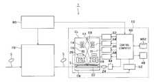
- FIG. 1is a block diagram illustrating a schematic configuration of an embodiment of a substrate inspection apparatus according to the present invention
- FIGS. 2A-2Dare diagrams illustrating specific examples of pattern defects
- FIG. 4is a diagram illustrating a first embodiment of a substrate inspection method according to the present invention.
- FIG. 6is a diagram illustrating a third embodiment of a substrate inspection method according to the present invention.
- FIG. 1is a block diagram illustrating a schematic configuration of an embodiment of a substrate inspection apparatus according to the present invention.
- a substrate inspection apparatus 1shown in FIG. 1 , comprises an electron microscope unit 10 , a film-forming device 70 and a control unit 80 .
- the film-forming device 70forms a conductive thin film, which will be described later, on an inspection target substrate S randomly extracted from an inspection lot.
- the electron microscope unit 10irradiates the inspection target substrate S having the conductive thin film formed thereon with an electron beam, and detects secondary electrons, etc., and outputs a two-dimensional inspection image.
- the electron microscope unit 10correspond to, for example, an imaging device.
- the electron microscope unit 10includes an electron beam column CL, a sample chamber CM, various electron optical system control circuits 32 , 34 , 36 and 38 , a X-Y stage 22 supporting the inspection target substrate S, a motor 24 , a stage control circuit 44 , a detector 26 , a signal processor 52 , a monitor 48 , a control computer 60 , and a type of a recording medium MR 2 that is incorporated in the apparatus in advance or is attachable/detectable to/from the apparatus.
- the present embodimentaims at obtaining an inspection image with an excellent contract resulting from a potential difference, and is an embodiment preferable for detecting large-sized defects.
- the titanium oxide (TiO 2 ) film F 10is formed on the titanium (Ti) film F 12 , the release amount of the secondary electrons, etc., can be increased compared to the case where a titanium (Ti) film, which is grounded via silicon, is formed alone, the S/N ratio of the inspection image can be improved.
- the film thickness “Ts” of the pattern side surface portion PS 16is thinner, the amount of secondary electrons, etc., released from the edge of the pattern top surface portion PT 16 is increased, so in order to generate a potential difference between the pattern top surface portion PT 16 and the pattern bottom surface portion PB 16 in a stable manner to enhance the pattern contrast, the film thickness “Ts” of the pattern side surface portion PS 16 is important. Meanwhile, when enhancing the resolution of the pattern edge portion between the pattern top surface portion PT 16 and the pattern bottom surface portion PB 16 to detect minute shape defects in the pattern periphery (outer shape), the film thickness “Tb” of the pattern bottom surface portion PB 16 is important. In order to obtain an inspection image that is excellent in potential contrast and surface shape contrast, a relationship of “Tt”>“Tb”>“Ts” can be considered to be proper.
Landscapes
- Chemical & Material Sciences (AREA)
- Analytical Chemistry (AREA)
- Physics & Mathematics (AREA)
- Engineering & Computer Science (AREA)
- Computer Vision & Pattern Recognition (AREA)
- Electromagnetism (AREA)
- General Physics & Mathematics (AREA)
- Analysing Materials By The Use Of Radiation (AREA)
Abstract
Description
Claims (18)
Applications Claiming Priority (2)
| Application Number | Priority Date | Filing Date | Title |
|---|---|---|---|
| JP2007076957AJP2008233035A (en) | 2007-03-23 | 2007-03-23 | Board inspection method |
| JP2007-076957 | 2007-03-23 |
Publications (2)
| Publication Number | Publication Date |
|---|---|
| US20080231856A1 US20080231856A1 (en) | 2008-09-25 |
| US7838831B2true US7838831B2 (en) | 2010-11-23 |
Family
ID=39774349
Family Applications (1)
| Application Number | Title | Priority Date | Filing Date |
|---|---|---|---|
| US12/053,174Active2029-02-14US7838831B2 (en) | 2007-03-23 | 2008-03-21 | Substrate inspection apparatus, substrate inspection method and semiconductor device manufacturing method |
Country Status (2)
| Country | Link |
|---|---|
| US (1) | US7838831B2 (en) |
| JP (1) | JP2008233035A (en) |
Cited By (2)
| Publication number | Priority date | Publication date | Assignee | Title |
|---|---|---|---|---|
| US20130084657A1 (en)* | 2011-09-29 | 2013-04-04 | Taiwan Semiconductor Manufacturing Company, Ltd. | Plasma Density Control |
| US20150343461A1 (en)* | 2009-06-29 | 2015-12-03 | Asml Netherlands B.V. | Deposition Method and Apparatus |
Families Citing this family (1)
| Publication number | Priority date | Publication date | Assignee | Title |
|---|---|---|---|---|
| EP2960684A1 (en)* | 2014-06-26 | 2015-12-30 | Ampass-explorer Corp. | Antenna assembly |
Citations (38)
| Publication number | Priority date | Publication date | Assignee | Title |
|---|---|---|---|---|
| US4264822A (en)* | 1978-11-27 | 1981-04-28 | Hitachi, Ltd. | Electron beam testing method and apparatus of mask |
| US4528452A (en)* | 1982-12-09 | 1985-07-09 | Electron Beam Corporation | Alignment and detection system for electron image projectors |
| US4654649A (en)* | 1982-07-20 | 1987-03-31 | Tokyo Shibaura Denki Kabushiki Kaisha | Display device |
| US4851097A (en)* | 1986-12-26 | 1989-07-25 | Seiko Instruments Inc. | Apparatus for repairing a pattern film |
| US4983830A (en)* | 1989-06-29 | 1991-01-08 | Seiko Instruments Inc. | Focused ion beam apparatus having charged particle energy filter |
| US5004927A (en)* | 1987-12-10 | 1991-04-02 | Fujitsu Limited | Process for forming a fine pattern having a high aspect ratio |
| US5022977A (en)* | 1986-09-29 | 1991-06-11 | Nippon Telegraph And Telephone Corporation | Ion generation apparatus and thin film forming apparatus and ion source utilizing the ion generation apparatus |
| US5055696A (en)* | 1988-08-29 | 1991-10-08 | Hitachi, Ltd. | Multilayered device micro etching method and system |
| JPH04242060A (en) | 1991-01-11 | 1992-08-28 | Jeol Ltd | reflection electron microscope |
| US5214282A (en)* | 1990-05-30 | 1993-05-25 | Hitachi, Ltd. | Method and apparatus for processing a minute portion of a specimen |
| US5350649A (en)* | 1988-11-22 | 1994-09-27 | Hitachi, Ltd. | Mask for manufacturing semiconductor device and method of manufacture thereof |
| US5576833A (en)* | 1994-03-11 | 1996-11-19 | Kabushiki Kaisha Toshiba | Wafer pattern defect detection method and apparatus therefor |
| US5796111A (en)* | 1995-10-30 | 1998-08-18 | Phrasor Scientific, Inc. | Apparatus for cleaning contaminated surfaces using energetic cluster beams |
| JPH11326247A (en) | 1998-05-15 | 1999-11-26 | Toshiba Corp | Substrate inspection apparatus, substrate inspection system including the same, and substrate inspection method |
| US6214738B1 (en)* | 1998-12-25 | 2001-04-10 | Canon Kabushiki Kaisha | Method for producing narrow pores and structure having the narrow pores, and narrow pores and structure produced by the method |
| US6319321B1 (en)* | 1997-01-20 | 2001-11-20 | Agency Of Industrial Science & Technology Ministry Of International Trade & Industry | Thin-film fabrication method and apparatus |
| US6548412B2 (en)* | 2001-03-19 | 2003-04-15 | National Institute For Materials Science | Method of forming patterned thin film |
| US6677587B2 (en)* | 1999-09-21 | 2004-01-13 | Nikon Corporation | Electron beam apparatus, and inspection instrument and inspection process thereof |
| US6781125B2 (en)* | 2000-11-02 | 2004-08-24 | Hitachi, Ltd. | Method and apparatus for processing a micro sample |
| JP2004354084A (en) | 2003-05-27 | 2004-12-16 | Toshiba Corp | Substrate inspection device, substrate inspection method, and semiconductor device manufacturing method |
| US6909092B2 (en)* | 2002-05-16 | 2005-06-21 | Ebara Corporation | Electron beam apparatus and device manufacturing method using same |
| US6914008B2 (en)* | 2001-05-11 | 2005-07-05 | Canon Kabushiki Kaisha | Structure having pores and its manufacturing method |
| US6914444B2 (en)* | 2000-05-30 | 2005-07-05 | Fab Solutions, Inc. | Semiconductor device test method and semiconductor device tester |
| US6949478B2 (en)* | 1991-08-19 | 2005-09-27 | Tadahiro Ohmi | Oxide film forming method |
| US6992290B2 (en)* | 2001-01-10 | 2006-01-31 | Ebara Corporation | Electron beam inspection system and inspection method and method of manufacturing devices using the system |
| US7075072B2 (en)* | 2001-09-10 | 2006-07-11 | Ebara Corporation | Detecting apparatus and device manufacturing method |
| US7212017B2 (en)* | 2003-12-25 | 2007-05-01 | Ebara Corporation | Electron beam apparatus with detailed observation function and sample inspecting and observing method using electron beam apparatus |
| US20070114463A1 (en)* | 2005-10-21 | 2007-05-24 | Tetsuro Nakasugi | Charged particle beam exposure method of character projection system, charged particle beam exposure device of character projection system, program for use in charged particle beam exposure device, and manufacturing method of semiconductor device |
| US7241993B2 (en)* | 2000-06-27 | 2007-07-10 | Ebara Corporation | Inspection system by charged particle beam and method of manufacturing devices using the system |
| US20070278419A1 (en)* | 2005-07-08 | 2007-12-06 | Nexgensemi Holdings Corporation | Apparatus and method for controlled particle beam manufacturing |
| US7323814B2 (en)* | 1999-03-05 | 2008-01-29 | Canon Kabushiki Kaisha | Image formation apparatus having fluorescent material and black material |
| US7391036B2 (en)* | 2002-04-17 | 2008-06-24 | Ebara Corporation | Sample surface inspection apparatus and method |
| US7439502B2 (en)* | 2000-11-02 | 2008-10-21 | Ebara Corporation | Electron beam apparatus and device production method using the electron beam apparatus |
| US20090042106A1 (en)* | 2003-01-31 | 2009-02-12 | Renesas Technology Corp. | Photomask, and method and apparatus for producing the same |
| JP4242060B2 (en) | 1997-08-08 | 2009-03-18 | テレフオンアクチーボラゲット エル エム エリクソン(パブル) | Method and configuration in a digital communication system |
| US20090101816A1 (en)* | 2003-04-22 | 2009-04-23 | Ebara Corporation | Testing apparatus using charged particles and device manufacturing method using the testing apparatus |
| US20090212213A1 (en)* | 2005-03-03 | 2009-08-27 | Ebara Corporation | Projection electron beam apparatus and defect inspection system using the apparatus |
| US7592586B2 (en)* | 2003-01-27 | 2009-09-22 | Ebara Corporation | Mapping-projection-type electron beam apparatus for inspecting sample by using electrons reflected from the sample |
- 2007
- 2007-03-23JPJP2007076957Apatent/JP2008233035A/ennot_activeWithdrawn
- 2008
- 2008-03-21USUS12/053,174patent/US7838831B2/enactiveActive
Patent Citations (52)
| Publication number | Priority date | Publication date | Assignee | Title |
|---|---|---|---|---|
| US4264822A (en)* | 1978-11-27 | 1981-04-28 | Hitachi, Ltd. | Electron beam testing method and apparatus of mask |
| US4654649A (en)* | 1982-07-20 | 1987-03-31 | Tokyo Shibaura Denki Kabushiki Kaisha | Display device |
| US4528452A (en)* | 1982-12-09 | 1985-07-09 | Electron Beam Corporation | Alignment and detection system for electron image projectors |
| US5022977A (en)* | 1986-09-29 | 1991-06-11 | Nippon Telegraph And Telephone Corporation | Ion generation apparatus and thin film forming apparatus and ion source utilizing the ion generation apparatus |
| US4851097A (en)* | 1986-12-26 | 1989-07-25 | Seiko Instruments Inc. | Apparatus for repairing a pattern film |
| US5004927A (en)* | 1987-12-10 | 1991-04-02 | Fujitsu Limited | Process for forming a fine pattern having a high aspect ratio |
| US5055696A (en)* | 1988-08-29 | 1991-10-08 | Hitachi, Ltd. | Multilayered device micro etching method and system |
| US5350649A (en)* | 1988-11-22 | 1994-09-27 | Hitachi, Ltd. | Mask for manufacturing semiconductor device and method of manufacture thereof |
| US5484671A (en)* | 1988-11-22 | 1996-01-16 | Hitachi, Ltd. | Mask for manufacturing semiconductor device and method of manufacture thereof |
| US4983830A (en)* | 1989-06-29 | 1991-01-08 | Seiko Instruments Inc. | Focused ion beam apparatus having charged particle energy filter |
| US5214282A (en)* | 1990-05-30 | 1993-05-25 | Hitachi, Ltd. | Method and apparatus for processing a minute portion of a specimen |
| JPH04242060A (en) | 1991-01-11 | 1992-08-28 | Jeol Ltd | reflection electron microscope |
| US6949478B2 (en)* | 1991-08-19 | 2005-09-27 | Tadahiro Ohmi | Oxide film forming method |
| US5576833A (en)* | 1994-03-11 | 1996-11-19 | Kabushiki Kaisha Toshiba | Wafer pattern defect detection method and apparatus therefor |
| US5796111A (en)* | 1995-10-30 | 1998-08-18 | Phrasor Scientific, Inc. | Apparatus for cleaning contaminated surfaces using energetic cluster beams |
| US6319321B1 (en)* | 1997-01-20 | 2001-11-20 | Agency Of Industrial Science & Technology Ministry Of International Trade & Industry | Thin-film fabrication method and apparatus |
| JP4242060B2 (en) | 1997-08-08 | 2009-03-18 | テレフオンアクチーボラゲット エル エム エリクソン(パブル) | Method and configuration in a digital communication system |
| JPH11326247A (en) | 1998-05-15 | 1999-11-26 | Toshiba Corp | Substrate inspection apparatus, substrate inspection system including the same, and substrate inspection method |
| US6541386B2 (en)* | 1998-12-25 | 2003-04-01 | Canon Kabushiki Kaisha | Method for producing a structure with narrow pores |
| US6214738B1 (en)* | 1998-12-25 | 2001-04-10 | Canon Kabushiki Kaisha | Method for producing narrow pores and structure having the narrow pores, and narrow pores and structure produced by the method |
| US7323814B2 (en)* | 1999-03-05 | 2008-01-29 | Canon Kabushiki Kaisha | Image formation apparatus having fluorescent material and black material |
| US6958477B2 (en)* | 1999-09-21 | 2005-10-25 | Nikon Corporation | Electron beam apparatus, and inspection instrument and inspection process thereof |
| US6677587B2 (en)* | 1999-09-21 | 2004-01-13 | Nikon Corporation | Electron beam apparatus, and inspection instrument and inspection process thereof |
| US6914444B2 (en)* | 2000-05-30 | 2005-07-05 | Fab Solutions, Inc. | Semiconductor device test method and semiconductor device tester |
| US20090032708A1 (en)* | 2000-06-27 | 2009-02-05 | Ebara Corporation | Inspection system by charged particle beam and method of manufacturing devices using the system |
| US7241993B2 (en)* | 2000-06-27 | 2007-07-10 | Ebara Corporation | Inspection system by charged particle beam and method of manufacturing devices using the system |
| US7411191B2 (en)* | 2000-06-27 | 2008-08-12 | Ebara Corporation | Inspection system by charged particle beam and method of manufacturing devices using the system |
| US7550750B2 (en)* | 2000-11-02 | 2009-06-23 | Hitachi, Ltd. | Method and apparatus for processing a micro sample |
| US6781125B2 (en)* | 2000-11-02 | 2004-08-24 | Hitachi, Ltd. | Method and apparatus for processing a micro sample |
| US7439502B2 (en)* | 2000-11-02 | 2008-10-21 | Ebara Corporation | Electron beam apparatus and device production method using the electron beam apparatus |
| US6992290B2 (en)* | 2001-01-10 | 2006-01-31 | Ebara Corporation | Electron beam inspection system and inspection method and method of manufacturing devices using the system |
| US20080173814A1 (en)* | 2001-01-10 | 2008-07-24 | Ebara Corporation | Electron beam inspection system and inspection method and method of manufacturing devices using the system |
| US7351969B2 (en)* | 2001-01-10 | 2008-04-01 | Ebara Corporation | Electron beam inspection system and inspection method and method of manufacturing devices using the system |
| US6548412B2 (en)* | 2001-03-19 | 2003-04-15 | National Institute For Materials Science | Method of forming patterned thin film |
| US6914008B2 (en)* | 2001-05-11 | 2005-07-05 | Canon Kabushiki Kaisha | Structure having pores and its manufacturing method |
| US7075072B2 (en)* | 2001-09-10 | 2006-07-11 | Ebara Corporation | Detecting apparatus and device manufacturing method |
| US7449691B2 (en)* | 2001-09-10 | 2008-11-11 | Ebara Corporation | Detecting apparatus and device manufacturing method |
| US20080265159A1 (en)* | 2002-04-17 | 2008-10-30 | Ebara Corporation | Sample surface inspection apparatus and method |
| US7391036B2 (en)* | 2002-04-17 | 2008-06-24 | Ebara Corporation | Sample surface inspection apparatus and method |
| US20050205783A1 (en)* | 2002-05-16 | 2005-09-22 | Ebara Corporation | Electron beam apparatus and device manufacturing method using same |
| US7098457B2 (en)* | 2002-05-16 | 2006-08-29 | Ebara Corporation | Electron beam apparatus and device manufacturing method using same |
| US6909092B2 (en)* | 2002-05-16 | 2005-06-21 | Ebara Corporation | Electron beam apparatus and device manufacturing method using same |
| US7592586B2 (en)* | 2003-01-27 | 2009-09-22 | Ebara Corporation | Mapping-projection-type electron beam apparatus for inspecting sample by using electrons reflected from the sample |
| US20100019149A1 (en)* | 2003-01-27 | 2010-01-28 | Ebara Corporation | Mapping-projection-type electron beam apparatus for inspecting sample by using electrons emitted from the sample |
| US20090042106A1 (en)* | 2003-01-31 | 2009-02-12 | Renesas Technology Corp. | Photomask, and method and apparatus for producing the same |
| US20090101816A1 (en)* | 2003-04-22 | 2009-04-23 | Ebara Corporation | Testing apparatus using charged particles and device manufacturing method using the testing apparatus |
| JP2004354084A (en) | 2003-05-27 | 2004-12-16 | Toshiba Corp | Substrate inspection device, substrate inspection method, and semiconductor device manufacturing method |
| US7212017B2 (en)* | 2003-12-25 | 2007-05-01 | Ebara Corporation | Electron beam apparatus with detailed observation function and sample inspecting and observing method using electron beam apparatus |
| US20090212213A1 (en)* | 2005-03-03 | 2009-08-27 | Ebara Corporation | Projection electron beam apparatus and defect inspection system using the apparatus |
| US20070278419A1 (en)* | 2005-07-08 | 2007-12-06 | Nexgensemi Holdings Corporation | Apparatus and method for controlled particle beam manufacturing |
| US20070278418A1 (en)* | 2005-07-08 | 2007-12-06 | Nexgensemi Holdings Corporation | Apparatus and method for controlled particle beam manufacturing |
| US20070114463A1 (en)* | 2005-10-21 | 2007-05-24 | Tetsuro Nakasugi | Charged particle beam exposure method of character projection system, charged particle beam exposure device of character projection system, program for use in charged particle beam exposure device, and manufacturing method of semiconductor device |
Non-Patent Citations (1)
| Title |
|---|
| K. Tsuno, "Simulation of a Wien filter as beam separator in a low energy electron microscope," Ultramicroscopy 55 (1994), pp. 127-140. |
Cited By (3)
| Publication number | Priority date | Publication date | Assignee | Title |
|---|---|---|---|---|
| US20150343461A1 (en)* | 2009-06-29 | 2015-12-03 | Asml Netherlands B.V. | Deposition Method and Apparatus |
| US20130084657A1 (en)* | 2011-09-29 | 2013-04-04 | Taiwan Semiconductor Manufacturing Company, Ltd. | Plasma Density Control |
| US8889435B2 (en)* | 2011-09-29 | 2014-11-18 | Taiwan Semiconductor Manufacturing Company, Ltd. | Plasma density control |
Also Published As
| Publication number | Publication date |
|---|---|
| US20080231856A1 (en) | 2008-09-25 |
| JP2008233035A (en) | 2008-10-02 |
Similar Documents
| Publication | Publication Date | Title |
|---|---|---|
| Paolillo et al. | Direct metal etch of ruthenium for advanced interconnect | |
| TW461964B (en) | Voltage contrast method and apparatus for semiconductor inspection using low voltage particle beam | |
| US6583634B1 (en) | Method of inspecting circuit pattern and inspecting instrument | |
| US8124933B2 (en) | Mapping-projection-type electron beam apparatus for inspecting sample by using electrons emitted from the sample | |
| WO2016002003A1 (en) | Substrate inspection apparatus and substrate inspection method | |
| KR102273042B1 (en) | Face-on, gas-assisted etching for plan-view lamellae preparation | |
| US20160189369A1 (en) | Method and system for detecting defects | |
| TW201907157A (en) | Method and equipment for checking the same | |
| US9190240B2 (en) | Charged particle microscope apparatus and image acquisition method of charged particle microscope apparatus utilizing image correction based on estimated diffusion of charged particles | |
| US7838831B2 (en) | Substrate inspection apparatus, substrate inspection method and semiconductor device manufacturing method | |
| US7674570B2 (en) | Mask pattern inspection method, exposure condition verification method, and manufacturing method of semiconductor device | |
| US20150116678A1 (en) | System and Method for Real-Time Overlay Error Reduction | |
| US6952105B2 (en) | Inspection method and apparatus for circuit pattern of resist material | |
| JP7664427B2 (en) | Charged particle beam device and inspection method using same | |
| US8022356B2 (en) | Sample and method for evaluating resolution of scanning electron microscope, and electron scanning microscope | |
| JP3876668B2 (en) | Visual inspection equipment using electron beam | |
| CN100590834C (en) | Substrate inspection apparatus and substrate inspection method | |
| Iida et al. | Development of standard samples with programmed defects for evaluation of pattern inspection tools for 7-nm and smaller nodes | |
| US12354833B2 (en) | Multiple landing energy scanning electron microscopy systems and methods | |
| US20080067383A1 (en) | Electron-beam size measuring apparatus and size measuring method with electron beams | |
| TW202217901A (en) | Enabling scanning electron microscope imaging while preventing sample damage on sensitive layers used in semiconductor manufacturing processes | |
| JP4060143B2 (en) | Nondestructive measuring apparatus and semiconductor device manufacturing method | |
| JP3875930B2 (en) | Electron beam apparatus and device manufacturing method using the same | |
| JP2004157135A (en) | Circuit pattern inspection method and inspection device | |
| JP2002148227A (en) | Surface inspection method and apparatus, and device manufacturing method |
Legal Events
| Date | Code | Title | Description |
|---|---|---|---|
| AS | Assignment | Owner name:KABUSHIKI KAISHA TOSHIBA, JAPAN Free format text:ASSIGNMENT OF ASSIGNORS INTEREST;ASSIGNOR:NAGAHAMA, ICHIROTA;REEL/FRAME:021028/0404 Effective date:20080509 | |
| STCF | Information on status: patent grant | Free format text:PATENTED CASE | |
| FEPP | Fee payment procedure | Free format text:PAYOR NUMBER ASSIGNED (ORIGINAL EVENT CODE: ASPN); ENTITY STATUS OF PATENT OWNER: LARGE ENTITY | |
| FPAY | Fee payment | Year of fee payment:4 | |
| AS | Assignment | Owner name:TOSHIBA MEMORY CORPORATION, JAPAN Free format text:ASSIGNMENT OF ASSIGNORS INTEREST;ASSIGNOR:KABUSHIKI KAISHA TOSHIBA;REEL/FRAME:043709/0035 Effective date:20170706 | |
| MAFP | Maintenance fee payment | Free format text:PAYMENT OF MAINTENANCE FEE, 8TH YEAR, LARGE ENTITY (ORIGINAL EVENT CODE: M1552) Year of fee payment:8 | |
| AS | Assignment | Owner name:K.K. PANGEA, JAPAN Free format text:MERGER;ASSIGNOR:TOSHIBA MEMORY CORPORATION;REEL/FRAME:055659/0471 Effective date:20180801 Owner name:TOSHIBA MEMORY CORPORATION, JAPAN Free format text:CHANGE OF NAME AND ADDRESS;ASSIGNOR:K.K. PANGEA;REEL/FRAME:055669/0401 Effective date:20180801 Owner name:KIOXIA CORPORATION, JAPAN Free format text:CHANGE OF NAME AND ADDRESS;ASSIGNOR:TOSHIBA MEMORY CORPORATION;REEL/FRAME:055669/0001 Effective date:20191001 | |
| MAFP | Maintenance fee payment | Free format text:PAYMENT OF MAINTENANCE FEE, 12TH YEAR, LARGE ENTITY (ORIGINAL EVENT CODE: M1553); ENTITY STATUS OF PATENT OWNER: LARGE ENTITY Year of fee payment:12 |