US7838420B2 - Method for forming a packaged semiconductor device - Google Patents
Method for forming a packaged semiconductor deviceDownload PDFInfo
- Publication number
- US7838420B2 US7838420B2US11/846,874US84687407AUS7838420B2US 7838420 B2US7838420 B2US 7838420B2US 84687407 AUS84687407 AUS 84687407AUS 7838420 B2US7838420 B2US 7838420B2
- Authority
- US
- United States
- Prior art keywords
- connector block
- forming
- semiconductor device
- polymer layer
- over
- Prior art date
- Legal status (The legal status is an assumption and is not a legal conclusion. Google has not performed a legal analysis and makes no representation as to the accuracy of the status listed.)
- Active, expires
Links
Images


Classifications
- H—ELECTRICITY
- H01—ELECTRIC ELEMENTS
- H01L—SEMICONDUCTOR DEVICES NOT COVERED BY CLASS H10
- H01L23/00—Details of semiconductor or other solid state devices
- H01L23/52—Arrangements for conducting electric current within the device in operation from one component to another, i.e. interconnections, e.g. wires, lead frames
- H01L23/538—Arrangements for conducting electric current within the device in operation from one component to another, i.e. interconnections, e.g. wires, lead frames the interconnection structure between a plurality of semiconductor chips being formed on, or in, insulating substrates
- H01L23/5389—Arrangements for conducting electric current within the device in operation from one component to another, i.e. interconnections, e.g. wires, lead frames the interconnection structure between a plurality of semiconductor chips being formed on, or in, insulating substrates the chips being integrally enclosed by the interconnect and support structures
- H—ELECTRICITY
- H01—ELECTRIC ELEMENTS
- H01L—SEMICONDUCTOR DEVICES NOT COVERED BY CLASS H10
- H01L21/00—Processes or apparatus adapted for the manufacture or treatment of semiconductor or solid state devices or of parts thereof
- H01L21/67—Apparatus specially adapted for handling semiconductor or electric solid state devices during manufacture or treatment thereof; Apparatus specially adapted for handling wafers during manufacture or treatment of semiconductor or electric solid state devices or components ; Apparatus not specifically provided for elsewhere
- H01L21/683—Apparatus specially adapted for handling semiconductor or electric solid state devices during manufacture or treatment thereof; Apparatus specially adapted for handling wafers during manufacture or treatment of semiconductor or electric solid state devices or components ; Apparatus not specifically provided for elsewhere for supporting or gripping
- H01L21/6835—Apparatus specially adapted for handling semiconductor or electric solid state devices during manufacture or treatment thereof; Apparatus specially adapted for handling wafers during manufacture or treatment of semiconductor or electric solid state devices or components ; Apparatus not specifically provided for elsewhere for supporting or gripping using temporarily an auxiliary support
- H—ELECTRICITY
- H01—ELECTRIC ELEMENTS
- H01L—SEMICONDUCTOR DEVICES NOT COVERED BY CLASS H10
- H01L23/00—Details of semiconductor or other solid state devices
- H01L23/28—Encapsulations, e.g. encapsulating layers, coatings, e.g. for protection
- H01L23/31—Encapsulations, e.g. encapsulating layers, coatings, e.g. for protection characterised by the arrangement or shape
- H01L23/3107—Encapsulations, e.g. encapsulating layers, coatings, e.g. for protection characterised by the arrangement or shape the device being completely enclosed
- H01L23/3121—Encapsulations, e.g. encapsulating layers, coatings, e.g. for protection characterised by the arrangement or shape the device being completely enclosed a substrate forming part of the encapsulation
- H—ELECTRICITY
- H01—ELECTRIC ELEMENTS
- H01L—SEMICONDUCTOR DEVICES NOT COVERED BY CLASS H10
- H01L23/00—Details of semiconductor or other solid state devices
- H01L23/52—Arrangements for conducting electric current within the device in operation from one component to another, i.e. interconnections, e.g. wires, lead frames
- H01L23/538—Arrangements for conducting electric current within the device in operation from one component to another, i.e. interconnections, e.g. wires, lead frames the interconnection structure between a plurality of semiconductor chips being formed on, or in, insulating substrates
- H01L23/5384—Conductive vias through the substrate with or without pins, e.g. buried coaxial conductors
- H—ELECTRICITY
- H01—ELECTRIC ELEMENTS
- H01L—SEMICONDUCTOR DEVICES NOT COVERED BY CLASS H10
- H01L23/00—Details of semiconductor or other solid state devices
- H01L23/52—Arrangements for conducting electric current within the device in operation from one component to another, i.e. interconnections, e.g. wires, lead frames
- H01L23/538—Arrangements for conducting electric current within the device in operation from one component to another, i.e. interconnections, e.g. wires, lead frames the interconnection structure between a plurality of semiconductor chips being formed on, or in, insulating substrates
- H01L23/5385—Assembly of a plurality of insulating substrates
- H—ELECTRICITY
- H01—ELECTRIC ELEMENTS
- H01L—SEMICONDUCTOR DEVICES NOT COVERED BY CLASS H10
- H01L23/00—Details of semiconductor or other solid state devices
- H01L23/58—Structural electrical arrangements for semiconductor devices not otherwise provided for, e.g. in combination with batteries
- H01L23/64—Impedance arrangements
- H01L23/66—High-frequency adaptations
- H—ELECTRICITY
- H01—ELECTRIC ELEMENTS
- H01L—SEMICONDUCTOR DEVICES NOT COVERED BY CLASS H10
- H01L24/00—Arrangements for connecting or disconnecting semiconductor or solid-state bodies; Methods or apparatus related thereto
- H01L24/01—Means for bonding being attached to, or being formed on, the surface to be connected, e.g. chip-to-package, die-attach, "first-level" interconnects; Manufacturing methods related thereto
- H01L24/18—High density interconnect [HDI] connectors; Manufacturing methods related thereto
- H01L24/19—Manufacturing methods of high density interconnect preforms
- H—ELECTRICITY
- H01—ELECTRIC ELEMENTS
- H01L—SEMICONDUCTOR DEVICES NOT COVERED BY CLASS H10
- H01L24/00—Arrangements for connecting or disconnecting semiconductor or solid-state bodies; Methods or apparatus related thereto
- H01L24/01—Means for bonding being attached to, or being formed on, the surface to be connected, e.g. chip-to-package, die-attach, "first-level" interconnects; Manufacturing methods related thereto
- H01L24/18—High density interconnect [HDI] connectors; Manufacturing methods related thereto
- H01L24/20—Structure, shape, material or disposition of high density interconnect preforms
- H—ELECTRICITY
- H01—ELECTRIC ELEMENTS
- H01L—SEMICONDUCTOR DEVICES NOT COVERED BY CLASS H10
- H01L24/00—Arrangements for connecting or disconnecting semiconductor or solid-state bodies; Methods or apparatus related thereto
- H01L24/93—Batch processes
- H01L24/95—Batch processes at chip-level, i.e. with connecting carried out on a plurality of singulated devices, i.e. on diced chips
- H01L24/96—Batch processes at chip-level, i.e. with connecting carried out on a plurality of singulated devices, i.e. on diced chips the devices being encapsulated in a common layer, e.g. neo-wafer or pseudo-wafer, said common layer being separable into individual assemblies after connecting
- H—ELECTRICITY
- H01—ELECTRIC ELEMENTS
- H01L—SEMICONDUCTOR DEVICES NOT COVERED BY CLASS H10
- H01L25/00—Assemblies consisting of a plurality of semiconductor or other solid state devices
- H01L25/03—Assemblies consisting of a plurality of semiconductor or other solid state devices all the devices being of a type provided for in a single subclass of subclasses H10B, H10D, H10F, H10H, H10K or H10N, e.g. assemblies of rectifier diodes
- H01L25/04—Assemblies consisting of a plurality of semiconductor or other solid state devices all the devices being of a type provided for in a single subclass of subclasses H10B, H10D, H10F, H10H, H10K or H10N, e.g. assemblies of rectifier diodes the devices not having separate containers
- H01L25/065—Assemblies consisting of a plurality of semiconductor or other solid state devices all the devices being of a type provided for in a single subclass of subclasses H10B, H10D, H10F, H10H, H10K or H10N, e.g. assemblies of rectifier diodes the devices not having separate containers the devices being of a type provided for in group H10D89/00
- H01L25/0655—Assemblies consisting of a plurality of semiconductor or other solid state devices all the devices being of a type provided for in a single subclass of subclasses H10B, H10D, H10F, H10H, H10K or H10N, e.g. assemblies of rectifier diodes the devices not having separate containers the devices being of a type provided for in group H10D89/00 the devices being arranged next to each other
- H—ELECTRICITY
- H01—ELECTRIC ELEMENTS
- H01L—SEMICONDUCTOR DEVICES NOT COVERED BY CLASS H10
- H01L25/00—Assemblies consisting of a plurality of semiconductor or other solid state devices
- H01L25/16—Assemblies consisting of a plurality of semiconductor or other solid state devices the devices being of types provided for in two or more different subclasses of H10B, H10D, H10F, H10H, H10K or H10N, e.g. forming hybrid circuits
- H—ELECTRICITY
- H01—ELECTRIC ELEMENTS
- H01L—SEMICONDUCTOR DEVICES NOT COVERED BY CLASS H10
- H01L21/00—Processes or apparatus adapted for the manufacture or treatment of semiconductor or solid state devices or of parts thereof
- H01L21/02—Manufacture or treatment of semiconductor devices or of parts thereof
- H01L21/04—Manufacture or treatment of semiconductor devices or of parts thereof the devices having potential barriers, e.g. a PN junction, depletion layer or carrier concentration layer
- H01L21/50—Assembly of semiconductor devices using processes or apparatus not provided for in a single one of the groups H01L21/18 - H01L21/326 or H10D48/04 - H10D48/07 e.g. sealing of a cap to a base of a container
- H01L21/56—Encapsulations, e.g. encapsulation layers, coatings
- H01L21/568—Temporary substrate used as encapsulation process aid
- H—ELECTRICITY
- H01—ELECTRIC ELEMENTS
- H01L—SEMICONDUCTOR DEVICES NOT COVERED BY CLASS H10
- H01L2221/00—Processes or apparatus adapted for the manufacture or treatment of semiconductor or solid state devices or of parts thereof covered by H01L21/00
- H01L2221/67—Apparatus for handling semiconductor or electric solid state devices during manufacture or treatment thereof; Apparatus for handling wafers during manufacture or treatment of semiconductor or electric solid state devices or components; Apparatus not specifically provided for elsewhere
- H01L2221/683—Apparatus for handling semiconductor or electric solid state devices during manufacture or treatment thereof; Apparatus for handling wafers during manufacture or treatment of semiconductor or electric solid state devices or components; Apparatus not specifically provided for elsewhere for supporting or gripping
- H01L2221/68304—Apparatus for handling semiconductor or electric solid state devices during manufacture or treatment thereof; Apparatus for handling wafers during manufacture or treatment of semiconductor or electric solid state devices or components; Apparatus not specifically provided for elsewhere for supporting or gripping using temporarily an auxiliary support
- H01L2221/68359—Apparatus for handling semiconductor or electric solid state devices during manufacture or treatment thereof; Apparatus for handling wafers during manufacture or treatment of semiconductor or electric solid state devices or components; Apparatus not specifically provided for elsewhere for supporting or gripping using temporarily an auxiliary support used as a support during manufacture of interconnect decals or build up layers
- H—ELECTRICITY
- H01—ELECTRIC ELEMENTS
- H01L—SEMICONDUCTOR DEVICES NOT COVERED BY CLASS H10
- H01L2223/00—Details relating to semiconductor or other solid state devices covered by the group H01L23/00
- H01L2223/58—Structural electrical arrangements for semiconductor devices not otherwise provided for
- H01L2223/64—Impedance arrangements
- H01L2223/66—High-frequency adaptations
- H01L2223/6605—High-frequency electrical connections
- H01L2223/6616—Vertical connections, e.g. vias
- H01L2223/6622—Coaxial feed-throughs in active or passive substrates
- H—ELECTRICITY
- H01—ELECTRIC ELEMENTS
- H01L—SEMICONDUCTOR DEVICES NOT COVERED BY CLASS H10
- H01L2223/00—Details relating to semiconductor or other solid state devices covered by the group H01L23/00
- H01L2223/58—Structural electrical arrangements for semiconductor devices not otherwise provided for
- H01L2223/64—Impedance arrangements
- H01L2223/66—High-frequency adaptations
- H01L2223/6661—High-frequency adaptations for passive devices
- H01L2223/6677—High-frequency adaptations for passive devices for antenna, e.g. antenna included within housing of semiconductor device
- H—ELECTRICITY
- H01—ELECTRIC ELEMENTS
- H01L—SEMICONDUCTOR DEVICES NOT COVERED BY CLASS H10
- H01L2224/00—Indexing scheme for arrangements for connecting or disconnecting semiconductor or solid-state bodies and methods related thereto as covered by H01L24/00
- H01L2224/01—Means for bonding being attached to, or being formed on, the surface to be connected, e.g. chip-to-package, die-attach, "first-level" interconnects; Manufacturing methods related thereto
- H01L2224/18—High density interconnect [HDI] connectors; Manufacturing methods related thereto
- H01L2224/23—Structure, shape, material or disposition of the high density interconnect connectors after the connecting process
- H01L2224/24—Structure, shape, material or disposition of the high density interconnect connectors after the connecting process of an individual high density interconnect connector
- H01L2224/241—Disposition
- H01L2224/24151—Connecting between a semiconductor or solid-state body and an item not being a semiconductor or solid-state body, e.g. chip-to-substrate, chip-to-passive
- H01L2224/24221—Connecting between a semiconductor or solid-state body and an item not being a semiconductor or solid-state body, e.g. chip-to-substrate, chip-to-passive the body and the item being stacked
- H01L2224/24225—Connecting between a semiconductor or solid-state body and an item not being a semiconductor or solid-state body, e.g. chip-to-substrate, chip-to-passive the body and the item being stacked the item being non-metallic, e.g. insulating substrate with or without metallisation
- H01L2224/24227—Connecting between a semiconductor or solid-state body and an item not being a semiconductor or solid-state body, e.g. chip-to-substrate, chip-to-passive the body and the item being stacked the item being non-metallic, e.g. insulating substrate with or without metallisation the HDI interconnect not connecting to the same level of the item at which the semiconductor or solid-state body is mounted, e.g. the semiconductor or solid-state body being mounted in a cavity or on a protrusion of the item
- H—ELECTRICITY
- H01—ELECTRIC ELEMENTS
- H01L—SEMICONDUCTOR DEVICES NOT COVERED BY CLASS H10
- H01L2224/00—Indexing scheme for arrangements for connecting or disconnecting semiconductor or solid-state bodies and methods related thereto as covered by H01L24/00
- H01L2224/01—Means for bonding being attached to, or being formed on, the surface to be connected, e.g. chip-to-package, die-attach, "first-level" interconnects; Manufacturing methods related thereto
- H01L2224/18—High density interconnect [HDI] connectors; Manufacturing methods related thereto
- H01L2224/23—Structure, shape, material or disposition of the high density interconnect connectors after the connecting process
- H01L2224/25—Structure, shape, material or disposition of the high density interconnect connectors after the connecting process of a plurality of high density interconnect connectors
- H01L2224/251—Disposition
- H01L2224/2518—Disposition being disposed on at least two different sides of the body, e.g. dual array
- H—ELECTRICITY
- H01—ELECTRIC ELEMENTS
- H01L—SEMICONDUCTOR DEVICES NOT COVERED BY CLASS H10
- H01L23/00—Details of semiconductor or other solid state devices
- H01L23/28—Encapsulations, e.g. encapsulating layers, coatings, e.g. for protection
- H01L23/31—Encapsulations, e.g. encapsulating layers, coatings, e.g. for protection characterised by the arrangement or shape
- H01L23/3107—Encapsulations, e.g. encapsulating layers, coatings, e.g. for protection characterised by the arrangement or shape the device being completely enclosed
- H01L23/3114—Encapsulations, e.g. encapsulating layers, coatings, e.g. for protection characterised by the arrangement or shape the device being completely enclosed the device being a chip scale package, e.g. CSP
- H—ELECTRICITY
- H01—ELECTRIC ELEMENTS
- H01L—SEMICONDUCTOR DEVICES NOT COVERED BY CLASS H10
- H01L23/00—Details of semiconductor or other solid state devices
- H01L23/58—Structural electrical arrangements for semiconductor devices not otherwise provided for, e.g. in combination with batteries
- H01L23/64—Impedance arrangements
- H01L23/645—Inductive arrangements
- H—ELECTRICITY
- H01—ELECTRIC ELEMENTS
- H01L—SEMICONDUCTOR DEVICES NOT COVERED BY CLASS H10
- H01L2924/00—Indexing scheme for arrangements or methods for connecting or disconnecting semiconductor or solid-state bodies as covered by H01L24/00
- H01L2924/01—Chemical elements
- H01L2924/01015—Phosphorus [P]
- H—ELECTRICITY
- H01—ELECTRIC ELEMENTS
- H01L—SEMICONDUCTOR DEVICES NOT COVERED BY CLASS H10
- H01L2924/00—Indexing scheme for arrangements or methods for connecting or disconnecting semiconductor or solid-state bodies as covered by H01L24/00
- H01L2924/01—Chemical elements
- H01L2924/01029—Copper [Cu]
- H—ELECTRICITY
- H01—ELECTRIC ELEMENTS
- H01L—SEMICONDUCTOR DEVICES NOT COVERED BY CLASS H10
- H01L2924/00—Indexing scheme for arrangements or methods for connecting or disconnecting semiconductor or solid-state bodies as covered by H01L24/00
- H01L2924/01—Chemical elements
- H01L2924/01033—Arsenic [As]
- H—ELECTRICITY
- H01—ELECTRIC ELEMENTS
- H01L—SEMICONDUCTOR DEVICES NOT COVERED BY CLASS H10
- H01L2924/00—Indexing scheme for arrangements or methods for connecting or disconnecting semiconductor or solid-state bodies as covered by H01L24/00
- H01L2924/01—Chemical elements
- H01L2924/01047—Silver [Ag]
- H—ELECTRICITY
- H01—ELECTRIC ELEMENTS
- H01L—SEMICONDUCTOR DEVICES NOT COVERED BY CLASS H10
- H01L2924/00—Indexing scheme for arrangements or methods for connecting or disconnecting semiconductor or solid-state bodies as covered by H01L24/00
- H01L2924/01—Chemical elements
- H01L2924/01078—Platinum [Pt]
- H—ELECTRICITY
- H01—ELECTRIC ELEMENTS
- H01L—SEMICONDUCTOR DEVICES NOT COVERED BY CLASS H10
- H01L2924/00—Indexing scheme for arrangements or methods for connecting or disconnecting semiconductor or solid-state bodies as covered by H01L24/00
- H01L2924/01—Chemical elements
- H01L2924/01079—Gold [Au]
- H—ELECTRICITY
- H01—ELECTRIC ELEMENTS
- H01L—SEMICONDUCTOR DEVICES NOT COVERED BY CLASS H10
- H01L2924/00—Indexing scheme for arrangements or methods for connecting or disconnecting semiconductor or solid-state bodies as covered by H01L24/00
- H01L2924/01—Chemical elements
- H01L2924/01082—Lead [Pb]
- H—ELECTRICITY
- H01—ELECTRIC ELEMENTS
- H01L—SEMICONDUCTOR DEVICES NOT COVERED BY CLASS H10
- H01L2924/00—Indexing scheme for arrangements or methods for connecting or disconnecting semiconductor or solid-state bodies as covered by H01L24/00
- H01L2924/10—Details of semiconductor or other solid state devices to be connected
- H01L2924/11—Device type
- H01L2924/12—Passive devices, e.g. 2 terminal devices
- H01L2924/1204—Optical Diode
- H01L2924/12044—OLED
- H—ELECTRICITY
- H01—ELECTRIC ELEMENTS
- H01L—SEMICONDUCTOR DEVICES NOT COVERED BY CLASS H10
- H01L2924/00—Indexing scheme for arrangements or methods for connecting or disconnecting semiconductor or solid-state bodies as covered by H01L24/00
- H01L2924/10—Details of semiconductor or other solid state devices to be connected
- H01L2924/11—Device type
- H01L2924/14—Integrated circuits
- H—ELECTRICITY
- H01—ELECTRIC ELEMENTS
- H01L—SEMICONDUCTOR DEVICES NOT COVERED BY CLASS H10
- H01L2924/00—Indexing scheme for arrangements or methods for connecting or disconnecting semiconductor or solid-state bodies as covered by H01L24/00
- H01L2924/19—Details of hybrid assemblies other than the semiconductor or other solid state devices to be connected
- H01L2924/191—Disposition
- H01L2924/19101—Disposition of discrete passive components
- H01L2924/19105—Disposition of discrete passive components in a side-by-side arrangement on a common die mounting substrate
Definitions
- This disclosurerelates generally to packages that have more than one element including at least one semiconductor device, and more specifically, to interconnect for such packages.
- RCPredistributed chip package
- FIG. 1is a cross section of a packaged semiconductor device at a stage in processing according to an embodiment
- FIG. 2is a cross section of the packaged semiconductor device of FIG. 1 at a subsequent stage in processing
- FIG. 3is a cross section of the packaged semiconductor device of FIG. 2 at a subsequent stage in processing
- FIG. 4is a cross section of the packaged semiconductor device of FIG. 3 at a subsequent stage in processing
- FIG. 5is a cross section of the packaged semiconductor device of FIG. 4 at a subsequent stage in processing
- FIG. 6is a cross section of the packaged semiconductor device of FIG. 5 at a subsequent stage in processing
- FIG. 7is a cross section of the packaged semiconductor device of FIG. 6 at a subsequent stage in processing
- FIG. 8is a cross section of the packaged semiconductor device of FIG. 7 at a subsequent stage in processing
- FIG. 9is a cross section of the packaged semiconductor device of FIG. 8 at a subsequent stage in processing
- FIG. 10is a top view of a portion of the packaged device of FIGS. 1-9 ;
- FIG. 11is a top view of an alternative for the portion of FIG. 10 .
- connection blockwhich provides the capability of extending from the top side to a back side because the connection block is prefabricated.
- the connection blockwhich can also be called a connector block, has the organic fill formed around in the same manner as the other elements in the RCP.
- the connection blockthus allows electrical connection to be made from the interconnect on the top side to the back side without having to etch via holes and then filling the via holes to form vias.
- the distance from the top side to the back side, for practical production,is too long for forming and filling vias.
- One application of connection blockis to place an antenna on the back side. Another is place a ground plane on the back side. This is better understood by reference to the drawings and the following description.
- FIG. 1Shown in FIG. 1 is a package 10 comprising a carrier 12 , a tape 14 , an element 16 , an element 18 , and connection block 20 .
- Carrier 12is for providing mechanical support.
- Tape 14is two-sided.
- Element 16may be an integrated circuit, and element 18 may be an integrated circuit. On or the other could also be another type of element such as a passive device or a discrete semiconductor device.
- Connection block 20has a conductor 22 , a conductor 24 , and a conductor 26 that run vertically the length connection block 20 and are surrounded by a dielectric 28 .
- Dielectric 28is preferably an organic material similar to or the same as that used as the fill in making an RCP, but dielectric 28 could also be another material such as ceramic.
- connection block 20is chosen to be a little thicker than the thickness of the organic layer that surround the elements of the finished RCP. A common thickness for the organic layer surrounding the elements is about 0.65 millimeter (mm) but this may vary. In such case of 0.65 mm, connection block 20 and thus conductors 22 , 24 , and 26 are about 0.70 mm in length. Connection block 20 is preferably one mm or more in diameter. A smaller diameter may present difficulties in adhering reliably to tape 14 but may nonetheless be advantageous for some applications.
- Organic layer 30Shown in FIG. 2 is package 10 after deposition of an organic layer 30 which covers elements 16 and 18 and connection block 20 .
- Organic layer 30may be deposited to be about 0.80 mm for the example of connection block 20 being about 0.70 mm.
- Organic layer 30may be considered a polymer layer.
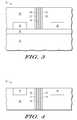
- FIG. 3Shown in FIG. 3 is package 10 after grinding organic layer 30 and a small portion of connection block 20 to expose conductors 22 , 24 , and 26 .
- Organic layer 30is then reduced, in this example, to 0.65 mm.
- FIG. 4Shown in FIG. 4 is package 10 after removing carrier 12 and tape 14 .
- FIG. 4also has package 10 inverted from that of FIGS. 1-3 .
- Elements 16 and 18are exposed on the top side of package 10 .
- the exposed surface of element 16 and the expose surface of element 18are where contacts for elements 16 and 18 reside.
- Interconnect 32may be made of multiple conductive layers connected to elements 16 and 18 and connection block 20 using vias.
- On interconnect 32is a plurality of pads 34 of which one is pad 36 .
- Pads 34are for receiving solder balls and are on a top side of package 10 .
- Connection block 20is exposed on a back side of package 10 . In a conventional RCP which would not have connection block 20 , processing could be complete except for the solder balls. Solder balls could be added at this point or at a subsequent convenient time.
- Dielectric layer 38is preferably the same material as organic layer 30 but could be another insulating material. Dielectric layer 38 may be 0.1 mm thick. Via 42 is in contact with conductor 22 . Via 44 is contact with conductor 24 . Via 46 is in contact with conductor 46 .
- FIG. 6also shows package 10 inverted from FIGS. 4 and 5 . The side with pads 34 is still called the top side though and the side with dielectric layer 38 is still called the back side.
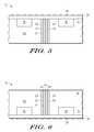
- FIG. 7Shown in FIG. 7 is package 10 after forming a patterned conductive layer over dielectric layer 38 comprising a ground plane 47 in contact with via 40 , a trace 48 on in contact with via 42 , and a trace 50 in contact with via 44 .
- Ground plane 47surrounds traces 48 and 50 .
- Trace 48extends laterally from via 42 and is present for stability.
- trace 50extends laterally from via 44 in a different direction from that of trace 48 so that the lateral extension is not visible in the cross section of FIG. 7 .
- the patterned conductive layermay be made by a conventional plating process in which a thin seed layer is deposited followed by photoresist which is patterned.
- ground plane 47 and traces 48 and 50may be about 0.10 mm.
- Dielectric layer 52may be the same material as for dielectric layer 38 .
- Via 54is in contact with trace 48 .
- Via 56is contact with trace 50 .
- via 56is shown in the cross section of FIG. 8 in contact with trace 50 , via 56 is preferably located over a wider portion of trace 50 than shown.
- FIG. 9Shown in FIG. 9 is package 10 after forming an antenna 58 in contact with vias 54 and 56 .
- Antenna 58may be formed and patterned using the same plating technique described for ground plane 47 and traces 48 and 50 .
- Antenna 58may be 0.200 mm thick.
- antenna 58 in contact with vias 54 and 56antenna is coupled to conductors 22 and 24 , respectively. Due to the high frequencies that may be involved, vias 54 and 56 may not have to be in actual contact with antenna 58 , if sufficiently close to antenna 58 , for antenna 58 to be coupled to conductor 22 .
- Package 10 of FIG. 9is a completed RCP that will have solder balls added later at a time closer to being mounted on a circuit board.
- connection block 20Shown in FIG. 10 is a top view of connection block 20 showing conductors 22 , 24 , and 26 in a line and dielectric 28 surrounding them in a circular shape.
- connection block 20is a cylinder with three inline conductors.
- Conductors 22 , 24 , and 26could be in a different configuration. Also the shape could be different than circular, such as square, rectangular, or triangular.
- connection block 60comprising an outer insulating layer 68 , a conductor ring 62 , an inner conductor 64 , and an insulating layer between conductor ring 62 and inner conductor 64 .
- Thisforms a coaxial line which may be particularly beneficial when coupling to an antenna that is transmitting and receiving RF.
- Connection block 60may replace connection block 20 with respect to the connection to antenna 58 . If a ground plane were still desirable, the connection to the ground plane could be by another connection block or connection block 60 could be modified to have another conductor outside ring 62 for coupling to the ground plane.
- connection blocksuch as connection block 20 or connection block 60 may be achieved using wire bond machines.
- a wire bondis commonly 25 microns in diameter. Three of those wire bonds can be placed into a cylindrical mold that is many times longer than that of connection block 20 .
- the moldis filled with the desired dielectric such as the material used for dielectric 30 .
- the resulting structureis then cut into pieces of the desired length of about 0.070 mm.
- the surrounding dielectricmay be a material such as ceramic. The rigidity of ceramic may be beneficial in the manufacturing process.
- a packaged semiconductor devicehaving an interconnect layer, a semiconductor device, a first conductive element, and a connector block.
- the interconnect layeris over a first side of a polymer layer.
- the semiconductor deviceis surrounded on at least three sides by the polymer layer and is coupled to the interconnect layer.
- the first conductive elementis over a second side of the polymer layer. The second side is opposite the first side.
- the connector blockis within the polymer layer and has at least one electrical path extending from a first surface of the connector block to a second surface of the connector block, and electrically couples the interconnect layer to the first conductive element through the at least one electrical path.
- the connector blockmay comprise an insulating material surrounding the at least one electrical path.
- the connector blockmay have at least two coaxial electrical paths.
- the at least one electrical pathmay be a ground path and the first conductive element may be a ground plane.
- the at least one electrical pathmay be a signal path and the first conductive element may be an antenna.
- the packaged semiconductor devicemay further comprise a second conductive element and a second electrical path, wherein the second electrical path is a ground path and the second conductive element is a ground plane.
- the packaged semiconductor devicemay further comprise a third electrical path, wherein the third electrical path is coupled to the antenna.
- the methodincludes surrounding a semiconductor device on at least three sides by a polymer layer.
- the methodfurther includes forming an interconnect layer over a first side of the polymer layer and over the semiconductor device, wherein the semiconductor device is coupled to the interconnect layer.
- the methodfurther includes forming a conductive element over a second side of the polymer layer, wherein the second side is opposite the first side.
- the methodfurther includes electrically coupling the interconnect layer to the conductive element through a connector block within the polymer layer, having at least one electrical path.
- the forming the conductive element over a second sidemay comprise plating a conductive material to form an antenna.
- the step of surroundingmay comprise attaching a semiconductor device to a temporary support structure, forming the polymer layer over the semiconductor device, and removing the temporary support structure after forming the polymer layer.
- the step of electrically couplingmay comprise attaching the connector block to the temporary support structure before forming the polymer layer, removing a portion of the polymer layer to expose a surface of the connector block, forming the interconnect layer over the surface of the connector block while forming the interconnect layer over the first side of the polymer layer.
- the methodmay further comprise depositing a dielectric layer over the surface of the connector block, and forming a via in the dielectric layer, wherein the via is electrically coupled to the connector block and the conductive element.
- the at least one electrical pathmay be selected from the group consisting of a ground path and a signal path.
- the first conductive elementmay be selected from a group consisting of a ground plane and an antenna.
- the at least one electrical pathmay comprise at least two coaxial electrical paths.
- the methodincludes attaching a semiconductor device to a temporary support structure.
- the methodfurther includes attaching a connector block to the temporary support structure, wherein the connector block has at least one electrical path.
- the methodfurther includes forming an encapsulant over the connector block and the semiconductor device.
- the methodfurther includes removing a portion of the encapsulant to expose a top surface of the connector block.
- the methodfurther includes forming an interconnect layer electrically coupled to the top surface of the connector block.
- the methodfurther includes removing the temporary support structure to expose a bottom surface of the connector block.
- the methodfurther includes electrically coupling a tangible element to the bottom surface of the connector block.
- the step of electrically coupling a tangible element to the bottom surface of the connector blockmay comprise plating a conductive material to form an antenna.
- the step of electrically coupling a tangible element to the bottom surface of the connector blockmay further comprise depositing a dielectric layer over the bottom surface of the connector block, and forming a via in the dielectric layer, wherein the via is electrically coupled to the connector block and the antenna.
- the step of removing a portion of the encapsulant to expose a top surface of the connector blockmay comprise grinding the encapsulant.
- the temporary support structuremay be selected from a group consisting of a tape and a carrier.
- the connector blockmay have at least two coaxial electrical paths.
- dielectric layer 38is shown as being formed after interconnect layer 32 whereas dielectric layer 38 may be deposited before interconnect layer 32 is formed.
- platingwas described as the method for forming patterned metal layers, but other deposition techniques may be used.
- the metalcould be sputtered and then patterned with an etch. Accordingly, the specification and figures are to be regarded in an illustrative rather than a restrictive sense, and all such modifications are intended to be included within the scope of the present invention. Any benefits, advantages, or solutions to problems that are described herein with regard to specific embodiments are not intended to be construed as a critical, required, or essential feature or element of any or all the claims.
- Coupledis not intended to be limited to a direct coupling or a mechanical coupling.
Landscapes
- Engineering & Computer Science (AREA)
- Microelectronics & Electronic Packaging (AREA)
- Power Engineering (AREA)
- Computer Hardware Design (AREA)
- Physics & Mathematics (AREA)
- Condensed Matter Physics & Semiconductors (AREA)
- General Physics & Mathematics (AREA)
- Manufacturing & Machinery (AREA)
- Internal Circuitry In Semiconductor Integrated Circuit Devices (AREA)
- Variable-Direction Aerials And Aerial Arrays (AREA)
- Details Of Aerials (AREA)
Abstract
Description
Claims (13)
Priority Applications (7)
| Application Number | Priority Date | Filing Date | Title |
|---|---|---|---|
| US11/846,874US7838420B2 (en) | 2007-08-29 | 2007-08-29 | Method for forming a packaged semiconductor device |
| JP2010522993AJP5397962B2 (en) | 2007-08-29 | 2008-07-09 | Method for forming a semiconductor device package |
| CN200880104602.4ACN101790788A (en) | 2007-08-29 | 2008-07-09 | Interconnection in the multicomponent encapsulation |
| PCT/US2008/069516WO2009032398A1 (en) | 2007-08-29 | 2008-07-09 | Interconnect in a multi-element package |
| EP08781552AEP2195840A4 (en) | 2007-08-29 | 2008-07-09 | Interconnect in a multi-element package |
| KR1020107004435AKR20100065305A (en) | 2007-08-29 | 2008-07-09 | Interconnect in a multi-element package |
| TW097126735ATWI451551B (en) | 2007-08-29 | 2008-07-15 | Interconnect in a multi-element package |
Applications Claiming Priority (1)
| Application Number | Priority Date | Filing Date | Title |
|---|---|---|---|
| US11/846,874US7838420B2 (en) | 2007-08-29 | 2007-08-29 | Method for forming a packaged semiconductor device |
Publications (2)
| Publication Number | Publication Date |
|---|---|
| US20090057849A1 US20090057849A1 (en) | 2009-03-05 |
| US7838420B2true US7838420B2 (en) | 2010-11-23 |
Family
ID=40406108
Family Applications (1)
| Application Number | Title | Priority Date | Filing Date |
|---|---|---|---|
| US11/846,874Active2028-11-08US7838420B2 (en) | 2007-08-29 | 2007-08-29 | Method for forming a packaged semiconductor device |
Country Status (7)
| Country | Link |
|---|---|
| US (1) | US7838420B2 (en) |
| EP (1) | EP2195840A4 (en) |
| JP (1) | JP5397962B2 (en) |
| KR (1) | KR20100065305A (en) |
| CN (1) | CN101790788A (en) |
| TW (1) | TWI451551B (en) |
| WO (1) | WO2009032398A1 (en) |
Cited By (9)
| Publication number | Priority date | Publication date | Assignee | Title |
|---|---|---|---|---|
| US8597983B2 (en) | 2011-11-18 | 2013-12-03 | Freescale Semiconductor, Inc. | Semiconductor device packaging having substrate with pre-encapsulation through via formation |
| US8822268B1 (en) | 2013-07-17 | 2014-09-02 | Freescale Semiconductor, Inc. | Redistributed chip packages containing multiple components and methods for the fabrication thereof |
| US8916421B2 (en) | 2011-08-31 | 2014-12-23 | Freescale Semiconductor, Inc. | Semiconductor device packaging having pre-encapsulation through via formation using lead frames with attached signal conduits |
| US9142502B2 (en) | 2011-08-31 | 2015-09-22 | Zhiwei Gong | Semiconductor device packaging having pre-encapsulation through via formation using drop-in signal conduits |
| US9362234B2 (en) | 2014-01-07 | 2016-06-07 | Freescale Semiconductor, Inc. | Shielded device packages having antennas and related fabrication methods |
| US10236260B2 (en) | 2016-06-30 | 2019-03-19 | Nxp Usa, Inc. | Shielded package with integrated antenna |
| US10354958B2 (en) | 2014-10-01 | 2019-07-16 | Nxp Usa, Inc. | Through package circuit in fan-out wafer level package |
| US11502054B2 (en) | 2020-11-11 | 2022-11-15 | Nxp Usa, Inc. | Semiconductor device assembly and method therefor |
| US11557565B2 (en) | 2020-10-06 | 2023-01-17 | Nxp Usa, Inc. | Semiconductor device assembly and method therefor |
Families Citing this family (14)
| Publication number | Priority date | Publication date | Assignee | Title |
|---|---|---|---|---|
| JP2010245107A (en)* | 2009-04-01 | 2010-10-28 | Shinko Electric Ind Co Ltd | Semiconductor device and manufacturing method thereof |
| US8407890B2 (en)* | 2010-01-25 | 2013-04-02 | Freescale Semiconductor Inc. | Method of manufacting an electronic device module with integrated antenna structure |
| JP5834907B2 (en)* | 2011-12-28 | 2015-12-24 | 富士通株式会社 | Semiconductor device, semiconductor device manufacturing method, and electronic device |
| US9842798B2 (en) | 2012-03-23 | 2017-12-12 | STATS ChipPAC Pte. Ltd. | Semiconductor device and method of forming a PoP device with embedded vertical interconnect units |
| US10049964B2 (en) | 2012-03-23 | 2018-08-14 | STATS ChipPAC Pte. Ltd. | Semiconductor device and method of forming a fan-out PoP device with PWB vertical interconnect units |
| US8810024B2 (en)* | 2012-03-23 | 2014-08-19 | Stats Chippac Ltd. | Semiconductor method and device of forming a fan-out PoP device with PWB vertical interconnect units |
| US9837303B2 (en) | 2012-03-23 | 2017-12-05 | STATS ChipPAC Pte. Ltd. | Semiconductor method and device of forming a fan-out device with PWB vertical interconnect units |
| CN103311141B (en)* | 2013-07-05 | 2016-01-20 | 北京理工大学 | A kind of manufacture method of coaxial vertical interconnection conductor |
| US9666930B2 (en) | 2014-10-23 | 2017-05-30 | Nxp Usa, Inc. | Interface between a semiconductor die and a waveguide, where the interface is covered by a molding compound |
| TWI652775B (en) | 2016-01-11 | 2019-03-01 | 矽品精密工業股份有限公司 | Electronic package |
| CN111034376B (en)* | 2017-08-21 | 2023-02-21 | 株式会社村田制作所 | Method for manufacturing electronic component and electronic component |
| CN114243287B (en)* | 2021-12-10 | 2025-08-29 | 上海微波技术研究所(中国电子科技集团公司第五十研究所) | Millimeter wave phased array antenna array integrated adapter |
| US20240088068A1 (en)* | 2022-09-08 | 2024-03-14 | Nxp Usa, Inc. | Semiconductor device with through package via and method therefor |
| US20250218977A1 (en)* | 2023-12-29 | 2025-07-03 | International Business Machines Corporation | Coaxial through insulator via between chiplets |
Citations (12)
| Publication number | Priority date | Publication date | Assignee | Title |
|---|---|---|---|---|
| US5949030A (en)* | 1997-11-14 | 1999-09-07 | International Business Machines Corporation | Vias and method for making the same in organic board and chip carriers |
| US6054389A (en)* | 1997-12-29 | 2000-04-25 | Vanguard International Semiconductor Corporation | Method of forming metal conducting pillars |
| US20020155692A1 (en) | 2000-06-16 | 2002-10-24 | Chartered Semiconductor Manufacturing Ltd. | Three dimensional TC package module |
| US6593644B2 (en) | 2001-04-19 | 2003-07-15 | International Business Machines Corporation | System of a package fabricated on a semiconductor or dielectric wafer with wiring on one face, vias extending through the wafer, and external connections on the opposing face |
| US6753600B1 (en) | 2003-01-28 | 2004-06-22 | Thin Film Module, Inc. | Structure of a substrate for a high density semiconductor package |
| US6838776B2 (en) | 2003-04-18 | 2005-01-04 | Freescale Semiconductor, Inc. | Circuit device with at least partial packaging and method for forming |
| US6921975B2 (en) | 2003-04-18 | 2005-07-26 | Freescale Semiconductor, Inc. | Circuit device with at least partial packaging, exposed active surface and a voltage reference plane |
| US20050161789A1 (en) | 2004-01-23 | 2005-07-28 | Steven Towle | Package substrate pattern to accommodate optical waveguide |
| US20050167797A1 (en) | 2004-01-29 | 2005-08-04 | Advanpack Solutions Pte Ltd | Structure package |
| US6931725B2 (en)* | 1999-12-20 | 2005-08-23 | Matsushita Electric Industrial Co., Ltd. | Circuit component built-in module, radio device having the same, and method for producing the same |
| US20060226415A1 (en)* | 2004-11-22 | 2006-10-12 | Masaaki Nishijima | Semiconductor integrated circuit device and vehicle-mounted radar system using the same |
| US7312528B2 (en)* | 2003-02-18 | 2007-12-25 | Hitachi Maxell, Ltd. | Semiconductor device having antenna connection electrodes |
Family Cites Families (14)
| Publication number | Priority date | Publication date | Assignee | Title |
|---|---|---|---|---|
| JPS56115553A (en)* | 1980-02-18 | 1981-09-10 | Fujitsu Ltd | Method of mounting integrated circuit |
| JPH10303363A (en)* | 1997-04-30 | 1998-11-13 | Sony Corp | Electronic component and manufacture therefor |
| US6081989A (en)* | 1998-04-30 | 2000-07-04 | Lockheed Martin Corporation | Fabrication of circuit modules with a transmission line |
| JP2000252407A (en)* | 1999-03-04 | 2000-09-14 | Hitachi Ltd | Multi-chip module |
| JP2001094034A (en)* | 1999-09-27 | 2001-04-06 | Nec Eng Ltd | Hybrid ic package |
| JP2002343927A (en)* | 2000-07-12 | 2002-11-29 | Hitachi Maxell Ltd | Semiconductor module and manufacturing method thereof |
| US7190080B1 (en) | 2000-10-13 | 2007-03-13 | Bridge Semiconductor Corporation | Semiconductor chip assembly with embedded metal pillar |
| JP2002184934A (en)* | 2000-12-13 | 2002-06-28 | Shinko Electric Ind Co Ltd | Semiconductor device and manufacturing method thereof |
| JP2003188340A (en)* | 2001-12-19 | 2003-07-04 | Matsushita Electric Ind Co Ltd | Component built-in module and manufacturing method thereof |
| JP2004327641A (en)* | 2003-04-24 | 2004-11-18 | Tdk Corp | Electronic component module |
| DE10320646A1 (en)* | 2003-05-07 | 2004-09-16 | Infineon Technologies Ag | Electronic component, typically integrated circuit, system support and manufacturing method, with support containing component positions in lines and columns, starting with coating auxiliary support with photosensitive layer |
| JP2005033141A (en)* | 2003-07-11 | 2005-02-03 | Sony Corp | Semiconductor device, its manufacturing method, false wafer, its manufacturing method, and packaging structure of semiconductor device |
| JP4615962B2 (en)* | 2004-10-22 | 2011-01-19 | ルネサスエレクトロニクス株式会社 | Semiconductor device |
| JP4766049B2 (en)* | 2005-09-20 | 2011-09-07 | 株式会社村田製作所 | Manufacturing method of component built-in module and component built-in module |
- 2007
- 2007-08-29USUS11/846,874patent/US7838420B2/enactiveActive
- 2008
- 2008-07-09JPJP2010522993Apatent/JP5397962B2/enactiveActive
- 2008-07-09CNCN200880104602.4Apatent/CN101790788A/enactivePending
- 2008-07-09KRKR1020107004435Apatent/KR20100065305A/ennot_activeWithdrawn
- 2008-07-09WOPCT/US2008/069516patent/WO2009032398A1/enactiveApplication Filing
- 2008-07-09EPEP08781552Apatent/EP2195840A4/ennot_activeCeased
- 2008-07-15TWTW097126735Apatent/TWI451551B/enactive
Patent Citations (12)
| Publication number | Priority date | Publication date | Assignee | Title |
|---|---|---|---|---|
| US5949030A (en)* | 1997-11-14 | 1999-09-07 | International Business Machines Corporation | Vias and method for making the same in organic board and chip carriers |
| US6054389A (en)* | 1997-12-29 | 2000-04-25 | Vanguard International Semiconductor Corporation | Method of forming metal conducting pillars |
| US6931725B2 (en)* | 1999-12-20 | 2005-08-23 | Matsushita Electric Industrial Co., Ltd. | Circuit component built-in module, radio device having the same, and method for producing the same |
| US20020155692A1 (en) | 2000-06-16 | 2002-10-24 | Chartered Semiconductor Manufacturing Ltd. | Three dimensional TC package module |
| US6593644B2 (en) | 2001-04-19 | 2003-07-15 | International Business Machines Corporation | System of a package fabricated on a semiconductor or dielectric wafer with wiring on one face, vias extending through the wafer, and external connections on the opposing face |
| US6753600B1 (en) | 2003-01-28 | 2004-06-22 | Thin Film Module, Inc. | Structure of a substrate for a high density semiconductor package |
| US7312528B2 (en)* | 2003-02-18 | 2007-12-25 | Hitachi Maxell, Ltd. | Semiconductor device having antenna connection electrodes |
| US6838776B2 (en) | 2003-04-18 | 2005-01-04 | Freescale Semiconductor, Inc. | Circuit device with at least partial packaging and method for forming |
| US6921975B2 (en) | 2003-04-18 | 2005-07-26 | Freescale Semiconductor, Inc. | Circuit device with at least partial packaging, exposed active surface and a voltage reference plane |
| US20050161789A1 (en) | 2004-01-23 | 2005-07-28 | Steven Towle | Package substrate pattern to accommodate optical waveguide |
| US20050167797A1 (en) | 2004-01-29 | 2005-08-04 | Advanpack Solutions Pte Ltd | Structure package |
| US20060226415A1 (en)* | 2004-11-22 | 2006-10-12 | Masaaki Nishijima | Semiconductor integrated circuit device and vehicle-mounted radar system using the same |
Non-Patent Citations (2)
| Title |
|---|
| International Search Report issued in corresponding PCT Application No. PCT/US2008/069516 mailed on Jan. 30, 2009. |
| Keser et al; "The Redistributed Chip Package: A Breakthrough for Advanced Packaging" Electronic COmponents and Technology Conference, 2007. ECTC '07. Proceedings. 57th; May 29, 2007-Jun. 1, 2007 pp. 286-291. |
Cited By (10)
| Publication number | Priority date | Publication date | Assignee | Title |
|---|---|---|---|---|
| US8916421B2 (en) | 2011-08-31 | 2014-12-23 | Freescale Semiconductor, Inc. | Semiconductor device packaging having pre-encapsulation through via formation using lead frames with attached signal conduits |
| US9142502B2 (en) | 2011-08-31 | 2015-09-22 | Zhiwei Gong | Semiconductor device packaging having pre-encapsulation through via formation using drop-in signal conduits |
| US8597983B2 (en) | 2011-11-18 | 2013-12-03 | Freescale Semiconductor, Inc. | Semiconductor device packaging having substrate with pre-encapsulation through via formation |
| US8822268B1 (en) | 2013-07-17 | 2014-09-02 | Freescale Semiconductor, Inc. | Redistributed chip packages containing multiple components and methods for the fabrication thereof |
| US9362234B2 (en) | 2014-01-07 | 2016-06-07 | Freescale Semiconductor, Inc. | Shielded device packages having antennas and related fabrication methods |
| US10354958B2 (en) | 2014-10-01 | 2019-07-16 | Nxp Usa, Inc. | Through package circuit in fan-out wafer level package |
| US10236260B2 (en) | 2016-06-30 | 2019-03-19 | Nxp Usa, Inc. | Shielded package with integrated antenna |
| US11557565B2 (en) | 2020-10-06 | 2023-01-17 | Nxp Usa, Inc. | Semiconductor device assembly and method therefor |
| US11502054B2 (en) | 2020-11-11 | 2022-11-15 | Nxp Usa, Inc. | Semiconductor device assembly and method therefor |
| US12027485B2 (en) | 2020-11-11 | 2024-07-02 | Nxp Usa, Inc. | Semiconductor device assembly and method therefor |
Also Published As
| Publication number | Publication date |
|---|---|
| KR20100065305A (en) | 2010-06-16 |
| WO2009032398A1 (en) | 2009-03-12 |
| US20090057849A1 (en) | 2009-03-05 |
| EP2195840A1 (en) | 2010-06-16 |
| EP2195840A4 (en) | 2011-01-19 |
| TWI451551B (en) | 2014-09-01 |
| JP5397962B2 (en) | 2014-01-22 |
| JP2010538463A (en) | 2010-12-09 |
| CN101790788A (en) | 2010-07-28 |
| TW200913206A (en) | 2009-03-16 |
Similar Documents
| Publication | Publication Date | Title |
|---|---|---|
| US7838420B2 (en) | Method for forming a packaged semiconductor device | |
| US11532575B2 (en) | Integrated antenna package structure and manufacturing method thereof | |
| US10714431B2 (en) | Semiconductor packages with electromagnetic interference shielding | |
| JP2006523964A (en) | At least partially packaged circuit device and method of forming the same | |
| CN101859734A (en) | Lead frame and manufacturing method thereof and manufacturing method of packaging structure | |
| US20160020177A1 (en) | Radio frequency shielding cavity package | |
| US11784625B2 (en) | Packaging method and package structure for filter chip | |
| KR20230127138A (en) | Antenna-in-package having an antenna on a package substrate | |
| CN112204719A (en) | Systems and methods for wafer-level fabrication of devices with a planar grid array interface | |
| JP6683542B2 (en) | Method of manufacturing semiconductor device having electromagnetic shield | |
| US20180053753A1 (en) | Stackable molded packages and methods of manufacture thereof | |
| KR20020036039A (en) | Semiconductor package and method for manufacturing the same | |
| US20130334694A1 (en) | Packaging substrate, semiconductor package and fabrication method thereof | |
| KR20230019926A (en) | Semiconductor device and manufacturing method of the semiconductor device | |
| CN102683298B (en) | Package without carrier and manufacturing method thereof | |
| CA2915410C (en) | Mixed impedance bond wire connections and method of making the same | |
| KR102013884B1 (en) | Semiconductor package and manufacturing method thereof | |
| KR102058247B1 (en) | Semiconductor Package of using the Printed Circuit Board | |
| US8022516B2 (en) | Metal leadframe package with secure feature | |
| CN107452635B (en) | Semiconductor device package and method of manufacturing the same | |
| KR20190037974A (en) | Semiconductor Package of using the Printed Circuit Board | |
| US12341089B2 (en) | Device package substrate structure and method therefor | |
| US20240088068A1 (en) | Semiconductor device with through package via and method therefor | |
| HK1218183B (en) | Mixed impedance bond wire connections and method of making the same |
Legal Events
| Date | Code | Title | Description |
|---|---|---|---|
| AS | Assignment | Owner name:FREESCALE SEMICONDUCTOR, INC., TEXAS Free format text:ASSIGNMENT OF ASSIGNORS INTEREST;ASSIGNORS:TANG, JINBANG;FREAR, DARREL R.;LYTLE, WILLIAM H.;REEL/FRAME:019762/0309 Effective date:20070824 | |
| AS | Assignment | Owner name:CITIBANK, N.A., NEW YORK Free format text:SECURITY AGREEMENT;ASSIGNOR:FREESCALE SEMICONDUCTOR, INC.;REEL/FRAME:020518/0215 Effective date:20071025 Owner name:CITIBANK, N.A.,NEW YORK Free format text:SECURITY AGREEMENT;ASSIGNOR:FREESCALE SEMICONDUCTOR, INC.;REEL/FRAME:020518/0215 Effective date:20071025 | |
| AS | Assignment | Owner name:CITIBANK, N.A.,NEW YORK Free format text:SECURITY AGREEMENT;ASSIGNOR:FREESCALE SEMICONDUCTOR, INC.;REEL/FRAME:024085/0001 Effective date:20100219 Owner name:CITIBANK, N.A., NEW YORK Free format text:SECURITY AGREEMENT;ASSIGNOR:FREESCALE SEMICONDUCTOR, INC.;REEL/FRAME:024085/0001 Effective date:20100219 | |
| AS | Assignment | Owner name:CITIBANK, N.A., AS COLLATERAL AGENT,NEW YORK Free format text:SECURITY AGREEMENT;ASSIGNOR:FREESCALE SEMICONDUCTOR, INC.;REEL/FRAME:024397/0001 Effective date:20100413 Owner name:CITIBANK, N.A., AS COLLATERAL AGENT, NEW YORK Free format text:SECURITY AGREEMENT;ASSIGNOR:FREESCALE SEMICONDUCTOR, INC.;REEL/FRAME:024397/0001 Effective date:20100413 | |
| STCF | Information on status: patent grant | Free format text:PATENTED CASE | |
| AS | Assignment | Owner name:CITIBANK, N.A., AS NOTES COLLATERAL AGENT, NEW YORK Free format text:SECURITY AGREEMENT;ASSIGNOR:FREESCALE SEMICONDUCTOR, INC.;REEL/FRAME:030633/0424 Effective date:20130521 Owner name:CITIBANK, N.A., AS NOTES COLLATERAL AGENT, NEW YOR Free format text:SECURITY AGREEMENT;ASSIGNOR:FREESCALE SEMICONDUCTOR, INC.;REEL/FRAME:030633/0424 Effective date:20130521 | |
| AS | Assignment | Owner name:CITIBANK, N.A., AS NOTES COLLATERAL AGENT, NEW YORK Free format text:SECURITY AGREEMENT;ASSIGNOR:FREESCALE SEMICONDUCTOR, INC.;REEL/FRAME:031591/0266 Effective date:20131101 Owner name:CITIBANK, N.A., AS NOTES COLLATERAL AGENT, NEW YOR Free format text:SECURITY AGREEMENT;ASSIGNOR:FREESCALE SEMICONDUCTOR, INC.;REEL/FRAME:031591/0266 Effective date:20131101 | |
| FPAY | Fee payment | Year of fee payment:4 | |
| AS | Assignment | Owner name:FREESCALE SEMICONDUCTOR, INC., TEXAS Free format text:PATENT RELEASE;ASSIGNOR:CITIBANK, N.A., AS COLLATERAL AGENT;REEL/FRAME:037356/0553 Effective date:20151207 Owner name:FREESCALE SEMICONDUCTOR, INC., TEXAS Free format text:PATENT RELEASE;ASSIGNOR:CITIBANK, N.A., AS COLLATERAL AGENT;REEL/FRAME:037354/0704 Effective date:20151207 Owner name:FREESCALE SEMICONDUCTOR, INC., TEXAS Free format text:PATENT RELEASE;ASSIGNOR:CITIBANK, N.A., AS COLLATERAL AGENT;REEL/FRAME:037356/0143 Effective date:20151207 | |
| AS | Assignment | Owner name:MORGAN STANLEY SENIOR FUNDING, INC., MARYLAND Free format text:ASSIGNMENT AND ASSUMPTION OF SECURITY INTEREST IN PATENTS;ASSIGNOR:CITIBANK, N.A.;REEL/FRAME:037486/0517 Effective date:20151207 | |
| AS | Assignment | Owner name:MORGAN STANLEY SENIOR FUNDING, INC., MARYLAND Free format text:ASSIGNMENT AND ASSUMPTION OF SECURITY INTEREST IN PATENTS;ASSIGNOR:CITIBANK, N.A.;REEL/FRAME:037518/0292 Effective date:20151207 | |
| AS | Assignment | Owner name:MORGAN STANLEY SENIOR FUNDING, INC., MARYLAND Free format text:SUPPLEMENT TO THE SECURITY AGREEMENT;ASSIGNOR:FREESCALE SEMICONDUCTOR, INC.;REEL/FRAME:039138/0001 Effective date:20160525 | |
| AS | Assignment | Owner name:NXP, B.V., F/K/A FREESCALE SEMICONDUCTOR, INC., NETHERLANDS Free format text:RELEASE BY SECURED PARTY;ASSIGNOR:MORGAN STANLEY SENIOR FUNDING, INC.;REEL/FRAME:040925/0001 Effective date:20160912 Owner name:NXP, B.V., F/K/A FREESCALE SEMICONDUCTOR, INC., NE Free format text:RELEASE BY SECURED PARTY;ASSIGNOR:MORGAN STANLEY SENIOR FUNDING, INC.;REEL/FRAME:040925/0001 Effective date:20160912 | |
| AS | Assignment | Owner name:NXP B.V., NETHERLANDS Free format text:RELEASE BY SECURED PARTY;ASSIGNOR:MORGAN STANLEY SENIOR FUNDING, INC.;REEL/FRAME:040928/0001 Effective date:20160622 | |
| AS | Assignment | Owner name:NXP USA, INC., TEXAS Free format text:CHANGE OF NAME;ASSIGNOR:FREESCALE SEMICONDUCTOR, INC.;REEL/FRAME:040632/0001 Effective date:20161107 | |
| AS | Assignment | Owner name:MORGAN STANLEY SENIOR FUNDING, INC., MARYLAND Free format text:CORRECTIVE ASSIGNMENT TO CORRECT THE REMOVE PATENTS 8108266 AND 8062324 AND REPLACE THEM WITH 6108266 AND 8060324 PREVIOUSLY RECORDED ON REEL 037518 FRAME 0292. ASSIGNOR(S) HEREBY CONFIRMS THE ASSIGNMENT AND ASSUMPTION OF SECURITY INTEREST IN PATENTS;ASSIGNOR:CITIBANK, N.A.;REEL/FRAME:041703/0536 Effective date:20151207 | |
| AS | Assignment | Owner name:NXP USA, INC., TEXAS Free format text:CORRECTIVE ASSIGNMENT TO CORRECT THE NATURE OF CONVEYANCE PREVIOUSLY RECORDED AT REEL: 040632 FRAME: 0001. ASSIGNOR(S) HEREBY CONFIRMS THE MERGER AND CHANGE OF NAME;ASSIGNOR:FREESCALE SEMICONDUCTOR INC.;REEL/FRAME:044209/0047 Effective date:20161107 | |
| MAFP | Maintenance fee payment | Free format text:PAYMENT OF MAINTENANCE FEE, 8TH YEAR, LARGE ENTITY (ORIGINAL EVENT CODE: M1552) Year of fee payment:8 | |
| AS | Assignment | Owner name:SHENZHEN XINGUODU TECHNOLOGY CO., LTD., CHINA Free format text:CORRECTIVE ASSIGNMENT TO CORRECT THE TO CORRECT THE APPLICATION NO. FROM 13,883,290 TO 13,833,290 PREVIOUSLY RECORDED ON REEL 041703 FRAME 0536. ASSIGNOR(S) HEREBY CONFIRMS THE THE ASSIGNMENT AND ASSUMPTION OF SECURITYINTEREST IN PATENTS.;ASSIGNOR:MORGAN STANLEY SENIOR FUNDING, INC.;REEL/FRAME:048734/0001 Effective date:20190217 | |
| AS | Assignment | Owner name:NXP B.V., NETHERLANDS Free format text:RELEASE BY SECURED PARTY;ASSIGNOR:MORGAN STANLEY SENIOR FUNDING, INC.;REEL/FRAME:050744/0097 Effective date:20190903 | |
| AS | Assignment | Owner name:MORGAN STANLEY SENIOR FUNDING, INC., MARYLAND Free format text:CORRECTIVE ASSIGNMENT TO CORRECT THE REMOVE APPLICATION11759915 AND REPLACE IT WITH APPLICATION 11759935 PREVIOUSLY RECORDED ON REEL 037486 FRAME 0517. ASSIGNOR(S) HEREBY CONFIRMS THE ASSIGNMENT AND ASSUMPTION OF SECURITYINTEREST IN PATENTS;ASSIGNOR:CITIBANK, N.A.;REEL/FRAME:053547/0421 Effective date:20151207 | |
| AS | Assignment | Owner name:NXP B.V., NETHERLANDS Free format text:CORRECTIVE ASSIGNMENT TO CORRECT THE REMOVEAPPLICATION 11759915 AND REPLACE IT WITH APPLICATION11759935 PREVIOUSLY RECORDED ON REEL 040928 FRAME 0001. ASSIGNOR(S) HEREBY CONFIRMS THE RELEASE OF SECURITYINTEREST;ASSIGNOR:MORGAN STANLEY SENIOR FUNDING, INC.;REEL/FRAME:052915/0001 Effective date:20160622 | |
| AS | Assignment | Owner name:NXP, B.V. F/K/A FREESCALE SEMICONDUCTOR, INC., NETHERLANDS Free format text:CORRECTIVE ASSIGNMENT TO CORRECT THE REMOVEAPPLICATION 11759915 AND REPLACE IT WITH APPLICATION11759935 PREVIOUSLY RECORDED ON REEL 040925 FRAME 0001. ASSIGNOR(S) HEREBY CONFIRMS THE RELEASE OF SECURITYINTEREST;ASSIGNOR:MORGAN STANLEY SENIOR FUNDING, INC.;REEL/FRAME:052917/0001 Effective date:20160912 | |
| MAFP | Maintenance fee payment | Free format text:PAYMENT OF MAINTENANCE FEE, 12TH YEAR, LARGE ENTITY (ORIGINAL EVENT CODE: M1553); ENTITY STATUS OF PATENT OWNER: LARGE ENTITY Year of fee payment:12 |