US7838395B2 - Semiconductor wafer level interconnect package utilizing conductive ring and pad for separate voltage supplies and method of making the same - Google Patents
Semiconductor wafer level interconnect package utilizing conductive ring and pad for separate voltage supplies and method of making the sameDownload PDFInfo
- Publication number
- US7838395B2 US7838395B2US11/951,729US95172907AUS7838395B2US 7838395 B2US7838395 B2US 7838395B2US 95172907 AUS95172907 AUS 95172907AUS 7838395 B2US7838395 B2US 7838395B2
- Authority
- US
- United States
- Prior art keywords
- semiconductor die
- conductive
- forming
- thvs
- die
- Prior art date
- Legal status (The legal status is an assumption and is not a legal conclusion. Google has not performed a legal analysis and makes no representation as to the accuracy of the status listed.)
- Active, expires
Links
- 239000004065semiconductorSubstances0.000titleclaimsabstractdescription160
- 238000004519manufacturing processMethods0.000titleclaimsdescription14
- 238000000034methodMethods0.000claimsdescription36
- 238000002161passivationMethods0.000claimsdescription27
- 238000001465metallisationMethods0.000claimsdescription17
- 239000004020conductorSubstances0.000claimsdescription15
- 238000000465mouldingMethods0.000claimsdescription13
- 150000001875compoundsChemical class0.000claimsdescription11
- 238000000151depositionMethods0.000claimsdescription6
- 229920000642polymerPolymers0.000claimsdescription5
- 229920009638Tetrafluoroethylene-Hexafluoropropylene-Vinylidenefluoride CopolymerPolymers0.000claims27
- 241000403254Turkey hepatitis virusSpecies0.000claims27
- 239000010410layerSubstances0.000description38
- 229910000679solderInorganic materials0.000description37
- 239000000463materialSubstances0.000description17
- VYPSYNLAJGMNEJ-UHFFFAOYSA-NSilicium dioxideChemical compoundO=[Si]=OVYPSYNLAJGMNEJ-UHFFFAOYSA-N0.000description16
- 239000010949copperSubstances0.000description12
- 229910052802copperInorganic materials0.000description11
- -1e.g.Substances0.000description10
- 239000000758substrateSubstances0.000description10
- 238000002955isolationMethods0.000description9
- 229910000881Cu alloyInorganic materials0.000description8
- UMIVXZPTRXBADB-UHFFFAOYSA-NbenzocyclobuteneChemical compoundC1=CC=C2CCC2=C1UMIVXZPTRXBADB-UHFFFAOYSA-N0.000description8
- 230000008020evaporationEffects0.000description8
- 238000001704evaporationMethods0.000description8
- 229920002577polybenzoxazolePolymers0.000description8
- 235000012239silicon dioxideNutrition0.000description8
- 239000000377silicon dioxideSubstances0.000description8
- 229910016570AlCuInorganic materials0.000description7
- 239000004642PolyimideSubstances0.000description7
- 229910020776SixNyInorganic materials0.000description7
- 238000007772electroless platingMethods0.000description7
- 238000009713electroplatingMethods0.000description7
- 239000011810insulating materialSubstances0.000description7
- 229920001721polyimidePolymers0.000description7
- 238000007650screen-printingMethods0.000description7
- PXHVJJICTQNCMI-UHFFFAOYSA-NNickelChemical compound[Ni]PXHVJJICTQNCMI-UHFFFAOYSA-N0.000description6
- 239000011135tinSubstances0.000description6
- 239000010931goldSubstances0.000description5
- 239000011133leadSubstances0.000description5
- 230000015572biosynthetic processEffects0.000description4
- 238000005520cutting processMethods0.000description4
- 229910052737goldInorganic materials0.000description4
- 238000010438heat treatmentMethods0.000description4
- 229910052759nickelInorganic materials0.000description4
- 229910052709silverInorganic materials0.000description4
- MPDDTAJMJCESGV-CTUHWIOQSA-M(3r,5r)-7-[2-(4-fluorophenyl)-5-[methyl-[(1r)-1-phenylethyl]carbamoyl]-4-propan-2-ylpyrazol-3-yl]-3,5-dihydroxyheptanoateChemical compoundC1([C@@H](C)N(C)C(=O)C2=NN(C(CC[C@@H](O)C[C@@H](O)CC([O-])=O)=C2C(C)C)C=2C=CC(F)=CC=2)=CC=CC=C1MPDDTAJMJCESGV-CTUHWIOQSA-M0.000description3
- 239000012790adhesive layerSubstances0.000description3
- 229910045601alloyInorganic materials0.000description3
- 239000000956alloySubstances0.000description3
- 230000004888barrier functionEffects0.000description3
- 230000008018meltingEffects0.000description3
- 238000002844meltingMethods0.000description3
- 229910052751metalInorganic materials0.000description3
- 239000002184metalSubstances0.000description3
- 239000000203mixtureSubstances0.000description3
- 238000004806packaging method and processMethods0.000description3
- 230000003071parasitic effectEffects0.000description3
- 239000010944silver (metal)Substances0.000description3
- 229910052718tinInorganic materials0.000description3
- 238000009736wettingMethods0.000description3
- XUIMIQQOPSSXEZ-UHFFFAOYSA-NSiliconChemical compound[Si]XUIMIQQOPSSXEZ-UHFFFAOYSA-N0.000description2
- 229910052797bismuthInorganic materials0.000description2
- 230000007613environmental effectEffects0.000description2
- 238000005530etchingMethods0.000description2
- 229910052745leadInorganic materials0.000description2
- 238000012986modificationMethods0.000description2
- 230000004048modificationEffects0.000description2
- 229910052710siliconInorganic materials0.000description2
- 239000010703siliconSubstances0.000description2
- RYGMFSIKBFXOCR-UHFFFAOYSA-NCopperChemical compound[Cu]RYGMFSIKBFXOCR-UHFFFAOYSA-N0.000description1
- 229910052581Si3N4Inorganic materials0.000description1
- BQCADISMDOOEFD-UHFFFAOYSA-NSilverChemical compound[Ag]BQCADISMDOOEFD-UHFFFAOYSA-N0.000description1
- ATJFFYVFTNAWJD-UHFFFAOYSA-NTinChemical compound[Sn]ATJFFYVFTNAWJD-UHFFFAOYSA-N0.000description1
- 230000006978adaptationEffects0.000description1
- 229910052782aluminiumInorganic materials0.000description1
- XAGFODPZIPBFFR-UHFFFAOYSA-NaluminiumChemical compound[Al]XAGFODPZIPBFFR-UHFFFAOYSA-N0.000description1
- WPPDFTBPZNZZRP-UHFFFAOYSA-Naluminum copperChemical compound[Al].[Cu]WPPDFTBPZNZZRP-UHFFFAOYSA-N0.000description1
- 238000005229chemical vapour depositionMethods0.000description1
- 238000007796conventional methodMethods0.000description1
- 238000013461designMethods0.000description1
- 238000009792diffusion processMethods0.000description1
- 239000002019doping agentSubstances0.000description1
- 238000005553drillingMethods0.000description1
- PCHJSUWPFVWCPO-UHFFFAOYSA-NgoldChemical compound[Au]PCHJSUWPFVWCPO-UHFFFAOYSA-N0.000description1
- 238000005468ion implantationMethods0.000description1
- 230000000873masking effectEffects0.000description1
- 230000003647oxidationEffects0.000description1
- 238000007254oxidation reactionMethods0.000description1
- 238000000059patterningMethods0.000description1
- 238000000206photolithographyMethods0.000description1
- HQVNEWCFYHHQES-UHFFFAOYSA-Nsilicon nitrideChemical compoundN12[Si]34N5[Si]62N3[Si]51N64HQVNEWCFYHHQES-UHFFFAOYSA-N0.000description1
- 239000004332silverSubstances0.000description1
- 238000004544sputter depositionMethods0.000description1
- 238000012546transferMethods0.000description1
- 238000001721transfer mouldingMethods0.000description1
Images


Classifications
- H—ELECTRICITY
- H01—ELECTRIC ELEMENTS
- H01L—SEMICONDUCTOR DEVICES NOT COVERED BY CLASS H10
- H01L24/00—Arrangements for connecting or disconnecting semiconductor or solid-state bodies; Methods or apparatus related thereto
- H01L24/01—Means for bonding being attached to, or being formed on, the surface to be connected, e.g. chip-to-package, die-attach, "first-level" interconnects; Manufacturing methods related thereto
- H01L24/02—Bonding areas ; Manufacturing methods related thereto
- H—ELECTRICITY
- H01—ELECTRIC ELEMENTS
- H01L—SEMICONDUCTOR DEVICES NOT COVERED BY CLASS H10
- H01L21/00—Processes or apparatus adapted for the manufacture or treatment of semiconductor or solid state devices or of parts thereof
- H01L21/02—Manufacture or treatment of semiconductor devices or of parts thereof
- H01L21/04—Manufacture or treatment of semiconductor devices or of parts thereof the devices having potential barriers, e.g. a PN junction, depletion layer or carrier concentration layer
- H01L21/50—Assembly of semiconductor devices using processes or apparatus not provided for in a single one of the groups H01L21/18 - H01L21/326 or H10D48/04 - H10D48/07 e.g. sealing of a cap to a base of a container
- H01L21/56—Encapsulations, e.g. encapsulation layers, coatings
- H01L21/565—Moulds
- H—ELECTRICITY
- H01—ELECTRIC ELEMENTS
- H01L—SEMICONDUCTOR DEVICES NOT COVERED BY CLASS H10
- H01L21/00—Processes or apparatus adapted for the manufacture or treatment of semiconductor or solid state devices or of parts thereof
- H01L21/02—Manufacture or treatment of semiconductor devices or of parts thereof
- H01L21/04—Manufacture or treatment of semiconductor devices or of parts thereof the devices having potential barriers, e.g. a PN junction, depletion layer or carrier concentration layer
- H01L21/50—Assembly of semiconductor devices using processes or apparatus not provided for in a single one of the groups H01L21/18 - H01L21/326 or H10D48/04 - H10D48/07 e.g. sealing of a cap to a base of a container
- H01L21/56—Encapsulations, e.g. encapsulation layers, coatings
- H01L21/568—Temporary substrate used as encapsulation process aid
- H—ELECTRICITY
- H01—ELECTRIC ELEMENTS
- H01L—SEMICONDUCTOR DEVICES NOT COVERED BY CLASS H10
- H01L21/00—Processes or apparatus adapted for the manufacture or treatment of semiconductor or solid state devices or of parts thereof
- H01L21/67—Apparatus specially adapted for handling semiconductor or electric solid state devices during manufacture or treatment thereof; Apparatus specially adapted for handling wafers during manufacture or treatment of semiconductor or electric solid state devices or components ; Apparatus not specifically provided for elsewhere
- H01L21/683—Apparatus specially adapted for handling semiconductor or electric solid state devices during manufacture or treatment thereof; Apparatus specially adapted for handling wafers during manufacture or treatment of semiconductor or electric solid state devices or components ; Apparatus not specifically provided for elsewhere for supporting or gripping
- H01L21/6835—Apparatus specially adapted for handling semiconductor or electric solid state devices during manufacture or treatment thereof; Apparatus specially adapted for handling wafers during manufacture or treatment of semiconductor or electric solid state devices or components ; Apparatus not specifically provided for elsewhere for supporting or gripping using temporarily an auxiliary support
- H—ELECTRICITY
- H01—ELECTRIC ELEMENTS
- H01L—SEMICONDUCTOR DEVICES NOT COVERED BY CLASS H10
- H01L23/00—Details of semiconductor or other solid state devices
- H01L23/28—Encapsulations, e.g. encapsulating layers, coatings, e.g. for protection
- H01L23/31—Encapsulations, e.g. encapsulating layers, coatings, e.g. for protection characterised by the arrangement or shape
- H01L23/3107—Encapsulations, e.g. encapsulating layers, coatings, e.g. for protection characterised by the arrangement or shape the device being completely enclosed
- H01L23/3114—Encapsulations, e.g. encapsulating layers, coatings, e.g. for protection characterised by the arrangement or shape the device being completely enclosed the device being a chip scale package, e.g. CSP
- H—ELECTRICITY
- H01—ELECTRIC ELEMENTS
- H01L—SEMICONDUCTOR DEVICES NOT COVERED BY CLASS H10
- H01L23/00—Details of semiconductor or other solid state devices
- H01L23/28—Encapsulations, e.g. encapsulating layers, coatings, e.g. for protection
- H01L23/31—Encapsulations, e.g. encapsulating layers, coatings, e.g. for protection characterised by the arrangement or shape
- H01L23/3157—Partial encapsulation or coating
- H01L23/3171—Partial encapsulation or coating the coating being directly applied to the semiconductor body, e.g. passivation layer
- H—ELECTRICITY
- H01—ELECTRIC ELEMENTS
- H01L—SEMICONDUCTOR DEVICES NOT COVERED BY CLASS H10
- H01L23/00—Details of semiconductor or other solid state devices
- H01L23/28—Encapsulations, e.g. encapsulating layers, coatings, e.g. for protection
- H01L23/31—Encapsulations, e.g. encapsulating layers, coatings, e.g. for protection characterised by the arrangement or shape
- H01L23/3157—Partial encapsulation or coating
- H01L23/3185—Partial encapsulation or coating the coating covering also the sidewalls of the semiconductor body
- H—ELECTRICITY
- H01—ELECTRIC ELEMENTS
- H01L—SEMICONDUCTOR DEVICES NOT COVERED BY CLASS H10
- H01L23/00—Details of semiconductor or other solid state devices
- H01L23/52—Arrangements for conducting electric current within the device in operation from one component to another, i.e. interconnections, e.g. wires, lead frames
- H01L23/522—Arrangements for conducting electric current within the device in operation from one component to another, i.e. interconnections, e.g. wires, lead frames including external interconnections consisting of a multilayer structure of conductive and insulating layers inseparably formed on the semiconductor body
- H01L23/528—Layout of the interconnection structure
- H01L23/5286—Arrangements of power or ground buses
- H—ELECTRICITY
- H01—ELECTRIC ELEMENTS
- H01L—SEMICONDUCTOR DEVICES NOT COVERED BY CLASS H10
- H01L23/00—Details of semiconductor or other solid state devices
- H01L23/58—Structural electrical arrangements for semiconductor devices not otherwise provided for, e.g. in combination with batteries
- H01L23/585—Structural electrical arrangements for semiconductor devices not otherwise provided for, e.g. in combination with batteries comprising conductive layers or plates or strips or rods or rings
- H—ELECTRICITY
- H01—ELECTRIC ELEMENTS
- H01L—SEMICONDUCTOR DEVICES NOT COVERED BY CLASS H10
- H01L24/00—Arrangements for connecting or disconnecting semiconductor or solid-state bodies; Methods or apparatus related thereto
- H01L24/01—Means for bonding being attached to, or being formed on, the surface to be connected, e.g. chip-to-package, die-attach, "first-level" interconnects; Manufacturing methods related thereto
- H01L24/02—Bonding areas ; Manufacturing methods related thereto
- H01L24/04—Structure, shape, material or disposition of the bonding areas prior to the connecting process
- H01L24/05—Structure, shape, material or disposition of the bonding areas prior to the connecting process of an individual bonding area
- H—ELECTRICITY
- H01—ELECTRIC ELEMENTS
- H01L—SEMICONDUCTOR DEVICES NOT COVERED BY CLASS H10
- H01L24/00—Arrangements for connecting or disconnecting semiconductor or solid-state bodies; Methods or apparatus related thereto
- H01L24/01—Means for bonding being attached to, or being formed on, the surface to be connected, e.g. chip-to-package, die-attach, "first-level" interconnects; Manufacturing methods related thereto
- H01L24/10—Bump connectors ; Manufacturing methods related thereto
- H01L24/12—Structure, shape, material or disposition of the bump connectors prior to the connecting process
- H01L24/13—Structure, shape, material or disposition of the bump connectors prior to the connecting process of an individual bump connector
- H—ELECTRICITY
- H01—ELECTRIC ELEMENTS
- H01L—SEMICONDUCTOR DEVICES NOT COVERED BY CLASS H10
- H01L24/00—Arrangements for connecting or disconnecting semiconductor or solid-state bodies; Methods or apparatus related thereto
- H01L24/01—Means for bonding being attached to, or being formed on, the surface to be connected, e.g. chip-to-package, die-attach, "first-level" interconnects; Manufacturing methods related thereto
- H01L24/18—High density interconnect [HDI] connectors; Manufacturing methods related thereto
- H01L24/19—Manufacturing methods of high density interconnect preforms
- H—ELECTRICITY
- H01—ELECTRIC ELEMENTS
- H01L—SEMICONDUCTOR DEVICES NOT COVERED BY CLASS H10
- H01L24/00—Arrangements for connecting or disconnecting semiconductor or solid-state bodies; Methods or apparatus related thereto
- H01L24/80—Methods for connecting semiconductor or other solid state bodies using means for bonding being attached to, or being formed on, the surface to be connected
- H01L24/82—Methods for connecting semiconductor or other solid state bodies using means for bonding being attached to, or being formed on, the surface to be connected by forming build-up interconnects at chip-level, e.g. for high density interconnects [HDI]
- H—ELECTRICITY
- H01—ELECTRIC ELEMENTS
- H01L—SEMICONDUCTOR DEVICES NOT COVERED BY CLASS H10
- H01L24/00—Arrangements for connecting or disconnecting semiconductor or solid-state bodies; Methods or apparatus related thereto
- H01L24/93—Batch processes
- H01L24/95—Batch processes at chip-level, i.e. with connecting carried out on a plurality of singulated devices, i.e. on diced chips
- H01L24/96—Batch processes at chip-level, i.e. with connecting carried out on a plurality of singulated devices, i.e. on diced chips the devices being encapsulated in a common layer, e.g. neo-wafer or pseudo-wafer, said common layer being separable into individual assemblies after connecting
- H—ELECTRICITY
- H01—ELECTRIC ELEMENTS
- H01L—SEMICONDUCTOR DEVICES NOT COVERED BY CLASS H10
- H01L2224/00—Indexing scheme for arrangements for connecting or disconnecting semiconductor or solid-state bodies and methods related thereto as covered by H01L24/00
- H01L2224/01—Means for bonding being attached to, or being formed on, the surface to be connected, e.g. chip-to-package, die-attach, "first-level" interconnects; Manufacturing methods related thereto
- H01L2224/02—Bonding areas; Manufacturing methods related thereto
- H01L2224/023—Redistribution layers [RDL] for bonding areas
- H01L2224/0231—Manufacturing methods of the redistribution layers
- H01L2224/02315—Self-assembly processes
- H—ELECTRICITY
- H01—ELECTRIC ELEMENTS
- H01L—SEMICONDUCTOR DEVICES NOT COVERED BY CLASS H10
- H01L2224/00—Indexing scheme for arrangements for connecting or disconnecting semiconductor or solid-state bodies and methods related thereto as covered by H01L24/00
- H01L2224/01—Means for bonding being attached to, or being formed on, the surface to be connected, e.g. chip-to-package, die-attach, "first-level" interconnects; Manufacturing methods related thereto
- H01L2224/02—Bonding areas; Manufacturing methods related thereto
- H01L2224/023—Redistribution layers [RDL] for bonding areas
- H01L2224/0237—Disposition of the redistribution layers
- H01L2224/02371—Disposition of the redistribution layers connecting the bonding area on a surface of the semiconductor or solid-state body with another surface of the semiconductor or solid-state body
- H—ELECTRICITY
- H01—ELECTRIC ELEMENTS
- H01L—SEMICONDUCTOR DEVICES NOT COVERED BY CLASS H10
- H01L2224/00—Indexing scheme for arrangements for connecting or disconnecting semiconductor or solid-state bodies and methods related thereto as covered by H01L24/00
- H01L2224/01—Means for bonding being attached to, or being formed on, the surface to be connected, e.g. chip-to-package, die-attach, "first-level" interconnects; Manufacturing methods related thereto
- H01L2224/02—Bonding areas; Manufacturing methods related thereto
- H01L2224/023—Redistribution layers [RDL] for bonding areas
- H01L2224/0237—Disposition of the redistribution layers
- H01L2224/02379—Fan-out arrangement
- H—ELECTRICITY
- H01—ELECTRIC ELEMENTS
- H01L—SEMICONDUCTOR DEVICES NOT COVERED BY CLASS H10
- H01L2224/00—Indexing scheme for arrangements for connecting or disconnecting semiconductor or solid-state bodies and methods related thereto as covered by H01L24/00
- H01L2224/01—Means for bonding being attached to, or being formed on, the surface to be connected, e.g. chip-to-package, die-attach, "first-level" interconnects; Manufacturing methods related thereto
- H01L2224/02—Bonding areas; Manufacturing methods related thereto
- H01L2224/04—Structure, shape, material or disposition of the bonding areas prior to the connecting process
- H01L2224/0401—Bonding areas specifically adapted for bump connectors, e.g. under bump metallisation [UBM]
- H—ELECTRICITY
- H01—ELECTRIC ELEMENTS
- H01L—SEMICONDUCTOR DEVICES NOT COVERED BY CLASS H10
- H01L2224/00—Indexing scheme for arrangements for connecting or disconnecting semiconductor or solid-state bodies and methods related thereto as covered by H01L24/00
- H01L2224/01—Means for bonding being attached to, or being formed on, the surface to be connected, e.g. chip-to-package, die-attach, "first-level" interconnects; Manufacturing methods related thereto
- H01L2224/02—Bonding areas; Manufacturing methods related thereto
- H01L2224/04—Structure, shape, material or disposition of the bonding areas prior to the connecting process
- H01L2224/04105—Bonding areas formed on an encapsulation of the semiconductor or solid-state body, e.g. bonding areas on chip-scale packages
- H—ELECTRICITY
- H01—ELECTRIC ELEMENTS
- H01L—SEMICONDUCTOR DEVICES NOT COVERED BY CLASS H10
- H01L2224/00—Indexing scheme for arrangements for connecting or disconnecting semiconductor or solid-state bodies and methods related thereto as covered by H01L24/00
- H01L2224/01—Means for bonding being attached to, or being formed on, the surface to be connected, e.g. chip-to-package, die-attach, "first-level" interconnects; Manufacturing methods related thereto
- H01L2224/02—Bonding areas; Manufacturing methods related thereto
- H01L2224/04—Structure, shape, material or disposition of the bonding areas prior to the connecting process
- H01L2224/05—Structure, shape, material or disposition of the bonding areas prior to the connecting process of an individual bonding area
- H01L2224/05001—Internal layers
- H01L2224/0502—Disposition
- H01L2224/05024—Disposition the internal layer being disposed on a redistribution layer on the semiconductor or solid-state body
- H—ELECTRICITY
- H01—ELECTRIC ELEMENTS
- H01L—SEMICONDUCTOR DEVICES NOT COVERED BY CLASS H10
- H01L2224/00—Indexing scheme for arrangements for connecting or disconnecting semiconductor or solid-state bodies and methods related thereto as covered by H01L24/00
- H01L2224/01—Means for bonding being attached to, or being formed on, the surface to be connected, e.g. chip-to-package, die-attach, "first-level" interconnects; Manufacturing methods related thereto
- H01L2224/10—Bump connectors; Manufacturing methods related thereto
- H01L2224/12—Structure, shape, material or disposition of the bump connectors prior to the connecting process
- H01L2224/12105—Bump connectors formed on an encapsulation of the semiconductor or solid-state body, e.g. bumps on chip-scale packages
- H—ELECTRICITY
- H01—ELECTRIC ELEMENTS
- H01L—SEMICONDUCTOR DEVICES NOT COVERED BY CLASS H10
- H01L2224/00—Indexing scheme for arrangements for connecting or disconnecting semiconductor or solid-state bodies and methods related thereto as covered by H01L24/00
- H01L2224/01—Means for bonding being attached to, or being formed on, the surface to be connected, e.g. chip-to-package, die-attach, "first-level" interconnects; Manufacturing methods related thereto
- H01L2224/10—Bump connectors; Manufacturing methods related thereto
- H01L2224/12—Structure, shape, material or disposition of the bump connectors prior to the connecting process
- H01L2224/13—Structure, shape, material or disposition of the bump connectors prior to the connecting process of an individual bump connector
- H01L2224/13001—Core members of the bump connector
- H01L2224/1302—Disposition
- H01L2224/13026—Disposition relative to the bonding area, e.g. bond pad, of the semiconductor or solid-state body
- H—ELECTRICITY
- H01—ELECTRIC ELEMENTS
- H01L—SEMICONDUCTOR DEVICES NOT COVERED BY CLASS H10
- H01L2224/00—Indexing scheme for arrangements for connecting or disconnecting semiconductor or solid-state bodies and methods related thereto as covered by H01L24/00
- H01L2224/01—Means for bonding being attached to, or being formed on, the surface to be connected, e.g. chip-to-package, die-attach, "first-level" interconnects; Manufacturing methods related thereto
- H01L2224/18—High density interconnect [HDI] connectors; Manufacturing methods related thereto
- H—ELECTRICITY
- H01—ELECTRIC ELEMENTS
- H01L—SEMICONDUCTOR DEVICES NOT COVERED BY CLASS H10
- H01L2224/00—Indexing scheme for arrangements for connecting or disconnecting semiconductor or solid-state bodies and methods related thereto as covered by H01L24/00
- H01L2224/01—Means for bonding being attached to, or being formed on, the surface to be connected, e.g. chip-to-package, die-attach, "first-level" interconnects; Manufacturing methods related thereto
- H01L2224/26—Layer connectors, e.g. plate connectors, solder or adhesive layers; Manufacturing methods related thereto
- H01L2224/31—Structure, shape, material or disposition of the layer connectors after the connecting process
- H01L2224/32—Structure, shape, material or disposition of the layer connectors after the connecting process of an individual layer connector
- H01L2224/321—Disposition
- H01L2224/32135—Disposition the layer connector connecting between different semiconductor or solid-state bodies, i.e. chip-to-chip
- H01L2224/32145—Disposition the layer connector connecting between different semiconductor or solid-state bodies, i.e. chip-to-chip the bodies being stacked
- H—ELECTRICITY
- H01—ELECTRIC ELEMENTS
- H01L—SEMICONDUCTOR DEVICES NOT COVERED BY CLASS H10
- H01L2924/00—Indexing scheme for arrangements or methods for connecting or disconnecting semiconductor or solid-state bodies as covered by H01L24/00
- H01L2924/01—Chemical elements
- H01L2924/01005—Boron [B]
- H—ELECTRICITY
- H01—ELECTRIC ELEMENTS
- H01L—SEMICONDUCTOR DEVICES NOT COVERED BY CLASS H10
- H01L2924/00—Indexing scheme for arrangements or methods for connecting or disconnecting semiconductor or solid-state bodies as covered by H01L24/00
- H01L2924/01—Chemical elements
- H01L2924/01006—Carbon [C]
- H—ELECTRICITY
- H01—ELECTRIC ELEMENTS
- H01L—SEMICONDUCTOR DEVICES NOT COVERED BY CLASS H10
- H01L2924/00—Indexing scheme for arrangements or methods for connecting or disconnecting semiconductor or solid-state bodies as covered by H01L24/00
- H01L2924/01—Chemical elements
- H01L2924/01013—Aluminum [Al]
- H—ELECTRICITY
- H01—ELECTRIC ELEMENTS
- H01L—SEMICONDUCTOR DEVICES NOT COVERED BY CLASS H10
- H01L2924/00—Indexing scheme for arrangements or methods for connecting or disconnecting semiconductor or solid-state bodies as covered by H01L24/00
- H01L2924/01—Chemical elements
- H01L2924/01029—Copper [Cu]
- H—ELECTRICITY
- H01—ELECTRIC ELEMENTS
- H01L—SEMICONDUCTOR DEVICES NOT COVERED BY CLASS H10
- H01L2924/00—Indexing scheme for arrangements or methods for connecting or disconnecting semiconductor or solid-state bodies as covered by H01L24/00
- H01L2924/01—Chemical elements
- H01L2924/01047—Silver [Ag]
- H—ELECTRICITY
- H01—ELECTRIC ELEMENTS
- H01L—SEMICONDUCTOR DEVICES NOT COVERED BY CLASS H10
- H01L2924/00—Indexing scheme for arrangements or methods for connecting or disconnecting semiconductor or solid-state bodies as covered by H01L24/00
- H01L2924/01—Chemical elements
- H01L2924/01061—Promethium [Pm]
- H—ELECTRICITY
- H01—ELECTRIC ELEMENTS
- H01L—SEMICONDUCTOR DEVICES NOT COVERED BY CLASS H10
- H01L2924/00—Indexing scheme for arrangements or methods for connecting or disconnecting semiconductor or solid-state bodies as covered by H01L24/00
- H01L2924/01—Chemical elements
- H01L2924/01078—Platinum [Pt]
- H—ELECTRICITY
- H01—ELECTRIC ELEMENTS
- H01L—SEMICONDUCTOR DEVICES NOT COVERED BY CLASS H10
- H01L2924/00—Indexing scheme for arrangements or methods for connecting or disconnecting semiconductor or solid-state bodies as covered by H01L24/00
- H01L2924/01—Chemical elements
- H01L2924/01079—Gold [Au]
- H—ELECTRICITY
- H01—ELECTRIC ELEMENTS
- H01L—SEMICONDUCTOR DEVICES NOT COVERED BY CLASS H10
- H01L2924/00—Indexing scheme for arrangements or methods for connecting or disconnecting semiconductor or solid-state bodies as covered by H01L24/00
- H01L2924/01—Chemical elements
- H01L2924/01082—Lead [Pb]
- H—ELECTRICITY
- H01—ELECTRIC ELEMENTS
- H01L—SEMICONDUCTOR DEVICES NOT COVERED BY CLASS H10
- H01L2924/00—Indexing scheme for arrangements or methods for connecting or disconnecting semiconductor or solid-state bodies as covered by H01L24/00
- H01L2924/013—Alloys
- H01L2924/014—Solder alloys
- H—ELECTRICITY
- H01—ELECTRIC ELEMENTS
- H01L—SEMICONDUCTOR DEVICES NOT COVERED BY CLASS H10
- H01L2924/00—Indexing scheme for arrangements or methods for connecting or disconnecting semiconductor or solid-state bodies as covered by H01L24/00
- H01L2924/10—Details of semiconductor or other solid state devices to be connected
- H01L2924/11—Device type
- H01L2924/14—Integrated circuits
- H—ELECTRICITY
- H01—ELECTRIC ELEMENTS
- H01L—SEMICONDUCTOR DEVICES NOT COVERED BY CLASS H10
- H01L2924/00—Indexing scheme for arrangements or methods for connecting or disconnecting semiconductor or solid-state bodies as covered by H01L24/00
- H01L2924/15—Details of package parts other than the semiconductor or other solid state devices to be connected
- H01L2924/151—Die mounting substrate
- H01L2924/153—Connection portion
- H01L2924/1531—Connection portion the connection portion being formed only on the surface of the substrate opposite to the die mounting surface
- H01L2924/15311—Connection portion the connection portion being formed only on the surface of the substrate opposite to the die mounting surface being a ball array, e.g. BGA
- H—ELECTRICITY
- H01—ELECTRIC ELEMENTS
- H01L—SEMICONDUCTOR DEVICES NOT COVERED BY CLASS H10
- H01L2924/00—Indexing scheme for arrangements or methods for connecting or disconnecting semiconductor or solid-state bodies as covered by H01L24/00
- H01L2924/15—Details of package parts other than the semiconductor or other solid state devices to be connected
- H01L2924/151—Die mounting substrate
- H01L2924/153—Connection portion
- H01L2924/1532—Connection portion the connection portion being formed on the die mounting surface of the substrate
- H01L2924/1533—Connection portion the connection portion being formed on the die mounting surface of the substrate the connection portion being formed both on the die mounting surface of the substrate and outside the die mounting surface of the substrate
- H01L2924/15331—Connection portion the connection portion being formed on the die mounting surface of the substrate the connection portion being formed both on the die mounting surface of the substrate and outside the die mounting surface of the substrate being a ball array, e.g. BGA
- H—ELECTRICITY
- H01—ELECTRIC ELEMENTS
- H01L—SEMICONDUCTOR DEVICES NOT COVERED BY CLASS H10
- H01L2924/00—Indexing scheme for arrangements or methods for connecting or disconnecting semiconductor or solid-state bodies as covered by H01L24/00
- H01L2924/15—Details of package parts other than the semiconductor or other solid state devices to be connected
- H01L2924/181—Encapsulation
- H—ELECTRICITY
- H01—ELECTRIC ELEMENTS
- H01L—SEMICONDUCTOR DEVICES NOT COVERED BY CLASS H10
- H01L2924/00—Indexing scheme for arrangements or methods for connecting or disconnecting semiconductor or solid-state bodies as covered by H01L24/00
- H01L2924/30—Technical effects
- H01L2924/301—Electrical effects
- H01L2924/30105—Capacitance
Definitions
- the present inventionrelates in general to semiconductor devices and, more particularly, to a semiconductor device having wafer level ground plane or ring and power ring.
- Semiconductor devicesare found in many products in the fields of entertainment, communications, networks, computers, and household markets. Semiconductor devices are also found in military, aviation, automotive, industrial controllers, and office equipment. The semiconductor devices perform a variety of electrical functions necessary for each of these applications.
- Front-end manufacturinggenerally refers to formation of the semiconductor devices on the wafer.
- the finished waferhas an active side containing the transistors and other active and passive components.
- Back-end manufacturingrefers to cutting or singulating the finished wafer into the individual die and then packaging the die for structural support and environmental isolation.
- Flip chip packages or wafer level chips scale packagesare ideally suited for ICs demanding high speed, high density, and greater pin count.
- Flip chip style packaginginvolves mounting the active side of the die facedown toward a chip carrier substrate or printed circuit board (PCB).
- PCBprinted circuit board
- the electrical and mechanical interconnect between the active devices on the die and conduction tracks on the carrier substrateis achieved through a solder bump structure comprising a large number of conductive solder bumps or balls.
- the solder bumpsare formed by a reflow process applied to solder material deposited on contact pads which are disposed on the semiconductor substrate.
- the solder bumpsare then soldered to the carrier substrate.
- the flip chip semiconductor packageprovides a short electrical conduction path from the active devices on the die to the carrier substrate in order to reduce signal propagation length, lower capacitance, and achieve overall better circuit performance.
- the present inventionis a method of making a semiconductor device comprising the steps of providing a semiconductor die having active circuits formed on an active surface of the semiconductor die, forming a plurality of contact pads on the active surface of the semiconductor die, the contact pads being coupled to the active circuits, forming a die extension region around a periphery of the semiconductor die, forming a plurality of through hole vias (THV) in the die extension region, depositing conductive material in the THVs, forming a first intermediate conduction layer over the active surface of the semiconductor die to electrically connect the plurality of contact pads to the THVs, forming a second intermediate conduction layer on a backside of the semiconductor die in electrical contact with the THVs, forming an under bump metallization on the backside of the semiconductor die in electrical contact with the second intermediate conduction layer, forming a plurality of solder bumps on the under bump metallization, and forming a conductive plane in a center area on the active surface of the semiconductor die.
- THVthrough
- the conductive planeis coupled to a first one of the plurality of contact pads for providing a first power supply potential to the active circuits.
- the conductive planeis electrically connected to a first one of the plurality of THVs.
- the methodfurther includes the step of forming a conductive ring partially around a perimeter of the conduction plane.
- the conductive ringis coupled to a second one of the plurality of contact pads for providing a second power supply potential to the active circuits.
- the conductive ringis electrically connected to a second one of the plurality of THVs.
- the present inventionis a method of making a semiconductor device comprising the steps of providing a semiconductor die having active circuits formed on an active surface of the semiconductor die, forming a plurality of contact pads on the active surface of the semiconductor die, the contact pads being coupled to the active circuits, forming a die extension region around a periphery of the semiconductor die, forming a plurality of THVs in the die extension region, depositing conductive material in the THVs, forming a first intermediate conduction layer over the active surface of the semiconductor die to electrically connect the plurality of contact pads to the THVs, forming a passivation layer over the semiconductor die, and forming a conductive plane on the passivation layer over a center area on the active surface of the semiconductor die.
- the conductive planeis coupled to a first one of the plurality of contact pads for providing a first power supply potential to the active circuits.
- the conductive planeis electrically connected to a first one of the plurality of THVs.
- the methodfurther includes the step of forming a conductive ring on the passivation layer partially around a perimeter of the conduction plane.
- the conductive ringis coupled to a second one of the plurality of contact pads for providing a second power supply potential to the active circuits.
- the conductive ringis electrically connected to a second one of the plurality of THVs.
- the present inventionis a method of making a semiconductor device comprising the steps of providing a semiconductor die having active circuits formed on an active surface of the semiconductor die, forming a plurality of contact pads on the active surface of the semiconductor die, the contact pads being coupled to the active circuits, forming a die extension region around a periphery of the semiconductor die, forming a plurality of THVs in the die extension region, and forming a conductive plane over a center area on the active surface of the semiconductor die.
- the conductive planeis coupled to a first one of the plurality of contact pads for providing a first power supply potential to the active circuits.
- the conductive planeis electrically connected to a first one of the plurality of THVs.
- the methodfurther includes the step of forming a conductive ring partially around a perimeter of the conduction plane.
- the conductive ringis coupled to a second one of the plurality of contact pads for providing a second power supply potential to the active circuits.
- the conductive ringis electrically connected to a second one of the plurality of THVs.
- the present inventionis a semiconductor device comprising a semiconductor die having active circuits formed on an active surface of the semiconductor die.
- a plurality of contact padsis formed on the active surface of the semiconductor die, the contact pads being coupled to the active circuits.
- a die extension regionis formed around a periphery of the semiconductor die.
- a plurality of THVsis formed in the die extension region.
- a conductive planeis formed over a center area on the active surface of the semiconductor die. The conductive plane is coupled to a first one of the plurality of contact pads for providing a first power supply potential to the active circuits.
- the conductive planeis electrically connected to a first one of the plurality of THVs.
- a conductive ringis formed partially around a perimeter of the conduction plane. The conductive ring coupled to a second one of the plurality of contact pads for providing a second power supply potential to the active circuits. The conductive ring is electrically connected to a second one of the plurality of THVs.
- FIG. 1is a flip chip semiconductor device with solder bumps providing electrical interconnect between an active area of the die and a chip carrier substrate;
- FIGS. 2 a - 2 eillustrate a process of forming a ground plane or ring and power ring connected to THVs around a periphery of the die
- FIG. 3illustrates an orthogonal view of the ground plane or ring and power ring connected to THVs around a periphery of the die
- FIGS. 4 a - 4 billustrate the ground plane or ring and power ring formed on a passivation layer and connected to THVs around a periphery of the die;
- FIGS. 5 a - 5 cillustrate the ground plane or ring and power ring connected to full via THVs around a periphery of the die.
- FIG. 6illustrate the ground plane or ring connected to topside interconnects.
- Front-end manufacturinggenerally refers to formation of the semiconductor devices on the wafer.
- the finished waferhas an active side containing the transistors and other active and passive components.
- Back-end manufacturingrefers to cutting or singulating the finished wafer into the individual die and then packaging the die for structural support and/or environmental isolation.
- a semiconductor wafergenerally includes an active surface having semiconductor devices disposed thereon, and a backside surface formed with bulk semiconductor material, e.g., silicon.
- the active side surfacecontains a plurality of semiconductor die.
- the active surfaceis formed by a variety of semiconductor processes, including layering, patterning, doping, and heat treatment.
- semiconductor materialsare grown or deposited on the substrate by techniques involving thermal oxidation, nitridation, chemical vapor deposition, evaporation, and sputtering.
- Photolithographyinvolves the masking of areas of the surface and etching away undesired material to form specific structures.
- the doping processinjects concentrations of dopant material by thermal diffusion or ion implantation.
- Flip chip semiconductor packages and wafer level packagesare commonly used with integrated circuits (ICs) demanding high speed, high density, and greater pin count.
- Flip chip style semiconductor device 10involves mounting an active area 12 of die 14 facedown toward a chip carrier substrate or printed circuit board (PCB) 16 , as shown in FIG. 1 .
- Active area 12contains active and passive devices, conductive layers, and dielectric layers according to the electrical design of the die.
- the electrical and mechanical interconnectis achieved through a solder bump structure 20 comprising a large number of individual conductive solder bumps or balls 22 .
- the solder bumpsare formed on bump pads or interconnect sites 24 , which are disposed on active area 12 .
- the bump pads 24connect to the active circuits by conduction tracks in active area 12 .
- the solder bumps 22are electrically and mechanically connected to contact pads or interconnect sites 26 on carrier substrate 16 by a solder reflow process.
- the flip chip semiconductor deviceprovides a short electrical conduction path from the active devices on die 14 to conduction tracks on carrier substrate 16 in order to reduce signal propagation, lower capacitance, and achieve overall better circuit performance.
- FIGS. 2 a - 2 eillustrate a process of forming through hole vias (THVs) on a periphery of a semiconductor die in a wafer level chip scale package (WLCSP).
- the THVsare formed through a non-conductive passivation or polymer die extension region.
- the semiconductor dieare formed on a semiconductor wafer using conventional integrated circuit processes, as described above.
- the semiconductor waferis diced to separate the semiconductor die into individual units.
- the semiconductor dieare then transferred onto a temporary chip carrier.
- FIG. 2 ashows coverlay tape 30 disposed between ends of chip carrier 32 .
- Semiconductor die 36is transferred and affixed to coverlay tape 30 using die attach material with its active surface and contact pads 38 oriented face down onto the tape.
- semiconductor die 42is transferred and affixed to coverlay tape 30 using die attach material with its active surface and contact pads 44 oriented face down onto the tape.
- Semiconductor die 36 and 42can also be mounted to coverlay tape 30 using post wafer saw tape transfer.
- a polymer molding compound 50is deposited around a periphery of semiconductor die 36 and 42 down to coverlay tape 30 .
- the polymer molding compound 50forms a non-conductive die extension region around a periphery of semiconductor die 36 and 42 .
- the coverlay tapeis then peeled away to expose the contact pads and active front side of semiconductor die 36 and 42 .
- THVs 52are formed in the die extension region between semiconductor die 36 and 42 by etching, laser drilling, or other conventional method.
- An electrically conductive materialis deposited in THVs 52 using an evaporation, electrolytic plating, electroless plating, or screen printing process.
- the conductive materialcan be aluminum (Al), copper (Cu), tin (Sn), nickel (Ni), gold (Au), or silver (Ag).
- a redistribution layer (RDL) 54is formed between THVs 52 and the respective contact pads 38 and 44 of semiconductor die 36 and 42 .
- RDLs 54can be made with Al, aluminum copper alloy (AlCu), Cu, or Cu alloy. RDLs 54 operate as an intermediate conduction layer to route electrical signals between THVs 52 and contact pads 38 and 44 .
- a passivation layer 57is formed over RDLs 54 , contact pads 38 and 44 , and semiconductor die 36 and 42 for structural support and physical isolation. Passivation layer 57 can be made with silicon dioxide (SiO2), silicon oxynitride (SiON), silicon nitride (SixNy), polyimide (PI), benzocyclobutene (BCB), polybenzoxazole (PBO), or other insulating material.
- a ground plane or ring 55is formed on an active surface of semiconductor die 36 and 42 .
- a power ring 56is formed around ground plane or ring 55 on semiconductor die 36 and 42 .
- Ground plane or ring 55 and power ring 56can be made with Al, AlCu, Cu, or Cu alloy and deposited using an evaporation, electrolytic plating, electroless plating, or screen printing process.
- plane or ring 55is used for the power connection and ring 56 is used for the ground connection.
- a passivation layer 57is formed over RDLs 54 , contact pads 38 , power ring 56 , ground plane or ring 55 , and semiconductor die 36 and 42 for structural support and physical isolation. Passivation layer 57 can be made with SiO2, SiON, SixNy, PI, BCB, PBO, or other insulating material.
- RDLs 58are formed on a backside of the semiconductor die, opposite the active front side of the die, and electrically contact the backside of THVs 52 .
- RDLs 54can be made with Al, AlCu, Cu, or Cu alloy.
- An under bump metallization (UBM) 60is deposited and patterned to electrically contact RDLs 58 .
- UBMs 60may include a wetting layer, barrier layer, and adhesive layer.
- RDLs 58operate as an intermediate conduction layer to route electrical signals between THVs 52 and UBMs 60 .
- a passivation layer 62is formed over RDLs 58 and transfer molding compound 50 for structural support and physical isolation. Passivation layer 62 can be made with SiO2, SiON, SixNy, PI, BCB, PBO, or other insulating material.
- solder materialis deposited over UBMs 60 through an evaporation, electrolytic plating, electroless plating, ball drop, or screen printing process.
- the solder materialcan be any metal or electrically conductive material, e.g., Sn, lead (Pb), Ni, Au, Ag, Cu, bismuthinite (Bi) and alloys thereof, or mixtures of other electrically conductive material.
- the solder materialis 63 percent weight of Sn and 37 percent weight of Pb.
- the solder materialis reflowed by heating the conductive material above its melting point to form spherical balls or bumps 66 .
- solder bumps 66are about 75 ⁇ m in height. In some applications, solder bumps 66 are reflowed a second time to improve electrical contact to UBMs 60 .
- UBMs 60 and solder bumps 66represent one type of interconnect structure.
- Semiconductor die 36 and 42are singulated along the die extension region.
- the die extension regionis cut by a cutting tool such as a saw or laser.
- the cutting toolcompletely severs the die extension region to separate the die.
- FIG. 2 eillustrates semiconductor die 36 following singulation of the die extension region through a center area of THVs 52 .
- Each semiconductor diehas a similar final configuration.
- Contact pads 38electrically connect through RDLs 54 , THVs 52 , RDLs 58 , and UBMs 60 to solder bumps 66 , as shown in FIG. 2 e .
- Ground plane or ring 55 and power ring 56also connect through RDLs 54 to THVs 52 .
- Ground plane or ring 55 and power ring 56is shown in FIG. 3 .
- Semiconductor die 36has contact pads 38 formed on its active surface.
- RDLs 54electrically connect contact pads 38 to THVs 52 .
- some of the contact pads 38are electrically isolated from adjacent THVs 52 , i.e., no connecting RDL is formed.
- Ground plane or ring 55connects through RDLs 54 to THVs 52 , which in turn connect through RDLs 58 and UBMs 60 to solder bumps 66 .
- power ring 56connects through RDLs 54 to THVs 52 , which in turn connect through RDLs 58 and UBMs 60 to solder bumps 66 .
- the wafer level ground plane or ring 55 and power ring 56provide shorter power and return path through THVs. The shorter path leads to less parasitic capacitance and enhanced electrical performance of the WLCSP package.
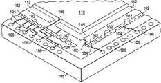
- semiconductor die 70has contact pads 72 formed on its active surface.
- RDLs 74electrically connect contact pads 72 to THVs 76 .
- some of the contact pads 72are electrically isolated from adjacent THVs 76 , i.e., no connecting RDL is formed.
- THVs 76are formed in molding compound 80 which operates as the die extension region as described in FIGS. 2 a - 2 e .
- molding compound 80is formed with sufficient width to contain THVs 76 (full vias) and THVs 82 (half vias).
- a ground plane or ring 84is formed on an active surface of semiconductor die 70 .
- a power ring 86is formed around ground plane or ring 84 on semiconductor die 36 .
- Ground plane or ring 84 and power ring 86can be made with Al, AlCu, Cu, or Cu alloy and deposited using an evaporation, electrolytic plating, electroless plating, or screen printing process.
- plane or ring 84is used for the power connection and ring 86 is used for the ground connection.
- a passivation layer 88is formed over RDLs 74 , contact pads 72 , power ring 86 , ground plane or ring 84 , and semiconductor die 70 for structural support and physical isolation. Passivation layer 88 can be made with SiO2, SiON, SixNy, PI, BCB, PBO, or other insulating material.
- RDLs 90are formed on a backside of the semiconductor die, opposite the active front side of the die, and electrically contact the backside of THVs 76 .
- RDLs 90can be made with Al, AlCu, Cu, or Cu alloy.
- a UBM 92is deposited and patterned to electrically contact RDLs 90 .
- UBMs 92may include a wetting layer, barrier layer, and adhesive layer.
- RDLs 90operate as an intermediate conduction layer to route electrical signals between THVs 76 and UBMs 92 .
- a passivation layer 94is formed over RDLs 90 , semiconductor die 70 , and molding compound 80 for structural support and physical isolation. Passivation layer 94 can be made with SiO2, SiON, SixNy, FI, BCB, PBO, or other insulating material.
- solder materialis deposited over UBMs 92 through an evaporation, electrolytic plating, electroless plating, ball drop, or screen printing process.
- the solder materialcan be any metal or electrically conductive material, e.g., Sn, Pb, Ni, Au, Ag, Cu, Bi and alloys thereof, or mixtures of other electrically conductive material.
- the solder materialis reflowed by heating the conductive material above its melting point to form spherical balls or bumps 96 .
- solder bumps 96are reflowed a second time to improve electrical contact to UBMs 92 .
- UBMs 92 and solder bumps 96represent one type of interconnect structure.
- Ground plane or ring 84connects through RDLs 74 to THVs 76 or 82 , which in turn connect through RDLs 90 and UBMs 92 to solder bumps 96 .
- power ring 86connects through RDLs 74 to THVs 76 or 82 , which in turn connect through RDLs 90 and UBMs 92 to solder bumps 96 .
- the wafer level ground plane or ring 84 and power ring 86provide shorter power and return path through THVs. The shorter path leads to less parasitic capacitance and enhanced electrical performance of the WLCSP package.
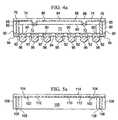
- semiconductor die 100has contact pads 102 formed on its active surface.
- RDLs 104electrically connect contact pads 102 to THVs 106 .
- some of the contact pads 102are electrically isolated from adjacent THVs 106 , i.e., no connecting RDL is formed.
- THVs 106are formed in molding compound 108 which operates as the die extension region as described in FIGS. 2 a - 2 d .
- molding compound 108is formed with sufficient width to contain THVs 106 (full vias).
- a ground plane or ring 110is formed on an active surface of semiconductor die 100 .
- a power ring 112is formed around ground plane or ring 110 on semiconductor die 100 .
- Ground plane or ring 110 and power ring 112can be made with Al, AlCu, Cu, or Cu alloy and deposited using an evaporation, electrolytic plating, electroless plating, or screen printing process.
- plane or ring 110is used for the power connection and ring 112 is used for the ground connection.
- a passivation layer 114is formed over RDLs 104 , contact pads 102 , power ring 112 , ground plane or ring 110 , and semiconductor die 100 for structural support and physical isolation.
- Passivation layer 114can be made with SiO2, SiON, SixNy, PI, BCB, PBO, or other insulating material.
- a plurality of semiconductor diecan be stacked and interconnected through THVs 106 , as shown in FIG. 5 c.
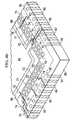
- semiconductor die 120has contact pads 122 formed on its active surface.
- RDLs 124electrically connect contact pads 122 to THVs 126 .
- some of the contact pads 122are electrically isolated from adjacent THVs 126 , i.e., no connecting RDL is formed.
- THVs 126are formed in molding compound 130 which operates as the die extension region as described in FIGS. 2 a - 2 e .
- molding compound 80is formed with sufficient width to contain THVs 126 (half vias) and other THVs (full vias).
- RDLs 140are formed on a backside of the semiconductor die, opposite the active front side of the die, and electrically contact the backside of THVs 126 .
- RDLs 140can be made with Al, AlCu, Cu, or Cu alloy.
- a UBM 142is deposited and patterned to electrically contact RDLs 140 .
- UBMs 142may include a wetting layer, barrier layer, and adhesive layer.
- RDLs 140operate as an intermediate conduction layer to route electrical signals between THVs 126 and UBMs 142 .
- a passivation layer 144is formed over RDLs 140 , semiconductor die 120 , and molding compound 130 for structural support and physical isolation. Passivation layer 144 can be made with SiO2, SiON, SixNy, PI, BCB, PBO, or other insulating material.
- solder materialis deposited over UBMs 142 through an evaporation, electrolytic plating, electroless plating, ball drop, or screen printing process.
- the solder materialcan be any metal or electrically conductive material, e.g., Sn, Pb, Ni, Au, Ag, Cu, Bi and alloys thereof, or mixtures of other electrically conductive material.
- the solder materialis reflowed by heating the conductive material above its melting point to form spherical balls or bumps 146 . In some applications, solder bumps 146 are reflowed a second time to improve electrical contact to UBMs 142 .
- UBMs 142 and solder bumps 146represent one type of interconnect structure.
- a ground plane or ring 150is formed over insulating layer 152 , which can be part of molding compound 130 or a passivation layer.
- a passivation layer 154is formed over RDL 124 .
- UBM 156connects to RDL 124 .
- Solder bump 158is formed on UBM 156 .
- UBM 164connects to ground plane or ring 150 .
- Solder bump 166is formed on UBM 164 . Solder bump 166 can also be used as a heat sink.
Landscapes
- Engineering & Computer Science (AREA)
- Microelectronics & Electronic Packaging (AREA)
- Computer Hardware Design (AREA)
- Power Engineering (AREA)
- Physics & Mathematics (AREA)
- Condensed Matter Physics & Semiconductors (AREA)
- General Physics & Mathematics (AREA)
- Manufacturing & Machinery (AREA)
- Geometry (AREA)
- Internal Circuitry In Semiconductor Integrated Circuit Devices (AREA)
- Semiconductor Integrated Circuits (AREA)
Abstract
Description
Claims (24)
Priority Applications (4)
| Application Number | Priority Date | Filing Date | Title |
|---|---|---|---|
| US11/951,729US7838395B2 (en) | 2007-12-06 | 2007-12-06 | Semiconductor wafer level interconnect package utilizing conductive ring and pad for separate voltage supplies and method of making the same |
| US12/905,797US8097943B2 (en) | 2007-12-06 | 2010-10-15 | Semiconductor device and method of forming wafer level ground plane and power ring |
| US13/346,415US9390991B2 (en) | 2007-12-06 | 2012-01-09 | Semiconductor device and method of forming wafer level ground plane and power ring |
| US15/177,081US10651139B2 (en) | 2007-12-06 | 2016-06-08 | Semiconductor device and method of forming wafer level ground plane and power ring |
Applications Claiming Priority (1)
| Application Number | Priority Date | Filing Date | Title |
|---|---|---|---|
| US11/951,729US7838395B2 (en) | 2007-12-06 | 2007-12-06 | Semiconductor wafer level interconnect package utilizing conductive ring and pad for separate voltage supplies and method of making the same |
Related Child Applications (1)
| Application Number | Title | Priority Date | Filing Date |
|---|---|---|---|
| US12/905,797ContinuationUS8097943B2 (en) | 2007-12-06 | 2010-10-15 | Semiconductor device and method of forming wafer level ground plane and power ring |
Publications (2)
| Publication Number | Publication Date |
|---|---|
| US20090146297A1 US20090146297A1 (en) | 2009-06-11 |
| US7838395B2true US7838395B2 (en) | 2010-11-23 |
Family
ID=40720785
Family Applications (4)
| Application Number | Title | Priority Date | Filing Date |
|---|---|---|---|
| US11/951,729Active2028-02-26US7838395B2 (en) | 2007-12-06 | 2007-12-06 | Semiconductor wafer level interconnect package utilizing conductive ring and pad for separate voltage supplies and method of making the same |
| US12/905,797ActiveUS8097943B2 (en) | 2007-12-06 | 2010-10-15 | Semiconductor device and method of forming wafer level ground plane and power ring |
| US13/346,415Active2029-10-01US9390991B2 (en) | 2007-12-06 | 2012-01-09 | Semiconductor device and method of forming wafer level ground plane and power ring |
| US15/177,081ActiveUS10651139B2 (en) | 2007-12-06 | 2016-06-08 | Semiconductor device and method of forming wafer level ground plane and power ring |
Family Applications After (3)
| Application Number | Title | Priority Date | Filing Date |
|---|---|---|---|
| US12/905,797ActiveUS8097943B2 (en) | 2007-12-06 | 2010-10-15 | Semiconductor device and method of forming wafer level ground plane and power ring |
| US13/346,415Active2029-10-01US9390991B2 (en) | 2007-12-06 | 2012-01-09 | Semiconductor device and method of forming wafer level ground plane and power ring |
| US15/177,081ActiveUS10651139B2 (en) | 2007-12-06 | 2016-06-08 | Semiconductor device and method of forming wafer level ground plane and power ring |
Country Status (1)
| Country | Link |
|---|---|
| US (4) | US7838395B2 (en) |
Cited By (12)
| Publication number | Priority date | Publication date | Assignee | Title |
|---|---|---|---|---|
| US20110309468A1 (en)* | 2010-06-17 | 2011-12-22 | Samsung Electronics Co., Ltd. | Semiconductor chip package and method of manufacturing the same |
| US8541991B2 (en) | 2008-04-16 | 2013-09-24 | Enpirion, Inc. | Power converter with controller operable in selected modes of operation |
| US8618900B2 (en) | 2007-09-10 | 2013-12-31 | Enpirion, Inc. | Micromagnetic device and method of forming the same |
| US8686698B2 (en) | 2008-04-16 | 2014-04-01 | Enpirion, Inc. | Power converter with controller operable in selected modes of operation |
| US8692532B2 (en) | 2008-04-16 | 2014-04-08 | Enpirion, Inc. | Power converter with controller operable in selected modes of operation |
| US8698463B2 (en) | 2008-12-29 | 2014-04-15 | Enpirion, Inc. | Power converter with a dynamically configurable controller based on a power conversion mode |
| US8867295B2 (en) | 2010-12-17 | 2014-10-21 | Enpirion, Inc. | Power converter for a memory module |
| US9246390B2 (en) | 2008-04-16 | 2016-01-26 | Enpirion, Inc. | Power converter with controller operable in selected modes of operation |
| US9509217B2 (en) | 2015-04-20 | 2016-11-29 | Altera Corporation | Asymmetric power flow controller for a power converter and method of operating the same |
| US9548714B2 (en) | 2008-12-29 | 2017-01-17 | Altera Corporation | Power converter with a dynamically configurable controller and output filter |
| US10651139B2 (en) | 2007-12-06 | 2020-05-12 | Jcet Semiconductor (Shaoxing) Co., Ltd. | Semiconductor device and method of forming wafer level ground plane and power ring |
| US20210210462A1 (en)* | 2020-01-06 | 2021-07-08 | Texas Instruments Incorporated | Chip scale package with redistribution layer interrupts |
Families Citing this family (62)
| Publication number | Priority date | Publication date | Assignee | Title |
|---|---|---|---|---|
| US7426780B2 (en) | 2004-11-10 | 2008-09-23 | Enpirion, Inc. | Method of manufacturing a power module |
| US7462317B2 (en)* | 2004-11-10 | 2008-12-09 | Enpirion, Inc. | Method of manufacturing an encapsulated package for a magnetic device |
| US8701272B2 (en) | 2005-10-05 | 2014-04-22 | Enpirion, Inc. | Method of forming a power module with a magnetic device having a conductive clip |
| US8631560B2 (en)* | 2005-10-05 | 2014-01-21 | Enpirion, Inc. | Method of forming a magnetic device having a conductive clip |
| US8139362B2 (en)* | 2005-10-05 | 2012-03-20 | Enpirion, Inc. | Power module with a magnetic device having a conductive clip |
| US7688172B2 (en) | 2005-10-05 | 2010-03-30 | Enpirion, Inc. | Magnetic device having a conductive clip |
| US8133529B2 (en)* | 2007-09-10 | 2012-03-13 | Enpirion, Inc. | Method of forming a micromagnetic device |
| US8018315B2 (en)* | 2007-09-10 | 2011-09-13 | Enpirion, Inc. | Power converter employing a micromagnetic device |
| US7955868B2 (en)* | 2007-09-10 | 2011-06-07 | Enpirion, Inc. | Method of forming a micromagnetic device |
| US7952459B2 (en)* | 2007-09-10 | 2011-05-31 | Enpirion, Inc. | Micromagnetic device and method of forming the same |
| TWI360207B (en) | 2007-10-22 | 2012-03-11 | Advanced Semiconductor Eng | Chip package structure and method of manufacturing |
| TWI453877B (en)* | 2008-11-07 | 2014-09-21 | Advanced Semiconductor Eng | Structure and process of embedded chip package |
| US9054086B2 (en) | 2008-10-02 | 2015-06-09 | Enpirion, Inc. | Module having a stacked passive element and method of forming the same |
| US8266793B2 (en)* | 2008-10-02 | 2012-09-18 | Enpirion, Inc. | Module having a stacked magnetic device and semiconductor device and method of forming the same |
| US8153473B2 (en)* | 2008-10-02 | 2012-04-10 | Empirion, Inc. | Module having a stacked passive element and method of forming the same |
| US8339802B2 (en)* | 2008-10-02 | 2012-12-25 | Enpirion, Inc. | Module having a stacked magnetic device and semiconductor device and method of forming the same |
| US8125072B2 (en)* | 2009-08-13 | 2012-02-28 | Infineon Technologies Ag | Device including a ring-shaped metal structure and method |
| US8536690B2 (en)* | 2009-09-22 | 2013-09-17 | Stats Chippac Ltd. | Integrated circuit packaging system with cap layer and method of manufacture thereof |
| TWI392069B (en)* | 2009-11-24 | 2013-04-01 | Advanced Semiconductor Eng | Package structure and packaging process thereof |
| US8435837B2 (en)* | 2009-12-15 | 2013-05-07 | Silicon Storage Technology, Inc. | Panel based lead frame packaging method and device |
| US8569894B2 (en) | 2010-01-13 | 2013-10-29 | Advanced Semiconductor Engineering, Inc. | Semiconductor package with single sided substrate design and manufacturing methods thereof |
| US8320134B2 (en) | 2010-02-05 | 2012-11-27 | Advanced Semiconductor Engineering, Inc. | Embedded component substrate and manufacturing methods thereof |
| TWI411075B (en) | 2010-03-22 | 2013-10-01 | Advanced Semiconductor Eng | Semiconductor package and manufacturing method thereof |
| TWI446420B (en) | 2010-08-27 | 2014-07-21 | Advanced Semiconductor Eng | Carrier separation method for semiconductor process |
| TWI445152B (en) | 2010-08-30 | 2014-07-11 | Advanced Semiconductor Eng | Semiconductor structure and method for manufacturing the same |
| US9007273B2 (en) | 2010-09-09 | 2015-04-14 | Advances Semiconductor Engineering, Inc. | Semiconductor package integrated with conformal shield and antenna |
| TWI434387B (en) | 2010-10-11 | 2014-04-11 | Advanced Semiconductor Eng | Semiconductor element having a via and package having a semiconductor element with a via and method for making the same |
| TWI527174B (en) | 2010-11-19 | 2016-03-21 | 日月光半導體製造股份有限公司 | Package having semiconductor device |
| US8368202B2 (en) | 2010-11-24 | 2013-02-05 | Advanced Semiconductor Engineering, Inc. | Semiconductor device and semiconductor package having the same |
| US9406658B2 (en) | 2010-12-17 | 2016-08-02 | Advanced Semiconductor Engineering, Inc. | Embedded component device and manufacturing methods thereof |
| TWI445155B (en) | 2011-01-06 | 2014-07-11 | Advanced Semiconductor Eng | Stacked semiconductor package and method for making the same |
| US8853819B2 (en) | 2011-01-07 | 2014-10-07 | Advanced Semiconductor Engineering, Inc. | Semiconductor structure with passive element network and manufacturing method thereof |
| US8487426B2 (en) | 2011-03-15 | 2013-07-16 | Advanced Semiconductor Engineering, Inc. | Semiconductor package with embedded die and manufacturing methods thereof |
| TWI421995B (en)* | 2011-04-27 | 2014-01-01 | Unimicron Technology Corp | Semiconductor package structure and fabrication method thereof |
| US8541883B2 (en) | 2011-11-29 | 2013-09-24 | Advanced Semiconductor Engineering, Inc. | Semiconductor device having shielded conductive vias |
| US8796139B2 (en)* | 2011-12-29 | 2014-08-05 | Stmicroelectronics Pte Ltd | Embedded wafer level ball grid array bar systems and methods |
| US8975157B2 (en) | 2012-02-08 | 2015-03-10 | Advanced Semiconductor Engineering, Inc. | Carrier bonding and detaching processes for a semiconductor wafer |
| US8963316B2 (en) | 2012-02-15 | 2015-02-24 | Advanced Semiconductor Engineering, Inc. | Semiconductor device and method for manufacturing the same |
| EP2648218B1 (en)* | 2012-04-05 | 2015-10-14 | Nxp B.V. | Integrated circuit and method of manufacturing the same |
| US8786060B2 (en) | 2012-05-04 | 2014-07-22 | Advanced Semiconductor Engineering, Inc. | Semiconductor package integrated with conformal shield and antenna |
| TWI496261B (en)* | 2012-07-05 | 2015-08-11 | Unimicron Technology Corp | Electical device package structure and method of fabricating the same |
| CN103545225B (en)* | 2012-07-13 | 2016-12-21 | 欣兴电子股份有限公司 | Electronic component packaging structure and packaging method |
| US9153542B2 (en) | 2012-08-01 | 2015-10-06 | Advanced Semiconductor Engineering, Inc. | Semiconductor package having an antenna and manufacturing method thereof |
| US8937387B2 (en) | 2012-11-07 | 2015-01-20 | Advanced Semiconductor Engineering, Inc. | Semiconductor device with conductive vias |
| US8952542B2 (en) | 2012-11-14 | 2015-02-10 | Advanced Semiconductor Engineering, Inc. | Method for dicing a semiconductor wafer having through silicon vias and resultant structures |
| US9406552B2 (en) | 2012-12-20 | 2016-08-02 | Advanced Semiconductor Engineering, Inc. | Semiconductor device having conductive via and manufacturing process |
| US9161454B2 (en) | 2012-12-24 | 2015-10-13 | Unimicron Technology Corp. | Electrical device package structure and method of fabricating the same |
| US8841751B2 (en) | 2013-01-23 | 2014-09-23 | Advanced Semiconductor Engineering, Inc. | Through silicon vias for semiconductor devices and manufacturing method thereof |
| US9488862B2 (en)* | 2013-02-12 | 2016-11-08 | Apple Inc. | Displays with organic light-emitting diode backlight structures |
| US9978688B2 (en) | 2013-02-28 | 2018-05-22 | Advanced Semiconductor Engineering, Inc. | Semiconductor package having a waveguide antenna and manufacturing method thereof |
| US9685350B2 (en) | 2013-03-08 | 2017-06-20 | STATS ChipPAC, Pte. Ltd. | Semiconductor device and method of forming embedded conductive layer for power/ground planes in Fo-eWLB |
| US9089268B2 (en) | 2013-03-13 | 2015-07-28 | Advanced Semiconductor Engineering, Inc. | Neural sensing device and method for making the same |
| US8987734B2 (en) | 2013-03-15 | 2015-03-24 | Advanced Semiconductor Engineering, Inc. | Semiconductor wafer, semiconductor process and semiconductor package |
| US9173583B2 (en) | 2013-03-15 | 2015-11-03 | Advanced Semiconductor Engineering, Inc. | Neural sensing device and method for making the same |
| US9543373B2 (en)* | 2013-10-23 | 2017-01-10 | Taiwan Semiconductor Manufacturing Company, Ltd. | Semiconductor structure and manufacturing method thereof |
| CN104952810B (en)* | 2014-03-26 | 2019-05-21 | 中芯国际集成电路制造(上海)有限公司 | A kind of bonded wafers and preparation method thereof |
| US9786631B2 (en)* | 2014-11-26 | 2017-10-10 | Taiwan Semiconductor Manufacturing Company, Ltd. | Device package with reduced thickness and method for forming same |
| US9691694B2 (en) | 2015-02-18 | 2017-06-27 | Qualcomm Incorporated | Substrate comprising stacks of interconnects, interconnect on solder resist layer and interconnect on side portion of substrate |
| KR20170001060A (en)* | 2015-06-25 | 2017-01-04 | 에스케이하이닉스 주식회사 | Semiconductor package including interposer and manufacturing method for the same |
| US10825821B2 (en) | 2015-12-18 | 2020-11-03 | International Business Machines Corporation | Cooling and power delivery for a wafer level computing board |
| US9704830B1 (en) | 2016-01-13 | 2017-07-11 | International Business Machines Corporation | Semiconductor structure and method of making |
| CN107180879A (en)* | 2017-04-13 | 2017-09-19 | 深圳市速腾聚创科技有限公司 | Photodiode packaging device |
Citations (7)
| Publication number | Priority date | Publication date | Assignee | Title |
|---|---|---|---|---|
| US6181569B1 (en) | 1999-06-07 | 2001-01-30 | Kishore K. Chakravorty | Low cost chip size package and method of fabricating the same |
| US6368896B2 (en) | 1997-10-31 | 2002-04-09 | Micron Technology, Inc. | Method of wafer level chip scale packaging |
| US6492719B2 (en)* | 1999-07-30 | 2002-12-10 | Hitachi, Ltd. | Semiconductor device |
| US6608377B2 (en) | 2001-01-30 | 2003-08-19 | Samsung Electronics Co., Ltd. | Wafer level package including ground metal layer |
| JP2004214501A (en) | 2003-01-07 | 2004-07-29 | Sony Corp | Wafer level chip size package and its manufacturing method |
| US20060197234A1 (en)* | 2005-02-25 | 2006-09-07 | Heinz Pape | Semiconductor device including a semiconductor chip with signal contact areas and supply contact areas, and method for producing the semiconductor device |
| US20090008793A1 (en)* | 2007-07-02 | 2009-01-08 | Infineon Technologies Ag | Semiconductor device |
Family Cites Families (6)
| Publication number | Priority date | Publication date | Assignee | Title |
|---|---|---|---|---|
| TW533517B (en)* | 2002-02-26 | 2003-05-21 | Silicon Integrated Sys Corp | Substrate for semiconductor package |
| EP1654765A2 (en)* | 2004-01-10 | 2006-05-10 | Hvvi Semiconductors, Inc. | Power semiconductor device and method therefor cross reference to related applications |
| JP3998647B2 (en)* | 2004-02-12 | 2007-10-31 | 株式会社東芝 | Semiconductor chip and method for testing semiconductor chip |
| US9129826B2 (en)* | 2005-05-31 | 2015-09-08 | Stats Chippac Ltd. | Epoxy bump for overhang die |
| KR100719376B1 (en)* | 2006-01-05 | 2007-05-17 | 삼성전자주식회사 | Semiconductor device having pad structure capable of reducing failures of mounting process |
| US7838395B2 (en) | 2007-12-06 | 2010-11-23 | Stats Chippac, Ltd. | Semiconductor wafer level interconnect package utilizing conductive ring and pad for separate voltage supplies and method of making the same |
- 2007
- 2007-12-06USUS11/951,729patent/US7838395B2/enactiveActive
- 2010
- 2010-10-15USUS12/905,797patent/US8097943B2/enactiveActive
- 2012
- 2012-01-09USUS13/346,415patent/US9390991B2/enactiveActive
- 2016
- 2016-06-08USUS15/177,081patent/US10651139B2/enactiveActive
Patent Citations (7)
| Publication number | Priority date | Publication date | Assignee | Title |
|---|---|---|---|---|
| US6368896B2 (en) | 1997-10-31 | 2002-04-09 | Micron Technology, Inc. | Method of wafer level chip scale packaging |
| US6181569B1 (en) | 1999-06-07 | 2001-01-30 | Kishore K. Chakravorty | Low cost chip size package and method of fabricating the same |
| US6492719B2 (en)* | 1999-07-30 | 2002-12-10 | Hitachi, Ltd. | Semiconductor device |
| US6608377B2 (en) | 2001-01-30 | 2003-08-19 | Samsung Electronics Co., Ltd. | Wafer level package including ground metal layer |
| JP2004214501A (en) | 2003-01-07 | 2004-07-29 | Sony Corp | Wafer level chip size package and its manufacturing method |
| US20060197234A1 (en)* | 2005-02-25 | 2006-09-07 | Heinz Pape | Semiconductor device including a semiconductor chip with signal contact areas and supply contact areas, and method for producing the semiconductor device |
| US20090008793A1 (en)* | 2007-07-02 | 2009-01-08 | Infineon Technologies Ag | Semiconductor device |
Cited By (15)
| Publication number | Priority date | Publication date | Assignee | Title |
|---|---|---|---|---|
| US8618900B2 (en) | 2007-09-10 | 2013-12-31 | Enpirion, Inc. | Micromagnetic device and method of forming the same |
| US9299489B2 (en) | 2007-09-10 | 2016-03-29 | Enpirion, Inc. | Micromagnetic device and method of forming the same |
| US10651139B2 (en) | 2007-12-06 | 2020-05-12 | Jcet Semiconductor (Shaoxing) Co., Ltd. | Semiconductor device and method of forming wafer level ground plane and power ring |
| US8541991B2 (en) | 2008-04-16 | 2013-09-24 | Enpirion, Inc. | Power converter with controller operable in selected modes of operation |
| US8686698B2 (en) | 2008-04-16 | 2014-04-01 | Enpirion, Inc. | Power converter with controller operable in selected modes of operation |
| US8692532B2 (en) | 2008-04-16 | 2014-04-08 | Enpirion, Inc. | Power converter with controller operable in selected modes of operation |
| US9246390B2 (en) | 2008-04-16 | 2016-01-26 | Enpirion, Inc. | Power converter with controller operable in selected modes of operation |
| US9548714B2 (en) | 2008-12-29 | 2017-01-17 | Altera Corporation | Power converter with a dynamically configurable controller and output filter |
| US8698463B2 (en) | 2008-12-29 | 2014-04-15 | Enpirion, Inc. | Power converter with a dynamically configurable controller based on a power conversion mode |
| US20110309468A1 (en)* | 2010-06-17 | 2011-12-22 | Samsung Electronics Co., Ltd. | Semiconductor chip package and method of manufacturing the same |
| US8867295B2 (en) | 2010-12-17 | 2014-10-21 | Enpirion, Inc. | Power converter for a memory module |
| US9627028B2 (en) | 2010-12-17 | 2017-04-18 | Enpirion, Inc. | Power converter for a memory module |
| US10084380B2 (en) | 2015-04-20 | 2018-09-25 | Altera Corporation | Asymmetric power flow controller for a power converter and method of operating the same |
| US9509217B2 (en) | 2015-04-20 | 2016-11-29 | Altera Corporation | Asymmetric power flow controller for a power converter and method of operating the same |
| US20210210462A1 (en)* | 2020-01-06 | 2021-07-08 | Texas Instruments Incorporated | Chip scale package with redistribution layer interrupts |
Also Published As
| Publication number | Publication date |
|---|---|
| US20090146297A1 (en) | 2009-06-11 |
| US8097943B2 (en) | 2012-01-17 |
| US10651139B2 (en) | 2020-05-12 |
| US20110024903A1 (en) | 2011-02-03 |
| US20120104601A1 (en) | 2012-05-03 |
| US20160293558A1 (en) | 2016-10-06 |
| US9390991B2 (en) | 2016-07-12 |
Similar Documents
| Publication | Publication Date | Title |
|---|---|---|
| US10651139B2 (en) | Semiconductor device and method of forming wafer level ground plane and power ring | |
| US8592252B2 (en) | Semiconductor device and method of forming through hole vias in die extension region around periphery of die | |
| US8241954B2 (en) | Wafer level die integration and method | |
| US10074553B2 (en) | Wafer level package integration and method | |
| US8039960B2 (en) | Solder bump with inner core pillar in semiconductor package | |
| US7842607B2 (en) | Semiconductor device and method of providing a thermal dissipation path through RDL and conductive via | |
| US7667335B2 (en) | Semiconductor package with passivation island for reducing stress on solder bumps | |
| US8017515B2 (en) | Semiconductor device and method of forming compliant polymer layer between UBM and conformal dielectric layer/RDL for stress relief | |
| US8921983B2 (en) | Semiconductor package and method of forming similar structure for top and bottom bonding pads | |
| KR20090031650A (en) | Semiconductor package and method for reducing electromagnetic interference between devices | |
| US20120018874A1 (en) | Semiconductor Device and Method of Forming RDL over Contact Pad with High Alignment Tolerance or Reduced Interconnect Pitch | |
| US9466577B2 (en) | Semiconductor interconnect structure with stacked vias separated by signal line and method therefor |
Legal Events
| Date | Code | Title | Description |
|---|---|---|---|
| AS | Assignment | Owner name:STATS CHIPPAC, LTD., SINGAPORE Free format text:ASSIGNMENT OF ASSIGNORS INTEREST;ASSIGNORS:BADAKERE, GURUPRASAD G.;CAMACHO, ZIGMUND R.;TAY, LIONEL CHIEN HUI;REEL/FRAME:020212/0528 Effective date:20071207 | |
| STCF | Information on status: patent grant | Free format text:PATENTED CASE | |
| FPAY | Fee payment | Year of fee payment:4 | |
| AS | Assignment | Owner name:CITICORP INTERNATIONAL LIMITED, AS COMMON SECURITY AGENT, HONG KONG Free format text:SECURITY INTEREST;ASSIGNORS:STATS CHIPPAC, INC.;STATS CHIPPAC LTD.;REEL/FRAME:036288/0748 Effective date:20150806 Owner name:CITICORP INTERNATIONAL LIMITED, AS COMMON SECURITY Free format text:SECURITY INTEREST;ASSIGNORS:STATS CHIPPAC, INC.;STATS CHIPPAC LTD.;REEL/FRAME:036288/0748 Effective date:20150806 | |
| AS | Assignment | Owner name:STATS CHIPPAC PTE. LTE., SINGAPORE Free format text:CHANGE OF NAME;ASSIGNOR:STATS CHIPPAC LTD.;REEL/FRAME:038378/0309 Effective date:20160329 | |
| MAFP | Maintenance fee payment | Free format text:PAYMENT OF MAINTENANCE FEE, 8TH YEAR, LARGE ENTITY (ORIGINAL EVENT CODE: M1552) Year of fee payment:8 | |
| AS | Assignment | Owner name:STATS CHIPPAC PTE. LTD. FORMERLY KNOWN AS STATS CH Free format text:RELEASE BY SECURED PARTY;ASSIGNOR:CITICORP INTERNATIONAL LIMITED, AS COMMON SECURITY AGENT;REEL/FRAME:051285/0318 Effective date:20190503 Owner name:STATS CHIPPAC, INC., CALIFORNIA Free format text:RELEASE BY SECURED PARTY;ASSIGNOR:CITICORP INTERNATIONAL LIMITED, AS COMMON SECURITY AGENT;REEL/FRAME:051285/0318 Effective date:20190503 Owner name:STATS CHIPPAC PTE. LTD. FORMERLY KNOWN AS STATS CHIPPAC LTD., SINGAPORE Free format text:RELEASE BY SECURED PARTY;ASSIGNOR:CITICORP INTERNATIONAL LIMITED, AS COMMON SECURITY AGENT;REEL/FRAME:051285/0318 Effective date:20190503 | |
| AS | Assignment | Owner name:JCET SEMICONDUCTOR (SHAOXING) CO., LTD., CHINA Free format text:ASSIGNMENT OF ASSIGNORS INTEREST;ASSIGNOR:STATS CHIPPAC PTE. LTD.;REEL/FRAME:051365/0680 Effective date:20191128 | |
| MAFP | Maintenance fee payment | Free format text:PAYMENT OF MAINTENANCE FEE, 12TH YEAR, LARGE ENTITY (ORIGINAL EVENT CODE: M1553); ENTITY STATUS OF PATENT OWNER: LARGE ENTITY Year of fee payment:12 | |
| AS | Assignment | Owner name:STATS CHIPPAC PTE. LTD., SINGAPORE Free format text:CORRECTIVE ASSIGNMENT TO CORRECT THE THE ASSIGNEE'S NAME PREVIOUSLY RECORDED AT REEL: 038378 FRAME: 0309. ASSIGNOR(S) HEREBY CONFIRMS THE ASSIGNMENT;ASSIGNOR:STATS CHIPPAC LTD.;REEL/FRAME:065236/0767 Effective date:20160329 |