US7838133B2 - Deposition of perovskite and other compound ceramic films for dielectric applications - Google Patents
Deposition of perovskite and other compound ceramic films for dielectric applicationsDownload PDFInfo
- Publication number
- US7838133B2 US7838133B2US11/218,652US21865205AUS7838133B2US 7838133 B2US7838133 B2US 7838133B2US 21865205 AUS21865205 AUS 21865205AUS 7838133 B2US7838133 B2US 7838133B2
- Authority
- US
- United States
- Prior art keywords
- substrate
- perovskite
- crystalline
- layer
- target
- Prior art date
- Legal status (The legal status is an assumption and is not a legal conclusion. Google has not performed a legal analysis and makes no representation as to the accuracy of the status listed.)
- Expired - Fee Related, expires
Links
Images


Classifications
- H—ELECTRICITY
- H01—ELECTRIC ELEMENTS
- H01L—SEMICONDUCTOR DEVICES NOT COVERED BY CLASS H10
- H01L21/00—Processes or apparatus adapted for the manufacture or treatment of semiconductor or solid state devices or of parts thereof
- H01L21/02—Manufacture or treatment of semiconductor devices or of parts thereof
- H01L21/02104—Forming layers
- H01L21/02107—Forming insulating materials on a substrate
- H01L21/02109—Forming insulating materials on a substrate characterised by the type of layer, e.g. type of material, porous/non-porous, pre-cursors, mixtures or laminates
- H01L21/02112—Forming insulating materials on a substrate characterised by the type of layer, e.g. type of material, porous/non-porous, pre-cursors, mixtures or laminates characterised by the material of the layer
- H01L21/02172—Forming insulating materials on a substrate characterised by the type of layer, e.g. type of material, porous/non-porous, pre-cursors, mixtures or laminates characterised by the material of the layer the material containing at least one metal element, e.g. metal oxides, metal nitrides, metal oxynitrides or metal carbides
- H01L21/02197—Forming insulating materials on a substrate characterised by the type of layer, e.g. type of material, porous/non-porous, pre-cursors, mixtures or laminates characterised by the material of the layer the material containing at least one metal element, e.g. metal oxides, metal nitrides, metal oxynitrides or metal carbides the material having a perovskite structure, e.g. BaTiO3
- C—CHEMISTRY; METALLURGY
- C23—COATING METALLIC MATERIAL; COATING MATERIAL WITH METALLIC MATERIAL; CHEMICAL SURFACE TREATMENT; DIFFUSION TREATMENT OF METALLIC MATERIAL; COATING BY VACUUM EVAPORATION, BY SPUTTERING, BY ION IMPLANTATION OR BY CHEMICAL VAPOUR DEPOSITION, IN GENERAL; INHIBITING CORROSION OF METALLIC MATERIAL OR INCRUSTATION IN GENERAL
- C23C—COATING METALLIC MATERIAL; COATING MATERIAL WITH METALLIC MATERIAL; SURFACE TREATMENT OF METALLIC MATERIAL BY DIFFUSION INTO THE SURFACE, BY CHEMICAL CONVERSION OR SUBSTITUTION; COATING BY VACUUM EVAPORATION, BY SPUTTERING, BY ION IMPLANTATION OR BY CHEMICAL VAPOUR DEPOSITION, IN GENERAL
- C23C14/00—Coating by vacuum evaporation, by sputtering or by ion implantation of the coating forming material
- C23C14/06—Coating by vacuum evaporation, by sputtering or by ion implantation of the coating forming material characterised by the coating material
- C23C14/08—Oxides
- C23C14/088—Oxides of the type ABO3 with A representing alkali, alkaline earth metal or Pb and B representing a refractory or rare earth metal
- C—CHEMISTRY; METALLURGY
- C23—COATING METALLIC MATERIAL; COATING MATERIAL WITH METALLIC MATERIAL; CHEMICAL SURFACE TREATMENT; DIFFUSION TREATMENT OF METALLIC MATERIAL; COATING BY VACUUM EVAPORATION, BY SPUTTERING, BY ION IMPLANTATION OR BY CHEMICAL VAPOUR DEPOSITION, IN GENERAL; INHIBITING CORROSION OF METALLIC MATERIAL OR INCRUSTATION IN GENERAL
- C23C—COATING METALLIC MATERIAL; COATING MATERIAL WITH METALLIC MATERIAL; SURFACE TREATMENT OF METALLIC MATERIAL BY DIFFUSION INTO THE SURFACE, BY CHEMICAL CONVERSION OR SUBSTITUTION; COATING BY VACUUM EVAPORATION, BY SPUTTERING, BY ION IMPLANTATION OR BY CHEMICAL VAPOUR DEPOSITION, IN GENERAL
- C23C14/00—Coating by vacuum evaporation, by sputtering or by ion implantation of the coating forming material
- C23C14/22—Coating by vacuum evaporation, by sputtering or by ion implantation of the coating forming material characterised by the process of coating
- C23C14/34—Sputtering
- C23C14/3407—Cathode assembly for sputtering apparatus, e.g. Target
- C23C14/3414—Metallurgical or chemical aspects of target preparation, e.g. casting, powder metallurgy
- C—CHEMISTRY; METALLURGY
- C23—COATING METALLIC MATERIAL; COATING MATERIAL WITH METALLIC MATERIAL; CHEMICAL SURFACE TREATMENT; DIFFUSION TREATMENT OF METALLIC MATERIAL; COATING BY VACUUM EVAPORATION, BY SPUTTERING, BY ION IMPLANTATION OR BY CHEMICAL VAPOUR DEPOSITION, IN GENERAL; INHIBITING CORROSION OF METALLIC MATERIAL OR INCRUSTATION IN GENERAL
- C23C—COATING METALLIC MATERIAL; COATING MATERIAL WITH METALLIC MATERIAL; SURFACE TREATMENT OF METALLIC MATERIAL BY DIFFUSION INTO THE SURFACE, BY CHEMICAL CONVERSION OR SUBSTITUTION; COATING BY VACUUM EVAPORATION, BY SPUTTERING, BY ION IMPLANTATION OR BY CHEMICAL VAPOUR DEPOSITION, IN GENERAL
- C23C14/00—Coating by vacuum evaporation, by sputtering or by ion implantation of the coating forming material
- C23C14/22—Coating by vacuum evaporation, by sputtering or by ion implantation of the coating forming material characterised by the process of coating
- C23C14/34—Sputtering
- C23C14/3435—Applying energy to the substrate during sputtering
- C23C14/345—Applying energy to the substrate during sputtering using substrate bias
- C—CHEMISTRY; METALLURGY
- C23—COATING METALLIC MATERIAL; COATING MATERIAL WITH METALLIC MATERIAL; CHEMICAL SURFACE TREATMENT; DIFFUSION TREATMENT OF METALLIC MATERIAL; COATING BY VACUUM EVAPORATION, BY SPUTTERING, BY ION IMPLANTATION OR BY CHEMICAL VAPOUR DEPOSITION, IN GENERAL; INHIBITING CORROSION OF METALLIC MATERIAL OR INCRUSTATION IN GENERAL
- C23C—COATING METALLIC MATERIAL; COATING MATERIAL WITH METALLIC MATERIAL; SURFACE TREATMENT OF METALLIC MATERIAL BY DIFFUSION INTO THE SURFACE, BY CHEMICAL CONVERSION OR SUBSTITUTION; COATING BY VACUUM EVAPORATION, BY SPUTTERING, BY ION IMPLANTATION OR BY CHEMICAL VAPOUR DEPOSITION, IN GENERAL
- C23C14/00—Coating by vacuum evaporation, by sputtering or by ion implantation of the coating forming material
- C23C14/22—Coating by vacuum evaporation, by sputtering or by ion implantation of the coating forming material characterised by the process of coating
- C23C14/50—Substrate holders
- H—ELECTRICITY
- H01—ELECTRIC ELEMENTS
- H01G—CAPACITORS; CAPACITORS, RECTIFIERS, DETECTORS, SWITCHING DEVICES, LIGHT-SENSITIVE OR TEMPERATURE-SENSITIVE DEVICES OF THE ELECTROLYTIC TYPE
- H01G4/00—Fixed capacitors; Processes of their manufacture
- H01G4/002—Details
- H01G4/018—Dielectrics
- H01G4/06—Solid dielectrics
- H01G4/08—Inorganic dielectrics
- H01G4/085—Vapour deposited
- H—ELECTRICITY
- H01—ELECTRIC ELEMENTS
- H01G—CAPACITORS; CAPACITORS, RECTIFIERS, DETECTORS, SWITCHING DEVICES, LIGHT-SENSITIVE OR TEMPERATURE-SENSITIVE DEVICES OF THE ELECTROLYTIC TYPE
- H01G4/00—Fixed capacitors; Processes of their manufacture
- H01G4/002—Details
- H01G4/018—Dielectrics
- H01G4/06—Solid dielectrics
- H01G4/08—Inorganic dielectrics
- H01G4/12—Ceramic dielectrics
- H01G4/1209—Ceramic dielectrics characterised by the ceramic dielectric material
- H01G4/1218—Ceramic dielectrics characterised by the ceramic dielectric material based on titanium oxides or titanates
- H01G4/1227—Ceramic dielectrics characterised by the ceramic dielectric material based on titanium oxides or titanates based on alkaline earth titanates
- H—ELECTRICITY
- H01—ELECTRIC ELEMENTS
- H01G—CAPACITORS; CAPACITORS, RECTIFIERS, DETECTORS, SWITCHING DEVICES, LIGHT-SENSITIVE OR TEMPERATURE-SENSITIVE DEVICES OF THE ELECTROLYTIC TYPE
- H01G4/00—Fixed capacitors; Processes of their manufacture
- H01G4/30—Stacked capacitors
- H—ELECTRICITY
- H01—ELECTRIC ELEMENTS
- H01G—CAPACITORS; CAPACITORS, RECTIFIERS, DETECTORS, SWITCHING DEVICES, LIGHT-SENSITIVE OR TEMPERATURE-SENSITIVE DEVICES OF THE ELECTROLYTIC TYPE
- H01G4/00—Fixed capacitors; Processes of their manufacture
- H01G4/33—Thin- or thick-film capacitors (thin- or thick-film circuits; capacitors without a potential-jump or surface barrier specially adapted for integrated circuits, details thereof, multistep manufacturing processes therefor)
- H—ELECTRICITY
- H01—ELECTRIC ELEMENTS
- H01L—SEMICONDUCTOR DEVICES NOT COVERED BY CLASS H10
- H01L21/00—Processes or apparatus adapted for the manufacture or treatment of semiconductor or solid state devices or of parts thereof
- H01L21/02—Manufacture or treatment of semiconductor devices or of parts thereof
- H01L21/02104—Forming layers
- H01L21/02107—Forming insulating materials on a substrate
- H01L21/02225—Forming insulating materials on a substrate characterised by the process for the formation of the insulating layer
- H01L21/0226—Forming insulating materials on a substrate characterised by the process for the formation of the insulating layer formation by a deposition process
- H01L21/02263—Forming insulating materials on a substrate characterised by the process for the formation of the insulating layer formation by a deposition process deposition from the gas or vapour phase
- H01L21/02266—Forming insulating materials on a substrate characterised by the process for the formation of the insulating layer formation by a deposition process deposition from the gas or vapour phase deposition by physical ablation of a target, e.g. sputtering, reactive sputtering, physical vapour deposition or pulsed laser deposition
Definitions
- the present inventionis related to production and application of dielectric thin-films and, in particular, the deposition of perovskites such as Barium Strontium Titanate (BST) films and other ceramic oxides for dielectric applications.
- perovskitessuch as Barium Strontium Titanate (BST) films and other ceramic oxides for dielectric applications.
- Perovskite filmsfor example Barium Strontium Titanate (BST) films
- BSTBarium Strontium Titanate
- Perovskite filmsare one of the attractive materials to use in capacitors for high density device applications because of its relatively high dielectric constant, low leakage current density, high dielectric breakdown strength, and ferroelectric perovskite phase that does not exhibit fatigue.
- electric properties of the perovskite filmsare greatly dependent on the deposition process, the substrate, the post-processing, and the related film structure.
- thin film perovskiteshave rarely been utilized in manufacture primarily because of difficulties in controlling physical and chemical properties of the crystalline and amorphous phases of perovskite thin-film materials and their interactions with metallic and conductive electrodes.
- Solid-state thin-film devicesare typically formed by stacking thin films of metal and dielectric on a substrate.
- the thin filmstypically include two metallic electrodes with a dielectric layer in between.
- the thin filmscan be deposited utilizing a number of deposition processes, including sputtering, electroplating, chemical vapor deposition, sol gel, or oxidation.
- Substrates suitable for these applicationshave conventionally been high temperature materials capable of withstanding at least one high temperature anneal process to at least 650-750° C. so as to crystallize the perovskite dielectric film in order to increase its dielectric constant.
- Such a substratecan be any suitable material with appropriate structural and material properties, for example a semiconductor wafer, refractory metallic sheet (e.g., titanium, zirconium, or stainless steel), ceramic such as alumina, or other material capable of withstanding subsequent high temperature processing.
- a semiconductor wafere.g., silicon, zirconium, or stainless steel
- ceramice.g., alumina, or other material capable of withstanding subsequent high temperature processing.
- the dielectric materialis deposited in amorphous form and then the material is heated in an anneal process to form the crystalline material.
- Conventional formation of perovskite layersrequire an anneal at or above 650° C. to transform the deposited amorphous film to a crystalline form.
- Such a high temperature annealseverely limits the materials that can be utilized as the substrate, and often requires the use of expensive noble metals such as platinum to protect the substrate from reaction with the electrode material.
- Such high heat-treat temperaturesare incompatible with standard semiconductor or MEM device processing, and limit the choice of substrate materials on which the layers can be formed, increasing the cost, and decreasing the yield of such devices formed with the layers.
- the depositioncan provide a low-temperature, high deposition-rate deposition of a dense amorphous layer of BST from a conductive BST target, which can be annealed at much lower temperature to yield crystalline BST.
- Some embodiments of the depositionaddress the need for low temperature, high rate deposition of perovskite films, for example BST films, which can be utilized as the dielectric layer in high specific capacitance devices as, for example, de-coupling capacitors, energy storage devices, voltage tunable capacitors, or other micro-electronic devices.
- a method of depositing a perovskite or ceramic oxide layerincludes placing a substrate in a reactor; flowing a gaseous mixture, for example argon and oxygen, through the reactor; and applying pulsed-DC power to a target formed of conductive perovskite or ceramic oxide material, such as BST, positioned opposite the substrate.
- a gaseous mixturefor example argon and oxygen
- the perovskite layercan be formed utilizing radio frequency (RF) sputtering.
- the perovskiteis deposited by RF sputtering of a wide area target in the presence of a sputtering gas under a condition of uniform target erosion.
- the substrateis positioned opposite a planar target formed of perovskite, for example BST, the area of the target being larger than the area of the substrate.
- a central area of the target of the same size as the substrate and overlying the substrateis exposed to a uniform plasma condition, which provides a condition of uniform target erosion.
- a uniform plasma conditioncan be created without magnetic enhancement, termed diode sputtering, or by providing a time-averaged uniform magnetic field by scanning a magnet across the target in a plane parallel to the plane of the target.
- a film produced utilizing a pulsed dc, bias PVD process with a conductive ceramic targetcan be deposited at much higher rates than an insulating ceramic process, which requires an RF sputtering process. Further, deposition occurs with much less oxygen present in the gas flow to provide a fully oxidized film as opposed to a metallic target. The resulting film is much higher density than the low rate films.
- the filmscan be stoichiometric, uniform, highly dense, with low sintering temperatures and resulting high dielectric properties.
- the substrateis preheated.
- the substratecan be heated to a temperature of about 400° C. or below during deposition for low temperature perovskite deposition, or to higher temperatures for perovskite deposition on substrates capable of withstanding such temperature regime.
- Substrates suitable for low temperature perovskite depositioninclude glass, plastic, metal foil, stainless steel, and copper.
- a perovskite layer of thickness up to several microns thickcan be deposited, although layers of any thickness can be formed.
- the perovskite layer formed on the substrateis later annealed.
- the anneal temperaturecan be as low as 400° C. for low temperature anneal, and higher for perovskite deposition on substrates capable of withstanding such higher temperature regime.
- the perovskite targetcan be doped with transition metal dopants, for example manganese, transition elements, lanthanides (including the rare earth ions) and/or amphoteric elements.
- a stacked capacitor structurecan be formed.
- the stacked capacitor structureincludes one or more capacitor stacks deposited on a thin substrate, wherein each capacitor stack includes: a bottom electrode layer, a perovskite, for example BST, dielectric layer deposited over the bottom electrode layer; and a top electrode layer deposited over the dielectric layer.
- a top conducting layercan be deposited over the capacitor stacks.
- a capacitor structurecan be formed in a cluster tool.
- An exemplary method of producing a capacitor in a cluster toolincludes loading a substrate into the cluster tool; depositing an electrode layer over the substrate in a first chamber of the cluster tool; depositing a perovskite dielectric layer over the electrode layer in a second chamber of the cluster tool; depositing a second electrode layer over the dielectric layer in a third chamber.
- the first and the second electrode layerscan be deposited in the same chamber.
- a fixture for holding a thin substratecan include a top portion; and a bottom portion, wherein the thin substrate is held when the top portion is attached to the bottom portion.
- the ceramic layercan be deposited on a substrate coated with iridium or other refractory conductive material to provide a low temperature anneal processed capacitive structure.
- FIGS. 1A and 1Billustrate a pulsed-DC biased reactive deposition apparatus that can be utilized in the methods of depositing according to the present invention.
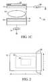
- FIG. 1Cillustrates an RF sputtering deposition apparatus.
- FIG. 2shows an example of a target that can be utilized in the reactor illustrated in FIGS. 1A , 1 B, and 1 C.
- FIGS. 3A and 3Billustrate a thin-film capacitor design according to some embodiments of the present invention.
- FIGS. 4A , 4 B, 4 C, and 4 Dillustrate a thin substrate mount and mask arrangement that can be utilized in the deposition of dielectric perovskite layers, for example BST films, deposited according to some embodiments of the present invention.
- FIG. 5illustrates a cluster tool that can be utilized to form batteries with dielectric perovskite layers deposited according to some embodiments of the present invention.
- FIG. 6illustrates an example of stacked capacitor structure with dielectric perovskite layers deposited according to some embodiments of the present invention.
- dielectric perovskite films or other ceramic oxide filmsare deposited on a substrate by a pulsed-DC physical vapor deposition (PVD) process utilizing a conductive ceramic target.
- PVDpulsed-DC physical vapor deposition
- the filmcan be deposited by RF sputtering.
- a dielectric perovskite layerfor example BST material
- BST materialis deposited directly on the substrate with only low temperature anneal, eliminating the need of a subsequent high temperature anneal to crystallize the film. Removing the high temperature anneal allows for formation of capacitor structures on light-weight, low temperature, and low cost substrates such as copper foil and plastic sheet, reducing both the weight and the cost of capacitors while maintaining the high dielectric constant of the perovskite, for example BST, high-density dielectric film.
- 10/101,341are each assigned to the same assignee as is the present disclosure and each is incorporated herein in their entirety.
- Deposition of oxide materials by RF sputteringhas also been described in U.S. Pat. No. 6,506,289, which is also herein incorporated by reference in its entirety.
- Transparent oxide filmscan be deposited utilizing processes similar to those specifically described in U.S. Pat. No. 6,506,289 and U.S. application Ser. No. 10/101,863.
- FIG. 1Ashows a schematic of a reactor apparatus 10 for sputtering material from a target 12 according to the present invention.
- apparatus 10may, for example, be adapted from an AKT-1600 PVD (400 ⁇ 500 mm substrate size) system from Applied Komatsu or an AKT-4300 (600 ⁇ 720 mm substrate size) system from Applied Komatsu, Santa Clara, Calif.
- the AKT-1600 reactorfor example, has three deposition chambers connected by a vacuum transport chamber. These AKT reactors can be modified such that pulsed DC power is supplied to the target and RF power is supplied to the substrate during deposition of a material film.
- Apparatus 10includes target 12 , which is electrically coupled through a filter 15 to a pulsed DC power supply 14 .
- target 12is a wide area sputter source target, which provides material to be deposited on a substrate 16 .
- Substrate 16is positioned parallel to and opposite target 12 .
- Target 12functions as a cathode when power is applied to it from the pulsed DC power supply 14 and is equivalently termed a cathode.
- Application of power to target 12creates a plasma 53 .
- Substrate 16is capacitively coupled to an electrode 17 through an insulator 54 .
- Electrode 17can be coupled to an RF power supply 18 .
- a magnet 20is scanned across the top of target 12 .
- the polarity of the power supplied to target 12 by power supply 14oscillates between negative and positive potentials.
- the insulating layer on the surface of target 12is discharged.
- the pulsing frequencyexceeds a critical frequency that can depend on target material, cathode current and reverse time. High quality films can be made using reactive pulse DC magnetron sputtering as shown in apparatus 10 .
- Pulsed DC power supply 14can be any pulsed DC power supply, for example an AE Pinnacle plus 10K by Advanced Energy, Inc. With this DC power supply, up to 10 kW of pulsed DC power can be supplied at a frequency of between 0 and 350 kHz.
- the reverse voltagecan be 10% of the negative target voltage. Utilization of other power supplies can lead to different power characteristics, frequency characteristics and reverse voltage percentages.
- the reverse time on this embodiment of power supply 14can be adjusted between 0 and 5 ⁇ s.
- Filter 15prevents the RF bias power from power supply 18 from coupling into pulsed DC power supply 14 .
- power supply 18can be a 2 MHz RF power supply, for example a Nova-25 power supply made by ENI, Colorado Springs, Colo.
- filter 15can be a 2 MHz sinusoidal band rejection filter.
- the band width of the filtercan be approximately 100 kHz. Filter 15 , therefore, prevents the 2 MHz power from the bias to substrate 16 from damaging power supply 14 while allowing the full bandwidth of the pulsed DC power supply to pass filter 15 .
- Pulsed DC deposited filmsare not fully dense and may have columnar structures. Columnar structures can be detrimental to thin film applications such as barrier films and dielectric films, where high density is important, due to the boundaries between the columns. The columns act to lower the dielectric strength of the material, but may provide diffusion paths for transport or diffusion of electrical current, ionic current, gas, or other chemical agents such as water.
- target 12can have an active size of about 675.70 ⁇ 582.48 by 4 mm in order to deposit films on substrate 16 that have dimension about 400 ⁇ 500 mm.
- the temperature of substrate 16can be adjusted to between ⁇ 50° C. and 500° C.
- the distance between target 12 and substrate 16can be between about 3 and about 9 cm.
- Process gascan be inserted into the chamber of apparatus 10 at a rate up to about 200 sccm while the pressure in the chamber of apparatus 10 can be held at between about 0.7 and 6 milliTorr.
- Magnet 20provides a magnetic field of strength between about 400 and about 600 Gauss directed in the plane of target 12 and is moved across target 12 at a rate of less than about 20-30 sec/scan.
- magnet 20can be a race-track shaped magnet with dimensions about 150 mm by 600 mm.
- a perovskite layeris deposited by RF sputtering with a wide area target and a condition of uniform target erosion.
- An example apparatus 30 for RF sputteringis illustrated schematically in FIG. 1C .
- Apparatus 30includes an RF power supply 60 coupled to wide area sputter source target 12 which provides material to be deposited on substrate 16 .
- Substrate 16is positioned parallel to and opposite target 12 .
- Target 12functions as a cathode when RF power is applied to it and is equivalently termed the cathode.
- target 12can be formed from a perovskite material, for example BST, for deposition of dielectric perovskite film.
- Substrate 16is a solid, smooth surface.
- Substrate 16typically is supported on a holder or carrier sheet 17 that may be larger than substrate 16 .
- a feature of the RF sputtering methodis that the area of wide area target 12 is greater than the area on the carrier sheet on which physically and chemically uniform deposition is accomplished.
- a central region on target 12 , overlying the substrate 16can be provided with a very uniform condition of sputter erosion of the target material.
- Uniform target erosionis a consequence of a uniform plasma condition. In the following discussion, all mention of uniform condition of target erosion is taken to be equivalent to uniform plasma condition. Uniform target erosion is evidenced by the persistence of film uniformity throughout an extended target life.
- a uniform deposited filmis defined as a film having a nonuniformity in thickness, when measured at representative points on the entire surface of a substrate wafer, of less than about 5%.
- Thickness nonuniformityis defined, by convention, as the difference between the minimum and maximum thickness divided by twice the average thickness. If films deposited from a target from which more than about 20% of the weight of the target has been removed under constant process conditions continue to exhibit thickness uniformity, then the sputtering process is judged to be in a condition of uniform target erosion for all films deposited during the target life.
- a uniform plasma conditioncan be created in the region between the target and the substrate overlying the substrate.
- the region of uniform plasma conditionis indicated in the exploded view of FIG. 1B .
- a plasmais created in the region denoted 51 , which extends under the entire target 12 .
- the central region of the target 52experiences the condition of uniform sputter erosion.
- a layer deposited on a substrate placed anywhere below central region 52will have uniform film thickness.
- the region in which deposition provides uniform film thicknessis larger than the area in which deposition provides a film with uniform physical or optical properties such as chemical composition or index of refraction.
- the targetcan be planar or approximately planar for the formation of a film on a planar substrate which is to be coated with the material of the target.
- planarity of the targetmeans that all portions of the target surface in region 52 are within a few millimeters of an ideal planar surface, typically within 0.5 mm.
- FIG. 2illustrates an example of target 12 .
- a film deposited on a substrate positioned on carrier sheet 17 directly opposed to region 52 of target 12has good thickness uniformity.
- Region 52is the region shown in FIG. 1B that is exposed to a uniform plasma condition.
- carrier 17can be coextensive with region 52 .
- Region 24 shown in FIG. 2indicates the area below which both physically and chemically uniform deposition can be achieved, for example where physical and chemical uniformity provide refractive index uniformity.
- FIG. 2indicates region 52 of target 12 that provides thickness uniformity, which is, in general, larger than region 24 of target 12 providing thickness and chemical uniformity to the deposited film. In optimized processes, however, regions 52 and 24 may be coextensive.
- magnet 20extends beyond area 52 in one direction, for example the Y direction in FIG. 2 , so that scanning is necessary in only one direction, for example the X direction, to provide a time averaged uniform magnetic field. As shown in FIGS. 1A and 1B , magnet 20 can be scanned over the entire extent of target 12 , which is larger than region 52 of uniform sputter erosion. Magnet 20 is moved in a plane parallel to the plane of target 12 .
- the combination of a uniform target 12 with a target area 52 larger than the area of substrate 16can provide films of highly uniform thickness. Further, the material properties of the film deposited can be highly uniform.
- the conditions of sputtering at the target surfacesuch as the uniformity of erosion, the average temperature of the plasma at the target surface and the equilibration of the target surface with the gas phase ambient of the process are uniform over a region which is greater than or equal to the region to be coated with a uniform film thickness.
- the region of uniform film thicknessis greater than or equal to the region of the film which is to have highly uniform optical properties such as index of refraction, density, transmission, or absorption.
- target 12can be formed from perovskite material, such as BST, for deposition of dielectric perovskite film.
- perovskite targetis doped with transition metal dopants, for example Manganese, transition elements, lanthanides (including the rare earth ions) and/or amphotaric elements.
- transition metal dopantsfor example Manganese, transition elements, lanthanides (including the rare earth ions) and/or amphotaric elements.
- the percentage of the dopant in the perovskite targetis from 0.1 to several percent.
- material tilesare formed. These tiles can be mounted on a backing plate to form a target for apparatus 10 .
- a wide area sputter cathode targetcan be formed from a close packed array of smaller tiles.
- Target 12may include any number of tiles, for example between 2 and 20 individual tiles.
- Tilescan be finished to a size so as to provide a margin of non-contact, tile to tile, less than about 0.010′′ to about 0.020′′ or less than half a millimeter so as to eliminate plasma processes that may occur between adjacent ones of tiles 30 .
- the distance between tiles of target 12 and the dark space anode or ground shield 19 in FIG. 1Bcan be somewhat larger so as to provide non contact assembly or to provide for thermal expansion tolerance during process chamber conditioning or operation.
- a uniform plasma conditioncan be created in the region between target 12 and substrate 16 in a region overlying substrate 16 .
- a plasma 53can be created in region 51 , which extends under the entire target 12 .
- a central region 52 of target 12can experience a condition of uniform sputter erosion.
- a layer deposited on a substrate placed anywhere below central region 52can then be uniform in thickness and other properties (i.e., dielectric, optical index, or material concentrations).
- the depositionprovides uniformity of deposited film that can be larger than the area in which the deposition provides a film with uniform physical or optical properties such as chemical composition or index of refraction.
- target 12is substantially planar in order to provide uniformity in the film deposited on substrate 16 .
- planarity of target 12can mean that all portions of the target surface in region 52 are within a few millimeters of a planar surface, and can be typically within 0.5 mm of a planar surface.
- Reactive gases that provide a constant supply of oxygen to keep the target surface oxidizedcan be provided to expand the process window.
- gases that can be utilized for controlling surface oxidationare O 2 , water vapor, hydrogen, N 2 O, fluorine, helium, and cesium.
- a feedback control systemcan be incorporated to control the oxygen partial pressure in the reactive chamber. Therefore, a wide range of oxygen flow rates can be controlled to keep a steady oxygen partial pressure in the resulting plasma.
- Other types of control systemssuch as target voltage control and optical plasma emission control systems can also be utilized to control the surface oxidation of the target.
- power to target 12can be controlled in a feedback loop at supply 14 .
- oxygen partial pressure controller 20can control either oxygen or argon partial pressures in plasma 53 .
- oxygen flow or partial pressurecan be utilized to maintain a constant voltage of discharge from target 12 .
- FIGS. 3A and 3Bshow a capacitor structure with a dielectric perovskite layer deposited according to some embodiments of the present invention.
- a dielectric perovskite layer 302is deposited on a substrate 301 .
- the dielectric layer 302can be patterned in various ways before deposition of a substrate 301 .
- a first electrode layer 303can be deposited on the substrate and the dielectric layer 302 is deposited over the first electrode layer.
- the second electrode layer 304is then deposited over the dielectric layer 302 .
- the dielectric perovskite layer 302is crystalline and has sufficiently high dielectric constant without the necessity of a high temperature anneal.
- substrate 301can be a silicon wafer, titanium metal, alumina, or other conventional high temperature substrate, but may also be a low temperature material such as plastic, glass, or other material that may be susceptible to damage from the high temperature anneal.
- This featurecan have the great advantage of decreasing the expense and weight of capacitor structures formed by the present invention.
- the low temperature deposition of perovskite materialallows for successive depositions of perovskite and electrode layers, one upon another. Such a process would have the advantage that successive layers of capacitor structure would be obtained in a stacked condition without the inclusion of a substrate layer.
- the stacked layered capacitorwould provide higher capacitance and higher energy storage than single layer devices with a smaller surface area. Additionally, a capacitor with a lower inductance can be obtained.
- perovskite filmscan be deposited on substrate 302 with a pulsed-DC biased PVD system as was described above.
- an AKT 1600 PVD systemcan be modified to provide an RF bias and an Advanced Energy Pinnacle plus 10K pulsed DC power supply can be utilized to provide power to a target.
- the pulsing frequency of the power supplycan vary from about 0 to about 350 KHz.
- the power output of the power supplyis between 0 and about 10 kW.
- a target of Barium Strontium Titanate with resistivity in the range of less than about megaohmscan be utilized with high rate pulsed-dc sputtering.
- the targetcan be mounted on a monolithic backing plate as described in U.S. Provisional Application filed on Aug. 26, 2005 as Provisional Application No. 60/711,893 to which application Ser. No. 11/497,669 filed Aug. 1, 2006 and now abandoned claims parentage, which is also herein incorporated by reference in its entirety.
- target 12can be a dielectric material having a resistivity of less than about a megaohm, and therefore can be described as a conducting ceramic target.
- Target 12which is formed of a dielectric perovskite material that may not be inherently conducting, is made conducting by formulation so as to contain an excess of metallic composition or by addition of a dopant that provides sufficient conductivity. Examples of suitable dopants include boron, antimony, arsenic, phosphorous, or other dopants.
- the sintering processcan be conducted in the presence of a reducing ambient to achieve a sufficiently conductive target material. Utilization of a conducting ceramic target material can be sputtered at high rates utilizing reactive pulsed-DC techniques so as to form dense stoichiometric dielectric films.
- Gas flows containing Oxygen and Argoncan be utilized.
- the Oxygen to Argon ratioranges from 0 to about 50% with a total gas flow of between about 60 to about 80 sccm.
- the pulsing frequencyranges from about 200 kHz to about 350 kHz during deposition.
- RF biascan also be applied to the substrate. In many trials, the deposition rates varied from about 2 Angstrom/(kW sec) to about 1 Angstrom/(kW sec) depending on the O 2 /Ar ratio as well as substrate bias.
- FIG. 3Aillustrates a layer of perovskite material 302 deposited on a thin substrate 301 according to some embodiments of the present invention.
- Substrate 301can be formed of a thin metallic sheet (e.g., copper, titanium, stainless steel, or other suitable thin metallic sheet), can be formed of a high temperature plastic material, or may be formed of a ceramic, glass, or polymer material.
- FIGS. 4A , 4 B, 4 C, and 4 Dillustrate a reusable fixture 400 for holding a thin film substrate.
- reusable fixture 400includes a top portion 401 and a bottom portion 402 that are fastened together to secure the substrate.
- Thin substrate 301is positioned between top portion 401 and bottom portion 402 .
- top portion 701 and bottom portion 702are such that substrate 301 is brought into a planar condition and subsequently clamped as top portion 401 is closed into bottom portion 402 .
- Substrate 301can be easily held by fixture 400 so that substrate 301 can be handled and positioned.
- the corners of substrate 301 , areas 403are removed so that substrate 301 is more easily stretched by avoiding “wrap-around” corner clamping effects when top portion 401 is closed into bottom portion 402 .
- a mask 412can be attached to fixture 400 .
- fixture 400includes guides in order to align fixture 400 with respect to mask 412 .
- mask 412may be attached to fixture 400 and travel with fixture 400 .
- Mask 412can be positioned at any desired height above substrate 301 in fixture 400 . Therefore, mask 412 can function as either a contact or proximity mask.
- mask 412is formed of another thin substrate mounted in a fixture similar to fixture 400 .
- fixture 400 and mask 412can be positioned relative to mount 410 .
- Mount 410can be a susceptor, mount, or an electrostatic chuck of a processing chamber such as that shown in FIGS. 1A and 1B .
- Fixture 400 and mask 412can have features that allow for ready alignment with respect to each other and with respect to mount 410 .
- mask 412is resident in the processing chamber and aligned with fixture 400 during positioning of fixture 400 on mount 410 , as shown in FIG. 4D .
- fixture 400allows processing of a thin film substrate in a processing chamber.
- thin film substratescan be about 1 ⁇ m or more.
- thin film substrate 301once mounted within fixture 400 , can be handled and moved from process chamber to process chamber. Therefore, a multiprocessor chamber system can be utilized to form stacks of layers, including one or more layers of perovskite film deposited according to embodiments of the present invention.
- FIG. 5illustrates a cluster tool 500 for processing thin film substrates.
- Cluster tool 500can, for example, include load lock 502 and load lock 503 , through which mounted thin film substrate 301 is loaded and a resultant device is removed from cluster tool 500 .
- Chambers 504 , 505 , 506 , 507 , and 508are processing chambers for depositions of materials, heat treatments, etching, or other processes.
- One or more of chambers 504 , 505 , 506 , 507 , and 508can be a pulsed-DC or RF PVD chamber such as discussed above with respect to FIGS. 1A , 1 B, and 1 C and within which a dielectric perovskite film may be deposited according to embodiments of the present invention.
- Transfer chamber 501includes substrate transfer robotics to shuttle individual wafers between processing chambers 504 , 505 , 506 , 507 , and 508 and load locks 502 and 503 .
- substratesare loaded into load lock 503 .
- An electrode layercan be deposited in chamber 504 , followed by a perovskite deposition performed in chamber 505 .
- the substratecan then be removed through load lock 503 for an in-air heat treatment external to cluster tool 500 .
- the treated wafercan then be reloaded into cluster tool 500 through load lock 502 .
- the wafercan then again be removed from cluster tool 500 for deposition of a second electrode layer, or sometimes chamber 506 can be adapted to deposition of the second electrode layer.
- the processcan be repeated to form a capacitor stack.
- the finished capacitor structureis then off-loaded from cluster tool 500 in load lock 502 . Wafers are shuttled from chamber to chamber by robotics in transfer chamber 501 .
- a capacitor structure produced according to the present inventioncould utilize thin film substrates loaded in a fixture such as fixture 400 .
- Fixture 400is then loaded into load lock 503 .
- Chamber 504may still include deposition of the electrode layer.
- Chamber 505then includes deposition of a perovskite layer according to embodiments of the present invention.
- a second electrode layercan then be deposited in chamber 506 . In this process, only low temperature anneal is utilized to increase crystallinity and the dielectric constant of the perovskite layer.
- FIGS. 6A and 6Billustrate such structures.
- FIG. 6Aillustrates a parallel coupled stacking.
- a substrate 301which for example can be a high temperature plastic substrate, such as polyimide, is loaded into load lock 503 .
- Electrode layer 303for example, can be deposited in chamber 504 .
- a dielectric perovskite layer 302is then deposited on electrode layer 303 .
- Perovskite layer 302can be about 0.1 to 1 ⁇ m and can be deposited in chamber 505 according to embodiments of the present invention.
- the wafercan then be moved to chamber 506 where the next electrode layer 304 of thickness of about 0.1 ⁇ m or more is deposited.
- a second capacitor stackcan then be deposited over the first capacitor stack formed by first electrode layer 303 , perovskite layer 302 , and second electrode layer 304 .
- This capacitor stackincludes second perovskite layer 305 and third electrode layer 306 .
- further stackscan be formed.
- metal layers 303 , 304 , and 306differ in the mask utilized in deposition so that tabs are formed for electrical coupling of layers.
- any number of individual capacitor stackscan be formed such that parallel capacitor formations are formed.
- Such a parallel arrangement of capacitor stacking structurecan be formed of alternating layers of electrode and perovskite dielectric layers and can have any number of dielectric layers.
- substratesare rotated again through the chambers of cluster tool 500 in order to deposit the multiple sets of capacitors.
- a stack of any number of capacitorscan be deposited in this fashion.
- Tables I and IIillustrate some examples depositions of perovskite material, for example BST, according to the present invention.
- the BST filmis deposited using an AKT-1600 PVD (400 ⁇ 500 mm substrate size) system from Applied Komatsu.
- the power supplyis an ENI 13.56 MHz RF power supply with a ENI matchbox.
- the target materialis BST with resistivity in the range of k ⁇ s or less.
- the target materialcan, for example, be sintered.
- Silicon wafersare used for initial experiments.
- 0.1-1 microns of BST filmsare deposited on Si wafers with various bottom electrode materials such as: n++ Si, Ir, Pt, IrO 2 and also Ti 4 O 7 , Ti 3 O 5 , Nb, Os.
- the Oxygen to Argon ratioranges from 0 to 50%.
- Process pressureranges from 3-10 mT.
- RF biasis applied to substrates for some of the examples.
- the dielectric constant of as deposited filmrange from 13 to 123 and increases after post-deposition anneal to more than 1000.
Landscapes
- Engineering & Computer Science (AREA)
- Chemical & Material Sciences (AREA)
- Power Engineering (AREA)
- Microelectronics & Electronic Packaging (AREA)
- Manufacturing & Machinery (AREA)
- Materials Engineering (AREA)
- Chemical Kinetics & Catalysis (AREA)
- Organic Chemistry (AREA)
- Metallurgy (AREA)
- Mechanical Engineering (AREA)
- Physics & Mathematics (AREA)
- Inorganic Chemistry (AREA)
- Ceramic Engineering (AREA)
- Condensed Matter Physics & Semiconductors (AREA)
- General Physics & Mathematics (AREA)
- Computer Hardware Design (AREA)
- Optics & Photonics (AREA)
- Physical Vapour Deposition (AREA)
- Ceramic Capacitors (AREA)
- Compositions Of Oxide Ceramics (AREA)
- Inorganic Insulating Materials (AREA)
Abstract
Description
| TABLE 1 | ||||||||
| Film | Target | Bias | ||||||
| Thickness | Power | Power | Ar/O2 | C | Dielectric | |||
| Example # | (nm) | (W)r | (W) | Ratio | Vbd | Ebd | (PF) | Constant |
| BST 2 | 3679 | 1500 | 100 | 50/50 | 157 | 4.267464 | 167 | 13.35 |
| BST 3 | 3736 | 1500 | 100 | 50/50 | 150 | 4.014989 | 168 | 13.64 |
| BST3-N++ 550c | 3736 | 1500 | 100 | 40 | 1.070664 | 1670 | 135.57 | |
| BST-Pt-1 | 2282 | 1500 | 100 | 50/25 | 47 | 2.059597 | 299.5 | 14.85 |
| BST Pt-1 550C | 2282 | 1500 | 100 | 16 | 0.701139 | 5722 | 283.74 | |
| BST-n++-4 | 2282 | 1500 | 100 | 50/25 | 120 | 5.258545 | 274 | 13.59 |
| BST-n++550c | 2282 | 1500 | 100 | 30 | 1.314636 | 1970 | 97.69 | |
| BST-IrO2-1 | 2310 | 1500 | 100 | 50/25 | 100 | 4.329004 | 296.2 | 14.87 |
| BST-IrO2-1 750C | 2310 | 50/25 | 2.4 | 0.103896 | 17700 | 888.46 | ||
| BST-Pt-2 | 2310 | 1500 | 100 | 50/25 | 100 | 4.329004 | 319 | 16.01 |
| BST-Pt-2 650C | 2310 | 9.4 | 0.406926 | 9750 | 489.41 | |||
| BST-Pt-3 | 2199 | 1500 | 100 | 75/25 | 7 | 0.318327 | 2580 | 123.28 |
| BST-Pt-3 550 | 2199 | 1500 | 100 | 75/25 | 11.2 | 0.509322 | 10740 | 513.20 |
| BST IrO2-2 | 2199 | 1500 | 100 | 75/25 | 16.7 | 0.759436 | 378 | 18.06 |
| BST IrO2-2 550 | 2199 | 1500 | 100 | 75/25 | 1.4 | 0.063665 | 10400 | 496.95 |
| BST Ir02-2 650 | 2199 | 1500 | 100 | 75/25 | 6.9 | 0.313779 | 11000 | 525.62 |
| BST IrO2-2 750 | 2199 | 75/25 | 1.4 | 0.063665 | 21950 | 1048.85 | ||
| BST Pt 1 step | 2918 | 2000 | 0 | 50/50 | 1239 | 78.56 | ||
| BST Ir 1 step | 2918 | 2000 | 0 | 50/50 | 1180 | 74.82 | ||
| BST IrO2 1 step | 2918 | 2000 | 0 | 50/50 | 567 | 35.95 | ||
| BST Pt 2 steps | 1689 | 2000 | 0 | 100/0–50/50 | 1220 | 44.78 | ||
| BST Ir 2 steps | 1689 | 2000 | 0 | 100/0–50/50 | 1230 | 45.14 | ||
| BST IrO2 2 steps | 1689 | 2000 | 0 | 100/0–50/50 | 684 | 25.10 | ||
| TABLE II | ||||||||||||
| Dielectric | ||||||||||||
| Constant, | ||||||||||||
| dep | Dielectric | k (after | ||||||||||
| target | bias | time | C | Constant, | C | 500 C. ° | ||||||
| Sample# | thickness | power | power | Ar/O2 | (sec) | Vbd | Ebd | (PF) | k | Vbd (V) | (PF) | anneal) |
| ALDOEN++-1 | 840.4 | 70 | 8.329367 | 380 | 6.939418 | ||||||||
| 840.4 | 377 | 6.884633 | |||||||||||
| ALDOEN++-2 | 5767.2 | 60.5 | 7.581825 | ||||||||||
| 1200 | 0 | ||||||||||||
| experiment 109 | 1000 | 1200 | 26.07562 | ||||||||||
| 840 | 75 | 8.928571 | 405 | 7.392438 | |||||||||
| ebonex, BST (A) | 1140 | 900 | 100 | 3600 | 0 | 0 | |||||||
| Ir Coated #2 | 2220 | 900 | 0 | 50/50 | 5400 | 0 | 508 | 24.50587 | 16800 | 810.4302 | |||
| 5000 | |||||||||||||
| 2220 | 21530 | 1038.605 | |||||||||||
| IrO2 Coated #2 | 2220 | 900 | 0 | 50/50 | 5400 | 0 | 365 | 17.60756 | 9 | 0.405 | 22000 | 1061.278 | |
| 2220 | 0 | 20000 | 964.7979 | ||||||||||
| 19000 | |||||||||||||
| 9000 | |||||||||||||
| N++(1) | 2220 | 900 | 0 | 5400 | 12 | 0.540541 | 290 | 13.98957 | 12 | 2512 | 121.1786 | ||
| N++(2) | 840 | 900 | 100 | 50/50 | 5400 | 10 | 1.190476 | 982 | 17.92438 | 10 | 2675 | 48.8266 | |
| N++(3) | can't | 900 | 200 | 5400 | 377 | ||||||||
| meas | |||||||||||||
| N++(4) | 1490 | 900 | 100 | 50/25 | 5400 | 0 | 242 | 7.835289 | 537 | 17.38657 | |||
| Ti4O7 (A) | 910 | 900 | 50/50 | 0 | 3030 | 59.91525 | 450 | 8.898305 | |||||
| 910 | 2962 | 58.57062 | |||||||||||
| 910 | 2860 | 56.55367 | |||||||||||
| Ti4O7 (B) | 1490 | 50/25 | 0 | 1988 | 64.36593 | 314 | 10.16645 | ||||||
| 1490 | 2048 | 66.30856 |
| Ir # 3 | 650 | 900 | 1000 sec | 50/50 | 5400 | very leaky | ||||||
| no bias/ | ||||||||||||
| 4400 sec | ||||||||||||
| bias 80 W | ||||||||||||
| Ir #4 | 870 | 900 | 500 sec | 50/50 | 5400 | very leaky | ||||||
| no bias/ | ||||||||||||
| 4900 sec | ||||||||||||
| 50 w bias | ||||||||||||
| Ir #5 | 2000 | 900 | 1500 sec | 50/50 | 7200 | very leaky | ||||||
| no bias/ | ||||||||||||
| 5700 sec | ||||||||||||
| 50 W bias |
| IrO2 | 2000 | 900 | no bias | 50/50 | 5400 | 10 | 0.5 | 1390 | 60.40852 | 10 | 5972 | 259.5393 | |
| (Tsub = 450c) | |||||||||||||
| 2000 | 6021 | 261.6688 | |||||||||||
| n++ (6) | 934 | 900 | 75 w | 50/50 | 7200 | 12 | 1.284797 | 870 | 17.65711 | 12 | 2857 | 57.98431 | |
| (Tsub = 450c) | bias | ||||||||||||
| n++ (7) (room) | 2541 | 900 | no bias | 50/50 | 5400 | 219 | 13 | 0.512 | 2210 | 122.0254 | |||
| n++(8) (room) | 2504 | 900 | 75 w bias | 50/50 | 7200 | 224 | 12.18809 | 22 | 0.879 | 2218 | 120.6839 | ||
| n++ (9) (room) | 10000 | 75 w bias | 50/50 | 28800 | 58 | 12.60322 | 55 | 0.55 | 954.7 | 207.4533 | |||
| n++ (10) (room) | 5000 | 75 w bias | 50/50 | 14400 | |||||||||
Claims (26)
Priority Applications (5)
| Application Number | Priority Date | Filing Date | Title |
|---|---|---|---|
| US11/218,652US7838133B2 (en) | 2005-09-02 | 2005-09-02 | Deposition of perovskite and other compound ceramic films for dielectric applications |
| TW095131196ATWI404814B (en) | 2005-09-02 | 2006-08-24 | Deposition method for perovskite and other composite ceramic membranes used in dielectric work |
| PCT/US2006/033315WO2007027535A2 (en) | 2005-09-02 | 2006-08-24 | Deposition of perovskite and other compound ceramic films for dielectric applications |
| EP06790009AEP1929491A4 (en) | 2005-09-02 | 2006-08-24 | DEPOSITION OF PEROVSKITE AND OTHER COMPOSITE CERAMIC FILMS FOR DIELECTRIC APPLICATIONS |
| CN2006800396712ACN101511493B (en) | 2005-09-02 | 2006-08-24 | Deposition of perovskite and other compound ceramic films for dielectric applications |
Applications Claiming Priority (1)
| Application Number | Priority Date | Filing Date | Title |
|---|---|---|---|
| US11/218,652US7838133B2 (en) | 2005-09-02 | 2005-09-02 | Deposition of perovskite and other compound ceramic films for dielectric applications |
Publications (2)
| Publication Number | Publication Date |
|---|---|
| US20070053139A1 US20070053139A1 (en) | 2007-03-08 |
| US7838133B2true US7838133B2 (en) | 2010-11-23 |
Family
ID=37809389
Family Applications (1)
| Application Number | Title | Priority Date | Filing Date |
|---|---|---|---|
| US11/218,652Expired - Fee RelatedUS7838133B2 (en) | 2005-09-02 | 2005-09-02 | Deposition of perovskite and other compound ceramic films for dielectric applications |
Country Status (5)
| Country | Link |
|---|---|
| US (1) | US7838133B2 (en) |
| EP (1) | EP1929491A4 (en) |
| CN (1) | CN101511493B (en) |
| TW (1) | TWI404814B (en) |
| WO (1) | WO2007027535A2 (en) |
Cited By (21)
| Publication number | Priority date | Publication date | Assignee | Title |
|---|---|---|---|---|
| US20060057304A1 (en)* | 2002-03-16 | 2006-03-16 | Symmorphix, Inc. | Biased pulse DC reactive sputtering of oxide films |
| US20080217162A1 (en)* | 2005-10-13 | 2008-09-11 | Nv Bekaert Sa | Method to Deposit a Coating By Sputtering |
| US8076005B2 (en) | 2003-05-23 | 2011-12-13 | Springworks, Llc | Energy conversion and storage films and devices by physical vapor deposition of titanium and titanium oxides and sub-oxides |
| US8636876B2 (en) | 2004-12-08 | 2014-01-28 | R. Ernest Demaray | Deposition of LiCoO2 |
| US8728285B2 (en) | 2003-05-23 | 2014-05-20 | Demaray, Llc | Transparent conductive oxides |
| US20140342102A1 (en)* | 2013-05-20 | 2014-11-20 | Advantech Global, Ltd | Small Feature Size Fabrication Using a Shadow Mask Deposition Process |
| US10554154B2 (en)* | 2014-10-09 | 2020-02-04 | Carnegie Mellon University | Electrostatic clutch |
| US10578684B2 (en)* | 2018-01-12 | 2020-03-03 | Allegro Microsystems, Llc | Magnetic field sensor having magnetoresistance elements with opposite bias directions |
| US10670669B2 (en) | 2018-10-11 | 2020-06-02 | Allegro Microsystems, Llc | Magnetic field sensor for measuring an amplitude and a direction of a magnetic field using one or more magnetoresistance elements having reference layers with the same magnetic direction |
| US10734443B2 (en) | 2018-08-27 | 2020-08-04 | Allegro Microsystems, Llc | Dual manetoresistance element with two directions of response to external magnetic fields |
| US10746820B2 (en) | 2018-10-11 | 2020-08-18 | Allegro Microsystems, Llc | Magnetic field sensor that corrects for the effect of a stray magnetic field using one or more magnetoresistance elements, each having a reference layer with the same magnetic direction |
| US10818909B2 (en) | 2016-05-09 | 2020-10-27 | Demaray, Llc | Energy storage device with a first metal layer formed from a precursor layer upon charge and diffused into a cathode during discharge |
| US10866287B1 (en) | 2019-07-10 | 2020-12-15 | Allegro Microsystems, Llc | Magnetic field sensor with magnetoresistance elements arranged in a bridge and having a common reference direction and opposite bias directions |
| US11085952B2 (en) | 2018-01-12 | 2021-08-10 | Allegro Microsystems, Llc | Current sensor using modulation of or change of sensitivity of magnetoresistance elements |
| US20230118610A1 (en)* | 2011-06-29 | 2023-04-20 | Space Charge, LLC | Electrochemical energy storage devices |
| US11719771B1 (en) | 2022-06-02 | 2023-08-08 | Allegro Microsystems, Llc | Magnetoresistive sensor having seed layer hysteresis suppression |
| US12130342B2 (en) | 2022-06-10 | 2024-10-29 | Allegro Microsystems, Llc | Magnetic field current sensor to reduce stray magnetic fields |
| US12181538B2 (en) | 2022-11-29 | 2024-12-31 | Allegro Microsystems, Llc | Magnetoresistance bridge circuits with stray field immunity |
| US20250046602A1 (en)* | 2023-08-03 | 2025-02-06 | Applied Materials, Inc. | Reactive-ion deposition processes for dielectric material formation |
| US12320870B2 (en) | 2022-07-19 | 2025-06-03 | Allegro Microsystems, Llc | Controlling out-of-plane anisotropy in an MR sensor with free layer dusting |
| US12347595B2 (en) | 2023-06-13 | 2025-07-01 | Allegro Microsystems, Llc | Magnetoresistance element including a skyrmion layer and a vortex layer that are magnetically coupled to each other |
Families Citing this family (42)
| Publication number | Priority date | Publication date | Assignee | Title |
|---|---|---|---|---|
| US7404877B2 (en) | 2001-11-09 | 2008-07-29 | Springworks, Llc | Low temperature zirconia based thermal barrier layer by PVD |
| US8404376B2 (en) | 2002-08-09 | 2013-03-26 | Infinite Power Solutions, Inc. | Metal film encapsulation |
| US8431264B2 (en) | 2002-08-09 | 2013-04-30 | Infinite Power Solutions, Inc. | Hybrid thin-film battery |
| US8021778B2 (en) | 2002-08-09 | 2011-09-20 | Infinite Power Solutions, Inc. | Electrochemical apparatus with barrier layer protected substrate |
| US7993773B2 (en) | 2002-08-09 | 2011-08-09 | Infinite Power Solutions, Inc. | Electrochemical apparatus with barrier layer protected substrate |
| US8445130B2 (en) | 2002-08-09 | 2013-05-21 | Infinite Power Solutions, Inc. | Hybrid thin-film battery |
| US20070264564A1 (en) | 2006-03-16 | 2007-11-15 | Infinite Power Solutions, Inc. | Thin film battery on an integrated circuit or circuit board and method thereof |
| US8394522B2 (en) | 2002-08-09 | 2013-03-12 | Infinite Power Solutions, Inc. | Robust metal film encapsulation |
| US8236443B2 (en) | 2002-08-09 | 2012-08-07 | Infinite Power Solutions, Inc. | Metal film encapsulation |
| WO2004077519A2 (en) | 2003-02-27 | 2004-09-10 | Mukundan Narasimhan | Dielectric barrier layer films |
| CA2526362C (en)* | 2003-05-20 | 2012-10-09 | James F. Collins | Ophthalmic drug delivery system |
| US7959769B2 (en) | 2004-12-08 | 2011-06-14 | Infinite Power Solutions, Inc. | Deposition of LiCoO2 |
| US7838133B2 (en) | 2005-09-02 | 2010-11-23 | Springworks, Llc | Deposition of perovskite and other compound ceramic films for dielectric applications |
| US7638074B2 (en) | 2006-03-10 | 2009-12-29 | Advanced Technology Materials, Inc. | Precursor compositions for atomic layer deposition and chemical vapor deposition of titanate, lanthanate, and tantalate dielectric films |
| US20080047826A1 (en)* | 2006-08-23 | 2008-02-28 | Atomic Energy Council-Institute Of Nuclear Energy Research | Protective coating method of pervoskite structure for SOFC interconnection |
| JP2010505044A (en) | 2006-09-29 | 2010-02-18 | インフィニット パワー ソリューションズ, インコーポレイテッド | Material constraints for masking flexible substrates and depositing battery layers on flexible substrates |
| US8197781B2 (en) | 2006-11-07 | 2012-06-12 | Infinite Power Solutions, Inc. | Sputtering target of Li3PO4 and method for producing same |
| US9334557B2 (en) | 2007-12-21 | 2016-05-10 | Sapurast Research Llc | Method for sputter targets for electrolyte films |
| US8268488B2 (en) | 2007-12-21 | 2012-09-18 | Infinite Power Solutions, Inc. | Thin film electrolyte for thin film batteries |
| JP5705549B2 (en) | 2008-01-11 | 2015-04-22 | インフィニット パワー ソリューションズ, インコーポレイテッド | Thin film encapsulation for thin film batteries and other devices |
| US8350519B2 (en) | 2008-04-02 | 2013-01-08 | Infinite Power Solutions, Inc | Passive over/under voltage control and protection for energy storage devices associated with energy harvesting |
| WO2010003926A1 (en)* | 2008-07-08 | 2010-01-14 | Technical University Of Denmark | Magnetocaloric refrigerators |
| WO2010019577A1 (en) | 2008-08-11 | 2010-02-18 | Infinite Power Solutions, Inc. | Energy device with integral collector surface for electromagnetic energy harvesting and method thereof |
| JP5650646B2 (en) | 2008-09-12 | 2015-01-07 | インフィニット パワー ソリューションズ, インコーポレイテッド | Energy device with integral conductive surface for data communication via electromagnetic energy and method for data communication via electromagnetic energy |
| WO2010042594A1 (en) | 2008-10-08 | 2010-04-15 | Infinite Power Solutions, Inc. | Environmentally-powered wireless sensor module |
| CN102365750B (en)* | 2009-03-27 | 2014-03-12 | 惠普开发有限公司 | Switchable junction with intrinsic diode |
| WO2011028825A1 (en) | 2009-09-01 | 2011-03-10 | Infinite Power Solutions, Inc. | Printed circuit board with integrated thin film battery |
| US9312076B1 (en)* | 2009-12-30 | 2016-04-12 | University Of West Florida | Very high energy-density ultracapacitor apparatus and method |
| KR101930561B1 (en) | 2010-06-07 | 2018-12-18 | 사푸라스트 리써치 엘엘씨 | Rechargeable high-density electrochemical device |
| US20140134823A1 (en)* | 2011-06-20 | 2014-05-15 | Advanced Technology Materials, Inc. | High-k perovskite materials and methods of making and using the same |
| CN102423168A (en)* | 2011-11-04 | 2012-04-25 | 昆山龙鹰金属制品有限公司 | 201 stainless steel mid-sole production process |
| CN104937135B (en)* | 2013-01-28 | 2018-01-19 | 应用材料公司 | Substrate carrier configures the method with clamping substrate |
| WO2014124056A1 (en) | 2013-02-08 | 2014-08-14 | Advanced Technology Materials, Inc. | Ald processes for low leakage current and low equivalent oxide thickness bitao films |
| US10861992B2 (en) | 2016-11-25 | 2020-12-08 | The Boeing Company | Perovskite solar cells for space |
| KR102732516B1 (en)* | 2017-02-02 | 2024-11-20 | 삼성전자주식회사 | Light filter and Spectrometer comprising the same |
| CN110419127A (en)* | 2017-03-16 | 2019-11-05 | 株式会社村田制作所 | Lithium ion secondary battery |
| RU2671614C1 (en)* | 2017-06-19 | 2018-11-02 | Федеральное государственное автономное образовательное учреждение высшего образования "Санкт-Петербургский государственный электротехнический университет "ЛЭТИ" им. В.И. Ульянова (Ленина) | METHOD FOR OBTAINING FERROELECTRIC FILMS Ba1-XSrXTiO3 |
| JP7401308B2 (en)* | 2017-06-23 | 2023-12-19 | インテグリス・インコーポレーテッド | Membrane for applying compressive stress to ceramic materials |
| WO2019173643A1 (en)* | 2018-03-09 | 2019-09-12 | Hrl Laboratories, Llc | Electrically reconfigurable optical apparatus using electric field |
| US11988907B1 (en) | 2020-05-20 | 2024-05-21 | Hrl Laboratories, Llc | Electric field-tunable IR devices with very large modulation of refractive index and methods to fabricate them |
| US11788183B2 (en) | 2020-05-20 | 2023-10-17 | Hrl Laboratories, Llc | Method for growing crystalline optical films on Si substrates which may optionally have an extremely small optical loss in the infra-red spectrum with hydrogenation of the crystalline optical films |
| WO2021236198A1 (en) | 2020-05-20 | 2021-11-25 | Hrl Laboratories, Llc | Solid state electrically variable-focal length lens |
Citations (214)
| Publication number | Priority date | Publication date | Assignee | Title |
|---|---|---|---|---|
| US3309302A (en) | 1963-10-07 | 1967-03-14 | Varian Associates | Method of preparing an electron tube including sputtering a suboxide of titanium on dielectric components thereof |
| US3616403A (en) | 1968-10-25 | 1971-10-26 | Ibm | Prevention of inversion of p-type semiconductor material during rf sputtering of quartz |
| US3850604A (en) | 1972-12-11 | 1974-11-26 | Gte Laboratories Inc | Preparation of chalcogenide glass sputtering targets |
| US4006070A (en) | 1971-02-05 | 1977-02-01 | Triplex Safety Glass Company Limited | Metal oxide films |
| US4082569A (en) | 1977-02-22 | 1978-04-04 | The United States Of America As Represented By The Administrator Of The National Aeronautics And Space Administration | Solar cell collector |
| US4099091A (en) | 1976-07-28 | 1978-07-04 | Matsushita Electric Industrial Co., Ltd. | Electroluminescent panel including an electrically conductive layer between two electroluminescent layers |
| US4111523A (en) | 1973-07-23 | 1978-09-05 | Bell Telephone Laboratories, Incorporated | Thin film optical waveguide |
| US4437966A (en) | 1982-09-30 | 1984-03-20 | Gte Products Corporation | Sputtering cathode apparatus |
| US4587225A (en) | 1983-10-17 | 1986-05-06 | Toyo Soda Manufacturing Co., Ltd. | High-strength zirconia type sintered body |
| US4619680A (en) | 1984-06-11 | 1986-10-28 | The General Electric Co. P.L.C. | Manufacture of integrated optical waveguides |
| USRE32449E (en) | 1983-06-16 | 1987-06-30 | Max-Planck-Gesellschaft Zur Forderung Der Wissenschaften E.V | Ceramic body of zirconium dioxide (ZrO2) and method for its preparation |
| US4915810A (en) | 1988-04-25 | 1990-04-10 | Unisys Corporation | Target source for ion beam sputter deposition |
| US4978437A (en) | 1984-05-12 | 1990-12-18 | Leybold Aktiengesellschaft | Method of applying optical coatings of silicon compounds by cathode sputtering, and a sputtering cathode for the practice of the method |
| US5085904A (en) | 1990-04-20 | 1992-02-04 | E. I. Du Pont De Nemours And Company | Barrier materials useful for packaging |
| US5107538A (en) | 1991-06-06 | 1992-04-21 | At&T Bell Laboratories | Optical waveguide system comprising a rare-earth Si-based optical device |
| US5110696A (en) | 1990-11-09 | 1992-05-05 | Bell Communications Research | Rechargeable lithiated thin film intercalation electrode battery |
| US5119460A (en) | 1991-04-25 | 1992-06-02 | At&T Bell Laboratories | Erbium-doped planar optical device |
| US5141603A (en)* | 1988-03-28 | 1992-08-25 | The United States Of America As Represented By The Secretary Of The Air Force | Capacitor method for improved oxide dielectric |
| US5173271A (en) | 1985-12-04 | 1992-12-22 | Massachusetts Institute Of Technology | Enhanced radiative zone-melting recrystallization method and apparatus |
| US5174876A (en) | 1989-12-18 | 1992-12-29 | Forschungszentrum Julich Gmbh | Method of making an optical component by ion implantation |
| US5196041A (en) | 1991-09-17 | 1993-03-23 | The Charles Stark Draper Laboratory, Inc. | Method of forming an optical channel waveguide by gettering |
| US5200029A (en) | 1991-04-25 | 1993-04-06 | At&T Bell Laboratories | Method of making a planar optical amplifier |
| US5206925A (en) | 1990-06-29 | 1993-04-27 | Hitachi Cable Limited | Rare earth element-doped optical waveguide and process for producing the same |
| US5225288A (en) | 1990-08-10 | 1993-07-06 | E. I. Du Pont De Nemours And Company | Solvent blockers and multilayer barrier coatings for thin films |
| US5237439A (en) | 1991-09-30 | 1993-08-17 | Sharp Kabushiki Kaisha | Plastic-substrate liquid crystal display device with a hard coat containing boron or a buffer layer made of titanium oxide |
| US5252194A (en) | 1990-01-26 | 1993-10-12 | Varian Associates, Inc. | Rotating sputtering apparatus for selected erosion |
| US5287427A (en) | 1992-05-05 | 1994-02-15 | At&T Bell Laboratories | Method of making an article comprising an optical component, and article comprising the component |
| US5296089A (en) | 1985-12-04 | 1994-03-22 | Massachusetts Institute Of Technology | Enhanced radiative zone-melting recrystallization method and apparatus |
| US5303319A (en) | 1992-12-28 | 1994-04-12 | Honeywell Inc. | Ion-beam deposited multilayer waveguides and resonators |
| US5306569A (en) | 1990-06-15 | 1994-04-26 | Hitachi Metals, Ltd. | Titanium-tungsten target material and manufacturing method thereof |
| US5309302A (en) | 1990-12-21 | 1994-05-03 | U.S. Philips Corporation | System comprising a player and/or recorder apparatus and a tape cassette, and the apparatus and a cassette suitable for use in such a system |
| US5338625A (en) | 1992-07-29 | 1994-08-16 | Martin Marietta Energy Systems, Inc. | Thin film battery and method for making same |
| US5355089A (en) | 1992-07-22 | 1994-10-11 | Duracell Inc. | Moisture barrier for battery with electrochemical tester |
| US5362672A (en) | 1988-06-17 | 1994-11-08 | Tadahiro Ohmi | Method of forming a monocrystalline film having a closed loop step portion on the substrate |
| US5381262A (en) | 1992-08-18 | 1995-01-10 | Fujitsu Limited | Planar wave guide type optical amplifier |
| EP0639655A1 (en) | 1993-07-28 | 1995-02-22 | Asahi Glass Company Ltd. | Method and apparatus for sputtering |
| EP0652308A2 (en) | 1993-10-14 | 1995-05-10 | Neuralsystems Corporation | Method of and apparatus for forming single-crystalline thin film |
| US5427669A (en) | 1992-12-30 | 1995-06-27 | Advanced Energy Industries, Inc. | Thin film DC plasma processing system |
| US5435826A (en) | 1992-11-24 | 1995-07-25 | Hitachi Metals, Ltd. | Sputtering target and method for producing same |
| US5457569A (en) | 1994-06-30 | 1995-10-10 | At&T Ipm Corp. | Semiconductor amplifier or laser having integrated lens |
| US5472795A (en) | 1994-06-27 | 1995-12-05 | Board Of Regents Of The University Of The University Of Wisconsin System, On Behalf Of The University Of Wisconsin-Milwaukee | Multilayer nanolaminates containing polycrystalline zirconia |
| US5475528A (en) | 1994-03-25 | 1995-12-12 | Corning Incorporated | Optical signal amplifier glasses |
| US5478456A (en) | 1993-10-01 | 1995-12-26 | Minnesota Mining And Manufacturing Company | Sputtering target |
| US5483613A (en) | 1994-08-16 | 1996-01-09 | At&T Corp. | Optical device with substrate and waveguide structure having thermal matching interfaces |
| US5499207A (en) | 1993-08-06 | 1996-03-12 | Hitachi, Ltd. | Semiconductor memory device having improved isolation between electrodes, and process for fabricating the same |
| US5507930A (en) | 1992-03-20 | 1996-04-16 | Komag, Incorporated | Method of sputtering a carbon protective film on a magnetic disk by superimposing an AC voltage on a DC bias voltage |
| US5538796A (en) | 1992-10-13 | 1996-07-23 | General Electric Company | Thermal barrier coating system having no bond coat |
| WO1996023085A1 (en) | 1995-01-25 | 1996-08-01 | Applied Komatsu Technology, Inc. | Autoclave bonding of sputtering target assembly |
| US5555127A (en) | 1994-06-30 | 1996-09-10 | The Whitaker Corporation | Planar hybrid optical amplifier |
| US5561004A (en) | 1994-02-25 | 1996-10-01 | Bates; John B. | Packaging material for thin film lithium batteries |
| US5563979A (en) | 1995-08-31 | 1996-10-08 | Lucent Technologies Inc. | Erbium-doped planar optical device |
| US5565071A (en) | 1993-11-24 | 1996-10-15 | Applied Materials, Inc. | Integrated sputtering target assembly |
| US5569520A (en) | 1994-01-12 | 1996-10-29 | Martin Marietta Energy Systems, Inc. | Rechargeable lithium battery for use in applications requiring a low to high power output |
| US5591520A (en) | 1991-12-11 | 1997-01-07 | Mobil Oil Corporation | High barrier film |
| US5603816A (en) | 1993-11-24 | 1997-02-18 | Applied Materials, Inc. | Sputtering device and target with cover to hold cooling fluid |
| US5607560A (en) | 1993-03-25 | 1997-03-04 | Canon Kabushiki Kaisha | Diamond crystal forming method |
| US5607789A (en) | 1995-01-23 | 1997-03-04 | Duracell Inc. | Light transparent multilayer moisture barrier for electrochemical cell tester and cell employing same |
| US5613995A (en) | 1993-04-23 | 1997-03-25 | Lucent Technologies Inc. | Method for making planar optical waveguides |
| US5645626A (en) | 1990-08-10 | 1997-07-08 | Bend Research, Inc. | Composite hydrogen separation element and module |
| US5654984A (en) | 1993-12-03 | 1997-08-05 | Silicon Systems, Inc. | Signal modulation across capacitors |
| US5654054A (en) | 1992-12-18 | 1997-08-05 | Becton, Dickinson And Company | Barrier coating |
| WO1997035044A1 (en) | 1996-03-22 | 1997-09-25 | Materials Research Corporation | Method and apparatus for rf diode sputtering |
| US5681671A (en) | 1994-06-10 | 1997-10-28 | Hoya Corporation | Electro-conductive oxides and electrodes using the same |
| US5686360A (en) | 1995-11-30 | 1997-11-11 | Motorola | Passivation of organic devices |
| US5689522A (en) | 1995-10-02 | 1997-11-18 | The Regents Of The University Of California | High efficiency 2 micrometer laser utilizing wing-pumped Tm3+ and a laser diode array end-pumping architecture |
| US5693956A (en) | 1996-07-29 | 1997-12-02 | Motorola | Inverted oleds on hard plastic substrate |
| EP0820088A2 (en) | 1996-07-19 | 1998-01-21 | Applied Komatsu Technology, Inc. | Non-planar magnet tracking device for magnetron sputtering apparatus |
| US5719976A (en) | 1995-10-24 | 1998-02-17 | Lucent Technologies, Inc. | Optimized waveguide structure |
| US5718813A (en) | 1992-12-30 | 1998-02-17 | Advanced Energy Industries, Inc. | Enhanced reactive DC sputtering system |
| US5731661A (en) | 1996-07-15 | 1998-03-24 | Motorola, Inc. | Passivation of electroluminescent organic devices |
| US5738731A (en) | 1993-11-19 | 1998-04-14 | Mega Chips Corporation | Photovoltaic device |
| US5755938A (en) | 1993-08-24 | 1998-05-26 | Alps Electric Co., Ltd. | Single chamber for CVD and sputtering film manufacturing |
| US5762768A (en) | 1995-08-18 | 1998-06-09 | W.C. Heraeus Gmbh | Target for cathodic sputtering and method for producing the target |
| US5771562A (en) | 1995-05-02 | 1998-06-30 | Motorola, Inc. | Passivation of organic devices |
| US5789071A (en) | 1992-11-09 | 1998-08-04 | Northwestern University | Multilayer oxide coatings |
| US5792550A (en) | 1989-10-24 | 1998-08-11 | Flex Products, Inc. | Barrier film having high colorless transparency and method |
| US5811177A (en) | 1995-11-30 | 1998-09-22 | Motorola, Inc. | Passivation of electroluminescent organic devices |
| US5814195A (en) | 1995-04-25 | 1998-09-29 | The Boc Group, Inc. | Sputtering system using cylindrical rotating magnetron electrically powered using alternating current |
| US5830330A (en) | 1997-05-22 | 1998-11-03 | Tokyo Electron Limited | Method and apparatus for low pressure sputtering |
| US5831262A (en) | 1997-06-27 | 1998-11-03 | Lucent Technologies Inc. | Article comprising an optical fiber attached to a micromechanical device |
| US5841931A (en) | 1996-11-26 | 1998-11-24 | Massachusetts Institute Of Technology | Methods of forming polycrystalline semiconductor waveguides for optoelectronic integrated circuits, and devices formed thereby |
| US5847865A (en) | 1997-02-18 | 1998-12-08 | Regents Of The University Of Minnesota | Waveguide optical amplifier |
| US5849163A (en) | 1989-12-15 | 1998-12-15 | Canon Kabushiki Kaisha | Process for formation of epitaxial film |
| US5853830A (en) | 1996-06-12 | 1998-12-29 | Hoechst Trespaphan Gmbh | Transparent barrier coatings exhibiting reduced thin film interference |
| US5870273A (en) | 1996-10-18 | 1999-02-09 | Tdk Corporation | Multi-functional multilayer device and method for making |
| US5882946A (en) | 1994-07-27 | 1999-03-16 | Fujitsu Limited | High-permittivity thin film capacitor for a semiconductor integrated circuit and a fabrication method thereof |
| US5900057A (en) | 1995-01-17 | 1999-05-04 | Lucent Technologies Inc. | Planar waveguide and a process for its fabrication |
| US5909346A (en) | 1994-08-26 | 1999-06-01 | Aiwa Research & Development, Inc. | Thin magnetic film including multiple geometry gap structures on a common substrate |
| US5930584A (en) | 1996-04-10 | 1999-07-27 | United Microelectronics Corp. | Process for fabricating low leakage current electrode for LPCVD titanium oxide films |
| US5942089A (en) | 1996-04-22 | 1999-08-24 | Northwestern University | Method for sputtering compounds on a substrate |
| US5948215A (en) | 1997-04-21 | 1999-09-07 | Tokyo Electron Limited | Method and apparatus for ionized sputtering |
| US5952778A (en) | 1997-03-18 | 1999-09-14 | International Business Machines Corporation | Encapsulated organic light emitting device |
| US5961682A (en) | 1995-07-12 | 1999-10-05 | Samsung Electronics Co., Ltd. | Method of fabricating optical fiber doped with rare earth element using volatile complex |
| US5966491A (en) | 1995-11-22 | 1999-10-12 | Lucent Technologies Incorporated | Cladding-pumped fiber structure |
| US5977582A (en) | 1997-05-23 | 1999-11-02 | Lucent Technologies Inc. | Capacitor comprising improved TaOx -based dielectric |
| US6004660A (en) | 1998-03-12 | 1999-12-21 | E.I. Du Pont De Nemours And Company | Oxygen barrier composite film structure |
| US6046081A (en) | 1999-06-10 | 2000-04-04 | United Microelectronics Corp. | Method for forming dielectric layer of capacitor |
| US6045626A (en) | 1997-07-11 | 2000-04-04 | Tdk Corporation | Substrate structures for electronic devices |
| US6051114A (en) | 1997-06-23 | 2000-04-18 | Applied Materials, Inc. | Use of pulsed-DC wafer bias for filling vias/trenches with metal in HDP physical vapor deposition |
| US6052397A (en) | 1997-12-05 | 2000-04-18 | Sdl, Inc. | Laser diode device having a substantially circular light output beam and a method of forming a tapered section in a semiconductor device to provide for a reproducible mode profile of the output beam |
| WO2000021898A1 (en) | 1998-10-13 | 2000-04-20 | Samsung Electronics Co., Ltd. | Optical fiber for light amplifier |
| WO2000022742A2 (en) | 1998-09-25 | 2000-04-20 | Fiver Laboratories | All fiber gain flattening optical filter |
| US6058233A (en) | 1998-06-30 | 2000-05-02 | Lucent Technologies Inc. | Waveguide array with improved efficiency for wavelength routers and star couplers in integrated optics |
| US6057557A (en) | 1992-12-07 | 2000-05-02 | Canon Kabushiki Kaisha | Semiconductor substrate semiconductor device and liquid crystal display device |
| US6071323A (en) | 1997-03-07 | 2000-06-06 | Tdkcorporation | Alloy target, its fabrication, and regeneration processes |
| US6077642A (en) | 1996-04-22 | 2000-06-20 | Fuji Photo Film Co., Ltd. | Recording material |
| WO2000036665A1 (en) | 1998-12-16 | 2000-06-22 | Battelle Memorial Institute | Environmental barrier material for organic light emitting device and method of making |
| US6080643A (en) | 1997-02-14 | 2000-06-27 | Sony Corporation | Elimination of dehydrogenation step when forming a silicon thin film device by low-temperature laser-annealing |
| US6093944A (en) | 1998-06-04 | 2000-07-25 | Lucent Technologies Inc. | Dielectric materials of amorphous compositions of TI-O2 doped with rare earth elements and devices employing same |
| US6106933A (en) | 1997-04-03 | 2000-08-22 | Toray Industries, Inc. | Transparent gas barrier biaxially oriented polypropylene film, a laminate film, and a production method thereof |
| US6117345A (en) | 1997-04-02 | 2000-09-12 | United Microelectronics Corp. | High density plasma chemical vapor deposition process |
| US6117279A (en) | 1998-11-12 | 2000-09-12 | Tokyo Electron Limited | Method and apparatus for increasing the metal ion fraction in ionized physical vapor deposition |
| US6117238A (en)* | 1995-11-07 | 2000-09-12 | Applied Science And Technology, Inc. | End effector assembly for inclusion in a system for producing uniform deposits on a wafer |
| US6146225A (en) | 1998-07-30 | 2000-11-14 | Agilent Technologies, Inc. | Transparent, flexible permeability barrier for organic electroluminescent devices |
| US6154582A (en) | 1995-04-21 | 2000-11-28 | Unisearch Limited | Fabrication method of making silica-based optical devices and opto-electronic devices |
| US6157765A (en) | 1998-11-03 | 2000-12-05 | Lucent Technologies | Planar waveguide optical amplifier |
| US6162709A (en) | 1997-12-01 | 2000-12-19 | Applied Materials, Inc. | Use of an asymmetric waveform to control ion bombardment during substrate processing |
| US6165566A (en) | 1996-01-30 | 2000-12-26 | Becton Dickinson And Company | Method for depositing a multilayer barrier coating on a plastic substrate |
| US6168884B1 (en) | 1999-04-02 | 2001-01-02 | Lockheed Martin Energy Research Corporation | Battery with an in-situ activation plated lithium anode |
| EP1068899A1 (en) | 1999-07-14 | 2001-01-17 | Nippon Sheet Glass Co., Ltd. | Multilayer structure and process for producing the same |
| US6176986B1 (en) | 1996-05-27 | 2001-01-23 | Mitsubishi Materials Corporation | Sputtering target of dielectrics having high strength and a method for manufacturing same |
| EP0867985B1 (en) | 1997-03-27 | 2001-02-14 | Nederlandse Organisatie Voor Toegepast-Natuurwetenschappelijk Onderzoek Tno | Erbium-doped planar waveguide |
| US6197167B1 (en) | 1997-12-12 | 2001-03-06 | Applied Materials, Inc. | Step coverage and overhang improvement by pedestal bias voltage modulation |
| US6198217B1 (en) | 1997-05-12 | 2001-03-06 | Matsushita Electric Industrial Co., Ltd. | Organic electroluminescent device having a protective covering comprising organic and inorganic layers |
| US6204111B1 (en) | 1994-12-28 | 2001-03-20 | Matsushita Electronics Corporation | Fabrication method of capacitor for integrated circuit |
| US6210544B1 (en) | 1999-03-08 | 2001-04-03 | Alps Electric Co., Ltd. | Magnetic film forming method |
| US6214660B1 (en) | 1994-12-28 | 2001-04-10 | Matsushita Electronics Corporation | Capacitor for integrated circuit and its fabrication method |
| EP1092689A1 (en) | 1999-10-11 | 2001-04-18 | BPS Alzenau GmbH | Conducting transparent coatings and method for their production |
| US6232242B1 (en) | 1997-03-25 | 2001-05-15 | Rohm Co., Ltd. | Method of forming a crystalline insulation layer on a silicon substrate |
| US6242129B1 (en) | 1999-04-02 | 2001-06-05 | Excellatron Solid State, Llc | Thin lithium film battery |
| US6242132B1 (en) | 1997-04-16 | 2001-06-05 | Ut-Battelle, Llc | Silicon-tin oxynitride glassy composition and use as anode for lithium-ion battery |
| US6248291B1 (en) | 1995-05-18 | 2001-06-19 | Asahi Glass Company Ltd. | Process for producing sputtering targets |
| US6248640B1 (en) | 1998-06-25 | 2001-06-19 | Samsung Electronics, Co., Ltd. | Method for forming capacitor of semiconductor device using high temperature oxidation |
| US6261917B1 (en) | 2000-05-09 | 2001-07-17 | Chartered Semiconductor Manufacturing Ltd. | High-K MOM capacitor |
| US6281142B1 (en) | 1999-06-04 | 2001-08-28 | Micron Technology, Inc. | Dielectric cure for reducing oxygen vacancies |
| US6280875B1 (en) | 1999-03-24 | 2001-08-28 | Teledyne Technologies Incorporated | Rechargeable battery structure with metal substrate |
| US6280585B1 (en) | 1992-10-28 | 2001-08-28 | Ulvac, Inc. | Sputtering apparatus for filling pores of a circular substrate |
| US6287986B1 (en) | 1998-06-02 | 2001-09-11 | Fujitsu Limited | Sputtering film forming method, sputtering film forming equipment, and semiconductor device manufacturing method |
| US6290822B1 (en) | 1999-01-26 | 2001-09-18 | Agere Systems Guardian Corp. | Sputtering method for forming dielectric films |
| US6290821B1 (en) | 1999-07-15 | 2001-09-18 | Seagate Technology Llc | Sputter deposition utilizing pulsed cathode and substrate bias power |
| US20010027159A1 (en) | 2000-03-07 | 2001-10-04 | Masami Kaneyoshi | Method for preparation of sintered body of rare earth oxide |
| US6300215B1 (en) | 1998-10-19 | 2001-10-09 | Samsung Electronics Co., Ltd. | Methods of forming integrated circuit capacitors having composite titanium oxide and tantalum pentoxide dielectric layers therein |
| US6302939B1 (en) | 1999-02-01 | 2001-10-16 | Magnequench International, Inc. | Rare earth permanent magnet and method for making same |
| US6306265B1 (en) | 1999-02-12 | 2001-10-23 | Applied Materials, Inc. | High-density plasma for ionized metal deposition capable of exciting a plasma wave |
| US20010034106A1 (en) | 1999-12-22 | 2001-10-25 | Theodore Moise | Hardmask designs for dry etching FeRAM capacitor stacks |
| US20010041460A1 (en) | 2000-04-14 | 2001-11-15 | Wiggins Claire Louise | Method of depositing dielectric |
| US20010050223A1 (en) | 2000-01-21 | 2001-12-13 | Praburam Gopalraja | Sputtering target having an annular vault |
| US20020001746A1 (en) | 2000-03-24 | 2002-01-03 | Integrated Power Solutions Inc. | Low-temperature fabrication of thin-film energy-storage devices |
| US20020009630A1 (en) | 2000-05-26 | 2002-01-24 | Kabushiki Kaisha Riken | Embossed current collector separator for electrochemical fuel cell |
| US6344419B1 (en) | 1999-12-03 | 2002-02-05 | Applied Materials, Inc. | Pulsed-mode RF bias for sidewall coverage improvement |
| US6344413B1 (en)* | 1997-12-22 | 2002-02-05 | Motorola Inc. | Method for forming a semiconductor device |
| WO2002012932A2 (en) | 2000-08-07 | 2002-02-14 | Symmorphix, Inc. | Methods for manufacturing planar optical devices |
| US6350353B2 (en) | 1999-11-24 | 2002-02-26 | Applied Materials, Inc. | Alternate steps of IMP and sputtering process to improve sidewall coverage |
| US6358810B1 (en) | 1998-07-28 | 2002-03-19 | Applied Materials, Inc. | Method for superior step coverage and interface control for high K dielectric capacitors and related electrodes |
| EP1189080A2 (en) | 2000-09-15 | 2002-03-20 | Agere Systems Optoelectronics Guardian Corporation | Method for making a planar optical waveguide |
| US6361662B1 (en) | 1996-12-27 | 2002-03-26 | Sony Corporation | Method for fabricating a semiconductor device in a magnetron sputtering system |
| US6365300B1 (en) | 1998-12-03 | 2002-04-02 | Sumitomo Electric Industries, Ltd. | Lithium secondary battery |
| US6365319B1 (en) | 2000-04-20 | 2002-04-02 | Eastman Kodak Company | Self-contained imaging media comprising opaque laminated support |
| US6372098B1 (en)* | 2000-09-28 | 2002-04-16 | The Boc Group, Inc. | High target utilization magnet array and associated methods |
| US6376027B1 (en) | 2000-05-01 | 2002-04-23 | Korea Advanced Institute Of Science And Technology | Method for crystallizing lithium transition metal oxide thin film by plasma treatment |
| US6379835B1 (en) | 1999-01-12 | 2002-04-30 | Morgan Adhesives Company | Method of making a thin film battery |
| US6391166B1 (en) | 1998-02-12 | 2002-05-21 | Acm Research, Inc. | Plating apparatus and method |
| US20020076133A1 (en) | 2000-02-17 | 2002-06-20 | Xun Li | Guided wave optical switch based on an active semiconductor amplifier and a passive optical component |
| US6409965B1 (en) | 1999-09-21 | 2002-06-25 | Sony Corporation | Sputtering target and its manufacturing method |
| US6413645B1 (en) | 2000-04-20 | 2002-07-02 | Battelle Memorial Institute | Ultrabarrier substrates |
| US6413382B1 (en) | 2000-11-03 | 2002-07-02 | Applied Materials, Inc. | Pulsed sputtering with a small rotating magnetron |
| US6416598B1 (en) | 1999-04-20 | 2002-07-09 | Reynolds Metals Company | Free machining aluminum alloy with high melting point machining constituent and method of use |
| US6423776B1 (en) | 2000-05-02 | 2002-07-23 | Honeywell International Inc. | Oxygen scavenging high barrier polyamide compositions for packaging applications |
| US20020106297A1 (en) | 2000-12-01 | 2002-08-08 | Hitachi Metals, Ltd. | Co-base target and method of producing the same |
| US20020115252A1 (en) | 2000-10-10 | 2002-08-22 | Haukka Suvi P. | Dielectric interface films and methods therefor |
| US6444750B1 (en) | 1995-03-06 | 2002-09-03 | Exxonmobil Oil Corp. | PVOH-based coating solutions |
| US20020134671A1 (en) | 2001-01-19 | 2002-09-26 | Demaray Richard E. | Method of producing amorphous silicon for hard mask and waveguide applications |
| US20020140103A1 (en) | 2001-03-28 | 2002-10-03 | Grant Kloster | Structure in a microelectronic device including a bi-layer for a diffusion barrier and an etch-stop layer |
| US20020170821A1 (en) | 2001-04-11 | 2002-11-21 | Michael Sandlin | Mechanically alloyed precious metal magnetic sputtering targets fabricated using rapidly solidified alloy powders and elemental Pt metal |
| US6488822B1 (en) | 2000-10-20 | 2002-12-03 | Veecoleve, Inc. | Segmented-target ionized physical-vapor deposition apparatus and method of operation |
| US6511615B1 (en) | 1996-12-13 | 2003-01-28 | Corning Incorporated | Hybrid organic-inorganic planar optical waveguide device |
| US20030022487A1 (en) | 2001-07-25 | 2003-01-30 | Applied Materials, Inc. | Barrier formation using novel sputter-deposition method |
| US20030019326A1 (en) | 1999-07-07 | 2003-01-30 | Hitachi Metals, Ltd. | Sputtering target, method of making same, and high-melting metal powder material |
| US20030035906A1 (en) | 2001-05-09 | 2003-02-20 | Hassan Memarian | Transparent conductive stratiform coating of indium tin oxide |
| US20030042131A1 (en) | 2000-02-25 | 2003-03-06 | Johnson Wayne L. | Method and apparatus for depositing films |
| US6537428B1 (en) | 1999-09-02 | 2003-03-25 | Veeco Instruments, Inc. | Stable high rate reactive sputtering |
| US20030063883A1 (en) | 2001-07-10 | 2003-04-03 | Demaray Richard E. | As-deposited planar optical waveguides with low scattering loss and methods for their manufacture |
| US20030077914A1 (en) | 2001-10-24 | 2003-04-24 | Applied Materials, Inc. | Method and apparatus for forming an anti-reflective coating on a substrate |
| US20030079838A1 (en) | 2001-10-22 | 2003-05-01 | Tokyo Electron Limited Of Tbs Broadcast Center | Protection of dielectric window in inductively coupled plasma generation |
| US6558836B1 (en) | 2001-02-08 | 2003-05-06 | The United States Of America As Represented By The Administrator Of The National Aeronautics And Space Administration | Structure of thin-film lithium microbatteries |
| US6563998B1 (en) | 1999-04-15 | 2003-05-13 | John Farah | Polished polymide substrate |
| US20030097858A1 (en) | 2001-11-26 | 2003-05-29 | Christof Strohhofer | Silver sensitized erbium ion doped planar waveguide amplifier |
| US6576546B2 (en) | 1999-12-22 | 2003-06-10 | Texas Instruments Incorporated | Method of enhancing adhesion of a conductive barrier layer to an underlying conductive plug and contact for ferroelectric applications |
| US6578891B1 (en)* | 1999-07-08 | 2003-06-17 | Ebara Corporation | Substrate holder and substrate transfer apparatus using the same |
| US20030134054A1 (en) | 2001-11-09 | 2003-07-17 | Demaray Richard E. | Low temperature zirconia based thermal barrier layer by PVD |
| US20030141186A1 (en) | 2000-02-16 | 2003-07-31 | Wei Wang | Method and apparatus for ionized plasma deposition |
| US20030143853A1 (en) | 2002-01-31 | 2003-07-31 | Celii Francis G. | FeRAM capacitor stack etch |
| US6602338B2 (en) | 2000-09-18 | 2003-08-05 | National Science Council | Titanium dioxide film co-doped with yttrium and erbium and method for producing the same |
| US6605228B1 (en) | 1998-10-19 | 2003-08-12 | Nhk Spring Co., Ltd. | Method for fabricating planar optical waveguide devices |
| US6615614B1 (en) | 1999-07-07 | 2003-09-09 | Shin-Etsu Chemical Co., Ltd. | Method for preparing optical waveguide substrate |
| US20030173207A1 (en) | 2002-03-16 | 2003-09-18 | Symmorphix, Inc. | Biased pulse DC reactive sputtering of oxide films |
| US20030174391A1 (en) | 2002-03-16 | 2003-09-18 | Tao Pan | Gain flattened optical amplifier |
| US20030173208A1 (en) | 2002-03-16 | 2003-09-18 | Tao Pan | Mode size converter for a planar waveguide |
| US20030175142A1 (en) | 2002-03-16 | 2003-09-18 | Vassiliki Milonopoulou | Rare-earth pre-alloyed PVD targets for dielectric planar applications |
| US6632563B1 (en) | 2000-09-07 | 2003-10-14 | Front Edge Technology, Inc. | Thin film battery and method of manufacture |
| US6641704B2 (en) | 2001-03-05 | 2003-11-04 | Alps Electric Co., Ltd. | Method for manufacturing an optical filter having laminate film |
| US20030234835A1 (en)* | 2002-06-20 | 2003-12-25 | Hideo Torii | Piezoelectric element, ink jet head, angular velocity sensor, method for manufacturing the same, and ink jet recording apparatus |
| US6673716B1 (en) | 2001-01-30 | 2004-01-06 | Novellus Systems, Inc. | Control of the deposition temperature to reduce the via and contact resistance of Ti and TiN deposited using ionized PVD techniques |
| WO2004021532A1 (en) | 2002-08-27 | 2004-03-11 | Symmorphix, Inc. | Optically coupling into highly uniform waveguides |
| US20040077161A1 (en) | 2001-10-09 | 2004-04-22 | Applied Materials, Inc. | Method of depositing a material layer |
| WO2004077519A2 (en) | 2003-02-27 | 2004-09-10 | Mukundan Narasimhan | Dielectric barrier layer films |
| US6818356B1 (en) | 2002-07-09 | 2004-11-16 | Oak Ridge Micro-Energy, Inc. | Thin film battery and electrolyte therefor |
| WO2004106582A2 (en) | 2003-05-23 | 2004-12-09 | Symmorphix, Inc. | Physical vapor deposition of titanium-based films |
| US20040245561A1 (en) | 2001-08-28 | 2004-12-09 | Yukio Sakashita | Compositions for thin-film capacitive device, high-dielectric constant insulating film, thin-film capacitance device, and thin-film multilayer ceramic capacitor |
| WO2004106581A2 (en) | 2003-05-23 | 2004-12-09 | Symmorphix, Inc. | Transparent conductive oxides |
| US6846765B2 (en) | 2000-09-20 | 2005-01-25 | Hitachi Metals, Ltd. | Silicon nitride powder, silicon nitride sintered body, sintered silicon nitride substrate, and circuit board and thermoelectric module comprising such sintered silicon nitride substrate |
| US6849165B2 (en) | 2000-05-12 | 2005-02-01 | Unaxis Deutschland Gmbh | Indium-tin oxide (ITO) layer and method for producing the same |
| WO2006063308A2 (en) | 2004-12-08 | 2006-06-15 | Symmorphix, Inc. | DEPOSITION OF LICoO2 |
| WO2007027535A2 (en) | 2005-09-02 | 2007-03-08 | Symmorphix, Inc. | Deposition of perovskite and other compound ceramic films for dielectric applications |
Family Cites Families (4)
| Publication number | Priority date | Publication date | Assignee | Title |
|---|---|---|---|---|
| NL1000138C2 (en)* | 1995-04-13 | 1996-10-15 | Od & Me Bv | Substrate processing devices as well as methods suitable for use with such devices. |
| JPH1056145A (en)* | 1996-08-07 | 1998-02-24 | Hitachi Ltd | Method for manufacturing semiconductor integrated circuit device |
| US6210545B1 (en)* | 1999-11-23 | 2001-04-03 | International Business Machines Corporation | Method for forming a perovskite thin film using a sputtering method with a fully oxidized perovskite target |
| US20070111894A1 (en)* | 2003-09-03 | 2007-05-17 | Nikki Materials Co., Ltd. | Target for sputtering |
- 2005
- 2005-09-02USUS11/218,652patent/US7838133B2/ennot_activeExpired - Fee Related
- 2006
- 2006-08-24CNCN2006800396712Apatent/CN101511493B/ennot_activeExpired - Fee Related
- 2006-08-24TWTW095131196Apatent/TWI404814B/ennot_activeIP Right Cessation
- 2006-08-24WOPCT/US2006/033315patent/WO2007027535A2/enactiveApplication Filing
- 2006-08-24EPEP06790009Apatent/EP1929491A4/ennot_activeWithdrawn
Patent Citations (251)
| Publication number | Priority date | Publication date | Assignee | Title |
|---|---|---|---|---|
| US3309302A (en) | 1963-10-07 | 1967-03-14 | Varian Associates | Method of preparing an electron tube including sputtering a suboxide of titanium on dielectric components thereof |
| US3616403A (en) | 1968-10-25 | 1971-10-26 | Ibm | Prevention of inversion of p-type semiconductor material during rf sputtering of quartz |
| US4006070A (en) | 1971-02-05 | 1977-02-01 | Triplex Safety Glass Company Limited | Metal oxide films |
| US3850604A (en) | 1972-12-11 | 1974-11-26 | Gte Laboratories Inc | Preparation of chalcogenide glass sputtering targets |
| US4111523A (en) | 1973-07-23 | 1978-09-05 | Bell Telephone Laboratories, Incorporated | Thin film optical waveguide |
| US4099091A (en) | 1976-07-28 | 1978-07-04 | Matsushita Electric Industrial Co., Ltd. | Electroluminescent panel including an electrically conductive layer between two electroluminescent layers |
| US4082569A (en) | 1977-02-22 | 1978-04-04 | The United States Of America As Represented By The Administrator Of The National Aeronautics And Space Administration | Solar cell collector |
| US4437966A (en) | 1982-09-30 | 1984-03-20 | Gte Products Corporation | Sputtering cathode apparatus |
| USRE32449E (en) | 1983-06-16 | 1987-06-30 | Max-Planck-Gesellschaft Zur Forderung Der Wissenschaften E.V | Ceramic body of zirconium dioxide (ZrO2) and method for its preparation |
| US4587225A (en) | 1983-10-17 | 1986-05-06 | Toyo Soda Manufacturing Co., Ltd. | High-strength zirconia type sintered body |
| US4978437A (en) | 1984-05-12 | 1990-12-18 | Leybold Aktiengesellschaft | Method of applying optical coatings of silicon compounds by cathode sputtering, and a sputtering cathode for the practice of the method |
| US4619680A (en) | 1984-06-11 | 1986-10-28 | The General Electric Co. P.L.C. | Manufacture of integrated optical waveguides |
| US5296089A (en) | 1985-12-04 | 1994-03-22 | Massachusetts Institute Of Technology | Enhanced radiative zone-melting recrystallization method and apparatus |
| US5173271A (en) | 1985-12-04 | 1992-12-22 | Massachusetts Institute Of Technology | Enhanced radiative zone-melting recrystallization method and apparatus |
| US5141603A (en)* | 1988-03-28 | 1992-08-25 | The United States Of America As Represented By The Secretary Of The Air Force | Capacitor method for improved oxide dielectric |
| US4915810A (en) | 1988-04-25 | 1990-04-10 | Unisys Corporation | Target source for ion beam sputter deposition |
| US5362672A (en) | 1988-06-17 | 1994-11-08 | Tadahiro Ohmi | Method of forming a monocrystalline film having a closed loop step portion on the substrate |
| US5792550A (en) | 1989-10-24 | 1998-08-11 | Flex Products, Inc. | Barrier film having high colorless transparency and method |
| US5849163A (en) | 1989-12-15 | 1998-12-15 | Canon Kabushiki Kaisha | Process for formation of epitaxial film |
| US5174876A (en) | 1989-12-18 | 1992-12-29 | Forschungszentrum Julich Gmbh | Method of making an optical component by ion implantation |
| US5252194A (en) | 1990-01-26 | 1993-10-12 | Varian Associates, Inc. | Rotating sputtering apparatus for selected erosion |
| US5085904A (en) | 1990-04-20 | 1992-02-04 | E. I. Du Pont De Nemours And Company | Barrier materials useful for packaging |
| US5306569A (en) | 1990-06-15 | 1994-04-26 | Hitachi Metals, Ltd. | Titanium-tungsten target material and manufacturing method thereof |
| US5206925A (en) | 1990-06-29 | 1993-04-27 | Hitachi Cable Limited | Rare earth element-doped optical waveguide and process for producing the same |
| US5645626A (en) | 1990-08-10 | 1997-07-08 | Bend Research, Inc. | Composite hydrogen separation element and module |
| US5225288A (en) | 1990-08-10 | 1993-07-06 | E. I. Du Pont De Nemours And Company | Solvent blockers and multilayer barrier coatings for thin films |
| US5110696A (en) | 1990-11-09 | 1992-05-05 | Bell Communications Research | Rechargeable lithiated thin film intercalation electrode battery |
| US5309302A (en) | 1990-12-21 | 1994-05-03 | U.S. Philips Corporation | System comprising a player and/or recorder apparatus and a tape cassette, and the apparatus and a cassette suitable for use in such a system |
| US5200029A (en) | 1991-04-25 | 1993-04-06 | At&T Bell Laboratories | Method of making a planar optical amplifier |
| EP0510883A2 (en) | 1991-04-25 | 1992-10-28 | AT&T Corp. | Planar optical device |
| US5119460A (en) | 1991-04-25 | 1992-06-02 | At&T Bell Laboratories | Erbium-doped planar optical device |
| US5107538A (en) | 1991-06-06 | 1992-04-21 | At&T Bell Laboratories | Optical waveguide system comprising a rare-earth Si-based optical device |
| US5196041A (en) | 1991-09-17 | 1993-03-23 | The Charles Stark Draper Laboratory, Inc. | Method of forming an optical channel waveguide by gettering |
| US5237439A (en) | 1991-09-30 | 1993-08-17 | Sharp Kabushiki Kaisha | Plastic-substrate liquid crystal display device with a hard coat containing boron or a buffer layer made of titanium oxide |
| US5591520A (en) | 1991-12-11 | 1997-01-07 | Mobil Oil Corporation | High barrier film |
| US5507930A (en) | 1992-03-20 | 1996-04-16 | Komag, Incorporated | Method of sputtering a carbon protective film on a magnetic disk by superimposing an AC voltage on a DC bias voltage |
| US5287427A (en) | 1992-05-05 | 1994-02-15 | At&T Bell Laboratories | Method of making an article comprising an optical component, and article comprising the component |
| US5355089A (en) | 1992-07-22 | 1994-10-11 | Duracell Inc. | Moisture barrier for battery with electrochemical tester |
| US5597660A (en) | 1992-07-29 | 1997-01-28 | Martin Marietta Energy Systems, Inc. | Electrolyte for an electrochemical cell |
| US5338625A (en) | 1992-07-29 | 1994-08-16 | Martin Marietta Energy Systems, Inc. | Thin film battery and method for making same |
| US5512147A (en) | 1992-07-29 | 1996-04-30 | Martin Marietta Energy Systems, Inc. | Method of making an electrolyte for an electrochemical cell |
| US5381262A (en) | 1992-08-18 | 1995-01-10 | Fujitsu Limited | Planar wave guide type optical amplifier |
| US5538796A (en) | 1992-10-13 | 1996-07-23 | General Electric Company | Thermal barrier coating system having no bond coat |
| US6280585B1 (en) | 1992-10-28 | 2001-08-28 | Ulvac, Inc. | Sputtering apparatus for filling pores of a circular substrate |
| US5789071A (en) | 1992-11-09 | 1998-08-04 | Northwestern University | Multilayer oxide coatings |
| US5435826A (en) | 1992-11-24 | 1995-07-25 | Hitachi Metals, Ltd. | Sputtering target and method for producing same |
| US6057557A (en) | 1992-12-07 | 2000-05-02 | Canon Kabushiki Kaisha | Semiconductor substrate semiconductor device and liquid crystal display device |
| US5654054A (en) | 1992-12-18 | 1997-08-05 | Becton, Dickinson And Company | Barrier coating |
| US5303319A (en) | 1992-12-28 | 1994-04-12 | Honeywell Inc. | Ion-beam deposited multilayer waveguides and resonators |
| US6024844A (en) | 1992-12-30 | 2000-02-15 | Advanced Energy Industries, Inc. | Enhanced reactive DC sputtering system |
| US5718813A (en) | 1992-12-30 | 1998-02-17 | Advanced Energy Industries, Inc. | Enhanced reactive DC sputtering system |
| US5427669A (en) | 1992-12-30 | 1995-06-27 | Advanced Energy Industries, Inc. | Thin film DC plasma processing system |
| US5607560A (en) | 1993-03-25 | 1997-03-04 | Canon Kabushiki Kaisha | Diamond crystal forming method |
| US6001224A (en) | 1993-04-02 | 1999-12-14 | Advanced Energy Industries, Inc. | Enhanced reactive DC sputtering system |
| US5613995A (en) | 1993-04-23 | 1997-03-25 | Lucent Technologies Inc. | Method for making planar optical waveguides |
| EP0639655A1 (en) | 1993-07-28 | 1995-02-22 | Asahi Glass Company Ltd. | Method and apparatus for sputtering |
| US5660700A (en) | 1993-07-28 | 1997-08-26 | Asahi Glass Company Ltd. | Sputter coating power processing portion |
| US5499207A (en) | 1993-08-06 | 1996-03-12 | Hitachi, Ltd. | Semiconductor memory device having improved isolation between electrodes, and process for fabricating the same |
| US5755938A (en) | 1993-08-24 | 1998-05-26 | Alps Electric Co., Ltd. | Single chamber for CVD and sputtering film manufacturing |
| US5478456A (en) | 1993-10-01 | 1995-12-26 | Minnesota Mining And Manufacturing Company | Sputtering target |
| EP0652308A2 (en) | 1993-10-14 | 1995-05-10 | Neuralsystems Corporation | Method of and apparatus for forming single-crystalline thin film |
| US5738731A (en) | 1993-11-19 | 1998-04-14 | Mega Chips Corporation | Photovoltaic device |
| US5603816A (en) | 1993-11-24 | 1997-02-18 | Applied Materials, Inc. | Sputtering device and target with cover to hold cooling fluid |
| US5565071A (en) | 1993-11-24 | 1996-10-15 | Applied Materials, Inc. | Integrated sputtering target assembly |
| US5654984A (en) | 1993-12-03 | 1997-08-05 | Silicon Systems, Inc. | Signal modulation across capacitors |
| US5569520A (en) | 1994-01-12 | 1996-10-29 | Martin Marietta Energy Systems, Inc. | Rechargeable lithium battery for use in applications requiring a low to high power output |
| US5612152A (en) | 1994-01-12 | 1997-03-18 | Martin Marietta Energy Systems, Inc. | Rechargeable lithium battery for use in applications requiring a low to high power output |
| US5561004A (en) | 1994-02-25 | 1996-10-01 | Bates; John B. | Packaging material for thin film lithium batteries |
| US5475528A (en) | 1994-03-25 | 1995-12-12 | Corning Incorporated | Optical signal amplifier glasses |
| US5681671A (en) | 1994-06-10 | 1997-10-28 | Hoya Corporation | Electro-conductive oxides and electrodes using the same |
| US5472795A (en) | 1994-06-27 | 1995-12-05 | Board Of Regents Of The University Of The University Of Wisconsin System, On Behalf Of The University Of Wisconsin-Milwaukee | Multilayer nanolaminates containing polycrystalline zirconia |
| US5555127A (en) | 1994-06-30 | 1996-09-10 | The Whitaker Corporation | Planar hybrid optical amplifier |
| US5457569A (en) | 1994-06-30 | 1995-10-10 | At&T Ipm Corp. | Semiconductor amplifier or laser having integrated lens |
| US5882946A (en) | 1994-07-27 | 1999-03-16 | Fujitsu Limited | High-permittivity thin film capacitor for a semiconductor integrated circuit and a fabrication method thereof |
| US5483613A (en) | 1994-08-16 | 1996-01-09 | At&T Corp. | Optical device with substrate and waveguide structure having thermal matching interfaces |
| US5909346A (en) | 1994-08-26 | 1999-06-01 | Aiwa Research & Development, Inc. | Thin magnetic film including multiple geometry gap structures on a common substrate |
| US6204111B1 (en) | 1994-12-28 | 2001-03-20 | Matsushita Electronics Corporation | Fabrication method of capacitor for integrated circuit |
| US6214660B1 (en) | 1994-12-28 | 2001-04-10 | Matsushita Electronics Corporation | Capacitor for integrated circuit and its fabrication method |
| US5900057A (en) | 1995-01-17 | 1999-05-04 | Lucent Technologies Inc. | Planar waveguide and a process for its fabrication |
| US5607789A (en) | 1995-01-23 | 1997-03-04 | Duracell Inc. | Light transparent multilayer moisture barrier for electrochemical cell tester and cell employing same |
| WO1996023085A1 (en) | 1995-01-25 | 1996-08-01 | Applied Komatsu Technology, Inc. | Autoclave bonding of sputtering target assembly |
| US6444750B1 (en) | 1995-03-06 | 2002-09-03 | Exxonmobil Oil Corp. | PVOH-based coating solutions |
| US6154582A (en) | 1995-04-21 | 2000-11-28 | Unisearch Limited | Fabrication method of making silica-based optical devices and opto-electronic devices |
| US5814195A (en) | 1995-04-25 | 1998-09-29 | The Boc Group, Inc. | Sputtering system using cylindrical rotating magnetron electrically powered using alternating current |
| US5771562A (en) | 1995-05-02 | 1998-06-30 | Motorola, Inc. | Passivation of organic devices |
| US6248291B1 (en) | 1995-05-18 | 2001-06-19 | Asahi Glass Company Ltd. | Process for producing sputtering targets |
| US5961682A (en) | 1995-07-12 | 1999-10-05 | Samsung Electronics Co., Ltd. | Method of fabricating optical fiber doped with rare earth element using volatile complex |
| US5762768A (en) | 1995-08-18 | 1998-06-09 | W.C. Heraeus Gmbh | Target for cathodic sputtering and method for producing the target |
| US5563979A (en) | 1995-08-31 | 1996-10-08 | Lucent Technologies Inc. | Erbium-doped planar optical device |
| US5689522A (en) | 1995-10-02 | 1997-11-18 | The Regents Of The University Of California | High efficiency 2 micrometer laser utilizing wing-pumped Tm3+ and a laser diode array end-pumping architecture |
| US5719976A (en) | 1995-10-24 | 1998-02-17 | Lucent Technologies, Inc. | Optimized waveguide structure |
| US6117238A (en)* | 1995-11-07 | 2000-09-12 | Applied Science And Technology, Inc. | End effector assembly for inclusion in a system for producing uniform deposits on a wafer |
| US5966491A (en) | 1995-11-22 | 1999-10-12 | Lucent Technologies Incorporated | Cladding-pumped fiber structure |
| US5686360A (en) | 1995-11-30 | 1997-11-11 | Motorola | Passivation of organic devices |
| US5757126A (en) | 1995-11-30 | 1998-05-26 | Motorola, Inc. | Passivated organic device having alternating layers of polymer and dielectric |
| US5811177A (en) | 1995-11-30 | 1998-09-22 | Motorola, Inc. | Passivation of electroluminescent organic devices |
| US6165566A (en) | 1996-01-30 | 2000-12-26 | Becton Dickinson And Company | Method for depositing a multilayer barrier coating on a plastic substrate |
| WO1997035044A1 (en) | 1996-03-22 | 1997-09-25 | Materials Research Corporation | Method and apparatus for rf diode sputtering |
| US5930584A (en) | 1996-04-10 | 1999-07-27 | United Microelectronics Corp. | Process for fabricating low leakage current electrode for LPCVD titanium oxide films |
| US6077642A (en) | 1996-04-22 | 2000-06-20 | Fuji Photo Film Co., Ltd. | Recording material |
| US5942089A (en) | 1996-04-22 | 1999-08-24 | Northwestern University | Method for sputtering compounds on a substrate |
| US6176986B1 (en) | 1996-05-27 | 2001-01-23 | Mitsubishi Materials Corporation | Sputtering target of dielectrics having high strength and a method for manufacturing same |
| US6051296A (en) | 1996-06-12 | 2000-04-18 | Hoechst Trespaphan Gmbh | Transparent barrier coatings exhibiting reduced thin film interference |
| US5853830A (en) | 1996-06-12 | 1998-12-29 | Hoechst Trespaphan Gmbh | Transparent barrier coatings exhibiting reduced thin film interference |
| US5731661A (en) | 1996-07-15 | 1998-03-24 | Motorola, Inc. | Passivation of electroluminescent organic devices |
| US5855744A (en) | 1996-07-19 | 1999-01-05 | Applied Komatsu Technology, Inc. | Non-planar magnet tracking during magnetron sputtering |
| EP0820088A2 (en) | 1996-07-19 | 1998-01-21 | Applied Komatsu Technology, Inc. | Non-planar magnet tracking device for magnetron sputtering apparatus |
| US5693956A (en) | 1996-07-29 | 1997-12-02 | Motorola | Inverted oleds on hard plastic substrate |
| US5870273A (en) | 1996-10-18 | 1999-02-09 | Tdk Corporation | Multi-functional multilayer device and method for making |
| US5841931A (en) | 1996-11-26 | 1998-11-24 | Massachusetts Institute Of Technology | Methods of forming polycrystalline semiconductor waveguides for optoelectronic integrated circuits, and devices formed thereby |
| US6511615B1 (en) | 1996-12-13 | 2003-01-28 | Corning Incorporated | Hybrid organic-inorganic planar optical waveguide device |
| US6361662B1 (en) | 1996-12-27 | 2002-03-26 | Sony Corporation | Method for fabricating a semiconductor device in a magnetron sputtering system |
| US6080643A (en) | 1997-02-14 | 2000-06-27 | Sony Corporation | Elimination of dehydrogenation step when forming a silicon thin film device by low-temperature laser-annealing |
| US5847865A (en) | 1997-02-18 | 1998-12-08 | Regents Of The University Of Minnesota | Waveguide optical amplifier |
| US6071323A (en) | 1997-03-07 | 2000-06-06 | Tdkcorporation | Alloy target, its fabrication, and regeneration processes |
| US5952778A (en) | 1997-03-18 | 1999-09-14 | International Business Machines Corporation | Encapsulated organic light emitting device |
| US6232242B1 (en) | 1997-03-25 | 2001-05-15 | Rohm Co., Ltd. | Method of forming a crystalline insulation layer on a silicon substrate |
| EP0867985B1 (en) | 1997-03-27 | 2001-02-14 | Nederlandse Organisatie Voor Toegepast-Natuurwetenschappelijk Onderzoek Tno | Erbium-doped planar waveguide |
| US6117345A (en) | 1997-04-02 | 2000-09-12 | United Microelectronics Corp. | High density plasma chemical vapor deposition process |
| US6106933A (en) | 1997-04-03 | 2000-08-22 | Toray Industries, Inc. | Transparent gas barrier biaxially oriented polypropylene film, a laminate film, and a production method thereof |
| US6242132B1 (en) | 1997-04-16 | 2001-06-05 | Ut-Battelle, Llc | Silicon-tin oxynitride glassy composition and use as anode for lithium-ion battery |
| US5948215A (en) | 1997-04-21 | 1999-09-07 | Tokyo Electron Limited | Method and apparatus for ionized sputtering |
| US6198217B1 (en) | 1997-05-12 | 2001-03-06 | Matsushita Electric Industrial Co., Ltd. | Organic electroluminescent device having a protective covering comprising organic and inorganic layers |
| US5830330A (en) | 1997-05-22 | 1998-11-03 | Tokyo Electron Limited | Method and apparatus for low pressure sputtering |
| US5977582A (en) | 1997-05-23 | 1999-11-02 | Lucent Technologies Inc. | Capacitor comprising improved TaOx -based dielectric |
| US6051114A (en) | 1997-06-23 | 2000-04-18 | Applied Materials, Inc. | Use of pulsed-DC wafer bias for filling vias/trenches with metal in HDP physical vapor deposition |
| US5831262A (en) | 1997-06-27 | 1998-11-03 | Lucent Technologies Inc. | Article comprising an optical fiber attached to a micromechanical device |
| US6045626A (en) | 1997-07-11 | 2000-04-04 | Tdk Corporation | Substrate structures for electronic devices |
| US6162709A (en) | 1997-12-01 | 2000-12-19 | Applied Materials, Inc. | Use of an asymmetric waveform to control ion bombardment during substrate processing |
| US6052397A (en) | 1997-12-05 | 2000-04-18 | Sdl, Inc. | Laser diode device having a substantially circular light output beam and a method of forming a tapered section in a semiconductor device to provide for a reproducible mode profile of the output beam |
| US6197167B1 (en) | 1997-12-12 | 2001-03-06 | Applied Materials, Inc. | Step coverage and overhang improvement by pedestal bias voltage modulation |
| US6344413B1 (en)* | 1997-12-22 | 2002-02-05 | Motorola Inc. | Method for forming a semiconductor device |
| US6391166B1 (en) | 1998-02-12 | 2002-05-21 | Acm Research, Inc. | Plating apparatus and method |
| US6004660A (en) | 1998-03-12 | 1999-12-21 | E.I. Du Pont De Nemours And Company | Oxygen barrier composite film structure |
| US6287986B1 (en) | 1998-06-02 | 2001-09-11 | Fujitsu Limited | Sputtering film forming method, sputtering film forming equipment, and semiconductor device manufacturing method |
| US6093944A (en) | 1998-06-04 | 2000-07-25 | Lucent Technologies Inc. | Dielectric materials of amorphous compositions of TI-O2 doped with rare earth elements and devices employing same |
| US6248640B1 (en) | 1998-06-25 | 2001-06-19 | Samsung Electronics, Co., Ltd. | Method for forming capacitor of semiconductor device using high temperature oxidation |
| US6058233A (en) | 1998-06-30 | 2000-05-02 | Lucent Technologies Inc. | Waveguide array with improved efficiency for wavelength routers and star couplers in integrated optics |
| US6358810B1 (en) | 1998-07-28 | 2002-03-19 | Applied Materials, Inc. | Method for superior step coverage and interface control for high K dielectric capacitors and related electrodes |
| US6146225A (en) | 1998-07-30 | 2000-11-14 | Agilent Technologies, Inc. | Transparent, flexible permeability barrier for organic electroluminescent devices |
| WO2000022742A2 (en) | 1998-09-25 | 2000-04-20 | Fiver Laboratories | All fiber gain flattening optical filter |
| WO2000021898A1 (en) | 1998-10-13 | 2000-04-20 | Samsung Electronics Co., Ltd. | Optical fiber for light amplifier |
| US6605228B1 (en) | 1998-10-19 | 2003-08-12 | Nhk Spring Co., Ltd. | Method for fabricating planar optical waveguide devices |
| US6433380B2 (en) | 1998-10-19 | 2002-08-13 | Samsung Electronics Co., Ltd. | Integrated circuit capacitors having composite titanium oxide and tantalum pentoxide dielectric layers therein |
| US6300215B1 (en) | 1998-10-19 | 2001-10-09 | Samsung Electronics Co., Ltd. | Methods of forming integrated circuit capacitors having composite titanium oxide and tantalum pentoxide dielectric layers therein |
| US6157765A (en) | 1998-11-03 | 2000-12-05 | Lucent Technologies | Planar waveguide optical amplifier |
| US6117279A (en) | 1998-11-12 | 2000-09-12 | Tokyo Electron Limited | Method and apparatus for increasing the metal ion fraction in ionized physical vapor deposition |
| US6365300B1 (en) | 1998-12-03 | 2002-04-02 | Sumitomo Electric Industries, Ltd. | Lithium secondary battery |
| WO2000036665A1 (en) | 1998-12-16 | 2000-06-22 | Battelle Memorial Institute | Environmental barrier material for organic light emitting device and method of making |
| US6379835B1 (en) | 1999-01-12 | 2002-04-30 | Morgan Adhesives Company | Method of making a thin film battery |
| US6290822B1 (en) | 1999-01-26 | 2001-09-18 | Agere Systems Guardian Corp. | Sputtering method for forming dielectric films |
| US6302939B1 (en) | 1999-02-01 | 2001-10-16 | Magnequench International, Inc. | Rare earth permanent magnet and method for making same |
| US6306265B1 (en) | 1999-02-12 | 2001-10-23 | Applied Materials, Inc. | High-density plasma for ionized metal deposition capable of exciting a plasma wave |
| US6210544B1 (en) | 1999-03-08 | 2001-04-03 | Alps Electric Co., Ltd. | Magnetic film forming method |
| US6280875B1 (en) | 1999-03-24 | 2001-08-28 | Teledyne Technologies Incorporated | Rechargeable battery structure with metal substrate |
| US6168884B1 (en) | 1999-04-02 | 2001-01-02 | Lockheed Martin Energy Research Corporation | Battery with an in-situ activation plated lithium anode |
| US6242129B1 (en) | 1999-04-02 | 2001-06-05 | Excellatron Solid State, Llc | Thin lithium film battery |
| US6563998B1 (en) | 1999-04-15 | 2003-05-13 | John Farah | Polished polymide substrate |
| US6416598B1 (en) | 1999-04-20 | 2002-07-09 | Reynolds Metals Company | Free machining aluminum alloy with high melting point machining constituent and method of use |
| US6281142B1 (en) | 1999-06-04 | 2001-08-28 | Micron Technology, Inc. | Dielectric cure for reducing oxygen vacancies |
| US6046081A (en) | 1999-06-10 | 2000-04-04 | United Microelectronics Corp. | Method for forming dielectric layer of capacitor |
| US20030019326A1 (en) | 1999-07-07 | 2003-01-30 | Hitachi Metals, Ltd. | Sputtering target, method of making same, and high-melting metal powder material |
| US6615614B1 (en) | 1999-07-07 | 2003-09-09 | Shin-Etsu Chemical Co., Ltd. | Method for preparing optical waveguide substrate |
| US6578891B1 (en)* | 1999-07-08 | 2003-06-17 | Ebara Corporation | Substrate holder and substrate transfer apparatus using the same |
| EP1068899A1 (en) | 1999-07-14 | 2001-01-17 | Nippon Sheet Glass Co., Ltd. | Multilayer structure and process for producing the same |
| US6290821B1 (en) | 1999-07-15 | 2001-09-18 | Seagate Technology Llc | Sputter deposition utilizing pulsed cathode and substrate bias power |
| US6537428B1 (en) | 1999-09-02 | 2003-03-25 | Veeco Instruments, Inc. | Stable high rate reactive sputtering |
| US6409965B1 (en) | 1999-09-21 | 2002-06-25 | Sony Corporation | Sputtering target and its manufacturing method |
| EP1092689A1 (en) | 1999-10-11 | 2001-04-18 | BPS Alzenau GmbH | Conducting transparent coatings and method for their production |
| US6350353B2 (en) | 1999-11-24 | 2002-02-26 | Applied Materials, Inc. | Alternate steps of IMP and sputtering process to improve sidewall coverage |
| US6344419B1 (en) | 1999-12-03 | 2002-02-05 | Applied Materials, Inc. | Pulsed-mode RF bias for sidewall coverage improvement |
| US6576546B2 (en) | 1999-12-22 | 2003-06-10 | Texas Instruments Incorporated | Method of enhancing adhesion of a conductive barrier layer to an underlying conductive plug and contact for ferroelectric applications |
| US20010034106A1 (en) | 1999-12-22 | 2001-10-25 | Theodore Moise | Hardmask designs for dry etching FeRAM capacitor stacks |
| US6444104B2 (en) | 2000-01-21 | 2002-09-03 | Applied Materials, Inc. | Sputtering target having an annular vault |
| US20010050223A1 (en) | 2000-01-21 | 2001-12-13 | Praburam Gopalraja | Sputtering target having an annular vault |
| US20030141186A1 (en) | 2000-02-16 | 2003-07-31 | Wei Wang | Method and apparatus for ionized plasma deposition |
| US20020076133A1 (en) | 2000-02-17 | 2002-06-20 | Xun Li | Guided wave optical switch based on an active semiconductor amplifier and a passive optical component |
| US20030042131A1 (en) | 2000-02-25 | 2003-03-06 | Johnson Wayne L. | Method and apparatus for depositing films |
| US20010027159A1 (en) | 2000-03-07 | 2001-10-04 | Masami Kaneyoshi | Method for preparation of sintered body of rare earth oxide |
| US20020001746A1 (en) | 2000-03-24 | 2002-01-03 | Integrated Power Solutions Inc. | Low-temperature fabrication of thin-film energy-storage devices |
| US20010041460A1 (en) | 2000-04-14 | 2001-11-15 | Wiggins Claire Louise | Method of depositing dielectric |
| US6413645B1 (en) | 2000-04-20 | 2002-07-02 | Battelle Memorial Institute | Ultrabarrier substrates |
| US6365319B1 (en) | 2000-04-20 | 2002-04-02 | Eastman Kodak Company | Self-contained imaging media comprising opaque laminated support |
| US6376027B1 (en) | 2000-05-01 | 2002-04-23 | Korea Advanced Institute Of Science And Technology | Method for crystallizing lithium transition metal oxide thin film by plasma treatment |
| US6423776B1 (en) | 2000-05-02 | 2002-07-23 | Honeywell International Inc. | Oxygen scavenging high barrier polyamide compositions for packaging applications |
| US6261917B1 (en) | 2000-05-09 | 2001-07-17 | Chartered Semiconductor Manufacturing Ltd. | High-K MOM capacitor |
| US6849165B2 (en) | 2000-05-12 | 2005-02-01 | Unaxis Deutschland Gmbh | Indium-tin oxide (ITO) layer and method for producing the same |
| US20020009630A1 (en) | 2000-05-26 | 2002-01-24 | Kabushiki Kaisha Riken | Embossed current collector separator for electrochemical fuel cell |
| US6506289B2 (en) | 2000-08-07 | 2003-01-14 | Symmorphix, Inc. | Planar optical devices and methods for their manufacture |
| WO2002012932A2 (en) | 2000-08-07 | 2002-02-14 | Symmorphix, Inc. | Methods for manufacturing planar optical devices |
| US20030127319A1 (en) | 2000-08-07 | 2003-07-10 | Demaray Richard E. | Planar optical devices and methods for their manufacture |
| US20020033330A1 (en) | 2000-08-07 | 2002-03-21 | Demaray Richard E. | Planar optical devices and methods for their manufacture |
| US6827826B2 (en) | 2000-08-07 | 2004-12-07 | Symmorphix, Inc. | Planar optical devices and methods for their manufacture |
| US6632563B1 (en) | 2000-09-07 | 2003-10-14 | Front Edge Technology, Inc. | Thin film battery and method of manufacture |
| EP1189080A2 (en) | 2000-09-15 | 2002-03-20 | Agere Systems Optoelectronics Guardian Corporation | Method for making a planar optical waveguide |
| US6602338B2 (en) | 2000-09-18 | 2003-08-05 | National Science Council | Titanium dioxide film co-doped with yttrium and erbium and method for producing the same |
| US6846765B2 (en) | 2000-09-20 | 2005-01-25 | Hitachi Metals, Ltd. | Silicon nitride powder, silicon nitride sintered body, sintered silicon nitride substrate, and circuit board and thermoelectric module comprising such sintered silicon nitride substrate |
| US6372098B1 (en)* | 2000-09-28 | 2002-04-16 | The Boc Group, Inc. | High target utilization magnet array and associated methods |
| US20040043557A1 (en) | 2000-10-10 | 2004-03-04 | Haukka Suvi P. | Methods for making a dielectric stack in an integrated circuit |
| US20020115252A1 (en) | 2000-10-10 | 2002-08-22 | Haukka Suvi P. | Dielectric interface films and methods therefor |
| US6488822B1 (en) | 2000-10-20 | 2002-12-03 | Veecoleve, Inc. | Segmented-target ionized physical-vapor deposition apparatus and method of operation |
| US6413382B1 (en) | 2000-11-03 | 2002-07-02 | Applied Materials, Inc. | Pulsed sputtering with a small rotating magnetron |
| US20020106297A1 (en) | 2000-12-01 | 2002-08-08 | Hitachi Metals, Ltd. | Co-base target and method of producing the same |
| US6533907B2 (en) | 2001-01-19 | 2003-03-18 | Symmorphix, Inc. | Method of producing amorphous silicon for hard mask and waveguide applications |
| US20020134671A1 (en) | 2001-01-19 | 2002-09-26 | Demaray Richard E. | Method of producing amorphous silicon for hard mask and waveguide applications |
| US6673716B1 (en) | 2001-01-30 | 2004-01-06 | Novellus Systems, Inc. | Control of the deposition temperature to reduce the via and contact resistance of Ti and TiN deposited using ionized PVD techniques |
| US6558836B1 (en) | 2001-02-08 | 2003-05-06 | The United States Of America As Represented By The Administrator Of The National Aeronautics And Space Administration | Structure of thin-film lithium microbatteries |
| US6764525B1 (en) | 2001-02-08 | 2004-07-20 | The United States Of America As Represented By The Administrator Of The National Aeronautics And Space Administration | Method for manufacturing thin-film lithium microbatteries |
| US6641704B2 (en) | 2001-03-05 | 2003-11-04 | Alps Electric Co., Ltd. | Method for manufacturing an optical filter having laminate film |
| US20020140103A1 (en) | 2001-03-28 | 2002-10-03 | Grant Kloster | Structure in a microelectronic device including a bi-layer for a diffusion barrier and an etch-stop layer |
| US20020170821A1 (en) | 2001-04-11 | 2002-11-21 | Michael Sandlin | Mechanically alloyed precious metal magnetic sputtering targets fabricated using rapidly solidified alloy powders and elemental Pt metal |
| US20030035906A1 (en) | 2001-05-09 | 2003-02-20 | Hassan Memarian | Transparent conductive stratiform coating of indium tin oxide |
| US20030063883A1 (en) | 2001-07-10 | 2003-04-03 | Demaray Richard E. | As-deposited planar optical waveguides with low scattering loss and methods for their manufacture |
| US20030022487A1 (en) | 2001-07-25 | 2003-01-30 | Applied Materials, Inc. | Barrier formation using novel sputter-deposition method |
| US20040245561A1 (en) | 2001-08-28 | 2004-12-09 | Yukio Sakashita | Compositions for thin-film capacitive device, high-dielectric constant insulating film, thin-film capacitance device, and thin-film multilayer ceramic capacitor |
| US20040077161A1 (en) | 2001-10-09 | 2004-04-22 | Applied Materials, Inc. | Method of depositing a material layer |
| US20030079838A1 (en) | 2001-10-22 | 2003-05-01 | Tokyo Electron Limited Of Tbs Broadcast Center | Protection of dielectric window in inductively coupled plasma generation |
| US6750156B2 (en) | 2001-10-24 | 2004-06-15 | Applied Materials, Inc. | Method and apparatus for forming an anti-reflective coating on a substrate |
| US20030077914A1 (en) | 2001-10-24 | 2003-04-24 | Applied Materials, Inc. | Method and apparatus for forming an anti-reflective coating on a substrate |
| US7404877B2 (en) | 2001-11-09 | 2008-07-29 | Springworks, Llc | Low temperature zirconia based thermal barrier layer by PVD |
| US20030134054A1 (en) | 2001-11-09 | 2003-07-17 | Demaray Richard E. | Low temperature zirconia based thermal barrier layer by PVD |
| US20030097858A1 (en) | 2001-11-26 | 2003-05-29 | Christof Strohhofer | Silver sensitized erbium ion doped planar waveguide amplifier |
| US20030143853A1 (en) | 2002-01-31 | 2003-07-31 | Celii Francis G. | FeRAM capacitor stack etch |
| US20030173208A1 (en) | 2002-03-16 | 2003-09-18 | Tao Pan | Mode size converter for a planar waveguide |
| US20030173207A1 (en) | 2002-03-16 | 2003-09-18 | Symmorphix, Inc. | Biased pulse DC reactive sputtering of oxide films |
| US7378356B2 (en) | 2002-03-16 | 2008-05-27 | Springworks, Llc | Biased pulse DC reactive sputtering of oxide films |
| US7381657B2 (en) | 2002-03-16 | 2008-06-03 | Springworks, Llc | Biased pulse DC reactive sputtering of oxide films |
| US20060057304A1 (en) | 2002-03-16 | 2006-03-16 | Symmorphix, Inc. | Biased pulse DC reactive sputtering of oxide films |
| US7544276B2 (en) | 2002-03-16 | 2009-06-09 | Springworks, Llc | Biased pulse DC reactive sputtering of oxide films |
| US20060054496A1 (en) | 2002-03-16 | 2006-03-16 | Symmorphix, Inc. | Biased pulse DC reactive sputtering of oxide films |
| US20060057283A1 (en) | 2002-03-16 | 2006-03-16 | Symmorphix, Inc. | Biased pulse DC reactive sputtering of oxide films |
| US7413998B2 (en) | 2002-03-16 | 2008-08-19 | Springworks, Llc | Biased pulse DC reactive sputtering of oxide films |
| US20050048802A1 (en) | 2002-03-16 | 2005-03-03 | Symmorphix, Inc. | Biased pulse DC reactive sputtering of oxide films |
| US20030174391A1 (en) | 2002-03-16 | 2003-09-18 | Tao Pan | Gain flattened optical amplifier |
| US20030175142A1 (en) | 2002-03-16 | 2003-09-18 | Vassiliki Milonopoulou | Rare-earth pre-alloyed PVD targets for dielectric planar applications |
| US20030234835A1 (en)* | 2002-06-20 | 2003-12-25 | Hideo Torii | Piezoelectric element, ink jet head, angular velocity sensor, method for manufacturing the same, and ink jet recording apparatus |
| US6818356B1 (en) | 2002-07-09 | 2004-11-16 | Oak Ridge Micro-Energy, Inc. | Thin film battery and electrolyte therefor |
| US20040105644A1 (en) | 2002-08-27 | 2004-06-03 | David Dawes | Optically coupling into highly uniform waveguides |
| WO2004021532A1 (en) | 2002-08-27 | 2004-03-11 | Symmorphix, Inc. | Optically coupling into highly uniform waveguides |
| US20050006768A1 (en) | 2003-02-27 | 2005-01-13 | Mukundan Narasimhan | Dielectric barrier layer films |
| US7262131B2 (en) | 2003-02-27 | 2007-08-28 | Symmorphix, Inc. | Dielectric barrier layer films |
| US20060071592A1 (en) | 2003-02-27 | 2006-04-06 | Symmorphix, Inc. | Dielectric barrier layer films |
| WO2004077519A2 (en) | 2003-02-27 | 2004-09-10 | Mukundan Narasimhan | Dielectric barrier layer films |
| WO2004106581A2 (en) | 2003-05-23 | 2004-12-09 | Symmorphix, Inc. | Transparent conductive oxides |
| US20070172681A1 (en) | 2003-05-23 | 2007-07-26 | Symmorphix, Inc. | Energy conversion and storage films and devices by physical vapor deposition of titanium and titanium oxides and sub-oxides |
| US20050000794A1 (en) | 2003-05-23 | 2005-01-06 | Demaray Richard E. | Transparent conductive oxides |
| US20040259305A1 (en) | 2003-05-23 | 2004-12-23 | Demaray Richard E. | Energy conversion and storage films and devices by physical vapor deposition of titanium and titanium oxides and sub-oxides |
| WO2004106582A2 (en) | 2003-05-23 | 2004-12-09 | Symmorphix, Inc. | Physical vapor deposition of titanium-based films |
| US20060134522A1 (en) | 2004-12-08 | 2006-06-22 | Hongmei Zhang | Deposition of LiCoO2 |
| WO2006063308A2 (en) | 2004-12-08 | 2006-06-15 | Symmorphix, Inc. | DEPOSITION OF LICoO2 |
| WO2007027535A2 (en) | 2005-09-02 | 2007-03-08 | Symmorphix, Inc. | Deposition of perovskite and other compound ceramic films for dielectric applications |
Non-Patent Citations (308)
| Title |
|---|
| Affinito, J.D. et al., "PML/oxide/PML Barrier Layer Performance Differences Arising from Use of UV or Electron Beam Polymerization of the PML Layers," Thin Solid Films 308-309:19-25 (1997). |
| Affinito, J.D. et al., "Polymer-Oxide Transparent Barrier Layers," Society of Vacuum Coaters, 39th Ann. Technical Conference Proceedings, May 5-10, 1996, Philadelphia, PA, pp. 392-397 (1996). |
| Alder, T. et al., "High-Efficiency Fiber-to-Chip Coupling Using Low-Loss Tapered Single-Mode Fiber," IEEE Photonics Tech. Lett. 12(8):1016-1018 (2000). |
| Almeida, V.R. et al., "Nanotaper for compact mode conversion," Optics Letters 28(15):1302-1304 (2003). |
| Amendment After Final filed Apr. 15, 2009, in U.S. Appl. No. 10/850,968. |
| Amendment and Response to Office Action filed Sep. 30, 2009, in U.S. Appl. No. 11/191,643. |
| Amendment in Response to Office Action filed Dec. 8, 2009, in U.S. Appl. No. 11/218,652. |
| Amendment in Response to Office Action filed Oct. 28, 2009, in U.S. Appl. No. 10/850,968. |
| Amendment/RCE filed Oct. 24, 2007, in U.S. Appl. No. 10/954,182. |
| Amendment/RCE filed on Mar. 10, 2005 in U.S. Appl. No. 09/903,081. |
| Application filed Mar. 22, 2007. |
| Asghari, M. and Dawnay, E., "ASOC(TM)-A Manufacturing Integrated Optics Technology," SPIE 3620:252-262 (Jan. 1999). |
| Asghari, M. and Dawnay, E., "ASOC™—A Manufacturing Integrated Optics Technology," SPIE 3620:252-262 (Jan. 1999). |
| Barbier, D. et al, "Amplifying Four-Wavelength Combiner, Based on Erbium/Ytterbium-Doped Waveguide Amplifiers and Integrated Splitters," IEEE Photonics Tech. Lett..9:315-317 (1997). |
| Barbier, D., "Performances and potential applications of erbium doped planar waveguide amplifiers and lasers," Proc. OAA, Victoria, BC, Canada, pp. 58-63 (Jul. 21-23, 1997). |
| Beach R.J., "Theory and optimization of lens ducts," Applied Optics 35(12):2005-2015 (1996). |
| Belkind, A. et al., "Pulsed-DC Reactive Sputtering of Dielectrics: Pulsing Parameter Effects," 43rd Annual Technical Conference Proceedings-Denver: 86-90 (Apr. 15-20, 2000). |
| Belkind, A. et al., "Using pulsed direct current power for reactive sputtering of AI2O3," J. Vac. Sci. Technol. A 17(4):1934-1940 (1999). |
| Bestwick, T., "ASOC(TM) silicon integrated optics technology," SPIE 3631:182-190 (1999). |
| Bestwick, T., "ASOC™ silicon integrated optics technology," SPIE 3631:182-190 (1999). |
| Borsella, E. et al., "Structural incorporation of silver in soda-lime glass by the ion-exchange process: A photoluminescence spectroscopy study," Applied Physics A 71:125-132 (2000). |
| Byer, R.L., "Nonlinear Optics and Solid-state Lasers: 2000," IEEE J. Selected Topics in Quantum Electronics 6(6):911-930 (2000). |
| Campbell, S.A. et al., "Titanium dioxide (TiO2)-based gate insulators," IBM J. Res. Develop. 43(3):383-392 (1999). |
| Certificate of Grant of Patent dated Sep. 28, 2007, in Application No. 200505388-9. |
| Chang, C.Y. and Sze, S.M. (Eds.), in: ULSI Technology, The McGraw-Hill Companies, Inc., New York, Chapter 4, pp. 169-170, and 226-231 (1996). |
| Chen, G. et al. "Development of Supported Bifunctional Electrocatalysts for Unitized Regenerative Fuel Cells," J. Electrochemical Society 149(8):A1092-A1099 (2002). |
| Choi, Y.B. et al., "Er-Al-codoped silicate planar light waveguide-type amplifier fabricated by radio-frequency sputtering," Optics Letters 25(4):263-265 (2000). |
| Communication Under Rule 71(3) EPC -Intent to Grant dated May 27, 2009, in EP Appl. No. 05853649.1. |
| Continuation application and Preliminary Amendment dated Dec. 13, 2006. |
| Cooksey, K. et al. "Predicting Permeability & Transmission Rate for Multilayer Materials," Food Technology 53(9):60-63 (1999). |
| Corrected Notice of Allowance dated Jun. 7, 2007, in U.S. Appl. No. 11/228,805. |
| Corrected Preliminary Amendment dated Sep. 19, 2005, in U.S. Appl. No. 11/191,643. |
| Crowder, M.A. et al., "Low-Temperature Single-Crystal Si TFT's Fabricated on Si Films Processed via Sequential Lateral Solidification," IEEE Electron Device Lett. 19(8):306-308 (1998). |
| Decision for Allowance for Registration dated Feb. 1, 2007, in Application No. 10-2005-7016055, Translation. |
| Delavaux, J-M. et al., "Integrated optics erbium ytterbium amplifier system in 10Gb/s fiber transmission experiment," 22nd European Conference on Optical Communication, Oslo, I.123-I.126 (1996). |
| Distributed Energy Resources: Fuel Cells, Projects, 4 pages http://www.eere.energy.gov/der/fuel-cells/projects.html (2003). |
| Dorey, R.A., "Low temperature micromoulding of functional ceramic devices," Grant summary for GR/S84156/01 for the UK Engineering and Physical Sciences Research Council, 2 pages (2004). |
| DuPont Teijin Films, Mylar 200 SBL 300, Product Information, 4 pages (2000). |
| Electrometals Technologies Limited, Financial Report for 2002, Corporate Directory, Chairman's Review, Review of Operations, 10 pages (2002). |
| EPO Extended Search Report dated Feb. 26, 2008, for EP Application No. 05853649.1. |
| E-Tek website: FAQ, Inside E-Tek, E-Tek News, Products; http://www.etek-inc.com/, 10 pages (2003). |
| Ex parte Quayle Action mailed Nov. 10, 2003 for US Patent No. 6,827,826. |
| Examination Report dated Jul. 24, 2008, for EP Application No. 05853649.1. |
| Final Office Action dated Apr. 27, 2010, in U.S. Appl. No. 11/191,643. |
| Final Office Action dated Jul. 24, 2007, in U.S. Appl. No. 10/954,182. |
| Final Office Action dated May 2, 2007, in U.S. Appl. No. 10/101,863. |
| Final Office Action dated Oct. 12, 2006, in U.S. Appl. No. 10/291,179. |
| Final Office Action dated Oct. 15, 2008, in U.S. Appl. No. 10/850,968. |
| Final Office Action dated Oct. 26, 2006, in U.S. Appl. No. 10/851,542. |
| Final Office Action issued on Dec. 14, 2005 in U.S. Appl. No. 10/291,179. |
| Final Office Action issued on Feb. 14, 2006, in U.S. Appl. No. 10/101,863. |
| Final Office Action issued on May 19, 2006 in U.S. Appl. No. 10/789,953. |
| Final Office Action mailed Apr. 21, 2010, in U.S. Appl. No. 10/850,968. |
| Final Office Action mailed Feb. 26, 2010, in U.S. Appl. No. 10/850,968. |
| First Office Action dated Dec. 5, 2008, from the State Intellectual Property Office of People's Republic of China in Appl. No. 200480021078.6. |
| First Office Action dated Jul. 18, 2008 from the State Intellectual Property Office of People's Republic of China in Appl. No. 200580042305.8. |
| First Office Action dated Jul. 25, 2008 from the State Intellectual Property Office of Peoples Republic of China in Appl. No. 200480005515.5. |
| First Office Action dated Jun. 27, 2008 from the State Intellectual Property Office of People's Republic of China in Appl. No. 200480020874.8. |
| Flytzanis, C. et al, "Nonlinear Optics in Composite Materials," in: Progress in Optics XXIX, Elsevier Science Publishers B.V., pp. 323-425 (1991). |
| Frazao, O. et al., "EDFA Gain Flattening Using Long-Period Fibre Gratings Based on the Electric Arc Technique,"Proc. London Comm. Symp. 2001, London, England, 3 pages (2001). |
| Fujii, M. et al., "1.54 μm photoluminescence of Er3+doped into SiO2 films containing Si nanocrystals: Evidence for energy transfer from Si nanocrystals for Er3+," Appl. Phys. Lett. 71(9):1198-1200 (1997). |
| Garcia, C. et al. "Size Dependence of Lifetime and Absorption Cross Section of Si Nanocrystals Embedded in SiO2," Appl. Phys. Lett. 82(10):1595-1597 (2003). |
| Goossens, A. et al., "Sensitization of TiO2 with p-type semiconductor polymers," Chem. Phys. Lett. 287:148 (1998). |
| Greene, J.E. et al., "Morphological and electrical properties of rf sputtered Y2O3-doped ZrO2 thin films," J. Vac. Sci. Tech. 13(1):72-75 (1976). |
| Han, H.-S. et al. "Optical Gain at 1.54 μm in Erbium-Doped Silicon Nanocluster Sensitized Waveguide," Appl. Phys. Lett. 79(27):4568-4570 (2001). |
| Hayakawa, T. et al, "Field enhancement effect of small Ag particles on the fluorescence from Eu3+-doped SiO2 glass," Appl. Phys. Lett. 74(11):1513-1515 (1999). |
| Hayakawa, T. et al., "Enhanced fluorescence from Eu3+ owing to surface plasma oscillation of silver particles in glass," J. Non-Crystalline Solids 259:16-22 (1999). |
| Hayfield, P.C.S., in: Development of a New Material-Monolithic Ti4O7 Ebonix® Ceramic, Royal Society of Chemistry, Cambridge, Table of Contents, 4 pages (2002). |
| Hehlen, M.P. et al. "Spectroscopic Properties of Er3+- and Yb3+-doped Soda-Lime Silicate and Aluminosilicate Glasses," Physical Review B 56(15):9302-9318 (1997). |
| Hehlen, M.P. et al. "Uniform Upconversion in High-Concentration Er3+-doped Soda Lime Silicate and Aluminosilicate Glasses," Optics Letters 22(11):772-774 (1997). |
| Horst, F. et al., "Compact, Tunable Optical Devices in Silicon-Oxynitride Waveguide Technology," Top. Meeting Integrated Photonics Res. '00, Quebec, Canada, p. IThFl, 3 pages (2000). |
| Howson, R.P., "The reactive sputtering of oxides and nitrides," Pure & Appl. Chem. 66(6):1311-1318 (1994). |
| Hubner, J. and Guldberg-Kjaer, S., "Planar Er-and Yb-Doped Amplifiers and Lasers," COM Technical University of Denmark, 10th European Conf. On Integrated Optics, Session WeB2, pp. 71-74 (2001). |
| Hwang, M-S. et al., "The effect of pulsed magnetron sputtering on the properties of indium tin oxide thin films," Surface and Coatings Tech. 171:29-33 (2003). |
| Im, J.S. and Sposili, R.S., "Crystalline Si Films for Integrated Active-Matrix Liquid Crystal Displays," MRS Bulletin, pp. 39-48 (1996). |
| Im, J.S. et al. "Controlled Super-Lateral Growth of Si Films for Microstructural Manipulation and Optimization," Physica Status Solidi (A) 166(2):603-617 (1998). |
| Im, J.S. et al., "Single-crystal Si films for thin-film transistor devices," Appl. Physics Lett. 70(25):3434-3436 (1997). |
| International Preliminary Report on Patentability dated Jun. 21, 2007, in International Application No. PCT/US05/044781. |
| International Preliminary Report on Patentability dated Sep. 15, 2005, in PCT/US2004/005531. |
| International Search Report issued on Oct. 25, 2004 in PCT/US2004/005531. |
| Itoh, M. et al., "Large reduction of singlemode-fibre coupling loss in 1.5% Δ planar lightwave circuits using spot-size converters," Electronics Letters 38(2):72-74 (2002). |
| Jackson, M.K. and Movassaghi, M., "An Accurate Compact EDFA Model," Eur. Conf. Optical Comm., Munich, Germany, 2 pages (2000). |
| Janssen, R. et al. "Photoinduced electron transfer from conjugated polymers onto nanocrystalline TiO2," Synthet. Metal., 1 page (1999). |
| Johnson, J.E. et al., "Monolithically Integrated Semiconductor Optical Amplifier and Electroabsorption Modulator with Dual-Waveguide Spot-Size Converter Input," IEEE J. Selected Topics in Quantum Electronics 6(1):19-25 (2000). |
| Jonsson L.B. et al. "Frequency response in pulsed DC reactive sputtering processes," Thin Solid Films 365:43-48 (2000). |
| Kato, K. and Inoue, Y., "Recent progress on PLC hybrid integration," SPIE. 3631:28-36 (1999). |
| Kato, K. and Tohmori, Y., "PLC Hybrid Integration Technology and Its Application to Photonic Components," IEEE J. Selected Topics in Quantum Electronics 6(1):4-13 (2000). |
| Kelly, P.J. and Arnell, R.D., "Control of the structure and properties of aluminum oxide coatings deposited by pulsed magnetron sputtering," J. Vac. Sci. Technol. A 17(3):945-953 (1999). |
| Kelly, P.J. et al., "A novel technique for the deposition of aluminum-doped zinc oxide films," Thin Solid Films 426(1-2):111-116 (2003). |
| Kelly, P.J. et al., "Reactive pulsed magnetron sputtering process for alumina films," J. Vac. Sci. Technol. A 18(6):2890-2896 (2000). |
| Kik, P.G. and Polman, A., "Gain Limiting Processes in Er-doped Si Nanocrystal Waveguides in SiO2," J. Appl. Phys. 91(1):534-536 (2002). |
| Kim, D-W. et al. "Mixture Behavior and Microwave Dielectric Properties in the Low-fired TiO2-CuO System," Jpn. J. Appl. Phys. 39:2696-2700 (2000). |
| Kim, H-K. & Yoon, Y., "Characteristics of rapid-thermal-annealed LiCoO2 cathode film for an all-solid-state thin film microbattery," J. Vac. Sci. Technol. A 22(4):1182-1187 (2004). |
| Kim, J-Y. et al. "Frequency-dependent pulsed direct current magnetron sputtering of titanium oxide films," J. Vac. Sci. Technol. A 19(2):429-434 (2001). |
| Ladouceur, F. and Love, J.D., in: Silica-based Buried Channel Waveguides and Devices, Chapman & Hall, London, Table of Contents, 6 pages (1996). |
| Ladouceur, F. et al., "Effect of side wall roughness in buried channel waveguides," IEEE Proc. Optoelectron. 141(4):242-248 (1994). |
| Lamb, W. and Zeiler, R., "Designing Non-Foil Containing Skins for Vacuum Insulation Panel (VIP) Applications," Vuoto XXVIII(1-2):55-58 (1999). |
| Lamb, W.B., "Designing Nonfoil Containing Skins for VIP Applications," DuPont VIA Symposium Presentation, 35 pages (1999). |
| Lange, M.R. et al, "High Gain Ultra-Short Length Phosphate glass Erbium-Doped Fiber Amplifier Material," OSA Optical Fiber Communications (OFC), 3 pages (2002). |
| Laporta, P. et al, "Diode-pumped cw bulk Er:Yb:glass laser," Optics Letters 16(24):1952-1954 (1991). |
| Laurent-Lund, C. et al., "PECVD Grown Multiple Core Planar Waveguides with Extremely Low Interface Reflections and Losses," IEEE Photonics Tech. Lett. 10(10):1431-1433 (1998). |
| Lee, B.H. et al., "Effects of interfacial layer growth on the electrical characteristics of thin titanium oxide films on silicon," Appl. Phys. Lett. 74(21):3143-3145 (1999). |
| Lee, K.K. et al., "Effect of size and roughness on light transmission in a Si/SiO2 waveguide: Experiments and model," Appl. Phys. Lett. 77(11):1617-1619 (2000). |
| Lee, W.J. et al. "Optimizing indium tin oxide thin films with bipolar d.c.-pulsed magnetron sputtering for electrochromic device applications", J. Mater. Sci: Mat in Elec. vol. 13:751-756 (2002). |
| Love, J.D. et al., "Quantifying Loss Minimisation in Single-Mode Fibre Tapers," Electronics Letters 22(17):912-914 (1986). |
| Mardare, D. and Rusu, G.I., "On the structure of Titanium Oxide Thin Films," Analele Stiintifice Ale Universitatii IASI, Romania, pp. 201-208 (1999). |
| Marques, P.V.S. et al., "Planar Silica-on-Silicon Waveguide Lasers Based in Two Layer Core Devices," 10th European Conference on Integrated Optics, Session WeB2, pp. 79-82 (2001). |
| Meijerink, A. et al, "Luminescence of Ag+ in Crystalline and Glassy SrB407," J. Physics Chem. Solids 54(8):901-906 (1993). |
| Mesnaoui, M. et al, "Spectroscopic properties of Ag+ ions in phosphate glasses of NaPO3- AgPO3 system," Eur. J Solid State Inorg. Chem. 29:1001-1013 (1992). |
| Mientus, R. et al., "Reactive magnetron sputtering of tin-doped indium oxide (ITO): influence of argon pressure and plasma excitation mode", Surface and Coatings Tech. vol. 142-144:748-754 (2001). |
| Mitomi, O. et al., "Design of a Single-Mode Tapered Waveguide for Low-Loss Chip-to-Fiber Coupling," IEEE J. Quantum Electronics 30(8):1787-1793 (1994). |
| Mizuno, Y. et al. "Temperature dependence of oxide decomposition on titanium surfaces in UHV," J. Vac. Sci. & Tech. A 20(5):1716-1721 (2002). |
| Notice of Allowance dated Apr. 2, 2008, in U.S. Appl. No. 11/228,717. |
| Notice of Allowance dated Dec. 30, 2008, in U.S. Appl. No. 11/228,834. |
| Notice of Allowance dated Feb. 1, 2008, in U.S. Appl. No. 10/954,182. |
| Notice of Allowance dated Feb. 21, 2007, in U.S. Appl. No. 10/789,953. |
| Notice of Allowance dated Feb. 22, 2007, in U.S. Appl. No. 10/851,542. |
| Notice of Allowance dated Jan. 25, 2008, in U.S. Appl. No. 10/101,863. |
| Notice of Allowance dated Mar. 26, 2007, in U.S. Appl. No. 11/228,805. |
| Notice of Allowance dated Mar. 4, 2008, in U.S. Appl. No. 10/291,179. |
| Notice of Allowance issued on Oct. 8, 2002, in U.S. Patent No. 6,533,907. |
| Notice of Allowance mailed Aug. 6, 2002, for US Patent No. 6,506,289. |
| Notice of Allowance mailed Feb. 23, 2010, in U.S. Appl. No. 11/218,652. |
| Notice of Allowance mailed Mar. 25, 2004 for US Patent No. 6,827,826. |
| Notice of Allowance mailed Oct. 23, 2006, in U.S. Appl. No. 10/789,953. |
| Notice of Non-Compliant Amendment dated Apr. 12, 2007, in U.S. Appl. No. 10/954,182. |
| Notice of Non-Compliant Amendment mailed Jan. 25, 2010, in U.S. Appl. No. 11/191,643. |
| Notice of Non-Compliant Amendment mailed Nov. 9, 2009, in U.S. Appl. No. 11/191,643. |
| Office Action dated Apr. 22, 2010, in Korean Appl. No. 10-2007-7014536, Translation. |
| Office Action dated Dec. 1, 2006, in U.S. Appl. No. 10/291,179. |
| Office Action dated Feb. 15, 2008, in U.S. Appl. No. 10/850,968. |
| Office Action dated Jan. 13, 2005, received in U.S. Appl. No. 10/101,863. |
| Office Action dated Mar. 14, 2007, in U.S. Appl. No. 10/954,182. |
| Office Action dated Mar. 25, 2005, received in U.S. Appl. No. 10/954,182. |
| Office Action dated Mar. 30, 2009, in U.S. Appl. No. 11/191,643. |
| Office Action dated May 21, 2007, in U.S. Appl. No. 10/291,179. |
| Office Action dated May 29, 2008, in U.S. Appl. No. 11/228,834. |
| Office Action dated Nov. 15, 2007, in U.S. Appl. No. 10/101,863. |
| Office Action dated Nov. 15, 2007, in U.S. Appl. No. 10/954,182. |
| Office Action dated Nov. 5, 2008 from the Intellectual Property Office (IPO) in Appl. No. 94143175. |
| Office Action dated Oct. 12, 2006, for U.S. Appl. No. 11/228,805. |
| Office Action dated Oct. 31, 2006, in U.S. Appl. No. 10/954,182. |
| Office Action dated Sep. 22, 2006 from Korean Patent Office in Appl. No. 10-2005-7016055. |
| Office Action from Singapore Patent Office in Appl. No. 200505388-9, dated Mar. 20, 2006. |
| Office Action issued Apr. 17, 2002, for US Patent No. 6,506,289. |
| Office Action issued Nov. 28, 2001, for US Patent No. 6,506,289. |
| Office Action issued on Aug. 4, 2005, in U.S. Appl. No. 10/101,863. |
| Office Action issued on Aug. 8, 2005 in U.S. Appl. No. 10/101,341. |
| Office Action issued on Dec. 2, 2005 in U.S. Appl. No. 10/789,953. |
| Office Action issued on Feb. 12, 2004 in U.S. Appl. No. 09/903,081. |
| Office Action issued on Feb. 24, 2004 in U.S. Appl. No. 10/101,863. |
| Office Action issued on Jul. 8, 2005 in U.S. Appl. No. 09/903,081. |
| Office Action issued on Jun. 10, 2004 in U.S. Appl. No. 10/101,341. |
| Office Action issued on Jun. 15, 2005 in U.S. Appl. No. 10/291,179. |
| Office Action issued on Mar. 17, 2005 in U.S. Appl. No. 09/903,081. |
| Office Action issued on Mar. 24, 2005 in U.S. Appl. No. 10/851,542. |
| Office Action issued on Mar. 9, 2006, in U.S. Appl. No. 10/954,182. |
| Office Action issued on May 14, 2003 in U.S. Appl. No. 10/101,492. |
| Office Action issued on May 2, 2002 in U.S. Patent No. 6,533,907. |
| Office Action issued on May 4, 2004 in U.S. Appl. No. 10/101,493. |
| Office Action issued on Oct. 19, 2005 in U.S. Appl. No. 10/851,542. |
| Office Action issued on Oct. 22, 2003 in U.S. Appl. No. 10/101,341. |
| Office Action issued on Oct. 25, 2005, in U.S. Appl. No. 10/954,182. |
| Office Action issued on Oct. 3, 2005 in U.S. Appl. No. 10/650,461. |
| Office Action issued on Oct. 6, 2004 in U.S. Appl. No. 10/101,863. |
| Office Action issued on Sep. 10, 2004 in U.S. Appl. No. 09/903,081. |
| Office Action issued on Sep. 27, 2004 in U.S. Appl. No. 10/291,179. |
| Office Action issued on Sep. 3, 2003 in U.S. Appl. No. 10/101,492. |
| Office Action issued Sep. 21, 2005 in U.S. Appl. No. 11/100,856. |
| Office Action mailed Apr. 19, 2006 in U.S. Appl. No. 10/851,542. |
| Office Action mailed Apr. 27, 2006, in U.S. Appl. No. 10/291,179. |
| Office Action mailed Apr. 30, 2009, in U.S. Appl. No. 10/850,968. |
| Office Action mailed Jul. 9, 2009, in U.S. Appl. No. 11/218,652. |
| Office Action mailed Mar. 2, 2010, in U.S. Appl. No. 11/726,972. |
| Office Action mailed Mar. 22, 2006, in U.S. Appl. No. 10/101,863. |
| Office Action mailed Sep. 6, 2006, in U.S. Appl. No. 10/101,863. |
| Office mailed Jan. 29, 2010, in U.S. Appl. No. 11/297,057. |
| Ohkubo, H. et al., "Polarization-Insensitive Arrayed-Waveguide Grating Using Pure SiO2 Cladding," Fifth Optoelectronics and Communication Conference (OECC 2000) Technical Digest, pp. 366-367 (2000). |
| Ohmi, S. et al., "Rare earth metal oxides for high-K gate insulator," VLSI Design 2004, 1 page (2004). |
| Ohtsuki, T. et al., "Gain Characteristics of a high concentration Er3+-doped phosphate glass waveguide," J. Appl. Phys. 78(6):3617-3621 (1995). |
| Ono, H. et al., "Design of a Low-loss Y-branch Optical Waveguide," Fifth Optoelectronic and Communications Conference (OECC 2000) Technical Digest, pp. 502-503 (2000). |
| Padmini, P. et al. "Realization of High Tunability Barium Strontium Titanate Thin Films by rf Magnetron Sputtering," Appl. Phys. Lett. 75(20):3186-3188 (1999). |
| Pan, T. et al., "Planar Er3+-doped aluminosilicate waveguide amplifier with more than 10 dB gain across C-band," Optical Society of America, 3 pages (2000). |
| PCT International Preliminary Examination Report for PCT/US01/22750, dated Oct. 8, 2002. |
| PCT International Preliminary Report on Patentability for Application No. PCT/US06/33315 mailed Mar. 19, 2009. |
| PCT International Preliminary Report on Patentability for Application No. PCT/US2004/014523, dated Dec. 8, 2005. |
| PCT International Preliminary Report on Patentability for Application No. PCT/US2004/014524, dated Dec. 8, 2005. |
| PCT International Search Report and Written Opinion for Application No. PCT/US05/44781 dated Oct. 3, 2006. |
| PCT International Search Report and Written Opinion for Application No. PCT/US06/33315 mailed Feb. 28, 2008. |
| PCT International Search Report and Written Opinion for Application No. PCT/US2004/014524 dated Mar. 2, 2005. |
| PCT International Search Report for Application No. PCT/US2004/014523 dated Jan. 17, 2005. |
| PCT International Search Report for PCT/US01/22750, dated Jul. 19, 2002. |
| PCT Invitation to Pay Additional Fees for PCT/US01/22750, dated Mar. 13, 2002. |
| PCT Written Opinion for Application No. PCT/US2004/014523 dated Jan. 17, 2005. |
| PCT Written Opinion for PCT/US01/22750, dated Jul. 23, 2002. |
| Peters, D.P. et al., "Formation mechanism of silver nanocrystals made by ion irradiation of Na+Ag+ ion-exchanged sodalime silicate glass," Nuclear Instruments and Methods in Physics Research B 168:237-244 (2000). |
| Preliminary Amendment dated Jul. 21, 2006, in U.S. Appl. No. 11/297,057. |
| Preliminary Amendment dated Jul. 27, 2005, in U.S. Appl. No. 11/191,643. |
| Preliminary Amendment dated Mar. 11, 2008, in U.S. Appl. 11/228,717. |
| Preliminary Amendment dated Sep. 16, 2005, in U.S. Appl. No. 11/228,834. |
| Rajarajan, M. et al., "Numerical Study of Spot-Size Expanders for an Efficient OEIC to SMF Coupling," IEEE Photonics Technology Letters 10(8):1082-1084 (1998). |
| Ramaswamy, R.V. et al., "Ion-Exchanged Glass Waveguides: A Review," J. Lightwave Technology 6(6):984-1002 (1988). |
| Rejection Decision mailed Feb. 5, 2010, from the State Intellectual Property Office of P.R.C., in Appl. No. 200480021078.6. |
| Response to Examination Report filed Feb. 3, 2009, for EP Application No. 05853649.1. |
| Response to Final Office Action filed Apr. 14, 2006, in U.S. Appl. No. 10/291,179. |
| Response to Final Office Action filed Aug. 3, 2006, in U.S. Appl. No. 10/789,953. |
| Response to Final Office Action filed Oct. 2, 2007, in U.S. Appl. No. 10/101,863. |
| Response to Final Office Action mailed Nov. 3, 2006, in U.S. Appl. No. 10/291,179. |
| Response to First Office Action filed Feb. 2, 2009, with the State Intellectual Property Office of People's Republic of China in Appl. No. 200580042305.8. |
| Response to First Office Action filed Feb. 9, 2009, with the State Intellectual Property Office of People's Republic of China in Appl. No. 200480005515.5. |
| Response to First Office Action filed Jan. 12, 2009, with the State Intellectual Property Office of People's Republic of China in Appl. No. 200480020874.8. |
| Response to first Office Action filed Jun. 18, 2009, with the State Intellectual Property Office of P.R.C., in Appl. No. CN200480021078.6, Translation. |
| Response to Notice of Non-Compliant Amendment filed Apr. 23, 2007, in U.S. Appl. No. 10/954,182. |
| Response to Notice of Non-Compliant Amendment filed Dec. 9, 2009, in U.S. Appl. No. 11/191,643. |
| Response to Notice of Non-Compliant Amendment filed Feb. 24, 2010, in U.S. Appl. No. 11/191,643. |
| Response to Office Action and Terminal Disclaimer dated Mar. 1, 2007, in U.S. Appl. No. 10/291,179. |
| Response to Office Action dated Dec. 18, 2007, in U.S. Appl. No. 10/101,863. |
| Response to Office Action dated Dec. 18, 2007, in U.S. Appl. No. 10/954,182. |
| Response to Office Action dated Dec. 21, 2006, in U.S. Appl. No. 11/228,805. |
| Response to Office Action dated Dec. 6, 2006, in U.S. Appl. No. 10/954,182. |
| Response to Office Action dated Feb. 6, 2007, in U.S. Appl. No. 10/101,863. |
| Response to Office Action dated Jan. 26, 2007, in U.S. Appl. No. 10/851,542. |
| Response to Office Action dated Jul. 25, 2005 in U.S. Appl. No. 10/851,542. |
| Response to Office Action dated Nov. 21, 2007, in U.S. Appl. No. 10/291,179. |
| Response to Office Action dated Nov. 8, 2006, to the Korean Patent Office in Application No. 10-2005-7016055. |
| Response to Office Action filed Dec. 5, 2005, U.S. Appl. No. 10/101,863. |
| Response to Office Action filed Feb. 20, 2002, for US Patent No. 6,506,289. |
| Response to Office Action filed Feb. 24, 2006, in U.S. Appl. No. 10/101,863. |
| Response to Office Action filed Jan. 19, 2006 in U.S. Appl. No. 10/851,542. |
| Response to Office Action filed Jul. 17, 2002, for US Patent No. 6,506,289. |
| Response to Office Action filed Jul. 26, 2006 in U.S. Appl. No. 10/851,542. |
| Response to Office Action filed Jul. 27, 2006, in U.S. Appl. No. 10/291,179. |
| Response to Office Action filed Jun. 12, 2006, in U.S. Appl. No. 10/101,863. |
| Response to Office Action filed Jun. 16, 2008, in U.S. Appl. No. 10/850,968. |
| Response to Office Action filed Mar. 2, 2006 in U.S. Appl. No. 10/789,953. |
| Response to Office Action filed Mar. 30, 2007, in U.S. Appl. No. 10/954,182. |
| Response to Office Action filed May 5, 2009, with the Intellectual Property Office (IPO) in Appl. No. 94143175, Translation. |
| Response to Office Action filed on Aug. 10, 2004 in U.S. Appl. No. 09/903,081. |
| Response to Office Action filed on Aug. 14, 2003 in U.S. Appl. No. 10/101,492. |
| Response to Office Action filed on Aug. 9, 2006 in U.S. Appl. No. 10/954,182. |
| Response to Office Action filed on Dec. 21, 2005 in U.S. Appl. No. 10/954,182. |
| Response to Office Action filed on Dec. 8, 2004 in U.S. Appl. No. 10/101,341. |
| Response to Office Action filed on Feb. 23, 2004 in U.S. Appl. No. 10/101,341. |
| Response to Office Action filed on Jul. 23, 2004 in U.S. Appl. No. 10/101,863. |
| Response to Office Action filed on Jul. 25, 2005 in U.S. Appl. No. 10/954,182. |
| Response to office Action filed on Jun. 10, 2005 in U.S. Appl. No. 10/101,863. |
| Response to Office Action filed on Jun. 17, 2005 in U.S. Appl. No. 09/903,081. |
| Response to Office Action filed on Mar. 14, 2005 in U.S. Appl. No. 10/291,179. |
| Response to Office Action filed on Mar. 3, 2004 in U.S. Appl. No. 10/101,492. |
| Response to Office Action filed on Oct. 17, 2005 in U.S. Appl. No. 10/291,179. |
| Response to Office Action filed on Sep. 3, 2002 in U.S. Patent No. 6,533,907. |
| Response to Office Action filed Sep. 29, 2008, in U.S. Appl. No. 11/228,834. |
| Response to Office Action from Singapore Patent Office in Appl. No. 200505388-9, dated Aug. 11, 2006. |
| Response to second Office Action filed Dec. 29, 2009, with the State Intellectual Property Office of People's Republic of China in Appl. No. 200480020874.8, Translation. |
| Response to second Office Action filed Dec. 29, 2009, with the State Intellectual Property Office of People's Republic of China in Appl. No. 200480021078.6, Translation. |
| Response to Second Office Action filed Sep. 22, 2009, with the State Intellectual Property Office of P.R.C., in Appl. No. 200580042305.8, Translation. |
| Response to Written Opinion filed Dec. 11, 2009, with the Intellectual Property Office of Singapore, in SG Appl. No. 200801749-3. |
| Roberts, S.W. et al., "The Photoluminescence of Erbium-doped Silicon Monoxide," University of Southampton, Department of Electronics and Computer Science Research Journal, 7 pages (1996). |
| Sanyo Vacuum Industries Co., Ltd. Products Info, TiO2, (2003), 1 page http://www.sanyovac.co.jp/Englishweb/products/ETiO2.htm. |
| Schermer, R. et al., "Investigation of Mesa Dielectric Waveguides," Proceedings of the OSA Integrated Photonics Research Topical Meeting and Exhibit, Paper No. IWB3, 3 pages (2001). |
| Schiller, S. et al. "PVD Coating of Plastic Webs and Sheets with High Rates on Large Areas," European Materials Research Society 1999 Spring Meeting, Jun. 1-4, 1999, Strasbourg, France, 13 pages (1999). |
| Scholl, R., "Power Supplies for Pulsed Plasma Technologies: State-Of-The-Art And Outlook," Advances Energy Industries, Inc., pp. 1-8 (1999). |
| Scholl, R., "Power Systems for Reactive Sputtering of Insulating Films," Advances Energy Industries, Inc., pp. 1-8 (Aug. 2001). |
| Second International Symposium of Polymer Surface Modification: Relevance to Adhesion, Preliminary Program, 13 pages (1999). |
| Second Office Action dated Aug. 14, 2009, from the State Intellectual Property Office of P.R.C. in Appl. No. 200480020874.8, Translation. |
| Second Office Action dated Aug. 14, 2009, from the State Intellectual Property Office of P.R.C., in Appl. No. CN200480021078.6, Translation. |
| Second Office Action dated May 8, 2009, from the State Intellectual Property Office of People's Republic of China in Appl. No. 200580042305.8, Translation. |
| Second Supplemental Preliminary Amendment filed May 31, 2007, in U.S. Appl. No. 11/297,057. |
| Seventh International Conference on TiO2 Photocatalysis: Fundamentals & Applications, Toronto, Ontario, Canada, Final Program, 7 pages (Nov. 17-21, 2002). |
| Sewell, P. et al., "Rib Waveguide Spot-Size Transformers: Modal Properties," J. Lightwave Technology 17(5):848-856 (1999). |
| Shaw, D.G. et al., "Use of Vapor Deposited Acrylate Coatings to Improve the Barrier Properties of Metallized Film," Society of Vacuum Coaters, 37th Annual Technical Conference Proceedings, pp. 240-244 (1994). |
| Shin, J.C. et al. "Dielectric and Electrical Properties of Sputter Grown (Ba,Sr)TiO3 Thin Films," J. Appl. Phys. 86(1):506-513 (1999). |
| Shmulovich, J. et al., "Recent progress in Erbium-doped waveguide amplifiers," Bell Laboratories, pp. 35-37 (1999). |
| Slooff, L.H. et al, "Optical properties of Erbium-doped organic polydentate cage complexes," J. Appl. Phys. 83(1):497-503 (1998). |
| Smith, R.E. et al., "Reduced Coupling Loss Using a Tapered-Rib Adiabatic-Following Fiber Coupler," IEEE Photonics Technology Lett. 8(8):1052-1054 (1996). |
| Snoeks, E. et al., "Cooperative upconversion in erbium-implanted soda-lime silicate glass optical waveguides," J. Opt. Soc. Am. B 12(8):1468-1474 (1995). |
| Specification as filed Sep. 2, 2005, for U.S. Appl. No. 11/218,652. |
| Strohhofer, C. and Polman, A. "Energy transfer to Er3+ in Ag ion-exchanged glass," FOM Institute for Atomic and Molecular Physics, 10 pages (2001). |
| Sugiyama, A. et al., "Gas Permeation Through the Pinholes of Plastic Film Laminated with Aluminium Foil," Vuoto XXVIII(1-2):51-54 (1999). |
| Supplemental Amendment filed Jun. 27, 2008, in U.S. Appl. No. 10/850,968. |
| Supplemental Final Office Action dated Dec. 5, 2008, in U.S. Appl. No. 10/850,968. |
| Supplemental Notice of Allowance dated Apr. 23, 2009, in U.S. Appl. No. 11/228,834. |
| Supplemental Notice of Allowance dated Jul. 17, 2008, in U.S. Appl. No. 11/228,717. |
| Supplemental Notice of Allowance dated Jul. 5, 2007, in U.S. Appl. No. 11/228,805. |
| Supplemental Notice of Allowance dated Mar. 15, 2007, in U.S. Appl. No. 10/851,542. |
| Supplemental Preliminary Amendment dated Feb. 6, 2007, in U.S. Appl. No. 11/191,643. |
| Supplemental Preliminary Amendment dated Feb. 6, 2007, in U.S. Appl. No. 11/228,834. |
| Supplemental Preliminary Amendment, Substitute Specification with Markings, Substitute Specification without Markings, and Replacement Drawing Sheets dated Dec. 6, 2006 in U.S. Appl. No. 11/297,057. |
| Tervonen, A., "Challenges and opportunities for integrated optics in optical networks," SPIE 3620:2-11 (1999). |
| Third Office Action dated Jan. 29, 2010, from the State Intellectual Property Office of People's Republic of China in Appl. No. 200580042305.8, Translation. |
| Ting, C.Y. et al., "Study of planarized sputter-deposited SiO2," J. Vac. Sci. Technol, 15(3):1105-1112 (1978). |
| Tomaszewski, H. et al., "Yttria-stabilized zirconia thin films grown by reactive r.f. magnetron sputtering," Thin Solid Films 287:104-109 (1996). |
| Treichel, O. and Kirchhoff, V., "The influence of pulsed magnetron sputtering on topography and crystallinity of TiO2 films on glass," Surface and Coatings Technology 123:268-272 (2000). |
| Tukamoto, H. and West, A.R., "Electronic Conductivity of LiCoOs and Its Enhancement by Magnesium Doping," J. Electrochem. Soc. 144(9):3164-3168 (1997). |
| Van Dover, R.B., "Amorphous Lanthanide-Doped TiOx Dielectric Films," Appl. Phys. Lett. 74(20):3041-3043 (1999). |
| Viljanen, J. and Leppihalme, M., "Planar Optical Coupling Elements for Multimode Fibers with Two-Step Ion Migration Process," Applied Physics 24(1):61-63 (1981). |
| Villegas, M.A. et al., "Optical spectroscopy of a soda lime glass exchanged with silver," Phys. Chem. Glasses 37(6):248-253 (1996). |
| Voluntary Amendment dated Mar. 8, 2007, in Taiwan Application No. 93114518. |
| Voluntary Amendment filed Aug. 15, 2006 in TW Appl. No. 94143175. |
| Von Rottkay, K. et al., "Influence of stoichiometry on electrochromic cerium-titanium oxide compounds," Presented at the 11th Int'l. Conference of Solid State Ionics, Honolulu, Hawaii, Nov. 19, 1997, Published in Solid State Ionics 113-115:425-430. (1998). |
| Westlinder, J. et al., "Simulation and Dielectric Characterization of Reactive dc Magnetron Cosputtered (Ta2O5)1-x(TiO2)x Thin Films," J. Vac. Sci. Technol. B 20(3):855-861 (May/Jun. 2002). |
| Wilkes, K.E., "Gas Permeation Through Vacuum Barrier Films and its Effect on VIP Thermal Performance," presented at the Vacuum Insulation Panel Symp., Baltimore, Maryland, 21 pages (May 3, 1999). |
| Written Opinion issued on Oct. 25, 2004 in PCT/US2004/005531. |
| Written Opinion mailed Apr. 3, 2009, from the Australian Patent Office in SG Appl. No. 200801749-3. |
| Written Primary Decision of Rejection dated Jan. 6, 2010, from the Intellectual Property Office (IPO) in Appl. No. 94143175, Translation. |
| Yanagawa, H. et al., "Index-and-Dimensional Taper and Its Application to Photonic Devices," J. Lightwave Technology 10(5):587-591 (1992). |
| Yoshikawa, K. et al., "Spray formed aluminum alloys for sputtering targets," Powder Metallurgy 43(3):198-199 (2000). |
| Zhang, H. et al. "High Dielectric Strength, High k TiO2 Films by Pulsed DC, Reactive Sputter Deposition," 5 pages (2001). |
Cited By (25)
| Publication number | Priority date | Publication date | Assignee | Title |
|---|---|---|---|---|
| US8105466B2 (en)* | 2002-03-16 | 2012-01-31 | Springworks, Llc | Biased pulse DC reactive sputtering of oxide films |
| US20060057304A1 (en)* | 2002-03-16 | 2006-03-16 | Symmorphix, Inc. | Biased pulse DC reactive sputtering of oxide films |
| US8076005B2 (en) | 2003-05-23 | 2011-12-13 | Springworks, Llc | Energy conversion and storage films and devices by physical vapor deposition of titanium and titanium oxides and sub-oxides |
| US8728285B2 (en) | 2003-05-23 | 2014-05-20 | Demaray, Llc | Transparent conductive oxides |
| US8636876B2 (en) | 2004-12-08 | 2014-01-28 | R. Ernest Demaray | Deposition of LiCoO2 |
| US20080217162A1 (en)* | 2005-10-13 | 2008-09-11 | Nv Bekaert Sa | Method to Deposit a Coating By Sputtering |
| US20230118610A1 (en)* | 2011-06-29 | 2023-04-20 | Space Charge, LLC | Electrochemical energy storage devices |
| US11996517B2 (en)* | 2011-06-29 | 2024-05-28 | Space Charge, LLC | Electrochemical energy storage devices |
| US20140342102A1 (en)* | 2013-05-20 | 2014-11-20 | Advantech Global, Ltd | Small Feature Size Fabrication Using a Shadow Mask Deposition Process |
| US10554154B2 (en)* | 2014-10-09 | 2020-02-04 | Carnegie Mellon University | Electrostatic clutch |
| US10818909B2 (en) | 2016-05-09 | 2020-10-27 | Demaray, Llc | Energy storage device with a first metal layer formed from a precursor layer upon charge and diffused into a cathode during discharge |
| US12381197B2 (en) | 2016-05-09 | 2025-08-05 | Demaray, Llc | Energy storage device with a first metal layer formed from a precursor layer upon charge and diffused into a cathode during discharge |
| US11824183B2 (en) | 2016-05-09 | 2023-11-21 | Demaray, Llc | Energy storage device with a first metal layer formed from a precursor layer upon charge and diffused into a cathode during discharge |
| US11085952B2 (en) | 2018-01-12 | 2021-08-10 | Allegro Microsystems, Llc | Current sensor using modulation of or change of sensitivity of magnetoresistance elements |
| US10578684B2 (en)* | 2018-01-12 | 2020-03-03 | Allegro Microsystems, Llc | Magnetic field sensor having magnetoresistance elements with opposite bias directions |
| US10734443B2 (en) | 2018-08-27 | 2020-08-04 | Allegro Microsystems, Llc | Dual manetoresistance element with two directions of response to external magnetic fields |
| US10746820B2 (en) | 2018-10-11 | 2020-08-18 | Allegro Microsystems, Llc | Magnetic field sensor that corrects for the effect of a stray magnetic field using one or more magnetoresistance elements, each having a reference layer with the same magnetic direction |
| US10670669B2 (en) | 2018-10-11 | 2020-06-02 | Allegro Microsystems, Llc | Magnetic field sensor for measuring an amplitude and a direction of a magnetic field using one or more magnetoresistance elements having reference layers with the same magnetic direction |
| US10866287B1 (en) | 2019-07-10 | 2020-12-15 | Allegro Microsystems, Llc | Magnetic field sensor with magnetoresistance elements arranged in a bridge and having a common reference direction and opposite bias directions |
| US11719771B1 (en) | 2022-06-02 | 2023-08-08 | Allegro Microsystems, Llc | Magnetoresistive sensor having seed layer hysteresis suppression |
| US12130342B2 (en) | 2022-06-10 | 2024-10-29 | Allegro Microsystems, Llc | Magnetic field current sensor to reduce stray magnetic fields |
| US12320870B2 (en) | 2022-07-19 | 2025-06-03 | Allegro Microsystems, Llc | Controlling out-of-plane anisotropy in an MR sensor with free layer dusting |
| US12181538B2 (en) | 2022-11-29 | 2024-12-31 | Allegro Microsystems, Llc | Magnetoresistance bridge circuits with stray field immunity |
| US12347595B2 (en) | 2023-06-13 | 2025-07-01 | Allegro Microsystems, Llc | Magnetoresistance element including a skyrmion layer and a vortex layer that are magnetically coupled to each other |
| US20250046602A1 (en)* | 2023-08-03 | 2025-02-06 | Applied Materials, Inc. | Reactive-ion deposition processes for dielectric material formation |
Also Published As
| Publication number | Publication date |
|---|---|
| TW200724700A (en) | 2007-07-01 |
| US20070053139A1 (en) | 2007-03-08 |
| TWI404814B (en) | 2013-08-11 |
| EP1929491A2 (en) | 2008-06-11 |
| CN101511493A (en) | 2009-08-19 |
| WO2007027535A2 (en) | 2007-03-08 |
| CN101511493B (en) | 2012-05-30 |
| EP1929491A4 (en) | 2012-02-08 |
| WO2007027535A3 (en) | 2009-04-16 |
Similar Documents
| Publication | Publication Date | Title |
|---|---|---|
| US7838133B2 (en) | Deposition of perovskite and other compound ceramic films for dielectric applications | |
| US7959769B2 (en) | Deposition of LiCoO2 | |
| US8636876B2 (en) | Deposition of LiCoO2 | |
| US8076005B2 (en) | Energy conversion and storage films and devices by physical vapor deposition of titanium and titanium oxides and sub-oxides | |
| JP5129530B2 (en) | LiCoO2 deposition | |
| US20020031919A1 (en) | Method for improving the sidewall stoichiometry of thin film capacitors | |
| US10026551B2 (en) | Magnetic capacitor structures | |
| KR100321561B1 (en) | Method of Manufacturing Ferroelectric Thin Film of Mixed Oxides Containing Volatile Components | |
| CN101892522B (en) | Method for preparing lead-titanate-lead-magnesium niobate films by pulsed laser deposition assisted by oxygen plasmas | |
| KR101060740B1 (en) | Capacitor comprising a dielectric film containing strontium and titanium and a method of manufacturing the same | |
| EP1900845B1 (en) | Deposition of LiCoO2 | |
| US9406439B2 (en) | Process for forming a ceramic oxide material with a pyrochlore structure having a high dielectric constant and implementation of this process for applications in microelectronics | |
| KR100507865B1 (en) | Method for manufacturing capacitor in semiconductor device | |
| KR100288501B1 (en) | Method of manufacturing ferrelectric bismuth layered oxide thin film | |
| KR20020016313A (en) | Method for manufactruing capacitor in semiconductor device | |
| Suu | The sputtering technique |
Legal Events
| Date | Code | Title | Description |
|---|---|---|---|
| AS | Assignment | Owner name:SYMMORPHIX, INC., CALIFORNIA Free format text:ASSIGNMENT OF ASSIGNORS INTEREST;ASSIGNORS:ZHANG, HONGMEI;DEMARAY, RICHARD E.;REEL/FRAME:016821/0220 Effective date:20051116 | |
| AS | Assignment | Owner name:SPRINGWORKS, LLC., MINNESOTA Free format text:ASSIGNMENT OF ASSIGNORS INTEREST;ASSIGNOR:SYMMORPHIX, INC.;REEL/FRAME:020134/0102 Effective date:20071026 | |
| AS | Assignment | Owner name:INFINITE POWER SOLUTIONS, INC., COLORADO Free format text:LICENSE;ASSIGNOR:SYMMORPHIX, INC.;REEL/FRAME:027321/0284 Effective date:20060731 | |
| AS | Assignment | Owner name:DEMARAY, R. ERNEST, MR., CALIFORNIA Free format text:ASSIGNMENT OF ASSIGNORS INTEREST;ASSIGNOR:SPRINGWORKS, LLC;REEL/FRAME:027601/0473 Effective date:20120124 Owner name:SPRINGWORKS, LLC, MINNESOTA Free format text:SECURITY AGREEMENT;ASSIGNOR:DEMARAY, R. ERNEST, MR.;REEL/FRAME:027606/0439 Effective date:20120124 | |
| AS | Assignment | Owner name:DEMARAY, R. ERNEST, CALIFORNIA Free format text:RELEASE BY SECURED PARTY;ASSIGNOR:SPRINGWORKS, LLC;REEL/FRAME:030412/0625 Effective date:20130509 | |
| FEPP | Fee payment procedure | Free format text:PAT HOLDER CLAIMS SMALL ENTITY STATUS, ENTITY STATUS SET TO SMALL (ORIGINAL EVENT CODE: LTOS); ENTITY STATUS OF PATENT OWNER: SMALL ENTITY | |
| AS | Assignment | Owner name:DEMARAY, LLC, CALIFORNIA Free format text:ASSIGNMENT OF ASSIGNORS INTEREST;ASSIGNOR:DEMARAY, R. ERNEST;REEL/FRAME:032055/0001 Effective date:20130228 | |
| FPAY | Fee payment | Year of fee payment:4 | |
| FEPP | Fee payment procedure | Free format text:MAINTENANCE FEE REMINDER MAILED (ORIGINAL EVENT CODE: REM.) | |
| LAPS | Lapse for failure to pay maintenance fees | Free format text:PATENT EXPIRED FOR FAILURE TO PAY MAINTENANCE FEES (ORIGINAL EVENT CODE: EXP.); ENTITY STATUS OF PATENT OWNER: SMALL ENTITY | |
| STCH | Information on status: patent discontinuation | Free format text:PATENT EXPIRED DUE TO NONPAYMENT OF MAINTENANCE FEES UNDER 37 CFR 1.362 | |
| FP | Lapsed due to failure to pay maintenance fee | Effective date:20181123 |