US7837530B2 - Method of sealing an organic light emitting display by means of a glass frit seal assembly - Google Patents
Method of sealing an organic light emitting display by means of a glass frit seal assemblyDownload PDFInfo
- Publication number
- US7837530B2 US7837530B2US11/540,008US54000806AUS7837530B2US 7837530 B2US7837530 B2US 7837530B2US 54000806 AUS54000806 AUS 54000806AUS 7837530 B2US7837530 B2US 7837530B2
- Authority
- US
- United States
- Prior art keywords
- frit
- substrate
- oxide
- seal
- layer
- Prior art date
- Legal status (The legal status is an assumption and is not a legal conclusion. Google has not performed a legal analysis and makes no representation as to the accuracy of the status listed.)
- Active, expires
Links
- 238000000034methodMethods0.000titleclaimsdescription41
- 239000011521glassSubstances0.000titleclaimsdescription13
- 238000007789sealingMethods0.000titleabstractdescription11
- 239000000758substrateSubstances0.000claimsabstractdescription191
- 239000000155meltSubstances0.000claimsabstractdescription8
- 239000000463materialSubstances0.000claimsdescription69
- VYPSYNLAJGMNEJ-UHFFFAOYSA-NSilicium dioxideChemical compoundO=[Si]=OVYPSYNLAJGMNEJ-UHFFFAOYSA-N0.000claimsdescription18
- 238000004519manufacturing processMethods0.000claimsdescription16
- 238000006243chemical reactionMethods0.000claimsdescription8
- 239000000377silicon dioxideSubstances0.000claimsdescription8
- 229910000416bismuth oxideInorganic materials0.000claimsdescription6
- TYIXMATWDRGMPF-UHFFFAOYSA-Ndibismuth;oxygen(2-)Chemical compound[O-2].[O-2].[O-2].[Bi+3].[Bi+3]TYIXMATWDRGMPF-UHFFFAOYSA-N0.000claimsdescription6
- 239000000395magnesium oxideSubstances0.000claimsdescription6
- CPLXHLVBOLITMK-UHFFFAOYSA-Nmagnesium oxideInorganic materials[Mg]=OCPLXHLVBOLITMK-UHFFFAOYSA-N0.000claimsdescription6
- AXZKOIWUVFPNLO-UHFFFAOYSA-Nmagnesium;oxygen(2-)Chemical compound[O-2].[Mg+2]AXZKOIWUVFPNLO-UHFFFAOYSA-N0.000claimsdescription6
- TWNQGVIAIRXVLR-UHFFFAOYSA-Noxo(oxoalumanyloxy)alumaneChemical compoundO=[Al]O[Al]=OTWNQGVIAIRXVLR-UHFFFAOYSA-N0.000claimsdescription6
- 229910003450rhodium oxideInorganic materials0.000claimsdescription6
- 229910001925ruthenium oxideInorganic materials0.000claimsdescription6
- WOCIAKWEIIZHES-UHFFFAOYSA-Nruthenium(iv) oxideChemical compoundO=[Ru]=OWOCIAKWEIIZHES-UHFFFAOYSA-N0.000claimsdescription6
- 235000012239silicon dioxideNutrition0.000claimsdescription5
- 230000008018meltingEffects0.000claimsdescription4
- 238000002844meltingMethods0.000claimsdescription4
- 239000002356single layerSubstances0.000claimsdescription4
- ODINCKMPIJJUCX-UHFFFAOYSA-NCalcium oxideChemical compound[Ca]=OODINCKMPIJJUCX-UHFFFAOYSA-N0.000claimsdescription3
- QPLDLSVMHZLSFG-UHFFFAOYSA-NCopper oxideChemical compound[Cu]=OQPLDLSVMHZLSFG-UHFFFAOYSA-N0.000claimsdescription3
- GWEVSGVZZGPLCZ-UHFFFAOYSA-NTitan oxideChemical compoundO=[Ti]=OGWEVSGVZZGPLCZ-UHFFFAOYSA-N0.000claimsdescription3
- XLOMVQKBTHCTTD-UHFFFAOYSA-NZinc monoxideChemical compound[Zn]=OXLOMVQKBTHCTTD-UHFFFAOYSA-N0.000claimsdescription3
- GHPGOEFPKIHBNM-UHFFFAOYSA-Nantimony(3+);oxygen(2-)Chemical compound[O-2].[O-2].[O-2].[Sb+3].[Sb+3]GHPGOEFPKIHBNM-UHFFFAOYSA-N0.000claimsdescription3
- QVQLCTNNEUAWMS-UHFFFAOYSA-Nbarium oxideChemical compound[Ba]=OQVQLCTNNEUAWMS-UHFFFAOYSA-N0.000claimsdescription3
- 239000005385borate glassSubstances0.000claimsdescription3
- JKWMSGQKBLHBQQ-UHFFFAOYSA-Ndiboron trioxideChemical compoundO=BOB=OJKWMSGQKBLHBQQ-UHFFFAOYSA-N0.000claimsdescription3
- XUCJHNOBJLKZNU-UHFFFAOYSA-Mdilithium;hydroxideChemical compound[Li+].[Li+].[OH-]XUCJHNOBJLKZNU-UHFFFAOYSA-M0.000claimsdescription3
- FZFYOUJTOSBFPQ-UHFFFAOYSA-Mdipotassium;hydroxideChemical compound[OH-].[K+].[K+]FZFYOUJTOSBFPQ-UHFFFAOYSA-M0.000claimsdescription3
- GNTDGMZSJNCJKK-UHFFFAOYSA-Ndivanadium pentaoxideChemical compoundO=[V](=O)O[V](=O)=OGNTDGMZSJNCJKK-UHFFFAOYSA-N0.000claimsdescription3
- BHEPBYXIRTUNPN-UHFFFAOYSA-Nhydridophosphorus(.) (triplet)Chemical compound[PH]BHEPBYXIRTUNPN-UHFFFAOYSA-N0.000claimsdescription3
- ZPPSOOVFTBGHBI-UHFFFAOYSA-Nlead(2+);oxido(oxo)boraneChemical compound[Pb+2].[O-]B=O.[O-]B=OZPPSOOVFTBGHBI-UHFFFAOYSA-N0.000claimsdescription3
- YEXPOXQUZXUXJW-UHFFFAOYSA-NoxoleadChemical compound[Pb]=OYEXPOXQUZXUXJW-UHFFFAOYSA-N0.000claimsdescription3
- SJLOMQIUPFZJAN-UHFFFAOYSA-NoxorhodiumChemical compound[Rh]=OSJLOMQIUPFZJAN-UHFFFAOYSA-N0.000claimsdescription3
- 239000005365phosphate glassSubstances0.000claimsdescription3
- CWBWCLMMHLCMAM-UHFFFAOYSA-Mrubidium(1+);hydroxideChemical compound[OH-].[Rb+].[Rb+]CWBWCLMMHLCMAM-UHFFFAOYSA-M0.000claimsdescription3
- KKCBUQHMOMHUOY-UHFFFAOYSA-Nsodium oxideChemical compound[O-2].[Na+].[Na+]KKCBUQHMOMHUOY-UHFFFAOYSA-N0.000claimsdescription3
- LAJZODKXOMJMPK-UHFFFAOYSA-Ntellurium dioxideChemical compoundO=[Te]=OLAJZODKXOMJMPK-UHFFFAOYSA-N0.000claimsdescription3
- XOLBLPGZBRYERU-UHFFFAOYSA-Ntin dioxideChemical compoundO=[Sn]=OXOLBLPGZBRYERU-UHFFFAOYSA-N0.000claimsdescription3
- 229910001887tin oxideInorganic materials0.000claimsdescription3
- QUBMWJKTLKIJNN-UHFFFAOYSA-Btin(4+);tetraphosphateChemical compound[Sn+4].[Sn+4].[Sn+4].[O-]P([O-])([O-])=O.[O-]P([O-])([O-])=O.[O-]P([O-])([O-])=O.[O-]P([O-])([O-])=OQUBMWJKTLKIJNN-UHFFFAOYSA-B0.000claimsdescription3
- ZNOKGRXACCSDPY-UHFFFAOYSA-Ntungsten trioxideChemical compoundO=[W](=O)=OZNOKGRXACCSDPY-UHFFFAOYSA-N0.000claimsdescription3
- LSGOVYNHVSXFFJ-UHFFFAOYSA-Nvanadate(3-)Chemical compound[O-][V]([O-])([O-])=OLSGOVYNHVSXFFJ-UHFFFAOYSA-N0.000claimsdescription3
- 229910000859α-FeInorganic materials0.000claimsdescription3
- 238000005538encapsulationMethods0.000abstractdescription37
- 239000010410layerSubstances0.000description123
- 239000012044organic layerSubstances0.000description19
- 239000011368organic materialSubstances0.000description14
- 239000013589supplementSubstances0.000description12
- 239000000654additiveSubstances0.000description11
- 238000002347injectionMethods0.000description11
- 239000007924injectionSubstances0.000description11
- 239000000945fillerSubstances0.000description10
- 229920001621AMOLEDPolymers0.000description9
- QVGXLLKOCUKJST-UHFFFAOYSA-Natomic oxygenChemical compound[O]QVGXLLKOCUKJST-UHFFFAOYSA-N0.000description9
- 239000011159matrix materialSubstances0.000description9
- 239000001301oxygenSubstances0.000description9
- 229910052760oxygenInorganic materials0.000description9
- 239000000203mixtureSubstances0.000description7
- 230000000996additive effectEffects0.000description6
- 238000004806packaging method and processMethods0.000description6
- 239000002245particleSubstances0.000description6
- 239000003566sealing materialSubstances0.000description6
- 239000012780transparent materialSubstances0.000description6
- 230000008901benefitEffects0.000description5
- 229910010272inorganic materialInorganic materials0.000description5
- 239000011147inorganic materialSubstances0.000description5
- 230000008569processEffects0.000description5
- 239000011347resinSubstances0.000description5
- 229920005989resinPolymers0.000description5
- XLYOFNOQVPJJNP-UHFFFAOYSA-NwaterSubstancesOXLYOFNOQVPJJNP-UHFFFAOYSA-N0.000description5
- 229910052751metalInorganic materials0.000description4
- 239000002184metalSubstances0.000description4
- 230000003014reinforcing effectEffects0.000description4
- 230000002745absorbentEffects0.000description3
- 239000002250absorbentSubstances0.000description3
- 238000003491arrayMethods0.000description3
- 239000000969carrierSubstances0.000description3
- 239000010408filmSubstances0.000description3
- 239000007789gasSubstances0.000description3
- 239000011229interlayerSubstances0.000description3
- 230000001678irradiating effectEffects0.000description3
- 150000002894organic compoundsChemical class0.000description3
- 239000000047productSubstances0.000description3
- 239000002904solventSubstances0.000description3
- NIXOWILDQLNWCW-UHFFFAOYSA-MAcrylateChemical compound[O-]C(=O)C=CNIXOWILDQLNWCW-UHFFFAOYSA-M0.000description2
- MCMNRKCIXSYSNV-UHFFFAOYSA-NZirconium dioxideChemical compoundO=[Zr]=OMCMNRKCIXSYSNV-UHFFFAOYSA-N0.000description2
- 238000010521absorption reactionMethods0.000description2
- 230000004888barrier functionEffects0.000description2
- 239000011230binding agentSubstances0.000description2
- 239000011651chromiumSubstances0.000description2
- 239000010949copperSubstances0.000description2
- 230000008021depositionEffects0.000description2
- 239000011888foilSubstances0.000description2
- 238000010438heat treatmentMethods0.000description2
- 239000011344liquid materialSubstances0.000description2
- 239000011572manganeseSubstances0.000description2
- 230000003287optical effectEffects0.000description2
- 239000004033plasticSubstances0.000description2
- 229920003023plasticPolymers0.000description2
- 239000000843powderSubstances0.000description2
- 239000004065semiconductorSubstances0.000description2
- 229910052814silicon oxideInorganic materials0.000description2
- 238000005245sinteringMethods0.000description2
- VXQBJTKSVGFQOL-UHFFFAOYSA-N2-(2-butoxyethoxy)ethyl acetateChemical compoundCCCCOCCOCCOC(C)=OVXQBJTKSVGFQOL-UHFFFAOYSA-N0.000description1
- VYZAMTAEIAYCRO-UHFFFAOYSA-NChromiumChemical compound[Cr]VYZAMTAEIAYCRO-UHFFFAOYSA-N0.000description1
- RYGMFSIKBFXOCR-UHFFFAOYSA-NCopperChemical compound[Cu]RYGMFSIKBFXOCR-UHFFFAOYSA-N0.000description1
- 239000004593EpoxySubstances0.000description1
- ZZSNKZQZMQGXPY-UHFFFAOYSA-NEthyl celluloseChemical compoundCCOCC1OC(OC)C(OCC)C(OCC)C1OC1C(O)C(O)C(OC)C(CO)O1ZZSNKZQZMQGXPY-UHFFFAOYSA-N0.000description1
- 239000001856Ethyl celluloseSubstances0.000description1
- XEEYBQQBJWHFJM-UHFFFAOYSA-NIronChemical compound[Fe]XEEYBQQBJWHFJM-UHFFFAOYSA-N0.000description1
- PWHULOQIROXLJO-UHFFFAOYSA-NManganeseChemical compound[Mn]PWHULOQIROXLJO-UHFFFAOYSA-N0.000description1
- 239000000020NitrocelluloseSubstances0.000description1
- 229910003781PbTiO3Inorganic materials0.000description1
- 229910052581Si3N4Inorganic materials0.000description1
- FJWGYAHXMCUOOM-QHOUIDNNSA-N[(2s,3r,4s,5r,6r)-2-[(2r,3r,4s,5r,6s)-4,5-dinitrooxy-2-(nitrooxymethyl)-6-[(2r,3r,4s,5r,6s)-4,5,6-trinitrooxy-2-(nitrooxymethyl)oxan-3-yl]oxyoxan-3-yl]oxy-3,5-dinitrooxy-6-(nitrooxymethyl)oxan-4-yl] nitrateChemical compoundO([C@@H]1O[C@@H]([C@H]([C@H](O[N+]([O-])=O)[C@H]1O[N+]([O-])=O)O[C@H]1[C@@H]([C@@H](O[N+]([O-])=O)[C@H](O[N+]([O-])=O)[C@@H](CO[N+]([O-])=O)O1)O[N+]([O-])=O)CO[N+](=O)[O-])[C@@H]1[C@@H](CO[N+]([O-])=O)O[C@@H](O[N+]([O-])=O)[C@H](O[N+]([O-])=O)[C@H]1O[N+]([O-])=OFJWGYAHXMCUOOM-QHOUIDNNSA-N0.000description1
- 150000001252acrylic acid derivativesChemical class0.000description1
- WUOACPNHFRMFPN-UHFFFAOYSA-Nalpha-terpineolChemical compoundCC1=CCC(C(C)(C)O)CC1WUOACPNHFRMFPN-UHFFFAOYSA-N0.000description1
- 125000000484butyl groupChemical group[H]C([*])([H])C([H])([H])C([H])([H])C([H])([H])[H]0.000description1
- 239000001913celluloseSubstances0.000description1
- 229920002678cellulosePolymers0.000description1
- 229910052804chromiumInorganic materials0.000description1
- 229910017052cobaltInorganic materials0.000description1
- 239000010941cobaltSubstances0.000description1
- GUTLYIVDDKVIGB-UHFFFAOYSA-Ncobalt atomChemical compound[Co]GUTLYIVDDKVIGB-UHFFFAOYSA-N0.000description1
- 150000001875compoundsChemical class0.000description1
- 229910052802copperInorganic materials0.000description1
- 230000008878couplingEffects0.000description1
- 238000010168coupling processMethods0.000description1
- 238000005859coupling reactionMethods0.000description1
- SQIFACVGCPWBQZ-UHFFFAOYSA-Ndelta-terpineolNatural productsCC(C)(O)C1CCC(=C)CC1SQIFACVGCPWBQZ-UHFFFAOYSA-N0.000description1
- 230000001419dependent effectEffects0.000description1
- 230000006866deteriorationEffects0.000description1
- UHESRSKEBRADOO-UHFFFAOYSA-Nethyl carbamate;prop-2-enoic acidChemical compoundOC(=O)C=C.CCOC(N)=OUHESRSKEBRADOO-UHFFFAOYSA-N0.000description1
- 229920001249ethyl cellulosePolymers0.000description1
- 235000019325ethyl celluloseNutrition0.000description1
- 229910000174eucryptiteInorganic materials0.000description1
- 230000005284excitationEffects0.000description1
- 239000001257hydrogenSubstances0.000description1
- 229910052739hydrogenInorganic materials0.000description1
- 125000004435hydrogen atomChemical class[H]*0.000description1
- -1hydroxyl propylChemical group0.000description1
- 229910001867inorganic solventInorganic materials0.000description1
- 239000003049inorganic solventSubstances0.000description1
- 239000011810insulating materialSubstances0.000description1
- 239000007788liquidSubstances0.000description1
- 229920002521macromoleculePolymers0.000description1
- 229910052748manganeseInorganic materials0.000description1
- 239000008204material by functionSubstances0.000description1
- 229920001220nitrocellulosPolymers0.000description1
- 229940079938nitrocelluloseDrugs0.000description1
- 239000003960organic solventSubstances0.000description1
- 238000002161passivationMethods0.000description1
- 239000012466permeateSubstances0.000description1
- 229920000642polymerPolymers0.000description1
- DFHUPWCMJYTGBD-UHFFFAOYSA-Nprop-2-enoic acid cyanideChemical compound[C-]#N.OC(=O)C=CDFHUPWCMJYTGBD-UHFFFAOYSA-N0.000description1
- 230000004044responseEffects0.000description1
- 238000007650screen-printingMethods0.000description1
- HQVNEWCFYHHQES-UHFFFAOYSA-Nsilicon nitrideChemical compoundN12[Si]34N5[Si]62N3[Si]51N64HQVNEWCFYHHQES-UHFFFAOYSA-N0.000description1
- 150000003384small moleculesChemical class0.000description1
- 239000007787solidSubstances0.000description1
- 125000006850spacer groupChemical group0.000description1
- 230000003595spectral effectEffects0.000description1
- 230000004936stimulating effectEffects0.000description1
- 239000000126substanceSubstances0.000description1
- 229940116411terpineolDrugs0.000description1
- 239000010409thin filmSubstances0.000description1
- 229910052723transition metalInorganic materials0.000description1
- 150000003624transition metalsChemical class0.000description1
- 238000009281ultraviolet germicidal irradiationMethods0.000description1
- 229910052720vanadiumInorganic materials0.000description1
- GPPXJZIENCGNKB-UHFFFAOYSA-NvanadiumChemical compound[V]#[V]GPPXJZIENCGNKB-UHFFFAOYSA-N0.000description1
Images


Classifications
- H—ELECTRICITY
- H05—ELECTRIC TECHNIQUES NOT OTHERWISE PROVIDED FOR
- H05B—ELECTRIC HEATING; ELECTRIC LIGHT SOURCES NOT OTHERWISE PROVIDED FOR; CIRCUIT ARRANGEMENTS FOR ELECTRIC LIGHT SOURCES, IN GENERAL
- H05B33/00—Electroluminescent light sources
- H05B33/02—Details
- H05B33/04—Sealing arrangements, e.g. against humidity
- H—ELECTRICITY
- H10—SEMICONDUCTOR DEVICES; ELECTRIC SOLID-STATE DEVICES NOT OTHERWISE PROVIDED FOR
- H10K—ORGANIC ELECTRIC SOLID-STATE DEVICES
- H10K59/00—Integrated devices, or assemblies of multiple devices, comprising at least one organic light-emitting element covered by group H10K50/00
- H10K59/80—Constructional details
- H10K59/87—Passivation; Containers; Encapsulations
- H10K59/871—Self-supporting sealing arrangements
- H10K59/8722—Peripheral sealing arrangements, e.g. adhesives, sealants
- H—ELECTRICITY
- H05—ELECTRIC TECHNIQUES NOT OTHERWISE PROVIDED FOR
- H05B—ELECTRIC HEATING; ELECTRIC LIGHT SOURCES NOT OTHERWISE PROVIDED FOR; CIRCUIT ARRANGEMENTS FOR ELECTRIC LIGHT SOURCES, IN GENERAL
- H05B33/00—Electroluminescent light sources
- H05B33/10—Apparatus or processes specially adapted to the manufacture of electroluminescent light sources
- H—ELECTRICITY
- H10—SEMICONDUCTOR DEVICES; ELECTRIC SOLID-STATE DEVICES NOT OTHERWISE PROVIDED FOR
- H10K—ORGANIC ELECTRIC SOLID-STATE DEVICES
- H10K50/00—Organic light-emitting devices
- H10K50/80—Constructional details
- H10K50/84—Passivation; Containers; Encapsulations
- H10K50/842—Containers
- H10K50/8426—Peripheral sealing arrangements, e.g. adhesives, sealants
- H—ELECTRICITY
- H10—SEMICONDUCTOR DEVICES; ELECTRIC SOLID-STATE DEVICES NOT OTHERWISE PROVIDED FOR
- H10K—ORGANIC ELECTRIC SOLID-STATE DEVICES
- H10K50/00—Organic light-emitting devices
- H10K50/80—Constructional details
- H10K50/84—Passivation; Containers; Encapsulations
- H10K50/842—Containers
- H10K50/8428—Vertical spacers, e.g. arranged between the sealing arrangement and the OLED
- H—ELECTRICITY
- H10—SEMICONDUCTOR DEVICES; ELECTRIC SOLID-STATE DEVICES NOT OTHERWISE PROVIDED FOR
- H10K—ORGANIC ELECTRIC SOLID-STATE DEVICES
- H10K59/00—Integrated devices, or assemblies of multiple devices, comprising at least one organic light-emitting element covered by group H10K50/00
- H10K59/80—Constructional details
- H10K59/87—Passivation; Containers; Encapsulations
- H10K59/871—Self-supporting sealing arrangements
- H10K59/8723—Vertical spacers, e.g. arranged between the sealing arrangement and the OLED
- H—ELECTRICITY
- H10—SEMICONDUCTOR DEVICES; ELECTRIC SOLID-STATE DEVICES NOT OTHERWISE PROVIDED FOR
- H10K—ORGANIC ELECTRIC SOLID-STATE DEVICES
- H10K59/00—Integrated devices, or assemblies of multiple devices, comprising at least one organic light-emitting element covered by group H10K50/00
- H10K59/80—Constructional details
- H10K59/87—Passivation; Containers; Encapsulations
- H10K59/873—Encapsulations
- H—ELECTRICITY
- H10—SEMICONDUCTOR DEVICES; ELECTRIC SOLID-STATE DEVICES NOT OTHERWISE PROVIDED FOR
- H10K—ORGANIC ELECTRIC SOLID-STATE DEVICES
- H10K59/00—Integrated devices, or assemblies of multiple devices, comprising at least one organic light-emitting element covered by group H10K50/00
- H10K59/80—Constructional details
- H10K59/87—Passivation; Containers; Encapsulations
- H10K59/874—Passivation; Containers; Encapsulations including getter material or desiccant
Definitions
- the present inventionrelates to organic light-emitting display devices and, more particularly, to packaging such devices.
- An organic light-emitting display deviceis one of flat display devices wherein an organic light-emitting layer is positioned between electrodes opposed to each other and voltage is then applied between the electrodes so that electrons injected from one electrode are coupled with a hole injected from the other electrode in the organic light-emitting layer, and by this coupling light-emitting molecules in the light-emitting layer are once excited and returned to a base state, thereby, light-emitting the emitted energy as light.
- the organic light-emitting display device according to such a light-emitting principlehas excellent visibility, light weight and thinness and can further be driven with low voltage and therefore, has been spotlighted as a next generation display.
- U.S. Pat. No. 6,998,776 B2discloses that an organic light-emitting display includes a first substrate plate, a second substrate plate and a frit connecting the plates.
- An aspect of the inventionprovides a method of making an organic light emitting display device, which may comprise: providing a first substrate and a first frit bonded to the first substrate; providing a second substrate and an array of organic light emitting pixels formed on the second substrate, the second substrate made of a single layer or multiple layers; arranging the first substrate and the second substrate so as to oppose each other and interpose the array therebetween; interposing a second frit between the first frit and the second substrate, the second frit forming a closed loop surrounding the array, the second frit is configured to melt substantially easier than the first frit upon irradiation of a laser or infrared beam thereto; and bonding the second frit to the first frit and to the second substrate, thereby forming an integrated frit seal interposed between the first and second substrate wherein the frit seal, the first substrate and the second substrate together define an enclosed space in which the array is located.
- bondingmay comprise melting and solidifying at least part of the second frit.
- Meltingmay comprise irradiating a laser or infrared beam to the second frit.
- the laser or infrared beammay reach the first frit, and wherein the first frit may substantially melt substantially less than the second frit.
- Interposing the second fritmay comprise placing the second frit on the first frit.
- Each of the first and second fritsmay comprise a light-to-heat conversion material configured to generate heat upon receiving the laser or infrared beam, and wherein the second frit may comprise an amount of the light-to-heat conversion material substantially more than the first frit.
- the second fritmay comprise a light-to-heat conversion material configured to generate heat upon receiving the laser or infrared beam, and wherein the first frit may be substantially free of light-to-heat conversion material.
- the first fritmay be substantially transparent.
- the second fritmay be substantially non-transparent.
- the first fritmay comprise a first end facing the second substrate
- the second fritmay comprise a second end facing the first substrate
- the first endmay have a first width perpendicular to the shortest imaginary line interconnecting the first and second substrates in a plane perpendicular to an elongation of the frit seal
- the second endmay have a second width in the same direction, wherein the first width may be greater than the second width
- the first fritmay comprise a first end facing the second substrate, the second frit may comprise a second end facing the first substrate, wherein the first frit may have a first height from the first substrate to the first end in a direction parallel to the shortest imaginary line interconnecting the first and second substrates in a plane perpendicular to an elongation of the frit seal, wherein the second frit may have a second height from the second substrate to the second end in the same direction, wherein the first height may be greater than the second height.
- Providing the first substrate and the first fritmay comprise bonding the first frit to the first substrate.
- Bondingmay comprise baking the first substrate and the first frit in contact with the first substrate, whereby at least part of the first frit melts and solidifies so as to bond to the first substrate.
- the array and the first substratemay form a gap therebetween.
- the first fritmay have a volume substantially greater than that of the second frit.
- the methodmay further comprise forming a structure extending along at least part of the frit seal, wherein the structure is interposed between and interconnects the first and second substrates, and wherein the structure is located outside or inside the enclosed space.
- Forming the structuremay comprise interposing a curable material between the first and second substrates; and curing the curable material thereby forming the structure interconnecting the first and second structures.
- the methodmay further comprise forming a first structure and a second structure, each of which is interposed between and interconnects the first and second substrates, wherein the first structure extends along the frit seal inside the enclosed space, and wherein the second structure extends along the frit seal outside the enclosed space.
- the methodmay further comprise forming a structure extending along the frit seal and located inside or outside the enclosed space, wherein the structure comprises a portion interposed between and interconnects the first frit and the second substrate.
- the structuremay comprise another portion that is not interposed between the first frit of the frit seal and the first substrates.
- Forming the structuremay comprise interposing a curable material between the first frit and the second substrate, and curing the curable material thereby forming the structure interconnecting the first frit and the second structure.
- the methodmay further comprise forming a first structure and a second structure, each of which extends along the frit seal inside or outside the enclosed space, wherein the first structure is interposed between and interconnects the first and second substrates, wherein the second structure is interposed between and interconnects the first frit and the second substrate.
- Each of the first and second fritsmay comprise one or more materials selected from the group consisting of magnesium oxide (MgO), calcium oxide (CaO), barium oxide (BaO), lithium oxide (Li 2 O), sodium oxide (Na 2 O), potassium oxide (K 2 O), boron oxide (B 2 O 3 ), vanadium oxide (V 2 O 5 ), zinc oxide (ZnO), tellurium oxide (TeO 2 ), aluminum oxide (Al 2 O 3 ), silicon dioxide (SiO 2 ), lead oxide (PbO), tin oxide (SnO), phosphorous oxide (P 2 O 5 ), ruthenium oxide (Ru 2 O), rubidium oxide (Rb 2 O), rhodium oxide (Rh 2 O), ferrite oxide (Fe 2 O 3 ), copper oxide (CuO), titanium oxide (TiO 2 ), tungsten oxide (WO 3 ), bismuth oxide (Bi 2 O 3 ), antimony oxide (Sb 2 O 3 ), lead-borate glass, tin-
- an organic light-emitting display devicewhich may comprise: a substrate comprising a pixel region and a non-pixel region on the side thereof wherein in the pixel region an organic light-emitting diode is configured including an organic light-emitting layer between a first electrode and a second electrode and the non-pixel region is formed in the extension of the pixel region; an encapsulation substrate bonded to one region including the pixel region of the first substrate; encapsulating member provided between the non-pixel region of the substrate and the encapsulation substrate and comprising a first frit layer of transparent material and a second frit layer of opaque material to be melted by irradiating laser or infrared rays; and supplement material configured of resin formed at the lateral portion at the encapsulating member.
- Still another aspect of the present inventionprovides a preparing method of an organic light-emitting display device comprising a substrate comprising a pixel region including an organic light-emitting diode and a non-pixel region formed in the extension of the pixel region, and an encapsulation substrate for sealing at least pixel region of the substrate, which may comprise: a first step for applying a first frit of transparent material to one region of the encapsulation substrate opposed to the non-pixel region in a state of a frit; a second step for sintering the first frit at a first temperature; a third step for applying a second frit of opaque material to one region on the first frit in a state of a frit; a fourth step for sintering the second frit at a second temperature; a fifth step for applying supplement material made of resin to at least one lateral portion of lateral portions of the encapsulating member; a sixth step for bonding an encapsulation substrate to the substrate so that the encapsulation substrate seals at least
- FIG. 1is a cross-sectional view of an organic light-emitting display device
- FIG. 2is a plan view of an organic light-emitting display device according to one embodiment of the present invention.
- FIG. 3is a cross-sectional view of an organic light-emitting display device taken along A-A′ line in FIG. 2 ;
- FIG. 4 a to FIG. 4 hare cross-sectional views for showing a preparing process of an organic light-emitting display device according to an embodiment of the present invention
- FIG. 5Ais a schematic exploded view of a passive matrix type organic light emitting display device in accordance with one embodiment
- FIG. 5Bis a schematic exploded view of an active matrix type organic light emitting display device in accordance with one embodiment
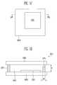
- FIG. 5Cis a schematic top plan view of an organic light emitting display in accordance with one embodiment
- FIG. 5Dis a cross-sectional view of the organic light emitting display of FIG. 5C , taken along the line d-d;
- FIG. 5Eis a schematic perspective view illustrating mass production of organic light emitting devices in accordance with one embodiment.
- OLEDorganic light emitting display
- OLEDis a display device comprising an array of organic light emitting diodes.
- Organic light emitting diodesare solid state devices which include an organic material and are adapted to generate and emit light when appropriate electrical potentials are applied.
- FIG. 5Aschematically illustrates an exploded view of a simplified structure of a passive matrix type OLED 1000 .
- FIG. 5Bschematically illustrates a simplified structure of an active matrix type OLED 1001 .
- the OLED 1000 , 1001includes OLED pixels built over a substrate 1002 , and the OLED pixels include an anode 1004 , a cathode 1006 and an organic layer 1010 .
- an appropriate electrical currentis applied to the anode 1004 , electric current flows through the pixels and visible light is emitted from the organic layer.
- the passive matrix OLED (PMOLED) designincludes elongate strips of anode 1004 arranged generally perpendicular to elongate strips of cathode 1006 with organic layers interposed therebetween.
- the intersections of the strips of cathode 1006 and anode 1004define individual OLED pixels where light is generated and emitted upon appropriate excitation of the corresponding strips of anode 1004 and cathode 1006 .
- PMOLEDsprovide the advantage of relatively simple fabrication.
- the active matrix OLEDincludes local driving circuits 1012 arranged between the substrate 1002 and an array of OLED pixels.
- An individual pixel of AMOLEDsis defined between the common cathode 1006 and an anode 1004 , which is electrically isolated from other anodes.
- Each driving circuit 1012is coupled with an anode 1004 of the OLED pixels and further coupled with a data line 1016 and a scan line 1018 .
- the scan lines 1018supply scan signals that select rows of the driving circuits
- the data lines 1016supply data signals for particular driving circuits.
- the data signals and scan signalsstimulate the local driving circuits 1012 , which excite the anodes 1004 so as to emit light from their corresponding pixels.
- the local driving circuits 1012 , the data lines 1016 and scan lines 1018are buried in a planarization layer 1014 , which is interposed between the pixel array and the substrate 1002 .
- the planarization layer 1014provides a planar top surface on which the organic light emitting pixel array is formed.
- the planarization layer 1014may be formed of organic or inorganic materials, and formed of two or more layers although shown as a single layer.
- the local driving circuits 1012are typically formed with thin film transistors (TFT) and arranged in a grid or array under the OLED pixel array.
- the local driving circuits 1012may be at least partly made of organic materials, including organic TFT.
- AMOLEDshave the advantage of fast response time improving their desirability for use in displaying data signals. Also, AMOLEDs have the advantages of consuming less power than passive matrix OLEDs.
- the substrate 1002provides structural support for the OLED pixels and circuits.
- the substrate 1002can comprise rigid or flexible materials as well as opaque or transparent materials, such as plastic, glass, and/or foil.
- each OLED pixel or diodeis formed with the anode 1004 , cathode 1006 and organic layer 1010 interposed therebetween.
- the cathode 1006injects electrons and the anode 1004 injects holes.
- the anode 1004 and cathode 1006are inverted; i.e., the cathode is formed on the substrate 1002 and the anode is opposingly arranged.
- Interposed between the cathode 1006 and anode 1004are one or more organic layers. More specifically, at least one emissive or light emitting layer is interposed between the cathode 1006 and anode 1004 .
- the light emitting layermay comprise one or more light emitting organic compounds. Typically, the light emitting layer is configured to emit visible light in a single color such as blue, green, red or white.
- one organic layer 1010is formed between the cathode 1006 and anode 1004 and acts as a light emitting layer.
- Additional layers, which can be formed between the anode 1004 and cathode 1006can include a hole transporting layer, a hole injection layer, an electron transporting layer and an electron injection layer.
- Hole transporting and/or injection layerscan be interposed between the light emitting layer 1010 and the anode 1004 . Electron transporting and/or injecting layers can be interposed between the cathode 1006 and the light emitting layer 1010 .
- the electron injection layerfacilitates injection of electrons from the cathode 1006 toward the light emitting layer 1010 by reducing the work function for injecting electrons from the cathode 1006 .
- the hole injection layerfacilitates injection of holes from the anode 1004 toward the light emitting layer 1010 .
- the hole and electron transporting layersfacilitate movement of the carriers injected from the respective electrodes toward the light emitting layer.
- a single layermay serve both electron injection and transportation functions or both hole injection and transportation functions. In some embodiments, one or more of these layers are lacking. In some embodiments, one or more organic layers are doped with one or more materials that help injection and/or transportation of the carriers. In embodiments where only one organic layer is formed between the cathode and anode, the organic layer may include not only an organic light emitting compound but also certain functional materials that help injection or transportation of carriers within that layer.
- organic materialsthat have been developed for use in these layers including the light emitting layer. Also, numerous other organic materials for use in these layers are being developed. In some embodiments, these organic materials may be macromolecules including oligomers and polymers. In some embodiments, the organic materials for these layers may be relatively small molecules. The skilled artisan will be able to select appropriate materials for each of these layers in view of the desired functions of the individual layers and the materials for the neighboring layers in particular designs.
- an electrical circuitprovides appropriate potential between the cathode 1006 and anode 1004 . This results in an electrical current flowing from the anode 1004 to the cathode 1006 via the interposed organic layer(s).
- the cathode 1006provides electrons to the adjacent organic layer 1010 .
- the anode 1004injects holes to the organic layer 1010 .
- the holes and electronsrecombine in the organic layer 1010 and generate energy particles called “excitons.”
- the excitonstransfer their energy to the organic light emitting material in the organic layer 1010 , and the energy is used to emit visible light from the organic light emitting material.
- the spectral characteristics of light generated and emitted by the OLED 1000 , 1001depend on the nature and composition of organic molecules in the organic layer(s).
- the composition of the one or more organic layerscan be selected to suit the needs of a particular application by one of ordinary skill in the art.
- OLED devicescan also be categorized based on the direction of the light emission.
- top emission typeOLED devices emit light and display images through the cathode or top electrode 1006 .
- the cathode 1006is made of a material transparent or at least partially transparent with respect to visible light.
- the anodemay be made of a material substantially reflective of the visible light.
- a second type of OLED devicesemits light through the anode or bottom electrode 1004 and is called “bottom emission” type.
- the anode 1004is made of a material which is at least partially transparent with respect to visible light.
- the cathode 1006is made of a material substantially reflective of the visible light.
- a third type of OLED devicesemits light in two directions, e.g. through both anode 1004 and cathode 1006 .
- the substratemay be formed of a material which is transparent, opaque or reflective of visible light.
- an OLED pixel array 1021comprising a plurality of organic light emitting pixels is arranged over a substrate 1002 as shown in FIG. 5C .
- the pixels in the array 1021are controlled to be turned on and off by a driving circuit (not shown), and the plurality of the pixels as a whole displays information or image on the array 1021 .
- the OLED pixel array 1021is arranged with respect to other components, such as drive and control electronics to define a display region and a non-display region.
- the display regionrefers to the area of the substrate 1002 where OLED pixel array 1021 is formed.
- the non-display regionrefers to the remaining areas of the substrate 1002 .
- the non-display regioncan contain logic and/or power supply circuitry. It will be understood that there will be at least portions of control/drive circuit elements arranged within the display region. For example, in PMOLEDs, conductive components will extend into the display region to provide appropriate potential to the anode and cathodes. In AMOLEDs, local driving circuits and data/scan lines coupled with the driving circuits will extend into the display region to drive and control the individual pixels of the AMOLEDs.
- FIG. 5Dschematically illustrates a cross-section of an encapsulated OLED device 1011 having a layout of FIG. 5C and taken along the line d-d of FIG. 5C .
- a generally planar top plate or substrate 1061engages with a seal 1071 which further engages with a bottom plate or substrate 1002 to enclose or encapsulate the OLED pixel array 1021 .
- one or more layersare formed on the top plate 1061 or bottom plate 1002 , and the seal 1071 is coupled with the bottom or top substrate 1002 , 1061 via such a layer.
- the seal 1071extends along the periphery of the OLED pixel array 1021 or the bottom or top plate 1002 , 1061 .
- the seal 1071is made of a frit material as will be further discussed below.
- the top and bottom plates 1061 , 1002comprise materials such as plastics, glass and/or metal foils which can provide a barrier to passage of oxygen and/or water to thereby protect the OLED pixel array 1021 from exposure to these substances.
- at least one of the top plate 1061 and the bottom plate 1002are formed of a substantially transparent material.
- seal 1071 and the top and bottom plates 1061 , 1002provide a substantially non-permeable seal to oxygen and water vapor and provide a substantially hermetically enclosed space 1081 .
- the seal 1071 of a frit material in combination with the top and bottom plates 1061 , 1002provide a barrier to oxygen of less than approximately 10 ⁇ 3 cc/m 2 -day and to water of less than 10 ⁇ 6 g/m 2 -day.
- a material that can take up oxygen and/or moistureis formed within the enclosed space 1081 .
- the seal 1071has a width W, which is its thickness in a direction parallel to a surface of the top or bottom substrate 1061 , 1002 as shown in FIG. 5D .
- the widthvaries among embodiments and ranges from about 300 ⁇ m to about 3000 ⁇ m, optionally from about 500 ⁇ m to about 1500 ⁇ m. Also, the width may vary at different positions of the seal 1071 . In some embodiments, the width of the seal 1071 may be the largest where the seal 1071 contacts one of the bottom and top substrate 1002 , 1061 or a layer formed thereon. The width may be the smallest where the seal 1071 contacts the other.
- the width variation in a single cross-section of the seal 1071relates to the cross-sectional shape of the seal 1071 and other design parameters.
- the seal 1071has a height H, which is its thickness in a direction perpendicular to a surface of the top or bottom substrate 1061 , 1002 as shown in FIG. 5D .
- the heightvaries among embodiments and ranges from about 2 ⁇ m to about 30 ⁇ m, optionally from about 10 ⁇ m to about 15 ⁇ m. Generally, the height does not significantly vary at different positions of the seal 1071 . However, in certain embodiments, the height of the seal 1071 may vary at different positions thereof.
- the seal 1071has a generally rectangular cross-section. In other embodiments, however, the seal 1071 can have other various cross-sectional shapes such as a generally square cross-section, a generally trapezoidal cross-section, a cross-section with one or more rounded edges, or other configuration as indicated by the needs of a given application. To improve hermeticity, it is generally desired to increase the interfacial area where the seal 1071 directly contacts the bottom or top substrate 1002 , 1061 or a layer formed thereon. In some embodiments, the shape of the seal can be designed such that the interfacial area can be increased.
- the seal 1071can be arranged immediately adjacent the OLED array 1021 , and in other embodiments, the seal 1071 is spaced some distance from the OLED array 1021 .
- the seal 1071comprises generally linear segments that are connected together to surround the OLED array 1021 . Such linear segments of the seal 1071 can extend, in certain embodiments, generally parallel to respective boundaries of the OLED array 1021 .
- one or more of the linear segments of the seal 1071are arranged in a non-parallel relationship with respective boundaries of the OLED array 1021 .
- at least part of the seal 1071extends between the top plate 1061 and bottom plate 1002 in a curvilinear manner.
- the seal 1071is formed using a frit material or simply “frit” or “glass frit,” which includes fine glass particles.
- the frit particlesincludes one or more of magnesium oxide (MgO), calcium oxide (CaO), barium oxide (BaO), lithium oxide (Li 2 O), sodium oxide (Na 2 O), potassium oxide (K 2 O), boron oxide (B 2 O 3 ), vanadium oxide (V 2 O 5 ), zinc oxide (ZnO), tellurium oxide (TeO 2 ), aluminum oxide (Al 2 O 3 ), silicon dioxide (SiO 2 ), lead oxide (PbO), tin oxide (SnO), phosphorous oxide (P 2 O 5 ), ruthenium oxide (Ru 2 O), rubidium oxide (Rb 2 O), rhodium oxide (Rh 2 O), ferrite oxide (Fe 2 O 3 ), copper oxide (CuO), titanium oxide (TiO 2 ), tungsten oxide (WO 3 ), bismuth oxide (Bi
- MgOmagnesium
- these particlesrange in size from about 2 ⁇ m to about 30 ⁇ m, optionally about 5 ⁇ m to about 10 ⁇ m, although not limited only thereto.
- the particlescan be as large as about the distance between the top and bottom substrates 1061 , 1002 or any layers formed on these substrates where the frit seal 1071 contacts.
- the frit material used to form the seal 1071can also include one or more filler or additive materials.
- the filler or additive materialscan be provided to adjust an overall thermal expansion characteristic of the seal 1071 and/or to adjust the absorption characteristics of the seal 1071 for selected frequencies of incident radiant energy.
- the filler or additive material(s)can also include inversion and/or additive fillers to adjust a coefficient of thermal expansion of the frit.
- the filler or additive materialscan include transition metals, such as chromium (Cr), iron (Fe), manganese (Mn), cobalt (Co), copper (Cu), and/or vanadium. Additional materials for the filler or additives include ZnSiO 4 , PbTiO 3 , ZrO 2 , eucryptite.
- a frit material as a dry compositioncontains glass particles from about 20 to 90 about wt %, and the remaining includes fillers and/or additives.
- the frit pastecontains about 10-30 wt % organic materials and about 70-90% inorganic materials.
- the frit pastecontains about 20 wt % organic materials and about 80 wt % inorganic materials.
- the organic materialsmay include about 0-30 wt % binder(s) and about 70-100 wt % solvent(s).
- about 10 wt %is binder(s) and about 90 wt % is solvent(s) among the organic materials.
- the inorganic materialsmay include about 0-10 wt % additives, about 20-40 wt % fillers and about 50-80 wt % glass powder. In some embodiments, about 0-5 wt % is additive(s), about 25-30 wt % is filler(s) and about 65-75 wt % is the glass powder among the inorganic materials.
- a liquid materialis added to the dry frit material to form a frit paste.
- Any organic or inorganic solvent with or without additivescan be used as the liquid material.
- the solventincludes one or more organic compounds.
- applicable organic compoundsare ethyl cellulose, nitro cellulose, hydroxyl propyl cellulose, butyl carbitol acetate, terpineol, butyl cellusolve, acrylate compounds.
- a shape of the seal 1071is initially formed from the frit paste and interposed between the top plate 1061 and the bottom plate 1002 .
- the seal 1071can in certain embodiments be pre-cured or pre-sintered to one of the top plate and bottom plate 1061 , 1002 .
- portions of the seal 1071are selectively heated such that the frit material forming the seal 1071 at least partially melts.
- the seal 1071is then allowed to resolidify to form a secure joint between the top plate 1061 and the bottom plate 1002 to thereby inhibit exposure of the enclosed OLED pixel array 1021 to oxygen or water.
- the selective heating of the frit sealis carried out by irradiation of light, such as a laser or directed infrared lamp.
- the frit material forming the seal 1071can be combined with one or more additives or filler such as species selected for improved absorption of the irradiated light to facilitate heating and melting of the frit material to form the seal 1071 .
- OLED devices 1011are mass produced.
- a plurality of separate OLED arrays 1021is formed on a common bottom substrate 1101 .
- each OLED array 1021is surrounded by a shaped frit to form the seal 1071 .
- common top substrate(not shown) is placed over the common bottom substrate 1101 and the structures formed thereon such that the OLED arrays 1021 and the shaped frit paste are interposed between the common bottom substrate 1101 and the common top substrate.
- the OLED arrays 1021are encapsulated and sealed, such as via the previously described enclosure process for a single OLED display device.
- the resulting productincludes a plurality of OLED devices kept together by the common bottom and top substrates.
- the resulting productis cut into a plurality of pieces, each of which constitutes an OLED device 1011 of FIG. 5D .
- the individual OLED devices 1011then further undergo additional packaging operations to further improve the sealing formed by the frit seal 1071 and the top and bottom substrates 1061 , 1002 .
- FIG. 1is a cross-sectional view showing encapsulating structure that can prevent moisture from containing organic materials.
- the organic light-emitting display deviceincludes a substrate 1 , an encapsulation substrate 2 , an sealing member 3 and moisture absorbent 4 .
- the substrate 1includes at least one organic light-emitting diode (not shown), and the encapsulation substrate 2 is attached to the substrate 1 to oppose the organic light-emitting diode formed on the substrate 1 .
- the sealing material 3is applied along the edge of the substrate 1 and the encapsulation substrate 2 , and the sealing material is cured using UV irradiation, etc.
- the moisture absorbent 4is included within the encapsulation substrate 2 for removing them for capturing moisture and certain gases such as hydrogen, oxygen. Even in the illustrated device, however, the sealing material 3 may not completely prevent moisture or air entering into the enclosed space. Also, there may be cracks in the sealing material 3 and in the interfacial area where the sealing material 3 contacts the substrate for various reasons.
- the organic light emitting display devicehas a gap between the top surface of the array and the inner surface of the top substrate.
- the size of the gapdepends on the height of the seal interconnecting two substrates.
- a frit sealamong other forms of sealing, allows the gap size significantly smaller than others.
- the gap size(the distance between the array and the second substrate) can be in the order of a few ⁇ m to several hundred ⁇ m.
- dark rings called Newton ringsmay be formed on the display surface due to optical interference created by light incident to the display surface. More specifically, when the gap size is about or less than 10 ⁇ m, the possibility of Newton rings may increase.
- the configuration for avoiding Newton ringscan be a design factor.
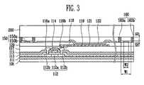
- FIG. 2is a plan view of an organic light-emitting display device according to an embodiment of the present invention and FIG. 3 is a cross-sectional view of an organic light-emitting display device taken along the A-A′ line of FIG. 2 .
- an organic light-emitting display devicecomprises a bottom substrate 100 , an encapsulation or top substrate 200 , encapsulating or sealing member 150 and supplement material or structure 160 .
- the deposition substrate 101refers to a base, on which circuits and layers are formed
- the substrate 100refers to an unfinished product including the deposition substrate 101 and circuits and layers formed thereon, including an array of organic light emitting pixels.
- the substrate 100which is a plate including organic light-emitting diodes or pixels, comprises a pixel region 100 a in which at least one organic light-emitting configured of a first electrode 119 , an organic layer 121 and a second electrode 122 is formed, and a non-pixel region 100 formed outside the pixel region 100 a .
- the pixel region 100 ameans a region in which a predetermined image is displayed by light emitted from the organic light-emitting diode
- the non-pixel region 100 bmeans all regions other than the pixel region 100 a on the substrate 100 .
- the pixel region 100 aincludes a plurality of scan lines (S 1 to Sm) arranged in a row direction and a plurality of data lines (D 1 to Dm) arranged in a column direction, and a plurality of pixels receiving a signal from a driver integrated circuit 300 , 400 for driving the organic light-emitting diode are formed in the scan lines (S 1 to Sm) and the data lines (D 1 to Dm).
- driver ICs 300 and 400 for driving the organic light-emitting diodea scan supplying line 410 and a data supplying line 310 electrically connected to the scan lines (S 1 to Sm) and the data lines (D 1 to Dm) of the pixel region, respectively; and a power line (not shown), etc. are formed.
- the data driver 300which can be mounted on the substrate 100 by being prepared in the form of a chip, is electrically connected to a second pad Pd of a pad part 500 .
- Such a data driver 300receives a signal from the second pad Pd through the data supplying line 310 and transmits the data signal to a plurality of data lines (D 1 ,D 2 , . .
- the scan driver 400is formed to be adjacent to one side of the pixel region 100 a and is electrically connected to a first pad Ps of the pad part 500 through the scan supplying line 410 .
- Such a scan driver 400receives a signal from the first pad Ps through the scan supplying line 410 and supplies the scan signal to a plurality of scan lines (S 1 ,S 2 , . . . Sn) in sequence.
- the pad part 500supplies a driving power to the data driver 300 through the data supplying line 310 and supplies the driving power to the scan driver 400 through the scan supplying line 410 .
- the drawingsillustrate the case that the data driver 300 , the scan driver 400 and the pad part 500 are not encapsulated since the encapsulating member 150 are applied along the outer of the pixel region 100 a , however, the present invention is not limited thereto and the encapsulating member 150 can be applied along the all outers of the data driver 300 , the scan driver 400 and the pad part 500 according to designs.
- the size of the encapsulation substrate 200will be also prepared in size capable of sealing all sides of the substrate 100 .
- the organic light-emitting display deviceis illustrated to be driven in an active matrix approach in the present drawings, therefore, the structure thereof will be schematically explained.
- a buffer layer 111is formed on a base substrate 101 , and the buffer layer 111 is made of insulating material such as silicon oxide SiO2 or silicon nitride Sinx, etc.
- the buffer layer 111is formed to prevent the substrate 100 from damaging due to factors such as heat from outside, etc.
- a semiconductor layer 112comprising an active layer 112 a and an ohmic contact layer 112 b is formed.
- a gate insulating layer 113is formed, and on one region of the gate insulating layer 113 a gate electrode 114 having the size corresponding to the width of the active layer 112 is formed.
- An interlayer insulating layer 115is formed on the gate insulating layer 113 including the gate electrode 114 , and source and drain electrodes 116 a , 116 b are formed on a predetermined region on the interlayer insulating layer 115 .
- the source and drain electrodes 116 a , 116 bare formed to connect to one region in which the ohmic contact layer 112 b is exposed, respectively, and a planarization layer 117 is formed on the interlayer insulating layer 115 including the source and drain electrodes 116 a , 116 b .
- a first electrode 119is formed and at this time, the first electrode 119 is connected to one region exposed to any one of source and drain electrodes 116 a , 116 b by means of a via hole 118 .
- a pixel defined film 120having an opening part (not shown) exposing at least one region of the first electrode 119 is formed.
- the active type matrix structure or the passive matrix structure of the organic light-emitting diodecan variously be modified and the respective general structures have been well known, and therefore, the detailed explanation thereof will be omitted.
- the encapsulation or top substrate 200which is attached to the substrate 100 for encapsulating the organic light-emitting diodes formed on the substrate 100 , can be made of transparent material in the case of front side light-emitting type or both sides light-emitting type of the OLED device, and be made of opaque material in the case of rear side light-emitting type of the OLED device. Although not limited thereto, in an embodiment, glass can be used in the case of the front side light-emitting type.
- the encapsulation substrate 200is configured as a plate-type in an embodiment, and the encapsulation substrate 200 seals the region including the pixel region 100 a in which the organic light-emitting diode of the substrate is formed.
- the sealing material or member 150which is formed in the space or gap between the encapsulation substrate 200 and the non-pixel region 100 b of the substrate 100 , encapsulates the pixel region 100 a so that air or moisture cannot move into, and, in an embodiment, forms a line spaced from an edge of the side. This provides a space to form second sealing member 160 to be described later.
- the encapsulating member 150comprises a first frit layer 150 a and a second frit layer 150 b integrated with the first frit layer 150 a .
- the second frit layer 150 bmelts substantially easier than the first frit layer 150 a upon irradiation of a laser or infrared beam thereto.
- the composition of materials forming the second frit layer 150 bis to melt quicker than the composition of materials forming the first frit layer 150 a .
- the time required to start the second frit layer 150 b to meltis about 10, 20, 30, 40, 50, 55, 60, 65, 70, 75, 80 or 90% of the time required to start the first frit layer 150 a to melt.
- the composition of materials forming the second frit layer 150 bis to melt at a less powerful beam than the composition of materials forming the first frit layer 150 a .
- the energy of the laser or infrared beam required to start the second frit layer 150 b to meltis about 10, 20, 30, 40, 50, 55, 60, 65, 70, 75, 80 or 90% of the energy of the beam required to start the first frit layer 150 a to melt when applied for the same period of time.
- the first frit layer 150 amay be transparent and the second frit layer 150 b may be opaque.
- the first frit layer 150 awhich is transparent, for example, made of silicon oxide SiO2, functions as a spacer for controlling the gap or space between the substrate 100 and the encapsulation substrate 200 and accordingly, keeps the gap distance between the substrate 100 and the encapsulation substrate 200 constant, thereby, preventing the generation of a Newton's ring phenomenon.
- the Newton's ring phenomenonis a phenomenon that the pattern of a concentric circle from a contact point of the substrate may be formed due to an optical interference phenomenon and such a pattern of a concentric circle may be displayed on a display surface.
- the first frit layer 150 aprevents a generation of the Newton's ring phenomenon by providing the gap distance between the substrate 100 and the encapsulation substrate 200 greater than a certain gap distance which may generate Newton's ring.
- the second frit layer 150 bcomprising absorbent capable of absorbing energy of laser or infrared rays, melts between the encapsulation substrate 200 and the substrate 100 by absorbing the irradiated energy, bonding the encapsulation substrate 200 to the substrate 100 . That is, when laser or infrared rays are irradiated to the encapsulating member 150 , the transparent first frit layer 150 a allows the laser or the infrared rays to pass through and the second frit layer 150 b melts and cured by using the irradiation of the laser or the infrared rays, thereby encapsulating the space between the substrate 100 and the encapsulation substrate 200 .
- the reason why the encapsulating member 150 is configured of a double layer as aboveis to improve efficiency of the irradiation of laser of infrared rays.
- the height H 1 of the first frit layer 150 ais from about 5 ⁇ m to about 100 ⁇ m
- height H 2 of the second frit layer 150 bis from about 3 ⁇ m to about 5 ⁇ m, although not limited thereto.
- the width W 2 of the second frit layeris formed to be smaller than the width W 1 of the first frit layer.
- the width W 1 of the first frit layeris from about 0.5 mm to about 1.5 mm.
- the region on the substrate on which the encapsulating member 150 is formedis not overlapped with metal wiring. Since the encapsulating member 150 is irradiated with laser or infrared rays as described above, the metal wiring may be damaged when the encapsulating member 150 is overlapped with the metal wiring.
- the supplementary material or structure 160which is formed on the outer side, the inner side, or the both sides of the encapsulating member 150 , prevents the organic light-emitting display device from easily breaking, in particular, when all the substrate 100 , the encapsulation substrate 200 and the encapsulating member 150 are glass.
- the supplement materialserves as an additional sealing member, in particular, when the encapsulating member 150 is damaged by being melted and its adhesion is weaken.
- the supplement material 160can be apart from the encapsulating member 150 at a predetermined interval or contact to the encapsulating member 150 .
- resins which are naturally cured, thermally cured or UV cured by being applied in liquid statecan be used.
- acrylate cyanideas material to be naturally cured
- acrylateas material to be thermally cured at a temperature less than 80° C.
- epoxyacrylate and urethane acrylate as material to be UV cured
- the width of the supplement materialis associated with the width of the encapsulating member, and in an embodiment, it is from about 0.3 mm to about 0.7 mm as described above.
- FIG. 4 a to FIG. 4 eare views for illustrating steps of the process of making the organic light-emitting display device.
- the first frit layer 150 a of transparent materialis formed on one region of the encapsulation substrate 200 .
- the first frit layer 150 acan be applied with a dispenser or a screen printing method.
- the first frit layer 150 ais baked at a predetermined temperature. In one embodiment, the temperature for baking the first frit layer 150 a is from about 450° C. to about 600° C. After baking process of the first frit layer 150 a , the interfaces of the encapsulation substrate 200 and the first frit layer 150 a are bonded.
- FIG. 4 bis bonded.
- the second frit layer 150 b of opaque materialis applied to one region on the first frit layer 150 a .
- the width of the second frit layer 150 bcan be identical or narrower than that of the first frit layer 150 a .
- the second frit layer 150 bcan be applied in the same manner as in the first frit layer.
- the second frit layer 150 bis baked at a predetermined temperature. In one embodiment, the second frit layer 150 b may be baked in the same range of temperature with the baking of the first frit layer 150 a . After baking process, the first frit layer 150 a , the encapsulation substrate 200 and the second frit layer 150 b are integrated. ( FIG. 4 d )
- the supplement materialis applied to the substrate 200 at the inner side or the outer side, or to the both sides.
- the supplement member 160 a and 160 bare formed on both the inner side and the outer side.
- the supplement material 160is resin material to be cured in the step described below.
- the substrate 100is bonded to the encapsulation substrate 200 .
- the substrate 100comprises the pixel region in which the organic light-emitting diode is formed and the non-pixel region including regions other than the pixel region, and the encapsulation substrate 200 is bonded to the substrate to seal the pixel region of the substrate.
- the supplement material 160is heated or irradiated by ultraviolet rays to be cured, primarily bonding the encapsulation substrate 200 to the substrate 100 .
- the encapsulating member 150is irradiated with laser or infrared rays and the second frit layer of the encapsulating member 150 is melted by absorbing the energy of laser or infrared rays. Thereafter, the second frit layer 150 b melted is cured, thereby bonding the encapsulation substrate 200 to the substrate 100 .
- the wavelength thereofis from about 800 to about 1200 nm (preferably, about 810 nm)
- the output thereofis from about 25 to about 45 watt and the parts other than the frit is to be masked.
- the encapsulating member 150 formed on the encapsulation substrate 200is explained, although is not limited thereto.
- the encapsulating member 150can be formed on the substrate 100 .
- the second frit layer 150 b formed on the first frit layer 150 a so that laser or infrared rays can be irradiated to the second frit layer 150 b and laser or infrared rays pass through the first frit layer 150 ais explained, the positions of the first frit layer 150 a and the second frit layer 150 may be changed.
- each of the first frit layer and the second frit layermay be formed to have a plurality of layers.
- the laser or the infrared raysmay be irradiated to the side of the substrate or its opposite side.
Landscapes
- Physics & Mathematics (AREA)
- Optics & Photonics (AREA)
- Engineering & Computer Science (AREA)
- Manufacturing & Machinery (AREA)
- Electroluminescent Light Sources (AREA)
Abstract
Description
| Application | |||
| Title | Atty. Docket No. | Filing Date | No. |
| ORGANIC LIGHT-EMITTING DISPLAY | SDISHN.043AUS | ||
| DEVICE AND METHOD OF | |||
| FABRICATING THE SAME | |||
| ORGANIC LIGHT-EMITTING DISPLAY | SDISHN.045AUS | ||
| DEVICE AND METHOD OF | |||
| MANUFACTURING THE SAME | |||
| ORGANIC LIGHT EMITTING DISPLAY | SDISHN.048AUS | ||
| DEVICE | |||
| ORGANIC LIGHT-EMITTING DISPLAY | SDISHN.051AUS | ||
| DEVICE WITH FRIT SEAL AND | |||
| REINFORCING STRUCTURE | |||
| ORGANIC LIGHT EMITTING DISPLAY | SDISHN.052AUS | ||
| DEVICE METHOD OF FABRICATING | |||
| THE SAME | |||
| ORGANIC LIGHT EMITTING DISPLAY | SDISHN.053AUS | ||
| AND METHOD OF FABRICATING THE | |||
| SAME | |||
| ORGANIC LIGHT-EMITTING DISPLAY | SDISHN.054AUS | ||
| DEVICE WITH FRIT SEAL AND | |||
| REINFORCING STRUCTURE BONDED | |||
| TO FRAME | |||
| METHOD FOR PACKAGING ORGANIC | SDISHN.055AUS | ||
| LIGHT EMITTING DISPLAY WITH | |||
| FRIT SEAL AND REINFORCING | |||
| STURUTURE | |||
| METHOD FOR PACKAGING ORGANIC | SDISHN.056AUS | ||
| LIGHT EMITTING DISPLAY WITH | |||
| FRIT SEAL AND REINFORCING | |||
| STURUTURE | |||
| ORGANIC LIGHT EMITTING DISPLAY | SDISHN.061AUS | ||
| AND FABRICATING METHOD OF THE | |||
| SAME | |||
| ORGANIC LIGHT-EMITTING DISPLAY | SDISHN.062AUS | ||
| AND METHOD OF MAKING THE | |||
| SAME | |||
| ORGANIC LIGHT EMITTING DISPLAY | SDISHN.063AUS | ||
| AND FABRICATING METHOD OF THE | |||
| SAME | |||
| ORGANIC LIGHT EMITTING DISPLAY | SDISHN.064AUS | ||
| DEVICE AND MANUFACTURING | |||
| METHOD THEREOF | |||
| ORGANIC LIGHT-EMITTING DISPLAY | SDISHN.066AUS | ||
| DEVICE AND MANUFACTURING | |||
| METHOD OF THE SAME | |||
| ORGANIC LIGHT EMITTING DISPLAY | SDISHN.067AUS | ||
| AND FABRICATING METHOD OF THE | |||
| SAME | |||
| ORGANIC LIGHT EMITTING DISPLAY | SDISW.017AUS | ||
| AND METHOD OF FABRICATING THE | |||
| SAME | |||
| ORGANIC LIGHT EMITTING DISPLAY | SDISW.018AUS | ||
| DEVICE METHOD OF FABRICATING | |||
| THE SAME | |||
| ORGANIC LIGHT EMITTING DISPLAY | SDISW.020AUS | ||
| AND METHOD OF FABRICATING THE | |||
| SAME | |||
Claims (20)
Applications Claiming Priority (2)
| Application Number | Priority Date | Filing Date | Title |
|---|---|---|---|
| KR10-2006-0028571 | 2006-03-29 | ||
| KR1020060028571AKR100732817B1 (en) | 2006-03-29 | 2006-03-29 | Organic light emitting display device and manufacturing method |
Publications (2)
| Publication Number | Publication Date |
|---|---|
| US20070232182A1 US20070232182A1 (en) | 2007-10-04 |
| US7837530B2true US7837530B2 (en) | 2010-11-23 |
Family
ID=38373559
Family Applications (1)
| Application Number | Title | Priority Date | Filing Date |
|---|---|---|---|
| US11/540,008Active2029-09-23US7837530B2 (en) | 2006-03-29 | 2006-09-29 | Method of sealing an organic light emitting display by means of a glass frit seal assembly |
Country Status (2)
| Country | Link |
|---|---|
| US (1) | US7837530B2 (en) |
| KR (1) | KR100732817B1 (en) |
Cited By (35)
| Publication number | Priority date | Publication date | Assignee | Title |
|---|---|---|---|---|
| US20070170850A1 (en)* | 2006-01-23 | 2007-07-26 | Choi Dong-Soo | Organic light emitting display and method of fabricating the same |
| US20070170861A1 (en)* | 2006-01-20 | 2007-07-26 | Jong Woo Lee | Organic light-emitting display device and manufacturing method of the same |
| US20070170855A1 (en)* | 2006-01-25 | 2007-07-26 | Choi Dong-Soo | Organic light emitting display device and method of fabricating the same |
| US20100112887A1 (en)* | 2008-10-31 | 2010-05-06 | Kwang-Min Kim | Method of making organic light emitting display device |
| US8063561B2 (en) | 2006-01-26 | 2011-11-22 | Samsung Mobile Display Co., Ltd. | Organic light emitting display device |
| US8164257B2 (en) | 2006-01-25 | 2012-04-24 | Samsung Mobile Display Co., Ltd. | Organic light emitting display and method of fabricating the same |
| US8415880B2 (en) | 2006-01-20 | 2013-04-09 | Samsung Display Co., Ltd. | Organic light-emitting display device with frit seal and reinforcing structure |
| US8623469B2 (en) | 2011-10-21 | 2014-01-07 | Semiconductor Energy Laboratory Co., Ltd. | Method of heating dispersion composition and method of forming glass pattern |
| US20140132149A1 (en)* | 2012-11-13 | 2014-05-15 | Samsung Display Co., Ltd. | Organic light emitting display apparatus and method of manufacturing the same |
| US20140225077A1 (en)* | 2013-02-13 | 2014-08-14 | Jung-I Yun | Organic light emitting diode display |
| US8816336B2 (en) | 2011-06-16 | 2014-08-26 | Semiconductor Energy Laboratory Co., Ltd. | Sealed body, method for manufacturing sealed body, light-emitting device, and method for manufacturing light-emitting device |
| US8950216B2 (en) | 2011-05-13 | 2015-02-10 | Semiconductor Energy Laboratory Co., Ltd. | Method for manufacturing glass sealed body and method for manufacturing light-emitting device |
| US9048350B2 (en) | 2011-11-28 | 2015-06-02 | Semiconductor Energy Laboratory Co., Ltd. | Sealed body, light-emitting module and method of manufacturing sealed body |
| CN104685656A (en)* | 2012-09-28 | 2015-06-03 | 欧司朗Oled股份有限公司 | Optoelectronic device and method for manufacturing an optoelectronic device |
| US20150194627A1 (en)* | 2013-07-17 | 2015-07-09 | Shenzhen China Star Optoelectronics Technology Co., Ltd. | Glass packaging structure and glass packaging method of utilizing the same |
| US20150250032A1 (en)* | 2013-04-29 | 2015-09-03 | Samsung Display Co., Ltd. | Organic light emitting display apparatus and method of manufacturing the same |
| US20150311472A1 (en)* | 2014-04-28 | 2015-10-29 | Samsung Display Co., Ltd. | Display apparatus and method of manufacturing the same |
| US20150349288A1 (en)* | 2014-05-29 | 2015-12-03 | Boe Technology Group Co., Ltd. | Light emitting display panel and manufacturing method thereof |
| US9214643B2 (en) | 2011-11-29 | 2015-12-15 | Semiconductor Energy Laboratory Co., Ltd. | Sealed structure, light-emitting device, electronic device, and lighting device |
| US9216557B2 (en) | 2011-11-29 | 2015-12-22 | Semiconductor Energy Laboratory Co., Ltd. | Sealed structure, light-emitting device, electronic device, and lighting device |
| US9258853B2 (en) | 2011-08-26 | 2016-02-09 | Semiconductor Energy Laboratory Co., Ltd. | Light-emitting device, electronic device, lighting device, and method for manufacturing the light-emitting device |
| US9299943B2 (en) | 2011-11-28 | 2016-03-29 | Semiconductor Energy Laboratory Co., Ltd. | Glass pattern and method for forming the same, sealed body and method for manufacturing the same, and light-emitting device |
| US9362522B2 (en) | 2012-10-26 | 2016-06-07 | Semiconductor Energy Laboratory Co., Ltd. | Method for bonding substrates, method for manufacturing sealing structure, and method for manufacturing light-emitting device |
| US9440880B2 (en) | 2011-06-17 | 2016-09-13 | Semiconductor Energy Laboratory Co., Ltd. | Method of manufacturing light-emitting device |
| US9472776B2 (en) | 2011-10-14 | 2016-10-18 | Semiconductor Energy Laboratory Co., Ltd. | Method for manufacturing sealed structure including welded glass frits |
| US9570703B2 (en) | 2014-03-17 | 2017-02-14 | Samsung Display Co., Ltd. | Organic light emitting display with reinforced sealing structure |
| US20170098797A1 (en)* | 2015-10-06 | 2017-04-06 | Samsung Display Co., Ltd. | Display apparatus |
| US9633871B2 (en) | 2011-08-24 | 2017-04-25 | Semiconductor Energy Laboratory Co., Ltd. | Light-emitting device |
| US9666755B2 (en) | 2011-11-29 | 2017-05-30 | Semiconductor Energy Laboratory Co., Ltd. | Method of manufacturing sealed body and method of manufacturing light-emitting device |
| US20170309823A1 (en)* | 2015-05-08 | 2017-10-26 | Boe Technology Group Co., Ltd. | Display panel and fabricating method thereof, and display device |
| US9853242B2 (en) | 2012-07-30 | 2017-12-26 | Semiconductor Energy Laboratory Co., Ltd. | Sealing structure and organic electroluminescence device |
| US10068926B2 (en) | 2011-05-05 | 2018-09-04 | Semiconductor Energy Laboratory Co., Ltd. | Semiconductor device and method for manufacturing the same |
| EP3252820A4 (en)* | 2015-01-28 | 2018-10-03 | Boe Technology Group Co. Ltd. | Oled panel and manufacturing method thereof and display device |
| US20190206960A1 (en)* | 2017-12-29 | 2019-07-04 | Lg Display Co., Ltd. | Electroluminescent display device |
| US20220059797A1 (en)* | 2018-11-05 | 2022-02-24 | Samsung Display Co., Ltd. | Display device and method of fabricating the same |
Families Citing this family (28)
| Publication number | Priority date | Publication date | Assignee | Title |
|---|---|---|---|---|
| JP4456092B2 (en)* | 2006-01-24 | 2010-04-28 | 三星モバイルディスプレイ株式會社 | Organic electroluminescent display device and manufacturing method thereof |
| KR100688795B1 (en)* | 2006-01-25 | 2007-03-02 | 삼성에스디아이 주식회사 | Organic light emitting display device and manufacturing method |
| KR100671641B1 (en) | 2006-01-25 | 2007-01-19 | 삼성에스디아이 주식회사 | Organic electroluminescent display and manufacturing method thereof |
| JP4633674B2 (en) | 2006-01-26 | 2011-02-16 | 三星モバイルディスプレイ株式會社 | Organic electroluminescent display device and manufacturing method thereof |
| KR100688790B1 (en) | 2006-01-27 | 2007-03-02 | 삼성에스디아이 주식회사 | Organic electroluminescent display and manufacturing method thereof |
| KR100671639B1 (en) | 2006-01-27 | 2007-01-19 | 삼성에스디아이 주식회사 | Organic electroluminescent display and manufacturing method thereof |
| KR100703458B1 (en)* | 2006-04-20 | 2007-04-03 | 삼성에스디아이 주식회사 | Organic light emitting display device and manufacturing method thereof |
| US8063562B2 (en)* | 2007-11-19 | 2011-11-22 | Seiko Epson Corporation | Light-emitting device and electronic apparatus |
| US7815480B2 (en)* | 2007-11-30 | 2010-10-19 | Corning Incorporated | Methods and apparatus for packaging electronic components |
| US8067883B2 (en)* | 2008-02-29 | 2011-11-29 | Corning Incorporated | Frit sealing of large device |
| JP5535652B2 (en) | 2008-06-11 | 2014-07-02 | 浜松ホトニクス株式会社 | Glass welding method |
| WO2010055888A1 (en)* | 2008-11-14 | 2010-05-20 | 旭硝子株式会社 | Method for producing glass member provided with sealing material layer, and method for manufacturing electronic device |
| DE102008063636A1 (en)* | 2008-12-18 | 2010-06-24 | Osram Opto Semiconductors Gmbh | Method for producing an organic optoelectronic component and organic optoelectronic component |
| KR101073564B1 (en)* | 2010-02-02 | 2011-10-17 | 삼성모바일디스플레이주식회사 | Organic light emitting diode display and method for manufacturing organic light emitting diode display |
| TWI503044B (en)* | 2010-04-13 | 2015-10-01 | Au Optronics Corp | Electroluminescent device package and packaging method thereof |
| KR101693347B1 (en) | 2010-12-03 | 2017-01-06 | 삼성디스플레이 주식회사 | Display apparatus and method of manufacturing display apparatus |
| TWI451610B (en)* | 2011-05-17 | 2014-09-01 | Au Optronics Corp | Mother board structure of light-emitting device, light-emitting device and method of manufacturing same |
| KR101420332B1 (en)* | 2012-11-14 | 2014-07-16 | 삼성디스플레이 주식회사 | Organic light emitting display apparatus |
| JP6182985B2 (en)* | 2013-06-05 | 2017-08-23 | セイコーエプソン株式会社 | Electro-optical device, method of manufacturing electro-optical device, and electronic apparatus |
| KR20150043080A (en) | 2013-10-14 | 2015-04-22 | 삼성디스플레이 주식회사 | Organic light emitting display |
| KR102283856B1 (en) | 2013-11-22 | 2021-08-03 | 삼성디스플레이 주식회사 | Organic Light Emitting Display and Fabrication Method for the same |
| CN104466034A (en)* | 2014-12-15 | 2015-03-25 | 京东方科技集团股份有限公司 | Laser sintering device and sintering method |
| KR102465503B1 (en)* | 2015-04-03 | 2022-11-10 | 삼성디스플레이 주식회사 | Light emitting display device and method of manufacturing the same |
| CN105161515B (en)* | 2015-08-11 | 2018-03-23 | 京东方科技集团股份有限公司 | Organic LED display panel and its method for packing, display device |
| CN105097885B (en)* | 2015-09-01 | 2018-07-27 | 京东方科技集团股份有限公司 | Oled panel and its packaging method, display device |
| CN107275515B (en)* | 2017-06-20 | 2019-12-03 | 深圳市华星光电技术有限公司 | OLED device packaging method, structure, OLED device and display screen |
| KR102127763B1 (en)* | 2020-01-21 | 2020-06-30 | 삼성디스플레이 주식회사 | Organic light emitting diode display |
| KR102557687B1 (en)* | 2021-03-19 | 2023-07-24 | 주식회사 베이스 | Glass composition for sealing organic light emitting display |
Citations (132)
| Publication number | Priority date | Publication date | Assignee | Title |
|---|---|---|---|---|
| US3966449A (en) | 1975-02-10 | 1976-06-29 | International Business Machines Corporation | Sealing glass composition and process |
| US4105292A (en) | 1975-09-02 | 1978-08-08 | Minnesota Mining And Manufacturing Company | Optical element to assure a minimum spacing |
| US4702566A (en) | 1984-04-12 | 1987-10-27 | Asahi Glass Company Ltd. | Electrochromic display device |
| US4826297A (en) | 1985-12-25 | 1989-05-02 | Hitachi, Ltd. | Liquid crystal display device having an extention metal film wiring which is covered by polyimide layer having low viscosity under 1.0 poise before curing |
| US4984059A (en) | 1982-10-08 | 1991-01-08 | Fujitsu Limited | Semiconductor device and a method for fabricating the same |
| JPH0337933A (en)* | 1989-07-04 | 1991-02-19 | Mitsubishi Electric Corp | Manufacture of discharge-in-gas type display panel |
| JPH04301879A (en)* | 1991-03-29 | 1992-10-26 | Okaya Electric Ind Co Ltd | Display panel and its production |
| US5808719A (en) | 1994-09-02 | 1998-09-15 | Sharp Kabushiki Kaisha | Liquid crystal display apparatus wherein plurality display panels makes display surfaces flush by perming junction panel and producing method thereof |
| US5811927A (en) | 1996-06-21 | 1998-09-22 | Motorola, Inc. | Method for affixing spacers within a flat panel display |
| US5965907A (en) | 1997-09-29 | 1999-10-12 | Motorola, Inc. | Full color organic light emitting backlight device for liquid crystal display applications |
| US6005653A (en) | 1997-10-09 | 1999-12-21 | Nec Corporation | Method and apparatus for sealing liquid crystal display element cell |
| US6087717A (en) | 1997-03-24 | 2000-07-11 | Texas Instruments Incorporated | Semiconductor device and manufacturing method |
| US6195142B1 (en) | 1995-12-28 | 2001-02-27 | Matsushita Electrical Industrial Company, Ltd. | Organic electroluminescence element, its manufacturing method, and display device using organic electroluminescence element |
| US6210815B1 (en) | 1997-12-17 | 2001-04-03 | Nec Corporation | Organic thin film EL device and method for making the same |
| US6211938B1 (en) | 1997-09-18 | 2001-04-03 | Nec Corporation | Apparatus for manufacturing a plurality of liquid crystal panels using press and pressurized regions |
| CN1290121A (en) | 1999-09-27 | 2001-04-04 | 索尼株式会社 | Printed circuit board and display device |
| US6288487B1 (en) | 1999-03-17 | 2001-09-11 | Tdk Corporation | Organic electroluminescent device with a high-resistance inorganic electron injecting and transporting layer |
| JP2002020169A (en) | 2000-07-03 | 2002-01-23 | Murata Mfg Co Ltd | High-frequecy dielectric porcelain composition, dielectric resonator, dielectric filter, dielectric duplexer and communications equipment |
| JP2002117777A (en) | 2000-10-11 | 2002-04-19 | Matsushita Electric Ind Co Ltd | Gas discharge panel and its manufacturing method |
| JP2002170664A (en) | 2000-12-05 | 2002-06-14 | Toray Ind Inc | Organic electroluminescent device |
| US6452323B1 (en) | 1999-09-20 | 2002-09-17 | Omnion Technologies, Inc. | Luminous gas discharge display having dielectric sealing layer |
| US6489719B1 (en) | 1999-06-03 | 2002-12-03 | Koninklijke Philips Electronics N.V. | Organic electroluminescent device |
| US6495262B2 (en) | 2000-04-20 | 2002-12-17 | Mitsubishi Denki Kabushiki Kaisha | Flat display panel, flat display device and flat display panel manufacturing method |
| US6515417B1 (en) | 2000-01-27 | 2003-02-04 | General Electric Company | Organic light emitting device and method for mounting |
| US20030066311A1 (en) | 2001-10-09 | 2003-04-10 | Chien-Hsing Li | Encapsulation of a display element and method of forming the same |
| US6551724B2 (en) | 1999-12-28 | 2003-04-22 | Nec Corporation | Organic electro-luminescent display panel |
| US20030077396A1 (en) | 2001-10-23 | 2003-04-24 | Lecompte Robert S. | Dip coating system |
| US6554672B2 (en) | 2001-03-12 | 2003-04-29 | Micron Technology, Inc. | Flat panel display, method of high vacuum sealing |
| US6590337B1 (en) | 1999-09-29 | 2003-07-08 | Sanyo Electric Co., Ltd. | Sealing structure for display device |
| US6603254B1 (en) | 1999-03-05 | 2003-08-05 | Canon Kabushiki Kaisha | Hermetically sealed container and image forming apparatus |
| US6605826B2 (en) | 2000-08-18 | 2003-08-12 | Semiconductor Energy Laboratory Co., Ltd. | Light-emitting device and display device |
| CN1438825A (en) | 2002-02-12 | 2003-08-27 | 精工爱普生株式会社 | Electro-optical device manufacturing method and manufacturing device, electro-optic device, electronic device |
| JP2003243160A (en) | 2002-02-12 | 2003-08-29 | Seiko Epson Corp | Manufacturing method and manufacturing apparatus for electro-optical device, electro-optical device, and electronic equipment |
| US6624572B1 (en) | 2000-02-17 | 2003-09-23 | Lg Electronics, Inc. | Organic electroluminescence display panel and method for sealing the same |
| JP2003297552A (en) | 2002-03-29 | 2003-10-17 | Pioneer Electronic Corp | Organic electroluminescence display panel |
| US6646284B2 (en) | 2000-12-12 | 2003-11-11 | Semiconductor Energy Laboratory Co., Ltd. | Light emitting device and method of manufacturing the same |
| US6650392B2 (en) | 2000-03-15 | 2003-11-18 | Kabushiki Kaisha Toshiba | Cell structure of liquid crystal device |
| US6660547B2 (en) | 2001-07-26 | 2003-12-09 | Osram Opto Semiconductors Gmbh | Stabilization for thin substrates |
| US6671029B1 (en) | 1999-10-30 | 2003-12-30 | Lg. Philips Lcd Co., Ltd. | Apparatus and method for exhausting liquid crystal material from a liquid crystal display by heated air |
| TW569166B (en) | 2001-08-29 | 2004-01-01 | Hitachi Ltd | Organic light emitting element and display device using organic light emitting element |
| JP2004070351A (en) | 2002-07-25 | 2004-03-04 | Sanyo Electric Co Ltd | Electroluminescence display device |
| US6717052B2 (en) | 2001-12-28 | 2004-04-06 | Delta Optoelectronics, Inc. | Housing structure with multiple sealing layers |
| US20040075380A1 (en) | 2002-10-16 | 2004-04-22 | Issei Takemoto | Display device |
| US6744199B1 (en) | 1998-11-27 | 2004-06-01 | Rohm Co., Ltd. | Organic EL device and method of manufacturing the same |
| US20040104655A1 (en) | 2002-11-21 | 2004-06-03 | Yoshie Kodera | Display device |
| US20040169174A1 (en) | 2001-05-24 | 2004-09-02 | Huh Jin Woo | Container for encapsulating oled and manufacturing method thereof |
| US20040169033A1 (en) | 2003-02-27 | 2004-09-02 | Sumitomo Electric Industries, Ltd. | Holder for use in semiconductor or liquid-crystal manufacturing device and semiconductor or liquid-crystal manufacturing device in which the holder is installed |
| US20040206953A1 (en) | 2003-04-16 | 2004-10-21 | Robert Morena | Hermetically sealed glass package and method of fabrication |
| JP2004303733A (en) | 2003-03-31 | 2004-10-28 | Osram Opto Semiconductors Gmbh | Display device with components, especially organic light-emitting diodes |
| JP2004319103A (en) | 2003-04-11 | 2004-11-11 | Dainippon Printing Co Ltd | Organic electroluminescence device |
| CN1551686A (en) | 2003-05-08 | 2004-12-01 | ������������ʽ���� | Organic Electroluminescent Display Device |
| US6831725B2 (en) | 2002-01-24 | 2004-12-14 | Sharp Kabushiki Kaisha | Display element having a seal member with UV curable and thermosetting resin layers and production method thereof |
| US6833668B1 (en) | 1999-09-29 | 2004-12-21 | Sanyo Electric Co., Ltd. | Electroluminescence display device having a desiccant |
| TWI227094B (en) | 2004-06-03 | 2005-01-21 | Au Optronics Corp | Organic light-emitting display device and fabricating thereof |
| US6861801B2 (en) | 2001-12-28 | 2005-03-01 | Lg Philips Lcd Co., Ltd. | Organic electroluminescence display device having sealing structure and method of fabricating the same |
| TWI228686B (en) | 2002-02-06 | 2005-03-01 | Hitachi Ltd | Organic light-emitting display device |
| US6878467B2 (en) | 2001-04-10 | 2005-04-12 | Chi Mei Optoelectronics Corporation | Organic electro-luminescence element used in a display device |
| US6896572B2 (en) | 2002-05-23 | 2005-05-24 | Samsung Sdi Co., Ltd. | Method for encapsulating organic electroluminescent device and an organic electroluminescent panel using the same |
| WO2005050751A2 (en)* | 2003-11-12 | 2005-06-02 | E.I. Dupont De Nemours And Company | Encapsulation assembly for electronic devices |
| JP2005158672A (en) | 2003-11-26 | 2005-06-16 | Samsung Sdi Co Ltd | Flat panel display |
| US20050127820A1 (en) | 2003-12-15 | 2005-06-16 | Shunpei Yamazaki | Light-emitting device and electronic devices |
| US6914661B2 (en) | 2000-09-07 | 2005-07-05 | Seiko Epson Corporation | Cell gap adjusting device, pressurizing seal device and liquid crystal display device manufacturing method |
| JP2005190683A (en) | 2003-12-24 | 2005-07-14 | Canon Inc | Organic EL device and manufacturing method thereof |
| CN1212662C (en) | 2002-01-16 | 2005-07-27 | 翰立光电股份有限公司 | Package structure of display components |
| TWI237218B (en) | 2002-07-18 | 2005-08-01 | Pioneer Tohoku Corp | Organic electroluminescent display device |
| US6924594B2 (en) | 2000-10-03 | 2005-08-02 | Semiconductor Energy Laboratory Co., Ltd. | Light emitting device |
| US6936963B2 (en) | 2002-05-03 | 2005-08-30 | Patent-Treuhand-Gesellschaft Fur Elektrische Gluhlampen Mbh | Process for encapsulating a component made of organic semiconductors |
| JP2005251415A (en) | 2004-03-01 | 2005-09-15 | Seiko Epson Corp | Organic electroluminescence device and electronic device |
| JP2005258405A (en) | 2004-03-08 | 2005-09-22 | Samsung Sdi Co Ltd | Flat panel display |
| US6956638B2 (en) | 2002-03-26 | 2005-10-18 | Kabushiki Kaisha Toshiba | Display device and method of manufacturing the same |
| US6956324B2 (en) | 2000-08-04 | 2005-10-18 | Semiconductor Energy Laboratory Co., Ltd. | Semiconductor device and manufacturing method therefor |
| US20050233885A1 (en) | 2003-02-19 | 2005-10-20 | Masahiro Yoshida | Lead-free glass material for use in sealing and, sealed article and method for sealing using the same |
| US20050248270A1 (en) | 2004-05-05 | 2005-11-10 | Eastman Kodak Company | Encapsulating OLED devices |
| US6965195B2 (en) | 1999-09-22 | 2005-11-15 | Semiconductor Energy Laboratory Co., Ltd. | EL display device and electronic device |
| JP2005340020A (en) | 2004-05-27 | 2005-12-08 | Hitachi Displays Ltd | Organic electroluminescence display device and manufacturing method thereof |
| US20050275342A1 (en) | 2003-06-13 | 2005-12-15 | Fuji Electric Holdings Co., Ltd. | Organic EL display and method of manufacturing the same |
| TW200541382A (en) | 2004-06-08 | 2005-12-16 | Au Optronics Corp | Organic light-emitting display and fabricating method thereof |
| US6980275B1 (en) | 1993-09-20 | 2005-12-27 | Semiconductor Energy Laboratory Co., Ltd. | Electro-optical device |
| US6993537B2 (en) | 2002-04-09 | 2006-01-31 | Lenovo (Singapore) Pte. Ltd. | Data recovery system |
| US6998776B2 (en) | 2003-04-16 | 2006-02-14 | Corning Incorporated | Glass package that is hermetically sealed with a frit and method of fabrication |
| US20060084348A1 (en) | 2004-10-20 | 2006-04-20 | Becken Keith J | Method for backside sealing organic light emitting diode (OLED) displays |
| US7098589B2 (en) | 2003-04-15 | 2006-08-29 | Luminus Devices, Inc. | Light emitting devices with high light collimation |
| US7112115B1 (en) | 1999-11-09 | 2006-09-26 | Semiconductor Energy Laboratory Co., Ltd. | Light emitting device and method of manufacturing the same |
| US20060284556A1 (en) | 2003-11-12 | 2006-12-21 | Tremel James D | Electronic devices and a method for encapsulating electronic devices |
| US7154218B2 (en) | 2002-12-10 | 2006-12-26 | Semiconductor Energy Laboratory Co., Ltd. | Lighting emitting device and method of fabricating the same |
| US20060290261A1 (en) | 2005-06-17 | 2006-12-28 | Yuichi Sawai | Bonding material |
| US7178927B2 (en) | 2000-11-14 | 2007-02-20 | Semiconductor Energy Laboratory Co., Ltd. | Electroluminescent device having drying agent |
| US7187121B2 (en) | 2002-04-09 | 2007-03-06 | Canon Kabushiki Kaisha | Organic luminescence device with anti-reflection layer and organic luminescence device package |
| US7193218B2 (en) | 2003-10-29 | 2007-03-20 | Canon Kabushiki Kaisha | Radiation detection device, method of producing the same, and radiation image pick-up system |
| US7193366B2 (en) | 2002-02-04 | 2007-03-20 | Kabushiki Kaisha Toshiba | Display apparatus and method of manufacturing the same |
| US7193364B2 (en) | 2002-09-12 | 2007-03-20 | Osram Opto Semiconductors (Malaysia) Sdn. Bhd | Encapsulation for organic devices |
| US7202602B2 (en) | 2003-04-08 | 2007-04-10 | Organic Lighting Technologies Llc | Metal seal packaging for organic light emitting diode device |
| US7211938B2 (en) | 2004-03-10 | 2007-05-01 | Tohoku Pioneer Corporation | Double-sided display device and method of fabricating the same |
| US7214429B2 (en) | 2002-09-30 | 2007-05-08 | Futaba Corporation | Sealing material |
| US20070120478A1 (en) | 2005-11-28 | 2007-05-31 | Au Optronics Corporation | Double-sided display device and method of making same |
| US20070170861A1 (en) | 2006-01-20 | 2007-07-26 | Jong Woo Lee | Organic light-emitting display device and manufacturing method of the same |
| US20070173167A1 (en) | 2006-01-26 | 2007-07-26 | Young Seo Choi | Organic light-emitting display device and method of fabricating the same |
| US20070170857A1 (en) | 2006-01-25 | 2007-07-26 | Dong Soo Choi | Organic light-emitting display device and method of manufacturing the same |
| US20070170850A1 (en) | 2006-01-23 | 2007-07-26 | Choi Dong-Soo | Organic light emitting display and method of fabricating the same |
| US20070170839A1 (en) | 2006-01-20 | 2007-07-26 | Choi Dong S | Organic light-emitting display device with frit seal and reinforcing structure |
| US20070170860A1 (en) | 2006-01-25 | 2007-07-26 | Dong Soo Choi | Organic light-emitting display device with frit seal and reinforcing structure bonded to frame |
| US20070170845A1 (en) | 2006-01-26 | 2007-07-26 | Dong Soo Choi | Organic light emitting display device |
| US20070170855A1 (en) | 2006-01-25 | 2007-07-26 | Choi Dong-Soo | Organic light emitting display device and method of fabricating the same |
| US20070170605A1 (en) | 2006-01-24 | 2007-07-26 | Jong Woo Lee | Organic light emitting display and fabricating method of the same |
| US20070170423A1 (en) | 2006-01-24 | 2007-07-26 | Choi Dong S | Organic light-emitting display and method of making the same |
| US20070171637A1 (en) | 2006-01-26 | 2007-07-26 | Dong Soo Choi | Organic light emitting display device and manufacturing method thereof |
| US20070172971A1 (en) | 2006-01-20 | 2007-07-26 | Eastman Kodak Company | Desiccant sealing arrangement for OLED devices |
| US20070170859A1 (en) | 2006-01-25 | 2007-07-26 | Dong Soo Choi | Organic light emitting display and method of fabricating the same |
| US20070170324A1 (en) | 2006-01-25 | 2007-07-26 | Jae Sun Lee | Organic light emitting display and fabricating method of the same |
| US20070176549A1 (en) | 2006-01-27 | 2007-08-02 | Jin Woo Park | Organic light emitting display and method of fabricating the same |
| US20070177069A1 (en) | 2006-01-27 | 2007-08-02 | Jong Woo Lee | Organic light emitting display and fabricating method of the same |
| US7255823B1 (en) | 2000-09-06 | 2007-08-14 | Institute Of Materials Research And Engineering | Encapsulation for oled devices |
| US20070197120A1 (en) | 2006-02-20 | 2007-08-23 | Jong Woo Lee | Substrate adhesion apparatus and method for sealing organic light emitting display using the same |
| US7332858B2 (en) | 2003-05-13 | 2008-02-19 | Semiconductor Energy Laboratory Co., Ltd. | Light emitting device |
| US7342357B2 (en) | 2001-01-24 | 2008-03-11 | Nichia Corporation | Light emitting diode, optical semiconductor device, epoxy resin composition suited for optical semiconductor device, and method for manufacturing the same |
| US7344901B2 (en) | 2003-04-16 | 2008-03-18 | Corning Incorporated | Hermetically sealed package and method of fabricating of a hermetically sealed package |
| US20080074036A1 (en) | 2006-09-21 | 2008-03-27 | Samsung Sdi Co., Ltd. | Organic light emitting display |
| US7359021B2 (en) | 2002-12-26 | 2008-04-15 | Sharp Kabushiki Kaisha | Display panel and method for fabricating the same |
| US7393257B2 (en) | 2004-11-12 | 2008-07-01 | Eastman Kodak Company | Sealing of organic thin-film light-emitting devices |
| US7423375B2 (en) | 2002-05-07 | 2008-09-09 | Osram Gmbh | Encapsulation for electroluminescent devices |
| US7425166B2 (en) | 2005-12-06 | 2008-09-16 | Corning Incorporated | Method of sealing glass substrates |
| US7426010B2 (en) | 2002-02-27 | 2008-09-16 | Lg Display Co., Ltd. | Method for fabricating LCD |
| US7452738B2 (en) | 2004-10-22 | 2008-11-18 | Seiko Epson Corporation | Method of manufacturing organic electroluminescent device and organic electroluminescent device |
| US7498186B2 (en) | 2006-02-21 | 2009-03-03 | Samsung Sdi Co., Ltd. | Method for packaging organic light emitting display with frit seal and reinforcing structure |
| US7514280B2 (en) | 2006-02-21 | 2009-04-07 | Samsung Sdi Co., Ltd. | Method for packaging organic light emitting display with frit seal and reinforcing structure |
| US7528544B2 (en) | 2003-07-29 | 2009-05-05 | Samsung Mobile Display Co., Ltd. | Flat panel display having specific configuration of driving power supply line |
| US7537504B2 (en) | 2005-12-06 | 2009-05-26 | Corning Incorporated | Method of encapsulating a display element with frit wall and laser beam |
| US7564185B2 (en) | 2006-02-20 | 2009-07-21 | Samsung Mobile Display Co., Ltd. | Organic electroluminescence display device and manufacturing method thereof |
| US7579203B2 (en) | 2000-04-25 | 2009-08-25 | Semiconductor Energy Laboratory Co., Ltd. | Light emitting device |
| US7579220B2 (en) | 2005-05-20 | 2009-08-25 | Semiconductor Energy Laboratory Co., Ltd. | Semiconductor device manufacturing method |
| US7586254B2 (en) | 2004-05-22 | 2009-09-08 | Samsung Mobile Display Co., Ltd. | Organic electroluminescence display device |
| US7597603B2 (en) | 2005-12-06 | 2009-10-06 | Corning Incorporated | Method of encapsulating a display element |
Family Cites Families (4)
| Publication number | Priority date | Publication date | Assignee | Title |
|---|---|---|---|---|
| US4238704A (en)* | 1979-02-12 | 1980-12-09 | Corning Glass Works | Sealed beam lamp of borosilicate glass with a sealing glass of zinc silicoborate and a mill addition of cordierite |
| US6555025B1 (en)* | 2000-01-31 | 2003-04-29 | Candescent Technologies Corporation | Tuned sealing material for sealing of a flat panel display |
| KR20030080895A (en)* | 2002-04-11 | 2003-10-17 | 엘지전자 주식회사 | Sealing method of organic electroluminescence device |
| KR100603345B1 (en)* | 2004-05-25 | 2006-07-20 | 삼성에스디아이 주식회사 | Manufacturing Method of Flat Panel Display, Flat Panel Display, and Panel of Flat Panel Display |
- 2006
- 2006-03-29KRKR1020060028571Apatent/KR100732817B1/enactiveActive
- 2006-09-29USUS11/540,008patent/US7837530B2/enactiveActive
Patent Citations (146)
| Publication number | Priority date | Publication date | Assignee | Title |
|---|---|---|---|---|
| US3966449A (en) | 1975-02-10 | 1976-06-29 | International Business Machines Corporation | Sealing glass composition and process |
| US4105292A (en) | 1975-09-02 | 1978-08-08 | Minnesota Mining And Manufacturing Company | Optical element to assure a minimum spacing |
| US4984059A (en) | 1982-10-08 | 1991-01-08 | Fujitsu Limited | Semiconductor device and a method for fabricating the same |
| US4702566A (en) | 1984-04-12 | 1987-10-27 | Asahi Glass Company Ltd. | Electrochromic display device |
| US4826297A (en) | 1985-12-25 | 1989-05-02 | Hitachi, Ltd. | Liquid crystal display device having an extention metal film wiring which is covered by polyimide layer having low viscosity under 1.0 poise before curing |
| JPH0337933A (en)* | 1989-07-04 | 1991-02-19 | Mitsubishi Electric Corp | Manufacture of discharge-in-gas type display panel |
| JPH04301879A (en)* | 1991-03-29 | 1992-10-26 | Okaya Electric Ind Co Ltd | Display panel and its production |
| US6980275B1 (en) | 1993-09-20 | 2005-12-27 | Semiconductor Energy Laboratory Co., Ltd. | Electro-optical device |
| US5808719A (en) | 1994-09-02 | 1998-09-15 | Sharp Kabushiki Kaisha | Liquid crystal display apparatus wherein plurality display panels makes display surfaces flush by perming junction panel and producing method thereof |
| US6195142B1 (en) | 1995-12-28 | 2001-02-27 | Matsushita Electrical Industrial Company, Ltd. | Organic electroluminescence element, its manufacturing method, and display device using organic electroluminescence element |
| US5811927A (en) | 1996-06-21 | 1998-09-22 | Motorola, Inc. | Method for affixing spacers within a flat panel display |
| US6087717A (en) | 1997-03-24 | 2000-07-11 | Texas Instruments Incorporated | Semiconductor device and manufacturing method |
| US6211938B1 (en) | 1997-09-18 | 2001-04-03 | Nec Corporation | Apparatus for manufacturing a plurality of liquid crystal panels using press and pressurized regions |
| US5965907A (en) | 1997-09-29 | 1999-10-12 | Motorola, Inc. | Full color organic light emitting backlight device for liquid crystal display applications |
| US6005653A (en) | 1997-10-09 | 1999-12-21 | Nec Corporation | Method and apparatus for sealing liquid crystal display element cell |
| US6210815B1 (en) | 1997-12-17 | 2001-04-03 | Nec Corporation | Organic thin film EL device and method for making the same |
| US6744199B1 (en) | 1998-11-27 | 2004-06-01 | Rohm Co., Ltd. | Organic EL device and method of manufacturing the same |
| US6603254B1 (en) | 1999-03-05 | 2003-08-05 | Canon Kabushiki Kaisha | Hermetically sealed container and image forming apparatus |
| US6288487B1 (en) | 1999-03-17 | 2001-09-11 | Tdk Corporation | Organic electroluminescent device with a high-resistance inorganic electron injecting and transporting layer |
| US6489719B1 (en) | 1999-06-03 | 2002-12-03 | Koninklijke Philips Electronics N.V. | Organic electroluminescent device |
| US6452323B1 (en) | 1999-09-20 | 2002-09-17 | Omnion Technologies, Inc. | Luminous gas discharge display having dielectric sealing layer |
| US6965195B2 (en) | 1999-09-22 | 2005-11-15 | Semiconductor Energy Laboratory Co., Ltd. | EL display device and electronic device |
| CN1290121A (en) | 1999-09-27 | 2001-04-04 | 索尼株式会社 | Printed circuit board and display device |
| US6833668B1 (en) | 1999-09-29 | 2004-12-21 | Sanyo Electric Co., Ltd. | Electroluminescence display device having a desiccant |
| US6590337B1 (en) | 1999-09-29 | 2003-07-08 | Sanyo Electric Co., Ltd. | Sealing structure for display device |
| US6671029B1 (en) | 1999-10-30 | 2003-12-30 | Lg. Philips Lcd Co., Ltd. | Apparatus and method for exhausting liquid crystal material from a liquid crystal display by heated air |
| US7112115B1 (en) | 1999-11-09 | 2006-09-26 | Semiconductor Energy Laboratory Co., Ltd. | Light emitting device and method of manufacturing the same |
| US6551724B2 (en) | 1999-12-28 | 2003-04-22 | Nec Corporation | Organic electro-luminescent display panel |
| US6515417B1 (en) | 2000-01-27 | 2003-02-04 | General Electric Company | Organic light emitting device and method for mounting |
| US7291977B2 (en) | 2000-02-17 | 2007-11-06 | Lg Electronics Inc. | Organic electroluminescence display panel and method for sealing the same |
| US6624572B1 (en) | 2000-02-17 | 2003-09-23 | Lg Electronics, Inc. | Organic electroluminescence display panel and method for sealing the same |
| US6650392B2 (en) | 2000-03-15 | 2003-11-18 | Kabushiki Kaisha Toshiba | Cell structure of liquid crystal device |
| US6495262B2 (en) | 2000-04-20 | 2002-12-17 | Mitsubishi Denki Kabushiki Kaisha | Flat display panel, flat display device and flat display panel manufacturing method |
| US7579203B2 (en) | 2000-04-25 | 2009-08-25 | Semiconductor Energy Laboratory Co., Ltd. | Light emitting device |
| JP2002020169A (en) | 2000-07-03 | 2002-01-23 | Murata Mfg Co Ltd | High-frequecy dielectric porcelain composition, dielectric resonator, dielectric filter, dielectric duplexer and communications equipment |
| US6956324B2 (en) | 2000-08-04 | 2005-10-18 | Semiconductor Energy Laboratory Co., Ltd. | Semiconductor device and manufacturing method therefor |
| US6605826B2 (en) | 2000-08-18 | 2003-08-12 | Semiconductor Energy Laboratory Co., Ltd. | Light-emitting device and display device |
| US7255823B1 (en) | 2000-09-06 | 2007-08-14 | Institute Of Materials Research And Engineering | Encapsulation for oled devices |
| US6914661B2 (en) | 2000-09-07 | 2005-07-05 | Seiko Epson Corporation | Cell gap adjusting device, pressurizing seal device and liquid crystal display device manufacturing method |
| US6924594B2 (en) | 2000-10-03 | 2005-08-02 | Semiconductor Energy Laboratory Co., Ltd. | Light emitting device |
| JP2002117777A (en) | 2000-10-11 | 2002-04-19 | Matsushita Electric Ind Co Ltd | Gas discharge panel and its manufacturing method |
| US7178927B2 (en) | 2000-11-14 | 2007-02-20 | Semiconductor Energy Laboratory Co., Ltd. | Electroluminescent device having drying agent |
| JP2002170664A (en) | 2000-12-05 | 2002-06-14 | Toray Ind Inc | Organic electroluminescent device |
| US6646284B2 (en) | 2000-12-12 | 2003-11-11 | Semiconductor Energy Laboratory Co., Ltd. | Light emitting device and method of manufacturing the same |
| US7342357B2 (en) | 2001-01-24 | 2008-03-11 | Nichia Corporation | Light emitting diode, optical semiconductor device, epoxy resin composition suited for optical semiconductor device, and method for manufacturing the same |
| US6554672B2 (en) | 2001-03-12 | 2003-04-29 | Micron Technology, Inc. | Flat panel display, method of high vacuum sealing |
| US6878467B2 (en) | 2001-04-10 | 2005-04-12 | Chi Mei Optoelectronics Corporation | Organic electro-luminescence element used in a display device |
| US20040169174A1 (en) | 2001-05-24 | 2004-09-02 | Huh Jin Woo | Container for encapsulating oled and manufacturing method thereof |
| US6660547B2 (en) | 2001-07-26 | 2003-12-09 | Osram Opto Semiconductors Gmbh | Stabilization for thin substrates |
| TW569166B (en) | 2001-08-29 | 2004-01-01 | Hitachi Ltd | Organic light emitting element and display device using organic light emitting element |
| US20030066311A1 (en) | 2001-10-09 | 2003-04-10 | Chien-Hsing Li | Encapsulation of a display element and method of forming the same |
| US20030077396A1 (en) | 2001-10-23 | 2003-04-24 | Lecompte Robert S. | Dip coating system |
| US6861801B2 (en) | 2001-12-28 | 2005-03-01 | Lg Philips Lcd Co., Ltd. | Organic electroluminescence display device having sealing structure and method of fabricating the same |
| US6717052B2 (en) | 2001-12-28 | 2004-04-06 | Delta Optoelectronics, Inc. | Housing structure with multiple sealing layers |
| CN1212662C (en) | 2002-01-16 | 2005-07-27 | 翰立光电股份有限公司 | Package structure of display components |
| US6831725B2 (en) | 2002-01-24 | 2004-12-14 | Sharp Kabushiki Kaisha | Display element having a seal member with UV curable and thermosetting resin layers and production method thereof |
| US7193366B2 (en) | 2002-02-04 | 2007-03-20 | Kabushiki Kaisha Toshiba | Display apparatus and method of manufacturing the same |
| TWI228686B (en) | 2002-02-06 | 2005-03-01 | Hitachi Ltd | Organic light-emitting display device |
| US7317281B2 (en) | 2002-02-12 | 2008-01-08 | Seiko Epson Corporation | Method for manufacturing electrooptical device and apparatus for manufacturing the same, electrooptical device and electronic appliances |
| CN1438825A (en) | 2002-02-12 | 2003-08-27 | 精工爱普生株式会社 | Electro-optical device manufacturing method and manufacturing device, electro-optic device, electronic device |
| JP2003243160A (en) | 2002-02-12 | 2003-08-29 | Seiko Epson Corp | Manufacturing method and manufacturing apparatus for electro-optical device, electro-optical device, and electronic equipment |
| US6791660B1 (en) | 2002-02-12 | 2004-09-14 | Seiko Epson Corporation | Method for manufacturing electrooptical device and apparatus for manufacturing the same, electrooptical device and electronic appliances |
| US7426010B2 (en) | 2002-02-27 | 2008-09-16 | Lg Display Co., Ltd. | Method for fabricating LCD |
| US6956638B2 (en) | 2002-03-26 | 2005-10-18 | Kabushiki Kaisha Toshiba | Display device and method of manufacturing the same |
| JP2003297552A (en) | 2002-03-29 | 2003-10-17 | Pioneer Electronic Corp | Organic electroluminescence display panel |
| US7187121B2 (en) | 2002-04-09 | 2007-03-06 | Canon Kabushiki Kaisha | Organic luminescence device with anti-reflection layer and organic luminescence device package |
| US6993537B2 (en) | 2002-04-09 | 2006-01-31 | Lenovo (Singapore) Pte. Ltd. | Data recovery system |
| US6936963B2 (en) | 2002-05-03 | 2005-08-30 | Patent-Treuhand-Gesellschaft Fur Elektrische Gluhlampen Mbh | Process for encapsulating a component made of organic semiconductors |
| US7423375B2 (en) | 2002-05-07 | 2008-09-09 | Osram Gmbh | Encapsulation for electroluminescent devices |
| US6896572B2 (en) | 2002-05-23 | 2005-05-24 | Samsung Sdi Co., Ltd. | Method for encapsulating organic electroluminescent device and an organic electroluminescent panel using the same |
| US7030558B2 (en) | 2002-05-23 | 2006-04-18 | Samsung Sdi Co., Ltd. | Method for encapsulating organic electroluminescent device and an organic electroluminescent panel using the same |
| TWI237218B (en) | 2002-07-18 | 2005-08-01 | Pioneer Tohoku Corp | Organic electroluminescent display device |
| JP2004070351A (en) | 2002-07-25 | 2004-03-04 | Sanyo Electric Co Ltd | Electroluminescence display device |
| US7193364B2 (en) | 2002-09-12 | 2007-03-20 | Osram Opto Semiconductors (Malaysia) Sdn. Bhd | Encapsulation for organic devices |
| US7214429B2 (en) | 2002-09-30 | 2007-05-08 | Futaba Corporation | Sealing material |
| US20040075380A1 (en) | 2002-10-16 | 2004-04-22 | Issei Takemoto | Display device |
| US20040104655A1 (en) | 2002-11-21 | 2004-06-03 | Yoshie Kodera | Display device |
| US7154218B2 (en) | 2002-12-10 | 2006-12-26 | Semiconductor Energy Laboratory Co., Ltd. | Lighting emitting device and method of fabricating the same |
| US7359021B2 (en) | 2002-12-26 | 2008-04-15 | Sharp Kabushiki Kaisha | Display panel and method for fabricating the same |
| US20050233885A1 (en) | 2003-02-19 | 2005-10-20 | Masahiro Yoshida | Lead-free glass material for use in sealing and, sealed article and method for sealing using the same |
| US7425518B2 (en) | 2003-02-19 | 2008-09-16 | Yamato Electronic Co., Ltd. | Lead-free glass material for use in sealing and, sealed article and method for sealing using the same |
| US20040169033A1 (en) | 2003-02-27 | 2004-09-02 | Sumitomo Electric Industries, Ltd. | Holder for use in semiconductor or liquid-crystal manufacturing device and semiconductor or liquid-crystal manufacturing device in which the holder is installed |
| US7141925B2 (en) | 2003-03-31 | 2006-11-28 | Osram Opto Semiconductors Gmbh | Component with mechanical connector, in particular a display apparatus with organic light-emitting diodes |
| JP2004303733A (en) | 2003-03-31 | 2004-10-28 | Osram Opto Semiconductors Gmbh | Display device with components, especially organic light-emitting diodes |
| US7202602B2 (en) | 2003-04-08 | 2007-04-10 | Organic Lighting Technologies Llc | Metal seal packaging for organic light emitting diode device |
| JP2004319103A (en) | 2003-04-11 | 2004-11-11 | Dainippon Printing Co Ltd | Organic electroluminescence device |
| US7098589B2 (en) | 2003-04-15 | 2006-08-29 | Luminus Devices, Inc. | Light emitting devices with high light collimation |
| US6998776B2 (en) | 2003-04-16 | 2006-02-14 | Corning Incorporated | Glass package that is hermetically sealed with a frit and method of fabrication |
| US20040206953A1 (en) | 2003-04-16 | 2004-10-21 | Robert Morena | Hermetically sealed glass package and method of fabrication |
| US7407423B2 (en) | 2003-04-16 | 2008-08-05 | Corning Incorporated | Glass package that is hermetically sealed with a frit and method of fabrication |
| US7344901B2 (en) | 2003-04-16 | 2008-03-18 | Corning Incorporated | Hermetically sealed package and method of fabricating of a hermetically sealed package |
| CN1551686A (en) | 2003-05-08 | 2004-12-01 | ������������ʽ���� | Organic Electroluminescent Display Device |
| US7332858B2 (en) | 2003-05-13 | 2008-02-19 | Semiconductor Energy Laboratory Co., Ltd. | Light emitting device |
| US20050275342A1 (en) | 2003-06-13 | 2005-12-15 | Fuji Electric Holdings Co., Ltd. | Organic EL display and method of manufacturing the same |
| US7528544B2 (en) | 2003-07-29 | 2009-05-05 | Samsung Mobile Display Co., Ltd. | Flat panel display having specific configuration of driving power supply line |
| CN1577413B (en) | 2003-07-29 | 2010-11-10 | 三星移动显示器株式会社 | Flat panel display |
| US7193218B2 (en) | 2003-10-29 | 2007-03-20 | Canon Kabushiki Kaisha | Radiation detection device, method of producing the same, and radiation image pick-up system |
| US20060284556A1 (en) | 2003-11-12 | 2006-12-21 | Tremel James D | Electronic devices and a method for encapsulating electronic devices |
| WO2005050751A2 (en)* | 2003-11-12 | 2005-06-02 | E.I. Dupont De Nemours And Company | Encapsulation assembly for electronic devices |
| JP2005158672A (en) | 2003-11-26 | 2005-06-16 | Samsung Sdi Co Ltd | Flat panel display |
| US20050127820A1 (en) | 2003-12-15 | 2005-06-16 | Shunpei Yamazaki | Light-emitting device and electronic devices |
| JP2005190683A (en) | 2003-12-24 | 2005-07-14 | Canon Inc | Organic EL device and manufacturing method thereof |
| JP2005251415A (en) | 2004-03-01 | 2005-09-15 | Seiko Epson Corp | Organic electroluminescence device and electronic device |
| CN1670570B (en) | 2004-03-08 | 2010-05-26 | 三星移动显示器株式会社 | flat panel display device |
| US7474375B2 (en) | 2004-03-08 | 2009-01-06 | Samsung Sdi Co., Ltd. | Flat display device having a covering film and interconnection line inside a patterned portion completely covered by only one sealant |
| JP2005258405A (en) | 2004-03-08 | 2005-09-22 | Samsung Sdi Co Ltd | Flat panel display |
| US7211938B2 (en) | 2004-03-10 | 2007-05-01 | Tohoku Pioneer Corporation | Double-sided display device and method of fabricating the same |
| US20050248270A1 (en) | 2004-05-05 | 2005-11-10 | Eastman Kodak Company | Encapsulating OLED devices |
| US7586254B2 (en) | 2004-05-22 | 2009-09-08 | Samsung Mobile Display Co., Ltd. | Organic electroluminescence display device |
| JP2005340020A (en) | 2004-05-27 | 2005-12-08 | Hitachi Displays Ltd | Organic electroluminescence display device and manufacturing method thereof |
| US7306346B2 (en) | 2004-05-27 | 2007-12-11 | Hitachi Displays, Ltd. | Organic electroluminescence display apparatus and method for manufacturing the same |
| TW200541379A (en) | 2004-06-03 | 2005-12-16 | Au Optronics Corp | Organic light-emmiting display device and fabricating thereof |
| TWI227094B (en) | 2004-06-03 | 2005-01-21 | Au Optronics Corp | Organic light-emitting display device and fabricating thereof |
| TW200541382A (en) | 2004-06-08 | 2005-12-16 | Au Optronics Corp | Organic light-emitting display and fabricating method thereof |
| US20060084348A1 (en) | 2004-10-20 | 2006-04-20 | Becken Keith J | Method for backside sealing organic light emitting diode (OLED) displays |
| US20060082298A1 (en) | 2004-10-20 | 2006-04-20 | Becken Keith J | Optimization of parameters for sealing organic emitting light diode (OLED) displays |
| US7371143B2 (en) | 2004-10-20 | 2008-05-13 | Corning Incorporated | Optimization of parameters for sealing organic emitting light diode (OLED) displays |
| US7452738B2 (en) | 2004-10-22 | 2008-11-18 | Seiko Epson Corporation | Method of manufacturing organic electroluminescent device and organic electroluminescent device |
| US7393257B2 (en) | 2004-11-12 | 2008-07-01 | Eastman Kodak Company | Sealing of organic thin-film light-emitting devices |
| US7579220B2 (en) | 2005-05-20 | 2009-08-25 | Semiconductor Energy Laboratory Co., Ltd. | Semiconductor device manufacturing method |
| US20060290261A1 (en) | 2005-06-17 | 2006-12-28 | Yuichi Sawai | Bonding material |
| US20070120478A1 (en) | 2005-11-28 | 2007-05-31 | Au Optronics Corporation | Double-sided display device and method of making same |
| US7425166B2 (en) | 2005-12-06 | 2008-09-16 | Corning Incorporated | Method of sealing glass substrates |
| US7537504B2 (en) | 2005-12-06 | 2009-05-26 | Corning Incorporated | Method of encapsulating a display element with frit wall and laser beam |
| US7597603B2 (en) | 2005-12-06 | 2009-10-06 | Corning Incorporated | Method of encapsulating a display element |
| US20070170861A1 (en) | 2006-01-20 | 2007-07-26 | Jong Woo Lee | Organic light-emitting display device and manufacturing method of the same |
| US20070172971A1 (en) | 2006-01-20 | 2007-07-26 | Eastman Kodak Company | Desiccant sealing arrangement for OLED devices |
| US20070170839A1 (en) | 2006-01-20 | 2007-07-26 | Choi Dong S | Organic light-emitting display device with frit seal and reinforcing structure |
| US20070170850A1 (en) | 2006-01-23 | 2007-07-26 | Choi Dong-Soo | Organic light emitting display and method of fabricating the same |
| US20070170605A1 (en) | 2006-01-24 | 2007-07-26 | Jong Woo Lee | Organic light emitting display and fabricating method of the same |
| US20070170423A1 (en) | 2006-01-24 | 2007-07-26 | Choi Dong S | Organic light-emitting display and method of making the same |
| US20070170860A1 (en) | 2006-01-25 | 2007-07-26 | Dong Soo Choi | Organic light-emitting display device with frit seal and reinforcing structure bonded to frame |
| US20070170857A1 (en) | 2006-01-25 | 2007-07-26 | Dong Soo Choi | Organic light-emitting display device and method of manufacturing the same |
| US20070170324A1 (en) | 2006-01-25 | 2007-07-26 | Jae Sun Lee | Organic light emitting display and fabricating method of the same |
| US20070170859A1 (en) | 2006-01-25 | 2007-07-26 | Dong Soo Choi | Organic light emitting display and method of fabricating the same |
| US20070170855A1 (en) | 2006-01-25 | 2007-07-26 | Choi Dong-Soo | Organic light emitting display device and method of fabricating the same |
| US20070173167A1 (en) | 2006-01-26 | 2007-07-26 | Young Seo Choi | Organic light-emitting display device and method of fabricating the same |
| US20070171637A1 (en) | 2006-01-26 | 2007-07-26 | Dong Soo Choi | Organic light emitting display device and manufacturing method thereof |
| US20070170845A1 (en) | 2006-01-26 | 2007-07-26 | Dong Soo Choi | Organic light emitting display device |
| US20070177069A1 (en) | 2006-01-27 | 2007-08-02 | Jong Woo Lee | Organic light emitting display and fabricating method of the same |
| US20070176549A1 (en) | 2006-01-27 | 2007-08-02 | Jin Woo Park | Organic light emitting display and method of fabricating the same |
| US20070197120A1 (en) | 2006-02-20 | 2007-08-23 | Jong Woo Lee | Substrate adhesion apparatus and method for sealing organic light emitting display using the same |
| US7564185B2 (en) | 2006-02-20 | 2009-07-21 | Samsung Mobile Display Co., Ltd. | Organic electroluminescence display device and manufacturing method thereof |
| US7498186B2 (en) | 2006-02-21 | 2009-03-03 | Samsung Sdi Co., Ltd. | Method for packaging organic light emitting display with frit seal and reinforcing structure |
| US7514280B2 (en) | 2006-02-21 | 2009-04-07 | Samsung Sdi Co., Ltd. | Method for packaging organic light emitting display with frit seal and reinforcing structure |
| US20080074036A1 (en) | 2006-09-21 | 2008-03-27 | Samsung Sdi Co., Ltd. | Organic light emitting display |
Non-Patent Citations (52)
| Title |
|---|
| Chinese Office Action in Patent Application No. 200710000143.2 dated Sep. 26, 2008. |
| Chinese Office Action issued Aug. 1, 2008 in Patent Application No. 200710001301.6. |
| Chinese Office Action Issued Dec. 19, 2008 in Patent Application No. 2007100072531. |
| Chinese Office Action issued Jan. 8, 2010 in Patent Application No. 200710003941.0. |
| Chinese Office Action issued Oct. 10, 2008 in Patent Application No. 200710001782.0. |
| Chinese Office Action issued Oct. 10, 2008 in Patent Application No. 200710003941.0. |
| Chinese Office Action issued Oct. 10, 2008 in Patent Application No. 2007100040808. |
| Chinese Office Action issued on Aug. 1, 2008 in Patent Application No. 2007100015717. |
| Chinese Rejection Decision issued May 8, 2009 in Patent Application No. 200710004080.8. |
| European Search Report from European Patent Application No. 07101294.2 dated Jun. 6, 2007. |
| European Search Report from European Patent Application No. 07101295.9 dated May 24, 2007. |
| Japan Office Action dated Jul. 14, 2009 of the Japanese Patent Application No. 2006-151960. |
| Japan Office Action dated Jul. 14, 2009 of the Japanese Patent Application No. 2006-165210. |
| Japan Office Action dated Jul. 28, 2009 of the Japanese Patent Application No. 2006 178508. |
| Japan Office Action dated Jul. 28, 2009 of the Japanese Patent Application No. 2006-153567. |
| Japanese Office Action dated Dec. 1, 2009 for Japanese Patent Application No. 2006-193033. |
| Japanese Office Action dated Jul. 28, 2009 for Patent Application No. 2006-153567. |
| Japanese Office Action for Patent Application No. 2006-1930232 mailed May 19, 2009. |
| Japanese Office Action issued May 19, 2009 in Patent Application No. 2006-189628. |
| Japanese Office Action issued Oct. 20, 2009 in Japanese Patent Application No. 2006-189628. |
| Japanese Office Action issued on Oct. 27, 2009 in Patent Application No. 2006-256002. |
| Japanese Office Action issued Sep. 8, 2009 in Japanese Patent Application 2007-011996. |
| Japanese Office Action mailed Jun. 30, 2009 for Japanese Application No. 2006-222065. |
| Japanese Office Action re Patent Application No. 2006-193034 mailed May 19, 2009. |
| Korean Notice of Allowance issued Aug. 2, 2007 in Patent Application No. 10-2006-0016188. |
| Korean Notice of Allowance issued Jul. 3, 2007 in Patent Application No. 10-2006-0035455. |
| Korean Office Action from Patent Application No. 10-2006-0006148 dated Sep. 26, 2006. |
| Korean Office Action from Patent Application No. 10-2006-0007890, dated Sep. 26, 2006. |
| Korean Office Action from Patent Application No. 10-2006-0007963, dated Sep. 26, 2006. |
| Korean Office Action issued Feb. 12, 2007 in Patent Application No. 10-2006-0035455. |
| Taiwanese Office Action issued Jan. 18, 2010 in Application No. 95145107. |
| U.S. Office Action dated Apr. 27, 2009 in U.S. Appl. No. 11/540,021. |
| U.S. Office Action dated Apr. 3, 2009 in U.S. Appl. No. 11/529,891. |
| U.S. Office Action dated Apr. 3, 2009 in U.S. Appl. No. 11/541,055. |
| U.S. Office Action dated Apr. 30, 2009 in U.S. Appl. No. 11/540,151. |
| U.S. Office Action dated Aug. 19, 2009 in U.S. Appl. No. 11/529,914. |
| U.S. Office Action dated Aug. 21, 2008 in U.S. Appl. No. 11/540,150. |
| U.S. Office Action dated Dec. 3, 2008 in U.S. Appl. No. 11/541,009. |
| U.S. Office Action dated Dec. 30, 2009 in U.S. Appl. No. 11/541,048. |
| U.S. Office Action dated Dec. 30, 2009 in U.S. Appl. No. 11/541,139. |
| U.S. Office Action dated Dec. 8, 2008 in U.S. Appl. No. 11/540,021. |
| U.S. Office Action dated Feb. 11, 2009 in U.S. Appl. No. 11/529,883. |
| U.S. Office Action dated Feb. 19, 2009 in U.S. Appl. No. 11/540,024. |
| U.S. Office Action dated Feb. 2, 2009 in U.S. Appl. No. 11/529,916. |
| U.S. Office Action dated Jul. 17, 2009 in U.S. Appl. No. 11/529,883. |
| U.S. Office Action dated Jun. 19, 2008 in U.S. Appl. No. 11/541,009. |
| U.S. Office Action dated Mar. 29, 2010 in U.S. Appl. No. 11/541,055. |
| U.S. Office Action dated May 4, 2009 in U.S. Appl. No. 11/529,995. |
| U.S. Office Action dated May 8, 2009 in U.S. Appl. No. 11/540,149. |
| U.S. Office Action dated Nov. 15, 2007 in U.S. Appl. No. 11/541,009. |
| U.S. Office Action dated Nov. 28, 2007 in U.S. Appl. No. 11/540,150. |
| U.S. Office Action dated Nov. 5, 2009 in U.S. Appl. No. 11/541,047. |
Cited By (59)
| Publication number | Priority date | Publication date | Assignee | Title |
|---|---|---|---|---|
| US20070170861A1 (en)* | 2006-01-20 | 2007-07-26 | Jong Woo Lee | Organic light-emitting display device and manufacturing method of the same |
| US8038495B2 (en) | 2006-01-20 | 2011-10-18 | Samsung Mobile Display Co., Ltd. | Organic light-emitting display device and manufacturing method of the same |
| US9004972B2 (en) | 2006-01-20 | 2015-04-14 | Samsung Display Co., Ltd. | Organic light-emitting display device with frit seal and reinforcing structure |
| US8415880B2 (en) | 2006-01-20 | 2013-04-09 | Samsung Display Co., Ltd. | Organic light-emitting display device with frit seal and reinforcing structure |
| US20070170850A1 (en)* | 2006-01-23 | 2007-07-26 | Choi Dong-Soo | Organic light emitting display and method of fabricating the same |
| US8120249B2 (en) | 2006-01-23 | 2012-02-21 | Samsung Mobile Display Co., Ltd. | Organic light emitting display and method of fabricating the same |
| US8729796B2 (en) | 2006-01-25 | 2014-05-20 | Samsung Display Co., Ltd. | Organic light emitting display device including a gap to improve image quality and method of fabricating the same |
| US20070170855A1 (en)* | 2006-01-25 | 2007-07-26 | Choi Dong-Soo | Organic light emitting display device and method of fabricating the same |
| US8164257B2 (en) | 2006-01-25 | 2012-04-24 | Samsung Mobile Display Co., Ltd. | Organic light emitting display and method of fabricating the same |
| US8063561B2 (en) | 2006-01-26 | 2011-11-22 | Samsung Mobile Display Co., Ltd. | Organic light emitting display device |
| US8113900B2 (en)* | 2008-10-31 | 2012-02-14 | Samsung Mobile Display Co., Ltd. | Method of making organic light emitting display device |
| US20100112887A1 (en)* | 2008-10-31 | 2010-05-06 | Kwang-Min Kim | Method of making organic light emitting display device |
| US10283530B2 (en) | 2011-05-05 | 2019-05-07 | Semiconductor Energy Laboratory Co., Ltd. | Semiconductor device and method for manufacturing the same |
| US10068926B2 (en) | 2011-05-05 | 2018-09-04 | Semiconductor Energy Laboratory Co., Ltd. | Semiconductor device and method for manufacturing the same |
| US11942483B2 (en) | 2011-05-05 | 2024-03-26 | Semiconductor Energy Laboratory Co., Ltd. | Semiconductor device and method for manufacturing the same |
| US8950216B2 (en) | 2011-05-13 | 2015-02-10 | Semiconductor Energy Laboratory Co., Ltd. | Method for manufacturing glass sealed body and method for manufacturing light-emitting device |
| US9202843B2 (en) | 2011-06-16 | 2015-12-01 | Semiconductor Energy Laboratory Co., Ltd. | Sealed body, method for manufacturing sealed body, light-emitting device, and method for manufacturing light-emitting device |
| US8816336B2 (en) | 2011-06-16 | 2014-08-26 | Semiconductor Energy Laboratory Co., Ltd. | Sealed body, method for manufacturing sealed body, light-emitting device, and method for manufacturing light-emitting device |
| US9440880B2 (en) | 2011-06-17 | 2016-09-13 | Semiconductor Energy Laboratory Co., Ltd. | Method of manufacturing light-emitting device |
| US9633871B2 (en) | 2011-08-24 | 2017-04-25 | Semiconductor Energy Laboratory Co., Ltd. | Light-emitting device |
| US9258853B2 (en) | 2011-08-26 | 2016-02-09 | Semiconductor Energy Laboratory Co., Ltd. | Light-emitting device, electronic device, lighting device, and method for manufacturing the light-emitting device |
| US9595697B2 (en) | 2011-08-26 | 2017-03-14 | Semiconductor Energy Laboratory Co., Ltd. | Light-emitting device, electronic device, lighting device, and method for manufacturing the light-emitting device |
| US9472776B2 (en) | 2011-10-14 | 2016-10-18 | Semiconductor Energy Laboratory Co., Ltd. | Method for manufacturing sealed structure including welded glass frits |
| US8623469B2 (en) | 2011-10-21 | 2014-01-07 | Semiconductor Energy Laboratory Co., Ltd. | Method of heating dispersion composition and method of forming glass pattern |
| US9299943B2 (en) | 2011-11-28 | 2016-03-29 | Semiconductor Energy Laboratory Co., Ltd. | Glass pattern and method for forming the same, sealed body and method for manufacturing the same, and light-emitting device |
| US10096741B2 (en) | 2011-11-28 | 2018-10-09 | Semiconductor Energy Laboratory Co., Ltd. | Sealed body, light-emitting module, and method of manufacturing sealed body |
| US9048350B2 (en) | 2011-11-28 | 2015-06-02 | Semiconductor Energy Laboratory Co., Ltd. | Sealed body, light-emitting module and method of manufacturing sealed body |
| US11101444B2 (en) | 2011-11-29 | 2021-08-24 | Semiconductor Energy Laboratory Co., Ltd. | Sealed structure, light-emitting device, electronic device, and lighting device |
| US9216557B2 (en) | 2011-11-29 | 2015-12-22 | Semiconductor Energy Laboratory Co., Ltd. | Sealed structure, light-emitting device, electronic device, and lighting device |
| US9761827B2 (en) | 2011-11-29 | 2017-09-12 | Semiconductor Energy Laboratory Co., Ltd. | Sealed structure, light-emitting device, electronic device, and lighting device |
| US9666755B2 (en) | 2011-11-29 | 2017-05-30 | Semiconductor Energy Laboratory Co., Ltd. | Method of manufacturing sealed body and method of manufacturing light-emitting device |
| US10361392B2 (en) | 2011-11-29 | 2019-07-23 | Semiconductor Energy Laboratory Co., Ltd. | Sealed structure, light-emitting device, electronic device, and lighting device |
| US9214643B2 (en) | 2011-11-29 | 2015-12-15 | Semiconductor Energy Laboratory Co., Ltd. | Sealed structure, light-emitting device, electronic device, and lighting device |
| US9853242B2 (en) | 2012-07-30 | 2017-12-26 | Semiconductor Energy Laboratory Co., Ltd. | Sealing structure and organic electroluminescence device |
| CN104685656A (en)* | 2012-09-28 | 2015-06-03 | 欧司朗Oled股份有限公司 | Optoelectronic device and method for manufacturing an optoelectronic device |
| US9362522B2 (en) | 2012-10-26 | 2016-06-07 | Semiconductor Energy Laboratory Co., Ltd. | Method for bonding substrates, method for manufacturing sealing structure, and method for manufacturing light-emitting device |
| US9006970B2 (en)* | 2012-11-13 | 2015-04-14 | Samsung Display Co., Ltd. | Organic light emitting display apparatus and method of manufacturing the same |
| US20140132149A1 (en)* | 2012-11-13 | 2014-05-15 | Samsung Display Co., Ltd. | Organic light emitting display apparatus and method of manufacturing the same |
| US20140225077A1 (en)* | 2013-02-13 | 2014-08-14 | Jung-I Yun | Organic light emitting diode display |
| US9287523B2 (en)* | 2013-02-13 | 2016-03-15 | Samsung Display Co., Ltd. | Organic light emitting diode display |
| US20150250032A1 (en)* | 2013-04-29 | 2015-09-03 | Samsung Display Co., Ltd. | Organic light emitting display apparatus and method of manufacturing the same |
| US20150194627A1 (en)* | 2013-07-17 | 2015-07-09 | Shenzhen China Star Optoelectronics Technology Co., Ltd. | Glass packaging structure and glass packaging method of utilizing the same |
| US9966559B2 (en)* | 2013-07-17 | 2018-05-08 | Shenzhen China Star Optoelectronics Technology Co., Ltd. | Glass packaging structure and glass packaging method of utilizing the same |
| US9570703B2 (en) | 2014-03-17 | 2017-02-14 | Samsung Display Co., Ltd. | Organic light emitting display with reinforced sealing structure |
| US9570702B2 (en)* | 2014-04-28 | 2017-02-14 | Samsung Display Co., Ltd. | Display apparatus with a seal including a gas hole adjacent to a display portion and method of manufacturing the same |
| US20150311472A1 (en)* | 2014-04-28 | 2015-10-29 | Samsung Display Co., Ltd. | Display apparatus and method of manufacturing the same |
| US9502678B2 (en)* | 2014-05-29 | 2016-11-22 | Boe Technology Group Co., Ltd. | Light emitting display panel and manufacturing method thereof |
| US9985244B2 (en)* | 2014-05-29 | 2018-05-29 | Boe Technology Group Co., Ltd. | Light emitting display panel and manufacturing method thereof |
| US20170069869A1 (en)* | 2014-05-29 | 2017-03-09 | Boe Technology Group Co., Ltd. | Light emitting display panel and manufacturing method thereof |
| US20150349288A1 (en)* | 2014-05-29 | 2015-12-03 | Boe Technology Group Co., Ltd. | Light emitting display panel and manufacturing method thereof |
| EP3252820A4 (en)* | 2015-01-28 | 2018-10-03 | Boe Technology Group Co. Ltd. | Oled panel and manufacturing method thereof and display device |
| US10199576B2 (en)* | 2015-05-08 | 2019-02-05 | Boe Technology Group Co., Ltd. | Display panel and fabricating method thereof, and display device |
| US20170309823A1 (en)* | 2015-05-08 | 2017-10-26 | Boe Technology Group Co., Ltd. | Display panel and fabricating method thereof, and display device |
| US20170098797A1 (en)* | 2015-10-06 | 2017-04-06 | Samsung Display Co., Ltd. | Display apparatus |
| US11469396B2 (en)* | 2015-10-06 | 2022-10-11 | Samsung Display Co., Ltd. | Display apparatus |
| US20190206960A1 (en)* | 2017-12-29 | 2019-07-04 | Lg Display Co., Ltd. | Electroluminescent display device |
| US10504978B2 (en)* | 2017-12-29 | 2019-12-10 | Lg Display Co., Ltd. | Electroluminescent display device |
| US20220059797A1 (en)* | 2018-11-05 | 2022-02-24 | Samsung Display Co., Ltd. | Display device and method of fabricating the same |
| US11751418B2 (en)* | 2018-11-05 | 2023-09-05 | Samsung Display Co., Ltd. | Display device and method of fabricating the same |
Also Published As
| Publication number | Publication date |
|---|---|
| US20070232182A1 (en) | 2007-10-04 |
| KR100732817B1 (en) | 2007-06-27 |
Similar Documents
| Publication | Publication Date | Title |
|---|---|---|
| US7837530B2 (en) | Method of sealing an organic light emitting display by means of a glass frit seal assembly | |
| US8125146B2 (en) | Organic light emitting display having a second frit portion configured to melt more easily than a frit portion | |
| US9004972B2 (en) | Organic light-emitting display device with frit seal and reinforcing structure | |
| US8038495B2 (en) | Organic light-emitting display device and manufacturing method of the same | |
| US8026511B2 (en) | Organic light emitting display device and method of fabricating the same | |
| US8299705B2 (en) | Organic light emitting display device and manufacturing method thereof | |
| EP1814178B1 (en) | Organic light-emitting display with frit seal and reinforcing structure bonded to frame | |
| US7545094B2 (en) | Organic light emitting display with frit seal | |
| EP1814176B1 (en) | Organic light-emitting display device and method for fabricating the same | |
| US8164257B2 (en) | Organic light emitting display and method of fabricating the same | |
| US8120249B2 (en) | Organic light emitting display and method of fabricating the same | |
| US7821197B2 (en) | Organic light emitting display and fabricating method of the same | |
| US7893613B2 (en) | Organic light-emitting display device having a frit seal and method for fabricating the same | |
| US8063561B2 (en) | Organic light emitting display device | |
| US8796918B2 (en) | Organic light emitting display device and a method of manufacturing thereof | |
| US7749039B2 (en) | Organic light emitting display device and method of manufacturing the same | |
| US20070170324A1 (en) | Organic light emitting display and fabricating method of the same | |
| US7994534B2 (en) | Organic light emitting display device and a method of manufacturing thereof | |
| US20070178796A1 (en) | Flat panel display device and method of making the same | |
| US8796920B2 (en) | Organic light emitting display and fabricating method of the same |
Legal Events
| Date | Code | Title | Description |
|---|---|---|---|
| AS | Assignment | Owner name:SAMSUNG SDI CO., LTD., KOREA, REPUBLIC OF Free format text:ASSIGNMENT OF ASSIGNORS INTEREST;ASSIGNOR:PARK, JIN WOO;REEL/FRAME:018374/0817 Effective date:20060925 | |
| AS | Assignment | Owner name:SAMSUNG MOBILE DISPLAY CO., LTD., KOREA, REPUBLIC Free format text:ASSIGNMENT OF ASSIGNORS INTEREST;ASSIGNOR:SAMSUNG SDI CO., LTD.;REEL/FRAME:022552/0192 Effective date:20081209 Owner name:SAMSUNG MOBILE DISPLAY CO., LTD.,KOREA, REPUBLIC O Free format text:ASSIGNMENT OF ASSIGNORS INTEREST;ASSIGNOR:SAMSUNG SDI CO., LTD.;REEL/FRAME:022552/0192 Effective date:20081209 | |
| STCF | Information on status: patent grant | Free format text:PATENTED CASE | |
| FEPP | Fee payment procedure | Free format text:PAYOR NUMBER ASSIGNED (ORIGINAL EVENT CODE: ASPN); ENTITY STATUS OF PATENT OWNER: LARGE ENTITY | |
| AS | Assignment | Owner name:SAMSUNG DISPLAY CO., LTD., KOREA, REPUBLIC OF Free format text:MERGER;ASSIGNOR:SAMSUNG MOBILE DISPLAY CO., LTD.;REEL/FRAME:028921/0334 Effective date:20120702 | |
| FEPP | Fee payment procedure | Free format text:PAYOR NUMBER ASSIGNED (ORIGINAL EVENT CODE: ASPN); ENTITY STATUS OF PATENT OWNER: LARGE ENTITY Free format text:PAYER NUMBER DE-ASSIGNED (ORIGINAL EVENT CODE: RMPN); ENTITY STATUS OF PATENT OWNER: LARGE ENTITY | |
| FPAY | Fee payment | Year of fee payment:4 | |
| MAFP | Maintenance fee payment | Free format text:PAYMENT OF MAINTENANCE FEE, 8TH YEAR, LARGE ENTITY (ORIGINAL EVENT CODE: M1552) Year of fee payment:8 | |
| MAFP | Maintenance fee payment | Free format text:PAYMENT OF MAINTENANCE FEE, 12TH YEAR, LARGE ENTITY (ORIGINAL EVENT CODE: M1553); ENTITY STATUS OF PATENT OWNER: LARGE ENTITY Year of fee payment:12 |