US7836934B2 - Structure for loading substrate in substrate bonding apparatus for fabricating liquid crystal display device - Google Patents
Structure for loading substrate in substrate bonding apparatus for fabricating liquid crystal display deviceDownload PDFInfo
- Publication number
- US7836934B2 US7836934B2US11/984,689US98468907AUS7836934B2US 7836934 B2US7836934 B2US 7836934B2US 98468907 AUS98468907 AUS 98468907AUS 7836934 B2US7836934 B2US 7836934B2
- Authority
- US
- United States
- Prior art keywords
- substrate
- suction force
- stage
- contact surface
- passage
- Prior art date
- Legal status (The legal status is an assumption and is not a legal conclusion. Google has not performed a legal analysis and makes no representation as to the accuracy of the status listed.)
- Expired - Fee Related, expires
Links
Images


Classifications
- G—PHYSICS
- G02—OPTICS
- G02F—OPTICAL DEVICES OR ARRANGEMENTS FOR THE CONTROL OF LIGHT BY MODIFICATION OF THE OPTICAL PROPERTIES OF THE MEDIA OF THE ELEMENTS INVOLVED THEREIN; NON-LINEAR OPTICS; FREQUENCY-CHANGING OF LIGHT; OPTICAL LOGIC ELEMENTS; OPTICAL ANALOGUE/DIGITAL CONVERTERS
- G02F1/00—Devices or arrangements for the control of the intensity, colour, phase, polarisation or direction of light arriving from an independent light source, e.g. switching, gating or modulating; Non-linear optics
- G02F1/01—Devices or arrangements for the control of the intensity, colour, phase, polarisation or direction of light arriving from an independent light source, e.g. switching, gating or modulating; Non-linear optics for the control of the intensity, phase, polarisation or colour
- G02F1/13—Devices or arrangements for the control of the intensity, colour, phase, polarisation or direction of light arriving from an independent light source, e.g. switching, gating or modulating; Non-linear optics for the control of the intensity, phase, polarisation or colour based on liquid crystals, e.g. single liquid crystal display cells
- B—PERFORMING OPERATIONS; TRANSPORTING
- B32—LAYERED PRODUCTS
- B32B—LAYERED PRODUCTS, i.e. PRODUCTS BUILT-UP OF STRATA OF FLAT OR NON-FLAT, e.g. CELLULAR OR HONEYCOMB, FORM
- B32B38/00—Ancillary operations in connection with laminating processes
- B32B38/18—Handling of layers or the laminate
- B32B38/1858—Handling of layers or the laminate using vacuum
- G—PHYSICS
- G02—OPTICS
- G02F—OPTICAL DEVICES OR ARRANGEMENTS FOR THE CONTROL OF LIGHT BY MODIFICATION OF THE OPTICAL PROPERTIES OF THE MEDIA OF THE ELEMENTS INVOLVED THEREIN; NON-LINEAR OPTICS; FREQUENCY-CHANGING OF LIGHT; OPTICAL LOGIC ELEMENTS; OPTICAL ANALOGUE/DIGITAL CONVERTERS
- G02F1/00—Devices or arrangements for the control of the intensity, colour, phase, polarisation or direction of light arriving from an independent light source, e.g. switching, gating or modulating; Non-linear optics
- G02F1/01—Devices or arrangements for the control of the intensity, colour, phase, polarisation or direction of light arriving from an independent light source, e.g. switching, gating or modulating; Non-linear optics for the control of the intensity, phase, polarisation or colour
- G02F1/13—Devices or arrangements for the control of the intensity, colour, phase, polarisation or direction of light arriving from an independent light source, e.g. switching, gating or modulating; Non-linear optics for the control of the intensity, phase, polarisation or colour based on liquid crystals, e.g. single liquid crystal display cells
- G02F1/133—Constructional arrangements; Operation of liquid crystal cells; Circuit arrangements
- G02F1/1333—Constructional arrangements; Manufacturing methods
- G02F1/1341—Filling or closing of cells
- B—PERFORMING OPERATIONS; TRANSPORTING
- B29—WORKING OF PLASTICS; WORKING OF SUBSTANCES IN A PLASTIC STATE IN GENERAL
- B29C—SHAPING OR JOINING OF PLASTICS; SHAPING OF MATERIAL IN A PLASTIC STATE, NOT OTHERWISE PROVIDED FOR; AFTER-TREATMENT OF THE SHAPED PRODUCTS, e.g. REPAIRING
- B29C65/00—Joining or sealing of preformed parts, e.g. welding of plastics materials; Apparatus therefor
- B29C65/48—Joining or sealing of preformed parts, e.g. welding of plastics materials; Apparatus therefor using adhesives, i.e. using supplementary joining material; solvent bonding
- B—PERFORMING OPERATIONS; TRANSPORTING
- B29—WORKING OF PLASTICS; WORKING OF SUBSTANCES IN A PLASTIC STATE IN GENERAL
- B29C—SHAPING OR JOINING OF PLASTICS; SHAPING OF MATERIAL IN A PLASTIC STATE, NOT OTHERWISE PROVIDED FOR; AFTER-TREATMENT OF THE SHAPED PRODUCTS, e.g. REPAIRING
- B29C65/00—Joining or sealing of preformed parts, e.g. welding of plastics materials; Apparatus therefor
- B29C65/78—Means for handling the parts to be joined, e.g. for making containers or hollow articles, e.g. means for handling sheets, plates, web-like materials, tubular articles, hollow articles or elements to be joined therewith; Means for discharging the joined articles from the joining apparatus
- B29C65/7841—Holding or clamping means for handling purposes
- B29C65/7847—Holding or clamping means for handling purposes using vacuum to hold at least one of the parts to be joined
- B—PERFORMING OPERATIONS; TRANSPORTING
- B29—WORKING OF PLASTICS; WORKING OF SUBSTANCES IN A PLASTIC STATE IN GENERAL
- B29C—SHAPING OR JOINING OF PLASTICS; SHAPING OF MATERIAL IN A PLASTIC STATE, NOT OTHERWISE PROVIDED FOR; AFTER-TREATMENT OF THE SHAPED PRODUCTS, e.g. REPAIRING
- B29C65/00—Joining or sealing of preformed parts, e.g. welding of plastics materials; Apparatus therefor
- B29C65/78—Means for handling the parts to be joined, e.g. for making containers or hollow articles, e.g. means for handling sheets, plates, web-like materials, tubular articles, hollow articles or elements to be joined therewith; Means for discharging the joined articles from the joining apparatus
- B29C65/7858—Means for handling the parts to be joined, e.g. for making containers or hollow articles, e.g. means for handling sheets, plates, web-like materials, tubular articles, hollow articles or elements to be joined therewith; Means for discharging the joined articles from the joining apparatus characterised by the feeding movement of the parts to be joined
- B29C65/7861—In-line machines, i.e. feeding, joining and discharging are in one production line
- B29C65/7864—In-line machines, i.e. feeding, joining and discharging are in one production line using a feeding table which moves to and fro
- B—PERFORMING OPERATIONS; TRANSPORTING
- B29—WORKING OF PLASTICS; WORKING OF SUBSTANCES IN A PLASTIC STATE IN GENERAL
- B29C—SHAPING OR JOINING OF PLASTICS; SHAPING OF MATERIAL IN A PLASTIC STATE, NOT OTHERWISE PROVIDED FOR; AFTER-TREATMENT OF THE SHAPED PRODUCTS, e.g. REPAIRING
- B29C66/00—General aspects of processes or apparatus for joining preformed parts
- B29C66/40—General aspects of joining substantially flat articles, e.g. plates, sheets or web-like materials; Making flat seams in tubular or hollow articles; Joining single elements to substantially flat surfaces
- B29C66/41—Joining substantially flat articles ; Making flat seams in tubular or hollow articles
- B29C66/45—Joining of substantially the whole surface of the articles
- B—PERFORMING OPERATIONS; TRANSPORTING
- B29—WORKING OF PLASTICS; WORKING OF SUBSTANCES IN A PLASTIC STATE IN GENERAL
- B29C—SHAPING OR JOINING OF PLASTICS; SHAPING OF MATERIAL IN A PLASTIC STATE, NOT OTHERWISE PROVIDED FOR; AFTER-TREATMENT OF THE SHAPED PRODUCTS, e.g. REPAIRING
- B29C66/00—General aspects of processes or apparatus for joining preformed parts
- B29C66/80—General aspects of machine operations or constructions and parts thereof
- B29C66/82—Pressure application arrangements, e.g. transmission or actuating mechanisms for joining tools or clamps
- B29C66/822—Transmission mechanisms
- B29C66/8223—Worm or spindle mechanisms
- B—PERFORMING OPERATIONS; TRANSPORTING
- B29—WORKING OF PLASTICS; WORKING OF SUBSTANCES IN A PLASTIC STATE IN GENERAL
- B29C—SHAPING OR JOINING OF PLASTICS; SHAPING OF MATERIAL IN A PLASTIC STATE, NOT OTHERWISE PROVIDED FOR; AFTER-TREATMENT OF THE SHAPED PRODUCTS, e.g. REPAIRING
- B29C66/00—General aspects of processes or apparatus for joining preformed parts
- B29C66/80—General aspects of machine operations or constructions and parts thereof
- B29C66/83—General aspects of machine operations or constructions and parts thereof characterised by the movement of the joining or pressing tools
- B29C66/832—Reciprocating joining or pressing tools
- B29C66/8322—Joining or pressing tools reciprocating along one axis
- B—PERFORMING OPERATIONS; TRANSPORTING
- B29—WORKING OF PLASTICS; WORKING OF SUBSTANCES IN A PLASTIC STATE IN GENERAL
- B29L—INDEXING SCHEME ASSOCIATED WITH SUBCLASS B29C, RELATING TO PARTICULAR ARTICLES
- B29L2031/00—Other particular articles
- B29L2031/34—Electrical apparatus, e.g. sparking plugs or parts thereof
- B29L2031/3475—Displays, monitors, TV-sets, computer screens
- B—PERFORMING OPERATIONS; TRANSPORTING
- B32—LAYERED PRODUCTS
- B32B—LAYERED PRODUCTS, i.e. PRODUCTS BUILT-UP OF STRATA OF FLAT OR NON-FLAT, e.g. CELLULAR OR HONEYCOMB, FORM
- B32B2457/00—Electrical equipment
- B32B2457/20—Displays, e.g. liquid crystal displays, plasma displays
- B—PERFORMING OPERATIONS; TRANSPORTING
- B32—LAYERED PRODUCTS
- B32B—LAYERED PRODUCTS, i.e. PRODUCTS BUILT-UP OF STRATA OF FLAT OR NON-FLAT, e.g. CELLULAR OR HONEYCOMB, FORM
- B32B2457/00—Electrical equipment
- B32B2457/20—Displays, e.g. liquid crystal displays, plasma displays
- B32B2457/202—LCD, i.e. liquid crystal displays
- G—PHYSICS
- G02—OPTICS
- G02F—OPTICAL DEVICES OR ARRANGEMENTS FOR THE CONTROL OF LIGHT BY MODIFICATION OF THE OPTICAL PROPERTIES OF THE MEDIA OF THE ELEMENTS INVOLVED THEREIN; NON-LINEAR OPTICS; FREQUENCY-CHANGING OF LIGHT; OPTICAL LOGIC ELEMENTS; OPTICAL ANALOGUE/DIGITAL CONVERTERS
- G02F1/00—Devices or arrangements for the control of the intensity, colour, phase, polarisation or direction of light arriving from an independent light source, e.g. switching, gating or modulating; Non-linear optics
- G02F1/01—Devices or arrangements for the control of the intensity, colour, phase, polarisation or direction of light arriving from an independent light source, e.g. switching, gating or modulating; Non-linear optics for the control of the intensity, phase, polarisation or colour
- G02F1/13—Devices or arrangements for the control of the intensity, colour, phase, polarisation or direction of light arriving from an independent light source, e.g. switching, gating or modulating; Non-linear optics for the control of the intensity, phase, polarisation or colour based on liquid crystals, e.g. single liquid crystal display cells
- G02F1/133—Constructional arrangements; Operation of liquid crystal cells; Circuit arrangements
- G02F1/1333—Constructional arrangements; Manufacturing methods
- G02F1/133354—Arrangements for aligning or assembling substrates
- G—PHYSICS
- G02—OPTICS
- G02F—OPTICAL DEVICES OR ARRANGEMENTS FOR THE CONTROL OF LIGHT BY MODIFICATION OF THE OPTICAL PROPERTIES OF THE MEDIA OF THE ELEMENTS INVOLVED THEREIN; NON-LINEAR OPTICS; FREQUENCY-CHANGING OF LIGHT; OPTICAL LOGIC ELEMENTS; OPTICAL ANALOGUE/DIGITAL CONVERTERS
- G02F1/00—Devices or arrangements for the control of the intensity, colour, phase, polarisation or direction of light arriving from an independent light source, e.g. switching, gating or modulating; Non-linear optics
- G02F1/01—Devices or arrangements for the control of the intensity, colour, phase, polarisation or direction of light arriving from an independent light source, e.g. switching, gating or modulating; Non-linear optics for the control of the intensity, phase, polarisation or colour
- G02F1/13—Devices or arrangements for the control of the intensity, colour, phase, polarisation or direction of light arriving from an independent light source, e.g. switching, gating or modulating; Non-linear optics for the control of the intensity, phase, polarisation or colour based on liquid crystals, e.g. single liquid crystal display cells
- G02F1/133—Constructional arrangements; Operation of liquid crystal cells; Circuit arrangements
- G02F1/1333—Constructional arrangements; Manufacturing methods
- G02F1/1341—Filling or closing of cells
- G02F1/13415—Drop filling process
- Y—GENERAL TAGGING OF NEW TECHNOLOGICAL DEVELOPMENTS; GENERAL TAGGING OF CROSS-SECTIONAL TECHNOLOGIES SPANNING OVER SEVERAL SECTIONS OF THE IPC; TECHNICAL SUBJECTS COVERED BY FORMER USPC CROSS-REFERENCE ART COLLECTIONS [XRACs] AND DIGESTS
- Y10—TECHNICAL SUBJECTS COVERED BY FORMER USPC
- Y10T—TECHNICAL SUBJECTS COVERED BY FORMER US CLASSIFICATION
- Y10T156/00—Adhesive bonding and miscellaneous chemical manufacture
- Y10T156/17—Surface bonding means and/or assemblymeans with work feeding or handling means
Definitions
- the present inventionrelates to a substrate bonding apparatus for fabricating liquid crystal display (LCD) devices fabricated according to a liquid crystal dispensing method. More particularly, the present invention relates to a structure for securing substrates to stages (e.g., upper stages) of a substrate bonding apparatus.
- stagese.g., upper stages
- LCDLiquid Crystal Display
- PDPPlasma Display Panels
- ELDElectro Luminescent Display
- VFDVacuum Fluorescent Display
- LCD devicesare commonly used as portable display devices. Due to their beneficial characteristics such as excellent picture quality (e.g., high resolution and luminance), light weight, thin profile, large display area, and low power consumption, LCD devices are commonly used in applications previously dominated by Cathode Ray Tubes (CRTs). Accordingly, LCD devices are commonly used in applications such as monitors of notebook computers, monitors of computers, and as TVs capable of receiving and displaying broadcasting signals.
- CTRsCathode Ray Tubes
- LCD devicesare fabricated using liquid crystal injection or liquid crystal dispensing methods.
- the liquid crystal injection methodopposing substrates are bonded together in a vacuum via a patterned sealant material formed on one of the substrates, wherein the patterned sealant material includes a liquid crystal injection hole. After being bonded, liquid crystal material is injected through the liquid crystal injection hole and between the bond substrates.
- Japanese Laid Open Patent Nos. 2000-284295Japanese Patent Application 1999-089612
- 2001-005405Japanese Laid Open Patent Application 1999-172903
- first and second substratesare provided and liquid crystal material is dispensed onto the first substrate. Subsequently, the first and second substrates are arranged to oppose each other, wherein the dispensed liquid crystal material is arranged between the opposing substrates.
- the opposing substratesare bonded together in a vacuum.
- FIG. 1illustrates a related art substrate bonding apparatus for fabricating LCD devices using the liquid crystal dispensing method.
- a related art substrate bonding apparatusincludes a frame 10 , an upper stage 21 , a lower stage 22 , a sealant dispenser (not shown), a liquid crystal dispenser 30 , an upper chamber unit 31 , a lower chamber unit 32 , chamber moving means, and stage moving means.
- the sealant dispenser and liquid crystal dispenser 30are mounted at side positions of the frame 10 .
- the upper chamber unit 31can be selectively joined to the lower chamber unit 32 .
- the chamber moving meansincludes a driving motor 40 for moving the lower chamber unit 32 to position S 1 , where sealant material and liquid crystal material can be dispensed onto a substrate, and to position S 2 , where substrates can be bonded together.
- the stage moving meansincludes a driving motor 50 for raising and lowering the upper stage 21 before, during, and after the substrates have been bonded.
- a first substrate 51is held by the upper stage 21 while a second substrate 52 is held by the lower stage 22 , as shown in FIG. 1 .
- the chamber moving meansmoves the lower chamber unit 32 , supporting the lower stage 22 , to the position S 1 .
- sealant material and liquid crystal materialare dispensed onto the second substrate 52 held by the lower stage 22 .
- the chamber moving meansmoves the lower chamber unit 32 to position S 2 , as shown in FIG. 2 , whereby the first and second substrates 51 and 52 , respectively, can be bonded together.
- the chamber moving meansjoins the upper chamber unit 31 to the lower chamber unit 32 .
- the upper chamber unit 31 and the lower chamber unit 32define an interior space that encloses the upper and lower stages 21 and 22 , respectively.
- the interior spaceis evacuated to create a vacuum.
- the stage moving meanslowers the upper stage 21 such that the first substrate 51 , held by the upper stage 21 , moves toward the second substrate 52 , held by the lower stage 22 .
- the first and second substrates 51 and 52become bonded to each other, thereby completing fabrication of the LCD device.
- fabricating LCD devices using the related art substrate bonding apparatusis disadvantageous because the upper stage 21 holds the first substrate 51 by transmitting a suction force to operably proximate portions of the first substrate 51 . Due to the dimensions and weight of the first substrate 51 , some portions of the first substrate 51 may not be operably proximate the upper stage 21 . For example, peripheral portions of the first substrate 51 may be sufficiently close to the upper stage 21 (i.e., operably proximate) to be affected by the transmitted suction force.
- interior portions of the first substrate 51may be spaced apart from the upper stage 51 (e.g., sag) by a distance which is outside the range (i.e., not operably proximate) in which the transmitted suction force may affect the first substrate 51 . Accordingly, the upper stage 21 may not effectively transmit a suction force to those portions of the first substrate 51 that are not operably proximate to the upper stage 21 .
- the present inventionis directed to a structure for holding substrates to an upper stage of a substrate bonding apparatus used in fabricating LCD devices that substantially obviates one or more problems due to limitations and disadvantages of the related art.
- An advantage of the present inventionprovides a structure for holding substrates to upper stages of substrate bonding apparatuses used in fabricating LCD devices, wherein the sagging phenomenon may be substantially eliminated.
- a structure for holding substrates within a substrate bonding apparatus used in fabricating LCD devicesmay, for example, include upper and lower stages, wherein the upper and lower stages each include plurality of passages for holding substrates; suction force applying means for transmitting a suction force to a respective substrate to thereby hold a substrate to a respective stage, wherein the suction force applying means includes one end arranged within each passage, wherein the end is projectable outside each passage; and a vacuum pump for generating the suction force.
- FIGS. 1 and 2illustrate a related art substrate bonding apparatus used in fabricating LCD devices
- FIG. 3illustrates a structure for holding substrates within a substrate bonding apparatus for fabricating LCD devices according to principles of the present invention
- FIGS. 4 to 7illustrate a method by which substrates may be held within a substrate bonding apparatus used in fabricating LCD devices according to principles of the present invention.
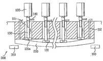
- FIG. 3illustrates a structure for holding substrates within a substrate bonding apparatus used in fabricating LCD devices according to principles of the present invention.
- a structure for holding substrates within a substrate bonding apparatus used in fabricating LCD devicesmay, for example, include an upper stage 110 , a lower stage 120 , suction force applying means, a vacuum pump 140 , and sensing means 150 for measuring a distance between a contact surface of the upper stage 110 and first substrate 210 and a contact surface of the lower stage 120 and the second substrate 220 .
- the upper and lower stages 110 and 120may hold first and second substrates 210 and 220 , respectively, by transmitting suction forces to operably proximate portions of substrates 210 and 220 , respectively.
- a plurality of passages 111 and 121may be formed within stages 110 and 120 , respectively, wherein each of the passages 111 and 121 intersect with the contact surfaces of the upper and lower stages 110 and 120 , respectively.
- the passagesmay be, for example, cylindrically shaped.
- the suction force applying meansmay be arranged within each of the plurality of passages 111 and 121 and may hold substrates 210 and 220 , respectively, to upper and lower stages 110 and 120 , respectively, by transmitting a vacuum suction force to operably proximate portions of the substrates 210 and 220 , respectively.
- the suction force applying meansmay, for example, include a plurality of pads 131 , a plurality of moving pipes 132 , and a plurality of driving parts 133 .
- each of the plurality of pads 131may include at least one vacuum hole 131 a for transmitting a suction force to the operably proximate portions of the substrates 210 and 220 .
- each of the plurality of moving pipes 132may be in fluid communication with each vacuum hole 131 a within a pad 131 .
- each of the plurality of moving pipes 132may raise or lower a respective pad 131 into and out of a respective one of the plurality of passages 111 and 121 . Further, each of the plurality of moving pipes 132 may be in fluid communication with the vacuum pump 140 , wherein the vacuum pump may generate the aforementioned suction force. In still another aspect of the present invention, each of the plurality of driving parts 133 may be connected to a respective one of the moving pipes 132 for independently raising or lowering each respective moving pipe 132 within its respective passage 111 or 121 .
- each moving pipe 132may include a first end and a second end, wherein the first end may be in fluid communication with each vacuum hole 131 a within its respective pad 131 , and wherein the second end may be arranged within each passage 111 and 121 . Further, the second end may be in fluid communication with a connection pipe 141 of the vacuum pump 140 . In yet another aspect of the present invention, the second end of each moving pipe 132 may be moved (e.g., raised and/or lowered) within a respective passage 111 or 121 by the driving part 133 .
- the driving part 133may, for example, be provided as an actuator wherein the moving pipe 132 is an axis.
- the driving part 133may, for example, be provided as a step motor or a linear motor, wherein the moving pipe 132 is the axis. It is appreciated, however, that the driving part 133 may be provided as substantially any mechanism suitable for moving the moving pipe 132 .
- the vacuum pump 140may generate a suction force by pumping. The generated suction force may be transmitted to each pad 131 via a respective moving pipe 132 .
- the sensing means 150may measure a distance between a contact surface of the upper stage 110 and first substrate 210 and a contact surface of the lower stage 120 and second substrate 220 .
- the sensing means 150may be provided as an interval check sensor.
- a plurality of vacuum holes 112 and 122may be arranged within stages 110 and 120 , respectively, for transmitting the generated suction force generated by the vacuum pump 140 from the contact surface of the upper and lower stages 110 and 120 , respectively, to operably proximate portions of the substrates 210 and 220 , respectively (e.g., peripheral edges).
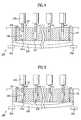
- FIGS. 4 to 7illustrate a method by which substrates are held within a substrate bonding apparatus used in fabricating LCD devices according to principles of the present invention
- a loader 300may be used to arrange a first substrate 210 proximate a contact surface of the upper stage 110 .
- sealant materialmay be arranged on a surface of the first substrate 210 opposite the contact surface of the first substrate 210 .
- the loader 300may be provided with at least one finger 310 to minimize the degree to which portions of the first substrate 210 sag with respect to the contact surface of the upper stage 110 . As shown in FIG. 4 , however, portions of the first substrate 210 unsupported by fingers 310 , may still sag with respect to the contact surface of the upper stage 210 .
- the vacuum pump 140may be activated to generate a suction force that is transmitted by the vacuum holes 112 formed in the upper stage 110 . Accordingly, the vacuum holes 112 transmit the generated suction force from the contact surface of the upper stage 110 to hold the operably proximate portions of the first substrate 210 against the contact surface of the upper stage 110 , as shown in FIG. 5 .
- portions of the first substrate 210may not be operably proximate to the contact surface of the upper stage 110 (i.e., the first substrate 210 may sag with respect to the contact surface of the upper stage 110 ) and may therefore not be affected by the suction force transmitted by the vacuum holes 131 a.
- each driving part 133may be independently driven to lower respective ones of the moving pipes 132 a predetermined distance from the contact surface of the upper stage 110 .
- respective ones of the vacuum holes 131 amay be arranged operably proximate the sagging portions of first substrate 210 .
- each moving pipe 132may be lowered a predetermined distance in accordance with an output of the sensing means 150 .
- the suction force, generated by the vacuum pump 140may be effectively transmitted from the vacuum hole 131 a of each pad 131 through each moving pipe 132 to the sagging portions of the first substrate 210 .
- portions of the first substrate 210 previously found sagging with respect to the contact surface of the upper stage 210may be held to the projected pads 131 by the transmitted suction force.
- each driving part 133may be independently driven again to raise respective ones of the moving pipes 132 by a predetermined distance.
- the moving pipes 132may be raised such that a lower surface of each of the pads 131 is substantially flush with the contact surface of the upper stage 110 .
- the moving pipes 132may be raised such that the first substrate 210 is held substantially parallel to the contact surface of the upper stage 110 , as shown in FIG. 7 .
- the second substrate 220may be held to a contact surface of the lower stage 120 .
- the second substrate 220may be held by the lower stage 120 by, for example, providing the second substrate 220 on the loader 300 , arranging the loader 300 between the upper and lower stages 110 and 120 , respectively, and arranging the second substrate 220 proximate the contact surface of the lower stage 120 .
- the process for holding the proximately arranged second substrate 220 to the lower stage 120may be performed by essentially the same method as described above for holding the first substrate 210 to the upper stage 110 and, therefore, a detailed description of such a holding process will be omitted.
- the method by which the second substrate 220 is held to the lower stage 120may be different from the process described above for holding the first substrate 210 to the upper stage 110 .
- the first and second substrates 210 and 220may be bonded together.
- the structure for holding substrates within a substrate bonding apparatus used in fabricating LCD devicesis beneficial because substrates may be substantially prevented from sagging without transmitting excessively large, and damaging, suction forces.
- suction forcesmay be effectively transmitted by the stage to operably proximate portions of a substrate.
- some portions of the substratee.g., peripheral portions
- other portions of the substratee.g., interior portions
- the substratemay appear to sag with respect to the contact surface of the stage.
- pads of the suction force applying meansmay be moved operably proximate potions of the substrate that are sagging to effectively transmit suction forces. Once suction forces have been effectively transmitted to the sagging portions of the substrate, the pads may be moved such that the substrate is held substantially parallel to the contact surface of the stage.
Landscapes
- Physics & Mathematics (AREA)
- Nonlinear Science (AREA)
- Chemical & Material Sciences (AREA)
- Crystallography & Structural Chemistry (AREA)
- General Physics & Mathematics (AREA)
- Optics & Photonics (AREA)
- Mathematical Physics (AREA)
- Liquid Crystal (AREA)
- Devices For Indicating Variable Information By Combining Individual Elements (AREA)
Abstract
Description
Claims (11)
Priority Applications (1)
| Application Number | Priority Date | Filing Date | Title |
|---|---|---|---|
| US11/984,689US7836934B2 (en) | 2002-11-07 | 2007-11-20 | Structure for loading substrate in substrate bonding apparatus for fabricating liquid crystal display device |
Applications Claiming Priority (5)
| Application Number | Priority Date | Filing Date | Title |
|---|---|---|---|
| KR10-2002-0068822 | 2002-11-07 | ||
| KRP2002-68822 | 2002-11-07 | ||
| KR10-2002-0068822AKR100493384B1 (en) | 2002-11-07 | 2002-11-07 | structure for loading of substrate in substrate bonding device for manucturing a liquid crystal display device |
| US10/700,475US7314535B2 (en) | 2002-11-07 | 2003-11-05 | Structure for loading substrate in substrate bonding apparatus for fabricating liquid crystal display device |
| US11/984,689US7836934B2 (en) | 2002-11-07 | 2007-11-20 | Structure for loading substrate in substrate bonding apparatus for fabricating liquid crystal display device |
Related Parent Applications (1)
| Application Number | Title | Priority Date | Filing Date |
|---|---|---|---|
| US10/700,475DivisionUS7314535B2 (en) | 2002-11-07 | 2003-11-05 | Structure for loading substrate in substrate bonding apparatus for fabricating liquid crystal display device |
Publications (2)
| Publication Number | Publication Date |
|---|---|
| US20080099138A1 US20080099138A1 (en) | 2008-05-01 |
| US7836934B2true US7836934B2 (en) | 2010-11-23 |
Family
ID=32226249
Family Applications (2)
| Application Number | Title | Priority Date | Filing Date |
|---|---|---|---|
| US10/700,475Expired - LifetimeUS7314535B2 (en) | 2002-11-07 | 2003-11-05 | Structure for loading substrate in substrate bonding apparatus for fabricating liquid crystal display device |
| US11/984,689Expired - Fee RelatedUS7836934B2 (en) | 2002-11-07 | 2007-11-20 | Structure for loading substrate in substrate bonding apparatus for fabricating liquid crystal display device |
Family Applications Before (1)
| Application Number | Title | Priority Date | Filing Date |
|---|---|---|---|
| US10/700,475Expired - LifetimeUS7314535B2 (en) | 2002-11-07 | 2003-11-05 | Structure for loading substrate in substrate bonding apparatus for fabricating liquid crystal display device |
Country Status (2)
| Country | Link |
|---|---|
| US (2) | US7314535B2 (en) |
| KR (1) | KR100493384B1 (en) |
Cited By (2)
| Publication number | Priority date | Publication date | Assignee | Title |
|---|---|---|---|---|
| US10301883B2 (en) | 2017-05-03 | 2019-05-28 | Coil Solutions, Inc. | Bit jet enhancement tool |
| US10502014B2 (en) | 2017-05-03 | 2019-12-10 | Coil Solutions, Inc. | Extended reach tool |
Families Citing this family (26)
| Publication number | Priority date | Publication date | Assignee | Title |
|---|---|---|---|---|
| JP3693972B2 (en)* | 2002-03-19 | 2005-09-14 | 富士通株式会社 | Bonded substrate manufacturing apparatus and substrate bonding method |
| JP4213610B2 (en)* | 2004-03-15 | 2009-01-21 | 富士通株式会社 | Bonded board manufacturing equipment |
| US7637263B2 (en)* | 2004-05-07 | 2009-12-29 | Ardica Technologies, Inc. | Method of controlling body temperature with an electrochemical device while providing on-demand power to an electrical device |
| JP4482395B2 (en)* | 2004-08-03 | 2010-06-16 | 芝浦メカトロニクス株式会社 | Substrate bonding method and bonding apparatus |
| JP2006201330A (en)* | 2005-01-19 | 2006-08-03 | Fujitsu Ltd | Bonded substrate manufacturing apparatus and bonded substrate manufacturing method |
| US8187758B2 (en)* | 2005-08-11 | 2012-05-29 | Ardica Technologies Inc. | Fuel cell apparatus with a split pump |
| US20070036711A1 (en)* | 2005-08-11 | 2007-02-15 | Ardica Technologies Inc. | Hydrogen generator |
| KR100760561B1 (en)* | 2005-11-15 | 2007-09-20 | 주식회사 에이디엠 | Roll device |
| HU227011B1 (en)* | 2006-04-20 | 2010-04-28 | Mirrotron Kft | Method of manufacturing multi layers neutron guides |
| US7790507B2 (en)* | 2007-03-24 | 2010-09-07 | Texas Instruments Incorporated | Semiconductor die collet and method |
| JP2011511416A (en)* | 2008-01-29 | 2011-04-07 | アーディカ テクノロジーズ インコーポレイテッド | System for purging non-fuel material from a fuel cell anode |
| KR100962953B1 (en) | 2008-04-23 | 2010-06-10 | 로체 시스템즈(주) | Glass substrate transfer robot |
| US8469074B2 (en)* | 2008-05-19 | 2013-06-25 | Kwangwoo Michael Ko | Pressure control mechanism for adhesive thermal compression bonding machines |
| ITMO20080200A1 (en)* | 2008-07-23 | 2010-01-24 | Aper S R L | MACHINE FOR GLUE SHEETS IN POROUS MATERIAL |
| US20100053852A1 (en)* | 2008-09-02 | 2010-03-04 | Cheng Uei Precision Industry Co., Ltd. | Display Device |
| KR101007996B1 (en)* | 2008-12-12 | 2011-01-14 | 엘아이지에이디피 주식회사 | Board Bonding Device |
| US20110020215A1 (en)* | 2009-07-23 | 2011-01-27 | Ryu Wonhyoung | Chemical hydride formulation and system design for controlled generation of hydrogen |
| US20110053016A1 (en)* | 2009-08-25 | 2011-03-03 | Daniel Braithwaite | Method for Manufacturing and Distributing Hydrogen Storage Compositions |
| KR101036797B1 (en)* | 2011-03-31 | 2011-05-25 | 한국뉴매틱(주) | Vacuum gripper device |
| KR101859964B1 (en)* | 2011-06-29 | 2018-05-24 | 삼성디스플레이 주식회사 | Apparatus of sealing substrate and method of sealing substrate using the same |
| WO2013023708A1 (en)* | 2011-08-12 | 2013-02-21 | Ev Group E. Thallner Gmbh | Apparatus and method for bonding substrates |
| KR101973779B1 (en)* | 2012-11-19 | 2019-04-30 | 삼성디스플레이 주식회사 | Method and device of manufacturing flexible display device |
| US10121760B2 (en) | 2013-11-01 | 2018-11-06 | Nikon Corporation | Wafer bonding system and method |
| CN103755161B (en) | 2013-12-31 | 2016-03-30 | 深圳市华星光电技术有限公司 | The rigging machine mounting structure of sheet material mounting block and top board, rigging machine |
| US12105368B2 (en)* | 2019-07-29 | 2024-10-01 | Lg Electronics Inc. | Curved display device manufacturing method |
| CN112828560A (en)* | 2021-02-03 | 2021-05-25 | 广州曼越科技信息有限公司 | Shell installation equipment for production and processing of instruments and meters |
Citations (97)
| Publication number | Priority date | Publication date | Assignee | Title |
|---|---|---|---|---|
| US3498663A (en) | 1967-11-29 | 1970-03-03 | Home Comfort Products Co | Adjustable vacuum platen |
| JPS5165656A (en) | 1974-12-04 | 1976-06-07 | Shinshu Seiki Kk | |
| US3978580A (en) | 1973-06-28 | 1976-09-07 | Hughes Aircraft Company | Method of fabricating a liquid crystal display |
| US4094058A (en) | 1976-07-23 | 1978-06-13 | Omron Tateisi Electronics Co. | Method of manufacture of liquid crystal displays |
| JPS5738414A (en) | 1980-08-20 | 1982-03-03 | Showa Denko Kk | Spacer for display panel |
| JPS5788428A (en) | 1980-11-20 | 1982-06-02 | Ricoh Elemex Corp | Manufacture of liquid crystal display body device |
| JPS5827126A (en) | 1981-08-11 | 1983-02-17 | Nec Corp | Production of liquid crystal display panel |
| JPS5957221A (en) | 1982-09-28 | 1984-04-02 | Asahi Glass Co Ltd | Production of display element |
| JPS59195222A (en) | 1983-04-19 | 1984-11-06 | Matsushita Electric Ind Co Ltd | Manufacture of liquid-crystal panel |
| JPS60111221A (en) | 1983-11-19 | 1985-06-17 | Nippon Denso Co Ltd | Method and device for charging liquid crystal |
| JPS60164723A (en) | 1984-02-07 | 1985-08-27 | Seiko Instr & Electronics Ltd | Liquid crystal display device |
| JPS60217343A (en) | 1984-04-13 | 1985-10-30 | Matsushita Electric Ind Co Ltd | Liquid crystal display device and its preparation |
| JPS617822A (en) | 1984-06-22 | 1986-01-14 | Canon Inc | Production of liquid crystal element |
| JPS6155625A (en) | 1984-08-24 | 1986-03-20 | Nippon Denso Co Ltd | Manufacture of liquid crystal element |
| JPS6254229A (en) | 1985-07-15 | 1987-03-09 | Semiconductor Energy Lab Co Ltd | Manufacturing method for liquid crystal display |
| JPS6254225A (en) | 1985-07-15 | 1987-03-09 | Semiconductor Energy Lab Co Ltd | Manufacturing method for liquid crystal display |
| JPS6254228A (en) | 1985-07-15 | 1987-03-09 | Semiconductor Energy Lab Co Ltd | Manufacturing method for liquid crystal display |
| US4653864A (en) | 1986-02-26 | 1987-03-31 | Ovonic Imaging Systems, Inc. | Liquid crystal matrix display having improved spacers and method of making same |
| JPS6289025A (en) | 1985-10-15 | 1987-04-23 | Matsushita Electric Ind Co Ltd | Manufacturing method of liquid crystal display panel |
| JPS6290622A (en) | 1985-10-17 | 1987-04-25 | Seiko Epson Corp | liquid crystal display device |
| US4691995A (en) | 1985-07-15 | 1987-09-08 | Semiconductor Energy Laboratory Co., Ltd. | Liquid crystal filling device |
| JPS62205319A (en) | 1986-03-06 | 1987-09-09 | Canon Inc | Ferroelectric liquid crystal element |
| JPS63110425A (en) | 1986-10-29 | 1988-05-14 | Toppan Printing Co Ltd | Cell for liquid crystal filling |
| JPS63109413A (en) | 1986-10-27 | 1988-05-14 | Fujitsu Ltd | Manufacturing method of LCD display |
| JPS63128315A (en) | 1986-11-19 | 1988-05-31 | Victor Co Of Japan Ltd | Liquid crystal display element |
| US4775225A (en) | 1985-05-16 | 1988-10-04 | Canon Kabushiki Kaisha | Liquid crystal device having pillar spacers with small base periphery width in direction perpendicular to orientation treatment |
| JPS63311233A (en) | 1987-06-12 | 1988-12-20 | Toyota Motor Corp | lcd cell |
| JPH039549A (en) | 1989-05-16 | 1991-01-17 | Motorola Inc | Composite integrated storage device |
| JPH0536426A (en) | 1991-07-31 | 1993-02-12 | Mitsubishi Heavy Ind Ltd | Solid electrolytic fuel cell |
| JPH0536425A (en) | 1991-02-12 | 1993-02-12 | Tokyo Electric Power Co Inc:The | Alloy separator for solid oxide fuel cell and method for producing the same |
| JPH05107533A (en) | 1991-10-16 | 1993-04-30 | Shinetsu Eng Kk | Method for laminating glass substrate for liquid crystal display panel and laminating apparatus therefor |
| JPH05127179A (en) | 1991-11-01 | 1993-05-25 | Ricoh Co Ltd | Production of liquid crystal display element |
| JPH05154923A (en) | 1991-12-06 | 1993-06-22 | Hitachi Ltd | Substrate assembling device |
| US5247377A (en) | 1988-07-23 | 1993-09-21 | Rohm Gmbh Chemische Fabrik | Process for producing anisotropic liquid crystal layers on a substrate |
| JPH05265011A (en) | 1992-03-19 | 1993-10-15 | Seiko Instr Inc | Production of liquid crystal display element |
| JPH05281557A (en) | 1992-04-01 | 1993-10-29 | Matsushita Electric Ind Co Ltd | Liquid crystal panel manufacturing method |
| JPH05281562A (en) | 1992-04-01 | 1993-10-29 | Matsushita Electric Ind Co Ltd | Manufacture of liquid crystal panel |
| US5263888A (en) | 1992-02-20 | 1993-11-23 | Matsushita Electric Industrial Co., Ltd. | Method of manufacture of liquid crystal display panel |
| JPH0618829A (en) | 1992-06-30 | 1994-01-28 | Shinetsu Eng Kk | Device for laminating glass substrates for liquid crystal display boards |
| JPH0651256A (en) | 1992-07-30 | 1994-02-25 | Matsushita Electric Ind Co Ltd | Device for discharging liquid crystal |
| JPH0664229A (en) | 1992-08-24 | 1994-03-08 | Toshiba Corp | Optical printing head |
| JPH06148657A (en) | 1992-11-06 | 1994-05-27 | Matsushita Electric Ind Co Ltd | Method of manufacturing cell for liquid crystal display and manufacturing apparatus thereof |
| JPH06160871A (en) | 1992-11-26 | 1994-06-07 | Matsushita Electric Ind Co Ltd | Liquid crystal display panel and manufacturing method thereof |
| JPH06194637A (en) | 1992-12-24 | 1994-07-15 | Shinetsu Eng Kk | Method for sticking glass substrate for liquid crystal display plate |
| JPH06235925A (en) | 1993-02-10 | 1994-08-23 | Matsushita Electric Ind Co Ltd | Manufacture of liquid crystal display element |
| JPH06265915A (en) | 1993-03-12 | 1994-09-22 | Matsushita Electric Ind Co Ltd | Discharge device for filling liquid crystal |
| JPH06313870A (en) | 1993-04-28 | 1994-11-08 | Hitachi Ltd | Substrate assembly device |
| US5379139A (en) | 1986-08-20 | 1995-01-03 | Semiconductor Energy Laboratory Co., Ltd. | Liquid crystal device and method for manufacturing same with spacers formed by photolithography |
| JPH0784268A (en) | 1993-09-13 | 1995-03-31 | Hitachi Ltd | Sealing agent drawing method |
| US5406989A (en) | 1993-10-12 | 1995-04-18 | Ayumi Industry Co., Ltd. | Method and dispenser for filling liquid crystal into LCD cell |
| JPH07128674A (en) | 1993-11-05 | 1995-05-19 | Matsushita Electric Ind Co Ltd | Liquid crystal display element manufacturing method |
| JPH07181507A (en) | 1993-12-21 | 1995-07-21 | Canon Inc | Liquid crystal display device and information transmission device including the liquid crystal display device |
| JPH07275770A (en) | 1994-04-06 | 1995-10-24 | Hitachi Techno Eng Co Ltd | Paste applicator |
| JPH07275771A (en) | 1994-04-11 | 1995-10-24 | Hitachi Techno Eng Co Ltd | Paste applicator |
| US5499128A (en) | 1993-03-15 | 1996-03-12 | Kabushiki Kaisha Toshiba | Liquid crystal display device with acrylic polymer spacers and method of manufacturing the same |
| JPH0876133A (en) | 1994-09-02 | 1996-03-22 | Shinetsu Eng Kk | Surface plate structure in a bonding apparatus for glass substrates for liquid crystal display boards |
| JPH0895066A (en) | 1994-09-27 | 1996-04-12 | Matsushita Electric Ind Co Ltd | Method and apparatus for manufacturing liquid crystal element |
| US5507323A (en) | 1993-10-12 | 1996-04-16 | Fujitsu Limited | Method and dispenser for filling liquid crystal into LCD cell |
| JPH08101395A (en) | 1994-09-30 | 1996-04-16 | Matsushita Electric Ind Co Ltd | Liquid crystal display element manufacturing method |
| JPH08106101A (en) | 1994-10-06 | 1996-04-23 | Fujitsu Ltd | Liquid crystal display panel manufacturing method |
| JPH08110504A (en) | 1994-10-13 | 1996-04-30 | Shinetsu Eng Kk | Glass substrate heating device for liquid crystal display panel |
| JPH08136937A (en) | 1994-11-09 | 1996-05-31 | Shinetsu Eng Kk | Method and apparatus for pressurizing and heating glass substrate for liquid crystal display panel |
| JPH08171094A (en) | 1994-12-19 | 1996-07-02 | Nippon Soken Inc | Liquid crystal injecting method and liquid crystal injecting device to liquid crystal display device |
| JPH08173874A (en) | 1994-12-26 | 1996-07-09 | Hitachi Techno Eng Co Ltd | Paste applicator |
| JPH08190099A (en) | 1995-01-11 | 1996-07-23 | Fujitsu Ltd | Liquid crystal display device manufacturing method and liquid crystal display device manufacturing apparatus |
| US5539545A (en) | 1993-05-18 | 1996-07-23 | Semiconductor Energy Laboratory Co., Ltd. | Method of making LCD in which resin columns are cured and the liquid crystal is reoriented |
| US5548429A (en) | 1993-06-14 | 1996-08-20 | Canon Kabushiki Kaisha | Process for producing liquid crystal device whereby curing the sealant takes place after pre-baking the substrates |
| JPH08240807A (en) | 1995-03-06 | 1996-09-17 | Fujitsu Ltd | Liquid crystal display panel sealing method |
| JPH091026A (en) | 1995-06-23 | 1997-01-07 | Hitachi Techno Eng Co Ltd | Paste applicator |
| JPH095762A (en) | 1995-06-20 | 1997-01-10 | Matsushita Electric Ind Co Ltd | Liquid crystal panel manufacturing method |
| JPH0926578A (en) | 1995-07-10 | 1997-01-28 | Fujitsu Ltd | Liquid crystal display panel and method of manufacturing the same |
| JPH0961829A (en) | 1995-08-21 | 1997-03-07 | Matsushita Electric Ind Co Ltd | Liquid crystal display element manufacturing method |
| JPH0973075A (en) | 1995-09-05 | 1997-03-18 | Matsushita Electric Ind Co Ltd | Liquid crystal display element manufacturing method and liquid crystal display element manufacturing apparatus |
| US5642214A (en) | 1991-07-19 | 1997-06-24 | Sharp Kabushiki Kaisha | Optical modulating element and electronic apparatus using it |
| JPH09311340A (en) | 1996-05-21 | 1997-12-02 | Matsushita Electric Ind Co Ltd | Liquid crystal display manufacturing method |
| US5742370A (en) | 1996-09-12 | 1998-04-21 | Korea Institute Of Science And Technology | Fabrication method for liquid crystal alignment layer by magnetic field treatment |
| US5757451A (en) | 1995-09-08 | 1998-05-26 | Kabushiki Kaisha Toshiba | Liquid crystal display device spacers formed from stacked color layers |
| US5805330A (en)* | 1996-03-15 | 1998-09-08 | Gentex Corporation | Electro-optic window incorporating a discrete photovoltaic device |
| US5852484A (en) | 1994-09-26 | 1998-12-22 | Matsushita Electric Industrial Co., Ltd. | Liquid crystal display panel and method and device for manufacturing the same |
| US5861932A (en) | 1997-03-31 | 1999-01-19 | Denso Corporation | Liquid crystal cell and its manufacturing method |
| US5875922A (en) | 1997-10-10 | 1999-03-02 | Nordson Corporation | Apparatus for dispensing an adhesive |
| US5952676A (en) | 1986-08-20 | 1999-09-14 | Semiconductor Energy Laboratory Co., Ltd. | Liquid crystal device and method for manufacturing same with spacers formed by photolithography |
| US5956112A (en) | 1995-10-02 | 1999-09-21 | Sharp Kabushiki Kaisha | Liquid crystal display device and method for manufacturing the same |
| US6001203A (en) | 1995-03-01 | 1999-12-14 | Matsushita Electric Industrial Co., Ltd. | Production process of liquid crystal display panel, seal material for liquid crystal cell and liquid crystal display |
| US6011609A (en) | 1996-10-05 | 2000-01-04 | Samsung Electronics Co., Ltd. | Method of manufacturing LCD by dropping liquid crystals on a substrate and then pressing the substrates |
| US6016181A (en) | 1996-11-07 | 2000-01-18 | Sharp Kabushiki Kaisha | Liquid crystal device having column spacers with portion on each of the spacers for reflecting or absorbing visible light and method for fabricating the same |
| US6016178A (en) | 1996-09-13 | 2000-01-18 | Sony Corporation | Reflective guest-host liquid-crystal display device |
| US6055035A (en) | 1998-05-11 | 2000-04-25 | International Business Machines Corporation | Method and apparatus for filling liquid crystal display (LCD) panels |
| EP1003066A1 (en) | 1998-11-16 | 2000-05-24 | Matsushita Electric Industrial Co., Ltd. | Method of manufacturing liquid crystal display devices |
| US6163357A (en) | 1996-09-26 | 2000-12-19 | Kabushiki Kaisha Toshiba | Liquid crystal display device having the driving circuit disposed in the seal area, with different spacer density in driving circuit area than display area |
| US6219126B1 (en) | 1998-11-20 | 2001-04-17 | International Business Machines Corporation | Panel assembly for liquid crystal displays having a barrier fillet and an adhesive fillet in the periphery |
| US6226067B1 (en) | 1997-10-03 | 2001-05-01 | Minolta Co., Ltd. | Liquid crystal device having spacers and manufacturing method thereof |
| US6236445B1 (en) | 1996-02-22 | 2001-05-22 | Hughes Electronics Corporation | Method for making topographic projections |
| US6304306B1 (en) | 1995-02-17 | 2001-10-16 | Sharp Kabushiki Kaisha | Liquid crystal display device and method for producing the same |
| US6337730B1 (en) | 1998-06-02 | 2002-01-08 | Denso Corporation | Non-uniformly-rigid barrier wall spacers used to correct problems caused by thermal contraction of smectic liquid crystal material |
| US6414733B1 (en) | 1999-02-08 | 2002-07-02 | Dai Nippon Printing Co., Ltd. | Color liquid crystal display with a shielding member being arranged between sealing member and display zone |
| US6665043B1 (en) | 1999-08-31 | 2003-12-16 | Sharp Kabushiki Kaisha | Bonding method and bonding device of substrates and manufacturing method of a liquid crystal display device |
Family Cites Families (132)
| Publication number | Priority date | Publication date | Assignee | Title |
|---|---|---|---|---|
| US5407519A (en)* | 1993-07-07 | 1995-04-18 | Interserv Corp. | Apparatus for manufacturing liquid crystal display screens |
| JPH086036A (en)* | 1994-06-17 | 1996-01-12 | Seiwa Sangyo Kk | Pressurizing device of liquid crystal panel assembly |
| JP3139945B2 (en) | 1995-09-29 | 2001-03-05 | 日立テクノエンジニアリング株式会社 | Paste coating machine |
| JP3161296B2 (en) | 1995-09-05 | 2001-04-25 | 松下電器産業株式会社 | Manufacturing method of liquid crystal display element |
| JPH0990377A (en)* | 1995-09-22 | 1997-04-04 | Sintokogio Ltd | Producing device of liquid crystal panel |
| JP3658604B2 (en) | 1995-10-27 | 2005-06-08 | 富士通ディスプレイテクノロジーズ株式会社 | Manufacturing method of liquid crystal panel |
| JPH09230357A (en) | 1996-02-22 | 1997-09-05 | Canon Inc | Liquid crystal panel manufacturing method and liquid crystal cell used therefor |
| JP3790295B2 (en) | 1996-04-17 | 2006-06-28 | シャープ株式会社 | Manufacturing method of liquid crystal display panel |
| KR0133148Y1 (en)* | 1996-04-26 | 1999-03-20 | 김광호 | Glass substrate unloading apparatus of lcd |
| JPH10123537A (en) | 1996-10-15 | 1998-05-15 | Matsushita Electric Ind Co Ltd | Liquid crystal display device and method of manufacturing the same |
| JP3088960B2 (en) | 1996-10-22 | 2000-09-18 | 松下電器産業株式会社 | Manufacturing method of liquid crystal display element |
| JPH10142616A (en) | 1996-11-14 | 1998-05-29 | Ayumi Kogyo Kk | Liquid crystal injection method and liquid dispenser |
| JPH10177178A (en) | 1996-12-17 | 1998-06-30 | Matsushita Electric Ind Co Ltd | Manufacturing method of liquid crystal display element |
| JP3372799B2 (en) | 1996-12-17 | 2003-02-04 | 株式会社 日立インダストリイズ | Paste coating machine |
| JP3874871B2 (en) | 1997-02-10 | 2007-01-31 | シャープ株式会社 | Manufacturing method of liquid crystal display device |
| JP3773326B2 (en) | 1997-04-07 | 2006-05-10 | アユミ工業株式会社 | Liquid crystal injection method and dispenser used therefor |
| JPH10333157A (en) | 1997-06-03 | 1998-12-18 | Matsushita Electric Ind Co Ltd | Manufacturing method of liquid crystal display device |
| JPH10333159A (en) | 1997-06-03 | 1998-12-18 | Matsushita Electric Ind Co Ltd | Liquid crystal display |
| JPH1114953A (en) | 1997-06-20 | 1999-01-22 | Matsushita Electric Ind Co Ltd | Method of manufacturing multi-touch liquid crystal display panel and multi-touch liquid crystal display panel |
| JP3874895B2 (en) | 1997-07-23 | 2007-01-31 | シャープ株式会社 | Manufacturing method of liquid crystal display panel |
| JPH1164811A (en) | 1997-08-21 | 1999-03-05 | Matsushita Electric Ind Co Ltd | Method and apparatus for manufacturing liquid crystal display element |
| JPH11109388A (en) | 1997-10-03 | 1999-04-23 | Hitachi Ltd | Manufacturing method of liquid crystal display device |
| JPH11133438A (en) | 1997-10-24 | 1999-05-21 | Matsushita Electric Ind Co Ltd | Liquid crystal display device and its manufacturing method |
| JPH11142864A (en) | 1997-11-07 | 1999-05-28 | Matsushita Electric Ind Co Ltd | Manufacturing method of liquid crystal display device |
| JPH11174477A (en) | 1997-12-08 | 1999-07-02 | Matsushita Electric Ind Co Ltd | Manufacturing method of liquid crystal display device |
| JPH11264991A (en) | 1998-01-13 | 1999-09-28 | Matsushita Electric Ind Co Ltd | Manufacturing method of liquid crystal display element |
| JPH11212045A (en) | 1998-01-26 | 1999-08-06 | Matsushita Electric Ind Co Ltd | Liquid crystal panel manufacturing method |
| JPH11248930A (en) | 1998-03-06 | 1999-09-17 | Matsushita Electric Ind Co Ltd | Color filter substrate, method of manufacturing the color filter substrate, and liquid crystal display device using the color filter substrate |
| JP3492190B2 (en) | 1998-03-17 | 2004-02-03 | 株式会社 日立インダストリイズ | Paste application method and paste application machine |
| JPH11326922A (en) | 1998-05-14 | 1999-11-26 | Matsushita Electric Ind Co Ltd | Liquid crystal display panel manufacturing method |
| JPH11344714A (en) | 1998-06-02 | 1999-12-14 | Denso Corp | Liquid crystal cell |
| JP3148859B2 (en) | 1998-06-12 | 2001-03-26 | 松下電器産業株式会社 | Apparatus and method for assembling liquid crystal panel |
| JP2000029035A (en) | 1998-07-09 | 2000-01-28 | Minolta Co Ltd | Liquid crystal element and its manufacture |
| JP2000056311A (en) | 1998-08-03 | 2000-02-25 | Matsushita Electric Ind Co Ltd | Liquid crystal display |
| JP2000066165A (en) | 1998-08-20 | 2000-03-03 | Matsushita Electric Ind Co Ltd | Liquid crystal display panel manufacturing method |
| JP2934438B1 (en) | 1998-08-21 | 1999-08-16 | 信越エンジニアリング株式会社 | LCD panel manufacturing equipment |
| JP3520205B2 (en) | 1998-09-18 | 2004-04-19 | 株式会社 日立インダストリイズ | Paste application method and paste application machine |
| JP2000137235A (en) | 1998-11-02 | 2000-05-16 | Matsushita Electric Ind Co Ltd | Liquid crystal substrate bonding method |
| KR20000035302A (en) | 1998-11-09 | 2000-06-26 | 마츠시타 덴끼 산교 가부시키가이샤 | Manufacturing method and apparatus of liquid crystal display |
| JP2000193988A (en) | 1998-12-25 | 2000-07-14 | Fujitsu Ltd | Method and apparatus for manufacturing liquid crystal display panel |
| JP2000241824A (en) | 1999-02-18 | 2000-09-08 | Matsushita Electric Ind Co Ltd | Manufacturing method of liquid crystal display device |
| JP2000310784A (en) | 1999-02-22 | 2000-11-07 | Matsushita Electric Ind Co Ltd | Liquid crystal panel, color filter and method for producing them |
| JP3410983B2 (en) | 1999-03-30 | 2003-05-26 | 株式会社 日立インダストリイズ | Substrate assembly method and apparatus |
| JP3535044B2 (en) | 1999-06-18 | 2004-06-07 | 株式会社 日立インダストリイズ | Substrate assembling apparatus and method, and liquid crystal panel manufacturing method |
| JP2000292799A (en) | 1999-04-09 | 2000-10-20 | Matsushita Electric Ind Co Ltd | Liquid crystal display device and method of manufacturing the same |
| JP2000310759A (en) | 1999-04-28 | 2000-11-07 | Matsushita Electric Ind Co Ltd | Liquid crystal display device manufacturing apparatus and method |
| JP2001013506A (en) | 1999-04-30 | 2001-01-19 | Matsushita Electric Ind Co Ltd | Liquid crystal display device and method of manufacturing the same |
| JP2001222017A (en) | 1999-05-24 | 2001-08-17 | Fujitsu Ltd | Liquid crystal display device and method of manufacturing the same |
| JP2000338501A (en) | 1999-05-26 | 2000-12-08 | Matsushita Electric Ind Co Ltd | Liquid crystal display panel manufacturing method |
| JP3486862B2 (en) | 1999-06-21 | 2004-01-13 | 株式会社 日立インダストリイズ | Substrate assembly method and apparatus |
| JP2001033793A (en) | 1999-07-21 | 2001-02-09 | Matsushita Electric Ind Co Ltd | Liquid crystal display panel and method of manufacturing the same |
| JP3422291B2 (en) | 1999-08-03 | 2003-06-30 | 株式会社 日立インダストリイズ | How to assemble a liquid crystal substrate |
| JP2001051284A (en) | 1999-08-10 | 2001-02-23 | Matsushita Electric Ind Co Ltd | Liquid crystal display device manufacturing equipment |
| JP2001091727A (en) | 1999-09-27 | 2001-04-06 | Matsushita Electric Ind Co Ltd | Method for manufacturing color filter substrate, color filter substrate and liquid crystal display device |
| JP3580767B2 (en) | 1999-10-05 | 2004-10-27 | 松下電器産業株式会社 | Liquid crystal display panel, manufacturing method and driving method thereof |
| JP2001117105A (en) | 1999-10-18 | 2001-04-27 | Toshiba Corp | Manufacturing method of liquid crystal display device |
| JP2001117109A (en) | 1999-10-21 | 2001-04-27 | Matsushita Electric Ind Co Ltd | Manufacturing method of liquid crystal display device |
| JP3583326B2 (en) | 1999-11-01 | 2004-11-04 | 協立化学産業株式会社 | Sealant for dripping method of LCD panel |
| JP2001133799A (en) | 1999-11-05 | 2001-05-18 | Fujitsu Ltd | Manufacturing method of liquid crystal display device |
| JP3574865B2 (en) | 1999-11-08 | 2004-10-06 | 株式会社 日立インダストリイズ | Substrate assembly method and apparatus |
| JP2001142074A (en) | 1999-11-10 | 2001-05-25 | Hitachi Ltd | Liquid crystal display |
| JP2001147437A (en) | 1999-11-19 | 2001-05-29 | Nec Corp | Liquid crystal display panel and method of producing the same |
| JP2001154211A (en) | 1999-11-30 | 2001-06-08 | Hitachi Ltd | Liquid crystal panel and method of manufacturing the same |
| JP2001166310A (en) | 1999-12-08 | 2001-06-22 | Matsushita Electric Ind Co Ltd | Liquid crystal display panel manufacturing method |
| JP3641709B2 (en) | 1999-12-09 | 2005-04-27 | 株式会社 日立インダストリイズ | Substrate assembly method and apparatus |
| JP4132528B2 (en) | 2000-01-14 | 2008-08-13 | シャープ株式会社 | Manufacturing method of liquid crystal display device |
| JP2001209052A (en) | 2000-01-24 | 2001-08-03 | Matsushita Electric Ind Co Ltd | Liquid crystal display device and method of manufacturing the same |
| JP2001209057A (en) | 2000-01-26 | 2001-08-03 | Shinetsu Engineering Kk | LCD panel manufacturing equipment |
| JP2001209056A (en) | 2000-01-25 | 2001-08-03 | Shinetsu Engineering Kk | LCD panel manufacturing equipment |
| JP3662156B2 (en) | 2000-01-26 | 2005-06-22 | 信越エンジニアリング株式会社 | LCD panel manufacturing equipment |
| JP2001213516A (en)* | 2000-02-02 | 2001-08-07 | Seiko Epson Corp | Electro-optical panel transport device, transport method thereof, and electro-optical device manufacturing method |
| JP2001215459A (en) | 2000-02-02 | 2001-08-10 | Matsushita Electric Ind Co Ltd | Liquid crystal display device manufacturing equipment |
| JP2001235758A (en) | 2000-02-23 | 2001-08-31 | Fujitsu Ltd | Liquid crystal display panel and method of manufacturing the same |
| JP2001255542A (en) | 2000-03-14 | 2001-09-21 | Sharp Corp | Substrate bonding method and substrate bonding apparatus, and method and apparatus for manufacturing liquid crystal display element |
| JP2001264782A (en) | 2000-03-16 | 2001-09-26 | Ayumi Kogyo Kk | Filling method of mucous material between flat panel substrates |
| JP2001272640A (en) | 2000-03-27 | 2001-10-05 | Fujitsu Ltd | Liquid crystal dropping device and liquid crystal dropping method |
| JP3678974B2 (en) | 2000-03-29 | 2005-08-03 | 富士通ディスプレイテクノロジーズ株式会社 | Manufacturing method of liquid crystal display device |
| JP2001281675A (en) | 2000-03-29 | 2001-10-10 | Matsushita Electric Ind Co Ltd | Manufacturing method of liquid crystal display device |
| JP3707990B2 (en) | 2000-03-30 | 2005-10-19 | 株式会社 日立インダストリイズ | Board assembly equipment |
| JP3492284B2 (en) | 2000-04-19 | 2004-02-03 | 株式会社 日立インダストリイズ | Substrate bonding device |
| JP2001330840A (en) | 2000-05-18 | 2001-11-30 | Toshiba Corp | Manufacturing method of liquid crystal display element |
| JP2001330837A (en) | 2000-05-19 | 2001-11-30 | Matsushita Electric Ind Co Ltd | Hermetic structure, method of manufacturing the same, liquid crystal display device using the same, and method of manufacturing the same |
| JP2001356354A (en) | 2000-06-13 | 2001-12-26 | Matsushita Electric Ind Co Ltd | Manufacturing method of liquid crystal display element |
| JP2002080321A (en) | 2000-06-20 | 2002-03-19 | Kyowa Hakko Kogyo Co Ltd | Cosmetic |
| JP2002014360A (en) | 2000-06-29 | 2002-01-18 | Matsushita Electric Ind Co Ltd | Method and apparatus for manufacturing liquid crystal panel |
| JP2002023176A (en) | 2000-07-05 | 2002-01-23 | Seiko Epson Corp | Liquid crystal injection device and liquid crystal injection method |
| JP2001066615A (en) | 2000-08-02 | 2001-03-16 | Matsushita Electric Ind Co Ltd | Manufacturing method of liquid crystal display device |
| JP2002049045A (en) | 2000-08-03 | 2002-02-15 | Nec Corp | Method for manufacturing liquid crystal display panel |
| JP3712927B2 (en) | 2000-09-04 | 2005-11-02 | 株式会社 日立インダストリイズ | Paste applicator |
| JP2002082340A (en) | 2000-09-08 | 2002-03-22 | Fuji Xerox Co Ltd | Method for manufacturing flat panel display |
| JP2002090760A (en) | 2000-09-12 | 2002-03-27 | Matsushita Electric Ind Co Ltd | Liquid crystal display panel manufacturing apparatus and method |
| JP2002090759A (en) | 2000-09-18 | 2002-03-27 | Sharp Corp | Apparatus and method for manufacturing liquid crystal display element |
| JP2002107740A (en) | 2000-09-28 | 2002-04-10 | Sharp Corp | Method and apparatus for manufacturing liquid crystal display panel |
| JP2002122872A (en) | 2000-10-12 | 2002-04-26 | Hitachi Ltd | Liquid crystal display device and manufacturing method thereof |
| JP4387052B2 (en) | 2000-10-13 | 2009-12-16 | シャープ株式会社 | Manufacturing method of liquid crystal display device |
| JP4841031B2 (en) | 2000-10-13 | 2011-12-21 | スタンレー電気株式会社 | Manufacturing method of liquid crystal device |
| JP3542956B2 (en) | 2000-10-30 | 2004-07-14 | 信越エンジニアリング株式会社 | LCD panel substrate bonding equipment |
| JP4330785B2 (en) | 2000-10-31 | 2009-09-16 | シャープ株式会社 | Liquid crystal display device manufacturing method and liquid crystal display device manufacturing apparatus |
| JP2002156518A (en) | 2000-11-16 | 2002-05-31 | Matsushita Electric Ind Co Ltd | Method for manufacturing color filter substrate |
| JP2002169167A (en) | 2000-12-05 | 2002-06-14 | Matsushita Electric Ind Co Ltd | Liquid crystal display device, manufacturing method thereof, and image display application device |
| JP2002169166A (en) | 2000-12-05 | 2002-06-14 | Matsushita Electric Ind Co Ltd | Liquid crystal display device, manufacturing method thereof, and image display application device |
| JP3281362B2 (en) | 2000-12-11 | 2002-05-13 | 富士通株式会社 | Liquid crystal display panel manufacturing method |
| JP2002182222A (en) | 2000-12-19 | 2002-06-26 | Matsushita Electric Ind Co Ltd | Liquid crystal panel manufacturing method |
| JP2002202512A (en) | 2000-12-28 | 2002-07-19 | Toshiba Corp | Liquid crystal display device and manufacturing method thereof |
| JP2002202514A (en) | 2000-12-28 | 2002-07-19 | Matsushita Electric Ind Co Ltd | Liquid crystal panel, method for manufacturing the same, and apparatus for manufacturing the same |
| JP2002214626A (en) | 2001-01-17 | 2002-07-31 | Toshiba Corp | Manufacturing method of liquid crystal display device and sealing material |
| JP3577545B2 (en) | 2001-02-06 | 2004-10-13 | 株式会社 日立インダストリイズ | Substrate bonding equipment |
| JP3577546B2 (en) | 2001-02-08 | 2004-10-13 | 株式会社 日立インダストリイズ | Substrate assembling method and assembling apparatus |
| JP2002236292A (en) | 2001-02-09 | 2002-08-23 | Matsushita Electric Ind Co Ltd | Liquid crystal panel manufacturing method and substrate bonding apparatus |
| JP2002258299A (en) | 2001-02-28 | 2002-09-11 | Matsushita Electric Ind Co Ltd | Method and apparatus for manufacturing liquid crystal display device and liquid crystal display device |
| JP4301741B2 (en) | 2001-03-16 | 2009-07-22 | 東芝松下ディスプレイテクノロジー株式会社 | Liquid crystal panel and manufacturing method thereof |
| JP2002277866A (en) | 2001-03-21 | 2002-09-25 | Matsushita Electric Ind Co Ltd | Liquid crystal panel manufacturing method |
| JP2002277865A (en) | 2001-03-21 | 2002-09-25 | Matsushita Electric Ind Co Ltd | Liquid crystal display device and manufacturing method thereof |
| JP2002287156A (en) | 2001-03-26 | 2002-10-03 | Matsushita Electric Ind Co Ltd | Method and apparatus for manufacturing liquid crystal panel |
| JP2002296605A (en) | 2001-03-30 | 2002-10-09 | Matsushita Electric Ind Co Ltd | Method of laminating liquid crystal substrates |
| JP2002311438A (en) | 2001-04-13 | 2002-10-23 | Matsushita Electric Ind Co Ltd | Method and apparatus for manufacturing liquid crystal display element |
| JP3458145B2 (en) | 2001-04-17 | 2003-10-20 | 株式会社 日立インダストリイズ | Substrate bonding method and apparatus |
| JP3557472B2 (en) | 2001-04-17 | 2004-08-25 | 株式会社 日立インダストリイズ | Liquid crystal substrate assembling method, assembling apparatus and liquid crystal supply apparatus |
| JP3487833B2 (en) | 2001-04-24 | 2004-01-19 | 株式会社 日立インダストリイズ | Substrate bonding method and bonding device |
| JP3411023B2 (en) | 2001-04-24 | 2003-05-26 | 株式会社 日立インダストリイズ | Board assembly equipment |
| JP4244529B2 (en) | 2001-04-25 | 2009-03-25 | 株式会社日立プラントテクノロジー | Method and apparatus for assembling liquid crystal substrate |
| JP2002333635A (en) | 2001-05-07 | 2002-11-22 | Matsushita Electric Ind Co Ltd | Liquid crystal display device, method of manufacturing the same, and device for manufacturing liquid crystal display device |
| JP2002333628A (en) | 2001-05-07 | 2002-11-22 | Matsushita Electric Ind Co Ltd | Liquid crystal display device, color filter substrate and array substrate |
| JP2002333843A (en) | 2001-05-10 | 2002-11-22 | Matsushita Electric Ind Co Ltd | Substrate bonding method and apparatus |
| JP2002341357A (en) | 2001-05-14 | 2002-11-27 | Matsushita Electric Ind Co Ltd | Manufacturing method and manufacturing apparatus for liquid crystal display device |
| JP2002341355A (en) | 2001-05-16 | 2002-11-27 | Matsushita Electric Ind Co Ltd | Method for manufacturing liquid crystal display device, array substrate, and liquid crystal display device |
| JP2002341356A (en) | 2001-05-18 | 2002-11-27 | Matsushita Electric Ind Co Ltd | Method and apparatus for forming gap in liquid crystal display panel |
| JP2002341358A (en) | 2001-05-18 | 2002-11-27 | Matsushita Electric Ind Co Ltd | Liquid crystal display panel manufacturing method |
| JP2002341359A (en) | 2001-05-18 | 2002-11-27 | Matsushita Electric Ind Co Ltd | Method and apparatus for manufacturing liquid crystal display element |
| JP2002341362A (en) | 2001-05-18 | 2002-11-27 | Matsushita Electric Ind Co Ltd | Liquid crystal display panel manufacturing method and liquid crystal panel manufacturing apparatus |
| JP2002341329A (en) | 2001-05-21 | 2002-11-27 | Matsushita Electric Ind Co Ltd | Liquid crystal display |
| JP4134907B2 (en)* | 2002-03-05 | 2008-08-20 | 株式会社日立プラントテクノロジー | Substrate holding method in vacuum, liquid crystal display device manufacturing method, substrate holding device, liquid crystal display device manufacturing apparatus |
- 2002
- 2002-11-07KRKR10-2002-0068822Apatent/KR100493384B1/ennot_activeExpired - Fee Related
- 2003
- 2003-11-05USUS10/700,475patent/US7314535B2/ennot_activeExpired - Lifetime
- 2007
- 2007-11-20USUS11/984,689patent/US7836934B2/ennot_activeExpired - Fee Related
Patent Citations (101)
| Publication number | Priority date | Publication date | Assignee | Title |
|---|---|---|---|---|
| US3498663A (en) | 1967-11-29 | 1970-03-03 | Home Comfort Products Co | Adjustable vacuum platen |
| US3978580A (en) | 1973-06-28 | 1976-09-07 | Hughes Aircraft Company | Method of fabricating a liquid crystal display |
| JPS5165656A (en) | 1974-12-04 | 1976-06-07 | Shinshu Seiki Kk | |
| US4094058A (en) | 1976-07-23 | 1978-06-13 | Omron Tateisi Electronics Co. | Method of manufacture of liquid crystal displays |
| JPS5738414A (en) | 1980-08-20 | 1982-03-03 | Showa Denko Kk | Spacer for display panel |
| JPS5788428A (en) | 1980-11-20 | 1982-06-02 | Ricoh Elemex Corp | Manufacture of liquid crystal display body device |
| JPS5827126A (en) | 1981-08-11 | 1983-02-17 | Nec Corp | Production of liquid crystal display panel |
| JPS5957221A (en) | 1982-09-28 | 1984-04-02 | Asahi Glass Co Ltd | Production of display element |
| JPS59195222A (en) | 1983-04-19 | 1984-11-06 | Matsushita Electric Ind Co Ltd | Manufacture of liquid-crystal panel |
| JPS60111221A (en) | 1983-11-19 | 1985-06-17 | Nippon Denso Co Ltd | Method and device for charging liquid crystal |
| JPS60164723A (en) | 1984-02-07 | 1985-08-27 | Seiko Instr & Electronics Ltd | Liquid crystal display device |
| JPS60217343A (en) | 1984-04-13 | 1985-10-30 | Matsushita Electric Ind Co Ltd | Liquid crystal display device and its preparation |
| JPS617822A (en) | 1984-06-22 | 1986-01-14 | Canon Inc | Production of liquid crystal element |
| JPS6155625A (en) | 1984-08-24 | 1986-03-20 | Nippon Denso Co Ltd | Manufacture of liquid crystal element |
| US4775225A (en) | 1985-05-16 | 1988-10-04 | Canon Kabushiki Kaisha | Liquid crystal device having pillar spacers with small base periphery width in direction perpendicular to orientation treatment |
| JPS6254229A (en) | 1985-07-15 | 1987-03-09 | Semiconductor Energy Lab Co Ltd | Manufacturing method for liquid crystal display |
| JPS6254228A (en) | 1985-07-15 | 1987-03-09 | Semiconductor Energy Lab Co Ltd | Manufacturing method for liquid crystal display |
| US4691995A (en) | 1985-07-15 | 1987-09-08 | Semiconductor Energy Laboratory Co., Ltd. | Liquid crystal filling device |
| JPS6254225A (en) | 1985-07-15 | 1987-03-09 | Semiconductor Energy Lab Co Ltd | Manufacturing method for liquid crystal display |
| JPS6289025A (en) | 1985-10-15 | 1987-04-23 | Matsushita Electric Ind Co Ltd | Manufacturing method of liquid crystal display panel |
| JPS6290622A (en) | 1985-10-17 | 1987-04-25 | Seiko Epson Corp | liquid crystal display device |
| US4653864A (en) | 1986-02-26 | 1987-03-31 | Ovonic Imaging Systems, Inc. | Liquid crystal matrix display having improved spacers and method of making same |
| JPS62205319A (en) | 1986-03-06 | 1987-09-09 | Canon Inc | Ferroelectric liquid crystal element |
| US5379139A (en) | 1986-08-20 | 1995-01-03 | Semiconductor Energy Laboratory Co., Ltd. | Liquid crystal device and method for manufacturing same with spacers formed by photolithography |
| US5952676A (en) | 1986-08-20 | 1999-09-14 | Semiconductor Energy Laboratory Co., Ltd. | Liquid crystal device and method for manufacturing same with spacers formed by photolithography |
| JPS63109413A (en) | 1986-10-27 | 1988-05-14 | Fujitsu Ltd | Manufacturing method of LCD display |
| JPS63110425A (en) | 1986-10-29 | 1988-05-14 | Toppan Printing Co Ltd | Cell for liquid crystal filling |
| JPS63128315A (en) | 1986-11-19 | 1988-05-31 | Victor Co Of Japan Ltd | Liquid crystal display element |
| JPS63311233A (en) | 1987-06-12 | 1988-12-20 | Toyota Motor Corp | lcd cell |
| US5247377A (en) | 1988-07-23 | 1993-09-21 | Rohm Gmbh Chemische Fabrik | Process for producing anisotropic liquid crystal layers on a substrate |
| JPH039549A (en) | 1989-05-16 | 1991-01-17 | Motorola Inc | Composite integrated storage device |
| JPH0536425A (en) | 1991-02-12 | 1993-02-12 | Tokyo Electric Power Co Inc:The | Alloy separator for solid oxide fuel cell and method for producing the same |
| US5642214A (en) | 1991-07-19 | 1997-06-24 | Sharp Kabushiki Kaisha | Optical modulating element and electronic apparatus using it |
| JPH0536426A (en) | 1991-07-31 | 1993-02-12 | Mitsubishi Heavy Ind Ltd | Solid electrolytic fuel cell |
| JPH05107533A (en) | 1991-10-16 | 1993-04-30 | Shinetsu Eng Kk | Method for laminating glass substrate for liquid crystal display panel and laminating apparatus therefor |
| JPH05127179A (en) | 1991-11-01 | 1993-05-25 | Ricoh Co Ltd | Production of liquid crystal display element |
| JPH05154923A (en) | 1991-12-06 | 1993-06-22 | Hitachi Ltd | Substrate assembling device |
| US5263888A (en) | 1992-02-20 | 1993-11-23 | Matsushita Electric Industrial Co., Ltd. | Method of manufacture of liquid crystal display panel |
| JPH05265011A (en) | 1992-03-19 | 1993-10-15 | Seiko Instr Inc | Production of liquid crystal display element |
| JPH05281557A (en) | 1992-04-01 | 1993-10-29 | Matsushita Electric Ind Co Ltd | Liquid crystal panel manufacturing method |
| JPH05281562A (en) | 1992-04-01 | 1993-10-29 | Matsushita Electric Ind Co Ltd | Manufacture of liquid crystal panel |
| US5511591A (en) | 1992-04-13 | 1996-04-30 | Fujitsu Limited | Method and dispenser for filling liquid crystal into LCD cell |
| JPH0618829A (en) | 1992-06-30 | 1994-01-28 | Shinetsu Eng Kk | Device for laminating glass substrates for liquid crystal display boards |
| JPH0651256A (en) | 1992-07-30 | 1994-02-25 | Matsushita Electric Ind Co Ltd | Device for discharging liquid crystal |
| JPH0664229A (en) | 1992-08-24 | 1994-03-08 | Toshiba Corp | Optical printing head |
| JPH06148657A (en) | 1992-11-06 | 1994-05-27 | Matsushita Electric Ind Co Ltd | Method of manufacturing cell for liquid crystal display and manufacturing apparatus thereof |
| JPH06160871A (en) | 1992-11-26 | 1994-06-07 | Matsushita Electric Ind Co Ltd | Liquid crystal display panel and manufacturing method thereof |
| JPH06194637A (en) | 1992-12-24 | 1994-07-15 | Shinetsu Eng Kk | Method for sticking glass substrate for liquid crystal display plate |
| JPH06235925A (en) | 1993-02-10 | 1994-08-23 | Matsushita Electric Ind Co Ltd | Manufacture of liquid crystal display element |
| JPH06265915A (en) | 1993-03-12 | 1994-09-22 | Matsushita Electric Ind Co Ltd | Discharge device for filling liquid crystal |
| US5499128A (en) | 1993-03-15 | 1996-03-12 | Kabushiki Kaisha Toshiba | Liquid crystal display device with acrylic polymer spacers and method of manufacturing the same |
| JPH06313870A (en) | 1993-04-28 | 1994-11-08 | Hitachi Ltd | Substrate assembly device |
| US5680189A (en) | 1993-05-18 | 1997-10-21 | Semiconductor Energy Laboratory Co., Ltd. | LCD columnar spacers made of a hydrophilic resin and LCD orientation film having a certain surface tension or alignment capability |
| US5539545A (en) | 1993-05-18 | 1996-07-23 | Semiconductor Energy Laboratory Co., Ltd. | Method of making LCD in which resin columns are cured and the liquid crystal is reoriented |
| US5548429A (en) | 1993-06-14 | 1996-08-20 | Canon Kabushiki Kaisha | Process for producing liquid crystal device whereby curing the sealant takes place after pre-baking the substrates |
| JPH0784268A (en) | 1993-09-13 | 1995-03-31 | Hitachi Ltd | Sealing agent drawing method |
| US5406989A (en) | 1993-10-12 | 1995-04-18 | Ayumi Industry Co., Ltd. | Method and dispenser for filling liquid crystal into LCD cell |
| US5507323A (en) | 1993-10-12 | 1996-04-16 | Fujitsu Limited | Method and dispenser for filling liquid crystal into LCD cell |
| JPH07128674A (en) | 1993-11-05 | 1995-05-19 | Matsushita Electric Ind Co Ltd | Liquid crystal display element manufacturing method |
| JPH07181507A (en) | 1993-12-21 | 1995-07-21 | Canon Inc | Liquid crystal display device and information transmission device including the liquid crystal display device |
| JPH07275770A (en) | 1994-04-06 | 1995-10-24 | Hitachi Techno Eng Co Ltd | Paste applicator |
| JPH07275771A (en) | 1994-04-11 | 1995-10-24 | Hitachi Techno Eng Co Ltd | Paste applicator |
| JPH0876133A (en) | 1994-09-02 | 1996-03-22 | Shinetsu Eng Kk | Surface plate structure in a bonding apparatus for glass substrates for liquid crystal display boards |
| US5854664A (en) | 1994-09-26 | 1998-12-29 | Matsushita Electric Industrial Co., Ltd. | Liquid crystal display panel and method and device for manufacturing the same |
| US5852484A (en) | 1994-09-26 | 1998-12-22 | Matsushita Electric Industrial Co., Ltd. | Liquid crystal display panel and method and device for manufacturing the same |
| JPH0895066A (en) | 1994-09-27 | 1996-04-12 | Matsushita Electric Ind Co Ltd | Method and apparatus for manufacturing liquid crystal element |
| JPH08101395A (en) | 1994-09-30 | 1996-04-16 | Matsushita Electric Ind Co Ltd | Liquid crystal display element manufacturing method |
| JPH08106101A (en) | 1994-10-06 | 1996-04-23 | Fujitsu Ltd | Liquid crystal display panel manufacturing method |
| JPH08110504A (en) | 1994-10-13 | 1996-04-30 | Shinetsu Eng Kk | Glass substrate heating device for liquid crystal display panel |
| JPH08136937A (en) | 1994-11-09 | 1996-05-31 | Shinetsu Eng Kk | Method and apparatus for pressurizing and heating glass substrate for liquid crystal display panel |
| JPH08171094A (en) | 1994-12-19 | 1996-07-02 | Nippon Soken Inc | Liquid crystal injecting method and liquid crystal injecting device to liquid crystal display device |
| JPH08173874A (en) | 1994-12-26 | 1996-07-09 | Hitachi Techno Eng Co Ltd | Paste applicator |
| JPH08190099A (en) | 1995-01-11 | 1996-07-23 | Fujitsu Ltd | Liquid crystal display device manufacturing method and liquid crystal display device manufacturing apparatus |
| US6304306B1 (en) | 1995-02-17 | 2001-10-16 | Sharp Kabushiki Kaisha | Liquid crystal display device and method for producing the same |
| US6001203A (en) | 1995-03-01 | 1999-12-14 | Matsushita Electric Industrial Co., Ltd. | Production process of liquid crystal display panel, seal material for liquid crystal cell and liquid crystal display |
| JPH08240807A (en) | 1995-03-06 | 1996-09-17 | Fujitsu Ltd | Liquid crystal display panel sealing method |
| JPH095762A (en) | 1995-06-20 | 1997-01-10 | Matsushita Electric Ind Co Ltd | Liquid crystal panel manufacturing method |
| JPH091026A (en) | 1995-06-23 | 1997-01-07 | Hitachi Techno Eng Co Ltd | Paste applicator |
| JPH0926578A (en) | 1995-07-10 | 1997-01-28 | Fujitsu Ltd | Liquid crystal display panel and method of manufacturing the same |
| JPH0961829A (en) | 1995-08-21 | 1997-03-07 | Matsushita Electric Ind Co Ltd | Liquid crystal display element manufacturing method |
| JPH0973075A (en) | 1995-09-05 | 1997-03-18 | Matsushita Electric Ind Co Ltd | Liquid crystal display element manufacturing method and liquid crystal display element manufacturing apparatus |
| US5757451A (en) | 1995-09-08 | 1998-05-26 | Kabushiki Kaisha Toshiba | Liquid crystal display device spacers formed from stacked color layers |
| US5956112A (en) | 1995-10-02 | 1999-09-21 | Sharp Kabushiki Kaisha | Liquid crystal display device and method for manufacturing the same |
| US6236445B1 (en) | 1996-02-22 | 2001-05-22 | Hughes Electronics Corporation | Method for making topographic projections |
| US5805330A (en)* | 1996-03-15 | 1998-09-08 | Gentex Corporation | Electro-optic window incorporating a discrete photovoltaic device |
| JPH09311340A (en) | 1996-05-21 | 1997-12-02 | Matsushita Electric Ind Co Ltd | Liquid crystal display manufacturing method |
| US5742370A (en) | 1996-09-12 | 1998-04-21 | Korea Institute Of Science And Technology | Fabrication method for liquid crystal alignment layer by magnetic field treatment |
| US6016178A (en) | 1996-09-13 | 2000-01-18 | Sony Corporation | Reflective guest-host liquid-crystal display device |
| US6163357A (en) | 1996-09-26 | 2000-12-19 | Kabushiki Kaisha Toshiba | Liquid crystal display device having the driving circuit disposed in the seal area, with different spacer density in driving circuit area than display area |
| US6011609A (en) | 1996-10-05 | 2000-01-04 | Samsung Electronics Co., Ltd. | Method of manufacturing LCD by dropping liquid crystals on a substrate and then pressing the substrates |
| US6016181A (en) | 1996-11-07 | 2000-01-18 | Sharp Kabushiki Kaisha | Liquid crystal device having column spacers with portion on each of the spacers for reflecting or absorbing visible light and method for fabricating the same |
| US5861932A (en) | 1997-03-31 | 1999-01-19 | Denso Corporation | Liquid crystal cell and its manufacturing method |
| US6226067B1 (en) | 1997-10-03 | 2001-05-01 | Minolta Co., Ltd. | Liquid crystal device having spacers and manufacturing method thereof |
| US5875922A (en) | 1997-10-10 | 1999-03-02 | Nordson Corporation | Apparatus for dispensing an adhesive |
| US6055035A (en) | 1998-05-11 | 2000-04-25 | International Business Machines Corporation | Method and apparatus for filling liquid crystal display (LCD) panels |
| US6337730B1 (en) | 1998-06-02 | 2002-01-08 | Denso Corporation | Non-uniformly-rigid barrier wall spacers used to correct problems caused by thermal contraction of smectic liquid crystal material |
| US6304311B1 (en)* | 1998-11-16 | 2001-10-16 | Matsushita Electric Industrial Co., Ltd. | Method of manufacturing liquid crystal display device |
| EP1003066A1 (en) | 1998-11-16 | 2000-05-24 | Matsushita Electric Industrial Co., Ltd. | Method of manufacturing liquid crystal display devices |
| US6219126B1 (en) | 1998-11-20 | 2001-04-17 | International Business Machines Corporation | Panel assembly for liquid crystal displays having a barrier fillet and an adhesive fillet in the periphery |
| US6414733B1 (en) | 1999-02-08 | 2002-07-02 | Dai Nippon Printing Co., Ltd. | Color liquid crystal display with a shielding member being arranged between sealing member and display zone |
| US6665043B1 (en) | 1999-08-31 | 2003-12-16 | Sharp Kabushiki Kaisha | Bonding method and bonding device of substrates and manufacturing method of a liquid crystal display device |
Cited By (2)
| Publication number | Priority date | Publication date | Assignee | Title |
|---|---|---|---|---|
| US10301883B2 (en) | 2017-05-03 | 2019-05-28 | Coil Solutions, Inc. | Bit jet enhancement tool |
| US10502014B2 (en) | 2017-05-03 | 2019-12-10 | Coil Solutions, Inc. | Extended reach tool |
Also Published As
| Publication number | Publication date |
|---|---|
| US7314535B2 (en) | 2008-01-01 |
| US20040089415A1 (en) | 2004-05-13 |
| KR100493384B1 (en) | 2005-06-07 |
| US20080099138A1 (en) | 2008-05-01 |
| KR20040040642A (en) | 2004-05-13 |
Similar Documents
| Publication | Publication Date | Title |
|---|---|---|
| US7836934B2 (en) | Structure for loading substrate in substrate bonding apparatus for fabricating liquid crystal display device | |
| KR100685923B1 (en) | Bonding device and manufacturing method of liquid crystal display device using the same | |
| US7040525B2 (en) | Stage structure in bonding machine and method for controlling the same | |
| US7256860B2 (en) | Apparatus and method for manufacturing liquid crystal display device using unitary vacuum processing chamber | |
| US20060096709A1 (en) | LCD bonding machine and method for fabricating LCD by using the same | |
| US20030160935A1 (en) | Method for fabricating LCD | |
| KR100469360B1 (en) | bonding device for liquid crystal display and operation method thereof | |
| KR100469359B1 (en) | bonding device for liquid crystal display | |
| US7365822B2 (en) | Method for fabricating LCD | |
| CN100397210C (en) | Substrate bonding equipment for manufacturing liquid crystal display devices | |
| US8264812B2 (en) | Substrate-chucking electrostatic chuck, and substrate bonding apparatus and method for liquid crystal display panel using the same | |
| US20070151673A1 (en) | Substrate bonding apparatus for liquid crystal display panel | |
| US7230671B2 (en) | Method for fabricating liquid crystal display | |
| KR100720419B1 (en) | Fastening device | |
| KR100504535B1 (en) | bonding device for liquid crystal display and method for operating the same | |
| KR100815909B1 (en) | Vacuum bonding device for liquid crystal display device | |
| US20030178133A1 (en) | Gas temperature control apparatus for chamber of bonding device | |
| KR20040043457A (en) | manufacturing of liquid crystal display and method for loading of substrate |
Legal Events
| Date | Code | Title | Description |
|---|---|---|---|
| AS | Assignment | Owner name:LG.PHILIPS LCD CO., LTD., KOREA, REPUBLIC OF Free format text:ASSIGNMENT OF ASSIGNORS INTEREST;ASSIGNORS:BYUN, YOUNG SANG;CHAE, KYUNG SU;REEL/FRAME:020184/0935 Effective date:20030923 | |
| AS | Assignment | Owner name:LG DISPLAY CO., LTD., KOREA, REPUBLIC OF Free format text:CHANGE OF NAME;ASSIGNOR:LG.PHILIPS LCD CO., LTD.;REEL/FRAME:021754/0230 Effective date:20080304 Owner name:LG DISPLAY CO., LTD.,KOREA, REPUBLIC OF Free format text:CHANGE OF NAME;ASSIGNOR:LG.PHILIPS LCD CO., LTD.;REEL/FRAME:021754/0230 Effective date:20080304 | |
| AS | Assignment | Owner name:LG DISPLAY CO., LTD., KOREA, REPUBLIC OF Free format text:CHANGE OF NAME;ASSIGNOR:LG.PHILIPS LCD CO., LTD.;REEL/FRAME:025135/0066 Effective date:20080304 | |
| STCF | Information on status: patent grant | Free format text:PATENTED CASE | |
| FEPP | Fee payment procedure | Free format text:PAYOR NUMBER ASSIGNED (ORIGINAL EVENT CODE: ASPN); ENTITY STATUS OF PATENT OWNER: SMALL ENTITY | |
| FPAY | Fee payment | Year of fee payment:4 | |
| AS | Assignment | Owner name:LIG ADP CO., LTD., KOREA, REPUBLIC OF Free format text:ASSIGNMENT OF ASSIGNORS INTEREST;ASSIGNOR:LG DISPLAY CO., LTD.;REEL/FRAME:034110/0527 Effective date:20140902 | |
| FEPP | Fee payment procedure | Free format text:ENTITY STATUS SET TO SMALL (ORIGINAL EVENT CODE: SMAL) | |
| MAFP | Maintenance fee payment | Free format text:PAYMENT OF MAINTENANCE FEE, 8TH YR, SMALL ENTITY (ORIGINAL EVENT CODE: M2552) Year of fee payment:8 | |
| FEPP | Fee payment procedure | Free format text:MAINTENANCE FEE REMINDER MAILED (ORIGINAL EVENT CODE: REM.); ENTITY STATUS OF PATENT OWNER: SMALL ENTITY | |
| LAPS | Lapse for failure to pay maintenance fees | Free format text:PATENT EXPIRED FOR FAILURE TO PAY MAINTENANCE FEES (ORIGINAL EVENT CODE: EXP.); ENTITY STATUS OF PATENT OWNER: SMALL ENTITY | |
| STCH | Information on status: patent discontinuation | Free format text:PATENT EXPIRED DUE TO NONPAYMENT OF MAINTENANCE FEES UNDER 37 CFR 1.362 | |
| FP | Lapsed due to failure to pay maintenance fee | Effective date:20221123 |