US7835170B2 - Memory elements and cross point switches and arrays of same using nonvolatile nanotube blocks - Google Patents
Memory elements and cross point switches and arrays of same using nonvolatile nanotube blocksDownload PDFInfo
- Publication number
- US7835170B2 US7835170B2US11/835,613US83561307AUS7835170B2US 7835170 B2US7835170 B2US 7835170B2US 83561307 AUS83561307 AUS 83561307AUS 7835170 B2US7835170 B2US 7835170B2
- Authority
- US
- United States
- Prior art keywords
- nanotube
- switch
- block
- contact
- switches
- Prior art date
- Legal status (The legal status is an assumption and is not a legal conclusion. Google has not performed a legal analysis and makes no representation as to the accuracy of the status listed.)
- Active, expires
Links
Images


Classifications
- G—PHYSICS
- G11—INFORMATION STORAGE
- G11C—STATIC STORES
- G11C5/00—Details of stores covered by group G11C11/00
- G11C5/06—Arrangements for interconnecting storage elements electrically, e.g. by wiring
- G11C5/063—Voltage and signal distribution in integrated semi-conductor memory access lines, e.g. word-line, bit-line, cross-over resistance, propagation delay
- B—PERFORMING OPERATIONS; TRANSPORTING
- B82—NANOTECHNOLOGY
- B82Y—SPECIFIC USES OR APPLICATIONS OF NANOSTRUCTURES; MEASUREMENT OR ANALYSIS OF NANOSTRUCTURES; MANUFACTURE OR TREATMENT OF NANOSTRUCTURES
- B82Y10/00—Nanotechnology for information processing, storage or transmission, e.g. quantum computing or single electron logic
- G—PHYSICS
- G11—INFORMATION STORAGE
- G11C—STATIC STORES
- G11C13/00—Digital stores characterised by the use of storage elements not covered by groups G11C11/00, G11C23/00, or G11C25/00
- G11C13/0002—Digital stores characterised by the use of storage elements not covered by groups G11C11/00, G11C23/00, or G11C25/00 using resistive RAM [RRAM] elements
- G11C13/0021—Auxiliary circuits
- G—PHYSICS
- G11—INFORMATION STORAGE
- G11C—STATIC STORES
- G11C13/00—Digital stores characterised by the use of storage elements not covered by groups G11C11/00, G11C23/00, or G11C25/00
- G11C13/02—Digital stores characterised by the use of storage elements not covered by groups G11C11/00, G11C23/00, or G11C25/00 using elements whose operation depends upon chemical change
- G11C13/025—Digital stores characterised by the use of storage elements not covered by groups G11C11/00, G11C23/00, or G11C25/00 using elements whose operation depends upon chemical change using fullerenes, e.g. C60, or nanotubes, e.g. carbon or silicon nanotubes
- G—PHYSICS
- G11—INFORMATION STORAGE
- G11C—STATIC STORES
- G11C17/00—Read-only memories programmable only once; Semi-permanent stores, e.g. manually-replaceable information cards
- G11C17/14—Read-only memories programmable only once; Semi-permanent stores, e.g. manually-replaceable information cards in which contents are determined by selectively establishing, breaking or modifying connecting links by permanently altering the state of coupling elements, e.g. PROM
- G11C17/16—Read-only memories programmable only once; Semi-permanent stores, e.g. manually-replaceable information cards in which contents are determined by selectively establishing, breaking or modifying connecting links by permanently altering the state of coupling elements, e.g. PROM using electrically-fusible links
- G11C17/165—Memory cells which are electrically programmed to cause a change in resistance, e.g. to permit multiple resistance steps to be programmed rather than conduct to or from non-conduct change of fuses and antifuses
- H—ELECTRICITY
- H10—SEMICONDUCTOR DEVICES; ELECTRIC SOLID-STATE DEVICES NOT OTHERWISE PROVIDED FOR
- H10B—ELECTRONIC MEMORY DEVICES
- H10B20/00—Read-only memory [ROM] devices
- H—ELECTRICITY
- H10—SEMICONDUCTOR DEVICES; ELECTRIC SOLID-STATE DEVICES NOT OTHERWISE PROVIDED FOR
- H10D—INORGANIC ELECTRIC SEMICONDUCTOR DEVICES
- H10D62/00—Semiconductor bodies, or regions thereof, of devices having potential barriers
- H10D62/10—Shapes, relative sizes or dispositions of the regions of the semiconductor bodies; Shapes of the semiconductor bodies
- H10D62/117—Shapes of semiconductor bodies
- H10D62/118—Nanostructure semiconductor bodies
- H10D62/119—Nanowire, nanosheet or nanotube semiconductor bodies
- H10D62/121—Nanowire, nanosheet or nanotube semiconductor bodies oriented parallel to substrates
- H—ELECTRICITY
- H10—SEMICONDUCTOR DEVICES; ELECTRIC SOLID-STATE DEVICES NOT OTHERWISE PROVIDED FOR
- H10K—ORGANIC ELECTRIC SOLID-STATE DEVICES
- H10K85/00—Organic materials used in the body or electrodes of devices covered by this subclass
- H10K85/20—Carbon compounds, e.g. carbon nanotubes or fullerenes
- H10K85/221—Carbon nanotubes
- G—PHYSICS
- G11—INFORMATION STORAGE
- G11C—STATIC STORES
- G11C13/00—Digital stores characterised by the use of storage elements not covered by groups G11C11/00, G11C23/00, or G11C25/00
- G11C13/0002—Digital stores characterised by the use of storage elements not covered by groups G11C11/00, G11C23/00, or G11C25/00 using resistive RAM [RRAM] elements
- G11C13/0021—Auxiliary circuits
- G11C13/004—Reading or sensing circuits or methods
- G—PHYSICS
- G11—INFORMATION STORAGE
- G11C—STATIC STORES
- G11C13/00—Digital stores characterised by the use of storage elements not covered by groups G11C11/00, G11C23/00, or G11C25/00
- G11C13/0002—Digital stores characterised by the use of storage elements not covered by groups G11C11/00, G11C23/00, or G11C25/00 using resistive RAM [RRAM] elements
- G11C13/0021—Auxiliary circuits
- G11C13/0069—Writing or programming circuits or methods
- G—PHYSICS
- G11—INFORMATION STORAGE
- G11C—STATIC STORES
- G11C2213/00—Indexing scheme relating to G11C13/00 for features not covered by this group
- G11C2213/10—Resistive cells; Technology aspects
- G11C2213/16—Memory cell being a nanotube, e.g. suspended nanotube
- G—PHYSICS
- G11—INFORMATION STORAGE
- G11C—STATIC STORES
- G11C2213/00—Indexing scheme relating to G11C13/00 for features not covered by this group
- G11C2213/10—Resistive cells; Technology aspects
- G11C2213/19—Memory cell comprising at least a nanowire and only two terminals
- G—PHYSICS
- G11—INFORMATION STORAGE
- G11C—STATIC STORES
- G11C2213/00—Indexing scheme relating to G11C13/00 for features not covered by this group
- G11C2213/30—Resistive cell, memory material aspects
- G11C2213/35—Material including carbon, e.g. graphite, grapheme
- G—PHYSICS
- G11—INFORMATION STORAGE
- G11C—STATIC STORES
- G11C2213/00—Indexing scheme relating to G11C13/00 for features not covered by this group
- G11C2213/70—Resistive array aspects
- G11C2213/77—Array wherein the memory element being directly connected to the bit lines and word lines without any access device being used
- G—PHYSICS
- G11—INFORMATION STORAGE
- G11C—STATIC STORES
- G11C2213/00—Indexing scheme relating to G11C13/00 for features not covered by this group
- G11C2213/70—Resistive array aspects
- G11C2213/79—Array wherein the access device being a transistor
- G—PHYSICS
- G11—INFORMATION STORAGE
- G11C—STATIC STORES
- G11C2213/00—Indexing scheme relating to G11C13/00 for features not covered by this group
- G11C2213/70—Resistive array aspects
- G11C2213/82—Array having, for accessing a cell, a word line, a bit line and a plate or source line receiving different potentials
- H—ELECTRICITY
- H10—SEMICONDUCTOR DEVICES; ELECTRIC SOLID-STATE DEVICES NOT OTHERWISE PROVIDED FOR
- H10K—ORGANIC ELECTRIC SOLID-STATE DEVICES
- H10K10/00—Organic devices specially adapted for rectifying, amplifying, oscillating or switching; Organic capacitors or resistors having potential barriers
- H10K10/50—Bistable switching devices
- Y—GENERAL TAGGING OF NEW TECHNOLOGICAL DEVELOPMENTS; GENERAL TAGGING OF CROSS-SECTIONAL TECHNOLOGIES SPANNING OVER SEVERAL SECTIONS OF THE IPC; TECHNICAL SUBJECTS COVERED BY FORMER USPC CROSS-REFERENCE ART COLLECTIONS [XRACs] AND DIGESTS
- Y10—TECHNICAL SUBJECTS COVERED BY FORMER USPC
- Y10S—TECHNICAL SUBJECTS COVERED BY FORMER USPC CROSS-REFERENCE ART COLLECTIONS [XRACs] AND DIGESTS
- Y10S977/00—Nanotechnology
- Y10S977/902—Specified use of nanostructure
- Y10S977/932—Specified use of nanostructure for electronic or optoelectronic application
- Y10S977/943—Information storage or retrieval using nanostructure
Definitions
- the present applicationis generally related to the field of switching devices and memory elements that include nanotube elements.
- Digital logic circuitsare used in personal computers, portable electronic devices such as personal organizers and calculators, electronic entertainment devices, and in control circuits for appliances, telephone switching systems, automobiles, aircraft and other items of manufacture.
- Digital logic circuitsinclude logic and memory functions that may be stand-alone or may be combined (integrated) on the same chip. Ever-increasing amounts of logic and memory are required.
- Integrated circuits constructed from either bipolar or FET switching elementsare typically volatile. They only maintain their internal logical state while power is applied to the device. When power is removed, the internal state is lost unless some type of non-volatile memory circuit, such as EEPROM (electrically erasable programmable read-only memory), is added internal or external to the device to maintain the logical state. Even if non-volatile memory is utilized to maintain the logical state, additional circuitry is necessary to transfer the digital logic state to the memory before power is lost, and to restore the state of the individual logic circuits when power is restored to the device.
- Alternative solutions to avoid losing information in volatile digital circuits, such as battery backupalso add cost and complexity to digital designs.
- nanoscopic wiressuch as single-walled carbon nanotubes
- nanoscopic wiressuch as single-walled carbon nanotubes
- nanoscopic wiressuch as single-walled carbon nanotubes
- WO 01/03208Nanoscopic Wire-Based Devices, Arrays, and Methods of Their Manufacture; and Thomas Rueckes et al., “Carbon Nanotube-Based Nonvolatile Random Access Memory for Molecular Computing,” Science, vol. 289, pp. 94-97, 7 Jul., 2000.
- these devicesare called nanotube wire crossbar memories (NTWCMs).
- NGWCMsnanotube wire crossbar memories
- individual single-walled nanotube wires suspended over other wiresdefine memory cells. Electrical signals are written to one or both wires to cause them to physically attract or repel relative to one another.
- Each physical statecorresponds to an electrical state.
- Repelled wiresare an open circuit junction. Attracted wires are a closed state forming a rectified junction. When electrical power is removed from the junction, the wires retain their physical (and thus electrical) state thereby forming a non-volatile memory cell.
- U.S. Pat. No. 6,919,592entitled “Electromechanical Memory Array Using Nanotube Ribbons and Method for Making Same” discloses, among other things, electromechanical circuits, such as memory cells, in which circuits include a structure having electrically conductive traces and supports extending from a surface of a substrate. Nanotube ribbons that can electromechanically deform, or switch are suspended by the supports that cross the electrically conductive traces. Each ribbon includes one or more nanotubes. The ribbons are typically formed from selectively removing material from a layer or matted fabric of nanotubes.
- a nanofabricmay be patterned into ribbons, and the ribbons can be used as a component to create non-volatile electromechanical memory cells.
- the ribbonis electromechanically-deflectable in response to electrical stimulus of control traces and/or the ribbon.
- the deflected, physical state of the ribbonmay be made to represent a corresponding information state.
- the deflected, physical statehas non-volatile properties, meaning the ribbon retains its physical (and therefore informational) state even if power to the memory cell is removed.
- three-trace architecturesmay be used for electromechanical memory cells, in which the two of the traces are electrodes to control the deflection of the ribbon.
- the present inventionprovides non-volatile memory elements and cross point switches and arrays of same using nonvolatile nanotube elements.
- a covered nanotube switchincludes: (a) a nanotube element including an unaligned plurality of nanotubes, the nanotube element having a top surface, a bottom surface, and a plurality of side surfaces; (b) first and second conductive terminals in contact with the nanotube element, wherein the first conductive terminal is disposed on and substantially covering the entire top surface of the nanotube element, and wherein the second conductive terminal contacts at least a portion of the bottom surface of the nanotube element; and (c) control circuitry in electrical communication with and capable of applying electrical stimulus to the first and second conductive terminals, wherein the nanotube element is capable of switching between a plurality of electronic states in response to a corresponding plurality of electrical stimuli applied by the control circuitry to the first and second conductive terminals, and wherein, for each different electronic state of the plurality of electronic states, the nanotube element provides an electrical pathway of corresponding different resistance between the first and second conductive terminals.
- the first conductive terminalis also disposed on and substantially covers at least one side surface of the plurality of side surfaces.
- the first conductive terminalis also disposed on and substantially covers the plurality of side surfaces.
- An insulator layer in contact with the bottom surface of the nanotube element, the insulator layer and the second conductive terminaltogether substantially covering the entire bottom surface of the nanotube element.
- the insulator layerincludes one of SiO 2 , SiN, and Al 2 O 3 .
- the passivation layerincludes one of SiO 2 , SiN, Al 2 O 3 , polyimide, phosphosilicate glass oxide, polyvinylidine fluoride, polypropylene carbonate, and polyethylene carbonate.
- the second conductive terminalcontacts substantially the entire bottom surface of the nanotube element.
- the first and second conductive terminalseach include a conductive material independently selected from the group consisting of Ru, Ti, Cr, Al, Al(Cu), Au, Pd, Pt, Ni, Ta, W, Cu, Mo, Ag, In, Ir, Pb, Sn, TiAu, TiCu, TiPd, PbIn, TiW, RuN, RuO, TiN, TaN, CoSi x , and TiSi x .
- a covered nanotube switchincludes: (a) a nanotube element including an unaligned plurality of nanotubes, the nanotube element having top and bottom surfaces; (b) first and second conductive terminals in contact with the nanotube element and in spaced relation to each other; (c) a first insulator layer in contact with the top surface of the nanotube element; (d) a second insulator layer in contact with the bottom surface of the nanotube element, wherein the first and second conductive terminals and the first and second insulator layers together substantially surround the nanotube element; and (e) control circuitry in electrical communication with and capable of applying electrical stimulus to the first and second conductive terminals, wherein the nanotube element is capable of switching between a plurality of electronic states in response to a corresponding plurality of electrical stimuli applied by the control circuitry to the first and second conductive terminals, and wherein, for each different electronic state of the plurality of electronic states, the nanotube element provides an electrical pathway of corresponding different resistance between the first and second conductive terminals.
- One or more embodimentsinclude one or more of the following features. At least a portion of the first insulator layer is separated from the top surface of the nanotube element by a gap. At least a portion of the second insulator layer is separated from the bottom surface of the nanotube element by a gap. The first and second conductive terminals contact the bottom surface of the nanotube element and wherein the first insulator layer contacts the entire top surface of the nanotube element. The first and second conductive terminals contact the top surface of the nanotube element. The first conductive terminal contacts the bottom surface of the nanotube element and the second conductive terminal contacts the top surface of the nanotube element.
- the first and second insulator layerseach include an insulative material independently selected from the group consisting of SiO 2 , SiN, and Al 2 O 3 .
- the first and second conductive terminalseach include a conductive material independently selected from the group consisting of Ru, Ti, Cr, Al, Al(Cu), Au, Pd, Pt, Ni, Ta, W, Cu, Mo, Ag, In, Ir, Pb, Sn, TiAu, TiCu, TiPd, PbIn, TiW, RuN, RuO, TiN, TaN, CoSi x , and TiSi x .
- a covered nanotube switchincludes: (a) a nanotube element including an unaligned plurality of nanotubes, the nanotube element having top and bottom surfaces; (b) first and second conductive terminals in contact with the nanotube element and in spaced relation to each other; (c) a first insulator layer arranged over and in spaced relation to the top surface of the nanotube element; (d) a second insulator layer arranged under and in spaced relation to the bottom surface of the nanotube element, wherein the first and second conductive terminals and the first and second insulator layers together substantially surround the nanotube element; and (e) control circuitry in electrical communication with and capable of applying electrical stimulus to the first and second conductive terminals, wherein the nanotube element is capable of switching between a plurality of electronic states in response to a corresponding plurality of electrical stimuli applied by the control circuitry to the first and second conductive terminals, and wherein, for each different electronic state of the plurality of electronic states, the nanotube element provides an electrical pathway of corresponding different
- the first and second insulator layerseach include an insulative material independently selected from the group consisting of SiO 2 , SiN, and Al 2 O 3 .
- the first and second conductive terminalseach include a conductive material independently selected from the group consisting of Ru, Ti, Cr, Al, Al(Cu), Au, Pd, Pt, Ni, Ta, W, Cu, Mo, Ag, In, Ir, Pb, Sn, TiAu, TiCu, TiPd, PbIn, TiW, RuN, RuO, TiN, TaN, CoSi x , and TiSi x .
- FIGS. 1A-1Care perspective drawings of an embodiment of a two terminal nonvolatile nanotube switch (NV NT switch) with bottom contact locations on each end, and two terminal nonvolatile nanotube block switches (NV NT block switches) with combined top/side and bottom contact locations and another with top and bottom contact locations.
- NV NT switchtwo terminal nonvolatile nanotube switch
- NV block switchestwo terminal nonvolatile nanotube block switches
- FIG. 2Aillustrates an embodiment of a NV NT switch in an essentially horizontal orientation with two bottom contact terminals, each on opposite ends of a patterned nanotube channel element.
- FIG. 2Billustrates an SEM view of an exemplary nonvolatile nanotube switch similar to the nonvolatile nanotube switch embodiment illustrated in FIG. 2A .
- FIG. 2Cillustrates the results of cycling data for an exemplary nonvolatile nanotube switch similar to FIG. 2B .
- FIG. 3illustrates an embodiment of a NV NT switch in an essentially horizontal orientation with two bottom contact terminals, each on opposite ends of a patterned nanotube channel element, in which the switch channel length is less than the spacing between contact terminals.
- FIG. 4Aillustrates an embodiment of a two terminal NV NT block switch of mixed vertical and horizontal orientation, with a bottom contact terminal to a nonvolatile nanotube block (NV NT block) and a combined top and side contact terminal to the NV NT block with an essentially horizontal extension to a second bottom contact terminal.
- NV NT blocknonvolatile nanotube block
- FIG. 4Billustrates the results of cycling data for an exemplary nonvolatile nanotube block switch similar to FIG. 4B .
- FIG. 5Aillustrates an embodiment having a pair of two terminal NV NT block switches of vertical orientation, with a bottom contact terminal and a top contact terminal to a nonvolatile nanotube block (NV NT block).
- NV NT blocknonvolatile nanotube block
- FIG. 5Billustrates the results of cycling data for an exemplary nonvolatile nanotube block switch similar to FIG. 5A .
- FIG. 6Aillustrates the NV NT switch embodiment of FIG. 2A with the addition of a passivation layer.
- FIG. 6Billustrates the NV NT switch embodiment of FIG. 2A with the addition of two passivation layers.
- FIG. 6Cillustrates the NV NT switch embodiment of FIG. 2A with the addition of a passivation layer and a gap region above the patterned nanotube element.
- FIG. 6Dillustrates the NV NT switch embodiment of FIG. 2A with the addition of a passivation layer and gap regions above and below the patterned nanotube element.
- FIG. 7Aillustrates the NV NT switch embodiment of FIG. 3 with the addition of a passivation layer.
- FIG. 7Billustrates the NV NT switch embodiment of FIG. 3 with the addition of a passivation layer and a gap region above the channel length portion of the patterned nanotube element.
- FIG. 8Aillustrates the NV NT block switch embodiment of FIG. 4A with the addition of a passivation layer.
- FIG. 8Billustrates the NV NT block switch embodiment of FIG. 4A with the addition of a passivation layer and a gap region adjacent side faces of the nonvolatile nanotube block region.
- FIG. 8Cillustrates an embodiment having a pair of two terminal NV NT block switches of vertical orientation, with a bottom contact terminal and a top contact terminal to a nonvolatile nanotube block (NV NT block), in which the top contact terminal is extended to include contact to all sides of the nonvolatile nanotube block.
- NV NT blocknonvolatile nanotube block
- FIG. 8Dis a summary of the embodiments of NV NT switches and NV NT block switches described in FIGS. 2A-8C that may be used as nonvolatile nanotube storage nodes in memory array cells.
- FIG. 9Aillustrates an embodiment of a memory element schematic that may use nonvolatile nanotube switches or nonvolatile nanotube block switches as nonvolatile nanotube storage nodes for memory element cells.
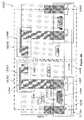
- FIG. 9Billustrates a layout of an embodiment of a 16 bit memory array that includes NMOS FET select transistors and CMOS buffer and control circuits.
- FIG. 10Ashows a top SEM image of an exemplary fabricated 16 bit memory array region that corresponds to the layout of FIG. 9B and shows nonvolatile nanotube storage nodes formed using nonvolatile nanotube block switches.
- FIG. 10Bshows a tilt angle SEM image of one of the exemplary nonvolatile nanotube block switches shown in of FIG. 10A .
- FIG. 11Ashows test results of write 0 and write 1 memory operations performed on the exemplary 16 bit memory array illustrated in FIGS. 9A-10B .
- FIG. 11Bshows a schmoo plot write 0 and write 1 operating voltages for individual bit (cell) locations in the exemplary 16 bit memory array illustrated in FIGS. 9A-10B .
- FIG. 11Cshows another schmoo plot of write 0 and write 1 operating voltages for individual bit (cell) locations in the exemplary 16 bit memory array illustrated in FIGS. 9A-10B .
- FIG. 12Aillustrates a top view of an embodiment of four memory array cells with nonvolatile nanotube switches used as nonvolatile nanotube storage nodes and formed on the top surface of the cell region.
- FIG. 12Billustrates a cross section of the memory array cell embodiment illustrated in FIG. 12A .
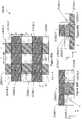
- FIG. 13Aillustrates a top view of an embodiment of four memory array cells with top/side and bottom contact terminal-type nonvolatile nanotube block switches used as nonvolatile nanotube storage nodes and formed on the top surface of the cell region.
- FIG. 13Billustrates a cross section of the memory array cell embodiment illustrated in FIG. 13A .
- FIG. 14Aillustrates a top view of an embodiment of four memory array cells with top and bottom contact terminal-type nonvolatile nanotube block switches used as nonvolatile nanotube storage nodes and formed on the top surface of the cell region.
- FIG. 14Billustrates a cross section of the memory array cell embodiment illustrated in FIG. 14A .
- FIG. 15illustrates a cross section of an embodiment of memory array cells with top and bottom contact terminal-type enclosed nonvolatile nanotube block switches used as nonvolatile nanotube storage nodes and formed on the top surface of the cell region.
- FIG. 16Aillustrates a top view of an embodiment of four memory array cells with nonvolatile nanotube switches used as nonvolatile nanotube storage nodes and integrated in the cell region in proximity to a corresponding select transistor and below the bit line.
- FIG. 16Billustrates a cross section of the memory array cell embodiment illustrated in FIG. 16A .
- FIG. 17Aillustrates a top view of an embodiment of four memory array cells with top/side and bottom contact terminal-type nonvolatile nanotube block switches used as nonvolatile nanotube storage nodes and integrated in the cell region in proximity to a corresponding select transistor and below the bit line.
- FIG. 17Billustrates a cross section of the memory array cell embodiment illustrated in FIG. 17A .
- FIG. 18Aillustrates a top view of an embodiment of four memory array cells with top and bottom contact terminal-type nonvolatile nanotube block switches used as nonvolatile nanotube storage nodes and integrated in the cell region in proximity to a corresponding select transistor and below the bit line;
- FIG. 18Billustrates a cross section of the memory array cell embodiment illustrated in FIG. 18A .
- FIG. 19illustrates a cross section of an embodiment of memory array cells with top and bottom contact terminal-type enclosed nonvolatile nanotube block switches used as nonvolatile nanotube storage nodes and integrated in the cell region in proximity to a corresponding select transistor and below the bit line.
- FIG. 20Aillustrates a cross section of an embodiment of memory array cells with top and bottom contact terminal-type nonvolatile nanotube block switches used as nonvolatile nanotube storage nodes and integrated in the cell region in proximity to a corresponding select transistor and positioned between a bit line contact and a drain of a corresponding select transistor.
- FIG. 20Bshows a comparison of estimated cell areas as a function of the type of nonvolatile nanotube storage node selected and the integration means used, according to some embodiments.
- FIG. 21illustrates a cross section of an embodiment of a cross point switch formed using a nonvolatile nanotube switch in an essentially horizontal orientation with a first center-region contact terminal and a second “picture frame” contact terminal surrounding the first contact.
- FIGS. 22A-22Cillustrate a plan view and two corresponding cross sections of embodiments of cross point switches formed using a first type of top and bottom contact terminal nonvolatile nanotube block switches.
- FIG. 22Dshows an embodiment nonvolatile electrically programmed wire routing connections corresponding to various ON and OFF combination of nonvolatile nanotube block switches illustrated in FIGS. 22A-22C .
- FIGS. 23A-23Cillustrate a plan view and two corresponding cross sections of embodiments of cross point switches formed using a second type of top and bottom contact terminal nonvolatile nanotube block switches.
- Some embodimentsprovide 2-D cell structures and enhanced 3-D cell structures that enable dense nonvolatile memory arrays that include two terminal nonvolatile nanotube storage nodes.
- the nodesinclude 2-D nanotube switches referred to as nonvolatile nanotube switches (NV NT switches) and/or 3-D nanotube switches referred to as nonvolatile nanotube block switches (NV NT block switches).
- the nodesalso include corresponding select transistors such as NMOS FETs (NFETs) that can write logic 1 and 0 states for multiple cycles, read stored logic states, and hold logic states without power applied to the memory node.
- NFETsNMOS FETs
- Some embodimentsare scalable to large memory array structures and/or are compatible with CMOS circuit manufacture.
- CMOS select deviceconsisting of both NFET and PFET devices may also be used instead of NMOS or PFET FET select transistors.
- NV NT block switchesmay be used as nonvolatile nanotube storage nodes in memory cells and as nonvolatile cross point switches in cross point switch matrix applications.
- NV NT block switchesmay be as small as F ⁇ F on each side, where F is a minimum technology node dimension, as described in greater detail in U.S. patent application Ser. Nos. 11/835,651, 11/835,759, 11/835,845, 11/835,852, 11/835,856, and 11/835,865, all filed Aug. 8, 2007, entitled “Nonvolatile Nanotube Diodes and Nonvolatile Nanotube Blocks and Systems Using Same and Methods of Making Same.”
- nanotube-based nonvolatile memory arraysmay also be configured as NAND and NOR arrays in PLA, FPGA, and PLD configurations, and that wire routing may also be configured using nanotube-based nonvolatile cross point switches in cross point switch matrices.
- Field programmable logicmay be reconfigured multiple-times using a combination of nanotube-based nonvolatile memory arrays and cross point switch matrices to form stand-alone and embedded logic functions as well.
- NV NT switchestwo-terminal 2-D nonvolatile nanotube switches
- NV NT block switchestwo terminal 3-D nonvolatile nanotube block switches
- FIG. 8Dwhich is described further below.
- NV NT switches or NV NT block switchesmay be formed at or near the top surface of memory arrays for ease of integration, or may be formed in cells close to select transistors for high density (small footprint) as described further below.
- memory cellsmay use nonvolatile nanotube storage nodes with NV NT switches or NV NT block switches formed (fabricated) at or near a top surface above substantially pre-wired memory cells in which select transistors (typically NFETs) are connected to array word lines (WLs) and bit lines (BLs).
- select transistorstypically NFETs
- WLsarray word lines
- BLsbit lines
- a studinterconnects the source of the NFET select transistor to a first terminal of a NV NT switch or NV NT block switch, while a second terminal is connected to a reference array line also referred to as a secondary word line (WWL).
- WWLsecondary word line
- NV NT switches or NV NT block switches at or near the top surface of memory arraysfacilitate nanotube switch integration because nearly all growth, deposition, and etch steps required by the semiconductor structure have been completed prior to nanotube deposition and patterning. Integrating nanotube switch structures near the end of the fabrication cycle enables rapid sample preparation since the memory arrays may be conventionally pre-formed to the stage where only nanotube switch formation is needed to complete fabrication.
- NV NT switches or NV NT block switches at or near the top surface of memory arraysmay be left unpassivated and may be hermetically sealed in a package, tested under typical conditions, and also evaluated for tolerance to harsh environments such as high temperatures and high radiation. Examples of unpassivated switches are illustrated in FIGS. 2A , 3 , and 4 A described further below.
- NV NT switches or NV NT block switches at or near the top surface of memory arraysmay be passivated and packaged using conventional packaging means. Such passivated packaged chips may be tested under typical conditions and also evaluated for tolerance to harsh environments such as high temperatures and high radiation. Examples of passivated switches are illustrated in FIGS. 5A , 6 A- 6 D, 7 A- 7 B, 8 A- 8 C as described further below.
- Passivated NV NT switches or NV NT block switchesmay also be integrated near an NFET select transistor, below the bit line, to achieve dense memory cells.
- NV NT block switches with top and bottom contactssuch as illustrated in FIG. 5A , may be integrated in memory cells that are, e.g., 6-8F 2 in density, where F is a minimum technology node.
- Memory cell size (footprint) estimates based on the nanotube switches summarized in FIG. 8Dare described in FIG. 20B , as described in greater detail below.
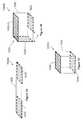
- FIGS. 1A-1Cillustrate perspective drawings of a thin nonvolatile nanotube element (NV NT element) and thicker nonvolatile nanotube elements referred to a nonvolatile nanotube blocks (NV NT blocks) with various contact locations.
- the combination of NV NT elements and contactsform two dimensional (2-D) NV NT switches and the combination of NV NT blocks and contacts form three dimensional (3-D) NV NT block switches as illustrated in FIGS. 1A-1C .
- 3-D NV NT block switchesmay be used instead of NV NT switches as nonvolatile nanotube storage nodes (NV NT storage nodes) in memory array cells as well as cross point switches for fabrication advantages and denser memory cell and cross point switch arrays as illustrated further below.
- NV NT switches and NV NT block switches illustrated in FIGS. 1A-1Care an exemplary subset of possible switch configurations, some embodiments of which are described in, e.g., U.S. patent application Ser. Nos. 11/835,651, 11/835,759, 11/835,845, 11/835,852, 11/835,856 an 11/835,865, entitled “Nonvolatile Nanotube Diodes and Nonvolatile Nanotube Blocks and Systems Using Same and Methods of Making Same,” all filed Aug. 8, 2007.
- NV NT switch 1000 A illustrated in perspective drawing in FIG. 1Ashows a NV NT switch with relatively thin (e.g., about 0.5 nm to less than 10 nm) nonvolatile nanotube element 1005 and bottom contact locations 1010 and 1015 .
- Contact locationsillustrate where terminals (not shown) contact the surface of nanotube element 1005 as described further below and in U.S. patent application Ser. No. 11/280,786.
- NV NT block switch 1000 B illustrated in perspective drawing in FIG. 1Bshows a NV NT block switch with NV NT block 1020 (e.g., typically 10 nm or greater in any given dimension) with a bottom contact location 1030 and a top/side contact location 1025 including top contact location 1025 - 2 and side contact location 1025 - 1 . Edges of bottom contact location 1030 and side contact location 1025 - 1 are separated by an overlap distance L OL . Contact locations illustrate where terminals (not shown) contact the surface of NV NT block 1020 as described further below and in U.S. patent application Ser. Nos.
- NV NT block switch 1000 C illustrated in perspective drawing in FIG. 1Cshows a NV NT block switch with NV NT block 1035 (e.g., 10 nm or greater in any given dimension) with a bottom contact location 1040 and a top contact location 1045 .
- Contact locationsillustrate where terminals (not shown) contact the surface of NV NT block 1035 as described further below and in U.S. patent application Ser. No. 11/835,651, 11/835,759, 11/835,845, 11/835,852, 11/835,856, and 11/835,865, all filed Aug.
- 3-D NV NT block switch 1000 Coccupies a relatively small area (has a relatively small footprint) relative to other embodiments of 3-D NV NT block switches and 2-D NV NT switches.
- NV NT switch 1000 Acorresponds to NV NT switch 2000 illustrated in FIG. 2A further below, where nanotube element 1005 A corresponds to nanotube element 2035 , contact location 1010 corresponds to the location of contact terminal 2010 , and contact location 1015 corresponds to the location of contact terminal 2015 .
- FIG. 2Aillustrated in more detail in U.S. patent application Ser. No. 11/280,786, illustrates NV NT Switch 2000 including patterned nanotube element 2035 on insulator 2030 , which is on the surface of combined insulator and wiring layer 2020 , which is supported by substrate 2025 .
- Patterned nanotube element 2035is a nanofabric on a planar surface, and partially overlaps and contacts terminals (conductive elements) 2010 and 2015 .
- Contact terminals 2010 and 2015are deposited and patterned directly onto combined insulator and wiring layer 2020 , which is on substrate 2025 , prior to patterned nanotube element 2035 formation.
- the nonvolatile nanotube switch channel length L SW-CHis the separation between contact terminals 2010 and 2015 .
- Substrate 2025may be an insulator such as ceramic or glass, a semiconductor, or an organic rigid or flexible substrate. Substrate 2025 may be also be organic, and may be flexible or stiff. Insulators 2020 and 2030 may be SiO 2 , SiN, Al 2 O 3 , or another insulator material.
- Terminals 2010 and 2015may be formed using a variety of contact and interconnect elemental metals such as Ru, Ti, Cr, Al, Al(Cu), Au, Pd, Ni, W, Cu, Mo, Ag, In, Ir, Pb, Sn, as well as metal alloys such as TiAu, TiCu, TiPd, PbIn, and TiW, other suitable conductors, or conductive nitrides, oxides, or silicides such as RuN, RuO, TiN, TaN, CoSi x and TiSi x .
- contact and interconnect elemental metalssuch as Ru, Ti, Cr, Al, Al(Cu), Au, Pd, Ni, W, Cu, Mo, Ag, In, Ir, Pb, Sn, as well as metal alloys such as TiAu, TiCu, TiPd, PbIn, and TiW, other suitable conductors, or conductive nitrides, oxides, or silicides such as RuN, RuO, TiN, TaN, CoS
- FIG. 2Billustrates an SEM image of a nonvolatile nanotube switch 2000 ′ prior to passivation and corresponds to nonvolatile nanotube switch 2000 in the cross sectional drawing in FIG. 2A .
- Nonvolatile nanotube switch 2000 ′includes nanofabric element 2035 ′, contact terminals 2010 ′ and 2015 ′ corresponding to contact terminals 2010 and 2015 , respectively, and an insulator 2020 ′ corresponding to insulator and wiring layer 2020 .
- Exemplary nonvolatile nanotube switchessuch as switch 2000 ′ have been fabricated with channel lengths L CHANNEL in the range of 250 nm to 22 nm thereby reducing nonvolatile nanotube switch size and lowering programming voltages, as described in more detail in U.S. patent application Ser. No. 11/280,786, although other suitable channel lengths can be used.
- Nonvolatile nanotube switchessuch as switch 2000 illustrated in a cross sectional drawing in FIG. 2A and corresponding to SEM micrograph of NV NT switch 2000 ′ illustrated in FIG. 2B has been cycled more than 50 million times between ON and OFF resistance states as illustrated by graph 2050 in FIG. 2C .
- the conducting (ON) state resistanceis typically in the range of 10 kOhms to 50 kOhms, while the nonconducting (OFF) state resistance typically exceeds 1 GOhm, for a greater than five orders of magnitude separation of resistance values between conducting and nonconducting ON and OFF switch states, respectively.
- FIG. 3illustrates NV NT Switch 3000 , a modification of NV NT switch 2000 illustrated in FIG. 2A , including patterned nanotube element 3045 supported by and in contact with contact terminals 3010 and 3015 , contact terminal extension 3040 in physical and electrical contact with terminal 3010 , and insulator 3035 .
- Insulator 3042completes the planarized structure but is typically not in contact with patterned nanotube element 3045 .
- NV NT switch 3000has approximately the same overall dimensions as NV NT switch 2000 , except that insulators 3030 and 3035 and extended contact terminal 3040 have been added to the basic NV NT switch 2000 structure using known preferred methods of fabrication to reduce NV NT switch 3000 channel length to shorter L SW-CH as illustrated in FIG. 3 .
- Shorter L SW-CH channel lengthmay reduce NV NT switch 3000 operating voltage, as described in U.S. patent application Ser. No. 11/280,786, because L SW-CH length may be in the 5 to 50 nm length range, for example, while contact terminals 3010 and 3015 may be separated by 150 to 250 nm, for example.
- L SW-CH lengthis determined in part by the thickness of insulator 3035 as deposited on exposed upper regions of contact terminals 3010 and 3015 using known preferred sidewall spacer methods, such as those described in prior art U.S. Pat. No. 4,256,514 the entire contents of which are incorporated herein by reference.
- Exposed upper regions of contact terminals 3010 and 3015may be in the range of 10 to 500 nm, for example.
- the top surface 3030 ′ of insulator 3030may be formed by preferred industry methods of selective directional etch of insulator 3030 to a desired depth below the top surface of coplanar contact terminals 3010 and 3015 .
- Insulator 3030 and contact terminals 3010 and 3030are in contact with insulator and wiring layer 3020 , which is on substrate 3025 .
- Insulator 3035is deposited using known preferred industry methods to a thickness corresponding to a desired switch channel length L SW-CH such as 5 to 50 nm, for example, and then patterned using preferred methods.
- insulator 3042is formed using preferred methods of deposition and planarization. Then, preferred methods pattern nanotube element 3045 as described in incorporated patent applications.
- Substrate 3025may be an insulator such as ceramic or glass, a semiconductor, or an organic rigid or flexible substrate. Substrate 3025 may be also be organic, and may be flexible or stiff. Insulators 3020 , 3030 , 3035 , and 3042 may be SiO 2 , SiN, Al 2 O 3 , or another insulator material.
- Contact terminals 3010 and 3015 and contact terminal extension 3040may be formed using a variety of contact and interconnect elemental metals such as Ru, Ti, Cr, Al, Al(Cu), Au, Pd, Ni, W, Cu, Mo, Ag, In, Ir, Pb, Sn, as well as metal alloys such as TiAu, TiCu, TiPd, PbIn, and TiW, other suitable conductors, or conductive nitrides, oxides, or silicides such as RuN, RuO, TiN, TaN, CoSi x and TiSi x .
- contact and interconnect elemental metalssuch as Ru, Ti, Cr, Al, Al(Cu), Au, Pd, Ni, W, Cu, Mo, Ag, In, Ir, Pb, Sn, as well as metal alloys such as TiAu, TiCu, TiPd, PbIn, and TiW, other suitable conductors, or conductive nitrides, oxides, or silicides such as RuN, RuO
- NV NT switches 2000 and 3000are illustrated without an overlying insulating protective layer. If NV NT switches are formed on the top layer of a semiconductor chip, then no insulation is required for chip operation. However, chips typically are mounted in hermetically sealed packages to ensure protection from mechanical handling and environmental contamination and moisture. If NV NT switches are to be integrated closer to the semiconductor substrate, or not hermetically sealed, then NV NT switches may be protected using insulating layers as described further below with respect to FIGS. 5A , 6 A- 6 D, 7 A, 7 B, and 8 A- 8 C.
- FIG. 4Adescribed in more detail in U.S. Provisional Patent Application No.
- Switch 4000occupies approximately the same area as NV NT switches 2000 and 3000 .
- NV NT block switch 4000also features NV NT block overlap length L OL which is determined by the separation between bottom contact terminal 4015 and an edge of NV NT block 4035 .
- NV NT block switch 4000includes a combination of side/top contact 4040 formed by side surface contact 4040 A and top surface contact 4040 B and bottom surface contact 4042 formed by contact terminal 4015 .
- Bottom surface contact 4042corresponds to bottom surface contact location 1030 in NV NT block switch 1000 B illustrated in perspective drawing in FIG.
- top/side surface contact 4040corresponds to top/side surface contact location 1025
- top surface contact 4040 Bcorresponds to top surface contact location 1025 - 2
- side surface contact 4040 Acorresponds to side surface location 1025 - 1
- NV NT block 4035corresponds to NV NT block 1020 .
- An effective overlap length L OLis the distance between the edges of bottom surface contact 4042 and side/top surface contact 4040 described further below.
- Contact terminal 4010is connected to side/top surface contact 4040 by conductor 4045 . Preferred methods of fabrication may be used to simultaneously deposit and pattern conductor 4045 and surface contact 4040 , thereby forming combined conductor/contact 4045 / 4040 interconnect means.
- NV NT block side surfacesmay be partially defined by preferred methods of directional etching the exposed portions of the nanotube block fabric using combined conductor/contact 4045 / 4040 as a mask.
- NV NT block 4035 side surface 4043(and two other sides not visible in FIG. 4A ) are exposed. Methods of etching nanotube fabric layers are described in the incorporated patent references.
- Contact terminals 4010 and 4015are deposited and patterned directly onto combined insulator and wiring layer 2020 , which is on substrate 4025 , prior to patterned nanotube block 4035 formation.
- Substrate 4025may be an insulator such as ceramic or glass, a semiconductor, or an organic rigid or flexible substrate.
- Substrate 4025may be also be organic, and may be flexible or stiff.
- Insulators 2020 and 4030may be SiO 2 , SiN, Al 2 O 3 , or another insulator material.
- Terminals 4010 and 4015may be formed using a variety of contact and interconnect elemental metals such as Ru, Ti, Cr, Al, Al(Cu), Au, Pd, Ni, W, Cu, Mo, Ag, In, Ir, Pb, Sn, as well as metal alloys such as TiAu, TiCu, TiPd, PbIn, and TiW, other suitable conductors, or conductive nitrides, oxides, or silicides such as RuN, RuO, TiN, TaN, CoSi x and TiSi x .
- contact and interconnect elemental metalssuch as Ru, Ti, Cr, Al, Al(Cu), Au, Pd, Ni, W, Cu, Mo, Ag, In, Ir, Pb, Sn, as well as metal alloys such as TiAu, TiCu, TiPd, PbIn, and TiW, other suitable conductors, or conductive nitrides, oxides, or silicides such as RuN, RuO, TiN, TaN,
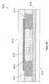
- FIG. 5Aillustrates two identical memory cells, cell 1 and cell 2 , of a 3-D diode-steering memory array described further in U.S. patent application Ser. Nos. 11/835,651, 11/835,759, 11/835,845, 11/835,852, 11/835,856, and 11/835,865, all filed Aug. 8, 2007, entitled “Nonvolatile Nanotube Diodes and Nonvolatile Nanotube Blocks and Systems Using Same and Methods of Making Same.”
- Cell 1(identical to cell 2 ) includes steering diode 5010 with one terminal in contact with NV NT block switch 5005 at bottom surface contact terminal 5020 , and another diode 5010 terminal in contact with array wiring conductor 5015 .
- NV NT block switch 5005top contact 5040 is in contact with array wiring conductor 5050 .
- NV NT block switch 5005includes top contact 5040 in contact with NV NT block 5030 and bottom contact 5020 in contact with NV NT block 5030 .
- NV NT block switch 5005is embedded in dielectric 5060 .
- NV NT block switch 5005is relatively dense (occupies a relatively small footprint) because top and bottom contacts and NV NT block 5030 side surfaces can be defined by self-aligned trench preferred methods of fabrication described further in the incorporated patent references and may be used to form minimum NV NT storage node dimensions of F ⁇ F.
- NV NT block switch 5005is illustrated as integrated with diode 5010 select (steering) devices, NV NT block switch 5005 may be combined with NFET select devices to form relatively dense memory arrays as described further below with respect to FIGS. 18A-18C for example.
- FIG. 1Cillustrates NV NT block 1035 corresponding to NV NT block 5030 illustrated in FIG. 5A .
- Bottom contact location 1040corresponds to bottom contact 5020 and top contact location 1045 corresponds to top contact 5040 .
- NV NT block switch 5010may be as small as minimum dimensions F ⁇ F.
- NV NT block 5030 lateral dimensionsmay be larger than the minimum dimension F; the NV NT block 5030 side dimensions need not be equal.
- the vertical (thickness) dimension of NV NT block switch 5010is generally unconstrained by the minimum dimension F provided by the technology node. Instead, the vertical (thickness) dimension is related to the thickness of the nanotube fabric, which can be selected, e.g., to be sufficiently thick to substantially inhibit electrical contact between contacts 5020 and 5040 , as described in greater detail in U.S. patent application Ser. Nos.
- contact and conductors materialsinclude elemental metals such as Al, Au, W, Ta, Cu, Mo, Pd, Ni, Ru, Ti, Cr, Ag, In, Ir, Pb, Sn, as well as metal alloys such as TiAu, TiCu, TiPd, PbIn, and TiW, other suitable conductors, or conductive nitrides such as TiN, oxides, or silicides such as RuN, RuO, TiN, TaN, CoSi x and TiSi x .
- Insulatorsmay be SiO 2 , SiN, Al 2 O 3 , or another insulator material.
- NV NT switchesFor chips with NV NT switches that are packaged in non-hermetically sealed environments, then one or several insulator layers may be added to the NV NT switch structure. Also, for denser memory cells for example, NV NT switches may be integrated near a cell select transistor such as NFET, close to a silicon substrate and below bit line arrays wires for example. Therefore, multiple insulating layers may be used above NV NT switches integrated in some memory array structures. Insulators may interact with nanotube elements to change electrical properties of NV NT switches such as voltage threshold and current values required for switching. Some insulators may enhance electrical characteristics by lowering threshold voltages and currents. Examples of NV NT switch insulator approaches are illustrated further below with respect to FIGS. 5A , 6 A- 6 D, 7 A, 7 B, and 8 A- 8 C. In some cases, adding one or more insulating layers may involve the use of one or more additional masking layers.
- NV NT block switchesmay be fabricated with a top contact to a conductor such that insulators are not in contact with the top surface of NV NT block structures as illustrated in FIGS. 1B and 1C , and FIGS. 4A and 5A . However, insulators may be in contact with some sidewall surfaces for NV NT block switch structures illustrated in FIGS. 4A and 5A .
- NV NT block switchesoperate with a wide variety of contact configurations such as top and bottom and top/side and bottom contacts as illustrated in FIGS. 4A-4B and 5 A- 5 B, as well as and other contact configurations such as end-only, end and side-contacts, and other contact options illustrated further in the incorporated patent references.
- NV NT block switchesmay have contacts to conductors-only (no insulators) on five of six faces, leaving only a small portion of a bottom NV NT block region in contact with an underlying insulator by forming covered or enclosed (enrobed) NV NT block switches as illustrated further below with respect to FIG. 8C .
- Such covered or enclosed NV NT block switchesmay integrate more easily at various levels of assembly than NV NT switches and other (non-enclosed) NV NT block switches because of reduced sensitivity of nanotube electrical characteristics to various insulators commonly used in integrated circuit processes and structures.
- covered or enclosed NV NT block switchesmay be compatible with a broader range of insulators used in integrated circuit manufacturing.
- covered or enclosed NV NT block switchesmay be less dense (have a larger footprint) than NV NT block switch 5000 with top and bottom contacts as illustrated in FIG. 5A .
- Passivation layersmay have some or all of the following properties.
- the passivation layermay form an effective moisture barrier, substantially preventing exposure of the nanotubes to water.
- the passivation filmmay not interfere with, and, preferably, enhance the switching mechanism of the memory device.
- the passivation filmmay be compatible with other insulators, conductors, and semiconductors with respect to the preferred process flow used to form the integrated structure.
- Passivation layersmay be formed from any appropriate material known in the CMOS industry, including, but not limited to: SiO 2 , SiN, Al 2 O 3 , polyimide, and other insulating materials such as PSG (Phosphosilicate glass) oxide, LTO (planarizing low temperature oxide) oxide, sputtered oxide or nitride, flowfill oxide, CVD (chemical vapor deposition) of oxide and nitride, ALD (atomic layer deposition) oxides. PVDF (Polyvinylidene Fluoride) insulating material may also be used. Combinations of these insulators, or other suitable insulators, may also be used.
- Insulators 6010 and 2030may also be formed using preferred methods to deposit and pattern sacrificial polymer polypropylene carbonate (PPC) dissolved in one or more organic solvents such as NMP or cyclohexanone available in the industry.
- PPCpolypropylene carbonate
- a description of the properties of polypropylene carbonatemay be found, for example, in referenced technical data available from the company Empower Materials, Inc.
- Other sacrificial polymerssuch as UnityTMsacrificial polymer and polyethylene carbonate sacrificial polymer may also be used. Information about UnityTM polymer is available from the supplier BFGoodrich, Cleveland, Ohio. Sacrificial polymer usage is further described in the incorporated patent references. These materials may also be used in conjunction with other materials, i.e., PPC or UnityTM polymers with insulators such as SiO 2 as illustrated further in the incorporated patent references.
- FIG. 6Billustrates insulated NV NT switch 6020 formed by adding insulator 6025 in contact with patterned nanotube element 2035 and insulator 6030 in contact with insulator 6025 , contact terminals 2010 and 2015 , and portions of insulator 2030 to NV NT switch 2000 illustrated in FIG. 2A .
- Insulator 6025may be formed by preferred methods of applying sacrificial polymers such as PPC and Unity described further above.
- Insulator 6030may be formed by preferred methods of applying an insulator such as SiO 2 for example.
- FIG. 6Dillustrates insulated NV NT switch 6060 which corresponds to NV NT switch 6040 .
- sacrificial insulators(not shown) have been evaporated through insulator 6050 to create gap region 6065 above patterned nanotube element 2035 and gap region 6065 ′ below nanotube element 2035 , embedded in insulator 6070 below patterned nanotube element 2035 .
- Enhanced performance characteristics of NV NT switches having patterned nanotube elements with gap regionsare described further in the incorporated patent references.
- FIG. 7Aillustrates insulated NV NT Switch 7000 with self aligned channel length L SW-CH formed by adding insulator 7010 to NV NT switch 3000 illustrated in FIG. 3 .
- Patterned nanotube element 3045contacts underlying contact terminals 3010 and 3015 , contact terminal extension 3040 , and insulator 3035 .
- Patterned nanotube element 3045also contacts overlying insulator 7010 . Passivation layers are described further above and also further below and in the incorporated patent references.
- FIG. 8Aillustrates an insulated NV NT block switch 8000 which is similar to non-insulated NV NT block switch 4000 illustrated further above in FIG. 4A .
- Insulated NV NT block switch 8000may be used instead of NV NT switches illustrated in FIGS. 6A-6D and 7 A and 7 B in memory cells.
- NV NT block switch 8000 illustrated in FIG. 8Ais formed by depositing insulator 8010 on the surface of NV NT block switch 4000 such that insulator 8010 is in contact with conductor 4045 , including the contact 4040 region, exposed side surfaces such as side surface 4043 of NV NT block 4035 , and insulator 4030 .
- Insulator 8010is not in contact with the top surface of NV NT block 4035 because contact 4040 B is covered by conductor 4045 , and is also not in contact with one side surface of NV NT block 4035 because contact 4040 A is covered by conductor 4045 .
- Insulator 8010 materialmay be similar to insulator 6010 material described further above with respect to FIG. 6A .
- NV NT block switch 8020 illustrated in FIG. 8Bis formed by including sacrificial polymer regions (not shown) similar to sacrificial regions described further above with respect to FIGS. 6A-6D and 7 A- 7 B prior to forming insulator 8030 .
- Such sacrificial polymer regionsmay remain in the insulator structure as illustrated in FIG. 6B further above, or may be evaporated through an insulator such as insulator 8030 to form gap regions such as illustrated in FIGS. 6C and 6D .
- Gap region 8040prevents contact between insulator 8030 and exposed side surface 4043 of NV NT block 4035 .
- Other NV NT block 4035 side surfaces(not visible in FIG.
- NV NT block 4035may include gap regions that prevent side surface contact between NV NT block 4035 and insulator 8030 . Gap regions and preferred methods of fabrication are described further above with respect to FIGS. 6C , 6 D, and 7 B, and in the incorporated patent references.
- NV NT block switcheshave been demonstrated to electrically operate (switch between ON and OFF states) in a wide variety of geometries and contact configurations such as top and bottom and top/side and bottom contacts as illustrated in FIGS. 4A and 5A , as well as other contact configurations such as end-only, end and side-contacts, and other contact options, such as those illustrated in U.S. patent application Ser. Nos. 11/835,651, 11/835,759, 11/835,845, 11/835,852, 11/835,856, and 11/835,865, all filed Aug.
- Nonvolatile Nanotube Diodes and Nonvolatile Nanotube Blocks and Systems Using Same and Methods of Making SameFor flexibility and ease of integrating NV NT block switch-type configurations at nearly any level of semiconductor (or other type of) process flow with exposure to various materials and processes, it may be desirable to integrate NV NT block switches in such a way as to enhance conductor contacts and to reduce non-conductor (insulator) contacts to side/top/bottom surfaces (faces) of NV NT blocks regions.
- a covered or enclosed (e.g., enclosed by conductor contacts) NV NT block configurationenables covered or enclosed NV NT block switches with contacts to conductors-only (no insulators) on five of six NV NT block surfaces (faces), leaving only a small portion of a bottom NV NT block surface in contact with an underlying insulator as described further below with respect to FIG. 8C and referred to as overlap length L OL .
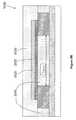
- FIG. 8Cillustrates enclosed (enrobed) NV NT block switch 8050 cross section, which includes bottom contact terminal 8065 in contact with insulator and wiring layer 8055 , which in turn is in contact with substrate 8060 .
- the top surface of bottom contact terminal 8065 and insulator 8070are coplanar.
- Bottom contact terminal 8065contacts NV NT block 8075 at bottom contact 8067 .
- NV NT block 8075extends beyond the surface of bottom contact 8067 by an overlap distance L OL on all sides and is in contact with the top surface of insulator 8070 .
- L OLmay be on the order of 5 to 100 nm, for example.
- L OLmay be determined by mask alignment or by self aligned techniques using known preferred sidewall spacer methods as described in prior art U.S. Pat. No. 4,256,514 combined with preferred methods such as chemical-mechanical polishing (CMP) techniques as described in prior art U.S. Pat. No. 4,944,836, as illustrated further above with respect to FIG. 3
- a conductorencloses NV NT block 8075 on the top surface and on all side surfaces thereby forming a top/side contact terminal 8080 .
- Top portion 8080 A of top/side contact terminal 8080forms top contact 8083 with the top surface of NV NT block 8075 .
- Preferred methods of fabricationmay use top portion 8080 A of top/side contact terminal 8080 as a masking layer when forming the sidewall surfaces of NV NT block 8075 .
- Sidewall conductor regions 8080 B- 1 , 8080 B- 2 of top/side contact terminal 8080 , and other sidewall regions not visible in FIG. 8Cmay be formed by preferred methods to deposit a conformal conductor layer and then directionally etching as shown in prior art U.S. Pat. No.
- sidewall conductor regions 8080 B- 1 and 8080 B- 24,256,514 to form sidewall conductor regions 8080 B- 1 and 8080 B- 2 .
- Preferred directional etch methodsremove the remaining portions of conductor material on the surface of insulator 8070 .
- Sidewall conductor regions 8080 B- 1 and 8080 B- 2form sidewall contacts 8082 - 1 and 8082 - 2 to side surfaces of NV NT block 8075 .
- Preferred methodsdeposit insulator 8085 .
- preferred methodsetch via hole 8087 to the top portion 8080 A of top/side contact terminal 8080 .
- preferred methodsdeposit a conductor layer that fills via hole 8087 .
- preferred methodssuch as CMP described in the incorporated patent references planarize the surface forming conductor 8090 in contact with the top surface 8080 A of top/side contact terminal 8080 .
- enclosed NV NT block switch 8050 dimensionsmay be larger than the minimum dimension F by two-times the amount of the overlap length L OL (2 L OL ) and two-times the thickness of sidewall conductors regions 8080 B- 1 and 8080 B- 2 .
- L OLis 5 to 50 nm
- the sidewall conductor regions 8080 B- 1 and 8080 B- 2are 5 to 50 nm
- the minimum dimensions of enclosed NV NT block switch 8050 dimensionsare F+20 nm in cross section to F+200 nm in cross section.
- contact and conductors materialsinclude elemental metals such as Al, Au, W, Ta, Cu, Mo, Pd, Ni, Ru, Ti, Cr, Ag, In, Ir, Pb, Sn, as well as metal alloys such as TiAu, TiCu, TiPd, PbIn, and TiW, other suitable conductors, or conductive nitrides such as TiN, oxides, or silicides such as RuN, RuO, TiN, TaN, CoSi x and TiSi x .
- Insulatorsmay be SiO 2 , SiN, Al 2 O 3 , or another insulator material.
- Enclosed NV NT block switch 8050may be combined with a select transistor such as an NFET to create memory cells as illustrated further below with respect to FIG. 19 for example.
- NV NT switches and NV NT block switchesmay be integrated with NFET select transistors to form nonvolatile memory cells and arrays of same.
- Such nanotube switchesmay be placed at or near a top surface region above already partially formed cells that include NFET select devices connected to word lines (WLs) and bit lines (BLs) for ease of integration.
- FIGS. 16A , 16 B, 17 A, 17 B, 18 A, 18 B, and 19Various memory array cells using NV NT switches and NV NT block switches described further above and summarized in FIG. 8D are described further below with respect to FIGS. 16A , 16 B, 17 A, 17 B, 18 A, 18 B, and 19 .
- These memory cellsuse NV NT storage nodes formed of NV NT switches and NV NT block switches integrated within cells in close proximity to NFET select devices, with one terminal connected to the source of the NFET transistor, and below the bit line layer to enhance cell density.
- FIG. 20Billustrates the cell areas (footprints) of various NV NT storage nodes formed with NV NT switches or NV NT block switches.
- Cell areasare expressed in terms of the number of minimum squares of dimension F ⁇ F.
- NV NT storage nodes located at or near a surface above pre-wired cell regionscell areas depend on whether self-aligned or non-self aligned studs are used to contact the source of the NFET select transistor with one terminal of the NV NT switch or NV NT block switch.
- NV NT block switches with top and bottom contactsreferred to as node # 10
- Nonvolatile memory array schematic 9000includes a matrix of 16 nonvolatile storage cells C 00 , C 10 , . . . , C 33 as illustrated in FIG. 9A .
- Memory arraysare not limited to 16 cells and may have millions or billions of cells for example.
- Each memory cell illustrated in memory array schematic 9000such as representative cell C 00 , includes a select transistor T 00 that may be an NFET as shown, or may also be a PFET (not shown) or a CMOS transfer device (not shown) that includes both NFET and PFET devices, or other types of switching devices (not shown).
- Each cell, such as cell C 00also includes a nonvolatile nanotube storage node NT 00 .
- Nonvolatile nanotube storage node NT 00(NV NT storage node) may be formed using NV NT switch-types and NV NT block switch-types such as those illustrated further above and summarized in FIG. 8D .
- Nonvolatile storage cellssuch as cell C 00 are formed by connecting the source SC 00 of a transistor such as NFET T 00 to a first terminal of a NV NT storage node such as NV NT storage node NT 00 illustrated in FIG. 9A . Examples of NV NT storage nodes are listed in FIG. 8D .
- Memory array schematic 9000is formed by connecting word lines WL 0 , WL 1 , WL 2 , and WL 3 to corresponding gates of NFET select transistors in corresponding storage cells; connecting secondary word lines WWL 0 , WWL 1 , WWL 2 , and WWL 3 to corresponding second terminals of NV NT storage nodes in corresponding storage cells; and connecting bit lines BL 0 , BL 1 , BL 2 , and BL 3 to corresponding drain diffusions of corresponding NFET select transistors in corresponding nonvolatile storage cells as illustrated in FIGS. 9A and 9B .
- word line WL 0is connected to the gate of NFET T 00 by contact GC 00 ; secondary word line WWL 0 is connected to the second terminal of nonvolatile nanotube storage node NT 00 by contact NC 00 ; and bit line BL 0 is connected to the drain of T 00 by contact DC 00 .
- Memory array layout 9002 illustrated in planar view in FIG. 9Bis a layout (design) of an exemplary 16 bit memory array corresponding to memory array schematic 9000 using 250 nm CMOS design rules. Selected design workstation layout levels are highlighted.
- Cells C 00 and C 10 of memory array layout 9002 illustrated in FIG. 9Bare formed within the same FET region 9005 and share a common drain diffusion.
- Word line WL 0contacts the gate of the cell C 00 select NFET transistor at contact 9007 , which corresponds to contact GC 00 between word line WL 0 and the gate of NFET T 00 in memory array schematic 9000 illustrated in FIG. 9A .
- Drain contact 9010is shared by mirror-image cells C 00 and C 10 C illustrated in FIG. 9B , and contacts conductor segment 9015 which in turn contacts bit line BL 0 through contact 9020 .
- Contact 9010 illustrated in FIG. 9Bcorresponds to drain contacts DC 00 of NFET T 00 and DC 10 of NFET T 01 illustrated in FIG.
- a first contact to nonvolatile nanotube storage node NT 00 illustrated in FIG. 9Ais connected to the source of NFET T 00 by contact SC 00 .
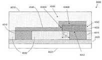
- NV NT block switch 4000 illustrated in FIG. 4A(NV NT storage node number 9 in FIG. 8D ) is placed above the source of the cell C 00 select NFET with NV NT block 4035 bottom contact 4015 extended to contact the cell C 00 NFET source diffusion as illustrated further below with respect to FIG. 13B .
- Combined upper/side contact 4040 to NV NT block 4035is connected to (part of) conductor 4045 illustrated in FIG. 4A and corresponds to conductor segment 9030 in FIG. 9B .
- Conductor segment 9030is also connected to second word line WWL 0 by contact 9035 , which corresponds to contact NC 00 in FIG. 9A .
- All C 10 NFET select devices and NV NT block switchesare interconnected in a corresponding manner to those described with respect to cell C 00 . All other cells correspond to cell C 00 or a mirror image of cell C 00 as described further above.
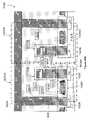
- SEM image 10000 illustrated in FIG. 10Ashows a plan view of partially fabricated memory cells just prior to the formation of NV NT block switches corresponding to NV NT block switch 4000 illustrated in FIG. 4A , which are formed above underlying cell select transistors and array wiring corresponding to memory array layout 9200 .
- a blanket (porous) nanotube fabric layer of approximately 40 nm thick deposited using preferred methodscovers the surface insulator and wiring layer 10200 but is not visible in this SEM image due to insufficient contrast.
- a corresponding (porous) patterned nanotube blockis illustrated further below by an SEM image in FIG. 10B .
- the blanket nanotube fabric layerwas deposited using spray coating.
- a blanket nanotube fabric layermay also be formed by spin coating multiple individual nanotube fabric layers.
- Contact terminal 10100 illustrated in FIG. 10Acorresponds to contact terminal 4010 illustrated in FIG. 4A and contact terminal 10150 corresponds to contact terminal 4015 .
- the blanket nanotube fabric layer not visible in SEM image 10000is in contact with the top coplanar surfaces of contact terminals 10100 and 10150 and with the top surface of insulator and wiring layer 10200 , which corresponds to insulator and wiring layer 4030 in FIG. 4A .
- Patterned mask 10250 images on the surface of the blanket nanotube fabric layer and overlapping contact terminals 10150are used to protect the underlying portion of the blanket nanotube fabric layer from an oxygen plasma etch step later in the process flow.
- Patterned mask images 10250may be formed using Al 2 O 3 , or Ge, or any other compatible hard mask material.
- preferred methodsetch the exposed portion of the blanket nanotube fabric layer in an oxygen plasma for example, as described further in the incorporated patent references.
- preferred methodsremove patterned mask 10250 images.
- preferred methodsform conductor segments 10400 shown in SEM image 10300 illustrated in FIG. 10A corresponding to conductor segment 9030 illustrated in FIG. 9B and conductor 4045 illustrated in FIG. 4A .
- Conductor segment 10400also forms a top/side contact to the underlying NV NT block (not visible) corresponding to contact 4040 illustrated in FIG. 4A .
- conductor segment 10400is formed of Ti/Pd of thickness 2/100 nm, although other metals may be used.
- NV NT block switches 10450corresponding to NV NT block switch 4000 illustrated in FIG. 4A with conductor segment 10400 corresponding to combined top/side contact 4040 and conductor 4045 , and bottom contact 10150 corresponding to bottom contact 4042 , respectively.
- SEM image 10300 of FIG. 10Ashows a plan view of top layers.
- the NV NT block corresponding to NV NT block 4035 in FIG. 4Ais not visible in SEM image 10300 .
- Insulator and wiring layer 10200 ′corresponds to insulator and wiring layer 10200 but without the blanket nanotube fabric layer.
- SEM image 10500 illustrated in FIG. 10Billustrates an SEM tilt cross section image.
- Contact terminal 10550 on the surface of insulator and wiring layer 10600corresponds to contact terminal 10150 in SEM image 10300 and forms a bottom contact to NV NT block 10650 .
- Top contact terminal 10700corresponds to that region of conductor segment 10400 in SEM image 10300 that forms a top contact to NV NT block 10650 .
- NV NT block 10650is approximately 25 ⁇ 80 nm in this example.
- Test and characterization of the 16 bit memory array 9000 illustrated in schematically in FIG. 9A , in layout form with NV NT block switch storage devices illustrated in FIG. 9B , and in an SEM image 10300 of the NV NT block switch storage region formed on top layers of the 16 bit memory array structure as illustrated in FIG. 10Ais carried out based on ON/OFF state switching and resistance state readout.
- ON/OFF state switching results for NV NT block switchesare illustrated by waveforms 4500 in FIG. 4B for switching using a single pulse of approximately 6 volts for transition between ON and OFF states.
- FIG. 9AON/OFF state switching results for NV NT block switches are illustrated by waveforms 4500 in FIG. 4B for switching using a single pulse of approximately 6 volts for transition between ON and OFF states.
- ON resistance valuesare typically in the 100's of KOhm range, and OFF resistance values are typically in the giga-Ohm range. If multiple pulses are used for write 0 and write 1 operation, switching voltages may be lower than 6 volts for example.
- Write 0 , write 1 , and read voltage and current waveformsmay be as described in U.S. patent application Ser. No. 11/280,786 and U.S. patent application Ser. Nos 11/835,651, 11/835,759, 11/835,845, 11/835,852, 11/835,856 and 11/835,865, entitled “Nonvolatile Nanotube Diodes and Nonvolatile Nanotube Blocks and Systems Using Same and Methods of Making Same,” all filed Aug. 8, 2007.
- write 0 , write 1 , and read operationsmay be performed by word and bit lines with secondary word lines at a reference voltage such as ground.
- write 0 and write 1 pulsesmay be applied using secondary word lines with cells selected by a corresponding word line, thereby reducing the voltage across cell select transistors and CMOS buffer circuits.
- This ability to change applied voltage polarity and current directionis enabled by the bidirectional properties of NV NT block switches (also applies to NV NT switches) that switch regardless of the applied voltage polarity and current flow direction.
- Display readout 11000 illustrated in FIG. 11Ashows the results of write 0 , write 1 , and read operations on an exemplary 16 bit memory array 9000 with NV NT block switches as described further above.
- a write 0 operationall four bits along a selected word line are erased simultaneously.
- bit lines BL 0 , BL 1 , BL 2 , and BL 3are all held at zero volts and a selected word line such as word line WL 0 is switched from 0 volts to a higher voltage such as 5 volts for example.
- one or several voltage pulse/pulsesis/are applied to corresponding secondary word line WWL 0 .
- the WWL 0 pulse amplitudemay be varied from 4 to 8 volts, for example.
- Corresponding NV NT block switch NT 00switches from ON to OFF, or remains in the OFF state.
- Write 0 operationsare repeated with WL 1 and WWL 1 , WL 2 and WWL 2 , and WL 3 and WWL 3 until all bits are in on OFF state.
- Bit pattern 11100 illustrated in FIG. 11Arepresents a write 0 (OFF state) for each of the 16 bits in 16 bit memory array 9000 such that each bit is an OFF or high resistance state.
- bit line BL 0For a read operation, a bit line such as bit line BL 0 is switched to a voltage less than 3 or 4 volts, for example, and a selected word line such as word line WL 0 activates an NFET select transistor such as T 00 to an ON state and connects BL 0 through a corresponding NV NT block such as NT 00 to corresponding secondary word line such as WWL 0 which is grounded. If the corresponding NV NT block switch NT 00 is in an OFF state, BL 0 remains unchanged and a “0” or OFF state is detected.
- bit line BL 0 voltageis reduced (droops) and a “1” state is detected.
- a read operationresults in bit pattern 11150 where all bits are in a “0” or OFF state such that output bit pattern 11150 corresponds to input bit pattern 11100 .
- a write 1 operationis performed one bit at a time along a selected word line such as WL 0 and corresponding secondary word line WWL 0 , for example.
- a logic “1” or low resistance stateis written in cell C 00 by holding bit line BL 0 at zero volts, while bit lines BL 1 , BL 2 , and BL 3 are held at a higher voltage such as 4 or 5 volts for example. Then, one or several voltage pulse/pulses is/are applied to corresponding secondary word line WWL 0 .
- the WWL 0 pulse amplitudemay be varied from 4 to 8 volts, for example, and cell C 00 switches from a logic “0” high resistance state and stores a nonvolatile logic “1” or low resistance state on NT 00 .
- C 01is to store a zero in this example, therefore no pulses are applied since the entire array was erased prior to the write 0 operation as described further above with respect to write 0 operations.
- the write 1 operationproceeds one bit at a time as described above with respect to the write 1 operation description further above until checkerboard pattern 11200 is written in memory array 9000 .
- checkerboard pattern 11200is applied to the pre-erased 16 bit memory array 9000 .
- a read operationresults in a corresponding checkerboard bit pattern 11250 , and the 16 bits in memory array 9000 remain stored in nonvolatile logic “0” or “1” state as illustrated by display readout 11000 .
- Individual NV NT block switches 10450 illustrated in FIG. 10Aare switched between ON and OFF, low and high resistance states respectively, as a function of applied voltages as described further above.
- fast rise and fall timessuch as 2 ns are used.
- slow rise and fall timessuch as 10 us are used.
- 10 pulseswere used for both write 0 and write 1 switching.
- hold time of 20 us for write 0 and 1 ms for write 1are used.
- test conditionsare similar to those described with respect to ON/OFF switching described with respect to FIGS. 4B and 5B and U.S. patent application Ser. No.
- Schmoo plot 11400 illustrated in FIG. 11Bshows pass and fail regions for write 0 operations in a range of 1 to 7 volts along the horizontal axis and write 1 operations in a range of 1 to 7 volts in the vertical direction.
- Pass region 11450shows that write 0 and write 1 operations with applied voltages of 4 volts and above result in successful switching of NV NT block switches similar to NV NT block switches 10450 .
- Write 0 and write 1 voltages outside pass region 11450are fails.
- Schmoo plot 11500 illustrated in FIG. 11Cshows pass and fail regions for write 0 operations in a range of 1 to 12 volts along the horizontal axis and write 1 operations in a range of 1 to 12 volts in the vertical direction.
- Pass region 11550shows that write 0 and write 1 operations with applied voltages of 4 volts and above result in successful switching of NV NT block switches similar to NV NT block switches 10450 .
- Write 0 and write 1 voltages outside pass region 11550are fails.
- One exceptionis a NV NT block switch that, in some embodiments, switches at a minimum of 5 volts for the write 1 operation as indicated by location 11600 .
- Memory arraysmay be formed by interconnecting nonvolatile memory cells that include a select transistor such as an NFET, a nonvolatile nanotube storage node such as a NV NT switch or a NV NT block switch, and interconnects within the cell and between the cell and array lines such as word lines, bit lines, and secondary word lines as shown in memory array schematic 9000 illustrated in FIG. 9A .
- FIG. 8Dsummarizes various types of nonvolatile nanotube storage nodes 1 - 13 , includes a brief description of each type of NV NT storage node, integration level within an integrated structure, and corresponding Figure numbers.
- nonvolatile nanotube storage nodessuch as NV NT switches or NV NT block switches may be positioned at or near the top of the memory array structure, and optionally offset relative to memory array bit lines further below in the integrated structure, in order to facilitate a direct vertical connection between a first nonvolatile nanotube storage node and an underlying source of a corresponding NFET select transistor. That is, the NFET select transistor, stud connection to source and drain diffusions, and array lines such as word lines, bit lines, and secondary bit lines can be formed prior to the formation of the nonvolatile nanotube storage node, which can be formed at or near the end of the process flow.
- Nonvolatile nanotube storage nodes placed at or near the top of integrated structuresprovide enhanced flexibility in the selection of contact terminal metals and insulator options, as well as no-insulator options, that may enhance the electrical performance of the nonvolatile nanotube storage node. In some embodiments, however, cell areas may be somewhat larger, e.g., 50% to 100% larger, and in some configurations, more than 200% larger.
- Memory cells with NV NT switches or NV NT block switches at or near the top of memory cellsare described further below with respect to FIGS. 12A-15 with cell area summarized in FIG. 20B , which is described further below.
- FIG. 12Aillustrates a plan view of memory array 12000 showing four memory cells that use NV NT switches as nonvolatile storage devices at or near the top of the memory array 12000 structure.
- FIG. 12Billustrates corresponding memory array 12000 ′ cross section taken along segment A 1 -A 1 ′.
- Memory cells 12050 A and 12050 Bare mirror images of one another. Memory cell 12050 A will be used to describe the cell structure typical of cells in memory array 12000 . While memory cell 12050 A shows NV NT storage node 12150 A as non-insulated NV NT switch 2000 illustrated in FIG. 2A further above and listed in FIG. 8D as NV NT storage node # 1 , any of the insulated or non-insulated NV NT storage nodes numbered 1 - 8 and listed in FIG. 8D may be used instead as NV NT storage node 12150 A.
- Cell select transistor 12100 Aincludes source 12200 and drain 12250 formed in silicon substrate 12300 .
- Gate 12350fabricated with sidewall spacers 12400 , is part of array word line 12350 that forms gate regions and array interconnections and controls channel region 12450 ON and OFF states using well known FET device operating methods.
- a separate word line conductor(not shown) may be used to interconnect gate regions of select devices such as cell select transistor 12100 A illustrated in FIGS. 12A and 12B .
- Stud 12500embedded in dielectric 12625 , provides a conductive path between source 12200 and stud 12550 , which in turn forms a first contact terminal of NV NT switch 12150 A.
- a second contact terminal 12600 of NV NT switch 12150 Ais segment of secondary word line 12600 .
- NV NT element 12650contacts the top coplanar surface of contact terminal 12550 and a segment of secondary word line 12600 and also the top surface of coplanar insulator 12625 .
- NV NT switch 12150 Bis a mirror image of NV NT switch 12150 A.
- Drain 12250 of cell select transistor 12100 Acontacts stud 12700 , which in turn contacts conductor segment 12750 at contact 12800 .
- Conductor segment 12750also contacts memory array bit line 12900 at contact 12850 thereby connecting drain diffusion 12250 with bit line 12900 .
- Drain 12250is shared with an adjacent cell (not visible in FIG. 12A or 12 B).
- NV NT storage nodes 12150 A and 12150 Bmay be one of several non-insulated NV NT switches.
- NV NT switch 2000 illustrated in FIG. 2A and NV NT switch 3000 illustrated in FIG. 3may be used without a protective dielectric layer for applications where chips are mounted in hermetic packages.
- NV NT storage nodes 12150 A and 12150 Bmay be one of several insulated NV NT switches.
- NV switches 6000 illustrated in FIG. 6A , 6020 illustrated in FIG. 6B , 6040 illustrated in FIG. 6C , 6060 illustrated in FIG. 6D , 7000 illustrated in FIG. 7A , and 7050 illustrated in FIG. 7Bmay be used for example.
- Other embodimentscan also be used.
- These NV NT switchesmay be insulated with a single insulator layer, combinations of insulator layers, and combinations of insulator layers and gap regions as illustrated in the respective Figures described further above.
- Other embodimentscover the NV NT switch with conductor, as described in greater detail herein.
- memory cellssuch as memory cells 12050 A and 12050 B forming memory array 12000 are estimated to be approximately 20F 2 in area, where F is a minimum technology node dimension. It is further assumed that self-aligned vertical studs are used when forming the cell structure. Such stacked contacts and filled via holes (vertical studs) are illustrated in the prior art reference Ryan, J. G. et al., “The evolution of interconnection technology at IBM”, Journal of Research and Development, Vol. 39, No. 4, Jul. 1995, pp. 371-381, the entire contents of which are incorporated herein by reference. If vertical studs are not self-aligned, the cell area is estimated to grow by more than 2 ⁇ in size (footprint), to greater than 40F 2 as illustrated in FIG. 20B , as described in greater detail below.
- FIG. 13Aillustrates a plan view of memory array 13000 showing four memory cells that use NV NT block switches as nonvolatile storage devices at or near the top of the memory array 13000 structure.
- FIG. 13Billustrates corresponding memory array cross section 13000 ′ taken along segment A 2 -A 2 ′.
- Memory cells 13050 A and 13050 Bare mirror images of one another. Memory cell 13050 A will be used to describe the cell structure typical of cells in memory array 13000 . While memory cell 13050 A shows NV NT storage node 13150 A as non-insulated NV NT block switch 4000 illustrated in FIG. 4A further above and listed in FIG.
- NV NT block switch 4000 used to describe memory array 13000corresponds to NV NT block switch 10450 shown further above in SEM image 10300 illustrated in FIG. 10A .
- NV NT block 13650overlaps both stud 13500 that acts as a bottom contact terminal and a portion of the surface of insulator 13625 , also referred further above as overlap length L OL .
- a second contact terminal to the top surface and one side surface of NV NT block 13650is formed by conductor segment 13675 that also contacts terminal 13600 of NV NT switch 13150 A, which is a segment of secondary word line 13600 .
- NV NT block switch 13150 Bis a mirror image of NV NT block switch 13150 A.
- Drain 13250 of cell select transistor 13100 Acontacts stud 13700 , which in turn contacts conductor segment 13750 at contact 13800 .
- Conductor segment 13750also contacts memory array bit line 13900 at contact 13850 thereby connecting drain diffusion 13250 with bit line 13900 .
- Drain 13250is shared with an adjacent cell (not visible in FIG. 13 ).
- NV NT storage nodes 13150 A and 13150 Bmay be a non-insulated NV NT block switch.
- NV NT block switch 4000 illustrated in FIG. 4Amay be used without a protective dielectric layer for applications where chips are mounted in hermetic packages.
- 16 bit memory array 9000 illustrated further above schematically in FIG. 9A , in layout 9002 in FIG. 9B , and SEM image 10300 in FIG. 10Ais an example of a fabricated memory array 13000 .
- NV NT storage nodes 13150 A and 13150 Bmay be one of several insulated NV NT block switches.
- NV block switches 8000 illustrated in FIGS. 8A and 8020 illustrated in FIG. 8Bmay be used for example. These NV NT block switches may be insulated with a single insulator layer, combinations of insulator layers, and combinations of insulator layers and gap regions as illustrated in the respective Figures described further above.
- memory cellssuch as memory cells 13050 A and 13050 B forming memory array 13000 are estimated to be approximately 20 F 2 in area, where F is a minimum technology node dimension. It is further assumed that self-aligned vertical studs are used when forming the cell structure. Such stacked contacts and filled via holes (vertical studs) are illustrated further in the incorporated references. If vertical studs are not self-aligned, the cell area is estimated to grow by more than 2 ⁇ in size (footprint), to greater than 40F 2 as illustrated further below in FIG. 20B .
- FIG. 14Aillustrates a plan view of memory array 14000 showing four memory cells that use NV NT block switches as nonvolatile storage devices at or near the top of the memory array 14000 structure.
- FIG. 14Billustrates corresponding memory array cross section 14000 ′ taken along segment A 3 -A 3 ′.
- Memory cells 14050 A and 14050 Bare mirror images of one another. Memory cell 14050 A will be used to describe the cell structure typical of cells in NRAM memory array 14000 .
- Memory cell 14050 Auses insulated NV NT block switch 5000 illustrated in FIG. 5A further above and listed in FIG. 8D as NV NT storage node # 10 .
- Cell select transistor 14100 Aincludes source 14200 and drain 14250 formed in silicon substrate 14300 .
- Gate 14350fabricated with sidewall spacers 14400 , is part of array word line 14350 that forms gate regions and array interconnections and controls channel region 14450 ON and OFF states using well known FET device operating methods.
- a separate word line conductor(not shown) may be used to interconnect gate regions of select devices such as cell select transistor 14100 A illustrated in FIGS. 14A and 14B .
- Stud 14500embedded in dielectric 14625 , provides a conductive path between source 14200 and stud 14550 , which in turn forms a first bottom contact terminal to NV NT block 14600 of NV NT block switch 14150 A.
- a second top contact terminal 14650 to NV NT block 14600is used as a top contact terminal and may be used as a mask when defining self-aligned NV NT block 14650 side surfaces as described further in the incorporated patent references.
- Top contact terminal 14650contacts secondary word line 14675 .
- NV NT block switch 14150 Bis a mirror image of NV NT block switch 14150 A.
- Drain 14250 of cell select transistor 14100 Acontacts stud 14700 , which in turn contacts conductor segment 14750 at contact 14800 .
- Conductor segment 14750also contacts memory array bit line 14900 at contact 14850 thereby connecting drain diffusion 14250 with bit line 14900 .
- Drain 14250is shared with an adjacent cell (not visible in FIG. 14A or 14 B).
- Memory cells such as memory cells 14050 A and 14050 B forming memory array 14000 with NV NT block switches 14150 A and 14150 B as NV NT storage nodesform dense cells because of the compact 3-dimensional top and bottom contact NV NT block switch geometry (structure).
- memory cell area(footprint) is estimated to be approximately 12-15 F 2 in area, where F is a minimum technology node dimension. It is further assumed that self-aligned vertical studs are used when forming the cell structure. Such stacked contacts and filled via holes (vertical studs) are illustrated further in the incorporated references. If vertical studs are not self-aligned, the cell area is estimated in some embodiments to grow by more than 2 ⁇ in size (footprint), to greater than 30F 2 as illustrated in FIG. 20B , described in greater detail below.
- FIG. 15illustrates a cross section of memory array 15000 showing two memory cells that use enclosed NV NT block switches as nonvolatile storage devices at or near the top of the memory array 15000 structure.
- Memory cells 15050 A and 15050 Bare mirror images of one another. Memory cell 15050 A will be used to describe the cell structure typical of cells in memory array 15000 .
- Memory cell 15050 Areplaces insulated NV NT block switch 5000 used in memory cell 14050 A and listed in FIG. 8D as NV NT storage node # 10 with insulated enclosed NV NT block switch 8050 illustrated in FIG. 8C further above and listed in FIG. 8D as NV NT storage node # 13 .
- Insulators in contact with NV NT block surfacesmay leave the electrical characteristics unchanged, may enhance the electrical characteristics, or may even limit the electrical operation of NV NT block switches.
- sensitivity to choice of insulator materialmay be reduced or eliminated by using an enclosed NV NT block switch that includes a top/all-sides contact terminal which prevents top and all-side surface contacts of the corresponding NV NT block with insulators.
- Memory cell 15050 Ais similar to cell 14050 A illustrated in FIGS. 14A and 14B in plan view (layout) and cross section, respectively. Therefore, only a cross section of memory array 15000 is shown in FIG. 15 .
- Enclosed NV NT block switch 15150 Ais a modification of NV NT block switch 14150 A in which a conductor in contact with the top surface of NV NT block 15600 also encloses (enrobes) NV NT block 15600 to create top/all-sides contacts as described further above with respect to enclosed NV NT block switch 8050 shown in FIG. 8C .
- the enveloping (enrobing) conductormay be relatively thin, 5 to 50 nm for example, and is used to form enclosed NV NT block side surface contacts and prevent side surface contacts with insulator material.
- Cell select transistor 15100 Aincludes source 15200 and drain 15250 formed in silicon substrate 15300 .
- Gate 15350fabricated with sidewall spacers 15400 , is part of array word line 15350 that forms gate regions and array interconnections and controls channel region 15450 ON and OFF states using well known FET device operating methods.
- a separate word line conductor(not shown) may be used to interconnect gate regions of select devices such as cell select transistor 15100 A illustrated in FIG. 15 .
- Stud 15500embedded in dielectric 15625 , provides a conductive path between source 15200 and stud 15550 , which in turn forms a first bottom contact terminal to NV NT block 15600 of enclosed NV NT block switch 15150 A.
- a top/all-sides contact terminal 15650 in contact with the top surface and all side surfaces of NV NT block 15600forms a second contact and is also in contact with secondary word line 15675 as shown in cross section in FIG. 15 .
- NV NT block switch 15150 Bis a mirror image of NV NT block switch 15150 A.
- Drain 15250 of cell select transistor 15100 Acontacts stud 15700 , which in turn contacts conductor segment 15750 at contact 15800 .
- Conductor segment 15750also contacts a memory array bit line (not shown in FIG. 15 ) but corresponding to memory array bit line 14900 in FIG. 14A at a contact (not shown) corresponding to contact 14850 in FIG. 14A thereby connecting drain diffusion 15250 with a bit line (not shown) corresponding to bit line 14900 in FIG. 14A .
- Drain 15250is shared with an adjacent cell (not visible in FIG. 15 ).
- Memory cells such as memory cells 15050 A and 15050 B forming memory array 15000 with enclosed NV NT block switches 15150 A and 15150 B as NV NT storage nodesform cells that may be less dense than cells 14150 A and 14150 B because of top/all-sides contact terminal 15650 lateral thickness and the separation (L OL as referred to further above) between the edges of bottom contact terminal 15550 and top/all-sides contact terminal 15650 , but may be denser than cells 13150 A and 13150 B for example.
- memory cell area (footprint)is estimated to be approximately in the range of 15-20F 2 in area, where F is a minimum technology node dimension. It is further assumed that self-aligned vertical studs are used when forming the cell structure.
- Such stacked contacts and filled via holesare illustrated further in the incorporated references. If vertical studs are not self-aligned, in some embodiments the cell area is estimated to grow by more than 2 ⁇ in size (footprint), to greater than 30-40F 2 as illustrated in FIG. 20B , described in greater detail below.
- memory arraysare formed by interconnecting nonvolatile memory cells that include a select transistor such as an NFET, a nonvolatile nanotube storage node such as a NV NT switch or a NV NT block switch, and interconnect means within the cell and interconnect means between the cell and array lines such as word lines, bit lines, and secondary word lines as shown in memory array schematic 9000 illustrated in FIG. 9A .
- FIG. 8Dsummarizes various types of nonvolatile nanotube storage nodes 1 - 13 , includes a brief description of each type of NV NT storage node, integration level within an integrated structure, and corresponding Figure numbers.
- nonvolatile nanotube storage nodessuch as NV NT switches or NV NT block switches may be embedded in memory cells above the source of the select NFET transistor and below array bit lines in the integrated structure, such that array bit lines may be positioned above select NFET transistors in order to enhance cell density as illustrated further below with respect to FIGS. 16A-20A and summarized in FIG. 20B further below.
- FIG. 16Aillustrates a plan view of memory array 16000 showing four memory cells that use NV NT switches as nonvolatile storage devices embedded in memory array 16000 structure for enhanced cell/array density.
- FIG. 16Billustrates corresponding memory array 16000 ′ cross section taken along segment A 4 -A 4 ′.
- Memory cells 16050 A and 16050 Bare mirror images of one another. Representative memory cell 16050 A will be used to describe the cell structure typical of cells in memory array 16000 . While memory cell 16050 A shows NV NT storage node 16150 A as insulated NV NT switch 6000 illustrated in FIG. 6A further above and listed in FIG. 8D as NV NT storage node # 3 , any of the insulated NV NT storage nodes numbered 3 - 8 and listed in FIG. 8D may be used instead as NV NT storage node 16150 A. Other embodiments can also be used.
- Cell select transistor 16100 Aincludes source 16200 and drain 16250 formed in silicon substrate 16300 .
- Gate 16350fabricated with sidewall spacers 16400 , is part of array word line 16350 that forms gate regions and array interconnections and controls channel region 16450 ON and OFF states using well known FET device operating methods.
- a separate word line conductormay be used to interconnect gate regions of select devices such as cell select transistor 16100 A illustrated in FIGS. 16A and 16B .
- Stud 16500embedded in dielectric 16625 , provides a conductive path between source 16200 and a first contact terminal of NV NT switch 16150 A also embedded in dielectric 16625 , in which stud 16500 may be used as the first contact terminal of NV NT switch 16150 A.
- a second contact terminal 16600 of NV NT switch 16150 Ais part of secondary word line 16600 .
- NV NT element 16650contacts the top coplanar surface of contact terminals 16500 .
- NV NT switch 16150 Bis a mirror image of NV NT switch 16150 A.
- Drain 16250 of cell select transistor 16100 Acontacts stud 16700 , which in turn contacts stud 16900 ′ at contact 16800 .
- Stud 16900 ′is in contact with bit line 16900 thereby interconnecting bit line 16900 and drain 16250 .
- Stud 16900 ′ and bit line 16900may be formed at the same time using preferred methods of fabrication, such as the conductor deposition and chem.-mech polishing (CMP) methods described in U.S. Pat. No. 4,944,836.
- Drain 16250is shared with an adjacent cell (not visible in FIG. 16A or 16 B).
- NV NT storage nodes 16150 A and 16150 Bmay be one of several insulated NV NT switches.
- NV switches 6000 illustrated in FIG. 6A , 6020 illustrated in FIG. 6B , 6040 illustrated in FIG. 6C , 6060 illustrated in FIG. 6D , 7000 illustrated in FIG. 7A , and 7050 illustrated in FIG. 7Bmay be used for example.
- These NV NT switchesmay be insulated with a single insulator layer, combinations of insulator layers, or combinations of insulator layers and gap regions as illustrated in the respective Figures described further above.
- FIG. 16A and the corresponding cross section 16000 ′ illustrated in FIG. 16Bshow the integrated structure fabricated through the bit line 16900 definition level. Additional insulating (and conductor) layers may be formed above bit line 16900 (not shown) including final chip passivation and chip terminal metal layers (not shown).
- memory cellssuch as memory cells 16050 A and 16050 B forming memory array 16000 are estimated to be approximately 12-15F 2 in area as illustrated further below in FIG. 20B , where F is a minimum technology dimension.
- FIG. 17Aillustrates a plan view of memory array 17000 showing four memory cells that use NV NT block switches with top/side and bottom contact terminals as nonvolatile storage devices embedded in memory array 17000 structure for enhanced cell/array density.
- FIG. 17Billustrates corresponding memory array 17000 ′ cross section taken along segment A 5 -A 5 ′.
- Memory cells 17050 A and 17050 Bare mirror images of one another. Representative memory cell 17050 A will be used to describe the cell structure typical of cells in memory array 17000 . While memory cell 17050 A shows NV NT storage node 17150 A as insulated NV NT block switch 8000 with top/side and bottom contact terminals illustrated in FIG. 8A further above and listed in FIG. 5D as NV NT storage node # 11 , insulated NV NT storage node 12 listed in FIG. 8D , or other insulator configurations (not shown), may be used instead as NV NT storage node 17150 A.
- Cell select transistor 17100 Aincludes source 17200 and drain 17250 formed in silicon substrate 17300 .
- Gate 17350fabricated with sidewall spacers 17400 , is part of array word line 17350 that forms gate regions and array interconnections and controls channel region 17450 ON and OFF states using well known FET device operating methods.
- a separate word line conductormay be used to interconnect gate regions of select devices such as cell select transistor 17100 A illustrated in FIGS. 17A and 17B .
- Stud 17500embedded in dielectric 17625 , provides a conductive path between source 17200 and a first contact terminal of NV NT block switch 17150 A also embedded in dielectric 17625 , in which stud 17500 may be used as the first contact terminal to NV NT block 17650 of NV NT block switch 17150 A.
- a second contact terminal 17675 of NV NT switch 17150 Ais formed by conductor segment 17675 and forms top/side contacts to NV NT block 17650 and contacts secondary word line 17600 .
- NV NT switch 17150 Bis a mirror image of NV NT switch 17150 A.
- Drain 17250 of cell select transistor 17100 Acontacts stud 17700 , which in turn contacts stud 17900 ′ at contact 17800 .
- Stud 17900 ′is in contact with bit line 17900 thereby interconnecting bit line 17900 and drain 17250 .
- Stud 17900 ′ and bit line 17900may be formed at the same time as described further above with respect to FIG. 16A-16B and in the incorporated patent references. Drain 17250 is shared with an adjacent cell (not visible in FIG. 17A or 17 B).
- NV NT storage nodes 17150 A and 17150 Bmay be one of several insulated NV NT block switches such as NV NT block switch 8000 illustrated in FIG. 8A and NV NT block switch 8020 illustrated in FIG. 8B for example. These NV NT block switches may be insulated with a single insulator layer, combinations of insulator layers, and combinations of insulator layers and gap regions as illustrated in the respective Figures described further above.
- FIG. 17A and the corresponding cross section 17000 ′ illustrated in FIG. 17Bshow the integrated structure fabricated through the bit line 17900 definition level. Additional insulating (and conductor) layers may be formed above bit line 17900 (not shown) including final chip passivation and chip terminal metal layers (not shown).
- memory cellssuch as memory cells 17050 A and 17050 B forming NRAM memory array 17000 are estimated to be approximately 12-15F 2 in area as illustrated further below in FIG. 20B , where F is a minimum technology node dimension.
- FIG. 18Aillustrates a plan view of memory array 18000 showing four memory cells that use NV NT block switches with top and bottom contact terminals as nonvolatile storage devices embedded in memory array 18000 structure for enhanced cell/array density.
- FIG. 18Billustrates corresponding memory array 18000 ′ cross section taken along segment A 6 -A 6 ′.
- Memory cells 18050 A and 18050 Bare mirror images of one another. Representative memory cell 18050 A will be used to describe the cell structure typical of cells in memory array 18000 .
- Memory cell 18050 Ashows NV NT storage node 18150 A as insulated NV NT block switch 5000 with top and bottom contact terminals illustrated in FIG. 5A further above and listed in FIG. 8D as NV NT storage node # 10 .
- Cell select transistor 18100 Aincludes source 18200 and drain 18250 formed in silicon substrate 18300 .
- Gate 18350fabricated with sidewall spacers 18400 , is part of array word line 18350 that forms gate regions and array interconnections and controls channel region 18450 ON and OFF states using well known FET device operating methods.
- a separate word line conductormay be used to interconnect gate regions of select devices such as cell select transistor 18100 A illustrated in FIGS. 18A and 18B .
- Stud 18500embedded in dielectric 18625 , provides a conductive path between source 18200 and a first contact terminal of NV NT block switch 18150 A also embedded in dielectric 18625 , in which stud 18500 may be used as a bottom contact terminal to NV NT block 18600 of NV NT block switch 18150 A.
- a top contact terminal 18650 in contact with the top surface of NV NT block 18600forms a second contact and is also in contact with secondary word line 18675 .
- NV NT block switch 18150 Bis a mirror image of NV NT switch block 18150 A.
- Drain 18250 of cell select transistor 18100 Acontacts stud 18700 , which in turn contacts stud 18900 ′ at contact 18800 .
- Stud 18900 ′is in contact with bit line 18900 thereby interconnecting bit line 18900 and drain 18250 .
- Stud 18900 ′ and bit line 18900may be formed at the same time as described further above with respect to FIGS. 16A-16B and 17 A- 17 B and in the incorporated patent references.
- Drain 18250is shared with an adjacent cell (not visible in FIG. 18A or 18 B).
- NV NT storage nodes 18150 A and 18150 Buse NV NT block switches 5000 illustrated further above in FIG. 5A to enhance cell/array density (reduce cell/array footprint). While NV NT storage nodes 18150 A and 18150 B illustrate NV NT block switches 5000 insulated with a single insulator layer, combinations of insulator layers, and combinations of insulator layers and gap regions as illustrated in the respective Figures described further above may also be used.
- FIG. 18A and the corresponding cross section 18000 ′ illustrated in FIG. 18Bshow the integrated structure fabricated through the bit line 18900 definition level. Additional insulating (and conductor) layers may be formed above bit line 18900 (not shown) including final chip passivation and chip terminal metal layers (not shown).
- memory cellssuch as memory cells 18050 A and 18050 B forming NRAM memory array 18000 are estimated to be approximately 6-8F 2 in area as illustrated further below in FIG. 20B , where F is a minimum technology node dimension.
- FIG. 19illustrates a cross section of memory array 19000 showing two cells that use enclosed (enrobed) NV NT block switches as nonvolatile storage devices placed below the bit lines and near the select transistors of memory array 19000 structure.
- Memory cells 19050 A and 19050 Bare mirror images of one another. Memory cell 19050 A will be used to describe the cell structure typical of cells in memory array 19000 .
- Memory cell 19050 Areplaces insulated NV NT block switch 5000 used in cell 18050 A and listed in FIG. 8D as NV NT storage node # 10 with insulated enclosed NV NT block switch 8050 illustrated in FIG. 8C further above and listed in FIG. 8D as NV NT storage node # 13 .
- insulators in contact with NV NT block surfacesmay leave the electrical characteristics unchanged, may enhance electrical characteristics, or may even limit the electrical operation of NV NT block switches.
- sensitivity to choice of insulator materialmay be reduced or eliminated by using an enclosed NV NT block switch that includes a top/all-sides contact terminal that prevents top and all-side surface contacts of the corresponding NV NT block with insulators.
- Memory cell 19050 Ais similar to cell 18050 A illustrated in FIGS. 18A and 18B in plan view (layout) and cross section, respectively. Therefore, only a cross section of memory array 19000 is shown in FIG. 19 .
- Enclosed NV NT block switch 19150 Ais a modification of NV NT block switch 18150 A in which a conductor in contact with the top surface of NV NT block 19600 also encloses (enrobes) NV NT block 19600 to create top/all-sides contacts as described further above with respect to enclosed NV NT block switch 8050 shown in FIG. 8C .
- the enveloping (enrobing) conductormay be relatively thin, 5 to 50 nm for example, and is used to form enclosed NV NT block side surface contacts and substantially prevent side surface contacts with insulator material.
- Cell select transistor 19100 Aincludes source 19200 and drain 19250 formed in silicon substrate 19300 .
- Gate 19350fabricated with sidewall spacers 19400 , is part of array word line 19350 that forms gate regions and array interconnections and controls channel region 19450 ON and OFF states using well known FET device operating methods.
- a separate word line conductormay be used to interconnect gate regions of select devices such as cell select transistor 19100 A illustrated in FIG. 19 .
- Stud 19500embedded in dielectric 19625 , provides a conductive path between source 19200 and a first contact terminal of NV NT block switch 19150 A also embedded in dielectric 19625 , in which stud 19500 may be used as a bottom contact to NV NT block 19600 of NV NT block switch 19150 A.
- a top/all-sides contact terminal 19650 in contact with the top surface and all-side surfaces of NV NT block 19600forms a second contact and is also in contact with secondary word line 19675 .
- NV NT block switch 19150 Bis a mirror image of NV NT block switch 19150 A.
- Memory cells such as memory cells 19050 A and 19050 B forming memory array 19000 with enclosed NV NT block switches 19150 A and 19150 B as NV NT storage nodesform cells that may in some embodiments be less dense than cells 18150 A and 18150 B because of top/all-sides contact terminal 19650 lateral thickness and the separation (L OL as referred to further above) between the edges of bottom contact terminal 19500 and top/all-sides contact terminal 19650 , but may be denser than cells 16150 A and 16150 B for example.
- memory cell area (footprint)is estimated to be approximately in the range of 12-15F 2 in area as illustrated further below in FIG. 20B , where F is a minimum technology node dimension.
- FIG. 20Aillustrates a cross section of memory array 20000 that uses an alternative placement of NV NT block switch 5000 illustrated in FIG. 5A between a bit line contact and a corresponding drain diffusion.
- a corresponding secondary word lineis connected to a corresponding source of the select NFET device.
- the memory array density (footprint) of memory array 20000is approximately equal to the memory array density (footprint) of memory array 18000 described further above with respect to FIGS. 18A-18B .
- FIG. 20Aillustrates a cross section of memory array 20000 showing memory cells that use NV NT block switches with top and bottom contact terminals as nonvolatile storage devices embedded in memory array 20000 structure for enhanced cell/array density.
- Memory cells 20050 A and 20050 Bare mirror images of one another. Representative memory cell 20050 A will be used to describe the cell structure typical of all cells in memory array 20000 .
- Memory cell 20050 Ashows NV NT storage node 20150 A as insulated NV NT block switch 5000 with top and bottom contact terminals illustrated in FIG. 5A further above and listed in FIG. 8D as NV NT storage node # 10 .
- Cell select transistor 20100 Aincludes source 20200 and drain 20250 formed in silicon substrate 20300 .
- Gate 20350fabricated with sidewall spacers 20400 , is part of array word line 20350 that forms gate regions and array interconnections and controls channel region 20450 ON and OFF states using well known FET device operating methods.
- a separate word line conductormay be used to interconnect gate regions of select devices such as cell select transistor 20100 A illustrated in FIG. 20A .
- Stud 20500embedded in dielectric 20625 , provides a conductive path between drain 20250 and a first contact terminal of NV NT block switch 20150 A also embedded in dielectric 20625 , in which stud 20500 may be used as a bottom contact terminal to NV NT block 20600 of NV NT block switch 20150 A.
- a top contact terminal 20650 in contact with the top surface of NV NT block 20600forms a second contact and is also in contact with stud 20900 ′.
- Stud 20900 ′is in contact with bit line 20900 thereby interconnecting bit line 20900 and top contact terminal 20650 of NV NT block switch 20150 A.
- Stud 20900 ′ and bit line 20900may be formed at the same time as described further above with respect to FIGS. 16A-16B , 17 A- 17 B, 18 A- 18 B, and 19 and in the incorporated patent references.
- NV NT switch 20150 Bis a mirror image of NV NT switch 20150 A.
- Source 20200 of cell select transistor 20100 Acontacts stud 20700 , which in turn contacts secondary word line 20675 at contact 20800 .
- Source 20200is shared with an adjacent cell (not visible in FIG. 20A ).
- NV NT storage nodes 20150 A and 20150 Buse NV NT block switches 5000 illustrated further above in FIG. 5A to enhance cell/array density (reduce cell/array footprint). While NV NT storage nodes 20150 A and 20150 B illustrate NV NT block switches 5000 insulated with a single insulator layer, combinations of insulator layers, and combinations of insulator layers and gap regions as illustrated in the respective Figures described further above may also be used.
- FIG. 20AThe cross sectional view of memory array 20000 illustrated in FIG. 20A shows the integrated structure fabricated through the bit line 20900 definition level. Additional insulating (and conductor) layers may be formed above bit line 20900 (not shown) including final chip passivation and chip terminal metal layers (not shown).
- memory cellssuch as memory cells 20050 A and 20050 B forming memory array 20000 are estimated to be approximately 6-8F 2 in area, where F is a minimum technology node dimension.
- NV NT block switch 5000 illustrated in FIG. 5Ais used as NV NT block switch 20150 A and 20150 B
- enclosed NV NT block switch 8050 illustrated in FIG. 8Cmay be used instead if reduced contact with insulator 20625 is desired.
- the array area (footprint)may increase in size for the same reasons as described further above with respect to memory array 19000 illustrated in FIG. 19 .
- FIG. 20Bsummarizes cell sizes for some of the exemplary embodiments of memory arrays described further above based on the type and placement of NV NT storage nodes.
- FIG. 20Balso includes corresponding FIG. 8D NV NT storage node numbers for ease of reference with the types of NV NT switches, NV NT block switches, or enclosed NV NT block switches used as NV storage nodes in the various memory arrays.
- NV NT storage nodes located at or near the top surface of arrays above word lines (WLs) and bit lines (BLs) that are already connected with NFET select transistorsresults in less dense implementations.
- NV NT storage nodes located at or near the surface of pre-wired memory arraysoffer ease of integration (integration flexibility) including un-insulated chips for mounting in hermetic packages as well as NV NT storage nodes insulated using a wide variety of insulator combinations and gap regions. Such placement results in a short development time for NV NT switches and NV NT block switches integrated with CMOS circuits and NFET select transistors.
- Cell area (footprint)may be substantially larger than for fully integrated structures as shown in FIG.
- FIG. 20Bshows various relative cell areas in terms of minimum dimension F.
- Some embodiments of relatively dense memory cellshave an estimated cell area in the range of 6-8 F 2 , which can be achieved by fully integrating a NV NT block switch with top and bottom contacts as shown in FIG. 20B .
- Nonvolatile cross point switch matricesmay be used to change interconnections in chips after fabrication is complete.
- NV NT block switchesmay be used to form relatively dense nonvolatile cross point switches for use in reconfigurable logic such as FPGAs for example. Dense nonvolatile cross point switches using NV NT block switches are described further below with respect to FIGS. 20A-23C .
- Nonvolatile nanotube two terminal cross point switches based on a “picture frame” layout and using horizontally-oriented thin nanotube elementsare illustrated in FIG. 21 and correspond to two terminal cross point switches described in U.S. patent application Ser. No. 11/280,786. While the “picture frame” embodiment illustrated in FIG. 21 is relatively dense (i.e., many can be fabricated in a small area; have a small footprint), even denser scalable nonvolatile nanotube two terminal switches may be made. Replacing horizontally-oriented (2-D) thin nanotube elements with vertically-oriented (3-D) two terminal nonvolatile nanotube block (NV NT Block) switches, such as those described further above and in U.S. patent application Ser. Nos.
- FIG. 21illustrates a picture frame two terminal nonvolatile nanotube switch 21000 cross section including a supporting insulator 21100 on an underlying substrate (not shown) and conductive element 21105 in via hole 21110 .
- Nonvolatile nanotube switch 21000may be switched between ON and OFF states multiple times.
- Nanotube element 21125is in contact with conductive element 21050 that forms one of the two nanotube switch 21000 terminals.
- An optional conductive element 21107may be used to enhance the contact between nanotube element 21125 and conductive element 21105 .
- Conductive element 21155contacts the periphery of nanotube element 21125 in region 21135 thereby forming a second two terminal nanotube switch 21000 terminal.
- Conductive element 21155is separated from optional conductive element 21107 and portions of nanotube element 21125 by insulator 21120 .
- two terminal nanotube switch 21000 dimensionsare approximately 3F in the horizontal X direction, and 3F in the approximately orthogonal Y direction (not shown), where F is the minimum lithographically defined dimension at a particular technology node. The minimum separation between adjacent switches is F such that two terminal nanotube switches 21000 may be placed on a periodicity (not shown) of 4F in the X and Y directions.
- an individual two terminal nanotube switch 21000occupies an area of 9F 2 , and 16F 2 when placed in an array configuration separated from other switches by minimum distance F.
- FIG. 22Aillustrates a plan view of nonvolatile nanotube block switch matrix 22000 of four vertically-oriented (3-D) two terminal nonvolatile nanotube block switches ( 22100 - 1 , 22100 - 2 , 22100 - 3 , and 22100 - 4 ) in a two-by-two cross point switch array configuration.
- Representative cross sections X 1 -X 1 ′ and Y 1 -Y 1 ′ through a portion of NV NT block switch 22100 - 1 as illustrated in FIG. 22Afurther illustrate elements of NV NT block switches in vertically-oriented (3-D) structures as shown in FIGS. 22B and 22C .
- NV NT blocksmay be deposited using multiple spin-on layers or by spray on techniques as described in the incorporated patent references, e.g., U.S. patent application Ser. Nos. 11/835,651, 11/835,759, 11/835,845, 11/835,852, 11/835,856 and 11/835,865, entitled “Nonvolatile Nanotube Diodes and Nonvolatile Nanotube Blocks and Systems Using Same and Methods of Making Same,” all filed Aug. 8, 2007.
- Wire 22050 - 1 illustrated in FIG. 22Ainterconnects two terminal NV NT block switches 22100 - 1 and 22100 - 2 , forming bottom (lower level) contacts with each of these two terminal NV NT block switches having dimensions F ⁇ F and separated by a distance F.
- Wire 22050 - 2interconnects two terminal NV NT block switches 22100 - 3 and 22100 - 4 , forming bottom (lower level) contacts, with each of these two terminal NV NT block switches having dimensions F ⁇ F and separated by a distance F.
- Frepresents minimum feature size to achieve maximum switch array density
- dimensions larger than Fmay be used as needed and non-square cross sections may be used, such as rectangular and circular for example in order to achieve lower ON resistance values or other desired features.
- a large switchmay be fabricated to achieve ON resistance values in the 50 to 100 ohm range to match the characteristic impedance (Z 0 ) of a transmission line.
- arrays larger than two-by-two, such as 100-by-100 or larger,may be formed for example.
- Wire 22600 - 1 illustrated in FIG. 22Ainterconnects two terminal NV NT block switches 22100 - 1 and 22100 - 3 by contacting top (upper level) contacts, with each of the two terminal NV NT block switches having dimensions F ⁇ F and separated by a distance F.
- Wire 22600 - 2interconnects two terminal NV NT block switches 22100 - 2 and 22100 - 4 by contacting top (upper level) contacts, with each of the two terminal NV NT block switches having dimensions F ⁇ F and separated by a distance F.
- Wires 22600 - 1 and 22600 - 2are patterned on the surface of insulator 22500 that fills regions between NV NT block switches. While F represents minimum feature size to achieve maximum switch array density, dimensions larger than F may be used.
- FIG. 22Billustrates cross section X 1 -X 1 ′ through and along wire 22600 - 1 in the X direction.
- the Z directionrepresents the vertical orientation of two terminal NV NT block switch 22100 - 1 and also indicates the direction of current flow (vertically) in the ON state.
- Two terminal NV NT block switch 22100 - 1includes bottom (lower level) contact 22050 - 1 ′ which is a section of wire 22050 - 1 , top (upper level) contact NV NT block 22400 - 1 which is in contact with wire 22600 - 1 , and NV NT block 22200 - 1 which is in contact with both bottom (lower level) contact 22050 - 1 ′ and top (upper level) contact 22400 - 1 .
- NV NT block 22200 - 1may be switched between ON and OFF states multiple times as described further above and in the incorporated patent references, e.g., U.S. patent application Ser. No. 11/280,786 and U.S. patent application Ser. Nos. 11/835,651, 11/835,759, 11/835,845, 11/835,852, 11/835,856 and 11/835,865, entitled “Nonvolatile Nanotube Diodes and Nonvolatile Nanotube Blocks and Systems Using Same and Methods of Making Same,” all filed Aug. 8, 2007.
- NV NT block 22200 - 1may be switched between ON and OFF states multiple times as described further above and in the incorporated patent references. Methods of fabrication of NV NT block switches and array interconnections are described further in incorporated patent references, e.g., U.S. patent application Ser. Nos. 11/835,651, 11/835,759, 11/835,845, 11/835,852, 11/835,856, and 11/835,865, all filed Aug. 8, 2007, entitled “Nonvolatile Nanotube Diodes and Nonvolatile Nanotube Blocks and Systems Using Same and Methods of Making Same.”
- Two terminal NV NT block switches 22100 - 1 , 22100 - 2 , 22100 - 3 , and 22100 - 4 dimensionsare approximately F in the horizontal direction, and F in the approximately orthogonal Y direction, where F is the minimum lithographically defined dimension at a particular technology node.
- the minimum separation with adjacent switchesis F such that two terminal NV NT block switches 22100 - 1 , 22100 - 2 , 22100 - 3 , and 22100 - 4 may be placed on a periodicity of 2F in the X and Y directions as illustrated in FIG. 22A .
- Individual two terminal NV NT block switches 22100 - 1 , 22100 - 2 , 22100 - 3 , and 22100 - 4occupy an area of 1F 2 , and 4F 2 when placed in an array configuration separated from other switches by minimum distance F.
- individual two terminal NV NT block switches 22100 - 1 , 22100 - 2 , 22100 - 3 , and 22100 - 4are 9 ⁇ denser then two terminal switch 21000 illustrated in FIG. 21 .
- arrays of nonvolatile nanotube switches based on two terminal NV NT block switches 22100 - 1 , 22100 - 2 , 22100 - 3 , and 22100 - 4 with a periodicity of 2Foccupy an area of 4F 2 and are 4 ⁇ denser than arrays of nonvolatile nanotube switches based on two terminal switch 21000 that in some embodiments require an area of 16F 2 .
- Fmay be scaled over a large range of dimensions.
- Fmay be 250 nm and larger; less than 100 nm, for example 45 nm and 22 nm; or less than 10 nm.
- NV NT switches with NV NT block channel lengths L SW-CH in the vertical (Z) direction defined by bottom (lower level) contact to top (upper level) contact spacing of 35 nmhave been fabricated as described in the incorporated patent references.
- L SW-CHmay range from ⁇ 10 nm to greater than 250 nm.
- CMOS driverAssuming the CMOS driver is driving CMOS circuit capacitive inputs, then input levels to the next logic stage will swing rail-to-rail (between on-chip voltage supply and reference (ground) voltage) regardless of the combined series ON resistance values of the NV NT block switch and FET channel.
- network RC time constant delays due to the combination of series resistance and interconnect capacitance valuesmay require limits on the ON resistance value of the NV NT block switch.
- the ON resistance of the NV NT block switchmay be no more than 1/10 th of the NMOS and PMOS ON resistances of 1 k to 10 k Ohms in this example, thereby limiting the ON resistance of the NV NT block switch to a resistance range of 100 Ohms to 1 k Ohms.
- the ON resistance of the NV NT block switchmay be equal to (or even greater) than the NMOS and PMOS ON resistance, in this case in the range of 1 k Ohms to 10 k Ohms.
- NV NT block switch OFF resistanceis typically 1 GOhm and above, with some devices as low as 100 MOhms as described further above and in U.S. patent application Ser. No. 11/280,786 and U.S. patent application Ser. Nos. 11/835,651, 11/835,759, 11/835,845, 11/835,852, 11/835,856 and 11/835,865, entitled “Nonvolatile Nanotube Diodes and Nonvolatile Nanotube Blocks and Systems Using Same and Methods of Making Same,” all filed Aug. 8, 2007.
- NV NT block switches 22100 - 1 , 22100 - 2 , 22100 - 3 , and 22100 - 4 in nonvolatile switch matrix 22000are in an as-fabricated ON state. In operation, these NV NT block switches are typically switched to an OFF state. Then the application determines which of the NV NT block switches in nonvolatile switch matrix 22000 are switched to the ON state to form interconnected wiring.
- as-fabricated ON NV NT block switchesmay all be switched from ON to OFF simultaneously by activating all rows, or may be switched one row at a time, or may be switched one NV NT block switch at a time. In this example, switches are switched from ON to OFF one row at a time.
- NV NT block switches 22100 - 1 and 22100 - 3are switched from ON to OFF by a write 0 (also referred to as erase) operation.
- vertical wires 22050 - 1 and 22050 - 2are set to and held at a reference voltage such as zero volts (ground).
- horizontal wire 22100 - 2is set to zero and held at zero volts and horizontal wire 22100 - 1 is ramped from a reference voltage such as zero volts (ground) to a write 0 voltage in a range of 4 to 8 volts, for example.
- the ramp ratemay in the 1 to 10 ns range, or much slower, in the 100's of ns or microsecond range, for example, with write 0 current flow per switch in the range of 1 uA to 100 uA as described further above and in the incorporated patent references. While a 2 ⁇ 2 array of NV NT block switches is described in this example, larger N ⁇ M switch matrices may be used, where N and M may include hundreds, thousands, and even more NV NT block switches.
- any combination of nonvolatile electrically programmable and re-programmable connections between horizontal and vertical wiresmay be realized by electrically activating (turning from an OFF state to ON state) any combination of NV NT block switches using a write 1 (also referred to as programming) operation, where NV NT block switch 22100 - 1 , 22100 - 2 , 22100 - 3 , and 22100 - 4 ON state determines electrical wiring connections (routing) between vertical wires 22050 - 1 and 22050 - 2 and horizontal wires 22600 - 1 and 2260 - 2 .
- write 1 operationstypically write voltages in the 4 to 8 volt range.
- the ramp ratemay in the sub-10 ns range, or much slower, in the 100's of ns or microsecond range, for example, with write 1 current flow per switch in the range of 1 uA to 100 uA as described further in U.S. patent application Ser. No. 11/280,786 and U.S. Provisional Patent Application No. 60/855,109.
- NV NT block switch 22100 - 1may be in an ON state connecting wires 22600 - 1 and 22050 - 1 and NV NT block switch 22100 - 4 may also be in an ON state connecting wires 22600 - 2 and 22050 - 2 .
- NV NT block switches 22100 - 2 and 22100 - 3may be in the OFF state for example. Multiple wires may be connected as well.
- FIG. 22D illustrated further belowshows various interconnections that may be formed using nonvolatile nanotube block switch matrix 22000 .
- FIG. 22Dillustrates nonvolatile electrically programmed wiring (routing) connections for one of four NV NT block switches in an ON state with the remaining three switches in an OFF state. Also shown are nonvolatile electrically programmed wiring (routing) connections for pairs (two of four) NV NT block switches in an ON state with the remaining two switches in an OFF state. Selected (ON) NV NT block switch pairs may be used to form a single contact per vertical and horizontal wire pair, or multiple connections between one vertical wire and two horizontal wires or one horizontal wire and two vertical wires as illustrated in FIG. 22D .
- NV electrically programmed wiring (routing) connectionsmay be formed using combinations of three NV NT block switches in an ON state with one remaining switch in an OFF state (not shown), and also all four NV NT block switches may be in the ON state (not shown). While a 2 ⁇ 2 array of NV NT block switches is described in this example, larger N ⁇ M switch matrices may be used, where N and M may include hundreds, thousands, and even more NV NT block switches.
- Nonvolatile electrically programmed wiring (routing) connectionsmay be re-programmed thousands or more times to change the wiring (routing) configuration.
- Nonvolatile nanotube block switch matrix 22000is illustrated in a plan view in FIG. 22A further above, and nonvolatile nanotube block switch 22100 - 1 , representative of NV NT block switches 22100 - 1 , 22100 - 2 , 22100 - 3 , and 22100 - 4 , is illustrated above in cross section in FIGS. 22B and 22C and shows a first-type of NV NT block switches in which top (upper level) contact 22400 - 1 forms and upper level contact and also a mask layer that defines the NV NT block 22200 - 1 etched X and Y dimensions of nonvolatile nanotube block switch 22100 - 1 .
- top (upper level) contact 22400 - 1 illustrated in FIGS. 22A-22Ccan be eliminated as illustrated further below in FIG. 23 and replaced with top (upper level) contact 23600 - 1 ′ which is a region (portion) of array wire 23600 - 1 .
- FIG. 23Aillustrates a plan view of nonvolatile nanotube block switch matrix 23000 of four vertically-oriented (3-D) two terminal nonvolatile nanotube block switches ( 23100 - 1 , 23100 - 2 , 23100 - 3 , and 23100 - 4 ) in a two-by-two cross point switch array configuration
- Representative cross sections X 2 -X 2 ′ and Y 2 -Y 2 ′ through a portion of NV NT block switch 23100 - 1 as illustrated in FIG. 23Afurther illustrate elements of NV NT block switches in vertically-oriented (3-D) structures shown in FIGS. 23B and 23C .
- second-type two terminal NV NT block switches and methods of fabricationcorresponding to two-terminal nonvolatile nanotube switches 23100 - 1 , 23100 - 2 , 23100 - 3 , and 23100 - 4 are based on NV NT block switch fabrication described further in the incorporated patent references.
- a separate sacrificial (disposable) etch mask(not shown) in the shape of a top (upper level) contact and based on known industry patterning techniques is used to define the X and Y dimensions of NV NT block regions, such as NV NT block 23200 - 1 illustrated in FIGS. 23A-23C .
- NV NT block 23200 - 1 dimensionsare then defined using preferred etch methods of fabrication in the incorporated patent references to form NV NT block 23200 - 1 as illustrated in FIGS. 23A-23C .
- NV NT blocksmay be deposited using multiple spin-on layers or by spray on techniques as described in the incorporated patent references, e.g., U.S. patent application Ser. Nos. 11/835,651, 11/835,759, 11/835,845, 11/835,852, 11/835,856, and 11/835,865, all filed Aug. 8, 2007, entitled “Nonvolatile Nanotube Diodes and Nonvolatile Nanotube Blocks and Systems Using Same and Methods of Making Same.”
- Wire 23050 - 1 illustrated in FIG. 23Ainterconnects two terminal NV NT block switches 23100 - 1 and 23100 - 2 forming bottom (lower level) contacts, with each of these two terminal NV NT block switches having dimensions F ⁇ F and separated by a distance F.
- Wire 23050 - 2interconnects two terminal NV NT block switches 23100 - 3 and 23100 - 4 , forming bottom (lower level) contacts, with each of these two terminal NV NT block switches having dimensions F ⁇ F and separated by a distance F.
- Frepresents minimum feature size to achieve maximum switch array density
- dimensions larger than Fmay be used as needed and non-square cross sections may be used, such as rectangular and circular for example as described further above.
- arrays larger than two-by-two, such as 100-by-100 or largermay be formed for example.
- Wire 23600 - 1 illustrated in FIG. 23Ainterconnects two terminal NV NT block switches 23100 - 1 and 23100 - 3 , while also forming top (upper level) contacts such as top (upper level) contact 23600 - 1 ′, with each of the two terminal NV NT block switches having dimensions F ⁇ F and separated by a distance F.
- Wire 23600 - 2interconnects two terminal NV NT block switches 23100 - 2 and 23100 - 4 , forming top (upper level) contacts such as top (upper level) contact 23600 - 1 ′, with each of the two terminal NV NT block switches having dimensions F ⁇ F and separated by a distance F.
- Wires 23600 - 1 and 23600 - 2are patterned on the surface of insulator 23500 that fills regions between two terminal NV NT block switches. While F represents minimum feature size to achieve maximum switch array density, dimensions larger than F may be used as needed and non-square cross sections may be used, such as rectangular and circular for example as described further above. Also, arrays larger than two-by-two, such as 100-by-100 or larger, may be formed for example.
- FIG. 23Billustrates cross section X 2 -X 2 ′ through and along wire 23600 - 1 in the X direction.
- the Z directionrepresents the vertical orientation of two terminal NV NT block switch 23100 - 1 and also indicates a direction (vertical) of current flow in the ON state. Note that current may flow in up or down directions.
- Two terminal NV NT block switch 23100 - 1includes bottom (lower level) contact 23050 - 1 ′ which is a region formed by wire 23050 - 1 , top (upper level) contact NV NT block 23600 - 1 ′ which is formed by a region (portion) of wire 23600 - 1 , and NV NT block 23200 - 1 in contact with both bottom (lower level) contact 23050 - 1 ′ and top (upper level) contact 23600 - 1 ′.
- NV NT block 23200 - 1may be switched between ON and OFF states multiple times as described in the incorporated patent references, e.g., U.S. patent application Ser. No. 11/280,786 U.S. patent application Ser. Nos.
- FIG. 23Cillustrates cross section Y 2 -Y 2 ′ through and along wire 23050 - 1 in the Y direction.
- the Z directionrepresents the vertical orientation of two terminal NV NT block switch 23100 - 1 and also indicates a direction (vertical) of current flow in the ON state. Note that current may flow in up or down directions.
- Two terminal NV NT block switch 23100 - 1includes bottom (lower level) contact 23050 - 1 ′ which is a region (section) of wire 23050 - 1 , top (upper level) contact 23600 - 1 ′ which is formed by a region (section) of wire 23600 - 1 , and NV NT block 23200 - 1 in contact with both bottom (lower level) contact 23050 - 1 ′ and top (upper level) contact 23600 - 1 ′.
- NV NT block 23200 - 1may be switched between ON and OFF states multiple times as described further above and in the incorporated patent references, e.g., U.S. patent application Ser. No. 11/280,786 and U.S. patent application Ser. Nos.
- Two terminal NV NT block switches 23100 - 1 , 23100 - 2 , 23100 - 3 , and 23100 - 4 dimensionsare approximately F in the horizontal direction, and F in the approximately orthogonal Y direction, where F is the minimum lithographically defined dimension at a particular technology node.
- the minimum separation with adjacent switchesis F such that two terminal NV NT block switches 23100 - 1 , 23100 - 2 , 23100 - 3 , and 23100 - 4 may be placed on a periodicity of 2F in the X and Y directions as illustrated in FIG. 23A .
- Individual two terminal NV NT block switches 23100 - 1 , 23100 - 2 , 23100 - 3 , and 23100 - 4occupy an area of 1F 2 , and 4F 2 when placed in an array configuration separated from other switches by minimum distance F.
- NV NT block switches 23100 - 1 , 23100 - 2 , 23100 - 3 , and 23100 - 4are approximately the same as described further above with respect to switches 22100 - 1 , 22100 - 2 , 22100 - 3 , and 22100 - 4 .
- FIG. 22D and corresponding NV NT block switch electrical ON and OFF states described further aboveillustrate various nonvolatile electrically programmed wiring (routing) connections for combinations of NV NT block switches 22100 - 1 , 22100 - 2 , 22100 - 3 , and 22100 - 4 in NV NT block switch array 22000 in various combinations of ON and OFF states.
- Combinations of NV NT block switches 23100 - 1 , 23100 - 2 , 23100 - 3 , and 23100 - 4 in NV NT block switch array 23000correspond to those illustrated in FIG.
- NV NT block switches 23100 - 1 , 23100 - 2 , 23100 - 3 , and 23100 - 4correspond to NV NT block switches 22100 - 1 , 22100 - 2 , 22100 - 3 , and 22100 - 4 , respectively;
- V-wires 23050 - 1 and 23050 - 2correspond to V-wires 22050 - 1 and 22050 - 2 , respectively;
- H-wires 23600 - 1 and 23600 - 2correspond to H-wires 22600 - 1 and 22600 - 2 , respectively.
Landscapes
- Engineering & Computer Science (AREA)
- Chemical & Material Sciences (AREA)
- Nanotechnology (AREA)
- Materials Engineering (AREA)
- Crystallography & Structural Chemistry (AREA)
- Physics & Mathematics (AREA)
- Mathematical Physics (AREA)
- Theoretical Computer Science (AREA)
- Semiconductor Memories (AREA)
Abstract
Description
- U.S. patent application Ser. No. 10/128,118, now U.S. Pat. No. 6,706,402, filed on Apr. 23, 2002 and entitled “Nanotube Films and Articles;”
- U.S. patent application Ser. No. 10/776,572, now U.S. Pat. No. 6,924,538, filed on Feb. 11, 2004 and entitled “Devices Having Vertically-Disposed Nanofabric Articles and Methods of Making the Same;”
- U.S. patent application Ser. No. 10/864,186, now U.S. Pat. No. 7,115,901, filed on Jun. 9, 2004 and entitled “Non-Volatile Electromechanical Field Effect Devices and Circuits Using Same and Methods of Forming Same;”
- U.S. patent application Ser. No. 10/917,794, now U.S. Pat. No. 7,115,960, filed on Aug. 13, 2004 and entitled “Nanotube-Based Switching Elements;”
- U.S. patent application Ser. No. 10/918,085, now U.S. Pat. No. 6,990,009, filed on Aug. 13, 2004 and entitled “Nanotube-Based Switching Elements with Multiple Controls;”
- U.S. patent application Ser. No. 09/915,093, now U.S. Pat. No. 6,919,592, filed on Jul. 25, 2001 and entitled “Electromechanical Memory Array Using Nanotube Ribbons and Method for Making Same;”
- U.S. patent application Ser. No. 09/915,173, now U.S. Pat. No. 6,643,165, filed on Jul. 25, 2001 and entitled “Electromechanical Memory Having Cell Selection Circuitry Constructed With Nanotube Technology;”
- U.S. patent application Ser. No. 09/915,095, now U.S. Pat. No. 6,574,130, filed on Jul. 25, 2001 and entitled “Hybrid Circuit Having Nanotube Electromechanical Memory;”
- U.S. patent application Ser. No. 10/033,323, now U.S. Pat. No. 6,911,682, filed on Dec. 28, 2001 and entitled “Electromechanical Three-Trace Junction Devices;”
- U.S. patent application Ser. No. 10/033,032, now U.S. Pat. No. 6,784,028, filed on Dec. 28, 2001 and entitled “Methods of Making Electromechanical Three-Trace Junction Devices;”
- U.S. patent application Ser. No. 10/128,118, now U.S. Pat. No. 6,706,402, filed on Apr. 23, 2002 and entitled “Nanotube Films and Articles;”
- U.S. patent application Ser. No. 10/128,117, now U.S. Pat. No. 6,835,591, filed Apr. 23, 2002 and entitled “Methods of Nanotube Films and Articles;”
- U.S. patent application Ser. No. 10/341,005, filed on Jan. 13, 2003 and entitled “Methods of Making Carbon Nanotube Films, Layers, Fabrics, Ribbons, Elements and Articles;”
- U.S. patent application Ser. No. 10/341,055, filed Jan. 13, 2003 and entitled “Methods of Using Thin Metal Layers to Make Carbon Nanotube Films, Layers, Fabrics, Ribbons, Elements and Articles;”
- U.S. patent application Ser. No. 10/341,054, filed Jan. 13, 2003 and entitled “Methods of Using Pre-formed Nanotubes to Make Carbon Nanotube Films, Layers, Fabrics, Ribbons, Elements and Articles;”
- U.S. patent application Ser. No. 10/341,130, filed Jan. 13, 2003 and entitled “Carbon Nanotube Films, Layers, Fabrics, Ribbons, Elements and Articles;”
- U.S. patent application Ser. No. 10/776,059, now U.S. Patent Publication No. 2004/0181630, filed Feb. 11, 2004 and entitled “Devices Having Horizontally-Disposed Nanofabric Articles and Methods of Making the Same;”
- U.S. patent application Ser. No. 10/936,119, now U.S. Patent Publication No. 2005/0128788, filed Sep. 8, 2004 and entitled “Patterned Nanoscopic Articles and Methods of Making the Same;”
- U.S. Provisional Patent Application No. 60/855,109, entitled “Nonvolatile Nanotube Blocks,” filed on Oct. 27, 2006;
- U.S. Provisional Patent Application No. 60/840,586, entitled “Nonvolatile Nanotube Diode,” filed on Aug. 28, 2006;
- U.S. Provisional Patent Application No. 60/836,437, entitled “Nonvolatile Nanotube Diode,” filed on Aug. 8, 2006;
- U.S. Provisional Patent Application No. 60/836,343, entitled “Scalable Nonvolatile Nanotube Switches as Electronic Fuse Replacement Elements,” filed on Aug. 8, 2006;
- U.S. patent application Ser. No. 11/280,786, entitled “Two-Terminal Nanotube Devices and Systems and Methods of Making Same,” filed on Nov. 15, 2005;
- U.S. patent application Ser. No. 11/274,967, entitled “Memory Arrays Using Nanotube Articles With Reprogrammable Resistance,” filed on Nov. 15, 2005;
- U.S. patent application Ser. No. 11/280,599, entitled “Non-Volatile Shadow Latch Using a Nanotube Switch,” filed on Nov. 15, 2005;
- U.S. Pat. No. 4,944,836, entitled “Chem-Mech Polishing for Producing Coplanar Metal/Insulator Films on a Substrate”, Issued Jul. 31, 1990; and
- U.S. Pat. No. 4,256,514, entitled “Method for Forming a Narrow Dimensioned Region on a Body”, Issued Mar. 17, 1981.
Claims (21)
Priority Applications (6)
| Application Number | Priority Date | Filing Date | Title |
|---|---|---|---|
| US11/835,865US9196615B2 (en) | 2005-05-09 | 2007-08-08 | Nonvolatile nanotube diodes and nonvolatile nanotube blocks and systems using same and methods of making same |
| US11/835,613US7835170B2 (en) | 2005-05-09 | 2007-08-08 | Memory elements and cross point switches and arrays of same using nonvolatile nanotube blocks |
| US12/511,779US8809917B2 (en) | 2005-05-09 | 2009-07-29 | Memory elements and cross point switches and arrays of same using nonvolatile nanotube blocks |
| US14/268,305US9406349B2 (en) | 2005-05-09 | 2014-05-02 | Memory elements and cross point switches and arrays for same using nonvolatile nanotube blocks |
| US15/197,186US10339982B2 (en) | 2005-05-09 | 2016-06-29 | Memory elements and cross point switches and arrays of same using nonvolatile nanotube blocks |
| US16/458,379US10854243B2 (en) | 2005-05-09 | 2019-07-01 | Nonvolatile nanotube memory arrays using nonvolatile nanotube blocks and cell selection transistors |
Applications Claiming Priority (13)
| Application Number | Priority Date | Filing Date | Title |
|---|---|---|---|
| US67902905P | 2005-05-09 | 2005-05-09 | |
| US69276505P | 2005-06-22 | 2005-06-22 | |
| US69289105P | 2005-06-22 | 2005-06-22 | |
| US69291805P | 2005-06-22 | 2005-06-22 | |
| US11/280,599US7394687B2 (en) | 2005-05-09 | 2005-11-15 | Non-volatile-shadow latch using a nanotube switch |
| US11/274,967US7479654B2 (en) | 2005-05-09 | 2005-11-15 | Memory arrays using nanotube articles with reprogrammable resistance |
| US11/280,786US7781862B2 (en) | 2005-05-09 | 2005-11-15 | Two-terminal nanotube devices and systems and methods of making same |
| US83643706P | 2006-08-08 | 2006-08-08 | |
| US83634306P | 2006-08-08 | 2006-08-08 | |
| US84058606P | 2006-08-28 | 2006-08-28 | |
| US85510906P | 2006-10-27 | 2006-10-27 | |
| US91838807P | 2007-03-16 | 2007-03-16 | |
| US11/835,613US7835170B2 (en) | 2005-05-09 | 2007-08-08 | Memory elements and cross point switches and arrays of same using nonvolatile nanotube blocks |
Related Parent Applications (3)
| Application Number | Title | Priority Date | Filing Date |
|---|---|---|---|
| US11/280,599Continuation-In-PartUS7394687B2 (en) | 2005-05-09 | 2005-11-15 | Non-volatile-shadow latch using a nanotube switch |
| US11/274,967Continuation-In-PartUS7479654B2 (en) | 2005-05-09 | 2005-11-15 | Memory arrays using nanotube articles with reprogrammable resistance |
| US11/280,786Continuation-In-PartUS7781862B2 (en) | 2005-05-09 | 2005-11-15 | Two-terminal nanotube devices and systems and methods of making same |
Related Child Applications (1)
| Application Number | Title | Priority Date | Filing Date |
|---|---|---|---|
| US12/511,779ContinuationUS8809917B2 (en) | 2005-05-09 | 2009-07-29 | Memory elements and cross point switches and arrays of same using nonvolatile nanotube blocks |
Publications (2)
| Publication Number | Publication Date |
|---|---|
| US20080142850A1 US20080142850A1 (en) | 2008-06-19 |
| US7835170B2true US7835170B2 (en) | 2010-11-16 |
Family
ID=46329133
Family Applications (5)
| Application Number | Title | Priority Date | Filing Date |
|---|---|---|---|
| US11/835,613Active2027-09-01US7835170B2 (en) | 2005-05-09 | 2007-08-08 | Memory elements and cross point switches and arrays of same using nonvolatile nanotube blocks |
| US12/511,779Active2027-07-03US8809917B2 (en) | 2005-05-09 | 2009-07-29 | Memory elements and cross point switches and arrays of same using nonvolatile nanotube blocks |
| US14/268,305Active2026-01-09US9406349B2 (en) | 2005-05-09 | 2014-05-02 | Memory elements and cross point switches and arrays for same using nonvolatile nanotube blocks |
| US15/197,186ActiveUS10339982B2 (en) | 2005-05-09 | 2016-06-29 | Memory elements and cross point switches and arrays of same using nonvolatile nanotube blocks |
| US16/458,379ActiveUS10854243B2 (en) | 2005-05-09 | 2019-07-01 | Nonvolatile nanotube memory arrays using nonvolatile nanotube blocks and cell selection transistors |
Family Applications After (4)
| Application Number | Title | Priority Date | Filing Date |
|---|---|---|---|
| US12/511,779Active2027-07-03US8809917B2 (en) | 2005-05-09 | 2009-07-29 | Memory elements and cross point switches and arrays of same using nonvolatile nanotube blocks |
| US14/268,305Active2026-01-09US9406349B2 (en) | 2005-05-09 | 2014-05-02 | Memory elements and cross point switches and arrays for same using nonvolatile nanotube blocks |
| US15/197,186ActiveUS10339982B2 (en) | 2005-05-09 | 2016-06-29 | Memory elements and cross point switches and arrays of same using nonvolatile nanotube blocks |
| US16/458,379ActiveUS10854243B2 (en) | 2005-05-09 | 2019-07-01 | Nonvolatile nanotube memory arrays using nonvolatile nanotube blocks and cell selection transistors |
Country Status (1)
| Country | Link |
|---|---|
| US (5) | US7835170B2 (en) |
Cited By (86)
| Publication number | Priority date | Publication date | Assignee | Title |
|---|---|---|---|---|
| US20080251723A1 (en)* | 2007-03-12 | 2008-10-16 | Ward Jonathan W | Electromagnetic and Thermal Sensors Using Carbon Nanotubes and Methods of Making Same |
| US20090087630A1 (en)* | 2001-07-25 | 2009-04-02 | Nantero, Inc. | Carbon nanotube films, layers, fabrics, ribbons, elements and articles |
| US20100072042A1 (en)* | 2005-05-09 | 2010-03-25 | Bertin Claude L | Memory elements and cross point switches and arrays of same using nonvolatile nanotube blocks |
| US20110027497A1 (en)* | 2009-07-31 | 2011-02-03 | Nantero, Inc. | Anisotropic nanotube fabric layers and films and methods of forming same |
| US20110057717A1 (en)* | 2007-06-22 | 2011-03-10 | Nantero, Inc. | Two-terminal nanotube devices including a nanotube bridge and methods of making same |
| US7915637B2 (en) | 2008-11-19 | 2011-03-29 | Nantero, Inc. | Switching materials comprising mixed nanoscopic particles and carbon nanotubes and method of making and using the same |
| US20110156009A1 (en)* | 2009-12-31 | 2011-06-30 | Manning H Montgomery | Compact electrical switching devices with nanotube elements, and methods of making same |
| US20110176359A1 (en)* | 2008-03-25 | 2011-07-21 | Nantero, Inc. | Carbon nanotube-based neural networks and methods of making and using same |
| US20120075907A1 (en)* | 2010-09-29 | 2012-03-29 | Crossbar, Inc. | Resistor structure for a non-volatile memory device and method |
| US8343373B2 (en) | 2005-05-23 | 2013-01-01 | Nantero Inc. | Method of aligning nanotubes and wires with an etched feature |
| US8374018B2 (en) | 2010-07-09 | 2013-02-12 | Crossbar, Inc. | Resistive memory using SiGe material |
| US8394670B2 (en) | 2011-05-31 | 2013-03-12 | Crossbar, Inc. | Vertical diodes for non-volatile memory device |
| US8404553B2 (en) | 2010-08-23 | 2013-03-26 | Crossbar, Inc. | Disturb-resistant non-volatile memory device and method |
| US8441835B2 (en) | 2010-06-11 | 2013-05-14 | Crossbar, Inc. | Interface control for improved switching in RRAM |
| US8450710B2 (en) | 2011-05-27 | 2013-05-28 | Crossbar, Inc. | Low temperature p+ silicon junction material for a non-volatile memory device |
| US8450209B2 (en) | 2010-11-05 | 2013-05-28 | Crossbar, Inc. | p+ Polysilicon material on aluminum for non-volatile memory device and method |
| US8467227B1 (en) | 2010-11-04 | 2013-06-18 | Crossbar, Inc. | Hetero resistive switching material layer in RRAM device and method |
| US8492195B2 (en) | 2010-08-23 | 2013-07-23 | Crossbar, Inc. | Method for forming stackable non-volatile resistive switching memory devices |
| US8519485B2 (en) | 2010-06-11 | 2013-08-27 | Crossbar, Inc. | Pillar structure for memory device and method |
| US8558212B2 (en) | 2010-09-29 | 2013-10-15 | Crossbar, Inc. | Conductive path in switching material in a resistive random access memory device and control |
| US8574673B2 (en) | 2009-07-31 | 2013-11-05 | Nantero Inc. | Anisotropic nanotube fabric layers and films and methods of forming same |
| US8659929B2 (en) | 2011-06-30 | 2014-02-25 | Crossbar, Inc. | Amorphous silicon RRAM with non-linear device and operation |
| US8658476B1 (en) | 2012-04-20 | 2014-02-25 | Crossbar, Inc. | Low temperature P+ polycrystalline silicon material for non-volatile memory device |
| US8716098B1 (en) | 2012-03-09 | 2014-05-06 | Crossbar, Inc. | Selective removal method and structure of silver in resistive switching device for a non-volatile memory device |
| US8765566B2 (en) | 2012-05-10 | 2014-07-01 | Crossbar, Inc. | Line and space architecture for a non-volatile memory device |
| US8791010B1 (en) | 2010-12-31 | 2014-07-29 | Crossbar, Inc. | Silver interconnects for stacked non-volatile memory device and method |
| US8796658B1 (en) | 2012-05-07 | 2014-08-05 | Crossbar, Inc. | Filamentary based non-volatile resistive memory device and method |
| US8803124B2 (en) | 2012-02-29 | 2014-08-12 | Intermolecular, Inc. | Creating an embedded reram memory from a high-K metal gate transistor structure |
| US8809831B2 (en) | 2010-07-13 | 2014-08-19 | Crossbar, Inc. | On/off ratio for non-volatile memory device and method |
| US8815696B1 (en) | 2010-12-31 | 2014-08-26 | Crossbar, Inc. | Disturb-resistant non-volatile memory device using via-fill and etchback technique |
| US8884261B2 (en) | 2010-08-23 | 2014-11-11 | Crossbar, Inc. | Device switching using layered device structure |
| US8889521B1 (en) | 2012-09-14 | 2014-11-18 | Crossbar, Inc. | Method for silver deposition for a non-volatile memory device |
| US8930174B2 (en) | 2010-12-28 | 2015-01-06 | Crossbar, Inc. | Modeling technique for resistive random access memory (RRAM) cells |
| US8934280B1 (en) | 2013-02-06 | 2015-01-13 | Crossbar, Inc. | Capacitive discharge programming for two-terminal memory cells |
| US8946046B1 (en) | 2012-05-02 | 2015-02-03 | Crossbar, Inc. | Guided path for forming a conductive filament in RRAM |
| US8947908B2 (en) | 2010-11-04 | 2015-02-03 | Crossbar, Inc. | Hetero-switching layer in a RRAM device and method |
| US8946669B1 (en) | 2012-04-05 | 2015-02-03 | Crossbar, Inc. | Resistive memory device and fabrication methods |
| US8946673B1 (en) | 2012-08-24 | 2015-02-03 | Crossbar, Inc. | Resistive switching device structure with improved data retention for non-volatile memory device and method |
| US8982647B2 (en) | 2012-11-14 | 2015-03-17 | Crossbar, Inc. | Resistive random access memory equalization and sensing |
| US9012307B2 (en) | 2010-07-13 | 2015-04-21 | Crossbar, Inc. | Two terminal resistive switching device structure and method of fabricating |
| US9087576B1 (en) | 2012-03-29 | 2015-07-21 | Crossbar, Inc. | Low temperature fabrication method for a three-dimensional memory device and structure |
| US9112145B1 (en) | 2013-01-31 | 2015-08-18 | Crossbar, Inc. | Rectified switching of two-terminal memory via real time filament formation |
| US9153623B1 (en) | 2010-12-31 | 2015-10-06 | Crossbar, Inc. | Thin film transistor steering element for a non-volatile memory device |
| US9191000B2 (en) | 2011-07-29 | 2015-11-17 | Crossbar, Inc. | Field programmable gate array utilizing two-terminal non-volatile memory |
| US9203041B2 (en) | 2014-01-31 | 2015-12-01 | International Business Machines Corporation | Carbon nanotube transistor having extended contacts |
| US9252191B2 (en) | 2011-07-22 | 2016-02-02 | Crossbar, Inc. | Seed layer for a p+ silicon germanium material for a non-volatile memory device and method |
| US9263126B1 (en) | 2010-09-01 | 2016-02-16 | Nantero Inc. | Method for dynamically accessing and programming resistive change element arrays |
| US9299430B1 (en) | 2015-01-22 | 2016-03-29 | Nantero Inc. | Methods for reading and programming 1-R resistive change element arrays |
| US9312483B2 (en) | 2012-09-24 | 2016-04-12 | Crossbar, Inc. | Electrode structure for a non-volatile memory device and method |
| US9324942B1 (en) | 2013-01-31 | 2016-04-26 | Crossbar, Inc. | Resistive memory cell with solid state diode |
| US9390790B2 (en) | 2005-04-05 | 2016-07-12 | Nantero Inc. | Carbon based nonvolatile cross point memory incorporating carbon based diode select devices and MOSFET select devices for memory and logic applications |
| US9401475B1 (en) | 2010-08-23 | 2016-07-26 | Crossbar, Inc. | Method for silver deposition for a non-volatile memory device |
| US9406379B2 (en) | 2013-01-03 | 2016-08-02 | Crossbar, Inc. | Resistive random access memory with non-linear current-voltage relationship |
| US9412790B1 (en) | 2012-12-04 | 2016-08-09 | Crossbar, Inc. | Scalable RRAM device architecture for a non-volatile memory device and method |
| US9412447B1 (en) | 2008-08-14 | 2016-08-09 | Nantero Inc. | DDR compatible memory circuit architecture for resistive change element arrays |
| US9543359B2 (en) | 2011-05-31 | 2017-01-10 | Crossbar, Inc. | Switching device having a non-linear element |
| US9564587B1 (en) | 2011-06-30 | 2017-02-07 | Crossbar, Inc. | Three-dimensional two-terminal memory with enhanced electric field and segmented interconnects |
| US9570678B1 (en) | 2010-06-08 | 2017-02-14 | Crossbar, Inc. | Resistive RAM with preferental filament formation region and methods |
| US9576616B2 (en) | 2012-10-10 | 2017-02-21 | Crossbar, Inc. | Non-volatile memory with overwrite capability and low write amplification |
| US9583701B1 (en) | 2012-08-14 | 2017-02-28 | Crossbar, Inc. | Methods for fabricating resistive memory device switching material using ion implantation |
| USRE46335E1 (en) | 2010-11-04 | 2017-03-07 | Crossbar, Inc. | Switching device having a non-linear element |
| US9601692B1 (en) | 2010-07-13 | 2017-03-21 | Crossbar, Inc. | Hetero-switching layer in a RRAM device and method |
| US9601690B1 (en) | 2011-06-30 | 2017-03-21 | Crossbar, Inc. | Sub-oxide interface layer for two-terminal memory |
| US9601498B2 (en) | 2005-05-09 | 2017-03-21 | Nantero Inc. | Two-terminal nanotube devices and systems and methods of making same |
| US9620206B2 (en) | 2011-05-31 | 2017-04-11 | Crossbar, Inc. | Memory array architecture with two-terminal memory cells |
| US9627443B2 (en) | 2011-06-30 | 2017-04-18 | Crossbar, Inc. | Three-dimensional oblique two-terminal memory with enhanced electric field |
| US9633723B2 (en) | 2011-06-23 | 2017-04-25 | Crossbar, Inc. | High operating speed resistive random access memory |
| US9685608B2 (en) | 2012-04-13 | 2017-06-20 | Crossbar, Inc. | Reduced diffusion in metal electrode for two-terminal memory |
| US9729155B2 (en) | 2011-07-29 | 2017-08-08 | Crossbar, Inc. | Field programmable gate array utilizing two-terminal non-volatile memory |
| US9735358B2 (en) | 2012-08-14 | 2017-08-15 | Crossbar, Inc. | Noble metal / non-noble metal electrode for RRAM applications |
| US9741765B1 (en) | 2012-08-14 | 2017-08-22 | Crossbar, Inc. | Monolithically integrated resistive memory using integrated-circuit foundry compatible processes |
| US9767902B2 (en) | 2005-05-09 | 2017-09-19 | Nantero, Inc. | Non-volatile composite nanoscopic fabric NAND memory arrays and methods of making same |
| US9934848B2 (en) | 2016-06-07 | 2018-04-03 | Nantero, Inc. | Methods for determining the resistive states of resistive change elements |
| US9941001B2 (en) | 2016-06-07 | 2018-04-10 | Nantero, Inc. | Circuits for determining the resistive states of resistive change elements |
| US9947400B2 (en) | 2016-04-22 | 2018-04-17 | Nantero, Inc. | Methods for enhanced state retention within a resistive change cell |
| US10056907B1 (en) | 2011-07-29 | 2018-08-21 | Crossbar, Inc. | Field programmable gate array utilizing two-terminal non-volatile memory |
| US10068663B1 (en) | 2017-05-30 | 2018-09-04 | Seagate Technology Llc | Data storage device with rewriteable in-place memory |
| US10090067B1 (en) | 2017-05-30 | 2018-10-02 | Seagate Technology Llc | Data storage device with rewritable in-place memory |
| US10147501B1 (en) | 2017-05-30 | 2018-12-04 | Seagate Technology Llc | Data storage device with rewriteable in-place memory |
| US10290801B2 (en) | 2014-02-07 | 2019-05-14 | Crossbar, Inc. | Scalable silicon based resistive memory device |
| US10355206B2 (en) | 2017-02-06 | 2019-07-16 | Nantero, Inc. | Sealed resistive change elements |
| US10446228B2 (en) | 2017-12-23 | 2019-10-15 | Nantero, Inc. | Devices and methods for programming resistive change elements |
| US11068620B2 (en) | 2012-11-09 | 2021-07-20 | Crossbar, Inc. | Secure circuit integrated with memory layer |
| US11295810B2 (en) | 2019-06-07 | 2022-04-05 | Nantero, Inc. | Combinational resistive change elements |
| US11449431B2 (en) | 2017-05-30 | 2022-09-20 | Seagate Technology Llc | Data storage device with rewritable in-place memory |
| US11798623B2 (en) | 2021-11-05 | 2023-10-24 | Nantero, Inc. | Three dimensional (3D) memories with multiple resistive change elements per cell and corresponding architectures |
Families Citing this family (30)
| Publication number | Priority date | Publication date | Assignee | Title |
|---|---|---|---|---|
| US7301802B2 (en)* | 2003-06-09 | 2007-11-27 | Nantero, Inc. | Circuit arrays having cells with combinations of transistors and nanotube switching elements |
| US7583526B2 (en) | 2003-08-13 | 2009-09-01 | Nantero, Inc. | Random access memory including nanotube switching elements |
| US7161403B2 (en)* | 2004-06-18 | 2007-01-09 | Nantero, Inc. | Storage elements using nanotube switching elements |
| US8000127B2 (en) | 2009-08-12 | 2011-08-16 | Nantero, Inc. | Method for resetting a resistive change memory element |
| US7479654B2 (en) | 2005-05-09 | 2009-01-20 | Nantero, Inc. | Memory arrays using nanotube articles with reprogrammable resistance |
| US8183665B2 (en)* | 2005-11-15 | 2012-05-22 | Nantero Inc. | Nonvolatile nanotube diodes and nonvolatile nanotube blocks and systems using same and methods of making same |
| TWI324773B (en)* | 2005-05-09 | 2010-05-11 | Nantero Inc | Non-volatile shadow latch using a nanotube switch |
| US9911743B2 (en) | 2005-05-09 | 2018-03-06 | Nantero, Inc. | Nonvolatile nanotube diodes and nonvolatile nanotube blocks and systems using same and methods of making same |
| US8008745B2 (en)* | 2005-05-09 | 2011-08-30 | Nantero, Inc. | Latch circuits and operation circuits having scalable nonvolatile nanotube switches as electronic fuse replacement elements |
| US8513768B2 (en)* | 2005-05-09 | 2013-08-20 | Nantero Inc. | Nonvolatile nanotube diodes and nonvolatile nanotube blocks and systems using same and methods of making same |
| US9196615B2 (en)* | 2005-05-09 | 2015-11-24 | Nantero Inc. | Nonvolatile nanotube diodes and nonvolatile nanotube blocks and systems using same and methods of making same |
| US7782650B2 (en)* | 2005-05-09 | 2010-08-24 | Nantero, Inc. | Nonvolatile nanotube diodes and nonvolatile nanotube blocks and systems using same and methods of making same |
| US8217490B2 (en)* | 2005-05-09 | 2012-07-10 | Nantero Inc. | Nonvolatile nanotube diodes and nonvolatile nanotube blocks and systems using same and methods of making same |
| US8013363B2 (en)* | 2005-05-09 | 2011-09-06 | Nantero, Inc. | Nonvolatile nanotube diodes and nonvolatile nanotube blocks and systems using same and methods of making same |
| US8102018B2 (en)* | 2005-05-09 | 2012-01-24 | Nantero Inc. | Nonvolatile resistive memories having scalable two-terminal nanotube switches |
| US7598127B2 (en) | 2005-05-12 | 2009-10-06 | Nantero, Inc. | Nanotube fuse structure |
| US20060292716A1 (en)* | 2005-06-27 | 2006-12-28 | Lsi Logic Corporation | Use selective growth metallization to improve electrical connection between carbon nanotubes and electrodes |
| US7494842B2 (en)* | 2005-11-23 | 2009-02-24 | Lsi Corporation | Programmable nanotube interconnect |
| EP2062515B1 (en)* | 2007-11-20 | 2012-08-29 | So, Kwok Kuen | Bowl and basket assembly and salad spinner incorporating such an assembly |
| US7978496B2 (en)* | 2008-12-18 | 2011-07-12 | Sandisk 3D Llc | Method of programming a nonvolatile memory device containing a carbon storage material |
| US8816706B1 (en)* | 2010-08-30 | 2014-08-26 | Lockheed Martin Corporation | Reconfigurable devices containing carbon nanomaterials and methods for using same |
| US8470628B2 (en)* | 2011-06-20 | 2013-06-25 | International Business Machines Corporation | Methods to fabricate silicide micromechanical device |
| US20130075685A1 (en)* | 2011-09-22 | 2013-03-28 | Yubao Li | Methods and apparatus for including an air gap in carbon-based memory devices |
| TWI489461B (en) | 2012-09-04 | 2015-06-21 | Ind Tech Res Inst | Resistive ram, controlling method and manufacturing method |
| US9165633B2 (en) | 2013-02-26 | 2015-10-20 | Honeywell International Inc. | Carbon nanotube memory cell with enhanced current control |
| US9842991B2 (en) | 2013-03-15 | 2017-12-12 | Honeywell International Inc. | Memory cell with redundant carbon nanotube |
| US20150278682A1 (en)* | 2014-04-01 | 2015-10-01 | Boise State University | Memory controlled circuit system and apparatus |
| US20160052199A1 (en)* | 2014-08-25 | 2016-02-25 | University Of Massachusetts | Sacrificial materials |
| US11462686B2 (en) | 2020-06-22 | 2022-10-04 | Nantero, Inc. | Three-dimensional array architecture for resistive change element arrays and methods for making same |
| US11258023B1 (en)* | 2020-08-05 | 2022-02-22 | Nantero, Inc. | Resistive change elements using passivating interface gaps and methods for making same |
Citations (97)
| Publication number | Priority date | Publication date | Assignee | Title |
|---|---|---|---|---|
| EP0036802A1 (en) | 1980-03-24 | 1981-09-30 | COMMISSARIAT A L'ENERGIE ATOMIQUE Etablissement de Caractère Scientifique Technique et Industriel | Method of manufacturing amorphous semiconductor memory devices |
| JPS57113296A (en) | 1980-12-29 | 1982-07-14 | Seiko Epson Corp | Switching element |
| WO1998039250A1 (en) | 1997-03-07 | 1998-09-11 | William Marsh Rice University | Carbon fibers formed from single-wall carbon nanotubes |
| WO1999065821A1 (en) | 1998-06-19 | 1999-12-23 | The Research Foundation Of State University Of New York | Free-standing and aligned carbon nanotubes and synthesis thereof |
| US6057637A (en) | 1996-09-13 | 2000-05-02 | The Regents Of The University Of California | Field emission electron source |
| JP2000203821A (en) | 1999-01-18 | 2000-07-25 | Toshiyuki Tsuboi | Method for forming film of carbon nanotube, carbon nanotube film formed by the method and electric field electron release source using the same |
| WO2000048195A1 (en) | 1999-02-12 | 2000-08-17 | Board Of Trustees Operating Michigan State University | Nanocapsules containing charged particles, their uses and methods of forming the same |
| US6128214A (en) | 1999-03-29 | 2000-10-03 | Hewlett-Packard | Molecular wire crossbar memory |
| WO2001003208A1 (en) | 1999-07-02 | 2001-01-11 | President And Fellows Of Harvard College | Nanoscopic wire-based devices, arrays, and methods of their manufacture |
| JP2001035362A (en) | 1999-07-26 | 2001-02-09 | Futaba Corp | Pattern forming method for carbon nanotube, pattern forming material for the carbon nanotube, electron emitting source and fluorescent type display |
| US20010004979A1 (en) | 1999-12-14 | 2001-06-28 | Lg Electronics Inc. | Field emission display and method for fabricating the same |
| US6256767B1 (en) | 1999-03-29 | 2001-07-03 | Hewlett-Packard Company | Demultiplexer for a molecular wire crossbar network (MWCN DEMUX) |
| US6277318B1 (en) | 1999-08-18 | 2001-08-21 | Agere Systems Guardian Corp. | Method for fabrication of patterned carbon nanotube films |
| US20010023986A1 (en) | 2000-02-07 | 2001-09-27 | Vladimir Mancevski | System and method for fabricating logic devices comprising carbon nanotube transistors |
| US6314019B1 (en) | 1999-03-29 | 2001-11-06 | Hewlett-Packard Company | Molecular-wire crossbar interconnect (MWCI) for signal routing and communications |
| US6342276B1 (en) | 1999-12-10 | 2002-01-29 | Samsung Sdi Co., Ltd. | Method for making a field emission display |
| GB2364933A (en) | 2000-07-18 | 2002-02-13 | Lg Electronics Inc | Method of horizontally growing carbon nanotubes and field effect transistor using the carbon nanotubes grown by the method |
| WO2002045113A1 (en) | 2000-11-29 | 2002-06-06 | Nec Corporation | Pattern forming method for carbon nanotube, and field emission cold cathode and method of manufacturing the cold cathode |
| WO2002048701A2 (en) | 2000-12-11 | 2002-06-20 | President And Fellows Of Harvard College | Nanosensors |
| US6409567B1 (en) | 1997-12-15 | 2002-06-25 | E.I. Du Pont De Nemours And Company | Past-deposited carbon electron emitters |
| US6422450B1 (en) | 1999-03-01 | 2002-07-23 | University Of North Carolina, The Chapel | Nanotube-based high energy material and method |
| US6423583B1 (en) | 2001-01-03 | 2002-07-23 | International Business Machines Corporation | Methodology for electrically induced selective breakdown of nanotubes |
| US6445006B1 (en) | 1995-12-20 | 2002-09-03 | Advanced Technology Materials, Inc. | Microelectronic and microelectromechanical devices comprising carbon nanotube components, and methods of making same |
| US20020160111A1 (en) | 2001-04-25 | 2002-10-31 | Yi Sun | Method for fabrication of field emission devices using carbon nanotube film as a cathode |
| US20020175390A1 (en) | 2001-04-03 | 2002-11-28 | Goldstein Seth Copen | Electronic circuit device, system, and method |
| US6495116B1 (en) | 2000-04-10 | 2002-12-17 | Lockheed Martin Corporation | Net shape manufacturing using carbon nanotubes |
| US6495258B1 (en) | 2000-09-20 | 2002-12-17 | Auburn University | Structures with high number density of carbon nanotubes and 3-dimensional distribution |
| US20030004058A1 (en) | 2001-05-21 | 2003-01-02 | Trustees Of Boston College | Varied morphology carbon nanotubes and method for their manufacture |
| WO2003016901A1 (en) | 2001-08-14 | 2003-02-27 | Samsung Electronics Co., Ltd. | Sensor for detecting biomolecule using carbon nanotubes |
| US6528020B1 (en) | 1998-08-14 | 2003-03-04 | The Board Of Trustees Of The Leland Stanford Junior University | Carbon nanotube devices |
| US6548841B2 (en) | 2000-11-09 | 2003-04-15 | Texas Instruments Incorporated | Nanomechanical switches and circuits |
| WO2003034142A1 (en) | 2001-10-18 | 2003-04-24 | National Institute Of Advanced Industrial Science And Technology | Optical element, and manufacturing method thereof |
| US20030122111A1 (en) | 2001-03-26 | 2003-07-03 | Glatkowski Paul J. | Coatings comprising carbon nanotubes and methods for forming same |
| US20030177450A1 (en) | 2002-03-12 | 2003-09-18 | Alex Nugent | Physical neural network design incorporating nanotechnology |
| US6630772B1 (en) | 1998-09-21 | 2003-10-07 | Agere Systems Inc. | Device comprising carbon nanotube field emitter structure and process for forming device |
| US20030200521A1 (en) | 2002-01-18 | 2003-10-23 | California Institute Of Technology | Array-based architecture for molecular electronics |
| US6645628B2 (en) | 2001-11-13 | 2003-11-11 | The United States Of America As Represented By The Secretary Of The Air Force | Carbon nanotube coated anode |
| US20040005723A1 (en) | 2002-04-02 | 2004-01-08 | Nanosys, Inc. | Methods of making, positioning and orienting nanostructures, nanostructure arrays and nanostructure devices |
| US20040007528A1 (en) | 2002-07-03 | 2004-01-15 | The Regents Of The University Of California | Intertwined, free-standing carbon nanotube mesh for use as separation, concentration, and/or filtration medium |
| US20040023253A1 (en) | 2001-06-11 | 2004-02-05 | Sandeep Kunwar | Device structure for closely spaced electrodes |
| US20040031975A1 (en) | 2002-03-18 | 2004-02-19 | Max-Planck-Gesellschaft Zur Forderung Der Wissenschaften E.V., A German Corporation | Field effect transistor memory cell, memory device and method for manufacturing a field effect transistor memory cell |
| US20040041154A1 (en)* | 2002-09-04 | 2004-03-04 | Fuji Xerox Co., Ltd. | Electric part and method of manufacturing the same |
| US20040043527A1 (en) | 2002-09-04 | 2004-03-04 | Nanomix, Inc. | Sensitivity control for nanotube sensors |
| US6706402B2 (en) | 2001-07-25 | 2004-03-16 | Nantero, Inc. | Nanotube films and articles |
| US6707098B2 (en) | 2000-07-04 | 2004-03-16 | Infineon Technologies, Ag | Electronic device and method for fabricating an electronic device |
| US20040071949A1 (en) | 2001-07-27 | 2004-04-15 | Glatkowski Paul J. | Conformal coatings comprising carbon nanotubes |
| US20040099438A1 (en) | 2002-05-21 | 2004-05-27 | Arthur David J. | Method for patterning carbon nanotube coating and carbon nanotube wiring |
| US20040104129A1 (en) | 2002-11-27 | 2004-06-03 | Gang Gu | Nanotube chemical sensor based on work function of electrodes |
| US6759693B2 (en) | 2002-06-19 | 2004-07-06 | Nantero, Inc. | Nanotube permeable base transistor |
| US20040132070A1 (en) | 2002-01-16 | 2004-07-08 | Nanomix, Inc. | Nonotube-based electronic detection of biological molecules |
| US20040181630A1 (en) | 2001-07-25 | 2004-09-16 | Nantero, Inc. | Devices having horizontally-disposed nanofabric articles and methods of making the same |
| US6803840B2 (en) | 2001-03-30 | 2004-10-12 | California Institute Of Technology | Pattern-aligned carbon nanotube growth and tunable resonator apparatus |
| US6809465B2 (en) | 2002-08-23 | 2004-10-26 | Samsung Electronics Co., Ltd. | Article comprising MEMS-based two-dimensional e-beam sources and method for making the same |
| US6808746B1 (en) | 1999-04-16 | 2004-10-26 | Commonwealth Scientific and Industrial Research Organisation Campell | Multilayer carbon nanotube films and method of making the same |
| US20040253167A1 (en) | 2001-07-27 | 2004-12-16 | Silva Sembukutiarachilage Ravi | Production of carbon nanotubes |
| US6833558B2 (en) | 2000-08-23 | 2004-12-21 | Korea Institute Of Science And Technology | Parallel and selective growth method of carbon nanotube on the substrates for electronic-spintronic device applications |
| US20040265550A1 (en) | 2002-12-06 | 2004-12-30 | Glatkowski Paul J. | Optically transparent nanostructured electrical conductors |
| US20040266106A1 (en) | 2003-06-30 | 2004-12-30 | Hynix Semiconductor Inc. | Method for forming bit line of flash device |
| US20050036365A1 (en) | 2003-08-13 | 2005-02-17 | Nantero, Inc. | Nanotube-based switching elements with multiple controls |
| US6858197B1 (en) | 2002-03-13 | 2005-02-22 | The United States Of America As Represented By The Administrator Of The National Aeronautics And Space Administration | Controlled patterning and growth of single wall and multi-wall carbon nanotubes |
| US20050053525A1 (en) | 2003-05-14 | 2005-03-10 | Nantero, Inc. | Sensor platform using a horizontally oriented nanotube element |
| US20050056877A1 (en) | 2003-03-28 | 2005-03-17 | Nantero, Inc. | Nanotube-on-gate fet structures and applications |
| US6888773B2 (en) | 2002-12-05 | 2005-05-03 | Sharp Kabushiki Kaisha | Semiconductor memory device and erase method for memory array |
| US20050095938A1 (en) | 2003-10-29 | 2005-05-05 | Rosenberger Brian T. | Carbon nanotube fabrics |
| US6890780B2 (en) | 2003-10-10 | 2005-05-10 | General Electric Company | Method for forming an electrostatically-doped carbon nanotube device |
| US6899945B2 (en) | 2002-03-19 | 2005-05-31 | William Marsh Rice University | Entangled single-wall carbon nanotube solid material and methods for making same |
| US6905892B2 (en) | 2001-07-20 | 2005-06-14 | Infineon Technologies Ag | Operating method for a semiconductor component |
| US6918284B2 (en) | 2003-03-24 | 2005-07-19 | The United States Of America As Represented By The Secretary Of The Navy | Interconnected networks of single-walled carbon nanotubes |
| US6919740B2 (en) | 2003-01-31 | 2005-07-19 | Hewlett-Packard Development Company, Lp. | Molecular-junction-nanowire-crossbar-based inverter, latch, and flip-flop circuits, and more complex circuits composed, in part, from molecular-junction-nanowire-crossbar-based inverter, latch, and flip-flop circuits |
| US6919592B2 (en) | 2001-07-25 | 2005-07-19 | Nantero, Inc. | Electromechanical memory array using nanotube ribbons and method for making same |
| US6921575B2 (en) | 2001-05-21 | 2005-07-26 | Fuji Xerox Co., Ltd. | Carbon nanotube structures, carbon nanotube devices using the same and method for manufacturing carbon nanotube structures |
| US6924538B2 (en) | 2001-07-25 | 2005-08-02 | Nantero, Inc. | Devices having vertically-disposed nanofabric articles and methods of making the same |
| US6946410B2 (en) | 2002-04-05 | 2005-09-20 | E. I. Du Pont De Nemours And Company | Method for providing nano-structures of uniform length |
| US20050212014A1 (en) | 2004-03-26 | 2005-09-29 | Masahiro Horibe | Semiconductor device and semiconductor sensor |
| US6955937B1 (en) | 2004-08-12 | 2005-10-18 | Lsi Logic Corporation | Carbon nanotube memory cell for integrated circuit structure with removable side spacers to permit access to memory cell and process for forming such memory cell |
| US6969651B1 (en) | 2004-03-26 | 2005-11-29 | Lsi Logic Corporation | Layout design and process to form nanotube cell for nanotube memory applications |
| US7015500B2 (en)* | 2002-02-09 | 2006-03-21 | Samsung Electronics Co., Ltd. | Memory device utilizing carbon nanotubes |
| US7057402B2 (en) | 2002-03-18 | 2006-06-06 | Honeywell International Inc. | Carbon nanotube sensor |
| US20060183278A1 (en) | 2005-01-14 | 2006-08-17 | Nantero, Inc. | Field effect device having a channel of nanofabric and methods of making same |
| US7095645B2 (en)* | 2003-06-02 | 2006-08-22 | Ambient Systems, Inc. | Nanoelectromechanical memory cells and data storage devices |
| US7115960B2 (en) | 2003-08-13 | 2006-10-03 | Nantero, Inc. | Nanotube-based switching elements |
| US7115901B2 (en) | 2003-06-09 | 2006-10-03 | Nantero, Inc. | Non-volatile electromechanical field effect devices and circuits using same and methods of forming same |
| US20060237537A1 (en) | 2002-09-30 | 2006-10-26 | Nanosys, Inc. | Applications of nano-enabled large area macroelectronic substrates incorporating nanowires and nanowire composites |
| US20060250856A1 (en) | 2005-05-09 | 2006-11-09 | Nantero, Inc. | Memory arrays using nanotube articles with reprogrammable resistance |
| US20060250843A1 (en) | 2005-05-09 | 2006-11-09 | Nantero, Inc. | Non-volatile-shadow latch using a nanotube switch |
| US20060258122A1 (en) | 2005-05-12 | 2006-11-16 | Whitefield Bruce J | Nanotube fuse structure |
| US20060264053A1 (en) | 2005-05-23 | 2006-11-23 | Lsi Logic Corporation | Method of aligning nanotubes and wires with an etched feature |
| US20060281256A1 (en) | 2005-06-08 | 2006-12-14 | Carter Richard J | Self-aligned cell integration scheme |
| US20060281287A1 (en) | 2005-06-09 | 2006-12-14 | Yates Colin D | Method of aligning deposited nanotubes onto an etched feature using a spacer |
| US20060292716A1 (en) | 2005-06-27 | 2006-12-28 | Lsi Logic Corporation | Use selective growth metallization to improve electrical connection between carbon nanotubes and electrodes |
| US20070004191A1 (en) | 2005-06-30 | 2007-01-04 | Lsi Logic Corporation | Novel techniques for precision pattern transfer of carbon nanotubes from photo mask to wafers |
| US7161403B2 (en) | 2004-06-18 | 2007-01-09 | Nantero, Inc. | Storage elements using nanotube switching elements |
| US20080012047A1 (en) | 2005-05-09 | 2008-01-17 | Nantero, Inc. | Two-terminal nanotube devices and systems and methods of making same |
| US20080142850A1 (en) | 2005-05-09 | 2008-06-19 | Nantero, Inc. | Memory elements and cross point switches and arrays of same using nonvolatile nanotube blocks |
| US20080159042A1 (en) | 2005-05-09 | 2008-07-03 | Bertin Claude L | Latch circuits and operation circuits having scalable nonvolatile nanotube switches as electronic fuse replacement elements |
| US20080157126A1 (en) | 2005-05-09 | 2008-07-03 | Nantero, Inc. | Nonvolatile nanotube diodes and nonvolatile nanotube blocks and systems using same and methods of making same |
| US7566478B2 (en)* | 2001-07-25 | 2009-07-28 | Nantero, Inc. | Methods of making carbon nanotube films, layers, fabrics, ribbons, elements and articles |
Family Cites Families (27)
| Publication number | Priority date | Publication date | Assignee | Title |
|---|---|---|---|---|
| US4256514A (en)* | 1978-11-03 | 1981-03-17 | International Business Machines Corporation | Method for forming a narrow dimensioned region on a body |
| US4944836A (en)* | 1985-10-28 | 1990-07-31 | International Business Machines Corporation | Chem-mech polishing method for producing coplanar metal/insulator films on a substrate |
| CH670914A5 (en) | 1986-09-10 | 1989-07-14 | Landis & Gyr Ag | |
| JPH118690A (en) | 1997-06-18 | 1999-01-12 | Nec Corp | Absence answering telephone system |
| JPH11210336A (en) | 1998-01-23 | 1999-08-03 | Daiko:Kk | Attaching method of exterior material |
| JP2002258885A (en) | 2001-02-27 | 2002-09-11 | Sharp Corp | Text-to-speech synthesizer and program recording medium |
| JP2003017508A (en) | 2001-07-05 | 2003-01-17 | Nec Corp | Field effect transistor |
| US6911682B2 (en)* | 2001-12-28 | 2005-06-28 | Nantero, Inc. | Electromechanical three-trace junction devices |
| US6574130B2 (en)* | 2001-07-25 | 2003-06-03 | Nantero, Inc. | Hybrid circuit having nanotube electromechanical memory |
| US6643165B2 (en)* | 2001-07-25 | 2003-11-04 | Nantero, Inc. | Electromechanical memory having cell selection circuitry constructed with nanotube technology |
| US6835591B2 (en) | 2001-07-25 | 2004-12-28 | Nantero, Inc. | Methods of nanotube films and articles |
| US6784028B2 (en)* | 2001-12-28 | 2004-08-31 | Nantero, Inc. | Methods of making electromechanical three-trace junction devices |
| US7067867B2 (en)* | 2002-09-30 | 2006-06-27 | Nanosys, Inc. | Large-area nonenabled macroelectronic substrates and uses therefor |
| US6976126B2 (en)* | 2003-03-11 | 2005-12-13 | Arm Limited | Accessing data values in a cache |
| US7416993B2 (en)* | 2003-09-08 | 2008-08-26 | Nantero, Inc. | Patterned nanowire articles on a substrate and methods of making the same |
| US9390790B2 (en)* | 2005-04-05 | 2016-07-12 | Nantero Inc. | Carbon based nonvolatile cross point memory incorporating carbon based diode select devices and MOSFET select devices for memory and logic applications |
| US8183665B2 (en)* | 2005-11-15 | 2012-05-22 | Nantero Inc. | Nonvolatile nanotube diodes and nonvolatile nanotube blocks and systems using same and methods of making same |
| US8102018B2 (en)* | 2005-05-09 | 2012-01-24 | Nantero Inc. | Nonvolatile resistive memories having scalable two-terminal nanotube switches |
| US8013363B2 (en)* | 2005-05-09 | 2011-09-06 | Nantero, Inc. | Nonvolatile nanotube diodes and nonvolatile nanotube blocks and systems using same and methods of making same |
| US8217490B2 (en)* | 2005-05-09 | 2012-07-10 | Nantero Inc. | Nonvolatile nanotube diodes and nonvolatile nanotube blocks and systems using same and methods of making same |
| TWI324773B (en)* | 2005-05-09 | 2010-05-11 | Nantero Inc | Non-volatile shadow latch using a nanotube switch |
| US7782650B2 (en)* | 2005-05-09 | 2010-08-24 | Nantero, Inc. | Nonvolatile nanotube diodes and nonvolatile nanotube blocks and systems using same and methods of making same |
| US7667999B2 (en)* | 2007-03-27 | 2010-02-23 | Sandisk 3D Llc | Method to program a memory cell comprising a carbon nanotube fabric and a steering element |
| US7982209B2 (en)* | 2007-03-27 | 2011-07-19 | Sandisk 3D Llc | Memory cell comprising a carbon nanotube fabric element and a steering element |
| US20090166610A1 (en)* | 2007-12-31 | 2009-07-02 | April Schricker | Memory cell with planarized carbon nanotube layer and methods of forming the same |
| US8558220B2 (en)* | 2007-12-31 | 2013-10-15 | Sandisk 3D Llc | Memory cell that employs a selectively fabricated carbon nano-tube reversible resistance-switching element formed over a bottom conductor and methods of forming the same |
| US8236623B2 (en)* | 2007-12-31 | 2012-08-07 | Sandisk 3D Llc | Memory cell that employs a selectively fabricated carbon nano-tube reversible resistance-switching element and methods of forming the same |
- 2007
- 2007-08-08USUS11/835,613patent/US7835170B2/enactiveActive
- 2009
- 2009-07-29USUS12/511,779patent/US8809917B2/enactiveActive
- 2014
- 2014-05-02USUS14/268,305patent/US9406349B2/enactiveActive
- 2016
- 2016-06-29USUS15/197,186patent/US10339982B2/enactiveActive
- 2019
- 2019-07-01USUS16/458,379patent/US10854243B2/enactiveActive
Patent Citations (104)
| Publication number | Priority date | Publication date | Assignee | Title |
|---|---|---|---|---|
| EP0036802A1 (en) | 1980-03-24 | 1981-09-30 | COMMISSARIAT A L'ENERGIE ATOMIQUE Etablissement de Caractère Scientifique Technique et Industriel | Method of manufacturing amorphous semiconductor memory devices |
| JPS57113296A (en) | 1980-12-29 | 1982-07-14 | Seiko Epson Corp | Switching element |
| US6445006B1 (en) | 1995-12-20 | 2002-09-03 | Advanced Technology Materials, Inc. | Microelectronic and microelectromechanical devices comprising carbon nanotube components, and methods of making same |
| US6057637A (en) | 1996-09-13 | 2000-05-02 | The Regents Of The University Of California | Field emission electron source |
| WO1998039250A1 (en) | 1997-03-07 | 1998-09-11 | William Marsh Rice University | Carbon fibers formed from single-wall carbon nanotubes |
| US6409567B1 (en) | 1997-12-15 | 2002-06-25 | E.I. Du Pont De Nemours And Company | Past-deposited carbon electron emitters |
| WO1999065821A1 (en) | 1998-06-19 | 1999-12-23 | The Research Foundation Of State University Of New York | Free-standing and aligned carbon nanotubes and synthesis thereof |
| US6863942B2 (en) | 1998-06-19 | 2005-03-08 | The Research Foundation Of State University Of New York | Free-standing and aligned carbon nanotubes and synthesis thereof |
| US6528020B1 (en) | 1998-08-14 | 2003-03-04 | The Board Of Trustees Of The Leland Stanford Junior University | Carbon nanotube devices |
| US6630772B1 (en) | 1998-09-21 | 2003-10-07 | Agere Systems Inc. | Device comprising carbon nanotube field emitter structure and process for forming device |
| JP2000203821A (en) | 1999-01-18 | 2000-07-25 | Toshiyuki Tsuboi | Method for forming film of carbon nanotube, carbon nanotube film formed by the method and electric field electron release source using the same |
| WO2000048195A1 (en) | 1999-02-12 | 2000-08-17 | Board Of Trustees Operating Michigan State University | Nanocapsules containing charged particles, their uses and methods of forming the same |
| US6422450B1 (en) | 1999-03-01 | 2002-07-23 | University Of North Carolina, The Chapel | Nanotube-based high energy material and method |
| US6314019B1 (en) | 1999-03-29 | 2001-11-06 | Hewlett-Packard Company | Molecular-wire crossbar interconnect (MWCI) for signal routing and communications |
| US6128214A (en) | 1999-03-29 | 2000-10-03 | Hewlett-Packard | Molecular wire crossbar memory |
| US6256767B1 (en) | 1999-03-29 | 2001-07-03 | Hewlett-Packard Company | Demultiplexer for a molecular wire crossbar network (MWCN DEMUX) |
| US6808746B1 (en) | 1999-04-16 | 2004-10-26 | Commonwealth Scientific and Industrial Research Organisation Campell | Multilayer carbon nanotube films and method of making the same |
| WO2001003208A1 (en) | 1999-07-02 | 2001-01-11 | President And Fellows Of Harvard College | Nanoscopic wire-based devices, arrays, and methods of their manufacture |
| JP2001035362A (en) | 1999-07-26 | 2001-02-09 | Futaba Corp | Pattern forming method for carbon nanotube, pattern forming material for the carbon nanotube, electron emitting source and fluorescent type display |
| US6277318B1 (en) | 1999-08-18 | 2001-08-21 | Agere Systems Guardian Corp. | Method for fabrication of patterned carbon nanotube films |
| US6342276B1 (en) | 1999-12-10 | 2002-01-29 | Samsung Sdi Co., Ltd. | Method for making a field emission display |
| US20010004979A1 (en) | 1999-12-14 | 2001-06-28 | Lg Electronics Inc. | Field emission display and method for fabricating the same |
| US20010023986A1 (en) | 2000-02-07 | 2001-09-27 | Vladimir Mancevski | System and method for fabricating logic devices comprising carbon nanotube transistors |
| US6495116B1 (en) | 2000-04-10 | 2002-12-17 | Lockheed Martin Corporation | Net shape manufacturing using carbon nanotubes |
| US6707098B2 (en) | 2000-07-04 | 2004-03-16 | Infineon Technologies, Ag | Electronic device and method for fabricating an electronic device |
| GB2364933A (en) | 2000-07-18 | 2002-02-13 | Lg Electronics Inc | Method of horizontally growing carbon nanotubes and field effect transistor using the carbon nanotubes grown by the method |
| US6515339B2 (en) | 2000-07-18 | 2003-02-04 | Lg Electronics Inc. | Method of horizontally growing carbon nanotubes and field effect transistor using the carbon nanotubes grown by the method |
| US6833558B2 (en) | 2000-08-23 | 2004-12-21 | Korea Institute Of Science And Technology | Parallel and selective growth method of carbon nanotube on the substrates for electronic-spintronic device applications |
| US6495258B1 (en) | 2000-09-20 | 2002-12-17 | Auburn University | Structures with high number density of carbon nanotubes and 3-dimensional distribution |
| US6548841B2 (en) | 2000-11-09 | 2003-04-15 | Texas Instruments Incorporated | Nanomechanical switches and circuits |
| WO2002045113A1 (en) | 2000-11-29 | 2002-06-06 | Nec Corporation | Pattern forming method for carbon nanotube, and field emission cold cathode and method of manufacturing the cold cathode |
| WO2002048701A2 (en) | 2000-12-11 | 2002-06-20 | President And Fellows Of Harvard College | Nanosensors |
| US6423583B1 (en) | 2001-01-03 | 2002-07-23 | International Business Machines Corporation | Methodology for electrically induced selective breakdown of nanotubes |
| US20030122111A1 (en) | 2001-03-26 | 2003-07-03 | Glatkowski Paul J. | Coatings comprising carbon nanotubes and methods for forming same |
| US6803840B2 (en) | 2001-03-30 | 2004-10-12 | California Institute Of Technology | Pattern-aligned carbon nanotube growth and tunable resonator apparatus |
| US20020175390A1 (en) | 2001-04-03 | 2002-11-28 | Goldstein Seth Copen | Electronic circuit device, system, and method |
| US20020160111A1 (en) | 2001-04-25 | 2002-10-31 | Yi Sun | Method for fabrication of field emission devices using carbon nanotube film as a cathode |
| US6921575B2 (en) | 2001-05-21 | 2005-07-26 | Fuji Xerox Co., Ltd. | Carbon nanotube structures, carbon nanotube devices using the same and method for manufacturing carbon nanotube structures |
| US20030004058A1 (en) | 2001-05-21 | 2003-01-02 | Trustees Of Boston College | Varied morphology carbon nanotubes and method for their manufacture |
| US20040023253A1 (en) | 2001-06-11 | 2004-02-05 | Sandeep Kunwar | Device structure for closely spaced electrodes |
| US6905892B2 (en) | 2001-07-20 | 2005-06-14 | Infineon Technologies Ag | Operating method for a semiconductor component |
| US20040181630A1 (en) | 2001-07-25 | 2004-09-16 | Nantero, Inc. | Devices having horizontally-disposed nanofabric articles and methods of making the same |
| US6919592B2 (en) | 2001-07-25 | 2005-07-19 | Nantero, Inc. | Electromechanical memory array using nanotube ribbons and method for making same |
| US6924538B2 (en) | 2001-07-25 | 2005-08-02 | Nantero, Inc. | Devices having vertically-disposed nanofabric articles and methods of making the same |
| US6706402B2 (en) | 2001-07-25 | 2004-03-16 | Nantero, Inc. | Nanotube films and articles |
| US7566478B2 (en)* | 2001-07-25 | 2009-07-28 | Nantero, Inc. | Methods of making carbon nanotube films, layers, fabrics, ribbons, elements and articles |
| US20040071949A1 (en) | 2001-07-27 | 2004-04-15 | Glatkowski Paul J. | Conformal coatings comprising carbon nanotubes |
| US20040253167A1 (en) | 2001-07-27 | 2004-12-16 | Silva Sembukutiarachilage Ravi | Production of carbon nanotubes |
| WO2003016901A1 (en) | 2001-08-14 | 2003-02-27 | Samsung Electronics Co., Ltd. | Sensor for detecting biomolecule using carbon nanotubes |
| WO2003034142A1 (en) | 2001-10-18 | 2003-04-24 | National Institute Of Advanced Industrial Science And Technology | Optical element, and manufacturing method thereof |
| US6645628B2 (en) | 2001-11-13 | 2003-11-11 | The United States Of America As Represented By The Secretary Of The Air Force | Carbon nanotube coated anode |
| US20040132070A1 (en) | 2002-01-16 | 2004-07-08 | Nanomix, Inc. | Nonotube-based electronic detection of biological molecules |
| US20030200521A1 (en) | 2002-01-18 | 2003-10-23 | California Institute Of Technology | Array-based architecture for molecular electronics |
| US7015500B2 (en)* | 2002-02-09 | 2006-03-21 | Samsung Electronics Co., Ltd. | Memory device utilizing carbon nanotubes |
| US20030177450A1 (en) | 2002-03-12 | 2003-09-18 | Alex Nugent | Physical neural network design incorporating nanotechnology |
| US6995649B2 (en) | 2002-03-12 | 2006-02-07 | Knowmtech, Llc | Variable resistor apparatus formed utilizing nanotechnology |
| US6889216B2 (en)* | 2002-03-12 | 2005-05-03 | Knowm Tech, Llc | Physical neural network design incorporating nanotechnology |
| US6858197B1 (en) | 2002-03-13 | 2005-02-22 | The United States Of America As Represented By The Administrator Of The National Aeronautics And Space Administration | Controlled patterning and growth of single wall and multi-wall carbon nanotubes |
| US20040031975A1 (en) | 2002-03-18 | 2004-02-19 | Max-Planck-Gesellschaft Zur Forderung Der Wissenschaften E.V., A German Corporation | Field effect transistor memory cell, memory device and method for manufacturing a field effect transistor memory cell |
| US7057402B2 (en) | 2002-03-18 | 2006-06-06 | Honeywell International Inc. | Carbon nanotube sensor |
| US6899945B2 (en) | 2002-03-19 | 2005-05-31 | William Marsh Rice University | Entangled single-wall carbon nanotube solid material and methods for making same |
| US20040005723A1 (en) | 2002-04-02 | 2004-01-08 | Nanosys, Inc. | Methods of making, positioning and orienting nanostructures, nanostructure arrays and nanostructure devices |
| US6946410B2 (en) | 2002-04-05 | 2005-09-20 | E. I. Du Pont De Nemours And Company | Method for providing nano-structures of uniform length |
| US20040099438A1 (en) | 2002-05-21 | 2004-05-27 | Arthur David J. | Method for patterning carbon nanotube coating and carbon nanotube wiring |
| US6759693B2 (en) | 2002-06-19 | 2004-07-06 | Nantero, Inc. | Nanotube permeable base transistor |
| US20040007528A1 (en) | 2002-07-03 | 2004-01-15 | The Regents Of The University Of California | Intertwined, free-standing carbon nanotube mesh for use as separation, concentration, and/or filtration medium |
| US6809465B2 (en) | 2002-08-23 | 2004-10-26 | Samsung Electronics Co., Ltd. | Article comprising MEMS-based two-dimensional e-beam sources and method for making the same |
| JP2004090208A (en) | 2002-09-04 | 2004-03-25 | Fuji Xerox Co Ltd | Electric component and method for manufacturing the same |
| US6894359B2 (en) | 2002-09-04 | 2005-05-17 | Nanomix, Inc. | Sensitivity control for nanotube sensors |
| US20040041154A1 (en)* | 2002-09-04 | 2004-03-04 | Fuji Xerox Co., Ltd. | Electric part and method of manufacturing the same |
| US20040043527A1 (en) | 2002-09-04 | 2004-03-04 | Nanomix, Inc. | Sensitivity control for nanotube sensors |
| US20060237537A1 (en) | 2002-09-30 | 2006-10-26 | Nanosys, Inc. | Applications of nano-enabled large area macroelectronic substrates incorporating nanowires and nanowire composites |
| US20040104129A1 (en) | 2002-11-27 | 2004-06-03 | Gang Gu | Nanotube chemical sensor based on work function of electrodes |
| US6888773B2 (en) | 2002-12-05 | 2005-05-03 | Sharp Kabushiki Kaisha | Semiconductor memory device and erase method for memory array |
| US20040265550A1 (en) | 2002-12-06 | 2004-12-30 | Glatkowski Paul J. | Optically transparent nanostructured electrical conductors |
| US6919740B2 (en) | 2003-01-31 | 2005-07-19 | Hewlett-Packard Development Company, Lp. | Molecular-junction-nanowire-crossbar-based inverter, latch, and flip-flop circuits, and more complex circuits composed, in part, from molecular-junction-nanowire-crossbar-based inverter, latch, and flip-flop circuits |
| US6918284B2 (en) | 2003-03-24 | 2005-07-19 | The United States Of America As Represented By The Secretary Of The Navy | Interconnected networks of single-walled carbon nanotubes |
| US20050056877A1 (en) | 2003-03-28 | 2005-03-17 | Nantero, Inc. | Nanotube-on-gate fet structures and applications |
| US20050053525A1 (en) | 2003-05-14 | 2005-03-10 | Nantero, Inc. | Sensor platform using a horizontally oriented nanotube element |
| US7095645B2 (en)* | 2003-06-02 | 2006-08-22 | Ambient Systems, Inc. | Nanoelectromechanical memory cells and data storage devices |
| US7115901B2 (en) | 2003-06-09 | 2006-10-03 | Nantero, Inc. | Non-volatile electromechanical field effect devices and circuits using same and methods of forming same |
| US20040266106A1 (en) | 2003-06-30 | 2004-12-30 | Hynix Semiconductor Inc. | Method for forming bit line of flash device |
| US6990009B2 (en) | 2003-08-13 | 2006-01-24 | Nantero, Inc. | Nanotube-based switching elements with multiple controls |
| US7115960B2 (en) | 2003-08-13 | 2006-10-03 | Nantero, Inc. | Nanotube-based switching elements |
| US20050036365A1 (en) | 2003-08-13 | 2005-02-17 | Nantero, Inc. | Nanotube-based switching elements with multiple controls |
| US6890780B2 (en) | 2003-10-10 | 2005-05-10 | General Electric Company | Method for forming an electrostatically-doped carbon nanotube device |
| US20050095938A1 (en) | 2003-10-29 | 2005-05-05 | Rosenberger Brian T. | Carbon nanotube fabrics |
| US6969651B1 (en) | 2004-03-26 | 2005-11-29 | Lsi Logic Corporation | Layout design and process to form nanotube cell for nanotube memory applications |
| US20050212014A1 (en) | 2004-03-26 | 2005-09-29 | Masahiro Horibe | Semiconductor device and semiconductor sensor |
| US7161403B2 (en) | 2004-06-18 | 2007-01-09 | Nantero, Inc. | Storage elements using nanotube switching elements |
| US6955937B1 (en) | 2004-08-12 | 2005-10-18 | Lsi Logic Corporation | Carbon nanotube memory cell for integrated circuit structure with removable side spacers to permit access to memory cell and process for forming such memory cell |
| US20060183278A1 (en) | 2005-01-14 | 2006-08-17 | Nantero, Inc. | Field effect device having a channel of nanofabric and methods of making same |
| US20060250856A1 (en) | 2005-05-09 | 2006-11-09 | Nantero, Inc. | Memory arrays using nanotube articles with reprogrammable resistance |
| US20080012047A1 (en) | 2005-05-09 | 2008-01-17 | Nantero, Inc. | Two-terminal nanotube devices and systems and methods of making same |
| US20080142850A1 (en) | 2005-05-09 | 2008-06-19 | Nantero, Inc. | Memory elements and cross point switches and arrays of same using nonvolatile nanotube blocks |
| US20080159042A1 (en) | 2005-05-09 | 2008-07-03 | Bertin Claude L | Latch circuits and operation circuits having scalable nonvolatile nanotube switches as electronic fuse replacement elements |
| US20080157126A1 (en) | 2005-05-09 | 2008-07-03 | Nantero, Inc. | Nonvolatile nanotube diodes and nonvolatile nanotube blocks and systems using same and methods of making same |
| US20060250843A1 (en) | 2005-05-09 | 2006-11-09 | Nantero, Inc. | Non-volatile-shadow latch using a nanotube switch |
| US20060258122A1 (en) | 2005-05-12 | 2006-11-16 | Whitefield Bruce J | Nanotube fuse structure |
| US20060264053A1 (en) | 2005-05-23 | 2006-11-23 | Lsi Logic Corporation | Method of aligning nanotubes and wires with an etched feature |
| US20060281256A1 (en) | 2005-06-08 | 2006-12-14 | Carter Richard J | Self-aligned cell integration scheme |
| US20060281287A1 (en) | 2005-06-09 | 2006-12-14 | Yates Colin D | Method of aligning deposited nanotubes onto an etched feature using a spacer |
| US20060292716A1 (en) | 2005-06-27 | 2006-12-28 | Lsi Logic Corporation | Use selective growth metallization to improve electrical connection between carbon nanotubes and electrodes |
| US20070004191A1 (en) | 2005-06-30 | 2007-01-04 | Lsi Logic Corporation | Novel techniques for precision pattern transfer of carbon nanotubes from photo mask to wafers |
Non-Patent Citations (75)
| Title |
|---|
| Ago et al., "Workfunction of Purified and Oxidised Carbon Nanotubes," Synthetic Metals, vol. 103, pp. 2494-2495 (1999). |
| Ajayan, P. M. et al., "Applications of Carbon Nanotubes", Carbon Nanotubes, vol. 80, pp. 391-425, 2001. |
| Avouris, P., et al., "Carbon Nanotube Electronics," Chemical Physics, 2002, vol. 284, pp. 429-445. |
| Bachtold et al., "Logic Circuits Based on Carbon Nanotubes," published 2003. Physica, pp. 42-46.* |
| Banerjee et al., "Functionalization of Carbon Nanotubes with a Metal-Containing Molecular Complex," Nano Letters, vol. 2, No. 1, pp. 49-53 (2002). |
| Berhan, L. et al., "Mechanical properties of nanotube sheets: Alterations in joint morphology and achievable moduli in manufacturable materials", Journal of Applied Physics, vol. 95, No. 8, pp. 4335-4345, Apr. 15, 2004. |
| Bonard, J. M. et al., "Monodisperse Multiwall Carbon Nanotubes Obtained with Ferritin as Catalyst", Nano Letters, vol. 2, No. 6, pp. 665-667, 2002. |
| Cassell, A. M. et al., "Large Scale CVD Synthesis of Single-Walled Carbon Nanotubes", J. Phys. Chem. B, pp. 6484-6492, 1999. |
| Chen, B. et al., "Heterogeneous Single-Walled Carbon Nanotbue Catalyst Discovery and Optimization", Chem. Mater., vol. 14, pp. 1891-1896, 2002. |
| Chen, J., et al, "Self-aligned Carbon Nanotube Transistors with Charge Transfer Doping," Applied Physics Letters (2005) 86:123108-1-3. |
| Chen, J., et al, "Self-aligned Carbon Nanotube Transistors with Novel Chemicsl Doping," IEDM (2004) 04:695-698. |
| Cheng, H M., "Large-scale and low-cost synthesis of single-walled carbon nanotubes by the catalytic pyrolysis of hydrocarbons", Applied Physics Letters, vol. 72, No. 25, pp. 3282-3284, Jun. 22, 1998. |
| Chiang et al., "Purification and Characterization of Single-Wall Carbon Nanotubes (SWNTs) Obtained from the Gas-Phase Decomposition of Co (HiPco Process)," published 2001. J. Phys. Chem. B, vol. 105, pp. 8297-8301.* |
| Chiang, et al., "Purification and Characterization of Single-Wall Carbon Nanotubes," 2001. J. Phys. Chem. B, vol. 105, pp. 1157-1161. |
| Collins, P. G. et al., "Engineering Carbon Nanotubes and Nanotube Circuits Using Electrical Breakdown", Science, vol. 292, pp. 706-709, Apr. 27, 2001. |
| Cui, J.B. et al., "Carbon nanotube memory devices of high charge storage stability," Applied Physics Letters, vol. 81, No. 17, Oct. 21, 2002, pp. 3260-3262. |
| Dai, H. et al., "Controlled Chemical Routes to Nanotube Artchitectures, Physics, and Devices", J. Phys. Chem. B, vol. 103, pp. 1126-11255, 1999. |
| Delzeit et al., "Multilayered metal catalysts for controlling the density of single-walled carbon nanotubes growth," Chemical Physics letters, vol. 348, pp. 368-374, Nov. 16, 2001. |
| Derycke, V. et al., "Controlling doping and carrier injection in carbon nanotube transistors", Applied Physics Letters, vol. 80, No. 15, pp. 2773-2775, Apr. 15, 2002. |
| Derycke, V., et al., "Carbon Nanotube Inter- and Intramolecular Logic Gates," Nano Letters, Sep. 2001, vol. 1, No. 9, pp. 453-456. |
| Desai et al., "Freestanding Carbon Nanotube Specific Fabrication", Proc. of 2005, 5th IEEE Conf., Nanotech, Nagoya, Japan, pp. 1-4, Jul. 2005. |
| Duan, X. et al., "Nonvolatile Memory and Programmable Logic from Molecule-Gated Nanowires", Nano Letters, vol. 0, No. 0, pp. A-D, 2002. |
| Franklin, N. R. et al., "An Enhanced CVD Approach to Extensive Nanotube Networks with Directionality", Advanced Materials, 5 pages, 2000. |
| Fuhrer, M.S., et al., "High-Mobility Nanotube Transistor Memory," Nano Letters, 2002, vol. 2, No. 7, pp. 755-759. |
| Haddon et al.,"Purification and Separation of Carbon Nanotubes," MRS Bulletin, , pp. 252-259, Apr. 2004. |
| Hafner, J. H. et al., "Catalytic growth of single-wall carbon nanotubes from metal particles", Chemical Physics Letters, vol. 296, pp. 195-202, Oct. 30, 1998. |
| Heinze, S. et al., "Carbon Nanotubes as Schottky Barrier Transistsors", Physical Review Letters, vol. 89, No. 10, pp. 16801-1-106801-4, 2002. |
| Homma, Y. et al., "Single Walled Carbon Nanotube Growth on Silicon Substrates Using Nanoparticle Catalysts", Jpn. J. Appl. Phys., vol. 41, Pt. 2, No. 1A/B, pp. L89-91, 2002. |
| Hone, J., "Phonons and Thermal Properties of Carbon Nanotubes", Carbon Nanotubes, Topics Appl. Phys., vol. 80, pp. 273-286, 2001. |
| Huang, Y., et al, "Logic Gates and Computation from Assembled Nanowire Building Blocks," Science (2001) 294(9):1313-1317. |
| International Search Authority, International Search Report for PCT/US2005/045316 mailed Sep. 6, 2006, 2 pages. |
| International Search Report and Written Opinion for International Patent Application PCT/US05/18467, mailed Oct. 1, 2007. |
| International Search Report for International Application No. PCT/US07/75520, Mar. 4, 2008 (2 pages). |
| International Search Report, International Searching Authority, for International Application PCT/US05/18539, mailed Sep. 18, 2006, 4 pages. |
| Javey, A. et al., "High-k dielectrics for advanced carbon-nanotube transistors and logic gates", Nature Materials, vol. 1, pp. 241-246, Dec. 2002. |
| Javey, A., et al., "Carbon Nanotube Transistor Arrays for Multistage Complementary Logic and Ring Oscillators," Nano Letters, 2002, vol. 2 , No. 9, pp. 929-932. |
| Jeong et al., "A new purification method of single-wall carbon nanotubes using H2S and O2 mixture gas," Chemical Physics Letters, vol. 344, pp. 18-22, Aug. 17, 2001. |
| Johnson, R. Colin, "IBM fellow unrolls blueprint for nano", EETimes, Mar. 6, 2006, 3 pages, http://www.eetimes.com/showArticle.jhtml?articlelD=181500304. |
| Joselevich, E., "Vectorial Growth of Metallic and Semiconducting Single-Wall Carbon Nanotubes", Nano Letters, vol. 0, No. 0, A-E, 2002. |
| Kahn, et al., "Solubilization of Oxidized Single-Walled Carbon Nanotubes in Organic and Aqueous Solvents through Organic Derivatization," Nano Letters, 2002, vol. 2, No. 11, 1215-1218, 4 pages. |
| Kinaret, J. M. et al,, "A Carbon-nanotube-based nanorelay," Applied Physics Letters, Feb. 24, 2003, vol. 82, No. 8, pp. 1287-1289. |
| Kong, J. et al., "Chemical vapor deposition of methane for single-walled carbon nanotubes", Chemical Physics Letters, pp. 567-574, Aug. 14, 1998. |
| Kong, J. et al., "Nanotube Molecular Wires as Chemical Sensors," Science, 2000, vol. 287 pp. 622-625. |
| Kong, J. et al., "Quantum Interference and Ballistic Transmission in Nanotube Electron Waveguides", The American Physical Society, vol. 87, No. 10, pp. 106801-1-106801-4, Sep. 3, 2001. |
| Langer, et al., "Electrical Resistance of a Carbon Nanotube Bundle," J. Mater. Res., vol. 9, No. 4, Apr. 1994, 6 pages. |
| Li, J. et al., "Carbon Nanotube Nanoelectrode Array for Ultrasensitive DNA Detection", Nano Letters, vol. 3, No. 5, pp. 597-602, 2003. |
| Li, Y. et al., "Growth of Single-Walled Carbon Nanotubes from Discrete Catalytic Nanoparticles of Various Sizes", J. Phys. Chem. B, vol. 105, pp. 11424-11431, 2001. |
| Li, Y. et al., "Preparation of Monodispersed Fe-Mo Nanoparticles as the Catalyst for CVD Synthesis of Carbon Nanotubes", Chem. Mater., vol. 13. pp. 1008-1014, 2001. |
| Lin, Y., et al, "Novel Carbon Nanotube FET Design with Tunable Polarity," IEDM (2004) 4:687-690. |
| Luyken, R. J. et al., "Concepts for hybrid CMOS-molecular non-volatile memories", Nanotechnology, vol. 14, pp. 273-276, 2003. |
| Martel, R., et al, "Carbon Nanotube Field-Effect Transistors and Logic Circuits," DAC 2002, Jun. 10-12, 2002, vol. 7.4, pp. 94-98. |
| Nerushev, O. A., et al., "Carbon nanotube films obtained by thermal chemical vapour deposition", J. Mater. Chem., vol. 11, pp. 1122-1132, 2001. |
| Niu, Chunming et al., "High Power Electrochemical Capacitors Based on Carbon Nanotube Electrodes," Appl. Phys. Lett. 70(11), Mar. 17, 1997, pp. 1480-1482. |
| Novak, J.P. et al., "Nerve agent detection using networks of single-walled carbon nanotubes," Applied Physics Letters, vol. 83, No. 19, Nov. 10, 2003, pp. 4026-4028. |
| Onoa et al., "Bulk Production of singly dispersed carbon nanotubes with prescriped lengths", Nanotechnology, vol. 16, pp. 2799-2803, 2005. |
| Parikh, K. et al., "Flexible vapour sensors using single walled carbon nanotubes", Sensors and Actuators B, vol. 113, pp. 55-63, 2006. |
| Peigney, M. et al., "A Study of the Formation of Single- and Double- Walled Carbon Nanotubes by a CVD Method", J. Phys. Chem. B., vol. 105, pp. 9699-9710, 2001. |
| Pradhan, et al., "Electrical Bistability and Memory Phenomenon in Carbon Nanotube-Conjugated Polymer Matrixes," J. Phys. Chem. B, 2006, vol. 110, No. 16, pp. 8274-8277, 4 pages. |
| Qi, P. et al., "Toward Large Arrays of Multiplex Functionalization Carbon Nanotube Sensors for Highly Sensitive and Selective Molecular Detection," Nano Lett. 2003, vol. 3(3), pp. 347-351. |
| Radosavljevic, M. et al., "Nonvolatile Molecular Memory Elements Based on Ambipolar Nanotube Field Effect Transistors", Nano Letters, vol. 2, No. 7, pp. 761-764, 2002. |
| Rueckes, et al., "Carbon nanotube-based nonvolatile random access memory for molecular computing", Science, vol. 289, pp. 94-97, Jul. 7, 2000. |
| Shelimov et al., "Purification of single-wall carbon nanotubes by ultrasonically assisted filtration," Chemical Physics Letters, vol. 282, pp. 429-434, Jan. 23, 1998. |
| Snow, E.S. et al., "Random networks of carbon nanotubes as an electronic material," Applied Physics Letters, vol. 82, No. 13, Mar. 31, 2003, pp. 2145-2147. |
| Sotiropoulou, S. et al., "Carbon nanotube array-based biosensor", Anal. Bioanal. Chem, vol. 375, pp. 103-105, 2003. |
| Star, A. et al., "Nanoelectronic Carbon Dioxide Sensors," Adv. Mater. 2004, 16, No. 22, Nov. 18, pp. 2049-2052. |
| Star, A. et al., "Nanotube Optoelectronic Memory Devices," Nano Letters, 2004, vol. 4, No. 9, pp. 1587-1591. |
| Supplementary European Search Report for EP07840799, completion date of Jan. 25, 2010, 11 pages. |
| Valentini, L. et al., "Sensors for Sub-ppm NO2 Gas Detection Based on Carbon Nanotube Thin Films," Applied Physics Letters, 2003, vol. 82(6), pp. 961-963. |
| Wind, S. J. et al., "Fabrication and Electrical Characterization of Top Gate Single-Wall Carbon Nanotube Field-Effect Transistors", 14 pages. |
| Wind, S., et al, "Vertical Scaling of Carbon Nanotube Field-Effect Transistors Using Top Gate Electrodes," Applied Physics Letters (2002), 80(20):3817-3819. |
| Zhang et al., "Formation of metal nanowires on suspened signel-walled carbon nanotubes", Appl. Phys. Lett., vol. 77, p. 3015, Nov. 2000. |
| Zhang, Y. et al., "Metal coating on suspended carbon Nanotubes and its implication to metal-tube interaction", Chemical Physics Letters, vol. 331, pp. 35-41, 2000. |
| Zhang, Z. et al.,"Select Pathways to Carbon Nanotube Film Growth", Advanced Materials, 4 pages, Jun. 19, 2001. |
| Zhao, Y. P. et al., Frequency-dependent electrical transport in carbon nanotubes, Physical Review B., vol. 64, pp. 201402-1 to 201402-4, 2001. |
| Zhou, Y. et al., "p-Channel, n-Channel Thin Film Transistors and p-n Diodes Based on Single Wall Carbon Nanotube Networks," Nano Letters, 2004, vol. 4, No. 10, pp. 2031-2035. |
Cited By (131)
| Publication number | Priority date | Publication date | Assignee | Title |
|---|---|---|---|---|
| US20090087630A1 (en)* | 2001-07-25 | 2009-04-02 | Nantero, Inc. | Carbon nanotube films, layers, fabrics, ribbons, elements and articles |
| US8400053B2 (en) | 2001-07-25 | 2013-03-19 | Nantero Inc. | Carbon nanotube films, layers, fabrics, ribbons, elements and articles |
| US9917139B2 (en) | 2005-04-05 | 2018-03-13 | Nantero Inc. | Resistive change element array using vertically oriented bit lines |
| US9390790B2 (en) | 2005-04-05 | 2016-07-12 | Nantero Inc. | Carbon based nonvolatile cross point memory incorporating carbon based diode select devices and MOSFET select devices for memory and logic applications |
| US9783255B2 (en) | 2005-04-05 | 2017-10-10 | Nantero Inc. | Cross point arrays of 1-R nonvolatile resistive change memory cells using continuous nanotube fabrics |
| US9406349B2 (en)* | 2005-05-09 | 2016-08-02 | Nantero Inc. | Memory elements and cross point switches and arrays for same using nonvolatile nanotube blocks |
| US8809917B2 (en)* | 2005-05-09 | 2014-08-19 | Nantero Inc. | Memory elements and cross point switches and arrays of same using nonvolatile nanotube blocks |
| US9767902B2 (en) | 2005-05-09 | 2017-09-19 | Nantero, Inc. | Non-volatile composite nanoscopic fabric NAND memory arrays and methods of making same |
| US10339982B2 (en) | 2005-05-09 | 2019-07-02 | Nantero, Inc. | Memory elements and cross point switches and arrays of same using nonvolatile nanotube blocks |
| US20100072042A1 (en)* | 2005-05-09 | 2010-03-25 | Bertin Claude L | Memory elements and cross point switches and arrays of same using nonvolatile nanotube blocks |
| US20140241023A1 (en)* | 2005-05-09 | 2014-08-28 | Nantero Inc. | Memory Elements and Cross Point Switches and Arrays for Same Using Nonvolatile Nanotube Blocks |
| US9601498B2 (en) | 2005-05-09 | 2017-03-21 | Nantero Inc. | Two-terminal nanotube devices and systems and methods of making same |
| US8343373B2 (en) | 2005-05-23 | 2013-01-01 | Nantero Inc. | Method of aligning nanotubes and wires with an etched feature |
| US20080251723A1 (en)* | 2007-03-12 | 2008-10-16 | Ward Jonathan W | Electromagnetic and Thermal Sensors Using Carbon Nanotubes and Methods of Making Same |
| US8110883B2 (en) | 2007-03-12 | 2012-02-07 | Nantero Inc. | Electromagnetic and thermal sensors using carbon nanotubes and methods of making same |
| US20110057717A1 (en)* | 2007-06-22 | 2011-03-10 | Nantero, Inc. | Two-terminal nanotube devices including a nanotube bridge and methods of making same |
| US8134220B2 (en) | 2007-06-22 | 2012-03-13 | Nantero Inc. | Two-terminal nanotube devices including a nanotube bridge and methods of making same |
| US8659940B2 (en) | 2008-03-25 | 2014-02-25 | Nantero Inc. | Carbon nanotube-based neural networks and methods of making and using same |
| US20110176359A1 (en)* | 2008-03-25 | 2011-07-21 | Nantero, Inc. | Carbon nanotube-based neural networks and methods of making and using same |
| US9412447B1 (en) | 2008-08-14 | 2016-08-09 | Nantero Inc. | DDR compatible memory circuit architecture for resistive change element arrays |
| US9852793B2 (en) | 2008-08-14 | 2017-12-26 | Nantero, Inc. | Methods for programming and accessing DDR compatible resistive change element arrays |
| US7915637B2 (en) | 2008-11-19 | 2011-03-29 | Nantero, Inc. | Switching materials comprising mixed nanoscopic particles and carbon nanotubes and method of making and using the same |
| US10181569B2 (en) | 2008-11-19 | 2019-01-15 | Nantero, Inc. | Two-terminal switching devices comprising coated nanotube elements |
| US9755170B2 (en) | 2008-11-19 | 2017-09-05 | Nantero, Inc. | Resistive materials comprising mixed nanoscopic particles and carbon nanotubes |
| US9337423B2 (en) | 2008-11-19 | 2016-05-10 | Nantero Inc. | Two-terminal switching device using a composite material of nanoscopic particles and carbon nanotubes |
| US8969142B2 (en) | 2008-11-19 | 2015-03-03 | Nantero Inc. | Switching materials comprising mixed nanoscopic particles and carbon nanotubes and methods of making and using the same |
| US8128993B2 (en) | 2009-07-31 | 2012-03-06 | Nantero Inc. | Anisotropic nanotube fabric layers and films and methods of forming same |
| US20110027497A1 (en)* | 2009-07-31 | 2011-02-03 | Nantero, Inc. | Anisotropic nanotube fabric layers and films and methods of forming same |
| US8574673B2 (en) | 2009-07-31 | 2013-11-05 | Nantero Inc. | Anisotropic nanotube fabric layers and films and methods of forming same |
| US9666272B2 (en) | 2009-08-06 | 2017-05-30 | Nantero Inc. | Resistive change element arrays using resistive reference elements |
| US20110156009A1 (en)* | 2009-12-31 | 2011-06-30 | Manning H Montgomery | Compact electrical switching devices with nanotube elements, and methods of making same |
| US8222704B2 (en)* | 2009-12-31 | 2012-07-17 | Nantero, Inc. | Compact electrical switching devices with nanotube elements, and methods of making same |
| US9570678B1 (en) | 2010-06-08 | 2017-02-14 | Crossbar, Inc. | Resistive RAM with preferental filament formation region and methods |
| US8519485B2 (en) | 2010-06-11 | 2013-08-27 | Crossbar, Inc. | Pillar structure for memory device and method |
| US8993397B2 (en) | 2010-06-11 | 2015-03-31 | Crossbar, Inc. | Pillar structure for memory device and method |
| US8599601B2 (en) | 2010-06-11 | 2013-12-03 | Crossbar, Inc. | Interface control for improved switching in RRAM |
| US8441835B2 (en) | 2010-06-11 | 2013-05-14 | Crossbar, Inc. | Interface control for improved switching in RRAM |
| US8374018B2 (en) | 2010-07-09 | 2013-02-12 | Crossbar, Inc. | Resistive memory using SiGe material |
| US8750019B2 (en) | 2010-07-09 | 2014-06-10 | Crossbar, Inc. | Resistive memory using SiGe material |
| US9036400B2 (en) | 2010-07-09 | 2015-05-19 | Crossbar, Inc. | Method and structure of monolithically integrated IC and resistive memory using IC foundry-compatible processes |
| US9601692B1 (en) | 2010-07-13 | 2017-03-21 | Crossbar, Inc. | Hetero-switching layer in a RRAM device and method |
| US8809831B2 (en) | 2010-07-13 | 2014-08-19 | Crossbar, Inc. | On/off ratio for non-volatile memory device and method |
| US9755143B2 (en) | 2010-07-13 | 2017-09-05 | Crossbar, Inc. | On/off ratio for nonvolatile memory device and method |
| US9012307B2 (en) | 2010-07-13 | 2015-04-21 | Crossbar, Inc. | Two terminal resistive switching device structure and method of fabricating |
| US9590013B2 (en) | 2010-08-23 | 2017-03-07 | Crossbar, Inc. | Device switching using layered device structure |
| US8492195B2 (en) | 2010-08-23 | 2013-07-23 | Crossbar, Inc. | Method for forming stackable non-volatile resistive switching memory devices |
| US9401475B1 (en) | 2010-08-23 | 2016-07-26 | Crossbar, Inc. | Method for silver deposition for a non-volatile memory device |
| US8884261B2 (en) | 2010-08-23 | 2014-11-11 | Crossbar, Inc. | Device switching using layered device structure |
| US9412789B1 (en) | 2010-08-23 | 2016-08-09 | Crossbar, Inc. | Stackable non-volatile resistive switching memory device and method of fabricating the same |
| US8404553B2 (en) | 2010-08-23 | 2013-03-26 | Crossbar, Inc. | Disturb-resistant non-volatile memory device and method |
| US10224370B2 (en) | 2010-08-23 | 2019-03-05 | Crossbar, Inc. | Device switching using layered device structure |
| US9035276B2 (en) | 2010-08-23 | 2015-05-19 | Crossbar, Inc. | Stackable non-volatile resistive switching memory device |
| US8648327B2 (en) | 2010-08-23 | 2014-02-11 | Crossbar, Inc. | Stackable non-volatile resistive switching memory devices |
| US9263126B1 (en) | 2010-09-01 | 2016-02-16 | Nantero Inc. | Method for dynamically accessing and programming resistive change element arrays |
| US8558212B2 (en) | 2010-09-29 | 2013-10-15 | Crossbar, Inc. | Conductive path in switching material in a resistive random access memory device and control |
| US8391049B2 (en)* | 2010-09-29 | 2013-03-05 | Crossbar, Inc. | Resistor structure for a non-volatile memory device and method |
| US20120075907A1 (en)* | 2010-09-29 | 2012-03-29 | Crossbar, Inc. | Resistor structure for a non-volatile memory device and method |
| US9129887B2 (en) | 2010-09-29 | 2015-09-08 | Crossbar, Inc. | Resistor structure for a non-volatile memory device and method |
| US8912523B2 (en) | 2010-09-29 | 2014-12-16 | Crossbar, Inc. | Conductive path in switching material in a resistive random access memory device and control |
| US8947908B2 (en) | 2010-11-04 | 2015-02-03 | Crossbar, Inc. | Hetero-switching layer in a RRAM device and method |
| USRE46335E1 (en) | 2010-11-04 | 2017-03-07 | Crossbar, Inc. | Switching device having a non-linear element |
| US8467227B1 (en) | 2010-11-04 | 2013-06-18 | Crossbar, Inc. | Hetero resistive switching material layer in RRAM device and method |
| US8659933B2 (en) | 2010-11-04 | 2014-02-25 | Crossbar, Inc. | Hereto resistive switching material layer in RRAM device and method |
| US8450209B2 (en) | 2010-11-05 | 2013-05-28 | Crossbar, Inc. | p+ Polysilicon material on aluminum for non-volatile memory device and method |
| US8930174B2 (en) | 2010-12-28 | 2015-01-06 | Crossbar, Inc. | Modeling technique for resistive random access memory (RRAM) cells |
| US8815696B1 (en) | 2010-12-31 | 2014-08-26 | Crossbar, Inc. | Disturb-resistant non-volatile memory device using via-fill and etchback technique |
| US8791010B1 (en) | 2010-12-31 | 2014-07-29 | Crossbar, Inc. | Silver interconnects for stacked non-volatile memory device and method |
| US9153623B1 (en) | 2010-12-31 | 2015-10-06 | Crossbar, Inc. | Thin film transistor steering element for a non-volatile memory device |
| US9831289B2 (en) | 2010-12-31 | 2017-11-28 | Crossbar, Inc. | Disturb-resistant non-volatile memory device using via-fill and etchback technique |
| US8450710B2 (en) | 2011-05-27 | 2013-05-28 | Crossbar, Inc. | Low temperature p+ silicon junction material for a non-volatile memory device |
| US8394670B2 (en) | 2011-05-31 | 2013-03-12 | Crossbar, Inc. | Vertical diodes for non-volatile memory device |
| US9620206B2 (en) | 2011-05-31 | 2017-04-11 | Crossbar, Inc. | Memory array architecture with two-terminal memory cells |
| US9543359B2 (en) | 2011-05-31 | 2017-01-10 | Crossbar, Inc. | Switching device having a non-linear element |
| US9633723B2 (en) | 2011-06-23 | 2017-04-25 | Crossbar, Inc. | High operating speed resistive random access memory |
| US9601690B1 (en) | 2011-06-30 | 2017-03-21 | Crossbar, Inc. | Sub-oxide interface layer for two-terminal memory |
| US9627443B2 (en) | 2011-06-30 | 2017-04-18 | Crossbar, Inc. | Three-dimensional oblique two-terminal memory with enhanced electric field |
| US8659929B2 (en) | 2011-06-30 | 2014-02-25 | Crossbar, Inc. | Amorphous silicon RRAM with non-linear device and operation |
| US9564587B1 (en) | 2011-06-30 | 2017-02-07 | Crossbar, Inc. | Three-dimensional two-terminal memory with enhanced electric field and segmented interconnects |
| US9570683B1 (en) | 2011-06-30 | 2017-02-14 | Crossbar, Inc. | Three-dimensional two-terminal memory with enhanced electric field and segmented interconnects |
| US9252191B2 (en) | 2011-07-22 | 2016-02-02 | Crossbar, Inc. | Seed layer for a p+ silicon germanium material for a non-volatile memory device and method |
| US10056907B1 (en) | 2011-07-29 | 2018-08-21 | Crossbar, Inc. | Field programmable gate array utilizing two-terminal non-volatile memory |
| US9191000B2 (en) | 2011-07-29 | 2015-11-17 | Crossbar, Inc. | Field programmable gate array utilizing two-terminal non-volatile memory |
| US9729155B2 (en) | 2011-07-29 | 2017-08-08 | Crossbar, Inc. | Field programmable gate array utilizing two-terminal non-volatile memory |
| US8803124B2 (en) | 2012-02-29 | 2014-08-12 | Intermolecular, Inc. | Creating an embedded reram memory from a high-K metal gate transistor structure |
| US8716098B1 (en) | 2012-03-09 | 2014-05-06 | Crossbar, Inc. | Selective removal method and structure of silver in resistive switching device for a non-volatile memory device |
| US9087576B1 (en) | 2012-03-29 | 2015-07-21 | Crossbar, Inc. | Low temperature fabrication method for a three-dimensional memory device and structure |
| US8946669B1 (en) | 2012-04-05 | 2015-02-03 | Crossbar, Inc. | Resistive memory device and fabrication methods |
| US9673255B2 (en) | 2012-04-05 | 2017-06-06 | Crossbar, Inc. | Resistive memory device and fabrication methods |
| US10910561B1 (en) | 2012-04-13 | 2021-02-02 | Crossbar, Inc. | Reduced diffusion in metal electrode for two-terminal memory |
| US9685608B2 (en) | 2012-04-13 | 2017-06-20 | Crossbar, Inc. | Reduced diffusion in metal electrode for two-terminal memory |
| US8658476B1 (en) | 2012-04-20 | 2014-02-25 | Crossbar, Inc. | Low temperature P+ polycrystalline silicon material for non-volatile memory device |
| US9793474B2 (en) | 2012-04-20 | 2017-10-17 | Crossbar, Inc. | Low temperature P+ polycrystalline silicon material for non-volatile memory device |
| US9972778B2 (en) | 2012-05-02 | 2018-05-15 | Crossbar, Inc. | Guided path for forming a conductive filament in RRAM |
| US8946046B1 (en) | 2012-05-02 | 2015-02-03 | Crossbar, Inc. | Guided path for forming a conductive filament in RRAM |
| US8796658B1 (en) | 2012-05-07 | 2014-08-05 | Crossbar, Inc. | Filamentary based non-volatile resistive memory device and method |
| US9385319B1 (en) | 2012-05-07 | 2016-07-05 | Crossbar, Inc. | Filamentary based non-volatile resistive memory device and method |
| US8765566B2 (en) | 2012-05-10 | 2014-07-01 | Crossbar, Inc. | Line and space architecture for a non-volatile memory device |
| US9741765B1 (en) | 2012-08-14 | 2017-08-22 | Crossbar, Inc. | Monolithically integrated resistive memory using integrated-circuit foundry compatible processes |
| US10096653B2 (en) | 2012-08-14 | 2018-10-09 | Crossbar, Inc. | Monolithically integrated resistive memory using integrated-circuit foundry compatible processes |
| US9735358B2 (en) | 2012-08-14 | 2017-08-15 | Crossbar, Inc. | Noble metal / non-noble metal electrode for RRAM applications |
| US9583701B1 (en) | 2012-08-14 | 2017-02-28 | Crossbar, Inc. | Methods for fabricating resistive memory device switching material using ion implantation |
| US8946673B1 (en) | 2012-08-24 | 2015-02-03 | Crossbar, Inc. | Resistive switching device structure with improved data retention for non-volatile memory device and method |
| US8889521B1 (en) | 2012-09-14 | 2014-11-18 | Crossbar, Inc. | Method for silver deposition for a non-volatile memory device |
| US9312483B2 (en) | 2012-09-24 | 2016-04-12 | Crossbar, Inc. | Electrode structure for a non-volatile memory device and method |
| US9576616B2 (en) | 2012-10-10 | 2017-02-21 | Crossbar, Inc. | Non-volatile memory with overwrite capability and low write amplification |
| US11068620B2 (en) | 2012-11-09 | 2021-07-20 | Crossbar, Inc. | Secure circuit integrated with memory layer |
| US11836277B2 (en) | 2012-11-09 | 2023-12-05 | Crossbar, Inc. | Secure circuit integrated with memory layer |
| US12254124B1 (en) | 2012-11-09 | 2025-03-18 | Crossbar, Inc. | Secure circuit integrated with memory layer |
| US8982647B2 (en) | 2012-11-14 | 2015-03-17 | Crossbar, Inc. | Resistive random access memory equalization and sensing |
| US9412790B1 (en) | 2012-12-04 | 2016-08-09 | Crossbar, Inc. | Scalable RRAM device architecture for a non-volatile memory device and method |
| US9406379B2 (en) | 2013-01-03 | 2016-08-02 | Crossbar, Inc. | Resistive random access memory with non-linear current-voltage relationship |
| US9324942B1 (en) | 2013-01-31 | 2016-04-26 | Crossbar, Inc. | Resistive memory cell with solid state diode |
| US9112145B1 (en) | 2013-01-31 | 2015-08-18 | Crossbar, Inc. | Rectified switching of two-terminal memory via real time filament formation |
| US8934280B1 (en) | 2013-02-06 | 2015-01-13 | Crossbar, Inc. | Capacitive discharge programming for two-terminal memory cells |
| US9203041B2 (en) | 2014-01-31 | 2015-12-01 | International Business Machines Corporation | Carbon nanotube transistor having extended contacts |
| US10290801B2 (en) | 2014-02-07 | 2019-05-14 | Crossbar, Inc. | Scalable silicon based resistive memory device |
| US9299430B1 (en) | 2015-01-22 | 2016-03-29 | Nantero Inc. | Methods for reading and programming 1-R resistive change element arrays |
| EP3048612A2 (en) | 2015-01-22 | 2016-07-27 | Nantero, Inc. | Methods for reading and programming 1-r resistive change element arrays |
| US9715927B2 (en) | 2015-01-22 | 2017-07-25 | Nantero, Inc. | 1-R resistive change element arrays using resistive reference elements |
| US9947400B2 (en) | 2016-04-22 | 2018-04-17 | Nantero, Inc. | Methods for enhanced state retention within a resistive change cell |
| US9934848B2 (en) | 2016-06-07 | 2018-04-03 | Nantero, Inc. | Methods for determining the resistive states of resistive change elements |
| US9941001B2 (en) | 2016-06-07 | 2018-04-10 | Nantero, Inc. | Circuits for determining the resistive states of resistive change elements |
| US10355206B2 (en) | 2017-02-06 | 2019-07-16 | Nantero, Inc. | Sealed resistive change elements |
| US10090067B1 (en) | 2017-05-30 | 2018-10-02 | Seagate Technology Llc | Data storage device with rewritable in-place memory |
| US10559376B2 (en) | 2017-05-30 | 2020-02-11 | Seagate Technology Llc | Data storage device with rewriteable in-place memory |
| US10147501B1 (en) | 2017-05-30 | 2018-12-04 | Seagate Technology Llc | Data storage device with rewriteable in-place memory |
| US10068663B1 (en) | 2017-05-30 | 2018-09-04 | Seagate Technology Llc | Data storage device with rewriteable in-place memory |
| US11449431B2 (en) | 2017-05-30 | 2022-09-20 | Seagate Technology Llc | Data storage device with rewritable in-place memory |
| US10446228B2 (en) | 2017-12-23 | 2019-10-15 | Nantero, Inc. | Devices and methods for programming resistive change elements |
| US11295810B2 (en) | 2019-06-07 | 2022-04-05 | Nantero, Inc. | Combinational resistive change elements |
| US11798623B2 (en) | 2021-11-05 | 2023-10-24 | Nantero, Inc. | Three dimensional (3D) memories with multiple resistive change elements per cell and corresponding architectures |
Also Published As
| Publication number | Publication date |
|---|---|
| US20100072042A1 (en) | 2010-03-25 |
| US20160314820A1 (en) | 2016-10-27 |
| US20080142850A1 (en) | 2008-06-19 |
| US20140241023A1 (en) | 2014-08-28 |
| US20190325920A1 (en) | 2019-10-24 |
| US10854243B2 (en) | 2020-12-01 |
| US8809917B2 (en) | 2014-08-19 |
| US10339982B2 (en) | 2019-07-02 |
| US9406349B2 (en) | 2016-08-02 |
Similar Documents
| Publication | Publication Date | Title |
|---|---|---|
| US10854243B2 (en) | Nonvolatile nanotube memory arrays using nonvolatile nanotube blocks and cell selection transistors | |
| KR101169499B1 (en) | Memory elements and cross point switches and arrays of same using nonvolatile nanotube blocks | |
| US9659819B2 (en) | Interconnects for stacked non-volatile memory device and method | |
| US9601498B2 (en) | Two-terminal nanotube devices and systems and methods of making same | |
| US8173987B2 (en) | Integrated circuit 3D phase change memory array and manufacturing method | |
| KR20030014653A (en) | One-time programmable memory using fuse/anti-fuse and vertically oriented fuse unit memory cells | |
| EP3267502B1 (en) | Memory cell with parallel resistive memory elements | |
| TWI846408B (en) | Memory selector and forming method thereof | |
| HK1137163B (en) | Memory elements and cross point switches and arrays of same using nonvolatile nanotube blocks | |
| CN116685151A (en) | Memory device and method of forming a memory structure | |
| TW202137489A (en) | Integrated chip and method for forming the same |
Legal Events
| Date | Code | Title | Description |
|---|---|---|---|
| AS | Assignment | Owner name:NANTERO, INC., MASSACHUSETTS Free format text:ASSIGNMENT OF ASSIGNORS INTEREST;ASSIGNORS:BERTIN, CLAUDE L.;RUECKES, THOMAS;SIVARAJAN, RAMESH;AND OTHERS;REEL/FRAME:020488/0038;SIGNING DATES FROM 20071022 TO 20071023 Owner name:NANTERO, INC., MASSACHUSETTS Free format text:ASSIGNMENT OF ASSIGNORS INTEREST;ASSIGNORS:BERTIN, CLAUDE L.;RUECKES, THOMAS;SIVARAJAN, RAMESH;AND OTHERS;SIGNING DATES FROM 20071022 TO 20071023;REEL/FRAME:020488/0038 | |
| AS | Assignment | Owner name:LOCKHEED MARTIN CORPORATION, MARYLAND Free format text:LICENSE;ASSIGNOR:NANTERO, INC.;REEL/FRAME:021411/0337 Effective date:20080813 Owner name:LOCKHEED MARTIN CORPORATION,MARYLAND Free format text:LICENSE;ASSIGNOR:NANTERO, INC.;REEL/FRAME:021411/0337 Effective date:20080813 | |
| STCF | Information on status: patent grant | Free format text:PATENTED CASE | |
| FPAY | Fee payment | Year of fee payment:4 | |
| MAFP | Maintenance fee payment | Free format text:PAYMENT OF MAINTENANCE FEE, 8TH YEAR, LARGE ENTITY (ORIGINAL EVENT CODE: M1552) Year of fee payment:8 | |
| AS | Assignment | Owner name:SILICON VALLEY BANK, MASSACHUSETTS Free format text:INTELLECTUAL PROPERTY SECURITY AGREEMENT;ASSIGNOR:NANTERO, INC.;REEL/FRAME:054383/0632 Effective date:20201110 | |
| AS | Assignment | Owner name:NANTERO, INC., MASSACHUSETTS Free format text:RELEASE OF SECURITY INTEREST IN PATENTS;ASSIGNOR:SILICON VALLEY BANK;REEL/FRAME:056790/0001 Effective date:20210701 | |
| MAFP | Maintenance fee payment | Free format text:PAYMENT OF MAINTENANCE FEE, 12TH YEAR, LARGE ENTITY (ORIGINAL EVENT CODE: M1553); ENTITY STATUS OF PATENT OWNER: LARGE ENTITY Year of fee payment:12 |