US7835001B2 - Method of aligning a substrate, mask to be aligned with the same, and flat panel display apparatus using the same - Google Patents
Method of aligning a substrate, mask to be aligned with the same, and flat panel display apparatus using the sameDownload PDFInfo
- Publication number
- US7835001B2 US7835001B2US11/802,323US80232307AUS7835001B2US 7835001 B2US7835001 B2US 7835001B2US 80232307 AUS80232307 AUS 80232307AUS 7835001 B2US7835001 B2US 7835001B2
- Authority
- US
- United States
- Prior art keywords
- alignment hole
- substrate
- treatment region
- alignment
- mask
- Prior art date
- Legal status (The legal status is an assumption and is not a legal conclusion. Google has not performed a legal analysis and makes no representation as to the accuracy of the status listed.)
- Active, expires
Links
- 239000000758substrateSubstances0.000titleclaimsabstractdescription108
- 238000000034methodMethods0.000titleclaimsabstractdescription38
- 239000000463materialSubstances0.000claimsdescription13
- 229910052751metalInorganic materials0.000claimsdescription9
- 239000002184metalSubstances0.000claimsdescription9
- 238000005530etchingMethods0.000claimsdescription8
- 230000003746surface roughnessEffects0.000claimsdescription7
- 238000002844meltingMethods0.000claimsdescription6
- 230000008018meltingEffects0.000claimsdescription6
- 230000001678irradiating effectEffects0.000claimsdescription5
- 238000001465metallisationMethods0.000claimsdescription4
- 238000005498polishingMethods0.000claimsdescription3
- 238000005488sandblastingMethods0.000claimsdescription3
- 239000000126substanceSubstances0.000claimsdescription3
- 239000010410layerSubstances0.000description43
- 239000010408filmSubstances0.000description19
- 238000000151depositionMethods0.000description8
- 238000002161passivationMethods0.000description7
- 238000000059patterningMethods0.000description7
- 230000008021depositionEffects0.000description6
- 230000003287optical effectEffects0.000description6
- BASFCYQUMIYNBI-UHFFFAOYSA-NplatinumChemical compound[Pt]BASFCYQUMIYNBI-UHFFFAOYSA-N0.000description6
- PXHVJJICTQNCMI-UHFFFAOYSA-NNickelChemical compound[Ni]PXHVJJICTQNCMI-UHFFFAOYSA-N0.000description5
- 230000015572biosynthetic processEffects0.000description5
- 239000011651chromiumSubstances0.000description4
- 239000004065semiconductorSubstances0.000description4
- KDLHZDBZIXYQEI-UHFFFAOYSA-NPalladiumChemical compound[Pd]KDLHZDBZIXYQEI-UHFFFAOYSA-N0.000description3
- 238000004891communicationMethods0.000description3
- 238000007796conventional methodMethods0.000description3
- 238000001514detection methodMethods0.000description3
- 230000001747exhibiting effectEffects0.000description3
- 239000011229interlayerSubstances0.000description3
- 238000000608laser ablationMethods0.000description3
- 239000010409thin filmSubstances0.000description3
- 238000001771vacuum depositionMethods0.000description3
- 230000000007visual effectEffects0.000description3
- 238000001039wet etchingMethods0.000description3
- VYZAMTAEIAYCRO-UHFFFAOYSA-NChromiumChemical compound[Cr]VYZAMTAEIAYCRO-UHFFFAOYSA-N0.000description2
- BQCADISMDOOEFD-UHFFFAOYSA-NSilverChemical compound[Ag]BQCADISMDOOEFD-UHFFFAOYSA-N0.000description2
- 229910052782aluminiumInorganic materials0.000description2
- XAGFODPZIPBFFR-UHFFFAOYSA-NaluminiumChemical compound[Al]XAGFODPZIPBFFR-UHFFFAOYSA-N0.000description2
- 239000011575calciumSubstances0.000description2
- 229910052804chromiumInorganic materials0.000description2
- -1e.g.Substances0.000description2
- 239000010931goldSubstances0.000description2
- 229910003437indium oxideInorganic materials0.000description2
- PJXISJQVUVHSOJ-UHFFFAOYSA-Nindium(iii) oxideChemical compound[O-2].[O-2].[O-2].[In+3].[In+3]PJXISJQVUVHSOJ-UHFFFAOYSA-N0.000description2
- 238000002347injectionMethods0.000description2
- 239000007924injectionSubstances0.000description2
- 239000011777magnesiumSubstances0.000description2
- 238000004519manufacturing processMethods0.000description2
- 229910052759nickelInorganic materials0.000description2
- 239000011368organic materialSubstances0.000description2
- 229910052697platinumInorganic materials0.000description2
- 229920000642polymerPolymers0.000description2
- 229910052709silverInorganic materials0.000description2
- 239000004332silverSubstances0.000description2
- GKWLILHTTGWKLQ-UHFFFAOYSA-N2,3-dihydrothieno[3,4-b][1,4]dioxineChemical compoundO1CCOC2=CSC=C21GKWLILHTTGWKLQ-UHFFFAOYSA-N0.000description1
- OYPRJOBELJOOCE-UHFFFAOYSA-NCalciumChemical compound[Ca]OYPRJOBELJOOCE-UHFFFAOYSA-N0.000description1
- WHXSMMKQMYFTQS-UHFFFAOYSA-NLithiumChemical compound[Li]WHXSMMKQMYFTQS-UHFFFAOYSA-N0.000description1
- FYYHWMGAXLPEAU-UHFFFAOYSA-NMagnesiumChemical compound[Mg]FYYHWMGAXLPEAU-UHFFFAOYSA-N0.000description1
- 229910052779NeodymiumInorganic materials0.000description1
- 229910000831SteelInorganic materials0.000description1
- XLOMVQKBTHCTTD-UHFFFAOYSA-NZinc monoxideChemical compound[Zn]=OXLOMVQKBTHCTTD-UHFFFAOYSA-N0.000description1
- 229910045601alloyInorganic materials0.000description1
- 239000000956alloySubstances0.000description1
- QVGXLLKOCUKJST-UHFFFAOYSA-Natomic oxygenChemical compound[O]QVGXLLKOCUKJST-UHFFFAOYSA-N0.000description1
- 229910052791calciumInorganic materials0.000description1
- 238000005229chemical vapour depositionMethods0.000description1
- 239000002131composite materialSubstances0.000description1
- 239000004020conductorSubstances0.000description1
- 238000012790confirmationMethods0.000description1
- XCJYREBRNVKWGJ-UHFFFAOYSA-Ncopper(II) phthalocyanineChemical compound[Cu+2].C12=CC=CC=C2C(N=C2[N-]C(C3=CC=CC=C32)=N2)=NC1=NC([C]1C=CC=CC1=1)=NC=1N=C1[C]3C=CC=CC3=C2[N-]1XCJYREBRNVKWGJ-UHFFFAOYSA-N0.000description1
- 230000006866deteriorationEffects0.000description1
- 230000005284excitationEffects0.000description1
- PCHJSUWPFVWCPO-UHFFFAOYSA-NgoldChemical compound[Au]PCHJSUWPFVWCPO-UHFFFAOYSA-N0.000description1
- 229910052737goldInorganic materials0.000description1
- 238000010438heat treatmentMethods0.000description1
- RBTKNAXYKSUFRK-UHFFFAOYSA-Nheliogen blueChemical compound[Cu].[N-]1C2=C(C=CC=C3)C3=C1N=C([N-]1)C3=CC=CC=C3C1=NC([N-]1)=C(C=CC=C3)C3=C1N=C([N-]1)C3=CC=CC=C3C1=N2RBTKNAXYKSUFRK-UHFFFAOYSA-N0.000description1
- 230000005525hole transportEffects0.000description1
- AMGQUBHHOARCQH-UHFFFAOYSA-Nindium;oxotinChemical compound[In].[Sn]=OAMGQUBHHOARCQH-UHFFFAOYSA-N0.000description1
- 238000007641inkjet printingMethods0.000description1
- 239000011147inorganic materialSubstances0.000description1
- 239000012212insulatorSubstances0.000description1
- 238000007733ion platingMethods0.000description1
- 229910052741iridiumInorganic materials0.000description1
- GKOZUEZYRPOHIO-UHFFFAOYSA-Niridium atomChemical compound[Ir]GKOZUEZYRPOHIO-UHFFFAOYSA-N0.000description1
- 239000004973liquid crystal related substanceSubstances0.000description1
- 229910052744lithiumInorganic materials0.000description1
- 229910052749magnesiumInorganic materials0.000description1
- 239000011159matrix materialSubstances0.000description1
- 230000003340mental effectEffects0.000description1
- IBHBKWKFFTZAHE-UHFFFAOYSA-Nn-[4-[4-(n-naphthalen-1-ylanilino)phenyl]phenyl]-n-phenylnaphthalen-1-amineChemical compoundC1=CC=CC=C1N(C=1C2=CC=CC=C2C=CC=1)C1=CC=C(C=2C=CC(=CC=2)N(C=2C=CC=CC=2)C=2C3=CC=CC=C3C=CC=2)C=C1IBHBKWKFFTZAHE-UHFFFAOYSA-N0.000description1
- QEFYFXOXNSNQGX-UHFFFAOYSA-Nneodymium atomChemical compound[Nd]QEFYFXOXNSNQGX-UHFFFAOYSA-N0.000description1
- 229910052760oxygenInorganic materials0.000description1
- 239000001301oxygenSubstances0.000description1
- 229910052763palladiumInorganic materials0.000description1
- 238000000206photolithographyMethods0.000description1
- 229920002098polyfluorenePolymers0.000description1
- 238000004080punchingMethods0.000description1
- 239000004576sandSubstances0.000description1
- 238000007650screen-printingMethods0.000description1
- 238000004544sputter depositionMethods0.000description1
- 239000010935stainless steelSubstances0.000description1
- 229910001220stainless steelInorganic materials0.000description1
- 239000010959steelSubstances0.000description1
- 229920003002synthetic resinPolymers0.000description1
- 239000000057synthetic resinSubstances0.000description1
- 238000000427thin-film depositionMethods0.000description1
- TVIVIEFSHFOWTE-UHFFFAOYSA-Ktri(quinolin-8-yloxy)alumaneChemical compound[Al+3].C1=CN=C2C([O-])=CC=CC2=C1.C1=CN=C2C([O-])=CC=CC2=C1.C1=CN=C2C([O-])=CC=CC2=C1TVIVIEFSHFOWTE-UHFFFAOYSA-K0.000description1
- YVTHLONGBIQYBO-UHFFFAOYSA-Nzinc indium(3+) oxygen(2-)Chemical compound[O--].[Zn++].[In+3]YVTHLONGBIQYBO-UHFFFAOYSA-N0.000description1
Images


Classifications
- G—PHYSICS
- G03—PHOTOGRAPHY; CINEMATOGRAPHY; ANALOGOUS TECHNIQUES USING WAVES OTHER THAN OPTICAL WAVES; ELECTROGRAPHY; HOLOGRAPHY
- G03F—PHOTOMECHANICAL PRODUCTION OF TEXTURED OR PATTERNED SURFACES, e.g. FOR PRINTING, FOR PROCESSING OF SEMICONDUCTOR DEVICES; MATERIALS THEREFOR; ORIGINALS THEREFOR; APPARATUS SPECIALLY ADAPTED THEREFOR
- G03F7/00—Photomechanical, e.g. photolithographic, production of textured or patterned surfaces, e.g. printing surfaces; Materials therefor, e.g. comprising photoresists; Apparatus specially adapted therefor
- G03F7/70—Microphotolithographic exposure; Apparatus therefor
- G03F7/70691—Handling of masks or workpieces
- G03F7/70791—Large workpieces, e.g. glass substrates for flat panel displays or solar panels
- G—PHYSICS
- G03—PHOTOGRAPHY; CINEMATOGRAPHY; ANALOGOUS TECHNIQUES USING WAVES OTHER THAN OPTICAL WAVES; ELECTROGRAPHY; HOLOGRAPHY
- G03F—PHOTOMECHANICAL PRODUCTION OF TEXTURED OR PATTERNED SURFACES, e.g. FOR PRINTING, FOR PROCESSING OF SEMICONDUCTOR DEVICES; MATERIALS THEREFOR; ORIGINALS THEREFOR; APPARATUS SPECIALLY ADAPTED THEREFOR
- G03F9/00—Registration or positioning of originals, masks, frames, photographic sheets or textured or patterned surfaces, e.g. automatically
- G03F9/70—Registration or positioning of originals, masks, frames, photographic sheets or textured or patterned surfaces, e.g. automatically for microlithography
- G03F9/7073—Alignment marks and their environment
- G03F9/7076—Mark details, e.g. phase grating mark, temporary mark
- G—PHYSICS
- G03—PHOTOGRAPHY; CINEMATOGRAPHY; ANALOGOUS TECHNIQUES USING WAVES OTHER THAN OPTICAL WAVES; ELECTROGRAPHY; HOLOGRAPHY
- G03F—PHOTOMECHANICAL PRODUCTION OF TEXTURED OR PATTERNED SURFACES, e.g. FOR PRINTING, FOR PROCESSING OF SEMICONDUCTOR DEVICES; MATERIALS THEREFOR; ORIGINALS THEREFOR; APPARATUS SPECIALLY ADAPTED THEREFOR
- G03F9/00—Registration or positioning of originals, masks, frames, photographic sheets or textured or patterned surfaces, e.g. automatically
- G03F9/70—Registration or positioning of originals, masks, frames, photographic sheets or textured or patterned surfaces, e.g. automatically for microlithography
- G03F9/7073—Alignment marks and their environment
- G03F9/708—Mark formation
- G—PHYSICS
- G03—PHOTOGRAPHY; CINEMATOGRAPHY; ANALOGOUS TECHNIQUES USING WAVES OTHER THAN OPTICAL WAVES; ELECTROGRAPHY; HOLOGRAPHY
- G03F—PHOTOMECHANICAL PRODUCTION OF TEXTURED OR PATTERNED SURFACES, e.g. FOR PRINTING, FOR PROCESSING OF SEMICONDUCTOR DEVICES; MATERIALS THEREFOR; ORIGINALS THEREFOR; APPARATUS SPECIALLY ADAPTED THEREFOR
- G03F9/00—Registration or positioning of originals, masks, frames, photographic sheets or textured or patterned surfaces, e.g. automatically
- G03F9/70—Registration or positioning of originals, masks, frames, photographic sheets or textured or patterned surfaces, e.g. automatically for microlithography
- G03F9/7073—Alignment marks and their environment
- G03F9/7084—Position of mark on substrate, i.e. position in (x, y, z) of mark, e.g. buried or resist covered mark, mark on rearside, at the substrate edge, in the circuit area, latent image mark, marks in plural levels
- G—PHYSICS
- G03—PHOTOGRAPHY; CINEMATOGRAPHY; ANALOGOUS TECHNIQUES USING WAVES OTHER THAN OPTICAL WAVES; ELECTROGRAPHY; HOLOGRAPHY
- G03F—PHOTOMECHANICAL PRODUCTION OF TEXTURED OR PATTERNED SURFACES, e.g. FOR PRINTING, FOR PROCESSING OF SEMICONDUCTOR DEVICES; MATERIALS THEREFOR; ORIGINALS THEREFOR; APPARATUS SPECIALLY ADAPTED THEREFOR
- G03F9/00—Registration or positioning of originals, masks, frames, photographic sheets or textured or patterned surfaces, e.g. automatically
- G03F9/70—Registration or positioning of originals, masks, frames, photographic sheets or textured or patterned surfaces, e.g. automatically for microlithography
- G03F9/7088—Alignment mark detection, e.g. TTR, TTL, off-axis detection, array detector, video detection
- H—ELECTRICITY
- H01—ELECTRIC ELEMENTS
- H01L—SEMICONDUCTOR DEVICES NOT COVERED BY CLASS H10
- H01L21/00—Processes or apparatus adapted for the manufacture or treatment of semiconductor or solid state devices or of parts thereof
- H01L21/67—Apparatus specially adapted for handling semiconductor or electric solid state devices during manufacture or treatment thereof; Apparatus specially adapted for handling wafers during manufacture or treatment of semiconductor or electric solid state devices or components ; Apparatus not specifically provided for elsewhere
- H01L21/68—Apparatus specially adapted for handling semiconductor or electric solid state devices during manufacture or treatment thereof; Apparatus specially adapted for handling wafers during manufacture or treatment of semiconductor or electric solid state devices or components ; Apparatus not specifically provided for elsewhere for positioning, orientation or alignment
- H01L21/682—Mask-wafer alignment
Definitions
- the present inventionrelates to a method of aligning a substrate, a mask to be aligned with the substrate, and a flat panel display apparatus using the same. More particularly, the present invention relates to a method of providing efficient alignment of an opaque substrate with a patterning/deposition mask.
- an organic electroluminescent (EL) display devicei.e., a display device employing voltage between two electrodes to excite electrons in an organic light emitting layer between the electrodes, may further exhibit high luminance and driving voltage to enable improved color purity and display.
- ELorganic electroluminescent
- Manufacturing of flat panel apparatusesmay require, inter alia, deposition and patterning of thin films.
- Conventional methods of thin film deposition on a substratemay include a vacuum evaporation method, an ion plating method, a sputtering method, a chemical vapor deposition method, and so forth.
- Conventional methods of patterningmay include wet etching.
- manufacturing of the conventional organic EL display devicemay require deposition of at least one electrode, i.e., a first electrode, and an organic light emitting layer by the vacuum evaporation method, followed by patterning via wet etching, e.g., photolithography.
- simultaneous film deposition and patterningmay be performed.
- the conventional method of simultaneous film deposition and patterningmay provide attachment of a mask with a predetermined pattern to a substrate, so that material deposited onto the substrate via the mask may be formed at the predetermined pattern of the mask.
- simultaneous deposition and patterningmay require accurate alignment between the substrate and the mask.
- a conventional alignment of a mask and a flexible substratee.g., a synthetic resin
- a complex procedure for aligning multiple layerse.g., a light emitting layer, a driving thin film transistor layer, an electrode layer, and so forth, while imparting minimized deformation to the flexible substrate.
- a conventional alignment of a mask and an opaque substratee.g., a metal substrate, may require accurate alignment via alignment holes in the opaque substrate and the mask.
- the reflectance thereofmay be similar to the reflectance of the mask, thereby reducing visibility of a boundary line between the substrate and the mask.
- accurate alignment of the substrate and the maskmay be difficult, while a confirmation of a proper alignment via optical devices, e.g., an optical sensor, may be incorrect. Accordingly, there exists a need for a method capable of providing effective alignment of an opaque substrate with a mask.
- the present inventionis therefore directed to a method of aligning a substrate, a mask, and a flat panel display apparatus using the same, which substantially overcome one or more of the disadvantages of the related art.
- At least one of the above and other features and advantages of the present inventionmay be realized by providing a method of aligning a substrate, including forming a first alignment hole in the substrate, preparing a mask with a second alignment hole, the second alignment hole having a smaller width than the first alignment hole, modifying a surface reflectance around either the first alignment hole or the second alignment hole to form a treatment region, positioning the mask below the substrate, such that the first and second alignment holes overlap, and operating a sensor unit above the first alignment hole to examine alignment of the first and second alignment holes.
- the substratemay be made of an opaque material.
- the opaque materialmay be metal.
- Operating a sensor unitmay include operating a CCD camera.
- Modifying the surface reflectancemay include modifying a surface roughness or a surface color.
- Forming the treatment regionmay include forming a region having an inner boundary concentric with a corresponding first or second alignment hole.
- Forming the treatment regionmay include irradiating an area on an upper surface of the substrate around the first alignment hole. Forming the treatment region may include irradiating an area having a distance between the inner boundary and the outer boundary of about 1 mm or less. Forming the treatment region may include etching or melting. Forming the treatment region may include irradiating an area to a thickness of about 30 ⁇ m to about 100 ⁇ m.
- forming the treatment regionmay include treating an area on an upper surface of the mask around the second alignment hole.
- Forming the treatment regionmay include laser irradiation, metal deposition, chemical mechanical polishing or sand blasting.
- Forming the treatment regionmay include forming a region having the inner boundary spaced apart from the second alignment hole.
- Forming the treatment regionmay include forming the inner boundary to have a narrower width than a width of the first alignment hole.
- Forming the treatment regionmay include forming the outer boundary to have a wider width than the first alignment hole upon alignment of the substrate with the mask.
- a display deviceincluding a substrate having an alignment hole and a treatment region around the alignment hole, the treatment region exhibiting a substantially different reflectance as compared to an upper surface of the substrate, and a light display element on the upper surface of the substrate.
- the light display elementmay be an organic light emitting diode.
- At least one of the above and other features and advantages of the present inventionmay be also realized by providing a mask to be aligned with a substrate having a first alignment hole, the mask including a second alignment hole smaller than the first alignment hole of the substrate, and a treatment region around the second alignment hole, the treatment region exhibiting a substantially different reflectance as compared to the mask.
- the treatment regionmay have an inner boundary having a width smaller than a width of the first alignment hole, and an outer boundary having a width wider than a width of the first alignment hole.
- the treatment regionmay include a thin metal layer having a higher reflectance as compared to the mask.
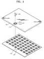
- FIG. 1illustrates a schematic perspective view of a method of aligning a substrate having a treatment region according to an embodiment of the present invention
- FIG. 2illustrates a conceptional cross-sectional view of forming the treatment region illustrated in FIG. 1 ;
- FIG. 3illustrates a cross-sectional view of a treatment region formed by etching according to an embodiment of the present invention
- FIG. 4illustrates a cross-sectional view of a treatment region formed by melting according to an embodiment of the present invention
- FIG. 5illustrates a plan view of a substrate and a mask aligned according to the alignment method illustrated in FIG. 1 ;
- FIG. 6illustrates a schematic cross-sectional view of a flat display apparatus having a substrate with a treatment region according to an embodiment of the present invention
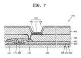
- FIG. 7illustrates a schematic cross-sectional view of an organic EL display device according to an embodiment of the present invention
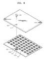
- FIG. 8illustrates a schematic perspective view of a method of aligning a substrate having a treatment region according to another embodiment of the present invention
- FIG. 9illustrates a conceptional cross-sectional view of forming the treatment region illustrated in FIG. 8 ;
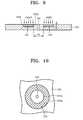
- FIGS. 10-11illustrate plan views of exemplary outer boundaries of the treatment region illustrated in FIG. 8 ;
- FIG. 12illustrates a cross-sectional view of a substrate and a mask aligned according to the alignment method illustrated in FIG. 8 ;
- FIG. 13illustrates a plan view of the substrate and mask illustrated in FIG. 12 .
- Korean Patent Application No. 10-2006-0046575filed on May 24, 2006, No. 10-2006-0067105, filed on Jul. 18, 2006, and No. 10-2006-0077822, filed on Aug. 17, 2006, in the Korean Intellectual Property Office, and entitled: “Method of Aligning Substrate and Flat Panel Display Apparatus Using the Same,” are incorporated by reference herein in their entirety.
- FIGS. 1-5an exemplary embodiment of a method of aligning a substrate and a mask according to the present invention will be described in more detail with reference to FIGS. 1-5 .
- a first alignment hole 210 with a treatment region 250may be formed in a substrate 200 .
- a mask 220 with a second alignment hole 230may be positioned below the substrate 200 , so that the first alignment hole 210 and the second alignment hole 230 may be substantially aligned.
- a sensor unit 240may be positioned above the first alignment hole 210 of the substrate 200 in order to determine proper alignment of the first and second alignment holes 210 and 230 .
- the substrate 200may be any suitable substrate employed in a flexible flat panel display device as determined by one of ordinary skill in the art.
- the substrate 200may be made of an opaque material, such as metal, e.g., steel use stainless (SUS).
- the first alignment hole 210may be formed through the substrate 200 and in close proximity to an edge thereof. In other words, the first alignment hole 210 may be formed sufficiently close to an edge of the substrate 200 to avoid an overlap between the treatment region 250 of the substrate 200 with any essential components of the flat panel display device. On the other hand, the first alignment hole 210 may be formed sufficiently far from the edge of the substrate 200 to avoid an overlap between the treatment region 250 with the edge of the substrate 200 .
- the first alignment hole 210may have a first width w 1 , as measured along a horizontal direction and illustrated in FIG. 2 , e.g., if the first alignment hole 210 has a circular shape, the first width w 1 may equal a diameter of the first alignment hole 210 .
- the treatment region 250may be formed on an upper surface of the substrate 200 around the first alignment hole 210 .
- the treatment region 250may have a shape of a ring having an inner boundary 250 a and an outer boundary 250 b , so that the outer boundary 250 b may have a larger width than the inner boundary 250 a .
- the first alignment hole 210 of the substrate 200may be concentric to the inner boundary 250 a , and the inner boundary 250 a of the treatment region 250 may be in communication with an edge of the first alignment hole 210 .
- the treatment region 250may be formed to exhibit a substantially different surface reflectance as compared to a surface reflectance of the substrate 200 .
- the substantially different surface reflectancerefers to a difference in reflectance capable of being detected by a standard optical sensor as may be used by one of ordinary skill in the art, e.g., a charged coupled device (CCD) camera.
- the surface reflectancemay be modified by a laser beam of a laser ablation device. For example, as illustrated in FIG.
- an area surrounding the first alignment hole 210may be irradiated to modify a surface texture thereof, e.g., visually and/or physically, to form the treatment region 250 with a second width w 2 and a rougher surface texture as compared to a surface texture of the substrate 200 , i.e., a higher average roughness values with respect to height of bumps on a surface.
- the treatment region 250 formed by the laser beammay also have a surface color that is different from the color of the substrate 200 .
- the substrate 200may be etched to a predetermined thickness to form the treatment region 250 .
- the laser beam intensitymay be adjusted to remove portions from the substrate 200 , so the treatment region 250 may have a thickness t, i.e., a vertical distance as measured in a downward direction from an upper surface of the substrate 200 that is lower than a thickness of the substrate 200 .
- the thickness t of the treatment region 250may equal half a thickness of the substrate 200 .
- the thickness tmay be in the range of about 30 ⁇ m to about 100 ⁇ m.
- the thickness t of the irradiation region 250may be controlled by adjusting the intensity of the laser beam of the laser ablation device or by using a mask.
- the treatment region 250may further have the second width w 2 , i.e., a horizontal distance as measured between the inner and outer boundaries 250 a and 250 b , having a value of about 1 mm or less.
- the substrate 200may be heat treated by a laser beam to form the treatment region 250 .
- the intensity of the laser beammay be adjusted to partially melt the upper surface of the substrate 200 to the thickness t and the second width w 2 .
- the thickness t and second width w 2 of the treatment region 250 formed by surface meltingmay be similar to the thickness t and second width w 2 of the treatment region 250 formed by surface etching.
- the color and roughness of the surface of the treatment region 250 formed by heat treatmentmay be different as compared to the substrate 200 .
- the surface of the treatment region 250 formed by meltingmay be darker as compared to the substrate 200 .
- the treatment region 250may facilitate optical distinction therebetween.
- the increased surface roughness in the treatment region 250may provide different reflectance as compared to the reflectance of the substrate 200 .
- Different reflectance valuesmay facilitate improved optical detection of a boundary line between the treatment region 250 and the substrate 200 and, thereby, enable location of the first alignment hole 210 with respect to a center of the treatment region 250 .
- the mask 220 positioned below the substrate 200may be made of metal, e.g., nickel or stainless steel, and may include a predetermined pattern to be imparted to a film deposited on the substrate 200 .
- the predetermined patternmay be formed in the mask 220 , e.g., by etching.
- the second alignment hole 230may be formed through the mask 220 , e.g., by punching.
- the second alignment hole 230may have a third width w 3 , as illustrated in FIG. 5 , that is smaller than the first alignment hole 210 . It is believed that different widths of the first and second alignment holes 210 and 230 may facilitate optical recognition of each of the first and second alignment holes 210 and 230 . It should be noted, however, that other types and configurations of masks for depositing a pattern on the substrate 200 are not excluded from the scope of the present invention.
- the sensor unit 240may be disposed above the upper surface of the substrate 200 , so that the substrate 200 may be positioned between the sensor unit 240 and the mask 220 . More specifically, the sensor unit 240 may be positioned directly above the first alignment hole 210 , and may include a camera, e.g., a CCD, to check alignment between the substrate 200 and the mask 220 , i.e., alignment between the first and second alignment holes 210 and 230 . Proper alignment between the first and second alignment holes 210 and 230 may vertically line up centers of the first and second alignment holes 210 and 230 , so that the second alignment hole 230 may be seen through the first alignment hole 210 due to the difference of widths thereof.
- a camerae.g., a CCD
- the treatment region 250may surround the first alignment hole 210 of the substrate 200 , while the second alignment hole 230 may be seen through the first alignment hole 210 . Accordingly, proper alignment of the first and second alignment holes 210 and 230 may enable the sensor unit 240 to capture and display an image of the first and second alignment holes 210 and 230 . Further, the different surface reflectance of the treatment region 250 as compared to the substrate 200 may facilitate proper visual identification of the first alignment hole 210 in the image produced by the sensor unit 240 .
- Visual identification of the first alignment hole 210e.g., due to darker surface color of the irradiation region 250 , by the sensor unit 240 may provide a convenient method of confirming positioning of the second alignment hole 230 of the mask 220 with respect to the center of the first alignment hole 210 of the substrate 200 . Accordingly, the substrate 200 may be easily aligned with the mask 220 .
- a light display elementmay be mounted on the substrate 200 .
- a light display element 300may be deposited and patterned on an upper surface of the substrate 200 to form a flat display device 310 .
- the light display element 300may be a light emitting element, e.g., a light emitting diode, or a liquid crystal display element.
- an EL display devicemay be manufactured by, inter alia, aligning the substrate 200 with the mask 220 according to the embodiment described previously with respect to FIGS. 1-5 .
- an EL display device 400may include the substrate 200 and a light emitting element 470 on the substrate 200 .
- the EL display device 400depicts an active matrix (AM) light emitting display device with a thin film transistor (TFT).
- AMactive matrix
- TFTthin film transistor
- other types of light emitting display devicesare not excluded from the scope of the present invention.
- the EL display device 400may include a TFT on the substrate 200 and a buffer layer (not shown) formed as an insulator between the substrate 200 and the TFT. More specifically, a semiconductor layer 410 may be formed on the substrate 200 . Once the semiconductor layer 410 is formed, a gate insulating film 420 and a gate electrode 430 may be formed sequentially on the semiconductor layer 410 . Next, an interlayer insulating film 440 may be formed on the gate electrode 430 to coat the gate electrode 430 and the gate insulating film 420 .
- Contact holesmay be formed in the interlayer insulating film 440 and the gate insulating film 420 , so that upon formation of source/drain electrodes 450 on the interlayer insulating film, electrical contact may be established between the source/drain electrodes 450 and the semiconductor layer 410 .
- the TFT described aboveis a top-gate type TFT, other types of TFTs are not excluded from the scope of the present invention.
- the EL display device 400may further include a passivation film 460 on the TFT, the light emitting element 470 on the passivation film 460 , and a pixel defining film 465 to coat the passivation film 460 .
- the passivation film 460may be made of an inorganic and/or organic material, and may have a flat upper surface regardless of a curvature of a lower surface. Alternatively, the passivation film 460 may have a curved upper surface, so that a curvature of the upper surface may be identical to the curvature of the lower surface.
- the pixel defining film 465may be a non-continuous layer, so that an opening may be formed therein to expose a portion of the light emitting element 470 .
- the light emitting element 470 of the EL display device 400may include a pixel electrode 472 , a light emitting layer 474 , and an opposite electrode 476 .
- the pixel electrode 472may be formed on the passivation film 460 and be in electric communication with the drain electrode 450 of the TFT through a via hole in the passivation film 460 .
- the light emitting layer 474e.g., made of an organic material
- the opposite electrode 476may be sequentially deposited on the pixel electrode 472 , i.e., the pixel and opposite electrodes 472 and 476 may be separated from each other by the light emitting layer 474 .
- the pixel electrode 472may function as an anode electrode, and the opposite electrode 476 may function as a cathode electrode.
- the polarities of the pixel electrode 472 and the opposite electrode 476may be switched. Accordingly, voltage may be applied to the pixel and opposite electrodes 472 and 476 to trigger excitation of the light emitting layer 474 therebetween.
- the light emitting element 470may be hermetically sealed.
- the pixel electrode 472may be made of a material having a high work function, e.g., a transparent conductive material, such as indium-tin-oxide (ITO), indium-zinc-oxide (IZO), indium oxide (In 2 O 3 ), zinc oxide (ZnO), and so forth.
- the opposite electrode 476may include a metal having a low work function, e.g., silver (Ag), magnesium (Mg), aluminum (Al), platinum (Pt), palladium (Pd), gold (Au), nickel (Ni), neodymium (Nd), iridium (Ir), chromium (Cr), lithium (Li), calcium (Ca), or a combination thereof.
- the light emitting layer 474may be deposited by vacuum evaporation method, and may be made of a low molecular weight organic molecule or a polymer.
- a low molecular weight organic moleculee.g., copper phthalocyanine (CuPc), N,N′-di-(naphthalene-1-yl)-N,N′-diphenyl-benzidine (NPB), or tris-8-hydroxyquinoline aluminum (Alq3)
- a hole injection layer (HIL), a hole transport layer (HTL), a light emitting layer (EML), an electron transport layer (ETL), and an electron injection layer (EIL)may be formed therein in a single or a composite structure.
- the HIL, ETL and EIL of the light emitting layer 474may be used for depositing red, green and blue pixels. Accordingly, the light emitting layer 474 may be formed to coat the entire pixel defining film 465 (not shown).
- the light emitting layer 474may include a HTL and an EML.
- the HTLmay include, e.g., poly-3,4-ethylenedioxythiophene (PEDOT), and the EML may include, e.g., poly-phenylenevinylene (PPV) based material and/or a polyfluorene based material.
- PVpoly-phenylenevinylene
- the HTL and the EMLmay be formed by using a screen printing or an inkjet printing method. It should be noted, however, that other materials for forming the light emitting layer 474 are not excluded from the scope of the present invention.
- a method of aligning a substrate with a maskmay include formation of a first alignment hole 510 in a substrate 500 , formation of a second alignment hole 530 with a treatment region 535 in a mask 520 , and aligning the first and second alignment holes 510 and 530 , so that the sensor unit 240 may be positioned above the substrate 500 to determine proper alignment of the first and second alignment holes 510 and 530 .
- the mask 520 and the substrate 500are similar to the mask 220 and the substrate 200 described previously with respect to FIGS. 1-5 and, therefore, their description will not be repeated herein.
- formation of the respective first and second alignment holes, their size ratio, and locationare similar in both embodiment and, therefore, will not be repeated herein.
- the method illustrated in FIGS. 8-13is similar to the method illustrated in FIGS. 1-5 , with the exception that a treatment region is formed in the mask 520 and not in the substrate 500 .
- the treatment region 535may be formed on an upper surface of the mask 520 around the second alignment hole 530 , so that the second alignment hole 530 may be positioned in a center of the treatment region 535 .
- the treatment region 535may be formed to have a surface having a reflectance substantially different from a reflectance of the upper surface of the mask 520 .
- the treatment region 535may be formed by using a laser ablation device.
- a laser beammay be used to irradiate an area surrounding the second alignment hole 530 to form the treatment region 535 , so that the treatment region 535 may have a surface texture that is rougher than a surface texture of the mask 520 , i.e., a higher average roughness values with respect to height of bumps on a surface.
- the treatment region 530 formed by the laser beammay also have a surface color that is different from the color of the mask 520 .
- the treatment region 535may have the thickness t. The thickness t may be determined by one of ordinary skill in the art with respect to a material used to form the mask 520 , so that a strength of the mask 520 is not affected.
- the thickness tmay equal about half a thickness of the mask 520 .
- the thickness t of the treatment region 535may be formed by removing, i.e., etching, portions of the mask 520 , applying a mask, and so forth. Upon etching, an upper surface of the treatment region 535 may have a modified surface roughness as compared to the mask 520 .
- the mask 520may be heat treated by the laser beam to form the treatment region 535 .
- the intensity of the laser beammay be increased to partially melt the upper surface of the mask 520 to the thickness t.
- the thickness t and surface roughness of the treatment region 535 formed by surface meltingmay be similar to the thickness t of the treatment region 535 formed by surface etching.
- the treatment region 535may have a shape of a ring having an inner boundary 535 a and an outer boundary 535 b , so that the second alignment hole 530 of the mask 520 may be concentric to the inner boundary 535 a .
- the outer boundary 535 bmay have a larger width than the inner boundary 535 a , so that the treatment region 535 may have a width corresponding to a horizontal distance as measured between the inner and outer boundaries 535 a and 535 b .
- the treatment region 535should be spaced apart from the second alignment hole 530 , i.e., the inner boundary 535 a of the treatment region 535 should be positioned at a predetermined distance from the interface between the second alignment hole 530 and the mask 520 . If the inner boundary 535 a of the treatment region 535 overlaps with the interface between the second alignment hole 530 and the mask 520 , i.e., the inner boundary 535 a is in communication with the second alignment hole 530 , it may be difficult to distinguish the second alignment hole 530 and the treatment region 535 from each other in images produced by the sensor unit 240 due to low reflectance difference therebetween. In other words, the sensor unit 240 may not identify the second alignment hole 530 and/or confirm alignment between the first and second alignment holes 510 and 530 and, thereby, fail to facilitate alignment between the substrate 500 and the mask 520 .
- the inner boundary 535 amay have a fourth width w 4 that is larger than a third width w 3 of the second alignment hole 530 and smaller than a first width w 1 of the first alignment hole 510 .
- the fourth width w 4 of the inner boundary 535 amay be smaller than the first width of the first alignment hole 510 to allow the treatment region 535 to be seen through the sensor unit 240 .
- the outer boundary 535 bmay have a width that is larger than the first width w 1 to facilitate detection of the first alignment hole 510 of the substrate 500 through the sensor unit 240 upon alignment of the substrate 500 with the mask 520 .
- the outer boundary 535 b of the treatment region 535may be formed in any shape as determined by one of ordinary skill in the art as long as its width is larger than the first width w 1 of the first alignment hole 510 upon alignment of the first and second alignment holes 510 and 530 .
- the outer boundary 535 b of the treatment region 535may have a circular perimeter, as illustrated in FIG. 10 .
- the outer boundary 535 b of the treatment region 535may have a rectangular perimeter, as illustrated in FIG. 11 .
- the outer boundary 535 b of the treatment region 535may not be seen through the first alignment hole 530 upon alignment of the substrate 500 and the mask 520 , as illustrated in FIG.
- a portion of the treatment region 535 within the first width w 1 of the first alignment hole 510may be seen through the first alignment hole 510 and, therefore, be displayed via the sensor unit 240 .
- the portion of the treatment region 535 exposed through the first alignment hole 510may be aligned with the first alignment hole 510 and facilitate visual distinction therebetween.
- the treatment region 535may be formed by metal deposition onto the mask 520 . More specifically, any mental having a higher reflectance as compared to the mask 520 , e.g., aluminum (Ag), silver (Ag), chromium (Cr), platinum (Pt), or an alloy thereof, may be used. Alternatively, the treatment region 535 may be formed via chemical mechanical polishing (CMP). In yet another alternative, the treatment region 535 may be formed using sand blasting, so that the surface roughness of the treatment region 535 may be increased by jetting sand under a high pressure. When the treatment region 535 is formed via metal deposition or CMP, the reflectance of the treatment region 535 may be higher than the reflectance of the surface of the mask 520 . Accordingly, the treatment region 535 may appear as a brighter region as compared to the mask 520 when viewed via the sensor unit 240 and, therefore, facilitate alignment of the substrate 500 with the mask 520 .
- CMPchemical mechanical polishing
Landscapes
- Physics & Mathematics (AREA)
- General Physics & Mathematics (AREA)
- Engineering & Computer Science (AREA)
- Multimedia (AREA)
- Life Sciences & Earth Sciences (AREA)
- Sustainable Development (AREA)
- Electroluminescent Light Sources (AREA)
Abstract
Description
Claims (17)
Applications Claiming Priority (6)
| Application Number | Priority Date | Filing Date | Title |
|---|---|---|---|
| KR10-2006-0046575 | 2006-05-24 | ||
| KR1020060046575AKR100759698B1 (en) | 2006-05-24 | 2006-05-24 | Mask and Alignment Method of Conductive Substrate and Mask Using Same |
| KR1020060067105AKR101264329B1 (en) | 2006-07-18 | 2006-07-18 | Mask and method of aligning substrate using the same |
| KR10-2006-0067105 | 2006-07-18 | ||
| KR1020060077822AKR100846589B1 (en) | 2006-08-17 | 2006-08-17 | Board Alignment Method |
| KR10-2006-0077822 | 2006-08-17 |
Publications (2)
| Publication Number | Publication Date |
|---|---|
| US20070275497A1 US20070275497A1 (en) | 2007-11-29 |
| US7835001B2true US7835001B2 (en) | 2010-11-16 |
Family
ID=38750025
Family Applications (1)
| Application Number | Title | Priority Date | Filing Date |
|---|---|---|---|
| US11/802,323Active2028-08-15US7835001B2 (en) | 2006-05-24 | 2007-05-22 | Method of aligning a substrate, mask to be aligned with the same, and flat panel display apparatus using the same |
Country Status (1)
| Country | Link |
|---|---|
| US (1) | US7835001B2 (en) |
Cited By (4)
| Publication number | Priority date | Publication date | Assignee | Title |
|---|---|---|---|---|
| US20070262936A1 (en)* | 2006-05-09 | 2007-11-15 | Chang Jae-Hyuk | Apparatus for manufacturing display panel and method for manufacturing the same |
| US20140167619A1 (en)* | 2012-12-17 | 2014-06-19 | Apple Inc. | Light Sensors For Electronic Devices |
| US9024250B2 (en) | 2012-09-07 | 2015-05-05 | Apple Inc. | Electronic device with light sensor alignment structures |
| US10510959B2 (en)* | 2017-08-22 | 2019-12-17 | Wuhan China Star Optoelectronics Semiconductor Display Technology Co., Ltd. | Commissioning method and vapor deposition machine |
Families Citing this family (43)
| Publication number | Priority date | Publication date | Assignee | Title |
|---|---|---|---|---|
| JP5328726B2 (en) | 2009-08-25 | 2013-10-30 | 三星ディスプレイ株式會社 | Thin film deposition apparatus and organic light emitting display device manufacturing method using the same |
| JP5677785B2 (en)* | 2009-08-27 | 2015-02-25 | 三星ディスプレイ株式會社Samsung Display Co.,Ltd. | Thin film deposition apparatus and organic light emitting display device manufacturing method using the same |
| JP5611718B2 (en)* | 2009-08-27 | 2014-10-22 | 三星ディスプレイ株式會社Samsung Display Co.,Ltd. | Thin film deposition apparatus and organic light emitting display device manufacturing method using the same |
| US8876975B2 (en) | 2009-10-19 | 2014-11-04 | Samsung Display Co., Ltd. | Thin film deposition apparatus |
| KR101084184B1 (en) | 2010-01-11 | 2011-11-17 | 삼성모바일디스플레이주식회사 | Thin film deposition apparatus |
| KR101174875B1 (en) | 2010-01-14 | 2012-08-17 | 삼성디스플레이 주식회사 | Apparatus for thin layer deposition, method for manufacturing of organic light emitting display apparatus using the same, and organic light emitting display apparatus manufactured by the method |
| KR101193186B1 (en) | 2010-02-01 | 2012-10-19 | 삼성디스플레이 주식회사 | Apparatus for thin layer deposition, method for manufacturing of organic light emitting display apparatus using the same, and organic light emitting display apparatus manufactured by the method |
| KR101156441B1 (en) | 2010-03-11 | 2012-06-18 | 삼성모바일디스플레이주식회사 | Apparatus for thin layer deposition |
| KR101202348B1 (en) | 2010-04-06 | 2012-11-16 | 삼성디스플레이 주식회사 | Apparatus for thin layer deposition and method for manufacturing of organic light emitting display apparatus using the same |
| US8894458B2 (en) | 2010-04-28 | 2014-11-25 | Samsung Display Co., Ltd. | Thin film deposition apparatus, method of manufacturing organic light-emitting display device by using the apparatus, and organic light-emitting display device manufactured by using the method |
| KR101223723B1 (en) | 2010-07-07 | 2013-01-18 | 삼성디스플레이 주식회사 | Apparatus for thin layer deposition, method for manufacturing of organic light emitting display apparatus using the same, and organic light emitting display apparatus manufactured by the method |
| KR101678056B1 (en) | 2010-09-16 | 2016-11-22 | 삼성디스플레이 주식회사 | Apparatus for thin layer deposition, method for manufacturing of organic light emitting display apparatus using the same, and organic light emitting display apparatus manufactured by the method |
| KR101738531B1 (en) | 2010-10-22 | 2017-05-23 | 삼성디스플레이 주식회사 | Method for manufacturing of organic light emitting display apparatus, and organic light emitting display apparatus manufactured by the method |
| KR101723506B1 (en) | 2010-10-22 | 2017-04-19 | 삼성디스플레이 주식회사 | Apparatus for organic layer deposition and method for manufacturing of organic light emitting display apparatus using the same |
| KR20120045865A (en) | 2010-11-01 | 2012-05-09 | 삼성모바일디스플레이주식회사 | Apparatus for organic layer deposition |
| KR20120065789A (en) | 2010-12-13 | 2012-06-21 | 삼성모바일디스플레이주식회사 | Apparatus for organic layer deposition |
| KR101760897B1 (en) | 2011-01-12 | 2017-07-25 | 삼성디스플레이 주식회사 | Deposition source and apparatus for organic layer deposition having the same |
| CN102134697A (en)* | 2011-01-19 | 2011-07-27 | 北京广微积电科技有限公司 | Mask plate and positioning method thereof |
| KR101923174B1 (en) | 2011-05-11 | 2018-11-29 | 삼성디스플레이 주식회사 | ESC, apparatus for thin layer deposition therewith, and method for manufacturing of organic light emitting display apparatus using the same |
| KR101852517B1 (en) | 2011-05-25 | 2018-04-27 | 삼성디스플레이 주식회사 | Apparatus for organic layer deposition and method for manufacturing of organic light emitting display apparatus using the same |
| KR101840654B1 (en) | 2011-05-25 | 2018-03-22 | 삼성디스플레이 주식회사 | Apparatus for organic layer deposition and method for manufacturing of organic light emitting display apparatus using the same |
| KR101857249B1 (en) | 2011-05-27 | 2018-05-14 | 삼성디스플레이 주식회사 | Patterning slit sheet assembly, apparatus for organic layer deposition, method for manufacturing organic light emitting display apparatus and organic light emitting display apparatus |
| KR101826068B1 (en) | 2011-07-04 | 2018-02-07 | 삼성디스플레이 주식회사 | Apparatus for thin layer deposition |
| KR20130004830A (en) | 2011-07-04 | 2013-01-14 | 삼성디스플레이 주식회사 | Apparatus for thin layer deposition and method for manufacturing of organic light emitting display apparatus using the same |
| KR20130069037A (en) | 2011-12-16 | 2013-06-26 | 삼성디스플레이 주식회사 | Apparatus for thin layer deposition, method for manufacturing of organic light emitting display apparatus using the same, and organic light emitting display apparatus |
| KR101959974B1 (en) | 2012-07-10 | 2019-07-16 | 삼성디스플레이 주식회사 | Apparatus for organic layer deposition, method for manufacturing of organic light emitting display apparatus using the same, and organic light emitting display apparatus manufactured by the method |
| US9496524B2 (en) | 2012-07-10 | 2016-11-15 | Samsung Display Co., Ltd. | Organic layer deposition apparatus, method of manufacturing organic light-emitting display apparatus using the same, and organic light-emitting display apparatus manufactured using the method |
| KR20140017767A (en) | 2012-07-31 | 2014-02-12 | 삼성디스플레이 주식회사 | Mask for deposition and method for aligning the same |
| JP2014053343A (en)* | 2012-09-05 | 2014-03-20 | Toyota Motor Corp | Semiconductor positioning device, and semiconductor positioning method |
| KR102013318B1 (en) | 2012-09-20 | 2019-08-23 | 삼성디스플레이 주식회사 | Apparatus for thin layer deposition, method for manufacturing of organic light emitting display apparatus using the same, and organic light emitting display apparatus |
| KR102081284B1 (en) | 2013-04-18 | 2020-02-26 | 삼성디스플레이 주식회사 | Deposition apparatus, method for manufacturing organic light emitting display apparatus using the same, and organic light emitting display apparatus manufactured by the same |
| KR102108361B1 (en) | 2013-06-24 | 2020-05-11 | 삼성디스플레이 주식회사 | Apparatus for monitoring deposition rate, apparatus for organic layer deposition using the same, method for monitoring deposition rate, and method for manufacturing of organic light emitting display apparatus using the same |
| JP6127834B2 (en)* | 2013-08-27 | 2017-05-17 | トヨタ自動車株式会社 | Alignment method and patterning mask |
| KR102162797B1 (en) | 2013-12-23 | 2020-10-08 | 삼성디스플레이 주식회사 | Method for manufacturing of organic light emitting display apparatus |
| JP6424521B2 (en)* | 2014-09-03 | 2018-11-21 | 大日本印刷株式会社 | Vapor deposition mask, vapor deposition mask with frame, and method of manufacturing organic semiconductor device |
| EP3993075A1 (en)* | 2015-04-24 | 2022-05-04 | Lg Innotek Co. Ltd | Deposition mask |
| CN104900630B (en)* | 2015-06-07 | 2018-01-26 | 上海华虹宏力半导体制造有限公司 | Improve structure of alignment mark contrast and forming method thereof |
| US9735185B1 (en) | 2016-06-10 | 2017-08-15 | Essential Products, Inc. | Hollowed electronic display |
| KR101893309B1 (en)* | 2017-10-31 | 2018-08-29 | 캐논 톡키 가부시키가이샤 | Alignment apparatus, alignment method, film forming apparatus, film forming method and manufacturing method of electronic device |
| CN108565359A (en)* | 2018-02-07 | 2018-09-21 | 上海瀚莅电子科技有限公司 | The alignment device and manufacturing system of silicon substrate OLED micro-displays |
| CN108441815A (en)* | 2018-04-10 | 2018-08-24 | 上海瀚莅电子科技有限公司 | The alignment device and manufacturing system of silicon substrate OLED micro-displays |
| JP7194006B2 (en)* | 2018-12-18 | 2022-12-21 | キヤノントッキ株式会社 | Substrate mounting method, film forming method, film forming apparatus, and organic EL panel manufacturing system |
| KR102820491B1 (en)* | 2020-03-25 | 2025-06-13 | 삼성디스플레이 주식회사 | Photo mask, display device and manufacturing mathod thereof |
Citations (29)
| Publication number | Priority date | Publication date | Assignee | Title |
|---|---|---|---|---|
| US4052280A (en)* | 1975-11-06 | 1977-10-04 | Scm Corporation | Uv curing of polymerizable binders |
| US4176281A (en)* | 1977-05-20 | 1979-11-27 | Siemens Aktiengesellschaft | Method for adjusting a semiconductor disk relative to a radiation mask in x-ray photolithography |
| JPS6229139A (en) | 1985-07-31 | 1987-02-07 | Hitachi Ltd | Pattern transfer mask and usage method |
| US4964146A (en) | 1985-07-31 | 1990-10-16 | Hitachi, Ltd. | Pattern transistor mask and method of using the same |
| JPH0354814A (en) | 1990-02-13 | 1991-03-08 | Hitachi Ltd | Manufacture of semiconductor device |
| US5084131A (en)* | 1990-01-11 | 1992-01-28 | Matsushita Electric Industrial Co., Ltd. | Fabrication method for thin film electroluminescent panels |
| US5216404A (en)* | 1990-07-25 | 1993-06-01 | Matsushita Electric Industrial Co., Ltd. | Sic thin-film thermistor |
| US5242641A (en)* | 1991-07-15 | 1993-09-07 | Pacific Trinetics Corporation | Method for forming filled holes in multi-layer integrated circuit packages |
| US5908719A (en)* | 1996-11-27 | 1999-06-01 | Wisconsin Alumni Research Foundation | Radiation mask adapted to be aligned with a photoresist layer and method of making the same |
| US6087719A (en)* | 1997-04-25 | 2000-07-11 | Kabushiki Kaisha Toshiba | Chip for multi-chip semiconductor device and method of manufacturing the same |
| US6110595A (en)* | 1997-03-27 | 2000-08-29 | Somar Corporation | Anti-reflective film |
| US6194101B1 (en)* | 1998-03-24 | 2001-02-27 | Oki Electric Industry Co., Ltd. | Photomask, and process and apparatus for determining condition of photomask |
| JP2001085302A (en) | 1999-09-10 | 2001-03-30 | Toshiba Corp | Charged beam exposure mask, charged beam exposure apparatus, and charged beam exposure method |
| US6327034B1 (en)* | 1999-09-20 | 2001-12-04 | Rex Hoover | Apparatus for aligning two objects |
| US6362883B1 (en)* | 1995-09-28 | 2002-03-26 | Micron Technology, Inc. | Method and device for aligning substrates in flat panel displays |
| US6406988B1 (en)* | 1998-04-24 | 2002-06-18 | Amerasia International Technology, Inc. | Method of forming fine pitch interconnections employing magnetic masks |
| KR20030029697A (en)* | 2001-10-08 | 2003-04-16 | 엘지전자 주식회사 | Align mark and plasma display panel using the same |
| US6799826B2 (en)* | 2002-04-08 | 2004-10-05 | Lg Electronics Inc. | Device and method for fabricating display panel having ink-jet printing applied thereto |
| US20050105009A1 (en)* | 2003-10-07 | 2005-05-19 | American Panel Corporation, L.G. Philips Lcd | Flat panel display having an isolated EMI layer and integral heater and thermal sensors |
| US20050241754A1 (en)* | 2004-04-28 | 2005-11-03 | Junichiro Iri | Method for dicing wafer and process for manufacturing liquid-discharging head using the dicing method |
| KR20060005031A (en) | 2004-07-12 | 2006-01-17 | 엘지전자 주식회사 | Indoor unit of air conditioner |
| US20060027809A1 (en) | 2004-08-09 | 2006-02-09 | Hiroyuki Ogawa | Semiconductor device including semiconductor thin film, which is subjected to heat treatment to have alignment mark, crystallizing method for the semiconductor thin film, and crystallizing apparatus for the semiconductor thin film |
| US7031578B2 (en)* | 2000-10-11 | 2006-04-18 | Commissariate A L'energie Atomique | Method and device for passive alignment of optical waveguides and optoelectronic components and optical system using said device |
| US20060086321A1 (en)* | 2004-10-22 | 2006-04-27 | Advantech Global, Ltd | Substrate-to-mask alignment and securing system with temperature control for use in an automated shadow mask vacuum deposition process |
| KR20060071610A (en) | 2004-12-22 | 2006-06-27 | 동부일렉트로닉스 주식회사 | Focus Determination Method of Wafer Using an Alignment Laser |
| US20060158074A1 (en)* | 2005-01-20 | 2006-07-20 | Kang Tae-Kyoung | Plasma display apparatus and method of manufacturing same |
| US20070262936A1 (en)* | 2006-05-09 | 2007-11-15 | Chang Jae-Hyuk | Apparatus for manufacturing display panel and method for manufacturing the same |
| US20070290616A1 (en)* | 2006-06-16 | 2007-12-20 | Lg Electronics Inc. | Organic light emitting device and method of fabricating the same |
| US20080042929A1 (en)* | 2006-06-30 | 2008-02-21 | Ock Hee Kim | Flexible display and method for forming alignment key of the same |
- 2007
- 2007-05-22USUS11/802,323patent/US7835001B2/enactiveActive
Patent Citations (29)
| Publication number | Priority date | Publication date | Assignee | Title |
|---|---|---|---|---|
| US4052280A (en)* | 1975-11-06 | 1977-10-04 | Scm Corporation | Uv curing of polymerizable binders |
| US4176281A (en)* | 1977-05-20 | 1979-11-27 | Siemens Aktiengesellschaft | Method for adjusting a semiconductor disk relative to a radiation mask in x-ray photolithography |
| JPS6229139A (en) | 1985-07-31 | 1987-02-07 | Hitachi Ltd | Pattern transfer mask and usage method |
| US4964146A (en) | 1985-07-31 | 1990-10-16 | Hitachi, Ltd. | Pattern transistor mask and method of using the same |
| US5084131A (en)* | 1990-01-11 | 1992-01-28 | Matsushita Electric Industrial Co., Ltd. | Fabrication method for thin film electroluminescent panels |
| JPH0354814A (en) | 1990-02-13 | 1991-03-08 | Hitachi Ltd | Manufacture of semiconductor device |
| US5216404A (en)* | 1990-07-25 | 1993-06-01 | Matsushita Electric Industrial Co., Ltd. | Sic thin-film thermistor |
| US5242641A (en)* | 1991-07-15 | 1993-09-07 | Pacific Trinetics Corporation | Method for forming filled holes in multi-layer integrated circuit packages |
| US6362883B1 (en)* | 1995-09-28 | 2002-03-26 | Micron Technology, Inc. | Method and device for aligning substrates in flat panel displays |
| US5908719A (en)* | 1996-11-27 | 1999-06-01 | Wisconsin Alumni Research Foundation | Radiation mask adapted to be aligned with a photoresist layer and method of making the same |
| US6110595A (en)* | 1997-03-27 | 2000-08-29 | Somar Corporation | Anti-reflective film |
| US6087719A (en)* | 1997-04-25 | 2000-07-11 | Kabushiki Kaisha Toshiba | Chip for multi-chip semiconductor device and method of manufacturing the same |
| US6194101B1 (en)* | 1998-03-24 | 2001-02-27 | Oki Electric Industry Co., Ltd. | Photomask, and process and apparatus for determining condition of photomask |
| US6406988B1 (en)* | 1998-04-24 | 2002-06-18 | Amerasia International Technology, Inc. | Method of forming fine pitch interconnections employing magnetic masks |
| JP2001085302A (en) | 1999-09-10 | 2001-03-30 | Toshiba Corp | Charged beam exposure mask, charged beam exposure apparatus, and charged beam exposure method |
| US6327034B1 (en)* | 1999-09-20 | 2001-12-04 | Rex Hoover | Apparatus for aligning two objects |
| US7031578B2 (en)* | 2000-10-11 | 2006-04-18 | Commissariate A L'energie Atomique | Method and device for passive alignment of optical waveguides and optoelectronic components and optical system using said device |
| KR20030029697A (en)* | 2001-10-08 | 2003-04-16 | 엘지전자 주식회사 | Align mark and plasma display panel using the same |
| US6799826B2 (en)* | 2002-04-08 | 2004-10-05 | Lg Electronics Inc. | Device and method for fabricating display panel having ink-jet printing applied thereto |
| US20050105009A1 (en)* | 2003-10-07 | 2005-05-19 | American Panel Corporation, L.G. Philips Lcd | Flat panel display having an isolated EMI layer and integral heater and thermal sensors |
| US20050241754A1 (en)* | 2004-04-28 | 2005-11-03 | Junichiro Iri | Method for dicing wafer and process for manufacturing liquid-discharging head using the dicing method |
| KR20060005031A (en) | 2004-07-12 | 2006-01-17 | 엘지전자 주식회사 | Indoor unit of air conditioner |
| US20060027809A1 (en) | 2004-08-09 | 2006-02-09 | Hiroyuki Ogawa | Semiconductor device including semiconductor thin film, which is subjected to heat treatment to have alignment mark, crystallizing method for the semiconductor thin film, and crystallizing apparatus for the semiconductor thin film |
| US20060086321A1 (en)* | 2004-10-22 | 2006-04-27 | Advantech Global, Ltd | Substrate-to-mask alignment and securing system with temperature control for use in an automated shadow mask vacuum deposition process |
| KR20060071610A (en) | 2004-12-22 | 2006-06-27 | 동부일렉트로닉스 주식회사 | Focus Determination Method of Wafer Using an Alignment Laser |
| US20060158074A1 (en)* | 2005-01-20 | 2006-07-20 | Kang Tae-Kyoung | Plasma display apparatus and method of manufacturing same |
| US20070262936A1 (en)* | 2006-05-09 | 2007-11-15 | Chang Jae-Hyuk | Apparatus for manufacturing display panel and method for manufacturing the same |
| US20070290616A1 (en)* | 2006-06-16 | 2007-12-20 | Lg Electronics Inc. | Organic light emitting device and method of fabricating the same |
| US20080042929A1 (en)* | 2006-06-30 | 2008-02-21 | Ock Hee Kim | Flexible display and method for forming alignment key of the same |
Cited By (6)
| Publication number | Priority date | Publication date | Assignee | Title |
|---|---|---|---|---|
| US20070262936A1 (en)* | 2006-05-09 | 2007-11-15 | Chang Jae-Hyuk | Apparatus for manufacturing display panel and method for manufacturing the same |
| US8253941B2 (en)* | 2006-05-09 | 2012-08-28 | Samsung Electronics Co., Ltd. | Apparatus for manufacturing display panel and method for manufacturing the same |
| US9024250B2 (en) | 2012-09-07 | 2015-05-05 | Apple Inc. | Electronic device with light sensor alignment structures |
| US20140167619A1 (en)* | 2012-12-17 | 2014-06-19 | Apple Inc. | Light Sensors For Electronic Devices |
| US9046421B2 (en)* | 2012-12-17 | 2015-06-02 | Apple Inc. | Light sensors for electronic devices |
| US10510959B2 (en)* | 2017-08-22 | 2019-12-17 | Wuhan China Star Optoelectronics Semiconductor Display Technology Co., Ltd. | Commissioning method and vapor deposition machine |
Also Published As
| Publication number | Publication date |
|---|---|
| US20070275497A1 (en) | 2007-11-29 |
Similar Documents
| Publication | Publication Date | Title |
|---|---|---|
| US7835001B2 (en) | Method of aligning a substrate, mask to be aligned with the same, and flat panel display apparatus using the same | |
| US10686156B2 (en) | Organic light emitting display device with auxiliary electrode and conductive member and method of fabricating the same | |
| US8866162B2 (en) | Organic light emitting diode display and method of manufacturing the same | |
| US8746169B2 (en) | Mask frame assembly for thin film deposition | |
| US9048454B2 (en) | Organic light emitting display apparatus and method of manufacturing the same | |
| US9035330B2 (en) | Organic light-emitting display device and method of manufacturing the organic light emitting display device | |
| US8518285B2 (en) | Substrate section for flexible display device, method of manufacturing the substrate section, and method of manufacturing organic light emitting display device including the substrate | |
| US8461591B2 (en) | Organic light emitting display apparatus and method of manufacturing the same | |
| US20150280166A1 (en) | Organic light-emitting display apparatus and manufacturing method thereof | |
| US20150027367A1 (en) | Mask frame assembly for thin film deposition | |
| JP2018026344A (en) | Mask assembly, display device manufacturing apparatus, display device manufacturing method, and display device | |
| US20170133592A1 (en) | Mask frame assembly, device for deposition including the same, and method of manufacturing display device | |
| US10923555B2 (en) | Organic light-emitting display apparatus | |
| US20170352712A1 (en) | Organic light-emitting display apparatus and method of manufacturing the same | |
| JP2011151017A (en) | Organic light-emitting display device, and manufacturing method thereof | |
| KR20210120175A (en) | Mask assembly, apparatus for manufacturing a display apparatus, and method for manufacturing a display apparatus | |
| EP3460850B1 (en) | Display device having an auxiliary electrode | |
| KR20250112218A (en) | Method of manufacturing mask, mask manufacture by the same, and method of manufacturing display apparatus | |
| US9825251B2 (en) | Display apparatus comprising a seal portion having two different thicknesses | |
| US20220006015A1 (en) | Apparatus and method of manufacturing display apparatus | |
| KR20150019392A (en) | Organic light emitting display apparatus and method for manufacturing the same | |
| KR101243924B1 (en) | Organic light emitting display apparatus | |
| US10833288B2 (en) | Display apparatus | |
| US9230869B2 (en) | Flexible organic light-emitting display apparatus and method of manufacturing the same | |
| KR100846589B1 (en) | Board Alignment Method |
Legal Events
| Date | Code | Title | Description |
|---|---|---|---|
| AS | Assignment | Owner name:SAMSUNG SDI CO., LTD., KOREA, REPUBLIC OF Free format text:ASSIGNMENT OF ASSIGNORS INTEREST;ASSIGNORS:KWACK, JIN-HO;AHN, TAE-KYUNG;KIM, MIN-KYU;AND OTHERS;REEL/FRAME:019392/0754 Effective date:20070510 | |
| AS | Assignment | Owner name:SAMSUNG MOBILE DISPLAY CO., LTD., KOREA, REPUBLIC OF Free format text:ASSIGNMENT OF ASSIGNORS INTEREST;ASSIGNOR:SAMSUNG SDI CO., LTD.;REEL/FRAME:021998/0771 Effective date:20081212 Owner name:SAMSUNG MOBILE DISPLAY CO., LTD., KOREA, REPUBLIC Free format text:ASSIGNMENT OF ASSIGNORS INTEREST;ASSIGNOR:SAMSUNG SDI CO., LTD.;REEL/FRAME:021998/0771 Effective date:20081212 Owner name:SAMSUNG MOBILE DISPLAY CO., LTD.,KOREA, REPUBLIC O Free format text:ASSIGNMENT OF ASSIGNORS INTEREST;ASSIGNOR:SAMSUNG SDI CO., LTD.;REEL/FRAME:021998/0771 Effective date:20081212 | |
| STCF | Information on status: patent grant | Free format text:PATENTED CASE | |
| FEPP | Fee payment procedure | Free format text:PAYOR NUMBER ASSIGNED (ORIGINAL EVENT CODE: ASPN); ENTITY STATUS OF PATENT OWNER: LARGE ENTITY | |
| AS | Assignment | Owner name:SAMSUNG DISPLAY CO., LTD., KOREA, REPUBLIC OF Free format text:MERGER;ASSIGNOR:SAMSUNG MOBILE DISPLAY CO., LTD.;REEL/FRAME:029096/0174 Effective date:20120827 | |
| FEPP | Fee payment procedure | Free format text:PAYER NUMBER DE-ASSIGNED (ORIGINAL EVENT CODE: RMPN); ENTITY STATUS OF PATENT OWNER: LARGE ENTITY Free format text:PAYOR NUMBER ASSIGNED (ORIGINAL EVENT CODE: ASPN); ENTITY STATUS OF PATENT OWNER: LARGE ENTITY | |
| FPAY | Fee payment | Year of fee payment:4 | |
| MAFP | Maintenance fee payment | Free format text:PAYMENT OF MAINTENANCE FEE, 8TH YEAR, LARGE ENTITY (ORIGINAL EVENT CODE: M1552) Year of fee payment:8 | |
| MAFP | Maintenance fee payment | Free format text:PAYMENT OF MAINTENANCE FEE, 12TH YEAR, LARGE ENTITY (ORIGINAL EVENT CODE: M1553); ENTITY STATUS OF PATENT OWNER: LARGE ENTITY Year of fee payment:12 |