US7833881B2 - Methods for fabricating semiconductor components and packaged semiconductor components - Google Patents
Methods for fabricating semiconductor components and packaged semiconductor componentsDownload PDFInfo
- Publication number
- US7833881B2 US7833881B2US11/681,648US68164807AUS7833881B2US 7833881 B2US7833881 B2US 7833881B2US 68164807 AUS68164807 AUS 68164807AUS 7833881 B2US7833881 B2US 7833881B2
- Authority
- US
- United States
- Prior art keywords
- trenches
- wafer
- protective material
- cutting
- lanes
- Prior art date
- Legal status (The legal status is an assumption and is not a legal conclusion. Google has not performed a legal analysis and makes no representation as to the accuracy of the status listed.)
- Active, expires
Links
- 239000004065semiconductorSubstances0.000titleclaimsabstractdescription73
- 238000000034methodMethods0.000titleclaimsabstractdescription72
- 238000004519manufacturing processMethods0.000claimsabstractdescription13
- 239000000463materialSubstances0.000claimsdescription85
- 230000001681protective effectEffects0.000claimsdescription61
- 238000005520cutting processMethods0.000claimsdescription30
- 238000000151depositionMethods0.000claimsdescription15
- 238000000465mouldingMethods0.000claimsdescription9
- 239000000945fillerSubstances0.000claimsdescription4
- 238000000227grindingMethods0.000claimsdescription3
- 239000013047polymeric layerSubstances0.000claims1
- 238000007373indentationMethods0.000abstractdescription10
- 239000000758substrateSubstances0.000abstractdescription9
- 235000012431wafersNutrition0.000description82
- 238000003491arrayMethods0.000description6
- 229910052751metalInorganic materials0.000description5
- 239000002184metalSubstances0.000description5
- 238000005530etchingMethods0.000description4
- 238000004806packaging method and processMethods0.000description4
- 229910000679solderInorganic materials0.000description4
- 150000002739metalsChemical class0.000description3
- 238000005382thermal cyclingMethods0.000description3
- 239000004593EpoxySubstances0.000description2
- PXHVJJICTQNCMI-UHFFFAOYSA-NNickelChemical compound[Ni]PXHVJJICTQNCMI-UHFFFAOYSA-N0.000description2
- KDLHZDBZIXYQEI-UHFFFAOYSA-NPalladiumChemical compound[Pd]KDLHZDBZIXYQEI-UHFFFAOYSA-N0.000description2
- 239000004642PolyimideSubstances0.000description2
- 238000005538encapsulationMethods0.000description2
- PCHJSUWPFVWCPO-UHFFFAOYSA-NgoldChemical compound[Au]PCHJSUWPFVWCPO-UHFFFAOYSA-N0.000description2
- 229910052737goldInorganic materials0.000description2
- 239000010931goldSubstances0.000description2
- 238000012858packaging processMethods0.000description2
- BASFCYQUMIYNBI-UHFFFAOYSA-NplatinumChemical compound[Pt]BASFCYQUMIYNBI-UHFFFAOYSA-N0.000description2
- 229920001721polyimidePolymers0.000description2
- 229920001296polysiloxanePolymers0.000description2
- RYGMFSIKBFXOCR-UHFFFAOYSA-NCopperChemical compound[Cu]RYGMFSIKBFXOCR-UHFFFAOYSA-N0.000description1
- BQCADISMDOOEFD-UHFFFAOYSA-NSilverChemical compound[Ag]BQCADISMDOOEFD-UHFFFAOYSA-N0.000description1
- ATJFFYVFTNAWJD-UHFFFAOYSA-NTinChemical compound[Sn]ATJFFYVFTNAWJD-UHFFFAOYSA-N0.000description1
- HCHKCACWOHOZIP-UHFFFAOYSA-NZincChemical compound[Zn]HCHKCACWOHOZIP-UHFFFAOYSA-N0.000description1
- 229910045601alloyInorganic materials0.000description1
- 239000000956alloySubstances0.000description1
- 238000005452bendingMethods0.000description1
- 230000015572biosynthetic processEffects0.000description1
- 230000001413cellular effectEffects0.000description1
- 238000004891communicationMethods0.000description1
- 229920001940conductive polymerPolymers0.000description1
- 230000008602contractionEffects0.000description1
- 229910052802copperInorganic materials0.000description1
- 239000010949copperSubstances0.000description1
- 238000005336crackingMethods0.000description1
- 238000013500data storageMethods0.000description1
- 230000003247decreasing effectEffects0.000description1
- 238000005137deposition processMethods0.000description1
- 238000001312dry etchingMethods0.000description1
- 239000012776electronic materialSubstances0.000description1
- 230000007613environmental effectEffects0.000description1
- 230000006870functionEffects0.000description1
- 238000003384imaging methodMethods0.000description1
- 238000003698laser cuttingMethods0.000description1
- 238000003754machiningMethods0.000description1
- 230000005055memory storageEffects0.000description1
- 238000004377microelectronicMethods0.000description1
- 238000012986modificationMethods0.000description1
- 230000004048modificationEffects0.000description1
- 229910052759nickelInorganic materials0.000description1
- 229910052763palladiumInorganic materials0.000description1
- 238000001020plasma etchingMethods0.000description1
- 229910052697platinumInorganic materials0.000description1
- 229920000642polymerPolymers0.000description1
- 239000002861polymer materialSubstances0.000description1
- 238000012545processingMethods0.000description1
- 230000005855radiationEffects0.000description1
- 238000007650screen-printingMethods0.000description1
- 238000000926separation methodMethods0.000description1
- 150000004760silicatesChemical class0.000description1
- 229910052709silverInorganic materials0.000description1
- 239000004332silverSubstances0.000description1
- 238000005476solderingMethods0.000description1
- 230000003068static effectEffects0.000description1
- 238000003860storageMethods0.000description1
- 238000012360testing methodMethods0.000description1
- 229910052718tinInorganic materials0.000description1
- 239000011135tinSubstances0.000description1
- 238000001039wet etchingMethods0.000description1
- 229910052725zincInorganic materials0.000description1
- 239000011701zincSubstances0.000description1
Images


Classifications
- H—ELECTRICITY
- H01—ELECTRIC ELEMENTS
- H01L—SEMICONDUCTOR DEVICES NOT COVERED BY CLASS H10
- H01L21/00—Processes or apparatus adapted for the manufacture or treatment of semiconductor or solid state devices or of parts thereof
- H01L21/02—Manufacture or treatment of semiconductor devices or of parts thereof
- H01L21/04—Manufacture or treatment of semiconductor devices or of parts thereof the devices having potential barriers, e.g. a PN junction, depletion layer or carrier concentration layer
- H01L21/50—Assembly of semiconductor devices using processes or apparatus not provided for in a single one of the groups H01L21/18 - H01L21/326 or H10D48/04 - H10D48/07 e.g. sealing of a cap to a base of a container
- H01L21/56—Encapsulations, e.g. encapsulation layers, coatings
- H01L21/561—Batch processing
- H—ELECTRICITY
- H01—ELECTRIC ELEMENTS
- H01L—SEMICONDUCTOR DEVICES NOT COVERED BY CLASS H10
- H01L21/00—Processes or apparatus adapted for the manufacture or treatment of semiconductor or solid state devices or of parts thereof
- H01L21/70—Manufacture or treatment of devices consisting of a plurality of solid state components formed in or on a common substrate or of parts thereof; Manufacture of integrated circuit devices or of parts thereof
- H01L21/77—Manufacture or treatment of devices consisting of a plurality of solid state components or integrated circuits formed in, or on, a common substrate
- H01L21/78—Manufacture or treatment of devices consisting of a plurality of solid state components or integrated circuits formed in, or on, a common substrate with subsequent division of the substrate into plural individual devices
- H—ELECTRICITY
- H01—ELECTRIC ELEMENTS
- H01L—SEMICONDUCTOR DEVICES NOT COVERED BY CLASS H10
- H01L23/00—Details of semiconductor or other solid state devices
- H01L23/28—Encapsulations, e.g. encapsulating layers, coatings, e.g. for protection
- H01L23/31—Encapsulations, e.g. encapsulating layers, coatings, e.g. for protection characterised by the arrangement or shape
- H01L23/3157—Partial encapsulation or coating
- H—ELECTRICITY
- H01—ELECTRIC ELEMENTS
- H01L—SEMICONDUCTOR DEVICES NOT COVERED BY CLASS H10
- H01L2224/00—Indexing scheme for arrangements for connecting or disconnecting semiconductor or solid-state bodies and methods related thereto as covered by H01L24/00
- H01L2224/01—Means for bonding being attached to, or being formed on, the surface to be connected, e.g. chip-to-package, die-attach, "first-level" interconnects; Manufacturing methods related thereto
- H01L2224/02—Bonding areas; Manufacturing methods related thereto
- H01L2224/04—Structure, shape, material or disposition of the bonding areas prior to the connecting process
- H01L2224/05—Structure, shape, material or disposition of the bonding areas prior to the connecting process of an individual bonding area
- H01L2224/0554—External layer
- H01L2224/0556—Disposition
- H01L2224/05568—Disposition the whole external layer protruding from the surface
- H—ELECTRICITY
- H01—ELECTRIC ELEMENTS
- H01L—SEMICONDUCTOR DEVICES NOT COVERED BY CLASS H10
- H01L2224/00—Indexing scheme for arrangements for connecting or disconnecting semiconductor or solid-state bodies and methods related thereto as covered by H01L24/00
- H01L2224/01—Means for bonding being attached to, or being formed on, the surface to be connected, e.g. chip-to-package, die-attach, "first-level" interconnects; Manufacturing methods related thereto
- H01L2224/02—Bonding areas; Manufacturing methods related thereto
- H01L2224/04—Structure, shape, material or disposition of the bonding areas prior to the connecting process
- H01L2224/05—Structure, shape, material or disposition of the bonding areas prior to the connecting process of an individual bonding area
- H01L2224/0554—External layer
- H01L2224/05573—Single external layer
- H—ELECTRICITY
- H01—ELECTRIC ELEMENTS
- H01L—SEMICONDUCTOR DEVICES NOT COVERED BY CLASS H10
- H01L2224/00—Indexing scheme for arrangements for connecting or disconnecting semiconductor or solid-state bodies and methods related thereto as covered by H01L24/00
- H01L2224/01—Means for bonding being attached to, or being formed on, the surface to be connected, e.g. chip-to-package, die-attach, "first-level" interconnects; Manufacturing methods related thereto
- H01L2224/02—Bonding areas; Manufacturing methods related thereto
- H01L2224/04—Structure, shape, material or disposition of the bonding areas prior to the connecting process
- H01L2224/05—Structure, shape, material or disposition of the bonding areas prior to the connecting process of an individual bonding area
- H01L2224/0554—External layer
- H01L2224/05599—Material
- H01L2224/056—Material with a principal constituent of the material being a metal or a metalloid, e.g. boron [B], silicon [Si], germanium [Ge], arsenic [As], antimony [Sb], tellurium [Te] and polonium [Po], and alloys thereof
- H01L2224/05601—Material with a principal constituent of the material being a metal or a metalloid, e.g. boron [B], silicon [Si], germanium [Ge], arsenic [As], antimony [Sb], tellurium [Te] and polonium [Po], and alloys thereof the principal constituent melting at a temperature of less than 400°C
- H01L2224/05611—Tin [Sn] as principal constituent
- H—ELECTRICITY
- H01—ELECTRIC ELEMENTS
- H01L—SEMICONDUCTOR DEVICES NOT COVERED BY CLASS H10
- H01L2224/00—Indexing scheme for arrangements for connecting or disconnecting semiconductor or solid-state bodies and methods related thereto as covered by H01L24/00
- H01L2224/01—Means for bonding being attached to, or being formed on, the surface to be connected, e.g. chip-to-package, die-attach, "first-level" interconnects; Manufacturing methods related thereto
- H01L2224/02—Bonding areas; Manufacturing methods related thereto
- H01L2224/04—Structure, shape, material or disposition of the bonding areas prior to the connecting process
- H01L2224/05—Structure, shape, material or disposition of the bonding areas prior to the connecting process of an individual bonding area
- H01L2224/0554—External layer
- H01L2224/05599—Material
- H01L2224/056—Material with a principal constituent of the material being a metal or a metalloid, e.g. boron [B], silicon [Si], germanium [Ge], arsenic [As], antimony [Sb], tellurium [Te] and polonium [Po], and alloys thereof
- H01L2224/05617—Material with a principal constituent of the material being a metal or a metalloid, e.g. boron [B], silicon [Si], germanium [Ge], arsenic [As], antimony [Sb], tellurium [Te] and polonium [Po], and alloys thereof the principal constituent melting at a temperature of greater than or equal to 400°C and less than 950°C
- H01L2224/05618—Zinc [Zn] as principal constituent
- H—ELECTRICITY
- H01—ELECTRIC ELEMENTS
- H01L—SEMICONDUCTOR DEVICES NOT COVERED BY CLASS H10
- H01L2224/00—Indexing scheme for arrangements for connecting or disconnecting semiconductor or solid-state bodies and methods related thereto as covered by H01L24/00
- H01L2224/01—Means for bonding being attached to, or being formed on, the surface to be connected, e.g. chip-to-package, die-attach, "first-level" interconnects; Manufacturing methods related thereto
- H01L2224/02—Bonding areas; Manufacturing methods related thereto
- H01L2224/04—Structure, shape, material or disposition of the bonding areas prior to the connecting process
- H01L2224/05—Structure, shape, material or disposition of the bonding areas prior to the connecting process of an individual bonding area
- H01L2224/0554—External layer
- H01L2224/05599—Material
- H01L2224/056—Material with a principal constituent of the material being a metal or a metalloid, e.g. boron [B], silicon [Si], germanium [Ge], arsenic [As], antimony [Sb], tellurium [Te] and polonium [Po], and alloys thereof
- H01L2224/05638—Material with a principal constituent of the material being a metal or a metalloid, e.g. boron [B], silicon [Si], germanium [Ge], arsenic [As], antimony [Sb], tellurium [Te] and polonium [Po], and alloys thereof the principal constituent melting at a temperature of greater than or equal to 950°C and less than 1550°C
- H01L2224/05639—Silver [Ag] as principal constituent
- H—ELECTRICITY
- H01—ELECTRIC ELEMENTS
- H01L—SEMICONDUCTOR DEVICES NOT COVERED BY CLASS H10
- H01L2224/00—Indexing scheme for arrangements for connecting or disconnecting semiconductor or solid-state bodies and methods related thereto as covered by H01L24/00
- H01L2224/01—Means for bonding being attached to, or being formed on, the surface to be connected, e.g. chip-to-package, die-attach, "first-level" interconnects; Manufacturing methods related thereto
- H01L2224/02—Bonding areas; Manufacturing methods related thereto
- H01L2224/04—Structure, shape, material or disposition of the bonding areas prior to the connecting process
- H01L2224/05—Structure, shape, material or disposition of the bonding areas prior to the connecting process of an individual bonding area
- H01L2224/0554—External layer
- H01L2224/05599—Material
- H01L2224/056—Material with a principal constituent of the material being a metal or a metalloid, e.g. boron [B], silicon [Si], germanium [Ge], arsenic [As], antimony [Sb], tellurium [Te] and polonium [Po], and alloys thereof
- H01L2224/05638—Material with a principal constituent of the material being a metal or a metalloid, e.g. boron [B], silicon [Si], germanium [Ge], arsenic [As], antimony [Sb], tellurium [Te] and polonium [Po], and alloys thereof the principal constituent melting at a temperature of greater than or equal to 950°C and less than 1550°C
- H01L2224/05644—Gold [Au] as principal constituent
- H—ELECTRICITY
- H01—ELECTRIC ELEMENTS
- H01L—SEMICONDUCTOR DEVICES NOT COVERED BY CLASS H10
- H01L2224/00—Indexing scheme for arrangements for connecting or disconnecting semiconductor or solid-state bodies and methods related thereto as covered by H01L24/00
- H01L2224/01—Means for bonding being attached to, or being formed on, the surface to be connected, e.g. chip-to-package, die-attach, "first-level" interconnects; Manufacturing methods related thereto
- H01L2224/02—Bonding areas; Manufacturing methods related thereto
- H01L2224/04—Structure, shape, material or disposition of the bonding areas prior to the connecting process
- H01L2224/05—Structure, shape, material or disposition of the bonding areas prior to the connecting process of an individual bonding area
- H01L2224/0554—External layer
- H01L2224/05599—Material
- H01L2224/056—Material with a principal constituent of the material being a metal or a metalloid, e.g. boron [B], silicon [Si], germanium [Ge], arsenic [As], antimony [Sb], tellurium [Te] and polonium [Po], and alloys thereof
- H01L2224/05638—Material with a principal constituent of the material being a metal or a metalloid, e.g. boron [B], silicon [Si], germanium [Ge], arsenic [As], antimony [Sb], tellurium [Te] and polonium [Po], and alloys thereof the principal constituent melting at a temperature of greater than or equal to 950°C and less than 1550°C
- H01L2224/05647—Copper [Cu] as principal constituent
- H—ELECTRICITY
- H01—ELECTRIC ELEMENTS
- H01L—SEMICONDUCTOR DEVICES NOT COVERED BY CLASS H10
- H01L2224/00—Indexing scheme for arrangements for connecting or disconnecting semiconductor or solid-state bodies and methods related thereto as covered by H01L24/00
- H01L2224/01—Means for bonding being attached to, or being formed on, the surface to be connected, e.g. chip-to-package, die-attach, "first-level" interconnects; Manufacturing methods related thereto
- H01L2224/02—Bonding areas; Manufacturing methods related thereto
- H01L2224/04—Structure, shape, material or disposition of the bonding areas prior to the connecting process
- H01L2224/05—Structure, shape, material or disposition of the bonding areas prior to the connecting process of an individual bonding area
- H01L2224/0554—External layer
- H01L2224/05599—Material
- H01L2224/056—Material with a principal constituent of the material being a metal or a metalloid, e.g. boron [B], silicon [Si], germanium [Ge], arsenic [As], antimony [Sb], tellurium [Te] and polonium [Po], and alloys thereof
- H01L2224/05638—Material with a principal constituent of the material being a metal or a metalloid, e.g. boron [B], silicon [Si], germanium [Ge], arsenic [As], antimony [Sb], tellurium [Te] and polonium [Po], and alloys thereof the principal constituent melting at a temperature of greater than or equal to 950°C and less than 1550°C
- H01L2224/05655—Nickel [Ni] as principal constituent
- H—ELECTRICITY
- H01—ELECTRIC ELEMENTS
- H01L—SEMICONDUCTOR DEVICES NOT COVERED BY CLASS H10
- H01L2224/00—Indexing scheme for arrangements for connecting or disconnecting semiconductor or solid-state bodies and methods related thereto as covered by H01L24/00
- H01L2224/01—Means for bonding being attached to, or being formed on, the surface to be connected, e.g. chip-to-package, die-attach, "first-level" interconnects; Manufacturing methods related thereto
- H01L2224/02—Bonding areas; Manufacturing methods related thereto
- H01L2224/04—Structure, shape, material or disposition of the bonding areas prior to the connecting process
- H01L2224/05—Structure, shape, material or disposition of the bonding areas prior to the connecting process of an individual bonding area
- H01L2224/0554—External layer
- H01L2224/05599—Material
- H01L2224/056—Material with a principal constituent of the material being a metal or a metalloid, e.g. boron [B], silicon [Si], germanium [Ge], arsenic [As], antimony [Sb], tellurium [Te] and polonium [Po], and alloys thereof
- H01L2224/05663—Material with a principal constituent of the material being a metal or a metalloid, e.g. boron [B], silicon [Si], germanium [Ge], arsenic [As], antimony [Sb], tellurium [Te] and polonium [Po], and alloys thereof the principal constituent melting at a temperature of greater than 1550°C
- H01L2224/05664—Palladium [Pd] as principal constituent
- H—ELECTRICITY
- H01—ELECTRIC ELEMENTS
- H01L—SEMICONDUCTOR DEVICES NOT COVERED BY CLASS H10
- H01L2224/00—Indexing scheme for arrangements for connecting or disconnecting semiconductor or solid-state bodies and methods related thereto as covered by H01L24/00
- H01L2224/01—Means for bonding being attached to, or being formed on, the surface to be connected, e.g. chip-to-package, die-attach, "first-level" interconnects; Manufacturing methods related thereto
- H01L2224/02—Bonding areas; Manufacturing methods related thereto
- H01L2224/04—Structure, shape, material or disposition of the bonding areas prior to the connecting process
- H01L2224/05—Structure, shape, material or disposition of the bonding areas prior to the connecting process of an individual bonding area
- H01L2224/0554—External layer
- H01L2224/05599—Material
- H01L2224/056—Material with a principal constituent of the material being a metal or a metalloid, e.g. boron [B], silicon [Si], germanium [Ge], arsenic [As], antimony [Sb], tellurium [Te] and polonium [Po], and alloys thereof
- H01L2224/05663—Material with a principal constituent of the material being a metal or a metalloid, e.g. boron [B], silicon [Si], germanium [Ge], arsenic [As], antimony [Sb], tellurium [Te] and polonium [Po], and alloys thereof the principal constituent melting at a temperature of greater than 1550°C
- H01L2224/05669—Platinum [Pt] as principal constituent
- H—ELECTRICITY
- H01—ELECTRIC ELEMENTS
- H01L—SEMICONDUCTOR DEVICES NOT COVERED BY CLASS H10
- H01L2224/00—Indexing scheme for arrangements for connecting or disconnecting semiconductor or solid-state bodies and methods related thereto as covered by H01L24/00
- H01L2224/01—Means for bonding being attached to, or being formed on, the surface to be connected, e.g. chip-to-package, die-attach, "first-level" interconnects; Manufacturing methods related thereto
- H01L2224/10—Bump connectors; Manufacturing methods related thereto
- H01L2224/15—Structure, shape, material or disposition of the bump connectors after the connecting process
- H01L2224/16—Structure, shape, material or disposition of the bump connectors after the connecting process of an individual bump connector
- H—ELECTRICITY
- H01—ELECTRIC ELEMENTS
- H01L—SEMICONDUCTOR DEVICES NOT COVERED BY CLASS H10
- H01L2924/00—Indexing scheme for arrangements or methods for connecting or disconnecting semiconductor or solid-state bodies as covered by H01L24/00
- H01L2924/0001—Technical content checked by a classifier
- H01L2924/00014—Technical content checked by a classifier the subject-matter covered by the group, the symbol of which is combined with the symbol of this group, being disclosed without further technical details
- H—ELECTRICITY
- H01—ELECTRIC ELEMENTS
- H01L—SEMICONDUCTOR DEVICES NOT COVERED BY CLASS H10
- H01L2924/00—Indexing scheme for arrangements or methods for connecting or disconnecting semiconductor or solid-state bodies as covered by H01L24/00
- H01L2924/01—Chemical elements
- H01L2924/01019—Potassium [K]
- H—ELECTRICITY
- H01—ELECTRIC ELEMENTS
- H01L—SEMICONDUCTOR DEVICES NOT COVERED BY CLASS H10
- H01L2924/00—Indexing scheme for arrangements or methods for connecting or disconnecting semiconductor or solid-state bodies as covered by H01L24/00
- H01L2924/01—Chemical elements
- H01L2924/01046—Palladium [Pd]
- H—ELECTRICITY
- H01—ELECTRIC ELEMENTS
- H01L—SEMICONDUCTOR DEVICES NOT COVERED BY CLASS H10
- H01L2924/00—Indexing scheme for arrangements or methods for connecting or disconnecting semiconductor or solid-state bodies as covered by H01L24/00
- H01L2924/01—Chemical elements
- H01L2924/01078—Platinum [Pt]
- H—ELECTRICITY
- H01—ELECTRIC ELEMENTS
- H01L—SEMICONDUCTOR DEVICES NOT COVERED BY CLASS H10
- H01L2924/00—Indexing scheme for arrangements or methods for connecting or disconnecting semiconductor or solid-state bodies as covered by H01L24/00
- H01L2924/01—Chemical elements
- H01L2924/01079—Gold [Au]
Definitions
- This inventionrelates generally to manufacturing semiconductor components. More particularly, several embodiments are directed to packaged semiconductor components, methods for packaging semiconductor components, and systems incorporating packaged semiconductor components.
- the individual dies(e.g., devices) generally include integrated circuits and a plurality of bond-pads coupled to the integrated circuits.
- the bond-padsprovide external contacts through which supply voltage, electrical signals, and other input/output parameters are transmitted to/from the integrated circuits.
- the bond-padsare usually very small, and they are typically arranged in dense arrays having a fine pitch between bond-pads.
- the wafers and diescan also be quite delicate. As a result, the dies are packaged to protect the dies and to connect the bond-pads to arrays of larger terminals that can be soldered to printed circuit boards.
- Chip scale packagesare semiconductor components that have outlines, or “footprints,” approximately the same size as the dies in the packages.
- CSPstypically include dense arrays of bond-pads and solder bumps on the bond-pads that permit the packages to be flip-chip mounted to substrates (e.g., module substrates or other circuit boards).
- Bumped diesare another type of semiconductor component that include dense arrays of solder bumps.
- One challenge of manufacturing semiconductor componentsis cost effectively packaging the dies.
- the sizes of computers, cell phones, hand-held devices, and other electronic productsare continually decreasing, but at the same time the performance of electronic products is increasing.
- the sizes of the diesaccordingly decrease while the number of components in the dies significantly increases to meet the demands of the market.
- the number and density of input/output terminals on the diesincrease. This can significantly increase the cost of manufacturing semiconductor components.
- One existing wafer-level packaging process for CSPsincludes cutting deep trenches on only the active side of the wafer between the dies and depositing a polymeric material on the active side to fill the trenches and cover the dies. The wafer is then thinned from the backside until the trenches are exposed such that each die is completely separated from adjacent dies by the polymeric material in the trenches. Another layer of the polymeric material is applied to the backside of the dies, and the assembly is then cut along the polymeric material in the trenches to separate the packaged dies from each other. This process accordingly forms six-sided packages that completely encapsulate the dies.
- One challenge of fabricating such six-sided packagesis that it is difficult to cut deep channels into the wafer (e.g., channels deeper than approximately 250 microns). As a result, the wafer must be thinned to a thickness less than the depth of trenches to expose the polymeric material in the channels before the backside of the dies is coated with the additional layer of the polymeric material. In many cases the wafer is thinned to less than 250 microns to isolate the dies between the polymeric material in the trenches. This can be problematic because such thin dies are subject to warping or bending. More specifically, because the polymeric material and the dies have significantly different thermal expansion coefficients, thermal cycling can cause extensive warping and even breakage of the very thin dies. Therefore, it would be desirable to package semiconductor dies using wafer-level packaging techniques that provide more robust packages.
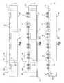
- FIGS. 1A-Fare schematic cross-sectional views illustrating stages of a method for manufacturing semiconductor components in accordance with an embodiment of the invention.
- FIG. 2is a schematic cross-sectional view of a semiconductor component in accordance with an embodiment of the invention.
- FIG. 3is a flow chart of a method for fabricating semiconductor components in accordance with an embodiment of the invention.
- FIG. 4is a flow chart of a method for fabricating semiconductor components in accordance with another embodiment of the invention.
- FIG. 5is a flow chart of a method for fabricating semiconductor components in accordance with another embodiment of the invention.
- FIG. 6is a schematic cross-sectional view of a portion of a semiconductor wafer at a stage of a method for fabricating semiconductor components in accordance with an embodiment of the invention.
- FIG. 7is a schematic view of a system that incorporates semiconductor components in accordance with embodiments of the invention.
- the semiconductor componentsare manufactured on semiconductor wafers that can include substrates upon which and/or in which microelectronic devices, micromechanical devices, data storage elements, optics, read/write components, and other features are fabricated.
- SRAMstatic random access memory
- DRAMdynamic random access memory
- flash memorye.g., NAND flash-memory
- processorsimagers, and other types of devices can be constructed on semiconductor wafers.
- FIG. 1Aillustrates a semiconductor wafer 10 at one stage of an embodiment of a method for fabricating semiconductor components.
- the wafer 10includes a substrate 12 having a first side 14 , a back surface 16 , and a plurality of die contacts 18 or other types of electrical input/output terminals at the first side 14 .
- the first side 14is accordingly an active side or circuit side of the wafer 10 .
- the wafer 10further includes a plurality of dies 20 , and individual dies include an integrated circuit 26 electrically coupled to corresponding die contacts 18 at the first side 14 .
- the dies 20can comprise any type of semiconductor device having a desired configuration.
- each die 20can comprise a dynamic random access memory (DRAM), a static random access memory (SRAM), a flash memory, a micro-processor, a digital signal processor, an application specific integrated circuit, an imager, or other type of semiconductor device.
- the wafer 10further includes a plurality of lanes 30 between the dies 20 .
- the dies 20are typically arranged in a grid or other type of pattern on the wafer 10 according to the specific application.
- FIG. 1Aprovides one example of a semiconductor wafer in which the die contacts 18 are located at the first side 14 of the wafer 10 .
- the die contacts 18can be located on the back surface 16 or at a second surface of the substrate formed later by thinning the wafer 10 .
- the die contacts 18are connected to the integrated circuits 26 using interconnects that pass to the backside of the wafer.
- the following processesare described as being performed on the first side 14 and then the back surface 16 , it is to be understood that any of the operations can be reversed.
- the illustrated die contacts 18are arranged in two rows along the center of each die 20 , the die contacts 18 can be in arrays that have different configurations.
- the die contacts 18are generally circular-shaped metal pads having a desired size and spacing.
- the die contacts 18can comprise nickel, copper, gold, silver, platinum, palladium, tin, zinc, alloys of these metals, and/or other metals suitable for soldering.
- FIG. 1Billustrates the wafer 10 at a stage in which contact bumps 24 or other connectors are formed on the die contacts 18 .
- the contact bumps 24can comprise metal bumps deposited on the die contacts 18 using a suitable deposition process, such as stenciling/reflow, ball deposits, and other processes.
- the contact bumps 24can comprise solder, gold balls, other metals, or a conductive polymer.
- the contact bumps 24are used to interconnect the die contacts 18 to corresponding terminals on a printed circuit board, lead frame, module, or other suitable device.
- a dicing tape 32can be attached to the back surface 16 of the wafer 10 .
- FIG. 1Cillustrates the wafer 10 at a subsequent stage of the method in which a plurality of first trenches 40 are formed along the lanes 30 at the first side 14 of the wafer 10 .
- the first trenches 40are arranged in a grid between the dies 20 .
- the first trenches 40can be formed by scribing the wafer along the lanes 30 using a dicing saw having blades set such that the kerfs extend to only an intermediate depth d 1 within the wafer 10 .
- the first trenches 40can alternatively be formed using an etching process that etches the first trenches 40 through an etch mask (not shown) formed on the first side 14 of the wafer 10 .
- the etching processcan be a wet etching process, a dry etching process, or a plasma etching process.
- the depth d 1 of the first trenches 40can be controlled using suitable endpointing techniques.
- Another alternative for forming the first trenches 40is laser machining the wafer 10 . Suitable laser systems for forming the first trenches 40 are manufactured by Electro Scientific, Inc., of Portland, Oreg. (e.g., Model Number 2700).
- the first trenches 40do not extend through the full thickness Tw 1 of the wafer 10 defined by the distance between the first side 14 and the back surface 16 . Rather, the first trenches 40 have an intermediate depth d 1 measured from the surface of the first side 14 of the wafer 10 that is less than the thickness Tw 1 .
- the initial thickness Tw 1 of the wafer 10is approximately 700-1,000 microns (e.g., approximately 750 microns), and the first trenches 40 have a depth d 1 of less than approximately 250 microns.
- the depth d 1 of the first trenches 40for example, can be approximately 50-200 microns. As explained more fully below, the depth d 1 is also less than a final wafer thickness of the wafer 10 after it has been thinned.
- FIG. 1Dillustrates a subsequent stage in the method in which the first trenches 40 are filled with a first protective material 50 .
- the first protective material 50can form a first cover member having a front side portion 52 covering the first side 14 and first extensions 54 in the first trenches 40 .
- the first cover membercan be formed by depositing a polymeric material onto the first side 14 of the wafer 10 using suitable molding techniques, screen printing, stenciling, or spin-on processes.
- the first protective material 50can comprise a curable polymer, such as a silicone, a polyimide, or an epoxy.
- the first protective material 50can include fillers, such as silicates, or other materials that reduce the coefficient of thermal expansion and control the viscosity of the first protective material 50 .
- the first protective material 50can be cured at this stage to harden the material.
- curingcan be formed by placing the wafer 10 in a chamber having a temperature of about 90 degrees to 165 degrees C. for about 30-60 minutes. In other embodiments, however, the first protective material 50 can be cured at a later stage of the method.
- FIG. 1Eillustrates the wafer 10 at a subsequent stage of the method in which the wafer 10 has been thinned to form a second side 17 opposite the first side 14 .
- the wafer 10can be thinned by grinding the wafer 10 from the back surface 16 ( FIG. 1D ) at the first thickness Tw 1 to the second side 17 at a second thickness Tw 2 .
- the second thickness Tw 2can be approximately 300-500 microns (e.g., approximately 450 microns). In other embodiments, the second thickness can be more or less than 300-500 microns.
- a plurality of second trenches 60are formed in the second side 17 along the lanes 30 .
- the second trenches 60are at least generally aligned with the first trenches 40 at the first side 14 of the wafer 10 , and the second trenches 60 have a second intermediate depth d 2 from the second side 17 that does not extend to the intermediate depth d 1 of the first trenches 40 .
- the widths and depths of the first and second trenches 40 and 60are the same.
- the second trenches 60are separated from the first trenches 40 by shoulders 19 in the lanes 30 . The shoulders 19 are portions of the wafer 10 .
- the second trenches 60can be formed by sawing, etching, or laser cutting, as described above with respect to the first trenches 40 in FIG. 1C .
- FIG. 1Fillustrates the wafer 10 at another stage of the method in which a second protective material 70 is deposited onto the second side 17 of the wafer 10 .
- the second protective material 70fills at least a portion of the second trenches 60 .
- the second protective material 70can be the same as the first protective material 50 , or the second protective material 70 can be different than the first protective material 50 .
- the second protective material 70can be a polymeric material, such as a silicone, a polyimide, or an epoxy, either with or without suitable fillers.
- the second protective material 70can be molded to form a second cover member having a backside portion 72 that covers the second side 17 and second extensions 74 in the second trenches 60 .
- the second protective material 70can be cured to harden the second cover member.
- the first protective material 50 and the second protective material 70can be cured at the same time after depositing the second protective material 70 onto the second side 17 of the wafer 10 .
- the wafer 10can be cut along the lanes 30 between the dies 20 to separate the dies 20 from each other.
- the wafer 10is cut such that the kerf k of the cut is less than the width w of the first and second trenches 40 and 60 .
- the first and second trenches 40 and 60should be aligned and the kerfs k should be centered in the trenches so that the thickness of the protective materials around the sidewall of the dies 20 is consistent.
- FIG. 2is a schematic cross-sectional view illustrating a semiconductor component 100 formed from a portion of the wafer 10 ( FIG. 1 ) after cutting the wafer 10 along the lanes 30 .
- the semiconductor component 100includes a die 20 , a first exterior cover 51 of the first protective material 50 formed from the first cover member, and a second exterior cover 71 of the second protective material 70 formed from the second cover member.
- the die 20has a sidewall with a first indentation 21 a around the periphery of the die 20 at the first side 14 , a second indentation 21 b around the periphery of the die 20 at the second side 17 , and the shoulder 19 projecting outwardly around the periphery of the die 20 .
- the first exterior cover 51accordingly has the front side portion 52 over the first side 14 and the first extension 54 projecting from the front side portion 52 in the first indentation 21 a .
- the second exterior cover 71has a backside portion 72 over the second side 17 and the second extension 74 projecting from the backside portion 72 in the second indentation 21 b .
- the first protective cover 51 and the second protective cover 71encase virtually all of the die 20 except for an exposed portion 23 of the shoulder 19 between the first extension 54 and the second extension 74 .
- the semiconductor component 100has pseudo six-sided protection except for the exposed portion 23 of the shoulder 19 .
- the front side portion 52 of the first exterior cover 51has a thickness T 1 and the first extension 54 has a thickness of T 2 at least substantially equal to the thickness T 1 . Accordingly, the forces exerted by the first exterior cover 51 on the die 20 during thermal cycling are equal for both the front side portion 52 and the first extension 54 .
- the backside portion 72 of the second exterior cover 71has a thickness T 3 and the second extension 74 has a thickness T 4 substantially equal to the thickness T 3 Moreover, in a specific embodiment, the thicknesses T 1 , T 2 , T 3 , and T 4 can all be substantially equal to each other such that the forces exerted on the die 20 by the first exterior cover 51 are substantially equal to the forces exerted on the die 20 by the second exterior cover 71 . Such equal loading on the front side and backside of the die 20 can reduce flexing and warpage of the die 20 .
- the semiconductor component 100can provide the virtual equivalent of complete six-sided protection for the die 20 with a thicker substrate than existing six-sided packages formed using trenches cut in only one side of the wafer. More specifically, it is difficult to cut trenches deeper than approximately 250 microns in the wafer, and thus the dies in many existing six-sided packages are thinned to less than approximately 250 microns before applying the polymeric material to the backside of the dies. Such thin dies are subject to warping or breaking during subsequent handling and/or thermal cycling.
- the semiconductor component 100can have a thickness substantially greater than 250 microns (e.g., 300-700 microns) because the first and second trenches are aligned with each other and spaced apart by a portion of the wafer (e.g., the shoulders).
- the semiconductor component 100provides a robust device with the virtual equivalent of complete six-sided encapsulation.
- the semiconductor component 100can be packaged at the wafer level without having to handle individual dies before they are fully protected. This may reduce the damage caused by handling unprotected dies before they are encapsulated that may occur in many existing packaging processes. More specifically, by performing a partial scribe from each side of the wafer, the motion of the wafer is constrained while still allowing formation of full front side and backside encapsulation for protection of the exposed corners of the die 20 . The full corner protection shown in the illustrated embodiment of the semiconductor component 100 can survive the environmental testing and operation conditions while preventing edge separation.
- Specific embodiments of the semiconductor component 100can further provide uniform loading on the wafer. For example, by forming the first exterior cover and the second exterior cover to have approximately equal thicknesses, the stresses induced by thermal contraction/expansion of the first and second exterior covers can be approximately equal. In these embodiments, the loading on the front side counteracts the loading on the backside to mitigate or eliminate warpage and cracking.
- FIG. 3is a flow chart of an embodiment of a method 300 for manufacturing semiconductor components.
- the method 300includes forming a plurality of first trenches in lanes between dies on a first side of a semiconductor wafer (block 310 ), and filling at least a portion of the first trenches with a protective material (block 320 ).
- the method 300continues by forming a plurality of second trenches on a second side of the wafer that are at least generally aligned with the first trenches along the cutting lanes (block 330 ). As explained above, many applications should have good alignment between the first and second trenches, but a certain degree of misalignment can be acceptable.
- the method 300further includes filling at least a portion of the second trenches with the protective material (block 340 ), and cutting through the wafer along the lanes (block 350 ). The semiconductor components are thus formed after cutting through the wafer along the cutting lanes.
- FIG. 4illustrates an embodiment of another method 400 for manufacturing semiconductor components.
- the method 400includes depositing a protective material on a first side of a semiconductor wafer having a plurality of dies so that the protective material is in first trenches between the dies on the first side of the wafer (block 410 ).
- the method 400also includes depositing a protective material on a second side of the wafer so that the protective material is in second trenches on the second side of the wafer (block 420 ).
- the second trenchesare at least generally aligned with the first trenches.
- the protective material in the first trenchescan be the same as the protective material in the second trenches. In alternative embodiments, however, the protective material in the second trenches is different than that in the first trenches.
- the method 400further includes separating the wafer along the first and second trenches (block 430 ).
- FIG. 5is a flow chart illustrating an embodiment of still another method 500 for manufacturing semiconductor components.
- the method 500includes mounting conductive balls or bumps to die contacts connected to integrated circuits of dies on a semiconductor wafer (block 510 ).
- the die contactsare at a first side of the wafer.
- the method 500continues by cutting first trenches into the first side of the wafer along lanes adjacent to the dies such that the first trenches have a first depth in the wafer (block 520 ).
- the method 500further includes molding a polymeric material onto the first side and into the first trenches (block 530 ) and thinning the wafer to a second side opposite the first side (block 540 ).
- the method 500also includes cutting second trenches into the second side of the wafer after the thinning procedure so that the second trenches are at least generally aligned with the first trenches along the lanes (block 550 ) and molding the polymeric material onto the second side and into the second trenches (block 560 ).
- the method 500further includes cutting the wafer along the dicing lanes (block 570 ).
- the process of cutting the waferforms individual packaged components that have a first exterior cover at the first side with a first extension extending toward the second side, a second exterior cover at the second side with a second extension extending toward the first side, and a sidewall between the first and second sides.
- the sidewallincludes an exterior portion of the first extension, an exterior portion of the second extension, and an exposed portion of the semiconductor wafer between the first and second extensions.
- FIG. 6is a cross-sectional view illustrating semiconductor components 600 in accordance with another embodiment.
- the semiconductor components 600are similar to the semiconductor component 100 illustrated in FIG. 2 , but the semiconductor components 600 have first and second channels or trenches 640 and 660 , respectively, that have slanted or inclined sidewalls along first and second indentations 621 a and 621 b , respectively.
- the inclined portions of the first and second indentations 621 a and 621 bcan be formed using a beveled saw to cut the first and second channels 640 and 660 , respectively.
- each semiconductor component 600has a first exterior cover 51 with a first beveled extension 654 and a second exterior cover 71 with a second beveled extension 674 .
- any one of the semiconductor components described above with reference to FIGS. 1A-6can be incorporated into any of a myriad of larger and/or more complex systems, a representative example of which is system 700 shown schematically in FIG. 7 .
- the system 700can include a processor 701 , a memory 702 (e.g., SRAM, DRAM, flash, and/or other memory device), input/output devices 703 , and/or other subsystems or components 704 .
- the foregoing semiconductor components described above with reference to FIGS. 1A-6may be included in any of the components shown in FIG. 7 .
- the resulting system 700can perform any of a wide variety of computing, processing, storage, sensing, imaging, and/or other functions.
- representative systems 700include, without limitation, computers and/or other data processors, for example, desktop computers, laptop computers, Internet appliances, hand-held devices (e.g., palm-top computers, wearable computers, cellular or mobile phones, personal digital assistants, etc.), multi-processor systems, processor-based or programmable consumer electronics, network computers, and minicomputers.
- Other representative systems 700include cameras, light or other radiation sensors, servers and associated server subsystems, display devices, and/or other memory devices.
- individual diescan include imager arrays, such as CMOS imagers.
- Components of the system 700may be housed in a single unit or distributed over multiple, interconnected units (e.g., through a communications network).
- the components of the system 700can accordingly include local and/or remote memory storage devices, and any of a wide variety of computer readable media.
- solder ballscan be deposited onto the first side of the wafer after forming the first trenches.
- the second trenchescan be formed from the back surface 16 ( FIG. 1D ) before thinning the wafer to form the second side 17 ( FIG. 1E ).
- singular or plural termsmay also include plural or singular terms, respectively.
Landscapes
- Engineering & Computer Science (AREA)
- Physics & Mathematics (AREA)
- Condensed Matter Physics & Semiconductors (AREA)
- General Physics & Mathematics (AREA)
- Computer Hardware Design (AREA)
- Microelectronics & Electronic Packaging (AREA)
- Power Engineering (AREA)
- Manufacturing & Machinery (AREA)
- Dicing (AREA)
- Structures Or Materials For Encapsulating Or Coating Semiconductor Devices Or Solid State Devices (AREA)
Abstract
Description
Claims (24)
Priority Applications (4)
| Application Number | Priority Date | Filing Date | Title |
|---|---|---|---|
| US11/681,648US7833881B2 (en) | 2007-03-02 | 2007-03-02 | Methods for fabricating semiconductor components and packaged semiconductor components |
| PCT/US2008/055528WO2008109457A1 (en) | 2007-03-02 | 2008-02-29 | Methods for fabricating packaged semiconductor components |
| TW097107415ATW200901339A (en) | 2007-03-02 | 2008-03-03 | Methods for fabricating semiconductor components and packaged semiconductor components |
| US12/906,818US20110031614A1 (en) | 2007-03-02 | 2010-10-18 | Methods for fabricating semiconductor components and packaged semiconductor components |
Applications Claiming Priority (1)
| Application Number | Priority Date | Filing Date | Title |
|---|---|---|---|
| US11/681,648US7833881B2 (en) | 2007-03-02 | 2007-03-02 | Methods for fabricating semiconductor components and packaged semiconductor components |
Related Child Applications (1)
| Application Number | Title | Priority Date | Filing Date |
|---|---|---|---|
| US12/906,818DivisionUS20110031614A1 (en) | 2007-03-02 | 2010-10-18 | Methods for fabricating semiconductor components and packaged semiconductor components |
Publications (2)
| Publication Number | Publication Date |
|---|---|
| US20080213976A1 US20080213976A1 (en) | 2008-09-04 |
| US7833881B2true US7833881B2 (en) | 2010-11-16 |
Family
ID=39598429
Family Applications (2)
| Application Number | Title | Priority Date | Filing Date |
|---|---|---|---|
| US11/681,648Active2028-09-23US7833881B2 (en) | 2007-03-02 | 2007-03-02 | Methods for fabricating semiconductor components and packaged semiconductor components |
| US12/906,818AbandonedUS20110031614A1 (en) | 2007-03-02 | 2010-10-18 | Methods for fabricating semiconductor components and packaged semiconductor components |
Family Applications After (1)
| Application Number | Title | Priority Date | Filing Date |
|---|---|---|---|
| US12/906,818AbandonedUS20110031614A1 (en) | 2007-03-02 | 2010-10-18 | Methods for fabricating semiconductor components and packaged semiconductor components |
Country Status (3)
| Country | Link |
|---|---|
| US (2) | US7833881B2 (en) |
| TW (1) | TW200901339A (en) |
| WO (1) | WO2008109457A1 (en) |
Cited By (7)
| Publication number | Priority date | Publication date | Assignee | Title |
|---|---|---|---|---|
| US20090072375A1 (en)* | 2007-09-18 | 2009-03-19 | Sungmin Song | Integrated circuit package system with multi-chip module |
| US20090174023A1 (en)* | 2007-12-28 | 2009-07-09 | Hidekazu Takahashi | Semiconductor device and method of manufacturing semiconductor device |
| US20090183766A1 (en)* | 2008-01-22 | 2009-07-23 | Hidekazu Takahashi | Semiconductor device and method of manufacturing semiconductor device |
| US20090194154A1 (en)* | 2008-02-01 | 2009-08-06 | Semiconductor Energy Laboratory Co., Ltd. | Semiconductor device and method of manufacturing semiconductor device |
| US20140346642A1 (en)* | 2011-09-06 | 2014-11-27 | Vishay Semiconductor Gmbh | Surface mountable electronic component |
| US10283466B2 (en)* | 2016-05-31 | 2019-05-07 | Semiconductor Components Industries, Llc | Polymer resin and compression mold chip scale package |
| US12057357B2 (en) | 2020-08-12 | 2024-08-06 | Samsung Electronics Co, Ltd. | Semiconductor package including plurality of recesses and molding member with plurality of protrusions that fill the recesses |
Families Citing this family (20)
| Publication number | Priority date | Publication date | Assignee | Title |
|---|---|---|---|---|
| US7833881B2 (en)* | 2007-03-02 | 2010-11-16 | Micron Technology, Inc. | Methods for fabricating semiconductor components and packaged semiconductor components |
| TWI364793B (en)* | 2007-05-08 | 2012-05-21 | Mutual Pak Technology Co Ltd | Package structure for integrated circuit device and method of the same |
| US8298917B2 (en)* | 2009-04-14 | 2012-10-30 | International Business Machines Corporation | Process for wet singulation using a dicing singulation structure |
| US20110039397A1 (en)* | 2009-08-17 | 2011-02-17 | Huilong Zhu | Structures and methods to separate microchips from a wafer |
| US8446007B2 (en) | 2009-10-20 | 2013-05-21 | Taiwan Semiconductor Manufacturing Company, Ltd. | Non-uniform alignment of wafer bumps with substrate solders |
| US8987878B2 (en) | 2010-10-29 | 2015-03-24 | Alpha And Omega Semiconductor Incorporated | Substrateless power device packages |
| KR101712630B1 (en) | 2010-12-20 | 2017-03-07 | 삼성전자 주식회사 | Method for forming semiconductor device |
| JP5659033B2 (en)* | 2011-02-04 | 2015-01-28 | 株式会社東芝 | Manufacturing method of semiconductor device |
| US9196532B2 (en) | 2012-06-21 | 2015-11-24 | Taiwan Semiconductor Manufacturing Company, Ltd. | Integrated circuit packages and methods for forming the same |
| JP6078272B2 (en)* | 2012-09-10 | 2017-02-08 | 株式会社ディスコ | Wafer processing method |
| US9000587B1 (en)* | 2013-03-12 | 2015-04-07 | Maxim Integrated Products, Inc. | Wafer-level thin chip integration |
| US9698070B2 (en)* | 2013-04-11 | 2017-07-04 | Infineon Technologies Ag | Arrangement having a plurality of chips and a chip carrier, and a processing arrangement |
| US9165831B2 (en)* | 2013-06-27 | 2015-10-20 | Globalfoundries Inc. | Dice before grind with backside metal |
| US9484308B2 (en)* | 2014-06-25 | 2016-11-01 | Taiwan Semiconductor Manufacturing Company Ltd. | Semiconductor device |
| US9514925B1 (en)* | 2015-09-10 | 2016-12-06 | Amazon Technologies, Inc. | Protective coating for silicon substrate |
| US10319639B2 (en)* | 2017-08-17 | 2019-06-11 | Semiconductor Components Industries, Llc | Thin semiconductor package and related methods |
| US20170256432A1 (en)* | 2016-03-03 | 2017-09-07 | Nexperia B.V. | Overmolded chip scale package |
| US10410922B2 (en) | 2017-02-23 | 2019-09-10 | Nxp B.V. | Semiconductor device with six-sided protected walls |
| US11508692B2 (en)* | 2019-12-25 | 2022-11-22 | Taiwan Semiconductor Manufacturing Company, Ltd. | Package structure and method of fabricating the same |
| WO2021132678A1 (en)* | 2019-12-27 | 2021-07-01 | リンテック株式会社 | Semiconductor chip production method |
Citations (10)
| Publication number | Priority date | Publication date | Assignee | Title |
|---|---|---|---|---|
| JPH11162885A (en) | 1997-11-26 | 1999-06-18 | Sharp Corp | Method for manufacturing semiconductor device |
| JPH11177139A (en) | 1997-12-16 | 1999-07-02 | Nichia Chem Ind Ltd | Semiconductor light emitting device and method of manufacturing the same |
| US6326698B1 (en)* | 2000-06-08 | 2001-12-04 | Micron Technology, Inc. | Semiconductor devices having protective layers thereon through which contact pads are exposed and stereolithographic methods of fabricating such semiconductor devices |
| US6338980B1 (en) | 1999-08-13 | 2002-01-15 | Citizen Watch Co., Ltd. | Method for manufacturing chip-scale package and manufacturing IC chip |
| US6579748B1 (en) | 1999-05-18 | 2003-06-17 | Sanyu Rec Co., Ltd. | Fabrication method of an electronic component |
| US20040051118A1 (en) | 2002-07-19 | 2004-03-18 | Bruhns Michael T. | Trench cut light emitting diodes and methods of fabricating same |
| US20040113283A1 (en) | 2002-03-06 | 2004-06-17 | Farnworth Warren M. | Method for fabricating encapsulated semiconductor components by etching |
| US20050250234A1 (en)* | 2004-05-10 | 2005-11-10 | Sharp Kabushiki Kaisha | Semiconductor device and method for fabrication thereof |
| US20060189029A1 (en)* | 2005-02-24 | 2006-08-24 | Koduri Sreenivasan K | Method for efficient annealing of plated semiconductor package leads |
| US20070029684A1 (en) | 2005-08-02 | 2007-02-08 | Disco Corporation | Wafer dividing method |
Family Cites Families (3)
| Publication number | Priority date | Publication date | Assignee | Title |
|---|---|---|---|---|
| JP3497722B2 (en)* | 1998-02-27 | 2004-02-16 | 富士通株式会社 | Semiconductor device, method of manufacturing the same, and transfer tray thereof |
| US7001827B2 (en)* | 2003-04-15 | 2006-02-21 | International Business Machines Corporation | Semiconductor wafer front side protection |
| US7833881B2 (en)* | 2007-03-02 | 2010-11-16 | Micron Technology, Inc. | Methods for fabricating semiconductor components and packaged semiconductor components |
- 2007
- 2007-03-02USUS11/681,648patent/US7833881B2/enactiveActive
- 2008
- 2008-02-29WOPCT/US2008/055528patent/WO2008109457A1/enactiveApplication Filing
- 2008-03-03TWTW097107415Apatent/TW200901339A/enunknown
- 2010
- 2010-10-18USUS12/906,818patent/US20110031614A1/ennot_activeAbandoned
Patent Citations (18)
| Publication number | Priority date | Publication date | Assignee | Title |
|---|---|---|---|---|
| JPH11162885A (en) | 1997-11-26 | 1999-06-18 | Sharp Corp | Method for manufacturing semiconductor device |
| JPH11177139A (en) | 1997-12-16 | 1999-07-02 | Nichia Chem Ind Ltd | Semiconductor light emitting device and method of manufacturing the same |
| US6579748B1 (en) | 1999-05-18 | 2003-06-17 | Sanyu Rec Co., Ltd. | Fabrication method of an electronic component |
| US6338980B1 (en) | 1999-08-13 | 2002-01-15 | Citizen Watch Co., Ltd. | Method for manufacturing chip-scale package and manufacturing IC chip |
| US6326698B1 (en)* | 2000-06-08 | 2001-12-04 | Micron Technology, Inc. | Semiconductor devices having protective layers thereon through which contact pads are exposed and stereolithographic methods of fabricating such semiconductor devices |
| US20050181540A1 (en) | 2002-03-06 | 2005-08-18 | Farnworth Warren M. | Semiconductor component and system having thinned, encapsulated dice |
| US20040113283A1 (en) | 2002-03-06 | 2004-06-17 | Farnworth Warren M. | Method for fabricating encapsulated semiconductor components by etching |
| US20050148160A1 (en) | 2002-03-06 | 2005-07-07 | Farnworth Warren M. | Encapsulated semiconductor components and methods of fabrication |
| US20050200028A1 (en) | 2002-03-06 | 2005-09-15 | Farnworth Warren M. | Encapsulated semiconductor component having thinned die with conductive vias |
| US20050227415A1 (en)* | 2002-03-06 | 2005-10-13 | Farnworth Warren M | Method for fabricating encapsulated semiconductor components |
| US6964915B2 (en) | 2002-03-06 | 2005-11-15 | Micron Technology, Inc. | Method of fabricating encapsulated semiconductor components by etching |
| US20050269700A1 (en) | 2002-03-06 | 2005-12-08 | Farnworth Warren M | Semiconductor component and system having thinned, encapsulated dice |
| US7029949B2 (en) | 2002-03-06 | 2006-04-18 | Micron Technology, Inc. | Method for fabricating encapsulated semiconductor components having conductive vias |
| US20060183349A1 (en) | 2002-03-06 | 2006-08-17 | Farnworth Warren M | Semiconductor component having thinned die with polymer layers |
| US20040051118A1 (en) | 2002-07-19 | 2004-03-18 | Bruhns Michael T. | Trench cut light emitting diodes and methods of fabricating same |
| US20050250234A1 (en)* | 2004-05-10 | 2005-11-10 | Sharp Kabushiki Kaisha | Semiconductor device and method for fabrication thereof |
| US20060189029A1 (en)* | 2005-02-24 | 2006-08-24 | Koduri Sreenivasan K | Method for efficient annealing of plated semiconductor package leads |
| US20070029684A1 (en) | 2005-08-02 | 2007-02-08 | Disco Corporation | Wafer dividing method |
Non-Patent Citations (1)
| Title |
|---|
| International Search Report and Written Opinion for PCT/US2008/055528, Aug. 1, 2008. |
Cited By (15)
| Publication number | Priority date | Publication date | Assignee | Title |
|---|---|---|---|---|
| US20090072375A1 (en)* | 2007-09-18 | 2009-03-19 | Sungmin Song | Integrated circuit package system with multi-chip module |
| US9330945B2 (en)* | 2007-09-18 | 2016-05-03 | Stats Chippac Ltd. | Integrated circuit package system with multi-chip module |
| US20090174023A1 (en)* | 2007-12-28 | 2009-07-09 | Hidekazu Takahashi | Semiconductor device and method of manufacturing semiconductor device |
| US8999818B2 (en)* | 2007-12-28 | 2015-04-07 | Semiconductor Energy Laboratory Co., Ltd. | Semiconductor device and method of manufacturing semiconductor device |
| US8610152B2 (en) | 2008-01-22 | 2013-12-17 | Semiconductor Energy Laboratory Co., Ltd. | Semiconductor device and method of manufacturing semiconductor device |
| US8324079B2 (en) | 2008-01-22 | 2012-12-04 | Semiconductor Energy Laboratory Co., Ltd. | Method of manufacturing semiconductor device |
| US20090183766A1 (en)* | 2008-01-22 | 2009-07-23 | Hidekazu Takahashi | Semiconductor device and method of manufacturing semiconductor device |
| US8227886B2 (en) | 2008-02-01 | 2012-07-24 | Semiconductor Energy Laboratory Co., Ltd. | Semiconductor device and method of manufacturing semiconductor device |
| US20090194154A1 (en)* | 2008-02-01 | 2009-08-06 | Semiconductor Energy Laboratory Co., Ltd. | Semiconductor device and method of manufacturing semiconductor device |
| US20140346642A1 (en)* | 2011-09-06 | 2014-11-27 | Vishay Semiconductor Gmbh | Surface mountable electronic component |
| US10629485B2 (en)* | 2011-09-06 | 2020-04-21 | Vishay Semiconductor Gmbh | Surface mountable electronic component |
| US10283466B2 (en)* | 2016-05-31 | 2019-05-07 | Semiconductor Components Industries, Llc | Polymer resin and compression mold chip scale package |
| US10825786B2 (en) | 2016-05-31 | 2020-11-03 | Semiconductor Components Industries, Llc | Polymer resin and compression mold chip scale package |
| US11508679B2 (en) | 2016-05-31 | 2022-11-22 | Semiconductor Components Industries, Llc | Polymer resin and compression mold chip scale package |
| US12057357B2 (en) | 2020-08-12 | 2024-08-06 | Samsung Electronics Co, Ltd. | Semiconductor package including plurality of recesses and molding member with plurality of protrusions that fill the recesses |
Also Published As
| Publication number | Publication date |
|---|---|
| TW200901339A (en) | 2009-01-01 |
| WO2008109457A1 (en) | 2008-09-12 |
| US20110031614A1 (en) | 2011-02-10 |
| US20080213976A1 (en) | 2008-09-04 |
Similar Documents
| Publication | Publication Date | Title |
|---|---|---|
| US7833881B2 (en) | Methods for fabricating semiconductor components and packaged semiconductor components | |
| US20220122938A1 (en) | Packaged microelectronic devices having stacked interconnect elements and methods for manufacturing the same | |
| KR101186712B1 (en) | Microfeature workpieces having interconnects and conductive backplanes, and associated systems and methods | |
| US8138021B2 (en) | Apparatus for packaging semiconductor devices, packaged semiconductor components, methods of manufacturing apparatus for packaging semiconductor devices, and methods of manufacturing semiconductor components | |
| TWI500091B (en) | Method of packaging a semiconductor device and packaging device | |
| US7947529B2 (en) | Microelectronic die packages with leadframes, including leadframe-based interposer for stacked die packages, and associated systems and methods | |
| US9177919B2 (en) | Chip package and method for forming the same | |
| US7939916B2 (en) | Wafer level CSP packaging concept | |
| US7928582B2 (en) | Microelectronic workpieces and methods for manufacturing microelectronic devices using such workpieces | |
| US9611143B2 (en) | Method for forming chip package | |
| US10163662B2 (en) | Fabrication method of semiconductor package | |
| US10825782B2 (en) | Semiconductor packages and associated methods with solder mask opening(s) for in-package ground and conformal coating contact | |
| CN105047629A (en) | Image sensing element packaging component and manufacturing method thereof | |
| US10867947B2 (en) | Semiconductor packages and methods of manufacturing the same | |
| KR20140123695A (en) | Semiconductor package using glass and method for manufacturing the same | |
| US9431334B2 (en) | Semiconductor device having single layer substrate and method | |
| JP3291289B2 (en) | Electronic component manufacturing method | |
| US20160141217A1 (en) | Electronic package and fabrication method thereof | |
| KR20080025876A (en) | Semiconductor device protective structure and method for manufacturing same |
Legal Events
| Date | Code | Title | Description |
|---|---|---|---|
| AS | Assignment | Owner name:MICRON TECHNOLOGY, INC., IDAHO Free format text:ASSIGNMENT OF ASSIGNORS INTEREST;ASSIGNOR:FARNWORTH, WARREN M.;REEL/FRAME:018954/0984 Effective date:20070227 | |
| FEPP | Fee payment procedure | Free format text:PAYOR NUMBER ASSIGNED (ORIGINAL EVENT CODE: ASPN); ENTITY STATUS OF PATENT OWNER: LARGE ENTITY | |
| STCF | Information on status: patent grant | Free format text:PATENTED CASE | |
| FPAY | Fee payment | Year of fee payment:4 | |
| AS | Assignment | Owner name:U.S. BANK NATIONAL ASSOCIATION, AS COLLATERAL AGENT, CALIFORNIA Free format text:SECURITY INTEREST;ASSIGNOR:MICRON TECHNOLOGY, INC.;REEL/FRAME:038669/0001 Effective date:20160426 Owner name:U.S. BANK NATIONAL ASSOCIATION, AS COLLATERAL AGEN Free format text:SECURITY INTEREST;ASSIGNOR:MICRON TECHNOLOGY, INC.;REEL/FRAME:038669/0001 Effective date:20160426 | |
| AS | Assignment | Owner name:MORGAN STANLEY SENIOR FUNDING, INC., AS COLLATERAL AGENT, MARYLAND Free format text:PATENT SECURITY AGREEMENT;ASSIGNOR:MICRON TECHNOLOGY, INC.;REEL/FRAME:038954/0001 Effective date:20160426 Owner name:MORGAN STANLEY SENIOR FUNDING, INC., AS COLLATERAL Free format text:PATENT SECURITY AGREEMENT;ASSIGNOR:MICRON TECHNOLOGY, INC.;REEL/FRAME:038954/0001 Effective date:20160426 | |
| AS | Assignment | Owner name:U.S. BANK NATIONAL ASSOCIATION, AS COLLATERAL AGENT, CALIFORNIA Free format text:CORRECTIVE ASSIGNMENT TO CORRECT THE REPLACE ERRONEOUSLY FILED PATENT #7358718 WITH THE CORRECT PATENT #7358178 PREVIOUSLY RECORDED ON REEL 038669 FRAME 0001. ASSIGNOR(S) HEREBY CONFIRMS THE SECURITY INTEREST;ASSIGNOR:MICRON TECHNOLOGY, INC.;REEL/FRAME:043079/0001 Effective date:20160426 Owner name:U.S. BANK NATIONAL ASSOCIATION, AS COLLATERAL AGEN Free format text:CORRECTIVE ASSIGNMENT TO CORRECT THE REPLACE ERRONEOUSLY FILED PATENT #7358718 WITH THE CORRECT PATENT #7358178 PREVIOUSLY RECORDED ON REEL 038669 FRAME 0001. ASSIGNOR(S) HEREBY CONFIRMS THE SECURITY INTEREST;ASSIGNOR:MICRON TECHNOLOGY, INC.;REEL/FRAME:043079/0001 Effective date:20160426 | |
| MAFP | Maintenance fee payment | Free format text:PAYMENT OF MAINTENANCE FEE, 8TH YEAR, LARGE ENTITY (ORIGINAL EVENT CODE: M1552) Year of fee payment:8 | |
| AS | Assignment | Owner name:JPMORGAN CHASE BANK, N.A., AS COLLATERAL AGENT, ILLINOIS Free format text:SECURITY INTEREST;ASSIGNORS:MICRON TECHNOLOGY, INC.;MICRON SEMICONDUCTOR PRODUCTS, INC.;REEL/FRAME:047540/0001 Effective date:20180703 Owner name:JPMORGAN CHASE BANK, N.A., AS COLLATERAL AGENT, IL Free format text:SECURITY INTEREST;ASSIGNORS:MICRON TECHNOLOGY, INC.;MICRON SEMICONDUCTOR PRODUCTS, INC.;REEL/FRAME:047540/0001 Effective date:20180703 | |
| AS | Assignment | Owner name:MICRON TECHNOLOGY, INC., IDAHO Free format text:RELEASE BY SECURED PARTY;ASSIGNOR:U.S. BANK NATIONAL ASSOCIATION, AS COLLATERAL AGENT;REEL/FRAME:047243/0001 Effective date:20180629 | |
| AS | Assignment | Owner name:MICRON TECHNOLOGY, INC., IDAHO Free format text:RELEASE BY SECURED PARTY;ASSIGNOR:MORGAN STANLEY SENIOR FUNDING, INC., AS COLLATERAL AGENT;REEL/FRAME:050937/0001 Effective date:20190731 | |
| AS | Assignment | Owner name:MICRON TECHNOLOGY, INC., IDAHO Free format text:RELEASE BY SECURED PARTY;ASSIGNOR:JPMORGAN CHASE BANK, N.A., AS COLLATERAL AGENT;REEL/FRAME:051028/0001 Effective date:20190731 Owner name:MICRON SEMICONDUCTOR PRODUCTS, INC., IDAHO Free format text:RELEASE BY SECURED PARTY;ASSIGNOR:JPMORGAN CHASE BANK, N.A., AS COLLATERAL AGENT;REEL/FRAME:051028/0001 Effective date:20190731 | |
| MAFP | Maintenance fee payment | Free format text:PAYMENT OF MAINTENANCE FEE, 12TH YEAR, LARGE ENTITY (ORIGINAL EVENT CODE: M1553); ENTITY STATUS OF PATENT OWNER: LARGE ENTITY Year of fee payment:12 |