US7833601B2 - Methods for releasably attaching support members to microfeature workpieces and microfeature assemblies formed using such methods - Google Patents
Methods for releasably attaching support members to microfeature workpieces and microfeature assemblies formed using such methodsDownload PDFInfo
- Publication number
- US7833601B2 US7833601B2US11/585,485US58548506AUS7833601B2US 7833601 B2US7833601 B2US 7833601B2US 58548506 AUS58548506 AUS 58548506AUS 7833601 B2US7833601 B2US 7833601B2
- Authority
- US
- United States
- Prior art keywords
- workpiece
- support member
- microfeature
- adhesive material
- active portion
- Prior art date
- Legal status (The legal status is an assumption and is not a legal conclusion. Google has not performed a legal analysis and makes no representation as to the accuracy of the status listed.)
- Active, expires
Links
Images


Classifications
- H—ELECTRICITY
- H01—ELECTRIC ELEMENTS
- H01L—SEMICONDUCTOR DEVICES NOT COVERED BY CLASS H10
- H01L21/00—Processes or apparatus adapted for the manufacture or treatment of semiconductor or solid state devices or of parts thereof
- H01L21/67—Apparatus specially adapted for handling semiconductor or electric solid state devices during manufacture or treatment thereof; Apparatus specially adapted for handling wafers during manufacture or treatment of semiconductor or electric solid state devices or components ; Apparatus not specifically provided for elsewhere
- H01L21/683—Apparatus specially adapted for handling semiconductor or electric solid state devices during manufacture or treatment thereof; Apparatus specially adapted for handling wafers during manufacture or treatment of semiconductor or electric solid state devices or components ; Apparatus not specifically provided for elsewhere for supporting or gripping
- H01L21/6835—Apparatus specially adapted for handling semiconductor or electric solid state devices during manufacture or treatment thereof; Apparatus specially adapted for handling wafers during manufacture or treatment of semiconductor or electric solid state devices or components ; Apparatus not specifically provided for elsewhere for supporting or gripping using temporarily an auxiliary support
- H01L21/6836—Wafer tapes, e.g. grinding or dicing support tapes
- H—ELECTRICITY
- H01—ELECTRIC ELEMENTS
- H01L—SEMICONDUCTOR DEVICES NOT COVERED BY CLASS H10
- H01L2221/00—Processes or apparatus adapted for the manufacture or treatment of semiconductor or solid state devices or of parts thereof covered by H01L21/00
- H01L2221/67—Apparatus for handling semiconductor or electric solid state devices during manufacture or treatment thereof; Apparatus for handling wafers during manufacture or treatment of semiconductor or electric solid state devices or components; Apparatus not specifically provided for elsewhere
- H01L2221/683—Apparatus for handling semiconductor or electric solid state devices during manufacture or treatment thereof; Apparatus for handling wafers during manufacture or treatment of semiconductor or electric solid state devices or components; Apparatus not specifically provided for elsewhere for supporting or gripping
- H01L2221/68304—Apparatus for handling semiconductor or electric solid state devices during manufacture or treatment thereof; Apparatus for handling wafers during manufacture or treatment of semiconductor or electric solid state devices or components; Apparatus not specifically provided for elsewhere for supporting or gripping using temporarily an auxiliary support
- H01L2221/68327—Apparatus for handling semiconductor or electric solid state devices during manufacture or treatment thereof; Apparatus for handling wafers during manufacture or treatment of semiconductor or electric solid state devices or components; Apparatus not specifically provided for elsewhere for supporting or gripping using temporarily an auxiliary support used during dicing or grinding
- H—ELECTRICITY
- H01—ELECTRIC ELEMENTS
- H01L—SEMICONDUCTOR DEVICES NOT COVERED BY CLASS H10
- H01L2221/00—Processes or apparatus adapted for the manufacture or treatment of semiconductor or solid state devices or of parts thereof covered by H01L21/00
- H01L2221/67—Apparatus for handling semiconductor or electric solid state devices during manufacture or treatment thereof; Apparatus for handling wafers during manufacture or treatment of semiconductor or electric solid state devices or components; Apparatus not specifically provided for elsewhere
- H01L2221/683—Apparatus for handling semiconductor or electric solid state devices during manufacture or treatment thereof; Apparatus for handling wafers during manufacture or treatment of semiconductor or electric solid state devices or components; Apparatus not specifically provided for elsewhere for supporting or gripping
- H01L2221/68304—Apparatus for handling semiconductor or electric solid state devices during manufacture or treatment thereof; Apparatus for handling wafers during manufacture or treatment of semiconductor or electric solid state devices or components; Apparatus not specifically provided for elsewhere for supporting or gripping using temporarily an auxiliary support
- H01L2221/6834—Apparatus for handling semiconductor or electric solid state devices during manufacture or treatment thereof; Apparatus for handling wafers during manufacture or treatment of semiconductor or electric solid state devices or components; Apparatus not specifically provided for elsewhere for supporting or gripping using temporarily an auxiliary support used to protect an active side of a device or wafer
- H—ELECTRICITY
- H01—ELECTRIC ELEMENTS
- H01L—SEMICONDUCTOR DEVICES NOT COVERED BY CLASS H10
- H01L2924/00—Indexing scheme for arrangements or methods for connecting or disconnecting semiconductor or solid-state bodies as covered by H01L24/00
- H01L2924/30—Technical effects
- H01L2924/301—Electrical effects
- H01L2924/3025—Electromagnetic shielding
- Y—GENERAL TAGGING OF NEW TECHNOLOGICAL DEVELOPMENTS; GENERAL TAGGING OF CROSS-SECTIONAL TECHNOLOGIES SPANNING OVER SEVERAL SECTIONS OF THE IPC; TECHNICAL SUBJECTS COVERED BY FORMER USPC CROSS-REFERENCE ART COLLECTIONS [XRACs] AND DIGESTS
- Y10—TECHNICAL SUBJECTS COVERED BY FORMER USPC
- Y10T—TECHNICAL SUBJECTS COVERED BY FORMER US CLASSIFICATION
- Y10T156/00—Adhesive bonding and miscellaneous chemical manufacture
- Y10T156/10—Methods of surface bonding and/or assembly therefor
- Y10T156/1052—Methods of surface bonding and/or assembly therefor with cutting, punching, tearing or severing
- Y10T156/108—Flash, trim or excess removal
- Y—GENERAL TAGGING OF NEW TECHNOLOGICAL DEVELOPMENTS; GENERAL TAGGING OF CROSS-SECTIONAL TECHNOLOGIES SPANNING OVER SEVERAL SECTIONS OF THE IPC; TECHNICAL SUBJECTS COVERED BY FORMER USPC CROSS-REFERENCE ART COLLECTIONS [XRACs] AND DIGESTS
- Y10—TECHNICAL SUBJECTS COVERED BY FORMER USPC
- Y10T—TECHNICAL SUBJECTS COVERED BY FORMER US CLASSIFICATION
- Y10T428/00—Stock material or miscellaneous articles
- Y10T428/14—Layer or component removable to expose adhesive
- Y10T428/1414—Ceramic, glass, glasslike, vitreous
- Y—GENERAL TAGGING OF NEW TECHNOLOGICAL DEVELOPMENTS; GENERAL TAGGING OF CROSS-SECTIONAL TECHNOLOGIES SPANNING OVER SEVERAL SECTIONS OF THE IPC; TECHNICAL SUBJECTS COVERED BY FORMER USPC CROSS-REFERENCE ART COLLECTIONS [XRACs] AND DIGESTS
- Y10—TECHNICAL SUBJECTS COVERED BY FORMER USPC
- Y10T—TECHNICAL SUBJECTS COVERED BY FORMER US CLASSIFICATION
- Y10T428/00—Stock material or miscellaneous articles
- Y10T428/14—Layer or component removable to expose adhesive
- Y10T428/1471—Protective layer
Definitions
- the present inventionis directed generally toward methods for releasably attaching support members to microfeature workpieces and microfeature assemblies formed using such methods.
- Existing microelectronic device packagestypically include a microelectronic die attached to a support member, such as a printed circuit board. Bond pads or other terminals on the die are electrically connected to corresponding terminals on the support member, for example, with solder balls or wires. The connection between the die and the support member can be protected by encapsulating the die to form a device package. The package can then be electrically connected to other microelectronic devices or circuits in many types of consumer or industrial electronic products.
- microelectronic die manufacturersseek to reduce the size of the packaged dies incorporated into the electronic products.
- One approach to reducing the size of the packaged diesis to reduce the thickness of the dies themselves, for example, by grinding the back side of the wafer from which the die is singulated or diced.
- One drawback with this approachis that thin wafers are extremely fragile and therefore difficult to handle.
- One approach addressing this drawbackis to attach a relatively thick wafer support to the wafer during the grinding process to ensure survival of the wafer as well as to facilitate handling of the wafer during processing.
- One systemfor example, includes attaching a wafer to a wafer support using an adhesive material. The wafer support is then removed after the wafer is processed, for example, by heating the bond between the wafer and the wafer support, or by dissolving the bond with an acid. The resulting thin wafer is ready for further processing and/or packaging.
- the adhesive material used to secure the wafer to the wafer supportcan be difficult to remove from the wafer after processing. As discussed above, for example, removing the adhesive material may require heat and/or solvents. Accordingly, the wafer can be vulnerable to damage and/or breakage during removal of the adhesive material.
- a further drawback of the foregoing approachis that the adhesive material on the wafer may contact sensitive portions of the individual dies and damage and/or contaminate the dies. Accordingly, there is a need to improve the handling of microfeature workpieces during processing.
- FIGS. 1A-1Gillustrate various stages of a method for releasably attaching a microfeature workpiece to a support member in accordance with an embodiment of the invention.
- FIG. 2illustrates a stage in a method for releasably attaching a microfeature workpiece to a support member in accordance with another embodiment of the invention.
- FIGS. 3A and 3Billustrate stages in a method for releasably attaching a microfeature workpiece to a support member in accordance with still another embodiment of the invention.
- the present inventionis directed toward methods for releasably attaching support members to microfeature workpieces and microfeature assemblies formed using such methods.
- One particular embodiment of such a methodcomprises applying adhesive material to a non-active portion on a first side of a workpiece.
- the workpiececan include a first active portion and a second active portion separated from each other at least in part by the non-active portion.
- the methodcontinues by adhesively attaching the first side of the workpiece to a first support member, and releasably attaching the second side of the workpiece to a second support member.
- the methodfurther includes separating the first active portion from the second active portion while the workpiece is attached to the second support member by cutting through the first support member and the non-active portion of the workpiece.
- the separation processremoves at least approximately all the adhesive material from the non-active portion of the workpiece.
- the methodcan further include removing material from the second side of the workpiece to thin the workpiece after attaching the workpiece to the first support member and before attaching the workpiece to the second support member.
- Another embodiment of a method for processing microfeature workpiecescomprises applying adhesive material to non-active portions on a first side of a microfeature workpiece.
- the workpiececan include a plurality of microelectronic dies separated from each other at least in part by the non-active portions.
- the individual microelectronic dieseach include an active portion.
- the methodcontinues by adhesively attaching the first side of the microfeature workpiece to a first support member.
- the methodcan also include removing material from a second side of the workpiece to thin the workpiece from a first thickness to a second thickness less than the first thickness while the workpiece is attached to the first support member.
- the methodfurther includes releasably attaching the second side of the workpiece to a second support member and, while the workpiece is attached to the second support member, separating each of the plurality of dies from each other.
- the diescan be singulated by cutting through the first support member and the non-active portions of the workpiece to remove at least approximately all the adhesive material from the non-active portions of the workpiece.
- Additional embodiments of the inventionare directed toward microfeature assemblies.
- One embodiment of such an assemblyincludes a microfeature workpiece having a first side, a second side opposite the first side, a first active portion, a second active portion, and a non-active portion separating the first active portion from the second active portion.
- the assemblyalso includes a sacrificial first support member positioned proximate to the first side of the workpiece.
- the assemblyfurther includes adhesive material disposed between the workpiece and the first support member. In one aspect of this embodiment, the adhesive material is disposed on the non-active portion of the workpiece and is at least generally out of contact with the first and second active portions.
- microfeature workpieceis used throughout to include substrates upon which and/or in which microelectronic circuits or components, data storage elements or layers, vias or conductive lines, micro-optic features, micromechanical features, and/or microbiological features are or can be fabricated using microlithographic techniques.
- microfeature assemblyis used throughout to include a variety of articles of manufacture, including, e.g., semiconductor wafers having active components, individual integrated circuit dies, packaged dies, and subassemblies comprising two or more microelectronic workpieces or components, e.g., a stacked die package. Many specific details of certain embodiments of the invention are set forth in the following description and in FIGS.
- FIGS. 1A-1Gillustrate various stages of a method for releasably attaching a microfeature workpiece to a support member. More specifically, FIGS. 1A-1G illustrate stages of a method for releasably attaching a front side of the workpiece to a support member using an adhesive disposed only on non-active portions of the workpiece so that after processing the support member can be removed from the workpiece without contaminating and/or damaging the active portions of the workpiece.
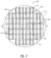
- FIG. 1Ais a top plan view of a microfeature workpiece 100 at an initial stage before the workpiece has been attached to a support member.
- the workpiece 100includes a front side 102 and a back side 104 facing opposite the front side 102 .
- the workpiece 100further includes a plurality of microelectronic components 106 (e.g., microelectronic dies) having active portions 107 (shown schematically in the Figures) positioned at least proximate to the front side 102 of the workpiece 100 .
- the active portions 107can include circuit elements or devices, such as lines, vias, terminals, transistors, data storage elements, image sensors, or other conductor or semiconductor components arranged in an array on the workpiece 100 .
- the individual active portions 107 on the workpiece 100can be separated from each other by a plurality of non-active portions 110 .
- These non-active portions 110are commonly aligned with one another to facilitate cutting with a wafer saw, defining so-called streets or scribe lines 111 between the individual components 106 .
- the active portions 107 and/or non-active portions 110can include other features and/or have other arrangements.
- the non-active portions 110may contain sacrificial active elements (e.g., test or diagnostic elements) that are active during processing of the workpiece 100 , but not active when processing of the workpiece is completed.
- an adhesive material 120is deposited onto one or more of the non-active portions 110 on the front side 102 of the workpiece 100 .
- the adhesive material 120can be a bead of adhesive material deposited onto the non-active portions 110 in a plurality of generally parallel columns 108 and rows 109 (corresponding at least in part to the scribe lines 111 ) that are approximately as wide as a wafer saw or dicing blade that is subsequently used to singulate the workpiece 100 , as discussed in greater detail below with respect to FIG. 1F .
- the adhesive material 120can include an epoxy material or other suitable material. As discussed below, the adhesive material 120 does not need to have any special release characteristics because all or substantially all the adhesive material 120 is removed during the singulation process.
- the adhesive material 120can be deposited onto the front side 102 of the workpiece using a pen-type dispensing process, a screen printing process, a photoetch process, precut strips or grids of adhesive material deposited onto desired portions of the workpiece 100 , a tape dispensing process (e.g., a layer of tape over all or substantially all the front side 102 of the workpiece 100 with cut-out portions corresponding to one or more of the active portions 106 ), or another suitable process known to those of ordinary skill in the art.
- FIG. 1Cis a side cross-sectional view of the workpiece 100 taken along line 1 C- 1 C of FIG. 1B after a sacrificial first support member 130 (e.g., a carrier substrate) is attached at one or more attachment locations 122 on the front side 102 of the workpiece 100 to form a microfeature assembly 140 .
- Each attachment location 122can include a portion of adhesive material 120 to secure the first support member 130 to the workpiece 100 .
- the first support member 130can be glass, quartz, or another material that is at least partially transparent.
- the active portions 107can include image sensors and the first support member 130 can be at least partially transmissive to ultraviolet radiation so that the first support member 130 does not obstruct the image sensors during testing (e.g., illumination of the image sensors).
- the first support member 130can include other suitable materials, including opaque materials.
- the first support member 130can be sized and shaped to receive the workpiece 100 and provide support to the workpiece 100 during subsequent processing steps.
- the first support member 130can be generally rigid and has a planform shape at least approximately identical to that of the workpiece 100 .
- the first support member 130can be slightly larger than the workpiece 100 to avoid the need for precisely aligning the workpiece 100 with the first support member 130 when attaching the two together and for protecting the edge after thinning.
- the additional processingcan include removing material from the back side 104 of the workpiece 100 to reduce its thickness.
- FIG. 1Dis a side cross-sectional view of the assembly 140 after the workpiece 100 has been thinned. More specifically, the workpiece 100 has been thinned from a first thickness T 1 (shown in broken lines) to a second thickness T 2 less than the first thickness T 1 .
- the materialcan be removed from the back side 104 by grinding and/or etching. In other embodiments, the material can be removed from the back side 104 in accordance with other existing processes.
- the first support member 130can provide sufficient support to the workpiece 100 to prevent it from breaking and/or excessively warping during processing.
- the thickness of the assembly 140 after it has been thinnedmay be slightly greater than that of a conventional microfeature workpiece, but the overall size and shape of the assembly 140 can be generally the same as the size and shape of conventional microfeature workpieces. Accordingly, the equipment and steps used to process the workpiece 100 with the first support member 130 attached can be similar or identical to the equipment and steps used to process existing microfeature workpieces.
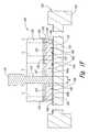
- the assembly 140can be inverted and attached as a unit to a second support member 150 .
- the second support member 150can include an existing dicing support having a frame 152 carrying a replaceable film 153 that can include an attachment device 154 (e.g., tape) that releasably adheres to the back side 104 of the workpiece 100 . Accordingly, the second support member 150 can support the back side 104 of the workpiece 100 , while the first support member 130 continues to provide support for the front side 102 of the workpiece 100 .
- an attachment device 154e.g., tape
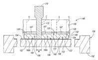
- the assembly 140can be diced, singulated, or otherwise separated to produce a plurality of microelectronic dies 160 , including a first die 160 a and a second die 160 b , separated by incisions C.
- a wafer saw 170can be used to form the incisions C.
- the saw 170can cut through the first support member 130 , the adhesive material 120 , the workpiece 100 , and in some cases at least a portion of the attachment device 154 .
- the motion of the first support member 130can be controlled during singulation to avoid damage to the dies 160 .
- the wafer saw 170includes a blade 172 having a width W corresponding at least in part to the width of the non-active portions 110 ( FIG. 1B ) on the workpiece 100 .
- the width W of the blade 172is at least as wide as the width of the adhesive material 120 deposited onto the non-active portion 110 between the first die 160 a and the second die 160 b so that all or substantially all the adhesive material 120 is removed from the assembly 140 during the singulation process.
- the width W of the blade 172may be narrower than the width of the adhesive material 120 between the first die 160 a and the second die 160 b , and a suitable post-processing cleaning step can be used to remove the remaining adhesive material 120 from the dies 160 .
- a conventional pick-and-place apparatus 180can be used to remove the first die 160 a from the remainder of the assembly 140 .
- the attachment device 154remains attached to the film 153 so that no portion of the attachment device 154 is removed with the first die 160 a .
- at least a portion of the attachment device 154can be removed along with the first die 160 a , and can later be removed from the first die 160 a in a separate step.
- the first die 160 acan be removed from the second support member 150 while the second die 160 b remains proximate to the second support member 150 .
- the foregoing removal processcan then be repeated from the second die 160 b and other dies 160 .
- a release agente.g., ultraviolet radiation
- the dies 160can undergo further packaging and/or processing steps.
- the adhesive material 120is applied to non-active portions 110 of the workpiece 100 . Accordingly, all or at least approximately all the adhesive material 120 is removed from the workpiece 100 during singulation.
- An advantage of this featureis that the adhesive material 120 does not need to have any special release characteristics or require any post-processing cleaning to remove adhesive material residue from the singulated dies. Accordingly, the various components of the dies 160 are less likely to be contaminated and/or damaged as compared to conventional processes that require heat, solvents, and/or post-processing cleaning to remove the adhesive material 120 from the workpiece 100 .
- first support member 130can remain attached to the workpiece 100 as the workpiece is thinned and attached to the second support member 150 .
- An advantage of this featureis that the workpiece 100 can be less likely to be damaged or broken as it is transferred from a grinder or other thickness-reducing tool to the second support member 150 .
- the first support member 130can also provide a generally rigid support structure that reduces the likelihood for the workpiece 100 to bend or warp during additional processing.
- Still another feature of embodiments of the method described aboveis that the first support member 130 is releasably attached to the front side 102 of the workpiece 100 over all or substantially all the active portions 107 of the workpiece 100 .
- An advantage of this featureis that the active portions 107 of the workpiece 100 are less likely to be damaged as the workpiece 100 is processed because the first support member 130 provides support and protection.
- the first support member 130can shield the active portions 107 from incidental contact with surrounding tools, machinery, and/or other components.
- FIG. 2illustrates a stage in a method of releasably attaching a support member to a microfeature workpiece in accordance with another embodiment of the invention. More specifically, FIG. 2 is a top plan view of the workpiece 100 after an adhesive material 220 has been deposited onto the workpiece 100 .
- This stage of this methoddiffers from the stages described above in that the adhesive material 220 deposited on the front side 102 of the workpiece 100 is applied in only one direction (as shown by arrows V), as opposed to the bi-directional application of the adhesive material 120 described above with respect to FIG. 1B .
- One advantage of applying the adhesive material 220 in only one directionis that the adhesive material 220 is less likely to build up at intersections 112 of the scribe lines 111 on the workpiece 100 . Excessive build-up of the adhesive material can result in additional residue on the workpiece after singulation that can contaminate the active portions 107 and/or require additional post-processing removal.
- the adhesive material 220may be deposited onto the workpiece 100 in other directions, patterns, and/or arrangements. After applying the adhesive material 220 , the workpiece 100 can undergo additional processing steps that are at least generally similar to those described above with reference to FIGS. 1C-1G .
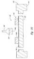
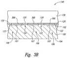
- FIGS. 3A and 3Billustrate stages in a method of releasably attaching a support member to a microfeature workpiece in accordance with still another embodiment of the invention. More particularly, FIG. 3A is a top plan view of the workpiece 100 after a removable cover material 300 has been deposited onto the front side 102 of the workpiece 100 and selectively removed using a masking process or other suitable process, leaving the remaining portions of the cover material 300 only on the active portions 107 .
- the removable cover material 300can include a photoresist or other selectively removable substance. As discussed below, the remaining cover material portions 300 can protect the active portions 107 of the workpiece 100 during subsequent processing steps.
- FIG. 3Bis a side cross-sectional view of the workpiece 100 taken along line 3 B- 3 B of FIG. 3A after the first support member 130 is attached to the workpiece 100 to form the microfeature assembly 140 .
- the cover material portions 300fill the gaps between the first support member 130 and the active portions 106 of the workpiece 100 .
- the cover material 300can protect the active portions 107 during singulation or subsequent processing procedures.
- the cover material 300can protect the active portions 107 from fluids and particulates while dicing the first support member 130 and the workpiece 100 , as described above with respect to FIG. 1F .
- the cover material 300can be removed from the workpiece 100 either during or after the various processing steps described above.
Landscapes
- Engineering & Computer Science (AREA)
- Physics & Mathematics (AREA)
- Condensed Matter Physics & Semiconductors (AREA)
- General Physics & Mathematics (AREA)
- Manufacturing & Machinery (AREA)
- Computer Hardware Design (AREA)
- Microelectronics & Electronic Packaging (AREA)
- Power Engineering (AREA)
- Dicing (AREA)
- Container, Conveyance, Adherence, Positioning, Of Wafer (AREA)
Abstract
Description
Claims (17)
Priority Applications (1)
| Application Number | Priority Date | Filing Date | Title |
|---|---|---|---|
| US11/585,485US7833601B2 (en) | 2005-07-19 | 2006-10-24 | Methods for releasably attaching support members to microfeature workpieces and microfeature assemblies formed using such methods |
Applications Claiming Priority (2)
| Application Number | Priority Date | Filing Date | Title |
|---|---|---|---|
| US11/185,045US7169248B1 (en) | 2005-07-19 | 2005-07-19 | Methods for releasably attaching support members to microfeature workpieces and microfeature assemblies formed using such methods |
| US11/585,485US7833601B2 (en) | 2005-07-19 | 2006-10-24 | Methods for releasably attaching support members to microfeature workpieces and microfeature assemblies formed using such methods |
Related Parent Applications (1)
| Application Number | Title | Priority Date | Filing Date |
|---|---|---|---|
| US11/185,045DivisionUS7169248B1 (en) | 2005-07-19 | 2005-07-19 | Methods for releasably attaching support members to microfeature workpieces and microfeature assemblies formed using such methods |
Publications (2)
| Publication Number | Publication Date |
|---|---|
| US20070036932A1 US20070036932A1 (en) | 2007-02-15 |
| US7833601B2true US7833601B2 (en) | 2010-11-16 |
Family
ID=37677987
Family Applications (2)
| Application Number | Title | Priority Date | Filing Date |
|---|---|---|---|
| US11/185,045Expired - LifetimeUS7169248B1 (en) | 2005-07-19 | 2005-07-19 | Methods for releasably attaching support members to microfeature workpieces and microfeature assemblies formed using such methods |
| US11/585,485Active2027-04-14US7833601B2 (en) | 2005-07-19 | 2006-10-24 | Methods for releasably attaching support members to microfeature workpieces and microfeature assemblies formed using such methods |
Family Applications Before (1)
| Application Number | Title | Priority Date | Filing Date |
|---|---|---|---|
| US11/185,045Expired - LifetimeUS7169248B1 (en) | 2005-07-19 | 2005-07-19 | Methods for releasably attaching support members to microfeature workpieces and microfeature assemblies formed using such methods |
Country Status (1)
| Country | Link |
|---|---|
| US (2) | US7169248B1 (en) |
Families Citing this family (10)
| Publication number | Priority date | Publication date | Assignee | Title |
|---|---|---|---|---|
| US7169248B1 (en)* | 2005-07-19 | 2007-01-30 | Micron Technology, Inc. | Methods for releasably attaching support members to microfeature workpieces and microfeature assemblies formed using such methods |
| JP4830740B2 (en)* | 2005-11-16 | 2011-12-07 | 株式会社デンソー | Manufacturing method of semiconductor chip |
| US8018056B2 (en)* | 2005-12-21 | 2011-09-13 | International Rectifier Corporation | Package for high power density devices |
| US7749349B2 (en)* | 2006-03-14 | 2010-07-06 | Micron Technology, Inc. | Methods and systems for releasably attaching support members to microfeature workpieces |
| JP2008053250A (en)* | 2006-08-22 | 2008-03-06 | Sony Corp | Manufacturing method of semiconductor device |
| SG147330A1 (en) | 2007-04-19 | 2008-11-28 | Micron Technology Inc | Semiconductor workpiece carriers and methods for processing semiconductor workpieces |
| JP2010073235A (en)* | 2008-09-16 | 2010-04-02 | Nec Corp | Method of manufacturing fine-pattern structure, and fine-pattern structure |
| US8772136B2 (en)* | 2012-05-30 | 2014-07-08 | United Microelectronics Corporation | Method for fabricating semiconductor device |
| US9478453B2 (en) | 2014-09-17 | 2016-10-25 | International Business Machines Corporation | Sacrificial carrier dicing of semiconductor wafers |
| KR101913684B1 (en)* | 2016-10-21 | 2018-11-01 | 주식회사 볼트크리에이션 | Appratus for dry etching and method for controlling the same |
Citations (50)
| Publication number | Priority date | Publication date | Assignee | Title |
|---|---|---|---|---|
| US4353952A (en) | 1979-09-28 | 1982-10-12 | Hewlett-Packard Company | Transparent digitizer platen |
| US5170930A (en) | 1991-11-14 | 1992-12-15 | Microelectronics And Computer Technology Corporation | Liquid metal paste for thermal and electrical connections |
| US5591290A (en) | 1995-01-23 | 1997-01-07 | Wallace Computer Services, Inc. | Method of making a laminate having variable adhesive properties |
| US5656552A (en) | 1996-06-24 | 1997-08-12 | Hudak; John James | Method of making a thin conformal high-yielding multi-chip module |
| US5824177A (en) | 1995-07-13 | 1998-10-20 | Nippondenso Co., Ltd. | Method for manufacturing a semiconductor device |
| US5851845A (en) | 1995-12-18 | 1998-12-22 | Micron Technology, Inc. | Process for packaging a semiconductor die using dicing and testing |
| US5866953A (en) | 1996-05-24 | 1999-02-02 | Micron Technology, Inc. | Packaged die on PCB with heat sink encapsulant |
| US5888883A (en) | 1997-07-23 | 1999-03-30 | Kabushiki Kaisha Toshiba | Method of dividing a wafer and method of manufacturing a semiconductor device |
| US5891753A (en) | 1997-01-24 | 1999-04-06 | Micron Technology, Inc. | Method and apparatus for packaging flip chip bare die on printed circuit boards |
| US5933713A (en) | 1998-04-06 | 1999-08-03 | Micron Technology, Inc. | Method of forming overmolded chip scale package and resulting product |
| US5946553A (en) | 1991-06-04 | 1999-08-31 | Micron Technology, Inc. | Process for manufacturing a semiconductor package with bi-substrate die |
| US6004867A (en) | 1996-12-16 | 1999-12-21 | Samsung Electronics Co., Ltd. | Chip-size packages assembled using mass production techniques at the wafer-level |
| US6008070A (en) | 1998-05-21 | 1999-12-28 | Micron Technology, Inc. | Wafer level fabrication and assembly of chip scale packages |
| US6072236A (en) | 1996-03-07 | 2000-06-06 | Micron Technology, Inc. | Micromachined chip scale package |
| EP1041624A1 (en) | 1999-04-02 | 2000-10-04 | Interuniversitair Microelektronica Centrum Vzw | Method of transferring ultra-thin substrates and application of the method to the manufacture of a multilayer thin film device |
| US6184465B1 (en) | 1998-11-12 | 2001-02-06 | Micron Technology, Inc. | Semiconductor package |
| US6187615B1 (en) | 1998-08-28 | 2001-02-13 | Samsung Electronics Co., Ltd. | Chip scale packages and methods for manufacturing the chip scale packages at wafer level |
| US6204079B1 (en) | 1998-07-30 | 2001-03-20 | Commissariat A L'energie Atomique | Selective transfer of elements from one support to another support |
| US6214733B1 (en) | 1999-11-17 | 2001-04-10 | Elo Technologies, Inc. | Process for lift off and handling of thin film materials |
| US6228687B1 (en) | 1999-06-28 | 2001-05-08 | Micron Technology, Inc. | Wafer-level package and methods of fabricating |
| US6232136B1 (en) | 1990-12-31 | 2001-05-15 | Kopin Corporation | Method of transferring semiconductors |
| US6235552B1 (en) | 1999-07-09 | 2001-05-22 | Samsung Electronics Co., Ltd. | Chip scale package and method for manufacturing the same using a redistribution substrate |
| US6310288B1 (en) | 1996-05-21 | 2001-10-30 | Micron Technology, Inc. | Underfill coating for loc package |
| US6320266B1 (en) | 1999-03-18 | 2001-11-20 | Advanced Micro Devices, Inc. | Technique for reducing breakage of thinned flip-chip multi-layer integrated circuit devices |
| US6326698B1 (en) | 2000-06-08 | 2001-12-04 | Micron Technology, Inc. | Semiconductor devices having protective layers thereon through which contact pads are exposed and stereolithographic methods of fabricating such semiconductor devices |
| US6338980B1 (en) | 1999-08-13 | 2002-01-15 | Citizen Watch Co., Ltd. | Method for manufacturing chip-scale package and manufacturing IC chip |
| US6342434B1 (en) | 1995-12-04 | 2002-01-29 | Hitachi, Ltd. | Methods of processing semiconductor wafer, and producing IC card, and carrier |
| US6358354B1 (en) | 2000-07-05 | 2002-03-19 | Lexmark International, Inc. | UV and thermally curable adhesive formulation |
| US20020053735A1 (en) | 2000-09-19 | 2002-05-09 | Neuhaus Herbert J. | Method for assembling components and antennae in radio frequency identification devices |
| US6407381B1 (en) | 2000-07-05 | 2002-06-18 | Amkor Technology, Inc. | Wafer scale image sensor package |
| US6440777B2 (en) | 1997-08-20 | 2002-08-27 | Micron Technology, Inc. | Method of depositing a thermoplastic polymer in semiconductor fabrication |
| US20020185644A1 (en) | 2001-06-07 | 2002-12-12 | Erich Thallner | Device for detaching a carrier from a semi-conductor disk |
| US6503780B1 (en) | 2000-07-05 | 2003-01-07 | Amkor Technology, Inc. | Wafer scale image sensor package fabrication method |
| US6558975B2 (en) | 2000-08-31 | 2003-05-06 | Lintec Corporation | Process for producing semiconductor device |
| US6576531B2 (en) | 2001-08-24 | 2003-06-10 | Micron Technology, Inc. | Method for cutting semiconductor wafers |
| US6576495B1 (en) | 2000-08-30 | 2003-06-10 | Micron Technology, Inc. | Microelectronic assembly with pre-disposed fill material and associated method of manufacture |
| US6642126B2 (en) | 1999-12-22 | 2003-11-04 | Micronas Gmbh | Process for manufacturing a semiconductor wafer with passivation layer mask for etching with mechanical removal |
| US20030209310A1 (en) | 2002-05-13 | 2003-11-13 | Fuentes Anastacio C. | Apparatus, system and method to reduce wafer warpage |
| US6670008B1 (en) | 2002-04-09 | 2003-12-30 | Amanda G. Ognissanti | Tamper-evident label with multiple pressure-sensitive adhesives of different sensitivity |
| US6673649B1 (en) | 2002-07-05 | 2004-01-06 | Micron Technology, Inc. | Microelectronic device packages and methods for controlling the disposition of non-conductive materials in such packages |
| US6798121B2 (en) | 2000-03-17 | 2004-09-28 | Matsushita Electric Industrial Co., Ltd. | Module with built-in electronic elements and method of manufacture thereof |
| US20040242003A1 (en) | 2003-05-26 | 2004-12-02 | Shinko Electric Industries Co., Ltd. | Method for thinning wafer by grinding |
| US6842217B1 (en)* | 2001-08-23 | 2005-01-11 | Cambridge Research And Instrumentation, Inc. | Fabry-perot etalons and tunable filters made using liquid crystal devices as tuning material |
| US6864172B2 (en) | 2002-06-18 | 2005-03-08 | Sanyo Electric Co., Ltd. | Manufacturing method of semiconductor device |
| US6869894B2 (en) | 2002-12-20 | 2005-03-22 | General Chemical Corporation | Spin-on adhesive for temporary wafer coating and mounting to support wafer thinning and backside processing |
| US6896760B1 (en) | 2002-01-16 | 2005-05-24 | Micron Technology, Inc. | Fabrication of stacked microelectronic devices |
| US20050176325A1 (en) | 2002-06-06 | 2005-08-11 | Shoji Tokuda | Electret filter media and process for producing the same |
| US20050176235A1 (en) | 2002-06-18 | 2005-08-11 | Sanyo Electric Co., Ltd. | Manufacturing method of semiconductor device |
| US20060162850A1 (en) | 2005-01-24 | 2006-07-27 | Micron Technology, Inc. | Methods and apparatus for releasably attaching microfeature workpieces to support members |
| US7169248B1 (en) | 2005-07-19 | 2007-01-30 | Micron Technology, Inc. | Methods for releasably attaching support members to microfeature workpieces and microfeature assemblies formed using such methods |
- 2005
- 2005-07-19USUS11/185,045patent/US7169248B1/ennot_activeExpired - Lifetime
- 2006
- 2006-10-24USUS11/585,485patent/US7833601B2/enactiveActive
Patent Citations (59)
| Publication number | Priority date | Publication date | Assignee | Title |
|---|---|---|---|---|
| US4353952A (en) | 1979-09-28 | 1982-10-12 | Hewlett-Packard Company | Transparent digitizer platen |
| US6232136B1 (en) | 1990-12-31 | 2001-05-15 | Kopin Corporation | Method of transferring semiconductors |
| US6020624A (en) | 1991-06-04 | 2000-02-01 | Micron Technology, Inc. | Semiconductor package with bi-substrate die |
| US5946553A (en) | 1991-06-04 | 1999-08-31 | Micron Technology, Inc. | Process for manufacturing a semiconductor package with bi-substrate die |
| US5170930A (en) | 1991-11-14 | 1992-12-15 | Microelectronics And Computer Technology Corporation | Liquid metal paste for thermal and electrical connections |
| US5591290A (en) | 1995-01-23 | 1997-01-07 | Wallace Computer Services, Inc. | Method of making a laminate having variable adhesive properties |
| US5824177A (en) | 1995-07-13 | 1998-10-20 | Nippondenso Co., Ltd. | Method for manufacturing a semiconductor device |
| US6342434B1 (en) | 1995-12-04 | 2002-01-29 | Hitachi, Ltd. | Methods of processing semiconductor wafer, and producing IC card, and carrier |
| US5851845A (en) | 1995-12-18 | 1998-12-22 | Micron Technology, Inc. | Process for packaging a semiconductor die using dicing and testing |
| US6124634A (en) | 1996-03-07 | 2000-09-26 | Micron Technology, Inc. | Micromachined chip scale package |
| US6072236A (en) | 1996-03-07 | 2000-06-06 | Micron Technology, Inc. | Micromachined chip scale package |
| US6310288B1 (en) | 1996-05-21 | 2001-10-30 | Micron Technology, Inc. | Underfill coating for loc package |
| US5866953A (en) | 1996-05-24 | 1999-02-02 | Micron Technology, Inc. | Packaged die on PCB with heat sink encapsulant |
| US5656552A (en) | 1996-06-24 | 1997-08-12 | Hudak; John James | Method of making a thin conformal high-yielding multi-chip module |
| US6004867A (en) | 1996-12-16 | 1999-12-21 | Samsung Electronics Co., Ltd. | Chip-size packages assembled using mass production techniques at the wafer-level |
| US5898224A (en) | 1997-01-24 | 1999-04-27 | Micron Technology, Inc. | Apparatus for packaging flip chip bare die on printed circuit boards |
| US5891753A (en) | 1997-01-24 | 1999-04-06 | Micron Technology, Inc. | Method and apparatus for packaging flip chip bare die on printed circuit boards |
| US5888883A (en) | 1997-07-23 | 1999-03-30 | Kabushiki Kaisha Toshiba | Method of dividing a wafer and method of manufacturing a semiconductor device |
| US6440777B2 (en) | 1997-08-20 | 2002-08-27 | Micron Technology, Inc. | Method of depositing a thermoplastic polymer in semiconductor fabrication |
| US5933713A (en) | 1998-04-06 | 1999-08-03 | Micron Technology, Inc. | Method of forming overmolded chip scale package and resulting product |
| US6008070A (en) | 1998-05-21 | 1999-12-28 | Micron Technology, Inc. | Wafer level fabrication and assembly of chip scale packages |
| US6326697B1 (en) | 1998-05-21 | 2001-12-04 | Micron Technology, Inc. | Hermetically sealed chip scale packages formed by wafer level fabrication and assembly |
| US6204079B1 (en) | 1998-07-30 | 2001-03-20 | Commissariat A L'energie Atomique | Selective transfer of elements from one support to another support |
| US6187615B1 (en) | 1998-08-28 | 2001-02-13 | Samsung Electronics Co., Ltd. | Chip scale packages and methods for manufacturing the chip scale packages at wafer level |
| US6184465B1 (en) | 1998-11-12 | 2001-02-06 | Micron Technology, Inc. | Semiconductor package |
| US6320266B1 (en) | 1999-03-18 | 2001-11-20 | Advanced Micro Devices, Inc. | Technique for reducing breakage of thinned flip-chip multi-layer integrated circuit devices |
| EP1041624A1 (en) | 1999-04-02 | 2000-10-04 | Interuniversitair Microelektronica Centrum Vzw | Method of transferring ultra-thin substrates and application of the method to the manufacture of a multilayer thin film device |
| US6228687B1 (en) | 1999-06-28 | 2001-05-08 | Micron Technology, Inc. | Wafer-level package and methods of fabricating |
| US6235552B1 (en) | 1999-07-09 | 2001-05-22 | Samsung Electronics Co., Ltd. | Chip scale package and method for manufacturing the same using a redistribution substrate |
| US6338980B1 (en) | 1999-08-13 | 2002-01-15 | Citizen Watch Co., Ltd. | Method for manufacturing chip-scale package and manufacturing IC chip |
| US6214733B1 (en) | 1999-11-17 | 2001-04-10 | Elo Technologies, Inc. | Process for lift off and handling of thin film materials |
| US6642126B2 (en) | 1999-12-22 | 2003-11-04 | Micronas Gmbh | Process for manufacturing a semiconductor wafer with passivation layer mask for etching with mechanical removal |
| US6798121B2 (en) | 2000-03-17 | 2004-09-28 | Matsushita Electric Industrial Co., Ltd. | Module with built-in electronic elements and method of manufacture thereof |
| US6326698B1 (en) | 2000-06-08 | 2001-12-04 | Micron Technology, Inc. | Semiconductor devices having protective layers thereon through which contact pads are exposed and stereolithographic methods of fabricating such semiconductor devices |
| US6503780B1 (en) | 2000-07-05 | 2003-01-07 | Amkor Technology, Inc. | Wafer scale image sensor package fabrication method |
| US6407381B1 (en) | 2000-07-05 | 2002-06-18 | Amkor Technology, Inc. | Wafer scale image sensor package |
| US6358354B1 (en) | 2000-07-05 | 2002-03-19 | Lexmark International, Inc. | UV and thermally curable adhesive formulation |
| US6576495B1 (en) | 2000-08-30 | 2003-06-10 | Micron Technology, Inc. | Microelectronic assembly with pre-disposed fill material and associated method of manufacture |
| US6661104B2 (en) | 2000-08-30 | 2003-12-09 | Micron Technology, Inc. | Microelectronic assembly with pre-disposed fill material and associated method of manufacture |
| US6558975B2 (en) | 2000-08-31 | 2003-05-06 | Lintec Corporation | Process for producing semiconductor device |
| US20020053735A1 (en) | 2000-09-19 | 2002-05-09 | Neuhaus Herbert J. | Method for assembling components and antennae in radio frequency identification devices |
| US20020185644A1 (en) | 2001-06-07 | 2002-12-12 | Erich Thallner | Device for detaching a carrier from a semi-conductor disk |
| US6842217B1 (en)* | 2001-08-23 | 2005-01-11 | Cambridge Research And Instrumentation, Inc. | Fabry-perot etalons and tunable filters made using liquid crystal devices as tuning material |
| US6576531B2 (en) | 2001-08-24 | 2003-06-10 | Micron Technology, Inc. | Method for cutting semiconductor wafers |
| US20060172510A1 (en) | 2002-01-16 | 2006-08-03 | Micron Technology, Inc. | Fabrication of stacked microelectronic devices |
| US20060159947A1 (en) | 2002-01-16 | 2006-07-20 | Micron Technology, Inc. | Fabrication of stacked microelectronic devices |
| US7037751B2 (en) | 2002-01-16 | 2006-05-02 | Micron Technology, Inc. | Fabrication of stacked microelectronic devices |
| US7022418B2 (en) | 2002-01-16 | 2006-04-04 | Micron Technology, Inc. | Fabrication of stacked microelectronic devices |
| US6896760B1 (en) | 2002-01-16 | 2005-05-24 | Micron Technology, Inc. | Fabrication of stacked microelectronic devices |
| US6670008B1 (en) | 2002-04-09 | 2003-12-30 | Amanda G. Ognissanti | Tamper-evident label with multiple pressure-sensitive adhesives of different sensitivity |
| US20030209310A1 (en) | 2002-05-13 | 2003-11-13 | Fuentes Anastacio C. | Apparatus, system and method to reduce wafer warpage |
| US20050176325A1 (en) | 2002-06-06 | 2005-08-11 | Shoji Tokuda | Electret filter media and process for producing the same |
| US20050176235A1 (en) | 2002-06-18 | 2005-08-11 | Sanyo Electric Co., Ltd. | Manufacturing method of semiconductor device |
| US6864172B2 (en) | 2002-06-18 | 2005-03-08 | Sanyo Electric Co., Ltd. | Manufacturing method of semiconductor device |
| US6673649B1 (en) | 2002-07-05 | 2004-01-06 | Micron Technology, Inc. | Microelectronic device packages and methods for controlling the disposition of non-conductive materials in such packages |
| US6869894B2 (en) | 2002-12-20 | 2005-03-22 | General Chemical Corporation | Spin-on adhesive for temporary wafer coating and mounting to support wafer thinning and backside processing |
| US20040242003A1 (en) | 2003-05-26 | 2004-12-02 | Shinko Electric Industries Co., Ltd. | Method for thinning wafer by grinding |
| US20060162850A1 (en) | 2005-01-24 | 2006-07-27 | Micron Technology, Inc. | Methods and apparatus for releasably attaching microfeature workpieces to support members |
| US7169248B1 (en) | 2005-07-19 | 2007-01-30 | Micron Technology, Inc. | Methods for releasably attaching support members to microfeature workpieces and microfeature assemblies formed using such methods |
Non-Patent Citations (5)
| Title |
|---|
| Staystik Thermoplastic Adhesives, Application Bulletin, Bulletin #6. Cookson Electronics, Mar. 1, 2001, Retrieved from the Internet: . |
| Staystik Thermoplastic Adhesives, Application Bulletin, Bulletin #6. Cookson Electronics, Mar. 1, 2001, Retrieved from the Internet: <URL http://www.cooksonsemi.com/pdfs/STAYSTIK%20Appl%20Bull-Wafer—2002.pdf>. |
| Sumitomo 3M Ltd., Product Description, H-WSS (Wafer Support System) For Ultra Thin Wafer Backgrinding, 2 pages, Sep. 1, 2003. |
| U.S. Appl. No. 11/185,045, filed Jul. 19, 2005, Kirby et al. |
| U.S. Appl. No. 11/374,750, filed Mar. 14, 2006, Pratt et al. |
Also Published As
| Publication number | Publication date |
|---|---|
| US20070017630A1 (en) | 2007-01-25 |
| US20070036932A1 (en) | 2007-02-15 |
| US7169248B1 (en) | 2007-01-30 |
Similar Documents
| Publication | Publication Date | Title |
|---|---|---|
| US7833601B2 (en) | Methods for releasably attaching support members to microfeature workpieces and microfeature assemblies formed using such methods | |
| US9595504B2 (en) | Methods and systems for releasably attaching support members to microfeature workpieces | |
| US6465329B1 (en) | Microcircuit die-sawing protector and method | |
| US6555417B2 (en) | Method and device for protecting micro electromechanical system structures during dicing of a wafer | |
| US9570314B2 (en) | Methods for singulating semiconductor wafer | |
| US7846776B2 (en) | Methods for releasably attaching sacrificial support members to microfeature workpieces and microfeature devices formed using such methods | |
| US9196520B1 (en) | Tape release systems and methods for semiconductor dies | |
| US20070134471A1 (en) | Methods and apparatuses for releasably attaching microfeature workpieces to support members | |
| TW201921545A (en) | Substrate processing system and substrate processing method | |
| CN105097990B (en) | Method for manufacturing semiconductor structure | |
| US20080242053A1 (en) | Integrated circuit system with a debris trapping system | |
| US8011513B2 (en) | Semiconductor workpiece carriers and methods for processing semiconductor workpieces | |
| CN110718484A (en) | Method for separating integrated circuit packages | |
| EP1238423A2 (en) | Methods for separating microcircuit dies from wafers | |
| KR20200035448A (en) | Substrate processing method and substrate processing apparatus | |
| KR101327528B1 (en) | Wafer chip grinding method | |
| US20080026491A1 (en) | Method of wafer segmenting |
Legal Events
| Date | Code | Title | Description |
|---|---|---|---|
| FEPP | Fee payment procedure | Free format text:PAYOR NUMBER ASSIGNED (ORIGINAL EVENT CODE: ASPN); ENTITY STATUS OF PATENT OWNER: LARGE ENTITY | |
| STCF | Information on status: patent grant | Free format text:PATENTED CASE | |
| FPAY | Fee payment | Year of fee payment:4 | |
| AS | Assignment | Owner name:U.S. BANK NATIONAL ASSOCIATION, AS COLLATERAL AGENT, CALIFORNIA Free format text:SECURITY INTEREST;ASSIGNOR:MICRON TECHNOLOGY, INC.;REEL/FRAME:038669/0001 Effective date:20160426 Owner name:U.S. BANK NATIONAL ASSOCIATION, AS COLLATERAL AGEN Free format text:SECURITY INTEREST;ASSIGNOR:MICRON TECHNOLOGY, INC.;REEL/FRAME:038669/0001 Effective date:20160426 | |
| AS | Assignment | Owner name:MORGAN STANLEY SENIOR FUNDING, INC., AS COLLATERAL AGENT, MARYLAND Free format text:PATENT SECURITY AGREEMENT;ASSIGNOR:MICRON TECHNOLOGY, INC.;REEL/FRAME:038954/0001 Effective date:20160426 Owner name:MORGAN STANLEY SENIOR FUNDING, INC., AS COLLATERAL Free format text:PATENT SECURITY AGREEMENT;ASSIGNOR:MICRON TECHNOLOGY, INC.;REEL/FRAME:038954/0001 Effective date:20160426 | |
| AS | Assignment | Owner name:U.S. BANK NATIONAL ASSOCIATION, AS COLLATERAL AGENT, CALIFORNIA Free format text:CORRECTIVE ASSIGNMENT TO CORRECT THE REPLACE ERRONEOUSLY FILED PATENT #7358718 WITH THE CORRECT PATENT #7358178 PREVIOUSLY RECORDED ON REEL 038669 FRAME 0001. ASSIGNOR(S) HEREBY CONFIRMS THE SECURITY INTEREST;ASSIGNOR:MICRON TECHNOLOGY, INC.;REEL/FRAME:043079/0001 Effective date:20160426 Owner name:U.S. BANK NATIONAL ASSOCIATION, AS COLLATERAL AGEN Free format text:CORRECTIVE ASSIGNMENT TO CORRECT THE REPLACE ERRONEOUSLY FILED PATENT #7358718 WITH THE CORRECT PATENT #7358178 PREVIOUSLY RECORDED ON REEL 038669 FRAME 0001. ASSIGNOR(S) HEREBY CONFIRMS THE SECURITY INTEREST;ASSIGNOR:MICRON TECHNOLOGY, INC.;REEL/FRAME:043079/0001 Effective date:20160426 | |
| MAFP | Maintenance fee payment | Free format text:PAYMENT OF MAINTENANCE FEE, 8TH YEAR, LARGE ENTITY (ORIGINAL EVENT CODE: M1552) Year of fee payment:8 | |
| AS | Assignment | Owner name:JPMORGAN CHASE BANK, N.A., AS COLLATERAL AGENT, ILLINOIS Free format text:SECURITY INTEREST;ASSIGNORS:MICRON TECHNOLOGY, INC.;MICRON SEMICONDUCTOR PRODUCTS, INC.;REEL/FRAME:047540/0001 Effective date:20180703 Owner name:JPMORGAN CHASE BANK, N.A., AS COLLATERAL AGENT, IL Free format text:SECURITY INTEREST;ASSIGNORS:MICRON TECHNOLOGY, INC.;MICRON SEMICONDUCTOR PRODUCTS, INC.;REEL/FRAME:047540/0001 Effective date:20180703 | |
| AS | Assignment | Owner name:MICRON TECHNOLOGY, INC., IDAHO Free format text:RELEASE BY SECURED PARTY;ASSIGNOR:U.S. BANK NATIONAL ASSOCIATION, AS COLLATERAL AGENT;REEL/FRAME:047243/0001 Effective date:20180629 | |
| AS | Assignment | Owner name:MICRON TECHNOLOGY, INC., IDAHO Free format text:RELEASE BY SECURED PARTY;ASSIGNOR:MORGAN STANLEY SENIOR FUNDING, INC., AS COLLATERAL AGENT;REEL/FRAME:050937/0001 Effective date:20190731 | |
| AS | Assignment | Owner name:MICRON SEMICONDUCTOR PRODUCTS, INC., IDAHO Free format text:RELEASE BY SECURED PARTY;ASSIGNOR:JPMORGAN CHASE BANK, N.A., AS COLLATERAL AGENT;REEL/FRAME:051028/0001 Effective date:20190731 Owner name:MICRON TECHNOLOGY, INC., IDAHO Free format text:RELEASE BY SECURED PARTY;ASSIGNOR:JPMORGAN CHASE BANK, N.A., AS COLLATERAL AGENT;REEL/FRAME:051028/0001 Effective date:20190731 | |
| MAFP | Maintenance fee payment | Free format text:PAYMENT OF MAINTENANCE FEE, 12TH YEAR, LARGE ENTITY (ORIGINAL EVENT CODE: M1553); ENTITY STATUS OF PATENT OWNER: LARGE ENTITY Year of fee payment:12 |