US7833427B2 - Electron beam etching device and method - Google Patents
Electron beam etching device and methodDownload PDFInfo
- Publication number
- US7833427B2 US7833427B2US11/503,681US50368106AUS7833427B2US 7833427 B2US7833427 B2US 7833427B2US 50368106 AUS50368106 AUS 50368106AUS 7833427 B2US7833427 B2US 7833427B2
- Authority
- US
- United States
- Prior art keywords
- gas
- semiconductor surface
- region
- coating
- semiconductor
- Prior art date
- Legal status (The legal status is an assumption and is not a legal conclusion. Google has not performed a legal analysis and makes no representation as to the accuracy of the status listed.)
- Active, expires
Links
- 238000000034methodMethods0.000titleclaimsabstractdescription48
- 238000010894electron beam technologyMethods0.000titleclaimsabstractdescription44
- 238000005530etchingMethods0.000titleclaimsabstractdescription30
- 239000004065semiconductorSubstances0.000claimsabstractdescription90
- OKTJSMMVPCPJKN-UHFFFAOYSA-NCarbonChemical compound[C]OKTJSMMVPCPJKN-UHFFFAOYSA-N0.000claimsabstractdescription30
- 229910052799carbonInorganic materials0.000claimsabstractdescription30
- 229910052736halogenInorganic materials0.000claimsabstractdescription26
- 150000002367halogensChemical class0.000claimsabstractdescription26
- 238000000576coating methodMethods0.000claimsdescription53
- 239000011248coating agentSubstances0.000claimsdescription50
- VYPSYNLAJGMNEJ-UHFFFAOYSA-NSilicium dioxideChemical groupO=[Si]=OVYPSYNLAJGMNEJ-UHFFFAOYSA-N0.000claimsdescription30
- 230000015654memoryEffects0.000claimsdescription23
- XUIMIQQOPSSXEZ-UHFFFAOYSA-NSiliconChemical compound[Si]XUIMIQQOPSSXEZ-UHFFFAOYSA-N0.000claimsdescription16
- 239000002516radical scavengerSubstances0.000claimsdescription16
- 239000010703siliconSubstances0.000claimsdescription16
- 238000000151depositionMethods0.000claimsdescription15
- 229910052710siliconInorganic materials0.000claimsdescription15
- 238000003384imaging methodMethods0.000claimsdescription7
- YCKRFDGAMUMZLT-UHFFFAOYSA-NFluorine atomChemical compound[F]YCKRFDGAMUMZLT-UHFFFAOYSA-N0.000claimsdescription6
- XPDWGBQVDMORPB-UHFFFAOYSA-NFluoroformChemical compoundFC(F)FXPDWGBQVDMORPB-UHFFFAOYSA-N0.000claimsdescription6
- 229910052731fluorineInorganic materials0.000claimsdescription6
- 239000011737fluorineSubstances0.000claimsdescription6
- 229910052814silicon oxideInorganic materials0.000claimsdescription5
- 230000008878couplingEffects0.000claimsdescription4
- 238000010168coupling processMethods0.000claimsdescription4
- 238000005859coupling reactionMethods0.000claimsdescription4
- 229910052756noble gasInorganic materials0.000claimsdescription3
- 238000006243chemical reactionMethods0.000abstractdescription17
- 230000008569processEffects0.000abstractdescription7
- 230000006870functionEffects0.000abstractdescription3
- 239000013626chemical specieSubstances0.000abstract2
- 230000004913activationEffects0.000abstract1
- 239000011253protective coatingSubstances0.000abstract1
- 239000011241protective layerSubstances0.000abstract1
- 239000007789gasSubstances0.000description53
- 239000000463materialSubstances0.000description23
- 239000000758substrateSubstances0.000description15
- 239000000377silicon dioxideSubstances0.000description13
- 230000008901benefitEffects0.000description11
- 238000010586diagramMethods0.000description10
- 235000012431wafersNutrition0.000description10
- 235000012239silicon dioxideNutrition0.000description9
- 238000001514detection methodMethods0.000description8
- 238000004519manufacturing processMethods0.000description7
- 239000000203mixtureSubstances0.000description7
- 238000010494dissociation reactionMethods0.000description5
- 230000005593dissociationsEffects0.000description5
- 239000002245particleSubstances0.000description5
- 238000005033Fourier transform infrared spectroscopyMethods0.000description4
- 229910052681coesiteInorganic materials0.000description4
- 229910052906cristobaliteInorganic materials0.000description4
- 239000012212insulatorSubstances0.000description4
- 230000002093peripheral effectEffects0.000description4
- 229910052682stishoviteInorganic materials0.000description4
- 229910052905tridymiteInorganic materials0.000description4
- UFHFLCQGNIYNRP-UHFFFAOYSA-NHydrogenChemical compound[H][H]UFHFLCQGNIYNRP-UHFFFAOYSA-N0.000description3
- 238000000231atomic layer depositionMethods0.000description3
- 239000000126substanceSubstances0.000description3
- 230000001360synchronised effectEffects0.000description3
- XKRFYHLGVUSROY-UHFFFAOYSA-NArgonChemical compound[Ar]XKRFYHLGVUSROY-UHFFFAOYSA-N0.000description2
- 239000006227byproductSubstances0.000description2
- 239000004020conductorSubstances0.000description2
- 230000001276controlling effectEffects0.000description2
- 239000001257hydrogenSubstances0.000description2
- 229910052739hydrogenInorganic materials0.000description2
- 125000004435hydrogen atomChemical group[H]*0.000description2
- 230000003993interactionEffects0.000description2
- 230000007246mechanismEffects0.000description2
- 238000003672processing methodMethods0.000description2
- 238000003860storageMethods0.000description2
- JBRZTFJDHDCESZ-UHFFFAOYSA-NAsGaChemical compound[As]#[Ga]JBRZTFJDHDCESZ-UHFFFAOYSA-N0.000description1
- WKBOTKDWSSQWDR-UHFFFAOYSA-NBromine atomChemical compound[Br]WKBOTKDWSSQWDR-UHFFFAOYSA-N0.000description1
- ZAMOUSCENKQFHK-UHFFFAOYSA-NChlorine atomChemical compound[Cl]ZAMOUSCENKQFHK-UHFFFAOYSA-N0.000description1
- 229910001218Gallium arsenideInorganic materials0.000description1
- 230000006978adaptationEffects0.000description1
- 229910052786argonInorganic materials0.000description1
- 229910052789astatineInorganic materials0.000description1
- RYXHOMYVWAEKHL-UHFFFAOYSA-Nastatine atomChemical compound[At]RYXHOMYVWAEKHL-UHFFFAOYSA-N0.000description1
- 230000015572biosynthetic processEffects0.000description1
- GDTBXPJZTBHREO-UHFFFAOYSA-NbromineSubstancesBrBrGDTBXPJZTBHREO-UHFFFAOYSA-N0.000description1
- 229910052794bromiumInorganic materials0.000description1
- 239000003990capacitorSubstances0.000description1
- 238000012512characterization methodMethods0.000description1
- 229910052801chlorineInorganic materials0.000description1
- 239000000460chlorineSubstances0.000description1
- 230000008021depositionEffects0.000description1
- 238000005137deposition processMethods0.000description1
- 238000005516engineering processMethods0.000description1
- 239000012467final productSubstances0.000description1
- NBVXSUQYWXRMNV-UHFFFAOYSA-NfluoromethaneChemical compoundFCNBVXSUQYWXRMNV-UHFFFAOYSA-N0.000description1
- 229910052732germaniumInorganic materials0.000description1
- GNPVGFCGXDBREM-UHFFFAOYSA-Ngermanium atomChemical compound[Ge]GNPVGFCGXDBREM-UHFFFAOYSA-N0.000description1
- 239000011521glassSubstances0.000description1
- 229910052734heliumInorganic materials0.000description1
- 239000001307heliumSubstances0.000description1
- SWQJXJOGLNCZEY-UHFFFAOYSA-Nhelium atomChemical compound[He]SWQJXJOGLNCZEY-UHFFFAOYSA-N0.000description1
- PNDPGZBMCMUPRI-UHFFFAOYSA-NiodineChemical compoundIIPNDPGZBMCMUPRI-UHFFFAOYSA-N0.000description1
- 238000010884ion-beam techniqueMethods0.000description1
- 229910052743kryptonInorganic materials0.000description1
- DNNSSWSSYDEUBZ-UHFFFAOYSA-Nkrypton atomChemical compound[Kr]DNNSSWSSYDEUBZ-UHFFFAOYSA-N0.000description1
- 229910052754neonInorganic materials0.000description1
- GKAOGPIIYCISHV-UHFFFAOYSA-Nneon atomChemical compound[Ne]GKAOGPIIYCISHV-UHFFFAOYSA-N0.000description1
- 150000004767nitridesChemical class0.000description1
- 230000000704physical effectEffects0.000description1
- 238000006116polymerization reactionMethods0.000description1
- 230000001681protective effectEffects0.000description1
- 238000010926purgeMethods0.000description1
- 229910052704radonInorganic materials0.000description1
- SYUHGPGVQRZVTB-UHFFFAOYSA-Nradon atomChemical compound[Rn]SYUHGPGVQRZVTB-UHFFFAOYSA-N0.000description1
- 230000001105regulatory effectEffects0.000description1
- 238000004544sputter depositionMethods0.000description1
- 230000003068static effectEffects0.000description1
- 229910052724xenonInorganic materials0.000description1
- FHNFHKCVQCLJFQ-UHFFFAOYSA-Nxenon atomChemical compound[Xe]FHNFHKCVQCLJFQ-UHFFFAOYSA-N0.000description1
Images

Classifications
- H—ELECTRICITY
- H01—ELECTRIC ELEMENTS
- H01L—SEMICONDUCTOR DEVICES NOT COVERED BY CLASS H10
- H01L21/00—Processes or apparatus adapted for the manufacture or treatment of semiconductor or solid state devices or of parts thereof
- H01L21/02—Manufacture or treatment of semiconductor devices or of parts thereof
- H01L21/04—Manufacture or treatment of semiconductor devices or of parts thereof the devices having potential barriers, e.g. a PN junction, depletion layer or carrier concentration layer
- H01L21/18—Manufacture or treatment of semiconductor devices or of parts thereof the devices having potential barriers, e.g. a PN junction, depletion layer or carrier concentration layer the devices having semiconductor bodies comprising elements of Group IV of the Periodic Table or AIIIBV compounds with or without impurities, e.g. doping materials
- H01L21/30—Treatment of semiconductor bodies using processes or apparatus not provided for in groups H01L21/20 - H01L21/26
- H01L21/31—Treatment of semiconductor bodies using processes or apparatus not provided for in groups H01L21/20 - H01L21/26 to form insulating layers thereon, e.g. for masking or by using photolithographic techniques; After treatment of these layers; Selection of materials for these layers
- H01L21/3105—After-treatment
- H01L21/311—Etching the insulating layers by chemical or physical means
- H01L21/31105—Etching inorganic layers
- H01L21/31111—Etching inorganic layers by chemical means
- H01L21/31116—Etching inorganic layers by chemical means by dry-etching
Definitions
- This applicationrelates generally to semiconductor devices and device fabrication and, more particularly, to surface processing using electron beams.
- Semiconductor processingis used to form structures and devices such as transistors, capacitors, etc. that in turn are used to form semiconductor memory chips, processing chips, and other integrated circuits.
- Semiconductor deviceuses range from personal computers, to MP3 music players, to mobile telephones.
- techniques that are frequently usedinclude material deposition processes, and material removal processes such as etching. By sequentially depositing and etching in selected regions on a semiconductor wafer, devices such as transistors, etc. are eventually formed.
- Selectively etching a semiconductor surfaceis a necessary step in most semiconductor processing operations.
- Selectivitycan be obtained using a number of techniques, including use of a protective mask or using chemicals that selectively react with one material over another. Although techniques exist that provide some degree of selectivity, further improvements to processes that reduce time needed to complete a step, and/or eliminate processing steps are desired to further reduce cost. Improving selectivity also provides increased precision, allowing more detailed and/or smaller structure formation.
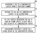
- FIG. 1shows a method flow diagram of semiconductor processing according to an embodiment of the invention.
- FIG. 2shows a side view surface diagram of semiconductor processing according to an embodiment of the invention.
- FIG. 3shows a block diagram of a semiconductor processing system according to an embodiment of the invention.
- FIG. 4shows another diagram of a semiconductor processing system according to an embodiment of the invention.
- FIG. 5shows a block diagram of a semiconductor memory according to an embodiment of the invention.
- FIG. 6shows a block diagram of an electronic system according to an embodiment of the invention.
- wafer and substrate used in the following descriptioninclude any structure having an exposed surface with which to form an integrated circuit (IC) structure.
- substrateis understood to include semiconductor wafers.
- substrateis understood to include semiconductor on insulator wafers such as silicon-on-insulator (SOI).
- SOIsilicon-on-insulator
- substrateis also used to refer to semiconductor structures during processing, and may include other layers that have been fabricated thereupon. Both wafer and substrate include doped and undoped semiconductors, epitaxial semiconductor layers supported by a base semiconductor or insulator, as well as other semiconductor structures well known to one skilled in the art.
- conductoris understood to generally include n-type and p-type semiconductors and the term insulator or dielectric is defined to include any material that is less electrically conductive than the materials referred to as conductors.
- FIG. 1shows a flow diagram with a method of semiconductor surface processing according to one embodiment of the invention.
- a semiconductor surfaceis included within a processing chamber, and a gas is introduced.
- the semiconductor surfaceincludes one or more semiconductor wafers.
- One processing chamberincludes an in-line production chamber where wafers are passed from station to station in a vacuum.
- a processing chamberincludes a chamber of a scanning electron microscope (SEM) as will be discussed in more detail below.
- SEMscanning electron microscope
- the gasincludes a gas capable of dissociating into one or more species capable of etching a region of the semiconductor surface.
- the gasincludes a gas that dissociates when exposed to energies supplied by an electron beam, including, but not limited to a beam in a SEM.
- the gasincludes a halogen species. Examples of halogens include fluorine, chlorine, bromine, iodine, and astatine.
- the gasfurther includes carbon.
- One example of a gas that includes carbon and fluorine as a halogeninclude CF 4 .
- the gasincludes other species such as hydrogen or another element.
- One example of a gas including hydrogenis CHF 3 .
- other species in addition to carbon and a halogeninclude multi-component species such as a carbon and hydrogen chain, or other combination of elements.
- the gasis exposed to an electron beam.
- the electron beamis generated by an electron beam source in an electron microscope such as a SEM.
- the electron beamcan be focused using electromagnetic lenses.
- the SEM configurationalso provides a system to scan the electron beam over an area of the substrate.
- an imaging systemis further included.
- an imaging systemincludes devices such as a secondary electron detector.
- One advantage of a SEM configurationincludes the ability to focus and scan on only a selected portion of the substrate such as a semiconductor wafer.
- Another advantage of a SEM configurationincludes the ability to concurrently image the selected portion of the surface being exposed to the electron beam. The ability to image allows a user to easily select the region to be exposed to the electron beam from the bulk of the semiconductor surface.
- a material composition detection systemis further included.
- material composition detection systemsinclude, but are not limited to x-ray detection systems, Fourier transform infrared (FTIR) detection systems, mass spectrometers, etc.
- FTIRFourier transform infrared
- a material composition detection systemis used to quantify composition of a coating that is grown in conjunction with electron beam interaction. Growth of such coatings will be discussed in more detail below.
- an electron microscopeis used as an example of an electron beam source, the invention is not so limited.
- Other embodimentsinclude an electron beam source without additional microscope elements such as lenses, rastering systems, secondary electron detectors, etc.
- the gasis at least partially dissociated into a number of reactive species.
- the energy from the electron beamprovides at least a portion of the energy necessary to dissociate the gas into the number of reactive species.
- the exact composition of the specieswill depend on the gas that is used. For example, CF 4 gas will dissociate into a number of species such as CF 3 , CF 2 , and CF.
- CF 4 gaswill dissociate into a number of species such as CF 3 , CF 2 , and CF.
- electron beam energyis in a range between 5 eV and 100 eV, although the invention is not so limited.
- One advantage of an electron beam energy range between 5 eV and 100 eV for selected systemsincludes an energy high enough to cause dissociation, yet low enough to not alter surface chemistry and/or structure.
- other energetic beamssuch as neutron beams, x-rays, etc. are used to provide energy appropriate to dissociate the chosen gas.
- Energetic beamssuch as electron beams provide an advantage in selected embodiments because they cause minimal damage to the workpiece in contrast to ion beams or other particle beams that may cause sputtering or other surface damage.
- the gasis chosen such that the reactive species selectively etch a specific material on the semiconductor surface.
- the reactive speciesare chosen to etch silicon dioxide.
- the reactive species generated from the gasdoes not etch a second material such as silicon.
- a selective reactionsuch as etching is determined by a large difference in reaction rate. Although a reaction may be described as occurring on one material and not on another, in one embodiment the reaction may occur on both materials, however a substantial difference in reaction rate is observed.
- a coatingis deposited on a region of the semiconductor surface, while concurrently an etching reaction is occurring on another region of the semiconductor surface.
- One exampleincludes a silicon dioxide region that is adjacent to a silicon region.
- a coatingis deposited on the silicon region while the silicon dioxide region is etched at substantially the same time.
- a coatingis deposited on the silicon dioxide region while the silicon region is etched at substantially the same time.
- silicon and silicon dioxideare used as examples, the invention is not so limited.
- Other semiconductor processing materialscan be selectively etched or coated using appropriate gas chemistry that will be appreciated by one of ordinary skill in the art, having the benefit of the present disclosure. Examples of other semiconductor materials include, but are not limited to nitride materials, spin on glass materials, or other semiconductors such as germanium, or gallium arsenide, etc.
- the coating deposited at step 130includes a carbon containing coating.
- the coatingincludes an amount of halogen.
- the coatingcan be characterized using a ratio of halogen to carbon.
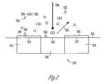
- FIG. 2illustrates one example of a method using some of the examples listed above.
- a gas species 220is shown in a reaction chamber over a substrate 210 .
- the gas species 220includes CHF 3 .
- the substrate 210includes a semiconductor wafer.
- a first silicon region 214 and a second silicon region 216are shown with a silicon dioxide region 218 located adjacent to the silicon regions 214 , 216 .
- An electron beam 230is shown directed at the substrate 210 .
- the electron beam 230is used to image a portion of the substrate 210 , for example, in a SEM device. Additional particles 232 are also shown that are generated as a result of the electron beam 230 interaction with the surface of the substrate 210 . Additional particles 232 include, but are not limited to secondary electrons and backscattered particles. In one embodiment, additional particles are used for imaging and/or material characterization.
- the electron beamis scanned over a surface 212 of the substrate 210 and interacts with the portions of the surface 212 such as silicon regions 214 , 216 and silicon dioxide regions 218 during a scan.
- the electron beam 230is indicated in FIG. 2 as a line, the diameter of the electron beam 230 can vary. In selected embodiments, the electron beam diameter is small and a surface is scanned. In other selected embodiments, the electron beam diameter is large, and a larger surface area of the substrate 210 is covered without scanning. Although it is useful in selected embodiments to have the electron beam contact large regions of the substrate 210 , the invention is not so limited.
- FIG. 2illustrates the gas species 220 as including a first subspecies 222 and a second subspecies 224 .
- the illustration of two subspeciesis used as an example only. In various embodiments, the gas species 220 can be broken down into more than two subspecies.
- the gas 220reacts with the electron beam 230 and is dissociated into the first subspecies 222 and the second subspecies 224 .
- FIG. 2shows the second subspecies 224 etching a surface 219 of the silicon dioxide region 218 . Also shown are a first coating 240 on a top surface 215 of the first silicon region 214 , and a second coating 242 on a top surface 217 of the second silicon region 216 . In a separate reaction, one of the subspecies also forms the coatings. For example, the second subspecies 224 is shown in FIG. 2 forming the first and second coatings 240 , 242 .
- a first subspecies exampleincludes HF and a second subspecies includes CF 2 .
- the CF 2 subspeciesreacts with SiO 2 to form SiOF x and CO x byproducts and the SiO 2 surface, such as surface 219 in FIG. 2 , is etched in the reaction.
- the CF 2 subspeciesdeposits a coating on Si surfaces such as surfaces 215 and 217 of FIG. 2 .
- the coatingis deposited in a polymerization reaction.
- An advantage of forming a coating concurrent to etchingincludes the ability to further enhance selectivity in an etching operation.
- the coatingserves as a sacrificial coating, and further protects the coated surface from etching.
- selective etchingis defined as a large difference in etch rate, with a material such as silicon etching, but at a much slower rate than another adjacent material such as silicon dioxide.
- the presence of a coatingfurther reduces or eliminates any etching of the non selected material.
- Enhanced selectivityprovides a number of advantages including the ability to form more detailed structures with sharper edge profiles, etc.
- the coatingcontains both carbon and an amount of halogen such as fluorine.
- a ratio of halogen to carbonis controlled to tailor the chemical and physical properties of the coating. Controlling the coating chemistry further enhances desired properties such as selective etching. For example, materials with a lower ratio of halogen to carbon provide better resistance to etching.
- the ratio of halogen to carbon in the coatingis controlled by further introducing a scavenger gas to the reaction chamber.
- the scavenger gasis chosen to react with the halogen to form a byproduct gas that is removed from the reaction chamber by the vacuum system. In this way, the amount of halogen is reduced in the coating.
- the scavenger gasincludes hydrogen gas (H 2 ).
- hydrogenforms HF gas, and thus reduces the amount of fluorine available in the chamber to form in the coating.
- a scavenger gasis introduced to remove other species. For example, if it is desirable to have a high ratio of halogen to carbon in a coating, a scavenger gas such as O 2 can be introduced to preferentially remove carbon from the system, forming CO x gasses.
- a noble gasis further introduced to the system.
- noble gassesincludes helium, neon, argon, krypton, xenon, and radon.
- the addition of a noble gasfurther enhances the dissociation of the gas species 220 from FIG. 2 in addition to the dissociation provided by the electron beam 230 .
- One mechanism of enhanced dissociation from noble gassesincludes electron attachment dissociation.
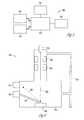
- FIG. 3shows a block diagram of a semiconductor processing system 300 .
- the system 300includes a reaction chamber 310 with an electron beam source 312 coupled to the chamber 310 .
- the electron beam source 312includes a focused scanning electron beam source such as provided in an SEM.
- a vacuum pump 318is shown coupled to the reaction chamber 310 .
- vacuum pumpssuch as mechanical pumps, turbo pumps, etc. are within the scope of the invention.
- a gas supply 316is shown coupled to the reaction chamber 310 .
- the gas supply 316provides one or more gas species in selected amounts.
- One gasincludes a gas species to dissociate into etching and coating species.
- the gas supplyalso provides additional gasses such as scavenger gasses and/or noble gasses as discussed in embodiments above.
- the gas supplyincludes controlling mechanisms and circuitry to function as an atomic layer deposition (ALD) system.
- ALDatomic layer deposition
- selected gassescan be supplied in pulses, and purge gasses or evacuation steps can be included between gas pulses.
- ALDatomic layer deposition
- a detector 314is further included in the system 300 , such as a secondary electron detector.
- the detector 314is used to provide imaging capability to the system 300 such as in a scanning electron microscope configuration.
- other detection capabilityis also included in detector 314 such as detection of elemental composition.
- FIG. 4shows a more detailed diagram of a system 400 similar to the system 300 shown in FIG. 3 .
- the example system 400 in FIG. 4includes a scanning electron type system 400 according to an embodiment of the invention.
- a processing chamber 410is shown with a workpiece 402 .
- the workpieceincludes a semiconductor device, chip, or other component.
- a conduit 418 or other connectionis shown coupling the system 400 to a vacuum device (not shown).
- An electron source 412is included in the system 400 to generate an electron beam 424 directed at a surface of the workpiece 402 .
- a beam focusing lens device 420is included to focus the electron beam 424 .
- a scanning device 422is further included to raster, or otherwise scan a surface of the workpiece 402 with the beam 424 .
- a detector 414is shown coupled to the system 400 .
- the detector 414includes a secondary electron detector as described above to detect secondary electrons 426 as shown in the Figure.
- the detector 414includes other detecting capability such as Fourier transform infrared (FTIR) detection systems, mass spectrometers, etc. for detecting and quantifying material composition.
- FTIRFourier transform infrared
- a gas source 416is shown coupled to the reaction chamber 410 .
- a gas supplied by the gas source 416includes a gas species to dissociate into one or more species that provide etching and coating. In one embodiment, one dissociated species both etches one region and coats another region.
- the gas source 416provides gasses such as scavenger gasses and/or noble gasses as discussed in embodiments above. Specific gasses include, but are not limited to, H 2 , O 2 , noble gasses, and carbon and halogen gasses such as CHF 3 .
- a tube or other directing structure 417is included to better direct the gas or gasses over the workpiece 402 .
- Methods of processing semiconducting wafers, semiconductor devices, IC's, surface, etc. including electron beam techniques as described abovemay be implemented into a wide variety of electronic devices.
- Embodiments of these devicesmay include semiconductor memory, telecommunication systems, wireless systems, and computers. Further, embodiments of electronic devices may be realized as integrated circuits.
- FIG. 5illustrates an example of a semiconductor memory 500 formed using methods and devices described above.
- the memory 500includes an array of memory cells 510 such as dynamic random access memory (DRAM) cells, or flash memory cells.
- a first sense amplifier 530is included in one embodiment.
- a second sense amplifier 532is included in one embodiment.
- Circuitry 520is coupled between cells in the array 510 and one or more sense amplifiers to detect the state of selected cells.
- FIG. 6depicts a diagram of an embodiment of a system 600 having a controller 610 and a memory 630 .
- the controller 610 or memory 630may include structures formed by processes in accordance with the teachings herein.
- System 600also includes an electronic apparatus 640 and a bus 620 , where bus 620 provides electrical conductivity between controller 610 and electronic apparatus 640 , and between controller 610 and memory 630 .
- Bus 620may include an address, a data bus, and a control bus, each independently configured. Alternatively, bus 620 may use common conductive lines for providing address, data, or control, the use of which is regulated by controller 610 .
- electronic apparatus 640may be additional memory configured similar as memory 630 .
- An embodimentmay include an additional peripheral device or devices 650 coupled to bus 620 .
- the controller 610is a processor.
- the controller 610is a processor having a memory. Any of controller 610 , memory 630 , bus 620 , electronic apparatus 640 , and peripheral device devices 650 may include structures formed by processes as described in selected embodiments above.
- System 600may include, but is not limited to, information handling devices, telecommunication systems, and computers.
- Peripheral devices 650may include displays, additional storage memory, or other control devices that may operate in conjunction with controller 610 .
- peripheral devices 650may include displays, additional storage memory, or other control devices that may operate in conjunction with the controller 610 or memory 630 , etc.
- Memory 630may be realized as a memory device containing structures formed by processes in accordance with various embodiments. It will be understood that embodiments are equally applicable to any size and type of memory circuit and are not intended to be limited to a particular type of memory device.
- Memory typesinclude a DRAM, SRAM (Static Random Access Memory) or Flash memories. Additionally, the DRAM could be a synchronous DRAM commonly referred to as SGRAM (Synchronous Graphics Random Access Memory), SDRAM (Synchronous Dynamic Random Access Memory), SDRAM II, and DDR SDRAM (Double Data Rate SDRAM), as well as Synchlink or Rambus DRAMs and other emerging DRAM technologies.
Landscapes
- Engineering & Computer Science (AREA)
- Chemical & Material Sciences (AREA)
- Condensed Matter Physics & Semiconductors (AREA)
- Inorganic Chemistry (AREA)
- Physics & Mathematics (AREA)
- General Chemical & Material Sciences (AREA)
- Chemical Kinetics & Catalysis (AREA)
- General Physics & Mathematics (AREA)
- Manufacturing & Machinery (AREA)
- Computer Hardware Design (AREA)
- Microelectronics & Electronic Packaging (AREA)
- Power Engineering (AREA)
- Drying Of Semiconductors (AREA)
Abstract
Description
Claims (28)
Priority Applications (2)
| Application Number | Priority Date | Filing Date | Title |
|---|---|---|---|
| US11/503,681US7833427B2 (en) | 2006-08-14 | 2006-08-14 | Electron beam etching device and method |
| US12/945,135US20110056625A1 (en) | 2006-08-14 | 2010-11-12 | Electron beam etching device and method |
Applications Claiming Priority (1)
| Application Number | Priority Date | Filing Date | Title |
|---|---|---|---|
| US11/503,681US7833427B2 (en) | 2006-08-14 | 2006-08-14 | Electron beam etching device and method |
Related Child Applications (1)
| Application Number | Title | Priority Date | Filing Date |
|---|---|---|---|
| US12/945,135DivisionUS20110056625A1 (en) | 2006-08-14 | 2010-11-12 | Electron beam etching device and method |
Publications (2)
| Publication Number | Publication Date |
|---|---|
| US20080038928A1 US20080038928A1 (en) | 2008-02-14 |
| US7833427B2true US7833427B2 (en) | 2010-11-16 |
Family
ID=39051341
Family Applications (2)
| Application Number | Title | Priority Date | Filing Date |
|---|---|---|---|
| US11/503,681Active2027-03-03US7833427B2 (en) | 2006-08-14 | 2006-08-14 | Electron beam etching device and method |
| US12/945,135AbandonedUS20110056625A1 (en) | 2006-08-14 | 2010-11-12 | Electron beam etching device and method |
Family Applications After (1)
| Application Number | Title | Priority Date | Filing Date |
|---|---|---|---|
| US12/945,135AbandonedUS20110056625A1 (en) | 2006-08-14 | 2010-11-12 | Electron beam etching device and method |
Country Status (1)
| Country | Link |
|---|---|
| US (2) | US7833427B2 (en) |
Cited By (6)
| Publication number | Priority date | Publication date | Assignee | Title |
|---|---|---|---|---|
| US20100320384A1 (en)* | 2006-07-10 | 2010-12-23 | Williamson Mark J | Method of enhancing detection of defects on a surface |
| US8389415B2 (en) | 2006-08-14 | 2013-03-05 | Micron Technology, Inc. | Profiling solid state samples |
| US8809074B2 (en) | 2006-07-10 | 2014-08-19 | Micron Technology, Inc. | Method for integrated circuit diagnosis |
| US8821682B2 (en) | 2006-07-10 | 2014-09-02 | Micron Technology, Inc. | Electron induced chemical etching and deposition for local circuit repair |
| US9758858B2 (en) | 2012-10-05 | 2017-09-12 | Tyco Electronics Corporation | Methods of manufacturing a coated structure on a substrate |
| US10154595B2 (en) | 2012-10-05 | 2018-12-11 | Te Connectivity Corporation | Electrical components and methods and systems of manufacturing electrical components |
Families Citing this family (8)
| Publication number | Priority date | Publication date | Assignee | Title |
|---|---|---|---|---|
| US7833427B2 (en)* | 2006-08-14 | 2010-11-16 | Micron Technology, Inc. | Electron beam etching device and method |
| US7718080B2 (en)* | 2006-08-14 | 2010-05-18 | Micron Technology, Inc. | Electronic beam processing device and method using carbon nanotube emitter |
| US8778804B2 (en)* | 2009-01-30 | 2014-07-15 | Fei Company | High selectivity, low damage electron-beam delineation etch |
| KR101779349B1 (en)* | 2009-10-14 | 2017-09-18 | 가부시키가이샤 한도오따이 에네루기 켄큐쇼 | Semiconductor device and manufacturing method thereof |
| DE102013012225A1 (en) | 2013-07-23 | 2015-01-29 | Carl Zeiss Microscopy Gmbh | Method for TEM lamella fabrication and assembly for TEM lamellae protection device |
| WO2019226341A1 (en) | 2018-05-25 | 2019-11-28 | Lam Research Corporation | Thermal atomic layer etch with rapid temperature cycling |
| JP7461923B2 (en) | 2018-07-09 | 2024-04-04 | ラム リサーチ コーポレーション | Electron-excited atomic layer etching |
| JP7739434B2 (en) | 2021-02-03 | 2025-09-16 | ラム リサーチ コーポレーション | Control of etching selectivity in atomic layer etching |
Citations (112)
| Publication number | Priority date | Publication date | Assignee | Title |
|---|---|---|---|---|
| US4260649A (en) | 1979-05-07 | 1981-04-07 | The Perkin-Elmer Corporation | Laser induced dissociative chemical gas phase processing of workpieces |
| US4543486A (en) | 1983-05-20 | 1985-09-24 | The United States Of America As Represented By The Secretary Of The Army | Method and apparatus for using a photoacoustic effect for controlling various processes utilizing laser and ion beams, and the like |
| US4579750A (en) | 1980-07-07 | 1986-04-01 | Massachusetts Institute Of Technology | Laser heated CVD process |
| US4581248A (en) | 1984-03-07 | 1986-04-08 | Roche Gregory A | Apparatus and method for laser-induced chemical vapor deposition |
| US4624736A (en)* | 1984-07-24 | 1986-11-25 | The United States Of America As Represented By The United States Department Of Energy | Laser/plasma chemical processing of substrates |
| US4655849A (en) | 1985-05-22 | 1987-04-07 | Eaton Corporation | Semiconductor processing technique for generating dangling surface bonds and growing epitaxial layer by excimer laser |
| US4668304A (en) | 1985-04-10 | 1987-05-26 | Eaton Corporation | Dopant gettering semiconductor processing by excimer laser |
| US4670064A (en) | 1985-04-10 | 1987-06-02 | Eaton Corporation | Generating high purity ions by non-thermal excimer laser processing |
| US4670063A (en) | 1985-04-10 | 1987-06-02 | Eaton Corporation | Semiconductor processing technique with differentially fluxed radiation at incremental thicknesses |
| US4685976A (en) | 1985-04-10 | 1987-08-11 | Eaton Corporation | Multi-layer semiconductor processing with scavenging between layers by excimer laser |
| US4694777A (en) | 1985-07-03 | 1987-09-22 | Roche Gregory A | Apparatus for, and methods of, depositing a substance on a substrate |
| US4832781A (en) | 1988-01-07 | 1989-05-23 | Varian Associates, Inc. | Methods and apparatus for thermal transfer with a semiconductor wafer in vacuum |
| US4933206A (en) | 1988-08-17 | 1990-06-12 | Intel Corporation | UV-vis characteristic writing in silicon nitride and oxynitride films |
| US4938996A (en) | 1988-04-12 | 1990-07-03 | Ziv Alan R | Via filling by selective laser chemical vapor deposition |
| US4940505A (en) | 1988-12-02 | 1990-07-10 | Eaton Corporation | Method for growing single crystalline silicon with intermediate bonding agent and combined thermal and photolytic activation |
| US4980198A (en) | 1989-11-30 | 1990-12-25 | Syracuse University | Laser CVD and plasma CVD of CrO2 films and cobalt doped CrO2 films using organometallic precursors |
| US5032435A (en) | 1989-03-27 | 1991-07-16 | The United States Of America As Represented By The United States Department Of Energy | UV absorption control of thin film growth |
| US5047649A (en) | 1990-10-09 | 1991-09-10 | International Business Machines Corporation | Method and apparatus for writing or etching narrow linewidth patterns on insulating materials |
| US5102830A (en) | 1990-07-24 | 1992-04-07 | Micron Technology, Inc. | Integrated circuit fabrication process for preventing overprocessing during a laser scan |
| US5140164A (en) | 1991-01-14 | 1992-08-18 | Schlumberger Technologies, Inc. | Ic modification with focused ion beam system |
| US5155053A (en) | 1991-05-28 | 1992-10-13 | Hughes Aircraft Company | Method of forming t-gate structure on microelectronic device substrate |
| US5164222A (en) | 1988-02-16 | 1992-11-17 | Mas-Planck-Gesellschaft zur Foerderung der Wissenschaften e.V. | Cvd method for depositing a layer on an electrically conductive thin layer structure |
| US5326981A (en)* | 1991-09-27 | 1994-07-05 | Kawasaki Jukogyo Kabushiki Kaisha | Electron beam excited ion irradiation apparatus |
| US5387443A (en) | 1992-07-09 | 1995-02-07 | Sumitomo Electric Industries, Ltd. | Laser CVD method for synthesizing diamond |
| US5403433A (en) | 1992-07-15 | 1995-04-04 | On-Line Technologies, Inc. | Method and apparatus for monitoring layer processing |
| US5429730A (en) | 1992-11-02 | 1995-07-04 | Kabushiki Kaisha Toshiba | Method of repairing defect of structure |
| US5438019A (en) | 1994-07-11 | 1995-08-01 | Micron Semiconductor, Inc. | Large area thin film growing method |
| US5472935A (en) | 1992-12-01 | 1995-12-05 | Yandrofski; Robert M. | Tuneable microwave devices incorporating high temperature superconducting and ferroelectric films |
| US5508368A (en) | 1994-03-03 | 1996-04-16 | Diamonex, Incorporated | Ion beam process for deposition of highly abrasion-resistant coatings |
| EP0756318A1 (en) | 1995-07-24 | 1997-01-29 | International Business Machines Corporation | Method for real-time in-situ monitoring of a trench formation process |
| US5622567A (en) | 1992-11-30 | 1997-04-22 | Mitsubishi Denki Kabushiki Kaisha | Thin film forming apparatus using laser |
| US5639342A (en) | 1996-03-15 | 1997-06-17 | Taiwan Semiconductor Manufacturing Company Ltd. | Method of monitoring and controlling a silicon nitride etch step |
| US5641545A (en) | 1995-06-07 | 1997-06-24 | Micron Technology, Inc. | Method to deposit highly conformal CVD films |
| US5648114A (en) | 1991-12-13 | 1997-07-15 | Symetrix Corporation | Chemical vapor deposition process for fabricating layered superlattice materials |
| US5682041A (en) | 1992-09-14 | 1997-10-28 | Kabushiki Kaisha Toshiba | Electronic part incorporating artificial super lattice |
| US5733609A (en) | 1993-06-01 | 1998-03-31 | Wang; Liang | Ceramic coatings synthesized by chemical reactions energized by laser plasmas |
| US5754297A (en) | 1994-01-28 | 1998-05-19 | Applied Materials, Inc. | Method and apparatus for monitoring the deposition rate of films during physical vapor deposition |
| US5759923A (en) | 1991-02-25 | 1998-06-02 | Symetrix Corporation | Method and apparatus for fabricating silicon dioxide and silicon glass layers in integrated circuits |
| US5807650A (en) | 1992-03-24 | 1998-09-15 | Kabushiki Kaisha Toshiba | Photo mask and apparatus for repairing photo mask |
| US5825035A (en) | 1993-03-10 | 1998-10-20 | Hitachi, Ltd. | Processing method and apparatus using focused ion beam generating means |
| US5834331A (en) | 1996-10-17 | 1998-11-10 | Northwestern University | Method for making III-Nitride laser and detection device |
| US5942854A (en)* | 1997-06-11 | 1999-08-24 | Kawasaki Jukogyo Kabushiki Kaisha | Electron-beam excited plasma generator with side orifices in the discharge chamber |
| US5976328A (en) | 1996-01-26 | 1999-11-02 | Hitachi, Ltd. | Pattern forming method using charged particle beam process and charged particle beam processing system |
| US5985693A (en) | 1994-09-30 | 1999-11-16 | Elm Technology Corporation | High density three-dimensional IC interconnection |
| US5989928A (en) | 1995-10-20 | 1999-11-23 | Hitachi, Ltd. | Method and device for detecting end point of plasma treatment, method and device for manufacturing semiconductor device, and semiconductor device |
| US6051287A (en) | 1997-06-20 | 2000-04-18 | Micron Technology, Inc. | Laser desorption of CVD precursor species |
| US6064800A (en) | 1996-02-02 | 2000-05-16 | Micron Technology, Inc. | Apparatus for uniform gas and radiant heat dispersion for solid state fabrication processes |
| US6091071A (en) | 1996-04-18 | 2000-07-18 | Sick Ag | Opto-electronic sensor |
| US6113751A (en) | 1998-08-06 | 2000-09-05 | Lockheed Martin Corporation | Electromagnetic beam assisted deposition method for depositing a material on an irradiated substrate |
| US6177147B1 (en)* | 1998-03-27 | 2001-01-23 | Nec Corporation | Process and apparatus for treating a substrate |
| US6187492B1 (en) | 1998-07-07 | 2001-02-13 | Ricoh Company, Ltd. | Electrophotographic photoconductor and method of producing aromatic polycarbonate resin for use in the photoconductor |
| US6194325B1 (en)* | 1992-09-08 | 2001-02-27 | Applied Materials Inc. | Oxide etch process with high selectivity to nitride suitable for use on surfaces of uneven topography |
| US6214183B1 (en) | 1999-01-30 | 2001-04-10 | Advanced Ion Technology, Inc. | Combined ion-source and target-sputtering magnetron and a method for sputtering conductive and nonconductive materials |
| US6281072B1 (en) | 1998-05-11 | 2001-08-28 | Micron Technology, Inc. | Multiple step methods for forming conformal layers |
| US6291341B1 (en) | 1999-02-12 | 2001-09-18 | Micron Technology, Inc. | Method for PECVD deposition of selected material films |
| US6309972B1 (en) | 1998-12-02 | 2001-10-30 | Stmicroelectronics S.R.L. | Method of enhancing protection of dielectrics from plasma induced damages and equipment |
| US6310341B1 (en) | 1998-02-23 | 2001-10-30 | Hitachi, Ltd. | Projecting type charged particle microscope and projecting type substrate inspection system |
| US6462333B1 (en) | 1997-05-29 | 2002-10-08 | Michael S. Gersonde | Apparatus for direct write fabrication of nanostructures |
| US20020173124A1 (en) | 2001-05-18 | 2002-11-21 | Samsung Electronics Co., Ltd. | Method and apparatus for forming multi-layered thin film by using photolysis chemical vapor deposition |
| US20020182542A1 (en) | 2001-06-04 | 2002-12-05 | Choi Won-Bong | Electron emission lithography apparatus and method using a selectively grown carbon nanotube |
| US6499425B1 (en) | 1999-01-22 | 2002-12-31 | Micron Technology, Inc. | Quasi-remote plasma processing method and apparatus |
| US20030047691A1 (en) | 2001-07-27 | 2003-03-13 | Musil Christian R. | Electron beam processing |
| US6573199B2 (en) | 2001-08-30 | 2003-06-03 | Micron Technology, Inc. | Methods of treating dielectric materials with oxygen, and methods of forming capacitor constructions |
| US20030170389A1 (en) | 2002-03-05 | 2003-09-11 | Sandhu Gurtej S. | Atomic layer deposition with point of use generated reactive gas species |
| US20030201391A1 (en) | 1999-09-01 | 2003-10-30 | Hiroyuki Shinada | Method of inspecting a circuit pattern and inspecting instrument |
| EP1363164A1 (en) | 2002-05-16 | 2003-11-19 | NaWoTec GmbH | Procedure for etching of materials at the surface with focussed electron beam induced chemical reactions at said surface |
| US6661005B1 (en) | 1998-11-09 | 2003-12-09 | Fraunhofer-Gesellschaft zur Förderung der angewandten Forschung e.V. | Method of examining and/or modifying surface structures of a sample |
| US20040036398A1 (en) | 2002-08-23 | 2004-02-26 | Sungho Jin | MEMS-based two-dimensional e-beam nano lithography device and method for making the same |
| US20040048398A1 (en) | 2001-06-29 | 2004-03-11 | Ted Liang | Mask repair with electron beam-induced chemical etching |
| US20040091638A1 (en) | 2000-11-13 | 2004-05-13 | International Business Machines Corporation | Method and apparatus for performing laser CVD |
| US20040097076A1 (en) | 2002-11-14 | 2004-05-20 | Iyer Subramanyam A. | Controlled use of photochemically susceptible chemistries for etching, cleaning and surface conditioning |
| US20040113097A1 (en) | 2002-12-17 | 2004-06-17 | International Business Machines Corporation | Apparatus and techniques for scanning electron beam based chip repair |
| US20040124348A1 (en) | 2000-03-15 | 2004-07-01 | Utz Arthur L | Controlling surface chemistry on solid substrates |
| US6764856B2 (en) | 2002-05-02 | 2004-07-20 | Bradley Jay Holmes | Semen detection system and method |
| US20040151991A1 (en) | 2002-09-18 | 2004-08-05 | Stewart Diane K. | Photolithography mask repair |
| JP2004257845A (en) | 2003-02-26 | 2004-09-16 | Renesas Technology Corp | Defect classification method |
| US6793736B2 (en) | 2001-11-30 | 2004-09-21 | Micron Technology, Inc. | Method of providing high flux of point of use activated reactive species for semiconductor processing |
| US6797337B2 (en) | 2002-08-19 | 2004-09-28 | Micron Technology, Inc. | Method for delivering precursors |
| US6809317B2 (en) | 2001-12-06 | 2004-10-26 | Interuniversitair Microelektronica Centrum (Imec) | Method and apparatus for local surface analysis |
| US6811615B2 (en) | 2001-05-24 | 2004-11-02 | Applied Materials, Inc. | Photo-assisted chemical cleaning and laser ablation cleaning of process chamber |
| US6838114B2 (en) | 2002-05-24 | 2005-01-04 | Micron Technology, Inc. | Methods for controlling gas pulsing in processes for depositing materials onto micro-device workpieces |
| US6838121B2 (en) | 2001-05-10 | 2005-01-04 | Zyvex Corporation | System and method for controlling deposition parameters in producing a surface to tune the surface's plasmon resonance wavelength |
| US6845734B2 (en) | 2002-04-11 | 2005-01-25 | Micron Technology, Inc. | Deposition apparatuses configured for utilizing phased microwave radiation |
| US6869479B2 (en) | 2002-03-29 | 2005-03-22 | Altair Center, Llc | Method of laser-assisted fabrication of optoelectronic and photonic components |
| US20050078462A1 (en) | 2003-10-10 | 2005-04-14 | Micron Technology, Inc. | Laser assisted material deposition |
| US20050087514A1 (en) | 2003-08-28 | 2005-04-28 | Hans Koops | Method for high-resolution processing of thin layers using electron beams |
| US6897907B2 (en) | 2001-11-26 | 2005-05-24 | Kabushiki Kaisha Toshiba | Liquid crystal display device and method of manufacturing the same |
| US6911832B2 (en) | 2003-07-16 | 2005-06-28 | Texas Instruments Incorporated | Focused ion beam endpoint detection using charge pulse detection electronics |
| US20050212092A1 (en) | 2004-03-26 | 2005-09-29 | Nec Electronics Corporation | Wafer, semiconductor chip, and semiconductor device manufacturing method |
| US20050266168A1 (en) | 2004-01-30 | 2005-12-01 | Poullos Mark P | Dual laser coating apparatus and process |
| US20060134920A1 (en)* | 2004-12-17 | 2006-06-22 | Ted Liang | Passivating metal etch structures |
| US20060147814A1 (en)* | 2005-01-03 | 2006-07-06 | Ted Liang | Methods for repairing an alternating phase-shift mask |
| US20060154477A1 (en) | 2005-01-12 | 2006-07-13 | Quain Geng | Polymer spacer formation |
| US20060183055A1 (en) | 2005-02-15 | 2006-08-17 | O'neill Mark L | Method for defining a feature on a substrate |
| US20060201911A1 (en) | 2003-06-17 | 2006-09-14 | Lam Research Corporation | Methods of etching photoresist on substrates |
| US7113276B1 (en) | 1996-09-10 | 2006-09-26 | Asti Operating Company, Inc. | Micro defects in semi-conductors |
| US20060228634A1 (en)* | 2005-04-08 | 2006-10-12 | Fei Company | Beam-induced etching |
| US7122125B2 (en) | 2002-11-04 | 2006-10-17 | Applied Materials, Inc. | Controlled polymerization on plasma reactor wall |
| US20070158303A1 (en)* | 2006-01-12 | 2007-07-12 | Kla-Tencor Technologies Corporation | Structural modification using electron beam activated chemical etch |
| US20070158304A1 (en)* | 2006-01-12 | 2007-07-12 | Kla-Tencor Technologies Corporation | Etch selectivity enhancement in electron beam activated chemical etch |
| US7256405B2 (en)* | 2004-01-20 | 2007-08-14 | Ebara Corporation | Sample repairing apparatus, a sample repairing method and a device manufacturing method using the same method |
| US20070228296A1 (en) | 2006-04-03 | 2007-10-04 | Mouttet Blaise L | Parallel Electron Beam Lithography stamp (PEBLS) |
| US20070228002A1 (en) | 2006-03-31 | 2007-10-04 | Qiquan Geng | Simultaneous selective polymer deposition and etch pitch doubling for sub 50nm line/space patterning |
| US7303690B2 (en) | 2004-08-31 | 2007-12-04 | Tokyo Electron Limited | Microlens forming method |
| US20070278180A1 (en)* | 2006-06-01 | 2007-12-06 | Williamson Mark J | Electron induced chemical etching for materials characterization |
| US20080006603A1 (en)* | 2006-07-10 | 2008-01-10 | Micron Technology, Inc. | Electron induced chemical etching and deposition for local circuit repair |
| US20080009140A1 (en)* | 2006-07-10 | 2008-01-10 | Micron Technology, Inc. | Electron induced chemical etching for device level diagnosis |
| US20080006786A1 (en)* | 2006-07-10 | 2008-01-10 | Micron Technology, Inc. | Electron induced chemical etching/deposition for enhanced detection of surface defects |
| US20080038933A1 (en)* | 2006-08-14 | 2008-02-14 | Micron Technology, Inc. | Plasma and electron beam etching device and method |
| US20080038863A1 (en) | 2006-08-14 | 2008-02-14 | Micron Technology, Inc. | Profiling solid state samples |
| US20080038894A1 (en)* | 2006-08-14 | 2008-02-14 | Micron Technology, Inc. | Electronic beam processing device and method using carbon nanotube emitter |
| US7452477B2 (en) | 2002-10-16 | 2008-11-18 | Nawotec Gmbh | Procedure for etching of materials at the surface with focussed electron beam induced chemical reaction at said surface |
Family Cites Families (15)
| Publication number | Priority date | Publication date | Assignee | Title |
|---|---|---|---|---|
| JP2757546B2 (en)* | 1990-08-27 | 1998-05-25 | 日本電気株式会社 | Method and apparatus for etching Fe-containing material |
| TW473857B (en)* | 1996-04-26 | 2002-01-21 | Hitachi Ltd | Method of manufacturing semiconductor device |
| JP2000208488A (en)* | 1999-01-12 | 2000-07-28 | Kawasaki Steel Corp | Etching method |
| US6937447B2 (en)* | 2001-09-19 | 2005-08-30 | Kabushiki Kaisha Toshiba | Magnetoresistance effect element, its manufacturing method, magnetic reproducing element and magnetic memory |
| US20040018739A1 (en)* | 2002-07-26 | 2004-01-29 | Applied Materials, Inc. | Methods for etching using building blocks |
| US6843927B2 (en)* | 2002-08-27 | 2005-01-18 | Kla-Tencor Technologies Corporation | Method and apparatus for endpoint detection in electron beam assisted etching |
| JP3672900B2 (en)* | 2002-09-11 | 2005-07-20 | 松下電器産業株式会社 | Pattern formation method |
| US7365909B2 (en)* | 2002-10-17 | 2008-04-29 | Xradia, Inc. | Fabrication methods for micro compounds optics |
| US7001529B2 (en)* | 2002-10-18 | 2006-02-21 | Lam Research Corporation | Pre-endpoint techniques in photoresist etching |
| US6891169B2 (en)* | 2003-01-21 | 2005-05-10 | International Business Machines Corporation | Electron beam array write head system and method |
| TWI240422B (en)* | 2004-10-29 | 2005-09-21 | Promos Technologies Inc | Method of preparing for structural analysis of deep trench capacitors and structural analysis method thereof |
| US7271107B2 (en)* | 2005-02-03 | 2007-09-18 | Lam Research Corporation | Reduction of feature critical dimensions using multiple masks |
| US7262555B2 (en)* | 2005-03-17 | 2007-08-28 | Micron Technology, Inc. | Method and system for discretely controllable plasma processing |
| US8546264B2 (en)* | 2005-06-02 | 2013-10-01 | The Regents Of The University Of California | Etching radical controlled gas chopped deep reactive ion etching |
| US7833427B2 (en)* | 2006-08-14 | 2010-11-16 | Micron Technology, Inc. | Electron beam etching device and method |
- 2006
- 2006-08-14USUS11/503,681patent/US7833427B2/enactiveActive
- 2010
- 2010-11-12USUS12/945,135patent/US20110056625A1/ennot_activeAbandoned
Patent Citations (133)
| Publication number | Priority date | Publication date | Assignee | Title |
|---|---|---|---|---|
| US4260649A (en) | 1979-05-07 | 1981-04-07 | The Perkin-Elmer Corporation | Laser induced dissociative chemical gas phase processing of workpieces |
| US4579750A (en) | 1980-07-07 | 1986-04-01 | Massachusetts Institute Of Technology | Laser heated CVD process |
| US4543486A (en) | 1983-05-20 | 1985-09-24 | The United States Of America As Represented By The Secretary Of The Army | Method and apparatus for using a photoacoustic effect for controlling various processes utilizing laser and ion beams, and the like |
| US4581248A (en) | 1984-03-07 | 1986-04-08 | Roche Gregory A | Apparatus and method for laser-induced chemical vapor deposition |
| US4624736A (en)* | 1984-07-24 | 1986-11-25 | The United States Of America As Represented By The United States Department Of Energy | Laser/plasma chemical processing of substrates |
| US4670063A (en) | 1985-04-10 | 1987-06-02 | Eaton Corporation | Semiconductor processing technique with differentially fluxed radiation at incremental thicknesses |
| US4668304A (en) | 1985-04-10 | 1987-05-26 | Eaton Corporation | Dopant gettering semiconductor processing by excimer laser |
| US4670064A (en) | 1985-04-10 | 1987-06-02 | Eaton Corporation | Generating high purity ions by non-thermal excimer laser processing |
| US4685976A (en) | 1985-04-10 | 1987-08-11 | Eaton Corporation | Multi-layer semiconductor processing with scavenging between layers by excimer laser |
| US4655849A (en) | 1985-05-22 | 1987-04-07 | Eaton Corporation | Semiconductor processing technique for generating dangling surface bonds and growing epitaxial layer by excimer laser |
| US4694777A (en) | 1985-07-03 | 1987-09-22 | Roche Gregory A | Apparatus for, and methods of, depositing a substance on a substrate |
| US4832781A (en) | 1988-01-07 | 1989-05-23 | Varian Associates, Inc. | Methods and apparatus for thermal transfer with a semiconductor wafer in vacuum |
| US5164222A (en) | 1988-02-16 | 1992-11-17 | Mas-Planck-Gesellschaft zur Foerderung der Wissenschaften e.V. | Cvd method for depositing a layer on an electrically conductive thin layer structure |
| US4938996A (en) | 1988-04-12 | 1990-07-03 | Ziv Alan R | Via filling by selective laser chemical vapor deposition |
| US4933206A (en) | 1988-08-17 | 1990-06-12 | Intel Corporation | UV-vis characteristic writing in silicon nitride and oxynitride films |
| US4940505A (en) | 1988-12-02 | 1990-07-10 | Eaton Corporation | Method for growing single crystalline silicon with intermediate bonding agent and combined thermal and photolytic activation |
| US5032435A (en) | 1989-03-27 | 1991-07-16 | The United States Of America As Represented By The United States Department Of Energy | UV absorption control of thin film growth |
| US4980198A (en) | 1989-11-30 | 1990-12-25 | Syracuse University | Laser CVD and plasma CVD of CrO2 films and cobalt doped CrO2 films using organometallic precursors |
| US5102830A (en) | 1990-07-24 | 1992-04-07 | Micron Technology, Inc. | Integrated circuit fabrication process for preventing overprocessing during a laser scan |
| US5047649A (en) | 1990-10-09 | 1991-09-10 | International Business Machines Corporation | Method and apparatus for writing or etching narrow linewidth patterns on insulating materials |
| US5140164A (en) | 1991-01-14 | 1992-08-18 | Schlumberger Technologies, Inc. | Ic modification with focused ion beam system |
| US5759923A (en) | 1991-02-25 | 1998-06-02 | Symetrix Corporation | Method and apparatus for fabricating silicon dioxide and silicon glass layers in integrated circuits |
| US5155053A (en) | 1991-05-28 | 1992-10-13 | Hughes Aircraft Company | Method of forming t-gate structure on microelectronic device substrate |
| US5326981A (en)* | 1991-09-27 | 1994-07-05 | Kawasaki Jukogyo Kabushiki Kaisha | Electron beam excited ion irradiation apparatus |
| US5648114A (en) | 1991-12-13 | 1997-07-15 | Symetrix Corporation | Chemical vapor deposition process for fabricating layered superlattice materials |
| US5807650A (en) | 1992-03-24 | 1998-09-15 | Kabushiki Kaisha Toshiba | Photo mask and apparatus for repairing photo mask |
| US5387443A (en) | 1992-07-09 | 1995-02-07 | Sumitomo Electric Industries, Ltd. | Laser CVD method for synthesizing diamond |
| US5403433A (en) | 1992-07-15 | 1995-04-04 | On-Line Technologies, Inc. | Method and apparatus for monitoring layer processing |
| US6194325B1 (en)* | 1992-09-08 | 2001-02-27 | Applied Materials Inc. | Oxide etch process with high selectivity to nitride suitable for use on surfaces of uneven topography |
| US5682041A (en) | 1992-09-14 | 1997-10-28 | Kabushiki Kaisha Toshiba | Electronic part incorporating artificial super lattice |
| US5429730A (en) | 1992-11-02 | 1995-07-04 | Kabushiki Kaisha Toshiba | Method of repairing defect of structure |
| US5622567A (en) | 1992-11-30 | 1997-04-22 | Mitsubishi Denki Kabushiki Kaisha | Thin film forming apparatus using laser |
| US5472935A (en) | 1992-12-01 | 1995-12-05 | Yandrofski; Robert M. | Tuneable microwave devices incorporating high temperature superconducting and ferroelectric films |
| US5825035A (en) | 1993-03-10 | 1998-10-20 | Hitachi, Ltd. | Processing method and apparatus using focused ion beam generating means |
| US5733609A (en) | 1993-06-01 | 1998-03-31 | Wang; Liang | Ceramic coatings synthesized by chemical reactions energized by laser plasmas |
| US5754297A (en) | 1994-01-28 | 1998-05-19 | Applied Materials, Inc. | Method and apparatus for monitoring the deposition rate of films during physical vapor deposition |
| US5508368A (en) | 1994-03-03 | 1996-04-16 | Diamonex, Incorporated | Ion beam process for deposition of highly abrasion-resistant coatings |
| US5438019A (en) | 1994-07-11 | 1995-08-01 | Micron Semiconductor, Inc. | Large area thin film growing method |
| US5985693A (en) | 1994-09-30 | 1999-11-16 | Elm Technology Corporation | High density three-dimensional IC interconnection |
| US5641545A (en) | 1995-06-07 | 1997-06-24 | Micron Technology, Inc. | Method to deposit highly conformal CVD films |
| US5800617A (en) | 1995-06-07 | 1998-09-01 | Micron Technology, Inc. | Method to deposit highly conformal CVD films |
| EP0756318A1 (en) | 1995-07-24 | 1997-01-29 | International Business Machines Corporation | Method for real-time in-situ monitoring of a trench formation process |
| US5989928A (en) | 1995-10-20 | 1999-11-23 | Hitachi, Ltd. | Method and device for detecting end point of plasma treatment, method and device for manufacturing semiconductor device, and semiconductor device |
| US5976328A (en) | 1996-01-26 | 1999-11-02 | Hitachi, Ltd. | Pattern forming method using charged particle beam process and charged particle beam processing system |
| US6064800A (en) | 1996-02-02 | 2000-05-16 | Micron Technology, Inc. | Apparatus for uniform gas and radiant heat dispersion for solid state fabrication processes |
| US5639342A (en) | 1996-03-15 | 1997-06-17 | Taiwan Semiconductor Manufacturing Company Ltd. | Method of monitoring and controlling a silicon nitride etch step |
| US6091071A (en) | 1996-04-18 | 2000-07-18 | Sick Ag | Opto-electronic sensor |
| US7113276B1 (en) | 1996-09-10 | 2006-09-26 | Asti Operating Company, Inc. | Micro defects in semi-conductors |
| US5834331A (en) | 1996-10-17 | 1998-11-10 | Northwestern University | Method for making III-Nitride laser and detection device |
| US6462333B1 (en) | 1997-05-29 | 2002-10-08 | Michael S. Gersonde | Apparatus for direct write fabrication of nanostructures |
| US5942854A (en)* | 1997-06-11 | 1999-08-24 | Kawasaki Jukogyo Kabushiki Kaisha | Electron-beam excited plasma generator with side orifices in the discharge chamber |
| US6051287A (en) | 1997-06-20 | 2000-04-18 | Micron Technology, Inc. | Laser desorption of CVD precursor species |
| US6143085A (en) | 1997-06-20 | 2000-11-07 | Micron Technology, Inc. | Laser desorption of CVD precursor species |
| US6310341B1 (en) | 1998-02-23 | 2001-10-30 | Hitachi, Ltd. | Projecting type charged particle microscope and projecting type substrate inspection system |
| US6177147B1 (en)* | 1998-03-27 | 2001-01-23 | Nec Corporation | Process and apparatus for treating a substrate |
| US6281072B1 (en) | 1998-05-11 | 2001-08-28 | Micron Technology, Inc. | Multiple step methods for forming conformal layers |
| US6187492B1 (en) | 1998-07-07 | 2001-02-13 | Ricoh Company, Ltd. | Electrophotographic photoconductor and method of producing aromatic polycarbonate resin for use in the photoconductor |
| US6113751A (en) | 1998-08-06 | 2000-09-05 | Lockheed Martin Corporation | Electromagnetic beam assisted deposition method for depositing a material on an irradiated substrate |
| US6661005B1 (en) | 1998-11-09 | 2003-12-09 | Fraunhofer-Gesellschaft zur Förderung der angewandten Forschung e.V. | Method of examining and/or modifying surface structures of a sample |
| US6309972B1 (en) | 1998-12-02 | 2001-10-30 | Stmicroelectronics S.R.L. | Method of enhancing protection of dielectrics from plasma induced damages and equipment |
| US6499425B1 (en) | 1999-01-22 | 2002-12-31 | Micron Technology, Inc. | Quasi-remote plasma processing method and apparatus |
| US6214183B1 (en) | 1999-01-30 | 2001-04-10 | Advanced Ion Technology, Inc. | Combined ion-source and target-sputtering magnetron and a method for sputtering conductive and nonconductive materials |
| US6291341B1 (en) | 1999-02-12 | 2001-09-18 | Micron Technology, Inc. | Method for PECVD deposition of selected material films |
| US20030201391A1 (en) | 1999-09-01 | 2003-10-30 | Hiroyuki Shinada | Method of inspecting a circuit pattern and inspecting instrument |
| US20040124348A1 (en) | 2000-03-15 | 2004-07-01 | Utz Arthur L | Controlling surface chemistry on solid substrates |
| US20040091638A1 (en) | 2000-11-13 | 2004-05-13 | International Business Machines Corporation | Method and apparatus for performing laser CVD |
| US6838121B2 (en) | 2001-05-10 | 2005-01-04 | Zyvex Corporation | System and method for controlling deposition parameters in producing a surface to tune the surface's plasmon resonance wavelength |
| US20020173124A1 (en) | 2001-05-18 | 2002-11-21 | Samsung Electronics Co., Ltd. | Method and apparatus for forming multi-layered thin film by using photolysis chemical vapor deposition |
| US6811615B2 (en) | 2001-05-24 | 2004-11-02 | Applied Materials, Inc. | Photo-assisted chemical cleaning and laser ablation cleaning of process chamber |
| US20020182542A1 (en) | 2001-06-04 | 2002-12-05 | Choi Won-Bong | Electron emission lithography apparatus and method using a selectively grown carbon nanotube |
| US20040048398A1 (en) | 2001-06-29 | 2004-03-11 | Ted Liang | Mask repair with electron beam-induced chemical etching |
| US20030047691A1 (en) | 2001-07-27 | 2003-03-13 | Musil Christian R. | Electron beam processing |
| US6753538B2 (en)* | 2001-07-27 | 2004-06-22 | Fei Company | Electron beam processing |
| US6613702B2 (en) | 2001-08-30 | 2003-09-02 | Micron Technology, Inc. | Methods of forming capacitor constructions |
| US6683005B2 (en) | 2001-08-30 | 2004-01-27 | Micron Technology, Inc. | Method of forming capacitor constructions |
| US6720272B2 (en) | 2001-08-30 | 2004-04-13 | Micron Technology, Inc. | Methods of forming capacitor constructions |
| US6573199B2 (en) | 2001-08-30 | 2003-06-03 | Micron Technology, Inc. | Methods of treating dielectric materials with oxygen, and methods of forming capacitor constructions |
| US6897907B2 (en) | 2001-11-26 | 2005-05-24 | Kabushiki Kaisha Toshiba | Liquid crystal display device and method of manufacturing the same |
| US6793736B2 (en) | 2001-11-30 | 2004-09-21 | Micron Technology, Inc. | Method of providing high flux of point of use activated reactive species for semiconductor processing |
| US6809317B2 (en) | 2001-12-06 | 2004-10-26 | Interuniversitair Microelektronica Centrum (Imec) | Method and apparatus for local surface analysis |
| US20030170389A1 (en) | 2002-03-05 | 2003-09-11 | Sandhu Gurtej S. | Atomic layer deposition with point of use generated reactive gas species |
| US6730367B2 (en) | 2002-03-05 | 2004-05-04 | Micron Technology, Inc. | Atomic layer deposition method with point of use generated reactive gas species |
| US6869479B2 (en) | 2002-03-29 | 2005-03-22 | Altair Center, Llc | Method of laser-assisted fabrication of optoelectronic and photonic components |
| US6845734B2 (en) | 2002-04-11 | 2005-01-25 | Micron Technology, Inc. | Deposition apparatuses configured for utilizing phased microwave radiation |
| US6764856B2 (en) | 2002-05-02 | 2004-07-20 | Bradley Jay Holmes | Semen detection system and method |
| EP1363164A1 (en) | 2002-05-16 | 2003-11-19 | NaWoTec GmbH | Procedure for etching of materials at the surface with focussed electron beam induced chemical reactions at said surface |
| US7238294B2 (en)* | 2002-05-16 | 2007-07-03 | Nawotec Gmbh | Procedure for etching of materials at the surface with focussed electron beam induced chemical reactions at said surface |
| US6838114B2 (en) | 2002-05-24 | 2005-01-04 | Micron Technology, Inc. | Methods for controlling gas pulsing in processes for depositing materials onto micro-device workpieces |
| US6797337B2 (en) | 2002-08-19 | 2004-09-28 | Micron Technology, Inc. | Method for delivering precursors |
| US20040036398A1 (en) | 2002-08-23 | 2004-02-26 | Sungho Jin | MEMS-based two-dimensional e-beam nano lithography device and method for making the same |
| US20040151991A1 (en) | 2002-09-18 | 2004-08-05 | Stewart Diane K. | Photolithography mask repair |
| US7452477B2 (en) | 2002-10-16 | 2008-11-18 | Nawotec Gmbh | Procedure for etching of materials at the surface with focussed electron beam induced chemical reaction at said surface |
| US7122125B2 (en) | 2002-11-04 | 2006-10-17 | Applied Materials, Inc. | Controlled polymerization on plasma reactor wall |
| US20040097076A1 (en) | 2002-11-14 | 2004-05-20 | Iyer Subramanyam A. | Controlled use of photochemically susceptible chemistries for etching, cleaning and surface conditioning |
| US6787783B2 (en) | 2002-12-17 | 2004-09-07 | International Business Machines Corporation | Apparatus and techniques for scanning electron beam based chip repair |
| US20040113097A1 (en) | 2002-12-17 | 2004-06-17 | International Business Machines Corporation | Apparatus and techniques for scanning electron beam based chip repair |
| JP2004257845A (en) | 2003-02-26 | 2004-09-16 | Renesas Technology Corp | Defect classification method |
| US20060201911A1 (en) | 2003-06-17 | 2006-09-14 | Lam Research Corporation | Methods of etching photoresist on substrates |
| US6911832B2 (en) | 2003-07-16 | 2005-06-28 | Texas Instruments Incorporated | Focused ion beam endpoint detection using charge pulse detection electronics |
| US20050087514A1 (en) | 2003-08-28 | 2005-04-28 | Hans Koops | Method for high-resolution processing of thin layers using electron beams |
| US20060289969A1 (en) | 2003-10-10 | 2006-12-28 | Micron Technology, Inc. | Laser assisted material deposition |
| US20050078462A1 (en) | 2003-10-10 | 2005-04-14 | Micron Technology, Inc. | Laser assisted material deposition |
| US7311947B2 (en) | 2003-10-10 | 2007-12-25 | Micron Technology, Inc. | Laser assisted material deposition |
| US20060288937A1 (en) | 2003-10-10 | 2006-12-28 | Micron Technology, Inc. | Laser assisted material deposition |
| US7256405B2 (en)* | 2004-01-20 | 2007-08-14 | Ebara Corporation | Sample repairing apparatus, a sample repairing method and a device manufacturing method using the same method |
| US20050266168A1 (en) | 2004-01-30 | 2005-12-01 | Poullos Mark P | Dual laser coating apparatus and process |
| US20050212092A1 (en) | 2004-03-26 | 2005-09-29 | Nec Electronics Corporation | Wafer, semiconductor chip, and semiconductor device manufacturing method |
| US7303690B2 (en) | 2004-08-31 | 2007-12-04 | Tokyo Electron Limited | Microlens forming method |
| US20060134920A1 (en)* | 2004-12-17 | 2006-06-22 | Ted Liang | Passivating metal etch structures |
| US20060147814A1 (en)* | 2005-01-03 | 2006-07-06 | Ted Liang | Methods for repairing an alternating phase-shift mask |
| US20060154477A1 (en) | 2005-01-12 | 2006-07-13 | Quain Geng | Polymer spacer formation |
| US20060183055A1 (en) | 2005-02-15 | 2006-08-17 | O'neill Mark L | Method for defining a feature on a substrate |
| US20060228634A1 (en)* | 2005-04-08 | 2006-10-12 | Fei Company | Beam-induced etching |
| US20070158303A1 (en)* | 2006-01-12 | 2007-07-12 | Kla-Tencor Technologies Corporation | Structural modification using electron beam activated chemical etch |
| US20070158304A1 (en)* | 2006-01-12 | 2007-07-12 | Kla-Tencor Technologies Corporation | Etch selectivity enhancement in electron beam activated chemical etch |
| US20070228002A1 (en) | 2006-03-31 | 2007-10-04 | Qiquan Geng | Simultaneous selective polymer deposition and etch pitch doubling for sub 50nm line/space patterning |
| US20070228296A1 (en) | 2006-04-03 | 2007-10-04 | Mouttet Blaise L | Parallel Electron Beam Lithography stamp (PEBLS) |
| US20070278180A1 (en)* | 2006-06-01 | 2007-12-06 | Williamson Mark J | Electron induced chemical etching for materials characterization |
| WO2008008156A2 (en) | 2006-07-10 | 2008-01-17 | Micron Technolgy, Inc. | Electron induced chemical etching for device diagnosis |
| WO2008008159A3 (en) | 2006-07-10 | 2008-04-10 | Micron Technology Inc | Electron induced chemical etching and deposition for circuit repair |
| US20080009140A1 (en)* | 2006-07-10 | 2008-01-10 | Micron Technology, Inc. | Electron induced chemical etching for device level diagnosis |
| WO2008008157A2 (en) | 2006-07-10 | 2008-01-17 | Micron Technology, Inc. | Electron induced chemical etching for detecting defects |
| WO2008008159A2 (en) | 2006-07-10 | 2008-01-17 | Micron Technology, Inc. | Electron induced chemical etching and deposition for circuit repair |
| US20080006603A1 (en)* | 2006-07-10 | 2008-01-10 | Micron Technology, Inc. | Electron induced chemical etching and deposition for local circuit repair |
| WO2008008157A3 (en) | 2006-07-10 | 2008-05-29 | Micron Technology Inc | Electron induced chemical etching for detecting defects |
| US20080006786A1 (en)* | 2006-07-10 | 2008-01-10 | Micron Technology, Inc. | Electron induced chemical etching/deposition for enhanced detection of surface defects |
| WO2008008156A3 (en) | 2006-07-10 | 2008-03-06 | Micron Technolgy Inc | Electron induced chemical etching for device diagnosis |
| WO2008021363A2 (en) | 2006-08-14 | 2008-02-21 | Micron Technology, Inc. | Electron beam processing method using carbon nanotube emitter |
| US20080038894A1 (en)* | 2006-08-14 | 2008-02-14 | Micron Technology, Inc. | Electronic beam processing device and method using carbon nanotube emitter |
| US20080038863A1 (en) | 2006-08-14 | 2008-02-14 | Micron Technology, Inc. | Profiling solid state samples |
| WO2008021363A3 (en) | 2006-08-14 | 2008-08-07 | Micron Technology Inc | Electron beam processing method using carbon nanotube emitter |
| US20080038933A1 (en)* | 2006-08-14 | 2008-02-14 | Micron Technology, Inc. | Plasma and electron beam etching device and method |
| US7569484B2 (en)* | 2006-08-14 | 2009-08-04 | Micron Technology, Inc. | Plasma and electron beam etching device and method |
Non-Patent Citations (15)
| Title |
|---|
| Abramo, M. T, et al., "The application of advanced techniques for complex focused-ion-beam device modification", Reliability of electron devices, failure physics and analysis, 1996. Proceedings of the 7th europeon symposium on Oct. 8-11, 1996, Piscataway, NJ, USA, IEEE, (Oct. 8, 1996), 1775-1778 pgs. |
| Abramo, M., et al., "Gas Assisted Etching: An Advanced Technique for Focused Ion Beam Device Modification", Proceedings of the International Symposium for Testing Failure Analysis, (Nov. 13, 1994), 439-446 pgs. |
| Alers, G., et al., "Interlevel Dielectric Failure in Cooper/Low-K Structures", IEEE, Transactions on Devices and Material Reliability 36, (2004), 148-152, Jun. 2004. |
| Fujii, Toshiaki , et al., "A nanofactory by focused ion beam", Journal of Micromechanics and Microengineering, 15(10), (2005),S286-S291, Sep. 6, 2005. |
| Fujioka, H., et al., "Measurements of the Energy Dependence of Electron Beam Assisted Etching of, and Deposition on, Silica", Journal of Physics D. Applied Physics, IOP Publishing, Bristol, GB, vol. 23, No. 2, (Feb. 14, 1990), 266-268 pgs. |
| Golub, M., "Scanning electron microscope investigations of highly conducting organic compoisites", Journal of Material Sciences 36, (2001), 5543-5550. |
| Jonge, N., et al., "High brightness electron beam from a multi-walled carbon nanotube", Nature vol. 420, (Nov. 28, 2002), 393-395. |
| Liao, J. Y, et al., "Etch characterization of packaged IC samples in an RIE with endpoint detection by ICP source for failure analysis applications", Physical and failure analysis of integrated circuits, 2005, IPFA 2005. Proceedings of the 12th International Symposium on the Shangri-LA's RASA Sentosa Resort, Singapore Jun. 27-Jul. 1, 2005 Piscataway, NJ, USA, IEEE, (Jun. 27, 2005), 123-126 pgs. |
| Marcoux, P. J, et al., "Methods of end point detection for plasma etching", Solid State Technology, Pennwell Corporation, Tulsa, OK, US, vol. 25, (Apr. 1981), 115-122 pgs. |
| Numajiri, T., et al., "Sample Preparation for electron beam testing with reactive ion etching", Physical and Failure Analysis of integrated circuits, 1997, Proceedings of the 1997 6th International Symposium on Sigapore Jul. 21-25, 1997, New york, USA, (Jul. 21, 1997), 56-61 pgs. |
| Randolph, S., et al., "Focused electron-beam-induced etching of silicon dioxide", Journal of Applied Physics, American Institute of Physics, 98, (Aug. 3, 2005), 34902-34902. |
| Sanchez, E. J, et al., "Ion and electron beam assisted growth of nanometric sl m on structures for near-field microscopy", Review of scientific instruments, AIP, Melville, NY, US, vol. 73, No. 11, (Nov. 2002), 3901-3907 pgs. |
| Teo, K., et al., "Fabrication and Electrical Characteristics of carbon nanotube-based microcathodes for use in a parallel elecron-beam lithography system", Journal of Vacuum Science & Technology B: Microelectronics Processing and Phenomena, vol. 21, (Mar. 2003), 693-697. |
| Wang, J , et al., "Etching characteristics of chromium thin films by an electron beam induced surface reaction", Semicond. Sci. Technol., 18, (2003),199-205, Feb. 10, 2003. |
| Wood, L., "Plasma Cleaning of Chip Scale Packages for Improvement of Wire Bond Strength", IEEE, International Symposium on Electronic Materials and Packaging, (2000), 406-408. |
Cited By (8)
| Publication number | Priority date | Publication date | Assignee | Title |
|---|---|---|---|---|
| US20100320384A1 (en)* | 2006-07-10 | 2010-12-23 | Williamson Mark J | Method of enhancing detection of defects on a surface |
| US8026501B2 (en) | 2006-07-10 | 2011-09-27 | Micron Technology, Inc. | Method of removing or deposting material on a surface including material selected to decorate a particle on the surface for imaging |
| US8809074B2 (en) | 2006-07-10 | 2014-08-19 | Micron Technology, Inc. | Method for integrated circuit diagnosis |
| US8821682B2 (en) | 2006-07-10 | 2014-09-02 | Micron Technology, Inc. | Electron induced chemical etching and deposition for local circuit repair |
| US8389415B2 (en) | 2006-08-14 | 2013-03-05 | Micron Technology, Inc. | Profiling solid state samples |
| US8609542B2 (en) | 2006-08-14 | 2013-12-17 | Micron Technology, Inc. | Profiling solid state samples |
| US9758858B2 (en) | 2012-10-05 | 2017-09-12 | Tyco Electronics Corporation | Methods of manufacturing a coated structure on a substrate |
| US10154595B2 (en) | 2012-10-05 | 2018-12-11 | Te Connectivity Corporation | Electrical components and methods and systems of manufacturing electrical components |
Also Published As
| Publication number | Publication date |
|---|---|
| US20110056625A1 (en) | 2011-03-10 |
| US20080038928A1 (en) | 2008-02-14 |
Similar Documents
| Publication | Publication Date | Title |
|---|---|---|
| US7833427B2 (en) | Electron beam etching device and method | |
| US7718080B2 (en) | Electronic beam processing device and method using carbon nanotube emitter | |
| US7569484B2 (en) | Plasma and electron beam etching device and method | |
| US8987139B2 (en) | Method of patterning a low-k dielectric film | |
| US9947549B1 (en) | Cobalt-containing material removal | |
| US11302519B2 (en) | Method of patterning a low-k dielectric film | |
| US7955870B2 (en) | Dry etch stop process for eliminating electrical shorting in MRAM device structures | |
| US10615116B2 (en) | Surface nitridation in metal interconnects | |
| US11367832B2 (en) | Method of making magnetoresistive random access memory device | |
| US11877519B2 (en) | Semiconductor device manufacturing method | |
| US6335284B1 (en) | Metallization process for manufacturing semiconductor devices | |
| KR20230057348A (en) | etching method | |
| US20040110389A1 (en) | Plasma etch method for forming plasma etched silicon layer | |
| US6521544B1 (en) | Method of forming an ultra thin dielectric film | |
| Hussain et al. | Metal wet etch issues and effects in dual metal gate stack integration | |
| US20250308894A1 (en) | Hardmask for high aspect ratio dielectric etch at cryo and elevated temperatures | |
| US20070202704A1 (en) | Method for etching platinum and method for fabricating capacitor using the same | |
| US8748260B2 (en) | Method for manufacturing nano-crystalline silicon material for semiconductor integrated circuits | |
| JP2005167114A (en) | Method and apparatus for forming boron nitride film | |
| Carter et al. | Surface residue island nucleation in anhydrous HF/Alcohol vapor processing of Si surfaces | |
| US20090197421A1 (en) | Chemistry and compositions for manufacturing integrated circuits | |
| US8685826B2 (en) | Method for manufacturing nano-crystalline silicon material from chloride chemistries for the semiconductor integrated circuits | |
| JPH03114225A (en) | Manufacture of semiconductor device |
Legal Events
| Date | Code | Title | Description |
|---|---|---|---|
| AS | Assignment | Owner name:MICRON TECHNOLOGY, INC., IDAHO Free format text:ASSIGNMENT OF ASSIGNORS INTEREST;ASSIGNORS:RUEGER, NEAL R.;WILLIAMSON, MARK J.;SANDHU, GURTEJ S.;REEL/FRAME:018201/0180;SIGNING DATES FROM 20060809 TO 20060810 Owner name:MICRON TECHNOLOGY, INC., IDAHO Free format text:ASSIGNMENT OF ASSIGNORS INTEREST;ASSIGNORS:RUEGER, NEAL R.;WILLIAMSON, MARK J.;SANDHU, GURTEJ S.;SIGNING DATES FROM 20060809 TO 20060810;REEL/FRAME:018201/0180 | |
| FEPP | Fee payment procedure | Free format text:PAYOR NUMBER ASSIGNED (ORIGINAL EVENT CODE: ASPN); ENTITY STATUS OF PATENT OWNER: LARGE ENTITY | |
| STCF | Information on status: patent grant | Free format text:PATENTED CASE | |
| FPAY | Fee payment | Year of fee payment:4 | |
| AS | Assignment | Owner name:U.S. BANK NATIONAL ASSOCIATION, AS COLLATERAL AGENT, CALIFORNIA Free format text:SECURITY INTEREST;ASSIGNOR:MICRON TECHNOLOGY, INC.;REEL/FRAME:038669/0001 Effective date:20160426 Owner name:U.S. BANK NATIONAL ASSOCIATION, AS COLLATERAL AGEN Free format text:SECURITY INTEREST;ASSIGNOR:MICRON TECHNOLOGY, INC.;REEL/FRAME:038669/0001 Effective date:20160426 | |
| AS | Assignment | Owner name:MORGAN STANLEY SENIOR FUNDING, INC., AS COLLATERAL AGENT, MARYLAND Free format text:PATENT SECURITY AGREEMENT;ASSIGNOR:MICRON TECHNOLOGY, INC.;REEL/FRAME:038954/0001 Effective date:20160426 Owner name:MORGAN STANLEY SENIOR FUNDING, INC., AS COLLATERAL Free format text:PATENT SECURITY AGREEMENT;ASSIGNOR:MICRON TECHNOLOGY, INC.;REEL/FRAME:038954/0001 Effective date:20160426 | |
| AS | Assignment | Owner name:U.S. BANK NATIONAL ASSOCIATION, AS COLLATERAL AGENT, CALIFORNIA Free format text:CORRECTIVE ASSIGNMENT TO CORRECT THE REPLACE ERRONEOUSLY FILED PATENT #7358718 WITH THE CORRECT PATENT #7358178 PREVIOUSLY RECORDED ON REEL 038669 FRAME 0001. ASSIGNOR(S) HEREBY CONFIRMS THE SECURITY INTEREST;ASSIGNOR:MICRON TECHNOLOGY, INC.;REEL/FRAME:043079/0001 Effective date:20160426 Owner name:U.S. BANK NATIONAL ASSOCIATION, AS COLLATERAL AGEN Free format text:CORRECTIVE ASSIGNMENT TO CORRECT THE REPLACE ERRONEOUSLY FILED PATENT #7358718 WITH THE CORRECT PATENT #7358178 PREVIOUSLY RECORDED ON REEL 038669 FRAME 0001. ASSIGNOR(S) HEREBY CONFIRMS THE SECURITY INTEREST;ASSIGNOR:MICRON TECHNOLOGY, INC.;REEL/FRAME:043079/0001 Effective date:20160426 | |
| MAFP | Maintenance fee payment | Free format text:PAYMENT OF MAINTENANCE FEE, 8TH YEAR, LARGE ENTITY (ORIGINAL EVENT CODE: M1552) Year of fee payment:8 | |
| AS | Assignment | Owner name:JPMORGAN CHASE BANK, N.A., AS COLLATERAL AGENT, ILLINOIS Free format text:SECURITY INTEREST;ASSIGNORS:MICRON TECHNOLOGY, INC.;MICRON SEMICONDUCTOR PRODUCTS, INC.;REEL/FRAME:047540/0001 Effective date:20180703 Owner name:JPMORGAN CHASE BANK, N.A., AS COLLATERAL AGENT, IL Free format text:SECURITY INTEREST;ASSIGNORS:MICRON TECHNOLOGY, INC.;MICRON SEMICONDUCTOR PRODUCTS, INC.;REEL/FRAME:047540/0001 Effective date:20180703 | |
| AS | Assignment | Owner name:MICRON TECHNOLOGY, INC., IDAHO Free format text:RELEASE BY SECURED PARTY;ASSIGNOR:U.S. BANK NATIONAL ASSOCIATION, AS COLLATERAL AGENT;REEL/FRAME:047243/0001 Effective date:20180629 | |
| AS | Assignment | Owner name:MICRON TECHNOLOGY, INC., IDAHO Free format text:RELEASE BY SECURED PARTY;ASSIGNOR:MORGAN STANLEY SENIOR FUNDING, INC., AS COLLATERAL AGENT;REEL/FRAME:050937/0001 Effective date:20190731 | |
| AS | Assignment | Owner name:MICRON SEMICONDUCTOR PRODUCTS, INC., IDAHO Free format text:RELEASE BY SECURED PARTY;ASSIGNOR:JPMORGAN CHASE BANK, N.A., AS COLLATERAL AGENT;REEL/FRAME:051028/0001 Effective date:20190731 Owner name:MICRON TECHNOLOGY, INC., IDAHO Free format text:RELEASE BY SECURED PARTY;ASSIGNOR:JPMORGAN CHASE BANK, N.A., AS COLLATERAL AGENT;REEL/FRAME:051028/0001 Effective date:20190731 | |
| MAFP | Maintenance fee payment | Free format text:PAYMENT OF MAINTENANCE FEE, 12TH YEAR, LARGE ENTITY (ORIGINAL EVENT CODE: M1553); ENTITY STATUS OF PATENT OWNER: LARGE ENTITY Year of fee payment:12 |