US7831135B2 - Method and system for controlling bake plate temperature in a semiconductor processing chamber - Google Patents
Method and system for controlling bake plate temperature in a semiconductor processing chamberDownload PDFInfo
- Publication number
- US7831135B2 US7831135B2US11/849,978US84997807AUS7831135B2US 7831135 B2US7831135 B2US 7831135B2US 84997807 AUS84997807 AUS 84997807AUS 7831135 B2US7831135 B2US 7831135B2
- Authority
- US
- United States
- Prior art keywords
- temperature
- bake
- face plate
- plate
- wafer
- Prior art date
- Legal status (The legal status is an assumption and is not a legal conclusion. Google has not performed a legal analysis and makes no representation as to the accuracy of the status listed.)
- Active, expires
Links
- 238000000034methodMethods0.000titleclaimsabstractdescription74
- 239000004065semiconductorSubstances0.000titleclaimsabstractdescription14
- 238000012545processingMethods0.000titleabstractdescription42
- 230000004044responseEffects0.000claimsabstractdescription17
- 230000008569processEffects0.000claimsdescription34
- 238000010438heat treatmentMethods0.000claimsdescription16
- 230000008859changeEffects0.000claimsdescription11
- 230000035945sensitivityEffects0.000claimsdescription10
- 238000009529body temperature measurementMethods0.000claimsdescription5
- 235000012431wafersNutrition0.000description67
- 239000000758substrateSubstances0.000description35
- 238000001459lithographyMethods0.000description20
- 239000007789gasSubstances0.000description15
- 238000012986modificationMethods0.000description10
- 230000004048modificationEffects0.000description10
- 239000000463materialSubstances0.000description8
- 238000004088simulationMethods0.000description8
- 229920002120photoresistant polymerPolymers0.000description7
- 238000004891communicationMethods0.000description5
- 238000012546transferMethods0.000description5
- 238000010586diagramMethods0.000description4
- 238000004519manufacturing processMethods0.000description4
- 238000005259measurementMethods0.000description4
- 238000000206photolithographyMethods0.000description4
- 229910052782aluminiumInorganic materials0.000description3
- XAGFODPZIPBFFR-UHFFFAOYSA-NaluminiumChemical compound[Al]XAGFODPZIPBFFR-UHFFFAOYSA-N0.000description3
- 230000008901benefitEffects0.000description3
- 230000007423decreaseEffects0.000description3
- 238000000429assemblyMethods0.000description2
- 230000000712assemblyEffects0.000description2
- 238000000576coating methodMethods0.000description2
- 238000007796conventional methodMethods0.000description2
- 238000000151depositionMethods0.000description2
- 238000009792diffusion processMethods0.000description2
- 230000005670electromagnetic radiationEffects0.000description2
- 230000006870functionEffects0.000description2
- 229910052751metalInorganic materials0.000description2
- 239000002184metalSubstances0.000description2
- 238000012544monitoring processMethods0.000description2
- 238000000059patterningMethods0.000description2
- 230000005855radiationEffects0.000description2
- 239000004642PolyimideSubstances0.000description1
- 239000006117anti-reflective coatingSubstances0.000description1
- 239000011248coating agentSubstances0.000description1
- 239000000356contaminantSubstances0.000description1
- 238000012937correctionMethods0.000description1
- 230000008021depositionEffects0.000description1
- 238000001035dryingMethods0.000description1
- 230000001747exhibiting effectEffects0.000description1
- 238000002474experimental methodMethods0.000description1
- 238000013507mappingMethods0.000description1
- 230000003287optical effectEffects0.000description1
- 239000002245particleSubstances0.000description1
- 229920011301perfluoro alkoxyl alkanePolymers0.000description1
- 230000000737periodic effectEffects0.000description1
- 229920003223poly(pyromellitimide-1,4-diphenyl ether)Polymers0.000description1
- 229920001721polyimidePolymers0.000description1
- 230000000717retained effectEffects0.000description1
- 238000000926separation methodMethods0.000description1
- 229910052710siliconInorganic materials0.000description1
- 239000010703siliconSubstances0.000description1
- 238000003860storageMethods0.000description1
- 238000007669thermal treatmentMethods0.000description1
Images


Classifications
- H—ELECTRICITY
- H01—ELECTRIC ELEMENTS
- H01L—SEMICONDUCTOR DEVICES NOT COVERED BY CLASS H10
- H01L21/00—Processes or apparatus adapted for the manufacture or treatment of semiconductor or solid state devices or of parts thereof
- H01L21/67—Apparatus specially adapted for handling semiconductor or electric solid state devices during manufacture or treatment thereof; Apparatus specially adapted for handling wafers during manufacture or treatment of semiconductor or electric solid state devices or components ; Apparatus not specifically provided for elsewhere
- H01L21/67005—Apparatus not specifically provided for elsewhere
- H01L21/67242—Apparatus for monitoring, sorting or marking
- H01L21/67248—Temperature monitoring
- F—MECHANICAL ENGINEERING; LIGHTING; HEATING; WEAPONS; BLASTING
- F27—FURNACES; KILNS; OVENS; RETORTS
- F27B—FURNACES, KILNS, OVENS OR RETORTS IN GENERAL; OPEN SINTERING OR LIKE APPARATUS
- F27B17/00—Furnaces of a kind not covered by any of groups F27B1/00 - F27B15/00
- F27B17/0016—Chamber type furnaces
- F27B17/0025—Chamber type furnaces specially adapted for treating semiconductor wafers
Definitions
- the present inventionrelates generally to the field of substrate processing equipment. More particularly, the present invention relates to methods and system for providing temperature control of a semiconductor substrate disposed between a bake plate and an opposing face plate.
- a typical photolithography process sequencegenerally includes depositing one or more uniform photoresist (resist) layers on the surface of a substrate, drying and curing the deposited layers, patterning the substrate by exposing the photoresist layer to electromagnetic radiation that is suitable for modifying the exposed layer and then developing the patterned photoresist layer.
- resistuniform photoresist
- a multi-chamber processing systeme.g., a cluster tool
- a cluster toolthat has the capability to sequentially process semiconductor wafers in a controlled manner.
- a cluster toolthat is used to deposit (i.e., coat) and develop a photoresist material is commonly referred to as a track lithography tool.
- Track lithography toolstypically include a mainframe that houses multiple chambers (which are sometimes referred to herein as stations) dedicated to performing the various tasks associated with pre- and post-lithography processing.
- a typically dry processing chamber within a track lithography toolinclude a thermal control unit that house a bake and/or chill plate on which a wafer substrate can be loaded opposing a face plate. The loaded wafer substrate usually is supported on a plurality of proximity pins forming a thermal conductive air gap with a predetermined separation.
- Track lithography toolsalso frequently include one or more pod/cassette mounting devices, such as an industry standard FOUP (front opening unified pod), to receive wafer substrates from and return wafer substrates to the clean room, multiple transfer robots to transfer wafer substrates between the various chambers/stations of the track tool and an interface that allows the tool to be operatively coupled to a lithography exposure tool in order to transfer wafer substrates into the exposure tool and receive wafer substrates from the exposure tool after the wafer substrates are processed within the exposure tool.
- pod/cassette mounting devicessuch as an industry standard FOUP (front opening unified pod)
- FOUPfront opening unified pod
- the present inventionrelates to methods and system for providing temperature control of a semiconductor substrate or wafer disposed between a bake plate and an opposing face plate.
- embodiments of the present inventionhave been applied to maintain constant wafer temperature during a track lithography process by adjusting bake plate temperature to compensate for changes in face plate temperature. While embodiments of the invention may prove to be particularly useful in a bake station of a track lithography tool, other embodiments of the invention can be used in other applications where it is desirable to heat substrates in a highly controllable manner.
- the present inventionprovide a method of operating a bake plate disposed in a semiconductor processing chamber including a face plate opposing the bake plate.
- the methodcomprises providing a temperature control signal to the bake plate and measuring a face plate temperature associated with the face plate. Additionally, the method includes determining a difference between the face plate temperature and a predetermined temperature. Moreover, the method includes modifying the temperature control signal provided to the bake plate in response to the determined difference. In one embodiment, the method further includes adjusting a heating element associated with the bake plate to change a bake plate temperature from a first temperature to a second temperature based on the modified temperature control signal. Furthermore, the method includes waiting a predetermined time, measuring a second face plate temperature associated with the face plate, determining a second difference between the second face plate temperature and the predetermined temperature, and modifying the temperature control signal provided to the bake plate in response to the second determined difference.
- the present inventionprovide a method of controlling temperature of a wafer in a semiconductor process chamber.
- the methodincludes loading a wafer on a bake plate.
- the waferopposes a face plate.
- the bake plateincludes a plurality of heater zones.
- the methodfurther includes providing a plurality of temperature control signals to the bake plate. Each of the plurality of temperature control signals is directed to one of the plurality of heater zones.
- the methodincludes performing temperature measurements at a plurality of regions on the face plate. Each of the plurality of regions correspondingly opposes one of the plurality of heater zones.
- the methodincludes determining a difference between a face plate temperature at each of the plurality of regions and a predetermined temperature and modifying each of the plurality of temperature control signals provided to the bake plate in response to the determined difference.
- the present inventionprovides a bake chamber configured to perform a thermal treatment process on a substrate.
- the bake chamberincludes a bake plate configured to receive one or more thermal control signals and a face plate opposing the bake plate. Additionally, the bake chamber includes one or more temperature sensors in thermal communication with the face plate and configured to output one or more measurement signals.
- the bake chamberincludes control circuitry configured to receive the one or more measurement signals from the one or more temperature sensors. The control circuitry further are configured to compute one or more temperature differences between the one or more measurement signals and one or more predetermined temperatures and modify the one or more thermal control signals based on the computed temperature differences.
- embodiments of present inventionreplace conventional methods of performing temperature measurement using optical pyrometers, which may be insufficiently repeatable for some wafer processing operations.
- Embodiments of the inventionalso provide a method to reduce or eliminate direct wafer contact possible when using thermocouples to measure wafer temperature, which may result in generation of particles.
- certain embodiments of the present inventionimplement a steady state temperature control for the wafer between a bake plate and a face plate by taking the actual face plate temperature drift into account and using bake plate temperature adjustment to achieve appropriate compensation.
- FIG. 1is a simplified cross sectional view of a bake chamber according to an embodiment of the invention
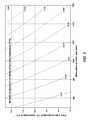
- FIG. 2is a simulation contour plot of wafer temperature sensitivity to face plate temperature and wafer-to-bake plate gap according to an embodiment of the present invention
- FIG. 3is an alternative simulation contour plot of wafer temperature sensitivity to face plate temperature and wafer-to-bake plate gap according to another embodiment of the present invention
- FIG. 4is a simplified flow chart illustrating a method of performing wafer temperature control according to an embodiment of the present invention
- FIG. 5is a plan view of a multi-zone bake plate having six different electrically independently heating zones according to an embodiment of the present invention.
- FIG. 6is a simplified architecture of a track lithography tool according to an embodiment of the present invention.
- embodiments of the present inventionpertain to a method and system for providing temperature control of a substrate disposed between a bake plate and an opposing face plate in a thermal module of a track lithography tool.
- certain embodiments of the present inventionhave been applied to maintain a substantially constant wafer temperature in a bake chamber of a track lithography tool by adjusting the bake plate temperature to compensate for changes in the face plate temperature, other embodiments of the present invention are not limited by this particular application.
- FIG. 1is a simplified cross sectional view of a bake chamber according to an embodiment of the invention.
- bake chamber 100has at least two separate isothermal elements: a face plate 110 and a bake plate 120 , each of which is manufactured from a material exhibiting high heat conductivity, such as aluminum or other appropriate material.
- Each plate 110 or 120has one or more heating elements, for example, resistive heating elements, embedded within the plate or otherwise in thermal communication with the plate.
- Bake chamber 100also includes a top side plate 112 and a bottom cup 122 , each coupled to the face plate 110 and bake plate 120 , respectively.
- bake chamber 100further includes top and bottom heat shields 116 and 126 , respectively.
- each of the heat shields 116 or 126are made from aluminum.
- the upper surface 121 of bake plate 120includes a plurality of proximity pins 125 configured to support a wafer loaded onto the proximity pins.
- Each proximity pins 125has a calibrated height above the upper surface 121 so that a substantially flat bottom surface of a loaded wafer is supported on the proximity pins with a predetermined distance between the bottom surface of the wafer and the upper surface 121 of the bake plate 120 .
- bake plate 120includes a plurality of vacuum ports (not shown in FIG. 1 ), which are operatively coupled to the bake plate to form a vacuum chuck configured to secure the wafer to the bake plate 120 .
- bake plate 120is operatively coupled to a motorized lift 22 so that the bake plate 120 can be raised from a wafer loading/receiving position to a baking position.
- the wafers or substratesare heated on bake plate 120 after the bake plate is raised to the baking position 11 (shown as a dashed line in FIG. 1 ) within a clam shell enclosure that contains the face plate 110 surrounded by the top side plate 112 .
- the bottom cup 122encircles a bottom portion of top side plate 112 forming the clam shell arrangement, which helps confine heat generated by bake plate 120 within an inner cavity formed by the bake plate and the enclosure.
- the face plate 110is positioned just above and opposing a top surface of the wafer supported on bake plate 120 .
- face plate 110includes a plurality of holes or channels 110 a that allow gases and contaminants baked off the wafer surface during baking processes to drift through face plate 110 and into a radially inward gas passageway that is provided as an inner structure (not shown) of the face plate 110 .
- Gas that flows in a radially inward direction through the gas passagewayis initially introduced into bake chamber 100 by a gas inlet line (not shown) at an annular gas manifold (not shown) that encircles the outer portion of top part of the face plate assembly.
- the gas manifoldincludes numerous small gas inlets that allow gas to flow from the manifold into the inner structure (not shown) of the face plate 110 .
- the gasflows radially inward towards the center of the bake station through a diffusion plate 114 that includes a plurality of gas outlet holes. After flowing through diffusion plate 114 , gas exits bake chamber 100 through gas outlet line 118 .
- gas outlet line 118gas outlet line 118 .
- the inward and outward radial flowsmay be reversed as appropriate to the particular application.
- the bake plate temperaturecan be accurately controlled via the embedded heating element provided in the bake plate in combination with control of the bake plate to wafer gap via the calibrated height of the proximity pins.
- Other conditions effecting the wafer temperatureincluding the face plate temperature and emissivity, gas thermal conductivity (once the flow rate and pressure are controlled), and the wafer to the face plate gap can be controlled in a repeatable manner during operation. Therefore in the bake chamber system configuration provided in accordance with embodiments of the present invention, the temperature of the wafer on the bake plate can, in principle, reach a steady state that is fully controllable once the appropriate conditions are known and repeatable. In practice, certain conditions tend to drift or change over time. For example, the face plate temperature is typically ignored in computations related to determining the bake plate temperature used to achieve the desired wafer temperature under the steady state condition. Such computations may lead to offsets in setting the bake plate temperature and errors in providing the desired wafer temperature.
- FIG. 2is a simulation contour plot of wafer temperature sensitivity to face plate temperature and wafer-to-bake plate gap according to an embodiment of the present invention.
- This diagramis merely an example, which should not unduly limit the scope of the claims herein.
- the simulation results in FIG. 2is based on the bake chamber 100 and associated system configuration shown in FIG. 1 .
- changes in the face plate temperaturewill affect the steady state wafer temperature. For example, assuming a 100 ⁇ m gap distance between the bake plate (which is at a set point temperature) and the wafer, if the face plate temperature drifts from about 85° C.
- Embodiments of the present inventionprovide for temperature compensation methods and systems useful in correcting this exemplary 0.2° C. error, thereby maintaining the wafer temperature at the desired steady state temperature.
- Embodiments of the present inventionprovide a method of providing substantially steady state wafer temperature control by accurately monitoring the face plate temperature and then determining and adjusting the bake plate temperature based on the measured plate temperature. Thus, face plate temperature drift is correctly compensated for during thermal processes by embodiments of the present invention. Further details of the method and related system setup will be described throughout this specification and more particularly below.
- the bake plate temperaturecan be controlled by receiving a temperature control signal from a controller 130 .
- controller 130can deliver the temperature control signal through a port 44 to the bake plate 120 .
- the temperature control signalis directed to the one or more heating elements 124 embedded within the bake plate 120 .
- the one or more heating elements 124are then able to adjust the power settings to increase or decrease the bake plate temperature so that the bake plate temperature becomes equal to a set point temperature, which may be predetermined prior to baking the wafer.
- a desired steady state temperaturemay be provided in advance of baking processes and may be modified during baking as appropriate to the particular application.
- each sensor 113contains a thermal measurement device such as a thermocouple or a resistance temperature detector (RTD).
- RTDresistance temperature detector
- Sensor 113is configured to sense a temperature at a local region of the face plate 110 and to collect temperature data either periodically or aperiodically.
- the controller 130is configured to receive sensor data from the plurality of sensors 113 .
- the sensor data measured at the sensors 113is transmitted from another port 33 coupled to the plurality of temperature sensors 113 to the controller 130 .
- wired connectionsare provided to transmit the data from the port 33 to the controller.
- Each sensor data valuerepresent a measured temperature of a corresponding region on the face plate.
- the controller 130is capable of processing the received sensor data, for example, making comparisons with one or more predetermined temperature values stored therein, determining a difference between the measured face plate temperature and the predetermined temperature value, and modifying the temperature control signal (provided to the bake plate) based on the determined temperature difference.
- the controller 130is able to refresh the temperature control signal every time period of t c .
- the modified temperature control signalcan then be delivered to the bake plate 120 through the port 44 at a similar period, that is, the time period of t c .
- the bake plate temperaturecan be adjusted from a first temperature at a first time to a second temperature at a second time, the first and second times being separated by the period t c .
- embodiments of the present inventionprovide for temperature compensation for the face plate temperature drift during bake processes.
- the systemoperates on a periodic basis (e.g., time period of t c ), although this is not required by the present invention.
- the periodmay be adjusted to longer or shorter times as appropriate to the particular application.
- the sensor response timeis about 50 seconds. In another embodiment, the sensor response time is about 20 seconds. In yet another embodiment, the sensor response time is preferably no greater than 10 seconds.
- the sensor response timeis preferably no greater than 10 seconds.
- FIG. 3is an alternative simulation contour plot of wafer temperature sensitivity to face plate temperature and wafer-to-bake plate gap according to another embodiment of the present invention.
- This diagramis merely an example, which should not unduly limit the scope of the claims herein.
- the simulation results in FIG. 3is based on the bake chamber 100 and associated system configuration shown in FIG. 1 .
- the wafer temperature sensitivity to face plate temperatureis illustrated as wafer temperature change per degree change of the face plate temperature at a fixed bake plate temperature. For example, assuming a 100 ⁇ m gap distance between the bake plate (which is set at a first temperature) and the wafer, if the face plate temperature changes from 101° C. to 100° C.
- the wafer temperaturewill increase by 0.035° C. Since the baking process is preferably performed in a steady state with all other conditions set in a repeatable manner, the change of wafer temperature as a result of the face plate temperature change can be corrected via a bake plate temperature compensation based on FIG. 3 .
- the bake plate temperaturewould need to be increased from the first temperature by 0.035° C. to a second temperature.
- the corrected temperature of the bake plateshould be equal to the first temperature plus 0.035° C.
- the compensation usedcan be determined using a pre-programmed algorithm in the controller and executed through one or more temperature control signal directed to the bake plate.
- the emissivity of the face plateaffects the radiation transfer to and from the face plate
- the emissivityaffects the face plate temperature drift.
- embodiments of the present inventionmaintain the emissivity of the face plate at a substantially constant value.
- the simulation results presented in FIG. 2 and FIG. 3utilize an emissivity value of 0.7 for the face plate.
- radicals or organic moleculesmay be vaporized from the substrate surface. Although most of these vapors are removed from the bake chamber by the central inward gas flow, some may deposit on the face plate surface. These organic depositions tend to increase the emissivity of the face plate.
- the face plate 110is made from aluminum or other suitable materials and is coated with one or more high emissivity materials having an emissivity greater than 0.95 in the infrared frequency range.
- possible coating materialsinclude PFA, polyimide, photoresist, and the like.
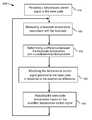
- FIG. 4is a simplified flow chart illustrating a method of performing wafer temperature control according to an embodiment of the present invention.
- This diagramis merely an example, which should not unduly limit the scope of the claims herein.
- the method 400 illustrated in FIG. 4may be performed after a wafer has been loaded on a bake plate, which is then raised to a baking position opposing a face plate in a thermal enclosure of the bake chamber.
- the method 400includes providing a temperature control signal to the bake plate ( 410 ) and measuring a face plate temperature associated with the face plate ( 420 ). Additionally, the method includes determining a difference between the face plate temperature and a predetermined temperature ( 430 ).
- the methodincludes modifying the temperature control signal provided to the bake plate in response to the determined difference ( 440 ). Furthermore, the method may include adjusting the bake plate temperature based on the modified temperature control signal to maintain a wafer temperature at a steady state (or a desired process temperature) ( 450 ).
- a controller coupled to the bake chamberis configured to provide one or more temperature control signals to the bake plate.
- the controllercan be disposed outside the bake chamber.
- the controlleris able to send one or temperature control signals through a communication port into a receiving unit that is coupled to one or more corresponding heating elements embedded in the bake plate.
- the temperature of the corresponding one or more heating elementsis modified, thereby controlling the wafer temperature.
- the communication portis coupled to heating elements that are located at multiple separate zones in the bake plate.
- the communication portmay be able to transmit or receive a wireless signal.
- the controllermay include control circuitry built into the bake chamber and configured to receive sensor data from a plurality of temperature sensors disposed on the face plate.
- the plurality of temperature sensorsare able to perform temperature measurements at various regions on the face plate.
- Each sensoris configured, for a specified response time t c , to sense a local temperature, generate temperature data, sent the temperature data to the controller, then repeat the process.
- the control circuitrycan compute the difference between the current measured temperature value and a predetermined temperature value depending on particular thermal process and baking chamber setup conditions (step 430 ). In one embodiment, step 430 periodically repeats with a time period of t c .
- step 430may include multiple computations performed in parallel. Such parallel processing may be performed either in a mutually independent manner or in an inter-related manner depending on particular process requirements.
- one or more temperature control signalsmay be processed or modified by the controller at step 440 .
- a pre-loaded wafer temperature sensitivity to the face plate temperaturehas been established either through simulation or empirical data collected during processing experiments for a given bake chamber configuration. For example, plots like that shown in FIG. 2 or FIG. 3 can be obtained and programmed into the control circuitry for proper modification of the one or more temperature control signals that are provided to the bake plate.
- plots like that shown in FIG. 2 or FIG. 3can be obtained and programmed into the control circuitry for proper modification of the one or more temperature control signals that are provided to the bake plate.
- the temperature sensitivity to the face plate temperatureis a negative response indicator of the temperature compensation provided to the bake plate temperature in order to maintain a steady state wafer temperature.
- the bake plate temperaturewill be adjusted by the modified control signal.
- the modified control signalis derived from a negative response indicator associated with the temperature sensitivity to the face plate temperature.
- the control signalwould be modified in a negative way by the control circuitry.
- the modified corresponding control signalshould lead to an appropriate increase of bake plate temperature to provide the desired temperature compensation.
- the modified control signal based on the negative response indicatorwill provide bake plate control signals that will result in a decrease in bake plate temperature, thereby properly achieving the desired steady state temperature control for the wafer.
- FIG. 4provides a particular method of controlling wafer temperature during thermal processing in a semiconductor chamber according to an embodiment of the present invention.
- Other sequences of stepsmay also be performed according to alternative embodiments.
- same sequence of stepsmay be repeated loops that are cycled in a period of time t c , where t c is associated with a temperature sensor's sensing response time.
- Embodiments of the present inventionmay perform the steps outlined above in a different order.
- the individual steps illustrated in FIG. 4may include multiple sub-steps that may be performed in various sequences as appropriate to the individual step.
- additional stepsmay be added or removed depending on the particular applications.
- One of ordinary skill in the artwould recognize many variations, modifications, and alternatives.
- the bake platemay include multiple zones in which separate heating elements are embedded and independently coupled to the controller for receiving corresponding temperature control signals.
- the temperature at each zonecan be independently controlled.
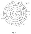
- FIG. 5is a plan view of a multi-zone bake plate having six different electrically independently heating zones according to an embodiment of the present invention.
- the bake plate 50includes two or more insulating layers with a kapton layer sandwiched between the insulating layers.
- the bake plate 10is the bake plate 120 utilized in the bake chamber 100 illustrated in FIG. 1 . As shown in FIG.
- bake plate 50includes six independent heater zones 12 1 - 12 6 along with a corresponding number of second temperature sensors 14 1 - 14 6 , one for each of the heater zones 12 1 - 12 6 .
- each of the heater zones 12 1 - 12 6respectively is opposing one region on the face plate where a corresponding first temperature sensor may be disposed to detect the temperature at the corresponding region of the face plate.
- a controllercan receive sensor data, one for each region on the face plate from a corresponding first temperature sensor corresponding to multiple regions of the face plate respectively opposing the heater zones 12 1 - 12 6 .
- RTDsresistance temperature detectors
- a controllercan receive sensor data, one for each region on the face plate from a corresponding first temperature sensor corresponding to multiple regions of the face plate respectively opposing the heater zones 12 1 - 12 6 .
- the controllercan provide a modified temperature control signal to a corresponding heating element of one heater zone among the heater zones 12 1 - 12 6 .
- Metal traces formed into a patterned wiring layer for each heating elementare then used to resistively heat the various heater zones 12 1 - 12 6 .
- the bake plate 50has multiple zone temperatures independently controlled in particular heater zones that separately compensate the temperature drift at corresponding regions of the face plate.
- the mapping from face plate regions to bake plate zonesmay be a function depending on additional face plate regions not opposing the bake plate zone.
- One of ordinary skill in the artwould recognize many variations, modifications, and alternatives. Additional description of multi-zone heater plates is provided in U.S. patent application Ser. No. 11/483,832, filed on Jul. 7, 2006, commonly assigned and hereby incorporated by reference for all purposes.
- FIG. 6is a simplified architecture of a track lithography tool according to an embodiment of the present invention.
- track lithography 200contains a front end module 210 (sometimes referred to as a factory interface) 210 , a central module 212 , and a rear module 214 (sometimes referred to as a scanner interface).
- Front end module 210generally contains one or more pod assemblies or FOUPS (e.g., items 216 A-D), a front end robot 218 , and front end processing racks 220 A, 220 B.
- the one or more pod assemblies 216 A-Dare generally adapted to accept one or more cassettes 230 that may contain one or more substrates “W”, or wafers, that are to be processed in track lithography tool 200 .
- Central module 212generally contains a first central processing rack 222 A, a second central processing rack 222 B, and a central robot 224 .
- Rear module 214generally contains first and second rear processing racks 226 A, 226 B and a back end robot 228 .
- Front end robot 218is adapted to access processing modules in front end processing racks 220 A, 220 B;
- central robot 224is adapted to access processing modules in front end processing racks 220 A, 220 B, first central processing rack 222 A, second central processing rack 222 B and/or rear processing racks 226 A, 226 B;
- back end robot 228is adapted to access processing modules in the rear processing racks 226 A, 226 B and in some cases exchange substrates with a stepper/scanner 5 .
- the stepper/scanner 5which may be purchased from Canon USA, Inc. of San Jose, Calif., Nikon Precision Inc. of Belmont, Calif., or ASML US, Inc. of Tempe Ariz., is a lithographic projection apparatus used, for example, in the manufacture of integrated circuits (ICs).
- the scanner/stepper tool 5exposes a photosensitive material (resist), deposited on the substrate in the cluster tool, to some form of electromagnetic radiation to generate a circuit pattern corresponding to an individual layer of the integrated circuit (IC) device to be formed on the substrate surface.
- a photosensitive materialresist
- Each of the processing racks 220 A, 220 B; 222 A, 222 B and 226 A, 226 Bcontain multiple processing modules in a vertically stacked arrangement. That is, each of the processing racks may contain multiple stacked integrated thermal units 10 , multiple stacked coater modules 232 , multiple stacked coater/developer modules with shared dispense 234 or other modules that are adapted to perform the various processing steps required of a track photolithography tool.
- coater modules 232may deposit a bottom antireflective coating (BARC); coater/developer modules 234 may be used to deposit and/or develop photoresist layers and integrated thermal units 10 may perform bake and chill operations associated with hardening BARC and/or photoresist layers.
- BARCbottom antireflective coating
- a system controller 240is used to control all of the components and processes performed in the cluster tool 200 .
- the controller 240is generally adapted to communicate with the stepper/scanner 5 , monitor and control aspects of the processes performed in the cluster tool 200 , and is adapted to control all aspects of the complete substrate processing sequence.
- controller 240works in conjunction with other controllers, such as controllers 46 A- 46 D, which control hot plate 20 and chill plate 30 of integrated thermal unit 10 , to control certain aspects of the processing sequence.
- the controller 240which is typically a microprocessor-based controller, is configured to receive inputs from a user and/or various sensors in one of the processing chambers and appropriately control the processing chamber components in accordance with the various inputs and software instructions retained in the controller's memory.
- the controller 240generally contains memory and a CPU (not shown) which are utilized by the controller to retain various programs, process the programs, and execute the programs when necessary.
- the memory(not shown) is connected to the CPU, and may be one or more of a readily available memory, such as random access memory (RAM), read only memory (ROM), floppy disk, hard disk, or any other form of digital storage, local or remote.
- Software instructions and datacan be coded and stored within the memory for instructing the CPU.
- the support circuitsare also connected to the CPU for supporting the processor in a conventional manner.
- the support circuitsmay include cache, power supplies, clock circuits, input/output circuitry, subsystems, and the like all well known in the art.
- a program (or computer instructions) readable by the controller 240determines which tasks are performable in the processing chamber(s).
- the programis software readable by the controller 240 and includes instructions to monitor and control the process based on defined rules and input data.
- embodiments of the inventionare not limited to use with a track lithography tool such as that depicted in FIG. 6 . Instead, embodiments of the invention may be used in any track lithography tool including the many different tool configurations described in U.S. application Ser. No. 11/112,281 entitled “Cluster Tool Architecture for Processing a Substrate” filed on Apr. 22, 2005, which is hereby incorporated by reference for all purposes and including configurations not described in the Ser. No. 11/112,281 application.
Landscapes
- Engineering & Computer Science (AREA)
- Physics & Mathematics (AREA)
- Condensed Matter Physics & Semiconductors (AREA)
- General Physics & Mathematics (AREA)
- Manufacturing & Machinery (AREA)
- Computer Hardware Design (AREA)
- Microelectronics & Electronic Packaging (AREA)
- Power Engineering (AREA)
- Mechanical Engineering (AREA)
- General Engineering & Computer Science (AREA)
- Exposure Of Semiconductors, Excluding Electron Or Ion Beam Exposure (AREA)
Abstract
Description
Claims (5)
Priority Applications (1)
| Application Number | Priority Date | Filing Date | Title |
|---|---|---|---|
| US11/849,978US7831135B2 (en) | 2007-09-04 | 2007-09-04 | Method and system for controlling bake plate temperature in a semiconductor processing chamber |
Applications Claiming Priority (1)
| Application Number | Priority Date | Filing Date | Title |
|---|---|---|---|
| US11/849,978US7831135B2 (en) | 2007-09-04 | 2007-09-04 | Method and system for controlling bake plate temperature in a semiconductor processing chamber |
Publications (2)
| Publication Number | Publication Date |
|---|---|
| US20090060480A1 US20090060480A1 (en) | 2009-03-05 |
| US7831135B2true US7831135B2 (en) | 2010-11-09 |
Family
ID=40407673
Family Applications (1)
| Application Number | Title | Priority Date | Filing Date |
|---|---|---|---|
| US11/849,978Active2028-08-24US7831135B2 (en) | 2007-09-04 | 2007-09-04 | Method and system for controlling bake plate temperature in a semiconductor processing chamber |
Country Status (1)
| Country | Link |
|---|---|
| US (1) | US7831135B2 (en) |
Families Citing this family (247)
| Publication number | Priority date | Publication date | Assignee | Title |
|---|---|---|---|---|
| US8282768B1 (en) | 2005-04-26 | 2012-10-09 | Novellus Systems, Inc. | Purging of porogen from UV cure chamber |
| US8137465B1 (en) | 2005-04-26 | 2012-03-20 | Novellus Systems, Inc. | Single-chamber sequential curing of semiconductor wafers |
| US20100270004A1 (en)* | 2005-05-12 | 2010-10-28 | Landess James D | Tailored profile pedestal for thermo-elastically stable cooling or heating of substrates |
| US7941039B1 (en) | 2005-07-18 | 2011-05-10 | Novellus Systems, Inc. | Pedestal heat transfer and temperature control |
| US7960297B1 (en) | 2006-12-07 | 2011-06-14 | Novellus Systems, Inc. | Load lock design for rapid wafer heating |
| JP5006122B2 (en) | 2007-06-29 | 2012-08-22 | 株式会社Sokudo | Substrate processing equipment |
| US8052419B1 (en)* | 2007-11-08 | 2011-11-08 | Novellus Systems, Inc. | Closed loop temperature heat up and control utilizing wafer-to-heater pedestal gap modulation |
| JP5128918B2 (en) | 2007-11-30 | 2013-01-23 | 株式会社Sokudo | Substrate processing equipment |
| JP5160204B2 (en)* | 2007-11-30 | 2013-03-13 | 株式会社Sokudo | Substrate processing equipment |
| JP5179170B2 (en) | 2007-12-28 | 2013-04-10 | 株式会社Sokudo | Substrate processing equipment |
| JP5001828B2 (en) | 2007-12-28 | 2012-08-15 | 株式会社Sokudo | Substrate processing equipment |
| US8033771B1 (en) | 2008-12-11 | 2011-10-11 | Novellus Systems, Inc. | Minimum contact area wafer clamping with gas flow for rapid wafer cooling |
| US8371567B2 (en) | 2011-04-13 | 2013-02-12 | Novellus Systems, Inc. | Pedestal covers |
| US20130023129A1 (en) | 2011-07-20 | 2013-01-24 | Asm America, Inc. | Pressure transmitter for a semiconductor processing environment |
| CN104040710B (en) | 2012-01-06 | 2017-11-28 | 诺发系统公司 | Adaptive heat-transferring method and system for uniformly transfer heat |
| US20160376700A1 (en) | 2013-02-01 | 2016-12-29 | Asm Ip Holding B.V. | System for treatment of deposition reactor |
| US10006717B2 (en)* | 2014-03-07 | 2018-06-26 | Taiwan Semiconductor Manufacturing Company, Ltd. | Adaptive baking system and method of using the same |
| US9790581B2 (en)* | 2014-06-25 | 2017-10-17 | Fm Industries, Inc. | Emissivity controlled coatings for semiconductor chamber components |
| US10941490B2 (en) | 2014-10-07 | 2021-03-09 | Asm Ip Holding B.V. | Multiple temperature range susceptor, assembly, reactor and system including the susceptor, and methods of using the same |
| US10276355B2 (en) | 2015-03-12 | 2019-04-30 | Asm Ip Holding B.V. | Multi-zone reactor, system including the reactor, and method of using the same |
| US11139308B2 (en) | 2015-12-29 | 2021-10-05 | Asm Ip Holding B.V. | Atomic layer deposition of III-V compounds to form V-NAND devices |
| US10529554B2 (en) | 2016-02-19 | 2020-01-07 | Asm Ip Holding B.V. | Method for forming silicon nitride film selectively on sidewalls or flat surfaces of trenches |
| US10343920B2 (en) | 2016-03-18 | 2019-07-09 | Asm Ip Holding B.V. | Aligned carbon nanotubes |
| US11453943B2 (en) | 2016-05-25 | 2022-09-27 | Asm Ip Holding B.V. | Method for forming carbon-containing silicon/metal oxide or nitride film by ALD using silicon precursor and hydrocarbon precursor |
| US10612137B2 (en) | 2016-07-08 | 2020-04-07 | Asm Ip Holdings B.V. | Organic reactants for atomic layer deposition |
| US9859151B1 (en) | 2016-07-08 | 2018-01-02 | Asm Ip Holding B.V. | Selective film deposition method to form air gaps |
| US9887082B1 (en) | 2016-07-28 | 2018-02-06 | Asm Ip Holding B.V. | Method and apparatus for filling a gap |
| US9812320B1 (en) | 2016-07-28 | 2017-11-07 | Asm Ip Holding B.V. | Method and apparatus for filling a gap |
| US10347547B2 (en) | 2016-08-09 | 2019-07-09 | Lam Research Corporation | Suppressing interfacial reactions by varying the wafer temperature throughout deposition |
| US11532757B2 (en) | 2016-10-27 | 2022-12-20 | Asm Ip Holding B.V. | Deposition of charge trapping layers |
| US10714350B2 (en) | 2016-11-01 | 2020-07-14 | ASM IP Holdings, B.V. | Methods for forming a transition metal niobium nitride film on a substrate by atomic layer deposition and related semiconductor device structures |
| KR102546317B1 (en) | 2016-11-15 | 2023-06-21 | 에이에스엠 아이피 홀딩 비.브이. | Gas supply unit and substrate processing apparatus including the same |
| US11447861B2 (en) | 2016-12-15 | 2022-09-20 | Asm Ip Holding B.V. | Sequential infiltration synthesis apparatus and a method of forming a patterned structure |
| US11581186B2 (en) | 2016-12-15 | 2023-02-14 | Asm Ip Holding B.V. | Sequential infiltration synthesis apparatus |
| JP6789096B2 (en)* | 2016-12-22 | 2020-11-25 | 東京エレクトロン株式会社 | Heat treatment equipment, heat treatment method and computer storage medium |
| US11390950B2 (en) | 2017-01-10 | 2022-07-19 | Asm Ip Holding B.V. | Reactor system and method to reduce residue buildup during a film deposition process |
| US10468261B2 (en) | 2017-02-15 | 2019-11-05 | Asm Ip Holding B.V. | Methods for forming a metallic film on a substrate by cyclical deposition and related semiconductor device structures |
| US10770286B2 (en) | 2017-05-08 | 2020-09-08 | Asm Ip Holdings B.V. | Methods for selectively forming a silicon nitride film on a substrate and related semiconductor device structures |
| US12040200B2 (en) | 2017-06-20 | 2024-07-16 | Asm Ip Holding B.V. | Semiconductor processing apparatus and methods for calibrating a semiconductor processing apparatus |
| US10361099B2 (en)* | 2017-06-23 | 2019-07-23 | Applied Materials, Inc. | Systems and methods of gap calibration via direct component contact in electronic device manufacturing systems |
| US11306395B2 (en) | 2017-06-28 | 2022-04-19 | Asm Ip Holding B.V. | Methods for depositing a transition metal nitride film on a substrate by atomic layer deposition and related deposition apparatus |
| KR20190009245A (en) | 2017-07-18 | 2019-01-28 | 에이에스엠 아이피 홀딩 비.브이. | Methods for forming a semiconductor device structure and related semiconductor device structures |
| US11374112B2 (en) | 2017-07-19 | 2022-06-28 | Asm Ip Holding B.V. | Method for depositing a group IV semiconductor and related semiconductor device structures |
| US10590535B2 (en) | 2017-07-26 | 2020-03-17 | Asm Ip Holdings B.V. | Chemical treatment, deposition and/or infiltration apparatus and method for using the same |
| TWI815813B (en) | 2017-08-04 | 2023-09-21 | 荷蘭商Asm智慧財產控股公司 | Showerhead assembly for distributing a gas within a reaction chamber |
| US10770336B2 (en) | 2017-08-08 | 2020-09-08 | Asm Ip Holding B.V. | Substrate lift mechanism and reactor including same |
| US10692741B2 (en) | 2017-08-08 | 2020-06-23 | Asm Ip Holdings B.V. | Radiation shield |
| US11769682B2 (en) | 2017-08-09 | 2023-09-26 | Asm Ip Holding B.V. | Storage apparatus for storing cassettes for substrates and processing apparatus equipped therewith |
| US11830730B2 (en) | 2017-08-29 | 2023-11-28 | Asm Ip Holding B.V. | Layer forming method and apparatus |
| US11295980B2 (en) | 2017-08-30 | 2022-04-05 | Asm Ip Holding B.V. | Methods for depositing a molybdenum metal film over a dielectric surface of a substrate by a cyclical deposition process and related semiconductor device structures |
| US10658205B2 (en) | 2017-09-28 | 2020-05-19 | Asm Ip Holdings B.V. | Chemical dispensing apparatus and methods for dispensing a chemical to a reaction chamber |
| US10403504B2 (en) | 2017-10-05 | 2019-09-03 | Asm Ip Holding B.V. | Method for selectively depositing a metallic film on a substrate |
| US10923344B2 (en) | 2017-10-30 | 2021-02-16 | Asm Ip Holding B.V. | Methods for forming a semiconductor structure and related semiconductor structures |
| CN111344522B (en) | 2017-11-27 | 2022-04-12 | 阿斯莫Ip控股公司 | Including clean mini-environment device |
| WO2019103613A1 (en) | 2017-11-27 | 2019-05-31 | Asm Ip Holding B.V. | A storage device for storing wafer cassettes for use with a batch furnace |
| US10872771B2 (en) | 2018-01-16 | 2020-12-22 | Asm Ip Holding B. V. | Method for depositing a material film on a substrate within a reaction chamber by a cyclical deposition process and related device structures |
| TWI799494B (en) | 2018-01-19 | 2023-04-21 | 荷蘭商Asm 智慧財產控股公司 | Deposition method |
| KR102695659B1 (en) | 2018-01-19 | 2024-08-14 | 에이에스엠 아이피 홀딩 비.브이. | Method for depositing a gap filling layer by plasma assisted deposition |
| US11081345B2 (en) | 2018-02-06 | 2021-08-03 | Asm Ip Holding B.V. | Method of post-deposition treatment for silicon oxide film |
| WO2019158960A1 (en) | 2018-02-14 | 2019-08-22 | Asm Ip Holding B.V. | A method for depositing a ruthenium-containing film on a substrate by a cyclical deposition process |
| US10896820B2 (en) | 2018-02-14 | 2021-01-19 | Asm Ip Holding B.V. | Method for depositing a ruthenium-containing film on a substrate by a cyclical deposition process |
| US10731249B2 (en) | 2018-02-15 | 2020-08-04 | Asm Ip Holding B.V. | Method of forming a transition metal containing film on a substrate by a cyclical deposition process, a method for supplying a transition metal halide compound to a reaction chamber, and related vapor deposition apparatus |
| KR102636427B1 (en) | 2018-02-20 | 2024-02-13 | 에이에스엠 아이피 홀딩 비.브이. | Substrate processing method and apparatus |
| US10975470B2 (en) | 2018-02-23 | 2021-04-13 | Asm Ip Holding B.V. | Apparatus for detecting or monitoring for a chemical precursor in a high temperature environment |
| US11473195B2 (en) | 2018-03-01 | 2022-10-18 | Asm Ip Holding B.V. | Semiconductor processing apparatus and a method for processing a substrate |
| KR102646467B1 (en) | 2018-03-27 | 2024-03-11 | 에이에스엠 아이피 홀딩 비.브이. | Method of forming an electrode on a substrate and a semiconductor device structure including an electrode |
| KR102600229B1 (en) | 2018-04-09 | 2023-11-10 | 에이에스엠 아이피 홀딩 비.브이. | Substrate supporting device, substrate processing apparatus including the same and substrate processing method |
| US12025484B2 (en) | 2018-05-08 | 2024-07-02 | Asm Ip Holding B.V. | Thin film forming method |
| US12272527B2 (en) | 2018-05-09 | 2025-04-08 | Asm Ip Holding B.V. | Apparatus for use with hydrogen radicals and method of using same |
| KR102596988B1 (en) | 2018-05-28 | 2023-10-31 | 에이에스엠 아이피 홀딩 비.브이. | Method of processing a substrate and a device manufactured by the same |
| US11718913B2 (en) | 2018-06-04 | 2023-08-08 | Asm Ip Holding B.V. | Gas distribution system and reactor system including same |
| US10797133B2 (en) | 2018-06-21 | 2020-10-06 | Asm Ip Holding B.V. | Method for depositing a phosphorus doped silicon arsenide film and related semiconductor device structures |
| KR102568797B1 (en) | 2018-06-21 | 2023-08-21 | 에이에스엠 아이피 홀딩 비.브이. | Substrate processing system |
| TWI873894B (en) | 2018-06-27 | 2025-02-21 | 荷蘭商Asm Ip私人控股有限公司 | Cyclic deposition methods for forming metal-containing material and films and structures including the metal-containing material |
| KR102854019B1 (en) | 2018-06-27 | 2025-09-02 | 에이에스엠 아이피 홀딩 비.브이. | Periodic deposition method for forming a metal-containing material and films and structures comprising the metal-containing material |
| US10755922B2 (en) | 2018-07-03 | 2020-08-25 | Asm Ip Holding B.V. | Method for depositing silicon-free carbon-containing film as gap-fill layer by pulse plasma-assisted deposition |
| US10388513B1 (en) | 2018-07-03 | 2019-08-20 | Asm Ip Holding B.V. | Method for depositing silicon-free carbon-containing film as gap-fill layer by pulse plasma-assisted deposition |
| US11430674B2 (en) | 2018-08-22 | 2022-08-30 | Asm Ip Holding B.V. | Sensor array, apparatus for dispensing a vapor phase reactant to a reaction chamber and related methods |
| US11024523B2 (en) | 2018-09-11 | 2021-06-01 | Asm Ip Holding B.V. | Substrate processing apparatus and method |
| KR102707956B1 (en) | 2018-09-11 | 2024-09-19 | 에이에스엠 아이피 홀딩 비.브이. | Method for deposition of a thin film |
| CN110970344B (en) | 2018-10-01 | 2024-10-25 | Asmip控股有限公司 | Substrate holding apparatus, system comprising the same and method of using the same |
| KR102592699B1 (en) | 2018-10-08 | 2023-10-23 | 에이에스엠 아이피 홀딩 비.브이. | Substrate support unit and apparatuses for depositing thin film and processing the substrate including the same |
| KR102546322B1 (en) | 2018-10-19 | 2023-06-21 | 에이에스엠 아이피 홀딩 비.브이. | Substrate processing apparatus and substrate processing method |
| US12378665B2 (en) | 2018-10-26 | 2025-08-05 | Asm Ip Holding B.V. | High temperature coatings for a preclean and etch apparatus and related methods |
| US11087997B2 (en) | 2018-10-31 | 2021-08-10 | Asm Ip Holding B.V. | Substrate processing apparatus for processing substrates |
| KR102748291B1 (en) | 2018-11-02 | 2024-12-31 | 에이에스엠 아이피 홀딩 비.브이. | Substrate support unit and substrate processing apparatus including the same |
| US11572620B2 (en) | 2018-11-06 | 2023-02-07 | Asm Ip Holding B.V. | Methods for selectively depositing an amorphous silicon film on a substrate |
| US10818758B2 (en) | 2018-11-16 | 2020-10-27 | Asm Ip Holding B.V. | Methods for forming a metal silicate film on a substrate in a reaction chamber and related semiconductor device structures |
| US12040199B2 (en) | 2018-11-28 | 2024-07-16 | Asm Ip Holding B.V. | Substrate processing apparatus for processing substrates |
| KR102636428B1 (en) | 2018-12-04 | 2024-02-13 | 에이에스엠 아이피 홀딩 비.브이. | A method for cleaning a substrate processing apparatus |
| US11158513B2 (en) | 2018-12-13 | 2021-10-26 | Asm Ip Holding B.V. | Methods for forming a rhenium-containing film on a substrate by a cyclical deposition process and related semiconductor device structures |
| TWI874340B (en) | 2018-12-14 | 2025-03-01 | 荷蘭商Asm Ip私人控股有限公司 | Method of forming device structure, structure formed by the method and system for performing the method |
| TWI866480B (en) | 2019-01-17 | 2024-12-11 | 荷蘭商Asm Ip 私人控股有限公司 | Methods of forming a transition metal containing film on a substrate by a cyclical deposition process |
| TWI845607B (en) | 2019-02-20 | 2024-06-21 | 荷蘭商Asm Ip私人控股有限公司 | Cyclical deposition method and apparatus for filling a recess formed within a substrate surface |
| TWI873122B (en) | 2019-02-20 | 2025-02-21 | 荷蘭商Asm Ip私人控股有限公司 | Method of filling a recess formed within a surface of a substrate, semiconductor structure formed according to the method, and semiconductor processing apparatus |
| TWI838458B (en) | 2019-02-20 | 2024-04-11 | 荷蘭商Asm Ip私人控股有限公司 | Apparatus and methods for plug fill deposition in 3-d nand applications |
| TWI842826B (en) | 2019-02-22 | 2024-05-21 | 荷蘭商Asm Ip私人控股有限公司 | Substrate processing apparatus and method for processing substrate |
| US11742198B2 (en) | 2019-03-08 | 2023-08-29 | Asm Ip Holding B.V. | Structure including SiOCN layer and method of forming same |
| KR102858005B1 (en) | 2019-03-08 | 2025-09-09 | 에이에스엠 아이피 홀딩 비.브이. | Method for Selective Deposition of Silicon Nitride Layer and Structure Including Selectively-Deposited Silicon Nitride Layer |
| JP2020167398A (en) | 2019-03-28 | 2020-10-08 | エーエスエム・アイピー・ホールディング・ベー・フェー | Door openers and substrate processing equipment provided with door openers |
| KR102809999B1 (en) | 2019-04-01 | 2025-05-19 | 에이에스엠 아이피 홀딩 비.브이. | Method of manufacturing semiconductor device |
| KR20200123380A (en) | 2019-04-19 | 2020-10-29 | 에이에스엠 아이피 홀딩 비.브이. | Layer forming method and apparatus |
| KR20200125453A (en) | 2019-04-24 | 2020-11-04 | 에이에스엠 아이피 홀딩 비.브이. | Gas-phase reactor system and method of using same |
| KR20200130121A (en) | 2019-05-07 | 2020-11-18 | 에이에스엠 아이피 홀딩 비.브이. | Chemical source vessel with dip tube |
| KR20200130652A (en) | 2019-05-10 | 2020-11-19 | 에이에스엠 아이피 홀딩 비.브이. | Method of depositing material onto a surface and structure formed according to the method |
| JP7612342B2 (en) | 2019-05-16 | 2025-01-14 | エーエスエム・アイピー・ホールディング・ベー・フェー | Wafer boat handling apparatus, vertical batch furnace and method |
| JP7598201B2 (en) | 2019-05-16 | 2024-12-11 | エーエスエム・アイピー・ホールディング・ベー・フェー | Wafer boat handling apparatus, vertical batch furnace and method |
| USD947913S1 (en) | 2019-05-17 | 2022-04-05 | Asm Ip Holding B.V. | Susceptor shaft |
| USD975665S1 (en) | 2019-05-17 | 2023-01-17 | Asm Ip Holding B.V. | Susceptor shaft |
| KR102280033B1 (en)* | 2019-05-29 | 2021-07-21 | 세메스 주식회사 | Apparatus for treating substrate and method for treating apparatus |
| KR20200141002A (en) | 2019-06-06 | 2020-12-17 | 에이에스엠 아이피 홀딩 비.브이. | Method of using a gas-phase reactor system including analyzing exhausted gas |
| KR20200141931A (en) | 2019-06-10 | 2020-12-21 | 에이에스엠 아이피 홀딩 비.브이. | Method for cleaning quartz epitaxial chambers |
| KR20200143254A (en) | 2019-06-11 | 2020-12-23 | 에이에스엠 아이피 홀딩 비.브이. | Method of forming an electronic structure using an reforming gas, system for performing the method, and structure formed using the method |
| KR20210005515A (en) | 2019-07-03 | 2021-01-14 | 에이에스엠 아이피 홀딩 비.브이. | Temperature control assembly for substrate processing apparatus and method of using same |
| JP7499079B2 (en) | 2019-07-09 | 2024-06-13 | エーエスエム・アイピー・ホールディング・ベー・フェー | Plasma device using coaxial waveguide and substrate processing method |
| CN112216646A (en) | 2019-07-10 | 2021-01-12 | Asm Ip私人控股有限公司 | Substrate supporting assembly and substrate processing device comprising same |
| KR20210010307A (en) | 2019-07-16 | 2021-01-27 | 에이에스엠 아이피 홀딩 비.브이. | Substrate processing apparatus |
| KR102860110B1 (en) | 2019-07-17 | 2025-09-16 | 에이에스엠 아이피 홀딩 비.브이. | Methods of forming silicon germanium structures |
| KR20210010816A (en) | 2019-07-17 | 2021-01-28 | 에이에스엠 아이피 홀딩 비.브이. | Radical assist ignition plasma system and method |
| US11643724B2 (en) | 2019-07-18 | 2023-05-09 | Asm Ip Holding B.V. | Method of forming structures using a neutral beam |
| KR20210010817A (en) | 2019-07-19 | 2021-01-28 | 에이에스엠 아이피 홀딩 비.브이. | Method of Forming Topology-Controlled Amorphous Carbon Polymer Film |
| TWI851767B (en) | 2019-07-29 | 2024-08-11 | 荷蘭商Asm Ip私人控股有限公司 | Methods for selective deposition utilizing n-type dopants and/or alternative dopants to achieve high dopant incorporation |
| CN112309900A (en) | 2019-07-30 | 2021-02-02 | Asm Ip私人控股有限公司 | Substrate processing apparatus |
| CN112309899A (en) | 2019-07-30 | 2021-02-02 | Asm Ip私人控股有限公司 | Substrate processing apparatus |
| US12169361B2 (en) | 2019-07-30 | 2024-12-17 | Asm Ip Holding B.V. | Substrate processing apparatus and method |
| US11587814B2 (en) | 2019-07-31 | 2023-02-21 | Asm Ip Holding B.V. | Vertical batch furnace assembly |
| US11227782B2 (en) | 2019-07-31 | 2022-01-18 | Asm Ip Holding B.V. | Vertical batch furnace assembly |
| US11587815B2 (en) | 2019-07-31 | 2023-02-21 | Asm Ip Holding B.V. | Vertical batch furnace assembly |
| CN112323048B (en) | 2019-08-05 | 2024-02-09 | Asm Ip私人控股有限公司 | Liquid level sensor for chemical source container |
| CN112342526A (en) | 2019-08-09 | 2021-02-09 | Asm Ip私人控股有限公司 | Heater assembly including cooling device and method of using same |
| USD965044S1 (en) | 2019-08-19 | 2022-09-27 | Asm Ip Holding B.V. | Susceptor shaft |
| USD965524S1 (en) | 2019-08-19 | 2022-10-04 | Asm Ip Holding B.V. | Susceptor support |
| JP2021031769A (en) | 2019-08-21 | 2021-03-01 | エーエスエム アイピー ホールディング ビー.ブイ. | Production apparatus of mixed gas of film deposition raw material and film deposition apparatus |
| KR20210024423A (en) | 2019-08-22 | 2021-03-05 | 에이에스엠 아이피 홀딩 비.브이. | Method for forming a structure with a hole |
| USD979506S1 (en) | 2019-08-22 | 2023-02-28 | Asm Ip Holding B.V. | Insulator |
| KR20210024420A (en) | 2019-08-23 | 2021-03-05 | 에이에스엠 아이피 홀딩 비.브이. | Method for depositing silicon oxide film having improved quality by peald using bis(diethylamino)silane |
| US11286558B2 (en) | 2019-08-23 | 2022-03-29 | Asm Ip Holding B.V. | Methods for depositing a molybdenum nitride film on a surface of a substrate by a cyclical deposition process and related semiconductor device structures including a molybdenum nitride film |
| KR102806450B1 (en) | 2019-09-04 | 2025-05-12 | 에이에스엠 아이피 홀딩 비.브이. | Methods for selective deposition using a sacrificial capping layer |
| KR102733104B1 (en) | 2019-09-05 | 2024-11-22 | 에이에스엠 아이피 홀딩 비.브이. | Substrate processing apparatus |
| US11562901B2 (en) | 2019-09-25 | 2023-01-24 | Asm Ip Holding B.V. | Substrate processing method |
| CN112593212B (en) | 2019-10-02 | 2023-12-22 | Asm Ip私人控股有限公司 | Method for forming topologically selective silicon oxide film by cyclic plasma enhanced deposition process |
| TWI846953B (en) | 2019-10-08 | 2024-07-01 | 荷蘭商Asm Ip私人控股有限公司 | Substrate processing device |
| KR20210042810A (en) | 2019-10-08 | 2021-04-20 | 에이에스엠 아이피 홀딩 비.브이. | Reactor system including a gas distribution assembly for use with activated species and method of using same |
| TW202128273A (en) | 2019-10-08 | 2021-08-01 | 荷蘭商Asm Ip私人控股有限公司 | Gas injection system, reactor system, and method of depositing material on surface of substratewithin reaction chamber |
| TWI846966B (en) | 2019-10-10 | 2024-07-01 | 荷蘭商Asm Ip私人控股有限公司 | Method of forming a photoresist underlayer and structure including same |
| US12009241B2 (en) | 2019-10-14 | 2024-06-11 | Asm Ip Holding B.V. | Vertical batch furnace assembly with detector to detect cassette |
| TWI834919B (en) | 2019-10-16 | 2024-03-11 | 荷蘭商Asm Ip私人控股有限公司 | Method of topology-selective film formation of silicon oxide |
| US11637014B2 (en) | 2019-10-17 | 2023-04-25 | Asm Ip Holding B.V. | Methods for selective deposition of doped semiconductor material |
| KR102845724B1 (en) | 2019-10-21 | 2025-08-13 | 에이에스엠 아이피 홀딩 비.브이. | Apparatus and methods for selectively etching films |
| KR20210050453A (en) | 2019-10-25 | 2021-05-07 | 에이에스엠 아이피 홀딩 비.브이. | Methods for filling a gap feature on a substrate surface and related semiconductor structures |
| US11646205B2 (en) | 2019-10-29 | 2023-05-09 | Asm Ip Holding B.V. | Methods of selectively forming n-type doped material on a surface, systems for selectively forming n-type doped material, and structures formed using same |
| KR20210054983A (en) | 2019-11-05 | 2021-05-14 | 에이에스엠 아이피 홀딩 비.브이. | Structures with doped semiconductor layers and methods and systems for forming same |
| US11501968B2 (en) | 2019-11-15 | 2022-11-15 | Asm Ip Holding B.V. | Method for providing a semiconductor device with silicon filled gaps |
| KR102861314B1 (en) | 2019-11-20 | 2025-09-17 | 에이에스엠 아이피 홀딩 비.브이. | Method of depositing carbon-containing material on a surface of a substrate, structure formed using the method, and system for forming the structure |
| US11450529B2 (en) | 2019-11-26 | 2022-09-20 | Asm Ip Holding B.V. | Methods for selectively forming a target film on a substrate comprising a first dielectric surface and a second metallic surface |
| CN112951697B (en) | 2019-11-26 | 2025-07-29 | Asmip私人控股有限公司 | Substrate processing apparatus |
| CN120432376A (en) | 2019-11-29 | 2025-08-05 | Asm Ip私人控股有限公司 | Substrate processing apparatus |
| CN112885692B (en) | 2019-11-29 | 2025-08-15 | Asmip私人控股有限公司 | Substrate processing apparatus |
| JP7527928B2 (en) | 2019-12-02 | 2024-08-05 | エーエスエム・アイピー・ホールディング・ベー・フェー | Substrate processing apparatus and substrate processing method |
| KR20210070898A (en) | 2019-12-04 | 2021-06-15 | 에이에스엠 아이피 홀딩 비.브이. | Substrate processing apparatus |
| KR20210078405A (en) | 2019-12-17 | 2021-06-28 | 에이에스엠 아이피 홀딩 비.브이. | Method of forming vanadium nitride layer and structure including the vanadium nitride layer |
| KR20210080214A (en) | 2019-12-19 | 2021-06-30 | 에이에스엠 아이피 홀딩 비.브이. | Methods for filling a gap feature on a substrate and related semiconductor structures |
| JP7730637B2 (en) | 2020-01-06 | 2025-08-28 | エーエスエム・アイピー・ホールディング・ベー・フェー | Gas delivery assembly, components thereof, and reactor system including same |
| JP7636892B2 (en) | 2020-01-06 | 2025-02-27 | エーエスエム・アイピー・ホールディング・ベー・フェー | Channeled Lift Pins |
| US11993847B2 (en) | 2020-01-08 | 2024-05-28 | Asm Ip Holding B.V. | Injector |
| KR20210093163A (en) | 2020-01-16 | 2021-07-27 | 에이에스엠 아이피 홀딩 비.브이. | Method of forming high aspect ratio features |
| KR102675856B1 (en) | 2020-01-20 | 2024-06-17 | 에이에스엠 아이피 홀딩 비.브이. | Method of forming thin film and method of modifying surface of thin film |
| TWI889744B (en) | 2020-01-29 | 2025-07-11 | 荷蘭商Asm Ip私人控股有限公司 | Contaminant trap system, and baffle plate stack |
| TW202513845A (en) | 2020-02-03 | 2025-04-01 | 荷蘭商Asm Ip私人控股有限公司 | Semiconductor structures and methods for forming the same |
| KR20210100010A (en) | 2020-02-04 | 2021-08-13 | 에이에스엠 아이피 홀딩 비.브이. | Method and apparatus for transmittance measurements of large articles |
| US11776846B2 (en) | 2020-02-07 | 2023-10-03 | Asm Ip Holding B.V. | Methods for depositing gap filling fluids and related systems and devices |
| TW202146691A (en) | 2020-02-13 | 2021-12-16 | 荷蘭商Asm Ip私人控股有限公司 | Gas distribution assembly, shower plate assembly, and method of adjusting conductance of gas to reaction chamber |
| KR20210103956A (en) | 2020-02-13 | 2021-08-24 | 에이에스엠 아이피 홀딩 비.브이. | Substrate processing apparatus including light receiving device and calibration method of light receiving device |
| TWI855223B (en) | 2020-02-17 | 2024-09-11 | 荷蘭商Asm Ip私人控股有限公司 | Method for growing phosphorous-doped silicon layer |
| CN113410160A (en) | 2020-02-28 | 2021-09-17 | Asm Ip私人控股有限公司 | System specially used for cleaning parts |
| KR20210113043A (en) | 2020-03-04 | 2021-09-15 | 에이에스엠 아이피 홀딩 비.브이. | Alignment fixture for a reactor system |
| KR20210116240A (en) | 2020-03-11 | 2021-09-27 | 에이에스엠 아이피 홀딩 비.브이. | Substrate handling device with adjustable joints |
| US11876356B2 (en) | 2020-03-11 | 2024-01-16 | Asm Ip Holding B.V. | Lockout tagout assembly and system and method of using same |
| KR102775390B1 (en) | 2020-03-12 | 2025-02-28 | 에이에스엠 아이피 홀딩 비.브이. | Method for Fabricating Layer Structure Having Target Topological Profile |
| US12173404B2 (en) | 2020-03-17 | 2024-12-24 | Asm Ip Holding B.V. | Method of depositing epitaxial material, structure formed using the method, and system for performing the method |
| KR102755229B1 (en) | 2020-04-02 | 2025-01-14 | 에이에스엠 아이피 홀딩 비.브이. | Thin film forming method |
| TWI887376B (en) | 2020-04-03 | 2025-06-21 | 荷蘭商Asm Ip私人控股有限公司 | Method for manufacturing semiconductor device |
| TWI888525B (en) | 2020-04-08 | 2025-07-01 | 荷蘭商Asm Ip私人控股有限公司 | Apparatus and methods for selectively etching silcon oxide films |
| KR20210127620A (en) | 2020-04-13 | 2021-10-22 | 에이에스엠 아이피 홀딩 비.브이. | method of forming a nitrogen-containing carbon film and system for performing the method |
| KR20210128343A (en) | 2020-04-15 | 2021-10-26 | 에이에스엠 아이피 홀딩 비.브이. | Method of forming chromium nitride layer and structure including the chromium nitride layer |
| US11821078B2 (en) | 2020-04-15 | 2023-11-21 | Asm Ip Holding B.V. | Method for forming precoat film and method for forming silicon-containing film |
| US11996289B2 (en) | 2020-04-16 | 2024-05-28 | Asm Ip Holding B.V. | Methods of forming structures including silicon germanium and silicon layers, devices formed using the methods, and systems for performing the methods |
| KR20210130646A (en) | 2020-04-21 | 2021-11-01 | 에이에스엠 아이피 홀딩 비.브이. | Method for processing a substrate |
| KR20210132600A (en) | 2020-04-24 | 2021-11-04 | 에이에스엠 아이피 홀딩 비.브이. | Methods and systems for depositing a layer comprising vanadium, nitrogen, and a further element |
| KR20210132612A (en) | 2020-04-24 | 2021-11-04 | 에이에스엠 아이피 홀딩 비.브이. | Methods and apparatus for stabilizing vanadium compounds |
| TW202208671A (en) | 2020-04-24 | 2022-03-01 | 荷蘭商Asm Ip私人控股有限公司 | Methods of forming structures including vanadium boride and vanadium phosphide layers |
| CN113555279A (en) | 2020-04-24 | 2021-10-26 | Asm Ip私人控股有限公司 | Methods of forming vanadium nitride-containing layers and structures comprising the same |
| KR102866804B1 (en) | 2020-04-24 | 2025-09-30 | 에이에스엠 아이피 홀딩 비.브이. | Vertical batch furnace assembly comprising a cooling gas supply |
| KR102783898B1 (en) | 2020-04-29 | 2025-03-18 | 에이에스엠 아이피 홀딩 비.브이. | Solid source precursor vessel |
| KR20210134869A (en) | 2020-05-01 | 2021-11-11 | 에이에스엠 아이피 홀딩 비.브이. | Fast FOUP swapping with a FOUP handler |
| JP7726664B2 (en) | 2020-05-04 | 2025-08-20 | エーエスエム・アイピー・ホールディング・ベー・フェー | Substrate processing system for processing a substrate |
| KR20210137395A (en) | 2020-05-07 | 2021-11-17 | 에이에스엠 아이피 홀딩 비.브이. | Apparatus and methods for performing an in-situ etch of reaction chambers with fluorine-based radicals |
| KR102788543B1 (en) | 2020-05-13 | 2025-03-27 | 에이에스엠 아이피 홀딩 비.브이. | Laser alignment fixture for a reactor system |
| TW202146699A (en) | 2020-05-15 | 2021-12-16 | 荷蘭商Asm Ip私人控股有限公司 | Method of forming a silicon germanium layer, semiconductor structure, semiconductor device, method of forming a deposition layer, and deposition system |
| KR20210143653A (en) | 2020-05-19 | 2021-11-29 | 에이에스엠 아이피 홀딩 비.브이. | Substrate processing apparatus |
| KR20210145079A (en) | 2020-05-21 | 2021-12-01 | 에이에스엠 아이피 홀딩 비.브이. | Flange and apparatus for processing substrates |
| KR102795476B1 (en) | 2020-05-21 | 2025-04-11 | 에이에스엠 아이피 홀딩 비.브이. | Structures including multiple carbon layers and methods of forming and using same |
| TWI873343B (en) | 2020-05-22 | 2025-02-21 | 荷蘭商Asm Ip私人控股有限公司 | Reaction system for forming thin film on substrate |
| KR20210146802A (en) | 2020-05-26 | 2021-12-06 | 에이에스엠 아이피 홀딩 비.브이. | Method for depositing boron and gallium containing silicon germanium layers |
| TWI876048B (en) | 2020-05-29 | 2025-03-11 | 荷蘭商Asm Ip私人控股有限公司 | Substrate processing device |
| TW202212620A (en) | 2020-06-02 | 2022-04-01 | 荷蘭商Asm Ip私人控股有限公司 | Apparatus for processing substrate, method of forming film, and method of controlling apparatus for processing substrate |
| TW202208659A (en) | 2020-06-16 | 2022-03-01 | 荷蘭商Asm Ip私人控股有限公司 | Method for depositing boron containing silicon germanium layers |
| TW202218133A (en) | 2020-06-24 | 2022-05-01 | 荷蘭商Asm Ip私人控股有限公司 | Method for forming a layer provided with silicon |
| TWI873359B (en) | 2020-06-30 | 2025-02-21 | 荷蘭商Asm Ip私人控股有限公司 | Substrate processing method |
| TW202202649A (en) | 2020-07-08 | 2022-01-16 | 荷蘭商Asm Ip私人控股有限公司 | Substrate processing method |
| KR20220010438A (en) | 2020-07-17 | 2022-01-25 | 에이에스엠 아이피 홀딩 비.브이. | Structures and methods for use in photolithography |
| KR20220011092A (en) | 2020-07-20 | 2022-01-27 | 에이에스엠 아이피 홀딩 비.브이. | Method and system for forming structures including transition metal layers |
| TWI878570B (en) | 2020-07-20 | 2025-04-01 | 荷蘭商Asm Ip私人控股有限公司 | Method and system for depositing molybdenum layers |
| US12322591B2 (en) | 2020-07-27 | 2025-06-03 | Asm Ip Holding B.V. | Thin film deposition process |
| KR20220021863A (en) | 2020-08-14 | 2022-02-22 | 에이에스엠 아이피 홀딩 비.브이. | Method for processing a substrate |
| US12040177B2 (en) | 2020-08-18 | 2024-07-16 | Asm Ip Holding B.V. | Methods for forming a laminate film by cyclical plasma-enhanced deposition processes |
| TW202228863A (en) | 2020-08-25 | 2022-08-01 | 荷蘭商Asm Ip私人控股有限公司 | Method for cleaning a substrate, method for selectively depositing, and reaction system |
| US11725280B2 (en) | 2020-08-26 | 2023-08-15 | Asm Ip Holding B.V. | Method for forming metal silicon oxide and metal silicon oxynitride layers |
| TW202229601A (en) | 2020-08-27 | 2022-08-01 | 荷蘭商Asm Ip私人控股有限公司 | Method of forming patterned structures, method of manipulating mechanical property, device structure, and substrate processing system |
| USD990534S1 (en) | 2020-09-11 | 2023-06-27 | Asm Ip Holding B.V. | Weighted lift pin |
| KR20220036866A (en) | 2020-09-16 | 2022-03-23 | 에이에스엠 아이피 홀딩 비.브이. | Silicon oxide deposition method |
| USD1012873S1 (en) | 2020-09-24 | 2024-01-30 | Asm Ip Holding B.V. | Electrode for semiconductor processing apparatus |
| TWI889903B (en) | 2020-09-25 | 2025-07-11 | 荷蘭商Asm Ip私人控股有限公司 | Semiconductor processing method |
| US12009224B2 (en) | 2020-09-29 | 2024-06-11 | Asm Ip Holding B.V. | Apparatus and method for etching metal nitrides |
| KR20220045900A (en) | 2020-10-06 | 2022-04-13 | 에이에스엠 아이피 홀딩 비.브이. | Deposition method and an apparatus for depositing a silicon-containing material |
| CN114293174A (en) | 2020-10-07 | 2022-04-08 | Asm Ip私人控股有限公司 | Gas supply unit and substrate processing apparatus including the same |
| TW202229613A (en) | 2020-10-14 | 2022-08-01 | 荷蘭商Asm Ip私人控股有限公司 | Method of depositing material on stepped structure |
| TW202232565A (en) | 2020-10-15 | 2022-08-16 | 荷蘭商Asm Ip私人控股有限公司 | Method of manufacturing semiconductor device, and substrate treatment apparatus using ether-cat |
| TW202217037A (en) | 2020-10-22 | 2022-05-01 | 荷蘭商Asm Ip私人控股有限公司 | Method of depositing vanadium metal, structure, device and a deposition assembly |
| TW202223136A (en) | 2020-10-28 | 2022-06-16 | 荷蘭商Asm Ip私人控股有限公司 | Method for forming layer on substrate, and semiconductor processing system |
| TW202229620A (en) | 2020-11-12 | 2022-08-01 | 特文特大學 | Deposition system, method for controlling reaction condition, method for depositing |
| TW202229795A (en) | 2020-11-23 | 2022-08-01 | 荷蘭商Asm Ip私人控股有限公司 | A substrate processing apparatus with an injector |
| TW202235649A (en) | 2020-11-24 | 2022-09-16 | 荷蘭商Asm Ip私人控股有限公司 | Methods for filling a gap and related systems and devices |
| TW202235675A (en) | 2020-11-30 | 2022-09-16 | 荷蘭商Asm Ip私人控股有限公司 | Injector, and substrate processing apparatus |
| US12255053B2 (en) | 2020-12-10 | 2025-03-18 | Asm Ip Holding B.V. | Methods and systems for depositing a layer |
| TW202233884A (en) | 2020-12-14 | 2022-09-01 | 荷蘭商Asm Ip私人控股有限公司 | Method of forming structures for threshold voltage control |
| US11946137B2 (en) | 2020-12-16 | 2024-04-02 | Asm Ip Holding B.V. | Runout and wobble measurement fixtures |
| TW202232639A (en) | 2020-12-18 | 2022-08-16 | 荷蘭商Asm Ip私人控股有限公司 | Wafer processing apparatus with a rotatable table |
| TW202231903A (en) | 2020-12-22 | 2022-08-16 | 荷蘭商Asm Ip私人控股有限公司 | Transition metal deposition method, transition metal layer, and deposition assembly for depositing transition metal on substrate |
| TW202226899A (en) | 2020-12-22 | 2022-07-01 | 荷蘭商Asm Ip私人控股有限公司 | Plasma treatment device having matching box |
| TW202242184A (en) | 2020-12-22 | 2022-11-01 | 荷蘭商Asm Ip私人控股有限公司 | Precursor capsule, precursor vessel, vapor deposition assembly, and method of loading solid precursor into precursor vessel |
| USD981973S1 (en) | 2021-05-11 | 2023-03-28 | Asm Ip Holding B.V. | Reactor wall for substrate processing apparatus |
| USD980814S1 (en) | 2021-05-11 | 2023-03-14 | Asm Ip Holding B.V. | Gas distributor for substrate processing apparatus |
| USD980813S1 (en) | 2021-05-11 | 2023-03-14 | Asm Ip Holding B.V. | Gas flow control plate for substrate processing apparatus |
| USD1023959S1 (en) | 2021-05-11 | 2024-04-23 | Asm Ip Holding B.V. | Electrode for substrate processing apparatus |
| USD990441S1 (en) | 2021-09-07 | 2023-06-27 | Asm Ip Holding B.V. | Gas flow control plate |
| USD1060598S1 (en) | 2021-12-03 | 2025-02-04 | Asm Ip Holding B.V. | Split showerhead cover |
Citations (4)
| Publication number | Priority date | Publication date | Assignee | Title |
|---|---|---|---|---|
| US6323463B1 (en)* | 2000-03-29 | 2001-11-27 | Applied Materials, Inc. | Method and apparatus for reducing contamination in a wafer loadlock of a semiconductor wafer processing system |
| US6767752B2 (en)* | 2001-08-07 | 2004-07-27 | Hitachi Kokusai Electric, Inc. | Temperature control method and semiconductor device manufacturing method |
| US20060130750A1 (en) | 2004-12-22 | 2006-06-22 | Applied Materials, Inc. | Cluster tool architecture for processing a substrate |
| US20090183677A1 (en)* | 2008-01-22 | 2009-07-23 | Tokyo Electron Limited | Temperature control device and processing apparatus using the same |
- 2007
- 2007-09-04USUS11/849,978patent/US7831135B2/enactiveActive
Patent Citations (5)
| Publication number | Priority date | Publication date | Assignee | Title |
|---|---|---|---|---|
| US6323463B1 (en)* | 2000-03-29 | 2001-11-27 | Applied Materials, Inc. | Method and apparatus for reducing contamination in a wafer loadlock of a semiconductor wafer processing system |
| US20020008099A1 (en)* | 2000-03-29 | 2002-01-24 | Davis Matthew F. | Method and apparatus for reducing contamination in a wafer loadlock of a semiconductor wafer processing system |
| US6767752B2 (en)* | 2001-08-07 | 2004-07-27 | Hitachi Kokusai Electric, Inc. | Temperature control method and semiconductor device manufacturing method |
| US20060130750A1 (en) | 2004-12-22 | 2006-06-22 | Applied Materials, Inc. | Cluster tool architecture for processing a substrate |
| US20090183677A1 (en)* | 2008-01-22 | 2009-07-23 | Tokyo Electron Limited | Temperature control device and processing apparatus using the same |
Also Published As
| Publication number | Publication date |
|---|---|
| US20090060480A1 (en) | 2009-03-05 |
Similar Documents
| Publication | Publication Date | Title |
|---|---|---|
| US7831135B2 (en) | Method and system for controlling bake plate temperature in a semiconductor processing chamber | |
| US6229116B1 (en) | Heat treatment apparatus | |
| JP4699283B2 (en) | Heat treatment plate temperature control method, program, and heat treatment plate temperature control device | |
| US20080224817A1 (en) | Interlaced rtd sensor for zone/average temperature sensing | |
| JP4509820B2 (en) | Heat treatment plate temperature setting method, heat treatment plate temperature setting device, program, and computer-readable recording medium recording the program | |
| TWI890573B (en) | Trim and deposition profile control with multi-zone heated substrate support for multi-patterning processes | |
| US7957828B2 (en) | Temperature setting method for thermal processing plate, temperature setting apparatus for thermal processing plate, and computer-readable storage medium | |
| TWI643246B (en) | Heat treatment device, abnormality detection method in heat treatment, and readable computer memory medium | |
| KR102372842B1 (en) | Methods for improving PECVD overlays | |
| US20120275484A1 (en) | Temperature measuring device, temperature calibrating device and temperature calibrating method | |
| WO2006107523A1 (en) | Wafer curvature estimation, monitoring, and compensation | |
| TWI501338B (en) | A heat treatment method and a recording medium and a heat treatment apparatus for recording a program for carrying out the heat treatment method | |
| JP3708786B2 (en) | Resist pattern forming method and semiconductor manufacturing system | |
| US20080153182A1 (en) | Method and system to measure and compensate for substrate warpage during thermal processing | |
| JP2001143850A (en) | Substrate heat treatment apparatus, substrate heat treatment method, substrate processing apparatus and substrate processing method | |
| US7425689B2 (en) | Inline physical shape profiling for predictive temperature correction during baking of wafers in a semiconductor photolithography process | |
| US20080099181A1 (en) | Method to cool a bake plate using an actively chilled transfer shuttle | |
| JP7630645B2 (en) | SUBSTRATE PROCESSING APPARATUS, TEMPERATURE MEASURING METHOD, AND TEMPERATURE CONTROL METHOD | |
| JP7606973B2 (en) | Electrostatic Chuck Heater Resistance Measurements to Approximate Temperature | |
| JP4043408B2 (en) | Substrate processing apparatus and substrate processing method | |
| US7500781B1 (en) | Method and apparatus for detecting substrate temperature in a track lithography tool | |
| US8135487B2 (en) | Temperature setting method and apparatus for a thermal processing plate | |
| KR101042535B1 (en) | Wafer Detection Method | |
| JP3571634B2 (en) | Substrate processing equipment | |
| Tay et al. | Integrated bake/chill module with in situ temperature measurement for photoresist processing |
Legal Events
| Date | Code | Title | Description |
|---|---|---|---|
| AS | Assignment | Owner name:SOKUDO CO., LTD., JAPAN Free format text:ASSIGNMENT OF ASSIGNORS INTEREST;ASSIGNOR:HERCHEN, HARALD;REEL/FRAME:025085/0357 Effective date:20070824 | |
| STCF | Information on status: patent grant | Free format text:PATENTED CASE | |
| FEPP | Fee payment procedure | Free format text:PAYOR NUMBER ASSIGNED (ORIGINAL EVENT CODE: ASPN); ENTITY STATUS OF PATENT OWNER: LARGE ENTITY | |
| FPAY | Fee payment | Year of fee payment:4 | |
| AS | Assignment | Owner name:SCREEN SEMICONDUCTOR SOLUTIONS CO., LTD., JAPAN Free format text:CHANGE OF NAME;ASSIGNOR:SOKUDO CO., LTD.;REEL/FRAME:034150/0849 Effective date:20140807 | |
| MAFP | Maintenance fee payment | Free format text:PAYMENT OF MAINTENANCE FEE, 8TH YEAR, LARGE ENTITY (ORIGINAL EVENT CODE: M1552) Year of fee payment:8 | |
| MAFP | Maintenance fee payment | Free format text:PAYMENT OF MAINTENANCE FEE, 12TH YEAR, LARGE ENTITY (ORIGINAL EVENT CODE: M1553); ENTITY STATUS OF PATENT OWNER: LARGE ENTITY Year of fee payment:12 |