US7829883B2 - Vertical carbon nanotube field effect transistors and arrays - Google Patents
Vertical carbon nanotube field effect transistors and arraysDownload PDFInfo
- Publication number
- US7829883B2 US7829883B2US10/777,576US77757604AUS7829883B2US 7829883 B2US7829883 B2US 7829883B2US 77757604 AUS77757604 AUS 77757604AUS 7829883 B2US7829883 B2US 7829883B2
- Authority
- US
- United States
- Prior art keywords
- gate electrode
- device structure
- carbon nanotubes
- source
- electrically
- Prior art date
- Legal status (The legal status is an assumption and is not a legal conclusion. Google has not performed a legal analysis and makes no representation as to the accuracy of the status listed.)
- Expired - Fee Related
Links
Images


Classifications
- H—ELECTRICITY
- H01—ELECTRIC ELEMENTS
- H01L—SEMICONDUCTOR DEVICES NOT COVERED BY CLASS H10
- H01L21/00—Processes or apparatus adapted for the manufacture or treatment of semiconductor or solid state devices or of parts thereof
- H01L21/02—Manufacture or treatment of semiconductor devices or of parts thereof
- H01L21/04—Manufacture or treatment of semiconductor devices or of parts thereof the devices having potential barriers, e.g. a PN junction, depletion layer or carrier concentration layer
- H01L21/18—Manufacture or treatment of semiconductor devices or of parts thereof the devices having potential barriers, e.g. a PN junction, depletion layer or carrier concentration layer the devices having semiconductor bodies comprising elements of Group IV of the Periodic Table or AIIIBV compounds with or without impurities, e.g. doping materials
- H—ELECTRICITY
- H10—SEMICONDUCTOR DEVICES; ELECTRIC SOLID-STATE DEVICES NOT OTHERWISE PROVIDED FOR
- H10K—ORGANIC ELECTRIC SOLID-STATE DEVICES
- H10K10/00—Organic devices specially adapted for rectifying, amplifying, oscillating or switching; Organic capacitors or resistors having potential barriers
- H10K10/40—Organic transistors
- H10K10/46—Field-effect transistors, e.g. organic thin-film transistors [OTFT]
- H10K10/462—Insulated gate field-effect transistors [IGFETs]
- H10K10/491—Vertical transistors, e.g. vertical carbon nanotube field effect transistors [CNT-FETs]
- B—PERFORMING OPERATIONS; TRANSPORTING
- B82—NANOTECHNOLOGY
- B82Y—SPECIFIC USES OR APPLICATIONS OF NANOSTRUCTURES; MEASUREMENT OR ANALYSIS OF NANOSTRUCTURES; MANUFACTURE OR TREATMENT OF NANOSTRUCTURES
- B82Y10/00—Nanotechnology for information processing, storage or transmission, e.g. quantum computing or single electron logic
- G—PHYSICS
- G11—INFORMATION STORAGE
- G11C—STATIC STORES
- G11C13/00—Digital stores characterised by the use of storage elements not covered by groups G11C11/00, G11C23/00, or G11C25/00
- G11C13/02—Digital stores characterised by the use of storage elements not covered by groups G11C11/00, G11C23/00, or G11C25/00 using elements whose operation depends upon chemical change
- G11C13/025—Digital stores characterised by the use of storage elements not covered by groups G11C11/00, G11C23/00, or G11C25/00 using elements whose operation depends upon chemical change using fullerenes, e.g. C60, or nanotubes, e.g. carbon or silicon nanotubes
- H—ELECTRICITY
- H10—SEMICONDUCTOR DEVICES; ELECTRIC SOLID-STATE DEVICES NOT OTHERWISE PROVIDED FOR
- H10D—INORGANIC ELECTRIC SEMICONDUCTOR DEVICES
- H10D30/00—Field-effect transistors [FET]
- H—ELECTRICITY
- H10—SEMICONDUCTOR DEVICES; ELECTRIC SOLID-STATE DEVICES NOT OTHERWISE PROVIDED FOR
- H10D—INORGANIC ELECTRIC SEMICONDUCTOR DEVICES
- H10D30/00—Field-effect transistors [FET]
- H10D30/01—Manufacture or treatment
- H—ELECTRICITY
- H10—SEMICONDUCTOR DEVICES; ELECTRIC SOLID-STATE DEVICES NOT OTHERWISE PROVIDED FOR
- H10D—INORGANIC ELECTRIC SEMICONDUCTOR DEVICES
- H10D30/00—Field-effect transistors [FET]
- H10D30/40—FETs having zero-dimensional [0D], one-dimensional [1D] or two-dimensional [2D] charge carrier gas channels
- H10D30/43—FETs having zero-dimensional [0D], one-dimensional [1D] or two-dimensional [2D] charge carrier gas channels having 1D charge carrier gas channels, e.g. quantum wire FETs or transistors having 1D quantum-confined channels
- H—ELECTRICITY
- H10—SEMICONDUCTOR DEVICES; ELECTRIC SOLID-STATE DEVICES NOT OTHERWISE PROVIDED FOR
- H10D—INORGANIC ELECTRIC SEMICONDUCTOR DEVICES
- H10D62/00—Semiconductor bodies, or regions thereof, of devices having potential barriers
- H10D62/10—Shapes, relative sizes or dispositions of the regions of the semiconductor bodies; Shapes of the semiconductor bodies
- H10D62/117—Shapes of semiconductor bodies
- H10D62/118—Nanostructure semiconductor bodies
- H10D62/119—Nanowire, nanosheet or nanotube semiconductor bodies
- H10D62/121—Nanowire, nanosheet or nanotube semiconductor bodies oriented parallel to substrates
- H—ELECTRICITY
- H10—SEMICONDUCTOR DEVICES; ELECTRIC SOLID-STATE DEVICES NOT OTHERWISE PROVIDED FOR
- H10D—INORGANIC ELECTRIC SEMICONDUCTOR DEVICES
- H10D62/00—Semiconductor bodies, or regions thereof, of devices having potential barriers
- H10D62/10—Shapes, relative sizes or dispositions of the regions of the semiconductor bodies; Shapes of the semiconductor bodies
- H10D62/117—Shapes of semiconductor bodies
- H10D62/118—Nanostructure semiconductor bodies
- H10D62/119—Nanowire, nanosheet or nanotube semiconductor bodies
- H10D62/122—Nanowire, nanosheet or nanotube semiconductor bodies oriented at angles to substrates, e.g. perpendicular to substrates
- H—ELECTRICITY
- H10—SEMICONDUCTOR DEVICES; ELECTRIC SOLID-STATE DEVICES NOT OTHERWISE PROVIDED FOR
- H10D—INORGANIC ELECTRIC SEMICONDUCTOR DEVICES
- H10D62/00—Semiconductor bodies, or regions thereof, of devices having potential barriers
- H10D62/80—Semiconductor bodies, or regions thereof, of devices having potential barriers characterised by the materials
- H10D62/81—Semiconductor bodies, or regions thereof, of devices having potential barriers characterised by the materials of structures exhibiting quantum-confinement effects, e.g. single quantum wells; of structures having periodic or quasi-periodic potential variation
- H10D62/812—Single quantum well structures
- H10D62/813—Quantum wire structures
- H—ELECTRICITY
- H10—SEMICONDUCTOR DEVICES; ELECTRIC SOLID-STATE DEVICES NOT OTHERWISE PROVIDED FOR
- H10K—ORGANIC ELECTRIC SOLID-STATE DEVICES
- H10K85/00—Organic materials used in the body or electrodes of devices covered by this subclass
- H10K85/20—Carbon compounds, e.g. carbon nanotubes or fullerenes
- H10K85/221—Carbon nanotubes
- B—PERFORMING OPERATIONS; TRANSPORTING
- B82—NANOTECHNOLOGY
- B82Y—SPECIFIC USES OR APPLICATIONS OF NANOSTRUCTURES; MEASUREMENT OR ANALYSIS OF NANOSTRUCTURES; MANUFACTURE OR TREATMENT OF NANOSTRUCTURES
- B82Y40/00—Manufacture or treatment of nanostructures
- Y—GENERAL TAGGING OF NEW TECHNOLOGICAL DEVELOPMENTS; GENERAL TAGGING OF CROSS-SECTIONAL TECHNOLOGIES SPANNING OVER SEVERAL SECTIONS OF THE IPC; TECHNICAL SUBJECTS COVERED BY FORMER USPC CROSS-REFERENCE ART COLLECTIONS [XRACs] AND DIGESTS
- Y10—TECHNICAL SUBJECTS COVERED BY FORMER USPC
- Y10S—TECHNICAL SUBJECTS COVERED BY FORMER USPC CROSS-REFERENCE ART COLLECTIONS [XRACs] AND DIGESTS
- Y10S977/00—Nanotechnology
- Y10S977/70—Nanostructure
- Y10S977/734—Fullerenes, i.e. graphene-based structures, such as nanohorns, nanococoons, nanoscrolls or fullerene-like structures, e.g. WS2 or MoS2 chalcogenide nanotubes, planar C3N4, etc.
Definitions
- the present inventionis related to U.S. Ser. No. 10/732,951, filed Dec. 11, 2003, U.S. Ser. No. 10/733,974, filed Dec. 11, 2003, U.S. Ser. No. 10/767,039 filed Jan. 29, 2004, and U.S. Ser. No. 10/767,065, filed Jan. 29, 2004.
- the inventionrelates to device fabrication and, more particularly, to methods of constructing vertical carbon nanotube field effect transistors and arrays thereof, and device structures and arrays of device structures formed by such methods.
- FET'sTraditional field effect transistors
- ICintegrated circuit
- Carbon nanotubesare nanoscale high-aspect-ratio cylinders consisting of hexagonal rings of carbon atoms that may assume either a semiconducting electronic state or a conducting electronic state.
- a conventional method for synthesizing carbon nanotubes suitable for forming FET arraysutilizes a chemical vapor deposition (CVD) process. Specifically, the CVD process directs a flow of a carbonaceous reactant to a catalyst material located on the planar substrate, where the reactant is catalyzed to synthesize the carbon nanotubes.
- the carbon nanotubesgrow and lengthen by insertion of activated carbon atoms at the interface with the catalyst material. The carbon nanotubes are then harvested for use in various end applications.
- FET'shave been successfully fabricated using a semiconducting carbon nanotube as a channel region and forming contacts at opposite ends of the semiconducting carbon nanotube extending between a gold source electrode and a gold drain electrode situated on the surface of a substrate.
- a gate electrodeis defined in the substrate underlying the carbon nanotube and generally between the source and drain electrodes.
- An oxidized surface of the substratedefines a gate dielectric situated between the buried gate electrode and the carbon nanotube.
- Nanotube FET'sshould switch reliably while consuming significantly less power than a comparable silicon-based device structure due to the small dimensions of the carbon nanotube. Such FET's have been successfully formed under controlled laboratory conditions by manipulating single semiconducting carbon nanotubes using an atomic force microscope for precision placement between the source and drain electrodes. Nanotube FET's have also been formed by coincidental placement of a single semiconducting carbon nanotube between the source and drain electrodes from among a randomly dispersed group of semiconducting carbon nanotubes.
- the catalyst materialmay be located at the base of a high-aspect-ratio opening, which further restricts reactant flow.
- a device structurein accordance with the invention, includes a gate electrode with a vertical sidewall covered by a gate dielectric and a semiconducting carbon nanotube extending vertically at a location adjacent to the vertical sidewall of the gate electrode.
- a sourceis electrically coupled with one end of the semiconducting carbon nanotube and a drain is electrically coupled with an opposite end of the semiconducting carbon nanotube.
- Multiple device structuresmay be arranged in an array and interconnected together either as a memory circuit or as a logic circuit.
- a methodfor fabricating a device structure.
- the methodincludes forming a stacked structure including a plurality of catalyst pads each coupled electrically with a source contact, a gate electrode layer, and an insulating layer separating the gate electrode layer from the plurality of catalyst pads.
- the methodfurther includes partitioning the stacked structure to define a plurality of gate electrodes in the gate electrode layer in which adjacent gate electrodes are separated by a reactant path and each of the plurality of catalyst pads is at least partially exposed to the reactant path at a location proximate a vertical sidewall of a corresponding one of the plurality of gate electrodes.
- At least one semiconducting carbon nanotubeis synthesized on each of the plurality of catalyst pads with a chemical vapor deposition process that involves directing a reactant through the reactant path to each of the plurality of catalyst pads.
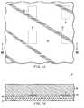
- FIG. 1Ais a top view of a portion of a substrate
- FIG. 1Bis a cross-sectional view taken generally along lines 1 B- 1 B in FIG. 1A ;
- FIG. 2Ais a top view of the substrate of FIG. 1A at a subsequent fabrication stage
- FIG. 2Bis a cross-sectional view taken generally along lines 2 B- 2 B in FIG. 2A ;
- FIG. 3Ais a top view similar to FIG. 2A at a subsequent fabrication stage
- FIG. 3Bis a cross-sectional view taken generally along lines 3 B- 3 B in FIG. 3A ;
- FIG. 4Ais a top view similar to FIG. 3A at a subsequent fabrication stage
- FIG. 4Bis a cross-sectional view taken generally along lines 4 B- 4 B in FIG. 4A ;
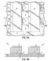
- FIG. 5Ais a top view similar to FIG. 4A at a subsequent fabrication stage
- FIG. 5Bis a cross-sectional view taken generally along lines 5 B- 5 B in FIG. 5A ;
- FIG. 6Ais a top view similar to FIG. 5A at a subsequent fabrication stage
- FIG. 6Bis a cross-sectional view taken generally along lines 6 B- 6 B in FIG. 6A ;
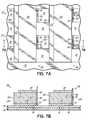
- FIG. 7Ais a top view similar to FIG. 6A at a subsequent fabrication stage
- FIG. 7Bis a cross-sectional view taken generally along lines 7 B- 7 B in FIG. 7A ;
- FIG. 8Ais a top view similar to FIG. 7A at a subsequent fabrication stage
- FIG. 8Bis a cross-sectional view taken generally along lines 8 B- 8 B in FIG. 8A ;
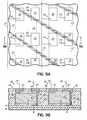
- FIG. 9Ais a top view similar to FIG. 8A at a subsequent fabrication stage
- FIG. 9Bis a cross-sectional view taken generally along lines 9 B- 9 B in FIG. 9A ;
- FIG. 10Ais a top view similar to FIG. 9A of a device structure in accordance with an alternative embodiment of the invention.
- FIG. 10Bis a cross-sectional view taken generally along lines 10 B- 10 B in FIG. 10A ;
- FIG. 11Ais a top view similar to FIG. 10A of a device structure in accordance with an alternative embodiment of the invention.
- FIG. 11Bis a cross-sectional view taken generally along lines 11 B- 11 B in FIG. 11A ;
- FIG. 12Ais a top view similar to FIG. 1A of a device structure in accordance with an alternative embodiment of the invention.
- FIG. 12Bis a cross-sectional view taken generally along lines 12 B- 12 B in FIG. 12A .
- the inventionin its various embodiments provides methods for forming arrays of field effect transistors (FET's) incorporating semiconducting carbon nanotubes as a channel region and, optionally, conducting carbon nanotubes as a component of a gate contact and/or a source contact.
- FET'sfield effect transistors
- Adjacent FET'sare spaced apart such that, as the carbon nanotubes lengthen, the flow of CVD reactant(s) to a catalyst material supporting nanotube synthesis does not become restricted. Because the nanotube synthesis is unencumbered by significant flow restrictions, the carbon nanotubes may be grown at a higher rate to a greater length, and arrays of FET's may be formed by appropriate mass production techniques.
- a layer stack 10is formed on a substrate 12 covered by multiple parallel rows or stripes of a conductive layer 14 composed of a conducting material that participates in a source/drain connection in the completed device structure 54 ( FIGS. 9A and 9B ).
- Substrate 12may be composed of any suitable substrate material, including but not limited to silicon (Si), gallium arsenide (GaAs), glasses, silicon carbide (SiC), and silicon dioxide (SiO 2 ). If substrate 12 is composed of a conducting material, then it must be covered by an insulating material (not shown) so that the discrete device structures 54 are not shorted together after fabrication.
- the layer stack 10includes a patterned layer of catalyst pads 16 separated from a gate conductor 18 by an insulating layer 20 .
- the gate conductor 18consists of a blanket layer of a conductive material, such as highly-doped polycrystalline silicon (polysilicon) deposited by a low pressure chemical vapor deposition (LPCVD) process.
- the insulating layer 20is formed from a thin film of an insulating material, such as SiO 2 , silicon nitride (Si 3 N 4 ) or silicon oxynitride (SiO x N y ), deposited by any suitable conventional deposition technique.
- the material forming substrate 12 , conductive layer 14 and gate conductor 18do not catalyze synthesis of carbon nanotubes.
- the catalyst pads 16are formed by depositing a blanket layer of the catalytic material by any conventional deposition technique including, but not limited to, a chemical vapor deposition (CVD) process using suitable precursors such as metal halides and metal carbonyls, sputtering, and physical vapor deposition (PVD), and then employing a standard lithographic and subtractive etch process to pattern the blanket layer.
- CVDchemical vapor deposition
- PVDphysical vapor deposition
- Catalyst pads 16which are electrically conducting, are positioned so that the stripes of conductive layer 14 are not shorted to one other.
- the catalytic material in catalyst pads 16is any material capable of nucleating and supporting the synthesis or growth of semiconducting carbon nanotubes when exposed to appropriate reactants under chemical reaction conditions suitable to promote nanotube growth.
- Suitable catalytic materials for catalyst pads 16include, but are not limited to, iron, nickel, cobalt, compounds of these metals such as metal oxides and metal silicides, and alloys of these metals. In the case of metal oxides, it may be necessary to perform a reduction to access or activate the catalyst material.
- the catalyst material or a material alloyed with the catalyst materialsuch as transition metals, potassium, rubidium, or arsenic pentafluoride (AsF 5 ), may also be capable of selectively diffusing from catalyst pad 16 into synthesized semiconducting carbon nanotubes 42 ( FIGS. 7A and 7B ), under appropriate conditions, for increasing the electrical conductivity of the diffused region, as explained below.
- references herein to terms such as “vertical”, “horizontal”, etc.are made by way of example, and not by way of limitation, to establish a frame of reference.
- the term “horizontal” as used hereinis defined as a plane parallel to the conventional plane or surface of substrate 12 , regardless of orientation.
- the term “vertical”refers to a direction perpendicular to the horizontal, as just defined. Terms, such as “on”, “above”, “below”, “side” (as in “sidewall”), “higher”, “lower”, “over”, “beneath” and “under”, are defined with respect to the horizontal plane. It is understood that various other frames of reference may be employed without departing from the spirit and scope of the invention.
- an insulating layer 24is deposited on the gate conductor 18 and patterned by a standard lithographic and etch process.
- the insulating layer 24is formed of a thin film of an insulating material, such as SiO 2 , Si 3 N 4 or SiO x N y , that does not catalyze synthesis of carbon nanotubes.
- Insulating layer 24may be deposited by any suitable conventional deposition technique. Insulating layers 20 and 24 should be thin for optimizing device performance.
- the layer stack 10( FIGS. 2A and 2B ) is patterned to form an array of substantially identical, parallel columnar gate electrodes 25 running orthogonally to the stripes of conductive layer 14 that cooperate to define a rectangular grid of device structures 54 ( FIGS. 9A and 9B ).
- vertically-aligned portions of the insulating layer 24 and the gate conductor 18are removed by a standard lithographic and etch process that also exposes regions of the catalyst pads 16 and conductive layer 14 .
- Insulating layer 20electrically isolates each gate electrode 25 from the conductive layer 14 .
- each of the gate electrodes 25defines a word line 26 for selecting all device structures 54 in a corresponding column of device structures 54 .
- FIGS. 3A and 3Bthe invention is not so limited, as any number of gate electrodes 25 may be defined in gate conductor 18 to comply with a specific circuit design.
- Adjacent stripes of the conductive layer 14are each separated by one of multiple parallel stripes of insulating layer 12 , which are exposed when portions of the insulating layer 20 and gate conductor 18 are removed.
- the stripes of conductive layer 14define bit lines 27 for selecting all device structures 54 in a corresponding row of device structures 54 .
- the word lines 26 and bit lines 27are interfaced with suitable circuitry (not shown) to read or address a specific device structure 54 at the intersection of a selected word line 26 and a selected bit line 27 .
- suitable circuitrynot shown
- a temporary spacer 28which may be composed of SiO 2 or SiO x N y , is formed that covers the vertical surfaces of catalyst pads 16 , insulating layer 20 , and the gate electrodes 25 .
- the thickness or width of temporary spacer 28determines, after etching, a catalyst site or active area 34 of each of the catalyst pads 16 that is eventually exposed to the reactant(s) for synthesizing carbon nanotubes.
- the size of the active area 34is believed to be a factor in determining the dimensions of the semiconducting carbon nanotubes 42 ( FIGS. 7A and 7B ) synthesized thereon.
- the width of the active areas 34is on the order of a few nanometers.
- the active areas 34are defined by removing portions of the catalyst pads 16 not masked by the temporary spacer 28 using either a wet or dry etch process as understood by persons of ordinary skill in the art. Active areas 34 are revealed by removing the temporary spacer 28 with either a wet or dry etch process as understood by persons of ordinary skill in the art. Following the etch processes, the resultant structure includes an array of active areas 34 each having a desired feature size. One column of active areas 34 is aligned with each gate electrode 25 .
- the catalyst pads 16are deposited with a monolayer thickness and annealed to create nanocrystals.
- the smaller nanocrystalsmay lead to the synthesis of smaller diameter nanotubes 42 ( FIGS. 7A and 7B ) and may favor the synthesis of single-wall carbon nanotubes 42 .
- an insulating layer 38is applied to the vertical surfaces of each gate electrode 25 .
- the insulating layer 38may be composed of any suitable insulating or dielectric material, such as SiO 2 either grown by an oxidation process or deposited by a CVD process.
- the insulating layer 38serves as a gate dielectric in the completed device structure 54 ( FIGS. 10A and 10B ).
- the word lines 26are arranged as parallel columns and the bit lines 27 are arranged in parallel rows with adjacent word lines 26 separated by one of a corresponding plurality of open volumes or spaces 39 that supply reactant flow paths to the active areas 34 .
- the ratio of the area defined by open spaces 39 to the total area viewed in a direction normal or perpendicular to substrate 12is between about 20 percent and about 50 percent, preferably about 33 percent.
- the formation of insulating layer 38may oxidize or otherwise inactivate the catalyst material forming active areas 34 .
- the oxidized catalyst materialmay be reduced using hydrogen or forming gas at a temperature of about 300° C. to about 600° C., which is selected to avoid potentially reducing insulating layer 38 .
- carbon nanotubes 42are grown or synthesized on active areas 34 by a CVD process.
- the length of the carbon nanotubes 42is typically about 50 nm to about 500 nm, which corresponds approximately to the vertical height of the gate electrode 25 .
- An optional spacer(not shown) may be applied about the vertical surfaces of the active areas 34 of catalyst pads 16 to eliminate nanotube synthesis from those vertical surfaces, which might potentially occlude the open spaces 39 and/or unwantedly create undesirable electrical connections by extending between adjacent word lines 26 or adjacent bit lines 27 .
- the conductive layer 14 exposed in open spaces 39is composed of a conducting material that supports nanotube synthesis, a layer (not shown) of a temporary masking material must be applied to cover the exposed horizontal surfaces of conducting layer 14 during nanotube synthesis and then removed following nanotube synthesis.
- Each active area 34supports the synthesis of one or more semiconducting carbon nanotubes 42 .
- the nanotube synthesis conditions and reactant(s) and/or the types of catalyst material constituting catalyst pads 16are chosen to selectively grow semiconducting carbon nanotubes 42 on active areas 34 .
- semiconducting carbon nanotubes 42 on active areas 34may be preferentially selected from among a collection of as-grown nanotubes 42 including both conducting and semiconducting molecular structures by, for example, applying a current sufficiently high to destroy nanotubes 42 having a conducting molecular structure.
- An exemplary approach for post-synthesis destruction of conducting carbon nanotubesis described in commonly-assigned U.S. Pat. No. 6,423,583, which is hereby incorporated by reference herein in its entirety.
- Carbon nanotubes 42constitute hollow cylindrical tubes of precisely arranged hexagonal rings of bonded carbon atoms having a structure characterized by a semiconducting electronic state.
- the cylindrical tubesmay have a diameter ranging from about 0.5 nm to many nanometers as limited by the dimensions of the active area 34 and, if multi-wall, may have a sidewall thickness of several nanometers.
- the carbon nanotubes 42may, without limitation, be multi-wall nanotubes resembling concentric cylinders or, alternatively, may constitute single-wall nanotubes.
- the carbon nanotubes 42extend upward from the corresponding active areas 34 with a vertical or, at the least, a substantially vertical orientation as the invention contemplates minor deviations from verticality (e.g., tilting) in growth direction may occur.
- the lengthening carbon nanotubes 42will closely spatially follow or conform to the adjacent vertical surface of the gate electrode 25 .
- the vertical directionality of nanotubes 42is expected to be particularly evident for plasma enhanced CVD in which the nanotubes 42 may lengthen in the direction of an electric field present in the open spaces 39 .
- van der Waals forceswill operate to attract the lengthening carbon nanotubes 42 to the vertical surface of the insulating layer 38 .
- the CVD process or plasma-enhanced CVD process synthesizing the carbon nanotubes 42relies on any suitable gaseous or vaporized carbonaceous reactant(s) including, but not limited to, carbon monoxide (CO), ethylene (C 2 H 4 ), methane (CH 4 ), acetylene (C 2 H 2 ), xylene (C 6 H 4 (CH 3 ) 2 ), a mixture of C 2 H 2 and ammonia (NH 3 ), a mixture of C 2 H 2 and nitrogen (N 2 ), a mixture of C 2 H 2 and hydrogen (H 2 ), and a mixture of ethanol (C 2 H 6 O) and N 2 , supplied under growth conditions suitable for promoting carbon nanotube growth on the catalytic material forming the catalyst pads 16 .
- any suitable gaseous or vaporized carbonaceous reactant(s)including, but not limited to, carbon monoxide (CO), ethylene (C 2 H 4 ), methane (CH 4 ), acetylene (C 2
- Substrate 12may be heated to a temperature adequate to promote and/or hasten CVD growth.
- the reactant(s)are delivered or supplied to each active area 34 , where the reactant chemically reacts with the catalyst material to nucleate carbon nanotubes 42 and to sustain their growth following nucleation.
- the reactant(s)freely flow without significant flow constrictions in the volume defined by the open spaces 39 between word lines 26 to the active areas 34 for participating in the synthesis of semiconducting carbon nanotubes 42 . Synthesis is expected to occur by addition of carbon atoms at an interface between each of the carbon nanotubes 42 and the corresponding active area 34 .
- the catalyst material of the catalyst pads 16participates in and promotes carbon nanotube synthesis without itself being transformed or consumed by the chemical reaction transpiring at its exposed surface by reducing the activation energy of the reaction forming semiconducting carbon nanotubes 42 .
- atoms originating from the catalyst material or from a material alloyed with the catalyst materialmay be diffused into a region of length of the semiconducting carbon nanotubes 42 .
- the presence of the diffused specieswould increase the electrical conductivity of the semiconducting carbon nanotubes 42 in the diffused region of length, which is preferably approximately equal to the thickness of insulating layer 20 .
- the diffusionwould be performed at a temperature higher than the temperature during nanotube synthesis, which controllably promotes diffusion only after the carbon nanotubes 42 are synthesized.
- the conduction-increasing speciesis not transferred from the active areas 34 of catalyst material into the carbon nanotubes 42 during synthesis, which might otherwise compromise the semiconducting properties of the nanotubes 42 for lengths of nanotubes 42 horizontally aligned with the gate electrode 25 .
- a fill layer 46 of a dielectric materialis conformally deposited by a conventional process to fill the open spaces 39 between adjacent word lines 26 and any spaces, if present, between adjacent semiconducting carbon nanotubes 42 .
- the fill layer 46may be, for example, SiO 2 deposited by a CVD process or a spin-on glass characterized by a low dielectric constant. Fill layer 46 stabilizes the position of the carbon nanotubes 42 either contacting or proximate to insulating layer 38 .
- Fill layer 46is polished flat by CMP or any other suitable planarization technique and another insulating layer 48 , such as SiO 2 , is deposited on planarized fill layer 46 .
- the polishingremoves fill layer 46 to a depth sufficient to also shorten lengthy nanotubes 42 projecting above the horizontal plane of an upper surface of insulating layer 24 .
- source/drain contacts 50 electrically coupled with the semiconducting carbon nanotubes 42 and gate contacts 52 electrically coupled with the gate electrode 25are formed by defining contact openings in insulating layer 48 by a standard lithographic and etch process, optionally lining the contact openings with one or more barrier/adhesion enhancement layers (not shown), and blanket depositing a metal, such as tungsten, to fill the contact openings with metal plugs, and then removing the excess overburden of conductive material by any suitable planarization technique, such as CMP.
- CMPplanarization technique
- the resultant structureis a memory circuit including memory device structures 54 arranged as an interconnected row and column array of field effect transistors each including a gate defined by gate electrode 25 , source/drain contact 50 , a second source/drain contact defined by catalyst pad 16 and the stripes of conductive layer 14 , a gate dielectric defined by insulating layer 38 , and a semiconducting channel region defined along the length of the semiconducting carbon nanotubes 42 .
- Each completed device structure 54is electrically coupled for operation in the memory circuit with other device structures 54 supported on adjacent regions of the substrate 12 .
- a plurality of capacitors 55 and a plurality of capacitors 56are electrically coupled with drain contacts 50 in different word lines 26 for charge storage.
- This structureis described in more detail, for example, in S. Arai et al., IEEE IEDM 01-403 (2001), which is hereby incorporated by reference herein in its entirety.
- Currentflows selectively from the catalyst pad 16 through the carbon nanotubes 42 for storing charge in the capacitor 56 when a sufficient electrical voltage is applied to an appropriate word line 26 from one of conductive lines 57 , 59 .
- the memory device structures 54are electrically coupled by the stripes of conductive layer 14 (e.g., bit lines 27 ) and the gate electrodes 25 (e.g., word lines 26 ), which are used to read and write the binary state of the memory device structures 54 .
- a memory device structure 58includes a second patterned layer of catalyst pads 22 provided at a location generally overlying the gate conductor 18 ( FIGS. 1A and 1B ) and underlying the insulating layer 24 ( FIGS. 2A and 2B ) in the layer stack 10 .
- the catalytic material constituting catalyst pads 22is any electrically conducting material capable of nucleating and supporting the synthesis or growth of carbon nanotubes 44 when exposed to appropriate reactants under chemical reaction conditions suitable to promote nanotube growth. Suitable catalytic materials for catalyst pads 22 are described above with regard to catalyst pads 16 .
- One or more carbon nanotubes 44are grown or synthesized by a CVD growth process on catalyst pads 22 .
- the synthesis conditions characterizing the CVD growth processmay be modified to preferentially grow conducting carbon nanotubes 44 .
- the length of carbon nanotubes 44is typically about 10 nm to about 100 nm.
- Gate contacts 60which replace gate contacts 52 , are electrically coupled with the carbon nanotubes 44 and, hence, are electrically coupled with a corresponding one of gate electrodes 25 .
- contact openingsare defined in insulating layer 24 , fill layer 46 , and insulating layer 48 by a standard lithographic and etch process to expose the catalyst pads 22 subsequent to a fabrication stage corresponding to FIGS. 8A and 8B .
- the carbon nanotubes 44are synthesized by the CVD growth process and the contact openings are filled with metal plugs to provide the gate contacts 60 .
- the carbon nanotubes 44project vertically into the bulk of the corresponding gate contacts 60 after the contact openings are filled with corresponding metal plugs.
- Insulating layer 24is shortened horizontally such that the vertical edge of the layer 24 is withdrawn from the vertical surface of gate electrode 25 overlying the active area 34 .
- the reduced width of the insulating layer 24also reduces the likelihood that a free end of bent carbon nanotubes 42 ( FIGS. 8A and 8B ) formed on catalyst pad 16 can contact a vertical surface of insulating layer 24 and thereby be spaced away from the vertical surface of the gate electrode 25 .
- conductive layer 14 of a logic device structure 74is etched at a fabrication stage equivalent to the fabrication stage of FIGS. 1A and 1B to define discontinuities in the layer striping, which are ultimately filled with portions of fill layer 46 .
- adjacent device structures 74are electrically isolated unless intentionally interconnected in the completed device structure to form a logic circuit.
- the device structures 74are constructed from layer stack 10 ( FIGS.
- gate electrodes 66modified by patterning the gate conductor 18 using standard lithographic and etch processes to define an array of substantially identical gate electrodes 66 configured as spaced apart islands.
- the gate electrodes 66are arranged as columns and rows of an array in which adjacent gate electrodes 66 are separated by one of a corresponding plurality of open spaces 39 that supply reactant flow paths to a corresponding one of the active areas 34 during growth of the semiconducting carbon nanotubes 42 .
- Source/drain contacts 68 electrically coupled with one end of the semiconducting carbon nanotubes 42 , metal posts 80 electrically coupled with a conducting pad 76 to define a source connection via conducting layer 14 with an opposite end of the semiconducting carbon nanotubes 42 , and gate contacts 70 electrically coupled with each gate electrode 66are formed by standard lithographic and etch processes in insulating layer 48 .
- One truncated stripe of conducting layer 14extends horizontally beneath each gate electrode 66 from the corresponding metal post 80 to electrically couple with the associated catalyst pad 16 .
- the truncated stripe of conducting layer 14 , the catalyst pad 16 and the metal post 80collectively form a second source/drain contact.
- Conductive metallization lines 82 , 84 , and 86interconnect the source/drain contacts 68 , the gate contacts 70 and the metal posts 80 , respectively, for operation as a logic circuit as understood by persons of ordinary skill in the art.
- a logic device structure 88further includes catalyst pads 76 each formed from a catalyst material capable of supporting the growth of at least one conducting carbon nanotube 90 .
- Catalyst pads 76which are electrically conducting, are introduced into layer stack 10 by the process forming catalyst pads 16 :
- Carbon nanotubes 90of which at least a fraction have a conducting electronic state, are synthesized at a fabrication stage corresponding to the fabrication stage of FIGS. 7A and 7B at which the semiconducting carbon nanotubes 42 and, optionally, carbon nanotubes 44 ( FIGS.
- Source/drain contacts 92formed by a standard lithographic and etch process in the insulating layer 48 are electrically coupled with the conducting carbon nanotubes 90 .
- the free ends of the carbon nanotubes 90extend into the bulk of the source/drain contacts 92 .
- the source/drain contacts 68 , the gate contacts 70 and the source/drain contacts 92are interconnected by conductive metallization lines 82 , 84 , and 86 , respectively, for operation as a logic circuit as understood by persons of ordinary skill in the art.
- the inventioncontemplates that the gate contacts 70 may be also formed partially by conducting carbon nanotubes (not shown but similar to carbon nanotubes 44 depicted in FIGS. 10A and 10B ).
Landscapes
- Engineering & Computer Science (AREA)
- Chemical & Material Sciences (AREA)
- Nanotechnology (AREA)
- Materials Engineering (AREA)
- Physics & Mathematics (AREA)
- Mathematical Physics (AREA)
- Theoretical Computer Science (AREA)
- Crystallography & Structural Chemistry (AREA)
- General Physics & Mathematics (AREA)
- Manufacturing & Machinery (AREA)
- Computer Hardware Design (AREA)
- Microelectronics & Electronic Packaging (AREA)
- Power Engineering (AREA)
- Condensed Matter Physics & Semiconductors (AREA)
- Thin Film Transistor (AREA)
- Semiconductor Memories (AREA)
- Carbon And Carbon Compounds (AREA)
- Electrodes Of Semiconductors (AREA)
- Metal-Oxide And Bipolar Metal-Oxide Semiconductor Integrated Circuits (AREA)
Abstract
Description
Claims (24)
Priority Applications (10)
| Application Number | Priority Date | Filing Date | Title |
|---|---|---|---|
| US10/777,576US7829883B2 (en) | 2004-02-12 | 2004-02-12 | Vertical carbon nanotube field effect transistors and arrays |
| TW094103739ATWI344662B (en) | 2004-02-12 | 2005-02-04 | Methods of fabricating vertical carbon nanotube field effect transistors for arrangement in arrays and field effect transistors and arrays formed thereby |
| DE602005027316TDE602005027316D1 (en) | 2004-02-12 | 2005-02-10 | METHOD FOR PRODUCING VERTICAL CARBON NANOROUS FIELD EFFECT TRANSISTORS FOR ARRAYS ARRANGEMENT AND FIELD EFFECT TRANSISTORS AND ARRAYS MADE THEREWITH |
| PCT/EP2005/050591WO2005078819A1 (en) | 2004-02-12 | 2005-02-10 | Methods of fabricating vertical carbon nanotube field effect transistors for arrangement in arrays and field effect transistors and arrays formed thereby |
| JP2006552625AJP5089174B2 (en) | 2004-02-12 | 2005-02-10 | Method for manufacturing a circuit including an array of semiconductor device structures |
| EP05707994AEP1714330B1 (en) | 2004-02-12 | 2005-02-10 | Methods of fabricating vertical carbon nanotube field effect transistors for arrangement in arrays and field effect transistors and arrays formed thereby |
| AT05707994TATE504946T1 (en) | 2004-02-12 | 2005-02-10 | METHOD FOR PRODUCING VERTICAL CARBON NANOTUBE FIELD EFFECT TRANSISTORS FOR ARRANGEMENT IN ARRAYS AND FIELD EFFECT TRANSISTORS AND ARRAYS FORMED THEREFROM |
| KR1020067015500AKR100992296B1 (en) | 2004-02-12 | 2005-02-10 | Method for manufacturing vertical carbon nanotube field effect transistor in array array and field effect transistor and array formed thereby |
| CN2005800046714ACN1943055B (en) | 2004-02-12 | 2005-02-10 | Semiconductor device structure and methods of fabricating array including the structure |
| US11/926,627US7820502B2 (en) | 2004-02-12 | 2007-10-29 | Methods of fabricating vertical carbon nanotube field effect transistors for arrangement in arrays and field effect transistors and arrays formed thereby |
Applications Claiming Priority (1)
| Application Number | Priority Date | Filing Date | Title |
|---|---|---|---|
| US10/777,576US7829883B2 (en) | 2004-02-12 | 2004-02-12 | Vertical carbon nanotube field effect transistors and arrays |
Related Child Applications (1)
| Application Number | Title | Priority Date | Filing Date |
|---|---|---|---|
| US11/926,627DivisionUS7820502B2 (en) | 2004-02-12 | 2007-10-29 | Methods of fabricating vertical carbon nanotube field effect transistors for arrangement in arrays and field effect transistors and arrays formed thereby |
Publications (2)
| Publication Number | Publication Date |
|---|---|
| US20050179029A1 US20050179029A1 (en) | 2005-08-18 |
| US7829883B2true US7829883B2 (en) | 2010-11-09 |
Family
ID=34838018
Family Applications (2)
| Application Number | Title | Priority Date | Filing Date |
|---|---|---|---|
| US10/777,576Expired - Fee RelatedUS7829883B2 (en) | 2004-02-12 | 2004-02-12 | Vertical carbon nanotube field effect transistors and arrays |
| US11/926,627Expired - Fee RelatedUS7820502B2 (en) | 2004-02-12 | 2007-10-29 | Methods of fabricating vertical carbon nanotube field effect transistors for arrangement in arrays and field effect transistors and arrays formed thereby |
Family Applications After (1)
| Application Number | Title | Priority Date | Filing Date |
|---|---|---|---|
| US11/926,627Expired - Fee RelatedUS7820502B2 (en) | 2004-02-12 | 2007-10-29 | Methods of fabricating vertical carbon nanotube field effect transistors for arrangement in arrays and field effect transistors and arrays formed thereby |
Country Status (9)
| Country | Link |
|---|---|
| US (2) | US7829883B2 (en) |
| EP (1) | EP1714330B1 (en) |
| JP (1) | JP5089174B2 (en) |
| KR (1) | KR100992296B1 (en) |
| CN (1) | CN1943055B (en) |
| AT (1) | ATE504946T1 (en) |
| DE (1) | DE602005027316D1 (en) |
| TW (1) | TWI344662B (en) |
| WO (1) | WO2005078819A1 (en) |
Cited By (3)
| Publication number | Priority date | Publication date | Assignee | Title |
|---|---|---|---|---|
| US20090213830A1 (en)* | 2004-10-11 | 2009-08-27 | Qimonda Ag | Communication system |
| WO2012158996A1 (en)* | 2011-05-19 | 2012-11-22 | International Business Machines Corporation | Self-aligned carbon electronics with embedded gate electrode |
| US8772782B2 (en) | 2011-11-23 | 2014-07-08 | International Business Machines Corporation | Transistor employing vertically stacked self-aligned carbon nanotubes |
Families Citing this family (29)
| Publication number | Priority date | Publication date | Assignee | Title |
|---|---|---|---|---|
| US7374793B2 (en)* | 2003-12-11 | 2008-05-20 | International Business Machines Corporation | Methods and structures for promoting stable synthesis of carbon nanotubes |
| US7038299B2 (en) | 2003-12-11 | 2006-05-02 | International Business Machines Corporation | Selective synthesis of semiconducting carbon nanotubes |
| US20050167655A1 (en)* | 2004-01-29 | 2005-08-04 | International Business Machines Corporation | Vertical nanotube semiconductor device structures and methods of forming the same |
| US7211844B2 (en) | 2004-01-29 | 2007-05-01 | International Business Machines Corporation | Vertical field effect transistors incorporating semiconducting nanotubes grown in a spacer-defined passage |
| US7109546B2 (en) | 2004-06-29 | 2006-09-19 | International Business Machines Corporation | Horizontal memory gain cells |
| US7233071B2 (en) | 2004-10-04 | 2007-06-19 | International Business Machines Corporation | Low-k dielectric layer based upon carbon nanostructures |
| TWI324773B (en) | 2005-05-09 | 2010-05-11 | Nantero Inc | Non-volatile shadow latch using a nanotube switch |
| US7394687B2 (en) | 2005-05-09 | 2008-07-01 | Nantero, Inc. | Non-volatile-shadow latch using a nanotube switch |
| US7781862B2 (en)* | 2005-05-09 | 2010-08-24 | Nantero, Inc. | Two-terminal nanotube devices and systems and methods of making same |
| US7479654B2 (en) | 2005-05-09 | 2009-01-20 | Nantero, Inc. | Memory arrays using nanotube articles with reprogrammable resistance |
| WO2007092770A2 (en)* | 2006-02-02 | 2007-08-16 | William Marsh Rice University | Fabrication de dispositifs electriques par façonnage de nanotubes |
| WO2007092835A2 (en)* | 2006-02-07 | 2007-08-16 | William Marsh Rice University | Production de reseaux verticaux de nanotubes de carbone a petit diametre et paroi simple |
| US20070183189A1 (en)* | 2006-02-08 | 2007-08-09 | Thomas Nirschl | Memory having nanotube transistor access device |
| US7626190B2 (en)* | 2006-06-02 | 2009-12-01 | Infineon Technologies Ag | Memory device, in particular phase change random access memory device with transistor, and method for fabricating a memory device |
| JP2009540333A (en)* | 2006-06-12 | 2009-11-19 | プレジデント アンド フェロウズ オブ ハーバード カレッジ | Nanosensors and related technologies |
| KR100803690B1 (en)* | 2006-08-10 | 2008-02-20 | 삼성전자주식회사 | Electro-mechanical nonvolatile memory device and method of manufacturing the same. |
| KR100781972B1 (en)* | 2006-09-18 | 2007-12-06 | 삼성전자주식회사 | Memory device and manufacturing method thereof |
| US20080272361A1 (en)* | 2007-05-02 | 2008-11-06 | Atomate Corporation | High Density Nanotube Devices |
| KR101478540B1 (en)* | 2007-09-17 | 2015-01-02 | 삼성전자 주식회사 | A biosensor using nanomaterials as a channel of a transistor and a manufacturing method thereof |
| US7892956B2 (en)* | 2007-09-24 | 2011-02-22 | International Business Machines Corporation | Methods of manufacture of vertical nanowire FET devices |
| US8395901B2 (en)* | 2007-11-13 | 2013-03-12 | William Marsh Rice University | Vertically-stacked electronic devices having conductive carbon films |
| JP5256850B2 (en)* | 2008-05-29 | 2013-08-07 | ミツミ電機株式会社 | Field effect transistor and manufacturing method thereof |
| US8350360B1 (en) | 2009-08-28 | 2013-01-08 | Lockheed Martin Corporation | Four-terminal carbon nanotube capacitors |
| US8405189B1 (en)* | 2010-02-08 | 2013-03-26 | Lockheed Martin Corporation | Carbon nanotube (CNT) capacitors and devices integrated with CNT capacitors |
| EP2363958A1 (en)* | 2010-03-04 | 2011-09-07 | Thomson Licensing | Field programmable gate array |
| CN104576321A (en)* | 2015-01-30 | 2015-04-29 | 京东方科技集团股份有限公司 | Electrode structure, manufacturing method thereof, display substrate and display device |
| CN107572504B (en)* | 2016-07-05 | 2020-07-10 | 中国科学院金属研究所 | A kind of preparation method of flexible thin-layer carbon-covered carbon nanotube vertical array |
| CN206067049U (en) | 2016-07-29 | 2017-04-05 | 合肥鑫晟光电科技有限公司 | Membrane material and coat peeling unit |
| US11417729B2 (en)* | 2019-08-29 | 2022-08-16 | Taiwan Semiconductor Manufacturing Company, Ltd. | Transistors with channels formed of low-dimensional materials and method forming same |
Citations (24)
| Publication number | Priority date | Publication date | Assignee | Title |
|---|---|---|---|---|
| US5796573A (en) | 1997-05-29 | 1998-08-18 | International Business Machines Corporation | Overhanging separator for self-defining stacked capacitor |
| US6250984B1 (en) | 1999-01-25 | 2001-06-26 | Agere Systems Guardian Corp. | Article comprising enhanced nanotube emitter structure and process for fabricating article |
| US20020001905A1 (en) | 2000-06-27 | 2002-01-03 | Choi Won-Bong | Vertical nano-size transistor using carbon nanotubes and manufacturing method thereof |
| US6423583B1 (en) | 2001-01-03 | 2002-07-23 | International Business Machines Corporation | Methodology for electrically induced selective breakdown of nanotubes |
| US20020163079A1 (en) | 2001-05-02 | 2002-11-07 | Fujitsu Limited | Integrated circuit device and method of producing the same |
| US6515325B1 (en) | 2002-03-06 | 2003-02-04 | Micron Technology, Inc. | Nanotube semiconductor devices and methods for making the same |
| US20030132461A1 (en) | 2000-07-28 | 2003-07-17 | Wolfgang Roesner | Field-effect transistor, circuit configuration and method of fabricating a field-effect transistor |
| EP1331671A1 (en) | 2000-11-01 | 2003-07-30 | Japan Science and Technology Corporation | Point contact array, not circuit, and electronic circuit comprising the same |
| WO2003063208A2 (en) | 2002-01-18 | 2003-07-31 | California Institute Of Technology | Array-based architecture for molecular electronics |
| US20030170930A1 (en) | 2002-02-09 | 2003-09-11 | Samsung Electronics Co., Ltd. | Memory device utilizing carbon nanotubes and method of fabricating the memory device |
| US20030178617A1 (en) | 2002-03-20 | 2003-09-25 | International Business Machines Corporation | Self-aligned nanotube field effect transistor and method of fabricating same |
| EP1361608A2 (en) | 2002-05-10 | 2003-11-12 | Texas Instruments Incorporated | Providing electrical connection between an active region and a conductive layer in a semiconductor device using carbon nanotubes |
| US20040027889A1 (en)* | 2002-02-25 | 2004-02-12 | Stmicroelectronics S.R.L. | Optically readable molecular memory obtained using carbon nanotubes, and method for storing information in said molecular memory |
| WO2004040668A2 (en) | 2002-10-31 | 2004-05-13 | Infineon Technologies Ag | Field effect transistor assembly and an integrated circuit array |
| WO2004040616A2 (en) | 2002-10-29 | 2004-05-13 | Hahn-Meitner-Institut Berlin Gmbh | Field effect transistor and method for production thereof |
| EP1420414A1 (en) | 2002-11-15 | 2004-05-19 | Samsung Electronics Co., Ltd. | Nonvolatile memory device utilising vertical nanotube |
| EP1435660A2 (en) | 2002-12-30 | 2004-07-07 | Samsung Electronics Co., Ltd. | Memory device utilizing vertical nanotubes |
| WO2004105140A1 (en) | 2003-05-22 | 2004-12-02 | Fujitsu Limited | Field-effect transistor and its manufacturing method |
| US20050129948A1 (en) | 2003-12-11 | 2005-06-16 | International Business Machines Corporation | Methods and structures for promoting stable synthesis of carbon nanotubes |
| US20050130341A1 (en) | 2003-12-11 | 2005-06-16 | International Business Machines Corporation | Selective synthesis of semiconducting carbon nanotubes |
| US20050167655A1 (en) | 2004-01-29 | 2005-08-04 | International Business Machines Corporation | Vertical nanotube semiconductor device structures and methods of forming the same |
| US20050167755A1 (en) | 2003-01-02 | 2005-08-04 | Intel Corporation | Microcircuit fabrication and interconnection |
| US20050167740A1 (en) | 2004-01-29 | 2005-08-04 | International Business Machines Corporation | Vertical field effect transistors incorporating semiconducting nanotubes grown in a spacer-defined passage |
| US6979947B2 (en) | 2002-07-09 | 2005-12-27 | Si Diamond Technology, Inc. | Nanotriode utilizing carbon nanotubes and fibers |
Family Cites Families (13)
| Publication number | Priority date | Publication date | Assignee | Title |
|---|---|---|---|---|
| US5514879A (en)* | 1990-11-20 | 1996-05-07 | Semiconductor Energy Laboratory Co., Ltd. | Gate insulated field effect transistors and method of manufacturing the same |
| JP3745392B2 (en)* | 1994-05-26 | 2006-02-15 | 株式会社ルネサステクノロジ | Semiconductor device |
| JP3730476B2 (en)* | 2000-03-31 | 2006-01-05 | 株式会社東芝 | Field emission cold cathode and manufacturing method thereof |
| SE520109C2 (en)* | 2000-05-17 | 2003-05-27 | Ericsson Telefon Ab L M | Power transistors for radio frequencies |
| US6440763B1 (en)* | 2001-03-22 | 2002-08-27 | The United States Of America As Represented By The Secretary Of The Navy | Methods for manufacture of self-aligned integrally gated nanofilament field emitter cell and array |
| JP4225716B2 (en)* | 2001-09-11 | 2009-02-18 | 富士通株式会社 | Semiconductor device with cylindrical multilayer structure |
| US6525453B2 (en)* | 2001-05-02 | 2003-02-25 | Huang Chung Cheng | Field emitting display |
| JP4416376B2 (en)* | 2002-05-13 | 2010-02-17 | 富士通株式会社 | Semiconductor device and manufacturing method thereof |
| US6830981B2 (en)* | 2002-07-02 | 2004-12-14 | Industrial Technology Research Institute | Vertical nanotube transistor and process for fabricating the same |
| CN1472814A (en)* | 2002-08-01 | 2004-02-04 | �й���ѧԺ�����о��� | Single-electron memory based on carbon nanotube single-electron transistor design and its fabrication method |
| DE10250829B4 (en)* | 2002-10-31 | 2006-11-02 | Infineon Technologies Ag | Nonvolatile memory cell, memory cell array, and method of making a nonvolatile memory cell |
| JP4071601B2 (en)* | 2002-11-11 | 2008-04-02 | 富士通株式会社 | Semiconductor device |
| JP4762522B2 (en)* | 2003-10-28 | 2011-08-31 | 株式会社半導体エネルギー研究所 | Method for manufacturing semiconductor device |
- 2004
- 2004-02-12USUS10/777,576patent/US7829883B2/ennot_activeExpired - Fee Related
- 2005
- 2005-02-04TWTW094103739Apatent/TWI344662B/ennot_activeIP Right Cessation
- 2005-02-10WOPCT/EP2005/050591patent/WO2005078819A1/enactiveApplication Filing
- 2005-02-10ATAT05707994Tpatent/ATE504946T1/ennot_activeIP Right Cessation
- 2005-02-10EPEP05707994Apatent/EP1714330B1/ennot_activeExpired - Lifetime
- 2005-02-10KRKR1020067015500Apatent/KR100992296B1/ennot_activeExpired - Fee Related
- 2005-02-10CNCN2005800046714Apatent/CN1943055B/ennot_activeExpired - Lifetime
- 2005-02-10JPJP2006552625Apatent/JP5089174B2/ennot_activeExpired - Fee Related
- 2005-02-10DEDE602005027316Tpatent/DE602005027316D1/ennot_activeExpired - Lifetime
- 2007
- 2007-10-29USUS11/926,627patent/US7820502B2/ennot_activeExpired - Fee Related
Patent Citations (32)
| Publication number | Priority date | Publication date | Assignee | Title |
|---|---|---|---|---|
| US5796573A (en) | 1997-05-29 | 1998-08-18 | International Business Machines Corporation | Overhanging separator for self-defining stacked capacitor |
| US6250984B1 (en) | 1999-01-25 | 2001-06-26 | Agere Systems Guardian Corp. | Article comprising enhanced nanotube emitter structure and process for fabricating article |
| US20030227015A1 (en) | 2000-06-27 | 2003-12-11 | Samsung Electronics Co., Ltd | Vertical nano-size transistor using carbon nanotubes and manufacturing method thereof |
| US20020001905A1 (en) | 2000-06-27 | 2002-01-03 | Choi Won-Bong | Vertical nano-size transistor using carbon nanotubes and manufacturing method thereof |
| US6566704B2 (en)* | 2000-06-27 | 2003-05-20 | Samsung Electronics Co., Ltd. | Vertical nano-size transistor using carbon nanotubes and manufacturing method thereof |
| US20030230760A1 (en) | 2000-06-27 | 2003-12-18 | Samsung Electronics Co., Ltd. | Vertical nano-size transistor using carbon nanotubes and manufacturing method thereof |
| US20030132461A1 (en) | 2000-07-28 | 2003-07-17 | Wolfgang Roesner | Field-effect transistor, circuit configuration and method of fabricating a field-effect transistor |
| EP1331671A1 (en) | 2000-11-01 | 2003-07-30 | Japan Science and Technology Corporation | Point contact array, not circuit, and electronic circuit comprising the same |
| US6423583B1 (en) | 2001-01-03 | 2002-07-23 | International Business Machines Corporation | Methodology for electrically induced selective breakdown of nanotubes |
| US20020163079A1 (en) | 2001-05-02 | 2002-11-07 | Fujitsu Limited | Integrated circuit device and method of producing the same |
| WO2003063208A2 (en) | 2002-01-18 | 2003-07-31 | California Institute Of Technology | Array-based architecture for molecular electronics |
| US20030170930A1 (en) | 2002-02-09 | 2003-09-11 | Samsung Electronics Co., Ltd. | Memory device utilizing carbon nanotubes and method of fabricating the memory device |
| US20040027889A1 (en)* | 2002-02-25 | 2004-02-12 | Stmicroelectronics S.R.L. | Optically readable molecular memory obtained using carbon nanotubes, and method for storing information in said molecular memory |
| US6858891B2 (en) | 2002-03-06 | 2005-02-22 | Micron Technology, Inc. | Nanotube semiconductor devices and methods for making the same |
| US20030168683A1 (en) | 2002-03-06 | 2003-09-11 | Micron Technology, Inc. | Nanotube semiconductor devices and methods for making the same |
| US6515325B1 (en) | 2002-03-06 | 2003-02-04 | Micron Technology, Inc. | Nanotube semiconductor devices and methods for making the same |
| US20030178617A1 (en) | 2002-03-20 | 2003-09-25 | International Business Machines Corporation | Self-aligned nanotube field effect transistor and method of fabricating same |
| US6891227B2 (en) | 2002-03-20 | 2005-05-10 | International Business Machines Corporation | Self-aligned nanotube field effect transistor and method of fabricating same |
| US20050056826A1 (en) | 2002-03-20 | 2005-03-17 | Joerg Appenzeller | Self-aligned nanotube field effect transistor and method of fabricating same |
| EP1361608A2 (en) | 2002-05-10 | 2003-11-12 | Texas Instruments Incorporated | Providing electrical connection between an active region and a conductive layer in a semiconductor device using carbon nanotubes |
| US6979947B2 (en) | 2002-07-09 | 2005-12-27 | Si Diamond Technology, Inc. | Nanotriode utilizing carbon nanotubes and fibers |
| WO2004040616A2 (en) | 2002-10-29 | 2004-05-13 | Hahn-Meitner-Institut Berlin Gmbh | Field effect transistor and method for production thereof |
| WO2004040668A2 (en) | 2002-10-31 | 2004-05-13 | Infineon Technologies Ag | Field effect transistor assembly and an integrated circuit array |
| EP1420414A1 (en) | 2002-11-15 | 2004-05-19 | Samsung Electronics Co., Ltd. | Nonvolatile memory device utilising vertical nanotube |
| EP1435660A2 (en) | 2002-12-30 | 2004-07-07 | Samsung Electronics Co., Ltd. | Memory device utilizing vertical nanotubes |
| US20050167755A1 (en) | 2003-01-02 | 2005-08-04 | Intel Corporation | Microcircuit fabrication and interconnection |
| US6933222B2 (en)* | 2003-01-02 | 2005-08-23 | Intel Corporation | Microcircuit fabrication and interconnection |
| WO2004105140A1 (en) | 2003-05-22 | 2004-12-02 | Fujitsu Limited | Field-effect transistor and its manufacturing method |
| US20050130341A1 (en) | 2003-12-11 | 2005-06-16 | International Business Machines Corporation | Selective synthesis of semiconducting carbon nanotubes |
| US20050129948A1 (en) | 2003-12-11 | 2005-06-16 | International Business Machines Corporation | Methods and structures for promoting stable synthesis of carbon nanotubes |
| US20050167655A1 (en) | 2004-01-29 | 2005-08-04 | International Business Machines Corporation | Vertical nanotube semiconductor device structures and methods of forming the same |
| US20050167740A1 (en) | 2004-01-29 | 2005-08-04 | International Business Machines Corporation | Vertical field effect transistors incorporating semiconducting nanotubes grown in a spacer-defined passage |
Non-Patent Citations (36)
| Title |
|---|
| "Carbon Nanotube Arrays: Synthesis of Dense Arrays of Well-Aligned Carbon Nanotubes Completely Filled with Titanium Carbide on Titanium Substrates," Battelle No. 12132. |
| "IBM Scientists Develop Carbon Nanotube Transistor Technology," IBM.com News, news report concerning work published in Science, vol. 292, Issue 5517, Apr. 27, 2001 entitled "Engineering Carbon Nanotubes and Nanotube Circuits Using Electrical Breakdown" by Phaeton Avouris et al. |
| "Synthesis of CNT's," http://nepp.nasa.gov/index-nasa.cfm/769/#synthesis. |
| "Tiny Nanotubes Set New Record," Nanotechweb.org, Aug. 7, 2003. |
| A. Cao et al. "Grapevine-like Growth of Single Walled Carbon Nanotubes Among Vertically Aligned Multiwalled Nanotube Arrays," Applied Physics Letters, vol. 79, No. 9, Aug. 27, 2001, pp. 1252-1254. |
| A. Chang, "Integration of Nanotubes into Devices," National Nanofabrication Users Network, Stanford Nanofabrication Facility, p. 58. |
| B. Zheng et al., "Efficient CVD Growth of Single-Walled Carbon Nanotubes on Surfaces Using Carbon Monoxide Precursor," Nano Letters, xxxx, vol. 0., No. 0, A-D, xxxx American Chemical Society, received Jun. 4, 2002, revised Jun. 26, 2002. |
| C-H Kiang, "Growth of Large-Diameter Single-Walled Carbon Nanotubes," J. Phys. Chem. A 2000, 104, 2454-2456. |
| E. Ploenjes et al., "Single-Walled Nanotube Synthesis in CO Laser Pumped Carbon Monoxice Plasmas," Ohio State University, Oct. 10, 2001. |
| E. Ploenjes et al., "Single-Walled Nanotube Synthesis in CO Laser Pumped Carbon Monoxice Plasmas," Ohio State University, Oct. 10, 2001. |
| E. Ploenjes et al., "Synthesis of Single-Walled Carbon Nanotubes in Vibrationally Non-Equilibrium Carbon Monoxide," Chemical Physics Letters 352 (2002), Feb. 6, 2002, pp. 342-357. |
| G. S. Duesberg, et al., "Way towards the scaleable integration of carbon nanotubes into silicon based technology," Diamond and Related Materials; Elsevier Science Publishers; Amsterdam, NL; vol. 13, No. 2; Feb. 1, 2004; pp. 354-361; XP004492567. |
| Georg S. Duesberg et al., Large-Scale Integration of Carbon Nanotubes into Silicon Based Microelectronics, Proceedings of SPIE vol. 5118 (2003), pp. 125-137. |
| H. Cui et al., "Growth Behavior of Carbon Nanotubes on Multilayered Metal Catalyst Film in Chemical Vapor Deposition," Chemical Physics Letters 374 (2003), pp. 222-228. |
| H. W. Zhu et al., "Direct Synthesis of Long Single-Walled Carbon Nanotube Strands," Science, vol. 296, May 3, 2002. |
| J. Gorman, "Nanoscale Networks: Superlong Nanotubes Can Form a Grid," Science News Online, May 3, 2003, vol. 163, No. 18. |
| J. Li et al., "Bottom-Up Approach for Carbon Nanotube Interconnects," NASA Ames Research Center, received Dec. 5, 2002, accepted Jan. 31, 2003. |
| J. Li et al., "Highly-Ordered Carbon Nanotube Arrays for Electronics Applications," Applied Physics Letters, vol. 75, No. 3, Jul. 19, 1999, pp. 367-369. |
| K. Teo et al., "Catalytic Synthesis of Carbon Nanotubes and Nanofibers," Encyclopedia of Nanoscience and Nanotechnology, vol. X, pp. 1-22, 2003. |
| M. Jung et al., "Growth of Carbon Nanotubes by Chemical Vapor Deposition," Elsevier Science B.V., 2001. |
| Office Action issued in related U.S. Appl. No. 11/926,627; dated as mailed on Jun. 27, 2008; 23 pages. |
| P. Collins et al., "Engineering Carbon Nanotubes and Nanotube Circuits Using Electrical Breakdown," Science, vol. 292, Apr. 27, 2001, pp. 706-709. |
| P. Collins et al., "Nanotubes for Electronics," Scientific American, Dec. 2000, pp. 62-69. |
| P. Harris, "Carbon Nanotubes and Related Structures," Cambridge University Press, 1999. |
| S. J. Wind et al., "Vertical Scaling of Carbon Nanotube Field-Effect Transistors Using Top Gate Electrodes," Applied Physics Letters, vol. 80, No. 20, May 20, 2002, pp. 3817-3819. |
| Thomas Rueckes, et al., Carbon Nanotube-Based Nonvolatile Random Access Memory for Molecular Computing, Science magazine, Jul. 7, 2000, pp. 94-97, vol. 289. |
| V. Derycke et al., "Carbon Nanotube Inter- and Intramolecular Logic Gates," Nano Letters, xxxx, vol. 0, No. 0, A-D, received Aug. 16, 2001. |
| V.N. Popov, Carbon Nanotubes: Properties and Application, Materials Science and Engineering, R. vol. R43, No. 3, pp. 61-102 (Jan. 15, 2004) (Summary only). |
| Won Bong Choi et al., "Ultrahigh-Density Nanotransistors by Using Selectively Grown Vertical Carbon Nanotubes," Applied Physics Letters, vol. 79, No. 22, Nov. 26, 2001, pp. 3696-3698. |
| Y. Mo et al., "The Growth Mechanism of Carbon Nanotubes from Thermal Cracking of Acetylene Over Nickel Catalyst Supported on Alumina," Elsevier Science B.V., 2001. |
| Y. Zhang et al., "Electric-Field-Directed Growth of Aligned Single-Walled Carbon Nanotubes," Applied Physics Letters, vol. 79, No. 19, Nov. 5, 2001. |
| Y. Zhao et al., "Film Growth of Pillars of Multi-Walled Carbon Nanotubes," J. Phys.: Condens., Matter 15 (2003), L565-L569. |
| Z. F. Ren et al., "Growth, Characterization, and Potential Applications of Periodic Carbon Nanotube Arrays," Department of Physics, Boston College, updated 2001. |
| Z. Huang et al., "Growth of Highly Oriented Carbon Nanotubes by Plasma-Enhanced Hot Filament Chemical Vapor Deposition," Applied Physics Letters, vol. 73, No. 26, Dec. 28, 1998, pp. 3845-3847. |
| Z. Ren et al., "Large Arrays of Well-Aligned Carbon Nanotubes," Proceedings of 13th International Winter School on Electronic Properties of Novel Materials, pp. 263-267, Feb. 27-Mar. 6, 1999, Kirchberg/Tirol, Austria. |
| Z. Ren et al., "Synthesis of Large Arrays of Well-Aligned Carbon Nanotubes on Glass," Science, vol. 282, Nov. 6, 1998, pp. 1105-1107. |
Cited By (10)
| Publication number | Priority date | Publication date | Assignee | Title |
|---|---|---|---|---|
| US20090213830A1 (en)* | 2004-10-11 | 2009-08-27 | Qimonda Ag | Communication system |
| US8664657B2 (en)* | 2004-10-11 | 2014-03-04 | Qimonda Ag | Electrical circuit with a nanostructure and method for producing a contact connection of a nanostructure |
| WO2012158996A1 (en)* | 2011-05-19 | 2012-11-22 | International Business Machines Corporation | Self-aligned carbon electronics with embedded gate electrode |
| US8455365B2 (en) | 2011-05-19 | 2013-06-04 | Dechao Guo | Self-aligned carbon electronics with embedded gate electrode |
| GB2504434A (en)* | 2011-05-19 | 2014-01-29 | Ibm | Self-aligned carbon electronics with embedded gate electrode |
| US8680646B2 (en) | 2011-05-19 | 2014-03-25 | International Business Machines Corporation | Self-aligned carbon electronics with embedded gate electrode |
| US8912098B2 (en) | 2011-05-19 | 2014-12-16 | International Business Machines Corporation | Self-aligned carbon electronics with embedded gate electrode |
| GB2504434B (en)* | 2011-05-19 | 2015-07-22 | Ibm | Self-aligned carbon electronics with embedded gate electrode |
| US8772782B2 (en) | 2011-11-23 | 2014-07-08 | International Business Machines Corporation | Transistor employing vertically stacked self-aligned carbon nanotubes |
| US8895371B2 (en) | 2011-11-23 | 2014-11-25 | International Business Machines Corporation | Transistor employing vertically stacked self-aligned carbon nanotubes |
Also Published As
| Publication number | Publication date |
|---|---|
| TWI344662B (en) | 2011-07-01 |
| KR20060130154A (en) | 2006-12-18 |
| EP1714330B1 (en) | 2011-04-06 |
| WO2005078819A1 (en) | 2005-08-25 |
| CN1943055B (en) | 2011-02-23 |
| US20080044954A1 (en) | 2008-02-21 |
| JP5089174B2 (en) | 2012-12-05 |
| DE602005027316D1 (en) | 2011-05-19 |
| US20050179029A1 (en) | 2005-08-18 |
| EP1714330A1 (en) | 2006-10-25 |
| US7820502B2 (en) | 2010-10-26 |
| TW200535896A (en) | 2005-11-01 |
| JP2007523477A (en) | 2007-08-16 |
| ATE504946T1 (en) | 2011-04-15 |
| KR100992296B1 (en) | 2010-11-08 |
| CN1943055A (en) | 2007-04-04 |
Similar Documents
| Publication | Publication Date | Title |
|---|---|---|
| US7820502B2 (en) | Methods of fabricating vertical carbon nanotube field effect transistors for arrangement in arrays and field effect transistors and arrays formed thereby | |
| JP5511746B2 (en) | Method for forming vertical nanotube semiconductor device structure | |
| JP4032083B2 (en) | Methods and structures to promote stable synthesis of carbon nanotubes | |
| US7211844B2 (en) | Vertical field effect transistors incorporating semiconducting nanotubes grown in a spacer-defined passage | |
| US11322440B2 (en) | Three-dimensional memory device with dielectric wall support structures and method of forming the same | |
| US20220102375A1 (en) | Three-dimensional memory device with dielectric or semiconductor wall support structures and method of forming the same | |
| CN1716608A (en) | Storage gain unit and method of manufacturing such storage gain unit | |
| MXPA06008502A (en) | Vertical field effect transistors incorporating semiconducting nanotubes grown in a spacer-defined passage |
Legal Events
| Date | Code | Title | Description |
|---|---|---|---|
| AS | Assignment | Owner name:INTERNATIONAL BUSINESS MACHINES CORPORATION, NEW Y Free format text:ASSIGNMENT OF ASSIGNORS INTEREST;ASSIGNORS:FURUKAWA, TOSHIHARU;HAKEY, MARK CHARLES;HOLMES, STEVEN JOHN;AND OTHERS;REEL/FRAME:014995/0922;SIGNING DATES FROM 20040202 TO 20040206 | |
| STCF | Information on status: patent grant | Free format text:PATENTED CASE | |
| REMI | Maintenance fee reminder mailed | ||
| FPAY | Fee payment | Year of fee payment:4 | |
| SULP | Surcharge for late payment | ||
| AS | Assignment | Owner name:GLOBALFOUNDRIES U.S. 2 LLC, NEW YORK Free format text:ASSIGNMENT OF ASSIGNORS INTEREST;ASSIGNOR:INTERNATIONAL BUSINESS MACHINES CORPORATION;REEL/FRAME:036550/0001 Effective date:20150629 | |
| AS | Assignment | Owner name:GLOBALFOUNDRIES INC., CAYMAN ISLANDS Free format text:ASSIGNMENT OF ASSIGNORS INTEREST;ASSIGNORS:GLOBALFOUNDRIES U.S. 2 LLC;GLOBALFOUNDRIES U.S. INC.;REEL/FRAME:036779/0001 Effective date:20150910 | |
| MAFP | Maintenance fee payment | Free format text:PAYMENT OF MAINTENANCE FEE, 8TH YEAR, LARGE ENTITY (ORIGINAL EVENT CODE: M1552) Year of fee payment:8 | |
| AS | Assignment | Owner name:WILMINGTON TRUST, NATIONAL ASSOCIATION, DELAWARE Free format text:SECURITY AGREEMENT;ASSIGNOR:GLOBALFOUNDRIES INC.;REEL/FRAME:049490/0001 Effective date:20181127 | |
| AS | Assignment | Owner name:GLOBALFOUNDRIES U.S. INC., CALIFORNIA Free format text:ASSIGNMENT OF ASSIGNORS INTEREST;ASSIGNOR:GLOBALFOUNDRIES INC.;REEL/FRAME:054633/0001 Effective date:20201022 | |
| AS | Assignment | Owner name:GLOBALFOUNDRIES INC., CAYMAN ISLANDS Free format text:RELEASE BY SECURED PARTY;ASSIGNOR:WILMINGTON TRUST, NATIONAL ASSOCIATION;REEL/FRAME:054636/0001 Effective date:20201117 | |
| AS | Assignment | Owner name:GLOBALFOUNDRIES U.S. INC., NEW YORK Free format text:RELEASE BY SECURED PARTY;ASSIGNOR:WILMINGTON TRUST, NATIONAL ASSOCIATION;REEL/FRAME:056987/0001 Effective date:20201117 | |
| FEPP | Fee payment procedure | Free format text:MAINTENANCE FEE REMINDER MAILED (ORIGINAL EVENT CODE: REM.); ENTITY STATUS OF PATENT OWNER: LARGE ENTITY | |
| LAPS | Lapse for failure to pay maintenance fees | Free format text:PATENT EXPIRED FOR FAILURE TO PAY MAINTENANCE FEES (ORIGINAL EVENT CODE: EXP.); ENTITY STATUS OF PATENT OWNER: LARGE ENTITY | |
| STCH | Information on status: patent discontinuation | Free format text:PATENT EXPIRED DUE TO NONPAYMENT OF MAINTENANCE FEES UNDER 37 CFR 1.362 | |
| FP | Lapsed due to failure to pay maintenance fee | Effective date:20221109 |