US7829438B2 - Edge connect wafer level stacking - Google Patents
Edge connect wafer level stackingDownload PDFInfo
- Publication number
- US7829438B2 US7829438B2US11/787,209US78720907AUS7829438B2US 7829438 B2US7829438 B2US 7829438B2US 78720907 AUS78720907 AUS 78720907AUS 7829438 B2US7829438 B2US 7829438B2
- Authority
- US
- United States
- Prior art keywords
- microelectronic
- subassembly
- wafer
- stacked
- traces
- Prior art date
- Legal status (The legal status is an assumption and is not a legal conclusion. Google has not performed a legal analysis and makes no representation as to the accuracy of the status listed.)
- Active, expires
Links
Images


Classifications
- H—ELECTRICITY
- H01—ELECTRIC ELEMENTS
- H01L—SEMICONDUCTOR DEVICES NOT COVERED BY CLASS H10
- H01L25/00—Assemblies consisting of a plurality of semiconductor or other solid state devices
- H01L25/03—Assemblies consisting of a plurality of semiconductor or other solid state devices all the devices being of a type provided for in a single subclass of subclasses H10B, H10D, H10F, H10H, H10K or H10N, e.g. assemblies of rectifier diodes
- H01L25/04—Assemblies consisting of a plurality of semiconductor or other solid state devices all the devices being of a type provided for in a single subclass of subclasses H10B, H10D, H10F, H10H, H10K or H10N, e.g. assemblies of rectifier diodes the devices not having separate containers
- H01L25/065—Assemblies consisting of a plurality of semiconductor or other solid state devices all the devices being of a type provided for in a single subclass of subclasses H10B, H10D, H10F, H10H, H10K or H10N, e.g. assemblies of rectifier diodes the devices not having separate containers the devices being of a type provided for in group H10D89/00
- H01L25/0657—Stacked arrangements of devices
- H—ELECTRICITY
- H01—ELECTRIC ELEMENTS
- H01L—SEMICONDUCTOR DEVICES NOT COVERED BY CLASS H10
- H01L25/00—Assemblies consisting of a plurality of semiconductor or other solid state devices
- H01L25/03—Assemblies consisting of a plurality of semiconductor or other solid state devices all the devices being of a type provided for in a single subclass of subclasses H10B, H10D, H10F, H10H, H10K or H10N, e.g. assemblies of rectifier diodes
- H01L25/04—Assemblies consisting of a plurality of semiconductor or other solid state devices all the devices being of a type provided for in a single subclass of subclasses H10B, H10D, H10F, H10H, H10K or H10N, e.g. assemblies of rectifier diodes the devices not having separate containers
- H01L25/065—Assemblies consisting of a plurality of semiconductor or other solid state devices all the devices being of a type provided for in a single subclass of subclasses H10B, H10D, H10F, H10H, H10K or H10N, e.g. assemblies of rectifier diodes the devices not having separate containers the devices being of a type provided for in group H10D89/00
- H—ELECTRICITY
- H01—ELECTRIC ELEMENTS
- H01L—SEMICONDUCTOR DEVICES NOT COVERED BY CLASS H10
- H01L21/00—Processes or apparatus adapted for the manufacture or treatment of semiconductor or solid state devices or of parts thereof
- H01L21/70—Manufacture or treatment of devices consisting of a plurality of solid state components formed in or on a common substrate or of parts thereof; Manufacture of integrated circuit devices or of parts thereof
- H01L21/77—Manufacture or treatment of devices consisting of a plurality of solid state components or integrated circuits formed in, or on, a common substrate
- H01L21/78—Manufacture or treatment of devices consisting of a plurality of solid state components or integrated circuits formed in, or on, a common substrate with subsequent division of the substrate into plural individual devices
- H—ELECTRICITY
- H01—ELECTRIC ELEMENTS
- H01L—SEMICONDUCTOR DEVICES NOT COVERED BY CLASS H10
- H01L23/00—Details of semiconductor or other solid state devices
- H01L23/12—Mountings, e.g. non-detachable insulating substrates
- H—ELECTRICITY
- H01—ELECTRIC ELEMENTS
- H01L—SEMICONDUCTOR DEVICES NOT COVERED BY CLASS H10
- H01L23/00—Details of semiconductor or other solid state devices
- H01L23/52—Arrangements for conducting electric current within the device in operation from one component to another, i.e. interconnections, e.g. wires, lead frames
- H01L23/538—Arrangements for conducting electric current within the device in operation from one component to another, i.e. interconnections, e.g. wires, lead frames the interconnection structure between a plurality of semiconductor chips being formed on, or in, insulating substrates
- H01L23/5382—Adaptable interconnections, e.g. for engineering changes
- H—ELECTRICITY
- H01—ELECTRIC ELEMENTS
- H01L—SEMICONDUCTOR DEVICES NOT COVERED BY CLASS H10
- H01L25/00—Assemblies consisting of a plurality of semiconductor or other solid state devices
- H01L25/50—Multistep manufacturing processes of assemblies consisting of devices, the devices being individual devices of subclass H10D or integrated devices of class H10
- H—ELECTRICITY
- H01—ELECTRIC ELEMENTS
- H01L—SEMICONDUCTOR DEVICES NOT COVERED BY CLASS H10
- H01L2224/00—Indexing scheme for arrangements for connecting or disconnecting semiconductor or solid-state bodies and methods related thereto as covered by H01L24/00
- H01L2224/01—Means for bonding being attached to, or being formed on, the surface to be connected, e.g. chip-to-package, die-attach, "first-level" interconnects; Manufacturing methods related thereto
- H01L2224/18—High density interconnect [HDI] connectors; Manufacturing methods related thereto
- H01L2224/23—Structure, shape, material or disposition of the high density interconnect connectors after the connecting process
- H01L2224/24—Structure, shape, material or disposition of the high density interconnect connectors after the connecting process of an individual high density interconnect connector
- H01L2224/241—Disposition
- H01L2224/24135—Connecting between different semiconductor or solid-state bodies, i.e. chip-to-chip
- H01L2224/24145—Connecting between different semiconductor or solid-state bodies, i.e. chip-to-chip the bodies being stacked
- H—ELECTRICITY
- H01—ELECTRIC ELEMENTS
- H01L—SEMICONDUCTOR DEVICES NOT COVERED BY CLASS H10
- H01L2224/00—Indexing scheme for arrangements for connecting or disconnecting semiconductor or solid-state bodies and methods related thereto as covered by H01L24/00
- H01L2224/01—Means for bonding being attached to, or being formed on, the surface to be connected, e.g. chip-to-package, die-attach, "first-level" interconnects; Manufacturing methods related thereto
- H01L2224/42—Wire connectors; Manufacturing methods related thereto
- H01L2224/47—Structure, shape, material or disposition of the wire connectors after the connecting process
- H01L2224/48—Structure, shape, material or disposition of the wire connectors after the connecting process of an individual wire connector
- H01L2224/4805—Shape
- H01L2224/4809—Loop shape
- H01L2224/48091—Arched
- H—ELECTRICITY
- H01—ELECTRIC ELEMENTS
- H01L—SEMICONDUCTOR DEVICES NOT COVERED BY CLASS H10
- H01L2224/00—Indexing scheme for arrangements for connecting or disconnecting semiconductor or solid-state bodies and methods related thereto as covered by H01L24/00
- H01L2224/01—Means for bonding being attached to, or being formed on, the surface to be connected, e.g. chip-to-package, die-attach, "first-level" interconnects; Manufacturing methods related thereto
- H01L2224/42—Wire connectors; Manufacturing methods related thereto
- H01L2224/47—Structure, shape, material or disposition of the wire connectors after the connecting process
- H01L2224/48—Structure, shape, material or disposition of the wire connectors after the connecting process of an individual wire connector
- H01L2224/481—Disposition
- H01L2224/48135—Connecting between different semiconductor or solid-state bodies, i.e. chip-to-chip
- H01L2224/48145—Connecting between different semiconductor or solid-state bodies, i.e. chip-to-chip the bodies being stacked
- H—ELECTRICITY
- H01—ELECTRIC ELEMENTS
- H01L—SEMICONDUCTOR DEVICES NOT COVERED BY CLASS H10
- H01L2225/00—Details relating to assemblies covered by the group H01L25/00 but not provided for in its subgroups
- H01L2225/03—All the devices being of a type provided for in the same main group of the same subclass of class H10, e.g. assemblies of rectifier diodes
- H01L2225/04—All the devices being of a type provided for in the same main group of the same subclass of class H10, e.g. assemblies of rectifier diodes the devices not having separate containers
- H01L2225/065—All the devices being of a type provided for in the same main group of the same subclass of class H10
- H01L2225/06503—Stacked arrangements of devices
- H01L2225/06506—Wire or wire-like electrical connections between devices
- H—ELECTRICITY
- H01—ELECTRIC ELEMENTS
- H01L—SEMICONDUCTOR DEVICES NOT COVERED BY CLASS H10
- H01L2225/00—Details relating to assemblies covered by the group H01L25/00 but not provided for in its subgroups
- H01L2225/03—All the devices being of a type provided for in the same main group of the same subclass of class H10, e.g. assemblies of rectifier diodes
- H01L2225/04—All the devices being of a type provided for in the same main group of the same subclass of class H10, e.g. assemblies of rectifier diodes the devices not having separate containers
- H01L2225/065—All the devices being of a type provided for in the same main group of the same subclass of class H10
- H01L2225/06503—Stacked arrangements of devices
- H01L2225/0651—Wire or wire-like electrical connections from device to substrate
- H—ELECTRICITY
- H01—ELECTRIC ELEMENTS
- H01L—SEMICONDUCTOR DEVICES NOT COVERED BY CLASS H10
- H01L2225/00—Details relating to assemblies covered by the group H01L25/00 but not provided for in its subgroups
- H01L2225/03—All the devices being of a type provided for in the same main group of the same subclass of class H10, e.g. assemblies of rectifier diodes
- H01L2225/04—All the devices being of a type provided for in the same main group of the same subclass of class H10, e.g. assemblies of rectifier diodes the devices not having separate containers
- H01L2225/065—All the devices being of a type provided for in the same main group of the same subclass of class H10
- H01L2225/06503—Stacked arrangements of devices
- H01L2225/06517—Bump or bump-like direct electrical connections from device to substrate
- H—ELECTRICITY
- H01—ELECTRIC ELEMENTS
- H01L—SEMICONDUCTOR DEVICES NOT COVERED BY CLASS H10
- H01L2225/00—Details relating to assemblies covered by the group H01L25/00 but not provided for in its subgroups
- H01L2225/03—All the devices being of a type provided for in the same main group of the same subclass of class H10, e.g. assemblies of rectifier diodes
- H01L2225/04—All the devices being of a type provided for in the same main group of the same subclass of class H10, e.g. assemblies of rectifier diodes the devices not having separate containers
- H01L2225/065—All the devices being of a type provided for in the same main group of the same subclass of class H10
- H01L2225/06503—Stacked arrangements of devices
- H01L2225/06524—Electrical connections formed on device or on substrate, e.g. a deposited or grown layer
- H—ELECTRICITY
- H01—ELECTRIC ELEMENTS
- H01L—SEMICONDUCTOR DEVICES NOT COVERED BY CLASS H10
- H01L2225/00—Details relating to assemblies covered by the group H01L25/00 but not provided for in its subgroups
- H01L2225/03—All the devices being of a type provided for in the same main group of the same subclass of class H10, e.g. assemblies of rectifier diodes
- H01L2225/04—All the devices being of a type provided for in the same main group of the same subclass of class H10, e.g. assemblies of rectifier diodes the devices not having separate containers
- H01L2225/065—All the devices being of a type provided for in the same main group of the same subclass of class H10
- H01L2225/06503—Stacked arrangements of devices
- H01L2225/06541—Conductive via connections through the device, e.g. vertical interconnects, through silicon via [TSV]
- H—ELECTRICITY
- H01—ELECTRIC ELEMENTS
- H01L—SEMICONDUCTOR DEVICES NOT COVERED BY CLASS H10
- H01L2225/00—Details relating to assemblies covered by the group H01L25/00 but not provided for in its subgroups
- H01L2225/03—All the devices being of a type provided for in the same main group of the same subclass of class H10, e.g. assemblies of rectifier diodes
- H01L2225/04—All the devices being of a type provided for in the same main group of the same subclass of class H10, e.g. assemblies of rectifier diodes the devices not having separate containers
- H01L2225/065—All the devices being of a type provided for in the same main group of the same subclass of class H10
- H01L2225/06503—Stacked arrangements of devices
- H01L2225/06551—Conductive connections on the side of the device
- H—ELECTRICITY
- H01—ELECTRIC ELEMENTS
- H01L—SEMICONDUCTOR DEVICES NOT COVERED BY CLASS H10
- H01L2225/00—Details relating to assemblies covered by the group H01L25/00 but not provided for in its subgroups
- H01L2225/03—All the devices being of a type provided for in the same main group of the same subclass of class H10, e.g. assemblies of rectifier diodes
- H01L2225/04—All the devices being of a type provided for in the same main group of the same subclass of class H10, e.g. assemblies of rectifier diodes the devices not having separate containers
- H01L2225/065—All the devices being of a type provided for in the same main group of the same subclass of class H10
- H01L2225/06503—Stacked arrangements of devices
- H01L2225/06555—Geometry of the stack, e.g. form of the devices, geometry to facilitate stacking
- H01L2225/06568—Geometry of the stack, e.g. form of the devices, geometry to facilitate stacking the devices decreasing in size, e.g. pyramidical stack
- H—ELECTRICITY
- H01—ELECTRIC ELEMENTS
- H01L—SEMICONDUCTOR DEVICES NOT COVERED BY CLASS H10
- H01L2225/00—Details relating to assemblies covered by the group H01L25/00 but not provided for in its subgroups
- H01L2225/03—All the devices being of a type provided for in the same main group of the same subclass of class H10, e.g. assemblies of rectifier diodes
- H01L2225/04—All the devices being of a type provided for in the same main group of the same subclass of class H10, e.g. assemblies of rectifier diodes the devices not having separate containers
- H01L2225/065—All the devices being of a type provided for in the same main group of the same subclass of class H10
- H01L2225/06503—Stacked arrangements of devices
- H01L2225/06582—Housing for the assembly, e.g. chip scale package [CSP]
- H—ELECTRICITY
- H01—ELECTRIC ELEMENTS
- H01L—SEMICONDUCTOR DEVICES NOT COVERED BY CLASS H10
- H01L24/00—Arrangements for connecting or disconnecting semiconductor or solid-state bodies; Methods or apparatus related thereto
- H01L24/01—Means for bonding being attached to, or being formed on, the surface to be connected, e.g. chip-to-package, die-attach, "first-level" interconnects; Manufacturing methods related thereto
- H01L24/42—Wire connectors; Manufacturing methods related thereto
- H01L24/47—Structure, shape, material or disposition of the wire connectors after the connecting process
- H01L24/48—Structure, shape, material or disposition of the wire connectors after the connecting process of an individual wire connector
- H—ELECTRICITY
- H01—ELECTRIC ELEMENTS
- H01L—SEMICONDUCTOR DEVICES NOT COVERED BY CLASS H10
- H01L2924/00—Indexing scheme for arrangements or methods for connecting or disconnecting semiconductor or solid-state bodies as covered by H01L24/00
- H01L2924/0001—Technical content checked by a classifier
- H01L2924/00014—Technical content checked by a classifier the subject-matter covered by the group, the symbol of which is combined with the symbol of this group, being disclosed without further technical details
- H—ELECTRICITY
- H01—ELECTRIC ELEMENTS
- H01L—SEMICONDUCTOR DEVICES NOT COVERED BY CLASS H10
- H01L2924/00—Indexing scheme for arrangements or methods for connecting or disconnecting semiconductor or solid-state bodies as covered by H01L24/00
- H01L2924/01—Chemical elements
- H01L2924/01004—Beryllium [Be]
- H—ELECTRICITY
- H01—ELECTRIC ELEMENTS
- H01L—SEMICONDUCTOR DEVICES NOT COVERED BY CLASS H10
- H01L2924/00—Indexing scheme for arrangements or methods for connecting or disconnecting semiconductor or solid-state bodies as covered by H01L24/00
- H01L2924/01—Chemical elements
- H01L2924/01057—Lanthanum [La]
- H—ELECTRICITY
- H01—ELECTRIC ELEMENTS
- H01L—SEMICONDUCTOR DEVICES NOT COVERED BY CLASS H10
- H01L2924/00—Indexing scheme for arrangements or methods for connecting or disconnecting semiconductor or solid-state bodies as covered by H01L24/00
- H01L2924/01—Chemical elements
- H01L2924/01078—Platinum [Pt]
- H—ELECTRICITY
- H01—ELECTRIC ELEMENTS
- H01L—SEMICONDUCTOR DEVICES NOT COVERED BY CLASS H10
- H01L2924/00—Indexing scheme for arrangements or methods for connecting or disconnecting semiconductor or solid-state bodies as covered by H01L24/00
- H01L2924/01—Chemical elements
- H01L2924/01079—Gold [Au]
- H—ELECTRICITY
- H01—ELECTRIC ELEMENTS
- H01L—SEMICONDUCTOR DEVICES NOT COVERED BY CLASS H10
- H01L2924/00—Indexing scheme for arrangements or methods for connecting or disconnecting semiconductor or solid-state bodies as covered by H01L24/00
- H01L2924/10—Details of semiconductor or other solid state devices to be connected
- H01L2924/11—Device type
- H01L2924/14—Integrated circuits
- H—ELECTRICITY
- H01—ELECTRIC ELEMENTS
- H01L—SEMICONDUCTOR DEVICES NOT COVERED BY CLASS H10
- H01L2924/00—Indexing scheme for arrangements or methods for connecting or disconnecting semiconductor or solid-state bodies as covered by H01L24/00
- H01L2924/15—Details of package parts other than the semiconductor or other solid state devices to be connected
- H01L2924/151—Die mounting substrate
- H01L2924/153—Connection portion
- H01L2924/1531—Connection portion the connection portion being formed only on the surface of the substrate opposite to the die mounting surface
- H01L2924/15311—Connection portion the connection portion being formed only on the surface of the substrate opposite to the die mounting surface being a ball array, e.g. BGA
Definitions
- the present inventiongenerally relates to stacked microelectronic packages including stacked microelectronic packages fabricated at the wafer level and to methods of making such packages.
- Semiconductor chipsare flat bodies with contacts disposed on the front surface that are connected to the internal electrical circuitry of the chip itself.
- Semiconductor chipsare typically packaged with substrates to form microelectronic packages having terminals that are electrically connected to the chip contacts.
- the packagemay then be connected to test equipment to determine whether the packaged device conforms to a desired performance standard. Once tested, the package may be connected to a larger circuit, e.g., a circuit in an electronic product such as a computer or a cell phone.
- the substrate materials used for packaging semiconductor chipsare selected for their compatibility with the processes used to form the packages. For example, during solder or other bonding operations, intense heat may be applied to the substrate. Accordingly, metal lead frames have been used as substrates. Laminate substrates have also been used to package microelectronic devices. Such substrates may include two to four alternating layers of fiberglass and epoxy, wherein successive fiberglass layers may be laid in traversing, e.g., orthogonal, directions. Optionally, heat resistive compounds such as bismaleimide triazine (BT) may be added to such laminate substrates.
- BTbismaleimide triazine
- Tapeshave been used as substrates to provide thinner microelectronic packages. Such tapes are typically provided in the form of sheets or rolls of sheets. For example, single and double sided sheets of copper-on-polyimide are commonly used. Polyimide based films offer good thermal and chemical stability and a low dielectric constant, while copper having high tensile strength, ductility, and flexure has been advantageously used in both flexible circuit and chip scale packaging applications. However, such tapes are relatively expensive, particularly as compared to lead frames and laminate substrates.
- Microelectronic packagesalso include wafer level packages, which provide a package for a semiconductor component that is fabricated while the die are still in a wafer form. The wafer is subject to a number of additional process steps to form the package structure and the wafer is then diced to free the individual die. Wafer level processing may provide a cost savings advantage. Furthermore, the package footprint can be identical to the die size, resulting in very efficient utilization of area on a printed circuit board (PCB) to which the die will eventually be attached. As a result of these features, die packaged in this manner are commonly referred to as wafer level chip scale package (WLCSP).
- WLCSPwafer level chip scale package
- the present inventionprovides apparatus and methods for production of integrated circuit devices to create stacked microelectronic packages suitable for processing at a wafer level to produce integrated circuits of lower cost, smaller size, lower weight, enhanced electrical performance.
- a method for producing integrated circuit devicesincluding the steps of forming a microelectronic assembly by stacking a first subassembly including a plurality of microelectronic elements onto a second subassembly including a plurality of microelectronic elements, wherein the microelectronic elements have traces extending to their edges, then forming notches partway through the microelectronic assembly so as to expose the traces and subsequently forming leads at the sidewalls of the notches to provide electrical contacts on a planar surface of the assembly. Subsequently, the assembly is diced in order to form individual electronic elements in accordance with the preferred embodiment of the present invention. The step of forming notches extends only partway through the at least one subassembly allows continued wafer-level processing of the elements.
- the stacked assembliesincorporate a substrate to provide additional mechanical integrity to the assembly both during and after processing.
- the substratemay incorporate relief cavities that reduce stress concentrations during the notching process. It has been found that without such cavities, there is a propensity for the substrate to crack during the notching process.
- adhesivesare used to laminate the various layers of microelectronic sub-assemblies. Because of the stacking method, the traces of each subassembly are supported and retained by the adhesive of the immediate layer below and thereby prevented from being damaged.
- each layeris initially notched to expose the traces and then filled with adhesive during the laminating process and this pattern of notching and filling is repeated for each of the subassembly layers. In this manner, when the notching occurs that will differentiate the microelectronic elements, the notching occurs entirely through the adhesive layers and the traces so that the traces are mechanically supported and insulated by the adhesive during the notching process.
- the initial notching processis performed by non-mechanical means such as etching in order to preserve the mechanical integrity of the traces so that they remain intact.
- stacked microelectronic packagescomprising four subassembly layers and a substrate layer may have an overall package thickness of no more than 155 micrometers and that this thickness may be reduced by reducing the thickness of the substrate to a stacked thickness of no more than 125 micrometers.
- the stacked electronic packageshave traces formed to both the top and bottom surfaces so that the stacked packages may be in turn stacked because the respective contacts on top and bottom layers of the packing can be aligned.
- a method of making a stacked microelectronic packageincludes the steps of a) forming a microelectronic assembly by stacking a first subassembly including a plurality of microelectronic elements onto a substrate, stacking a second subassembly including a plurality of microelectronic elements onto the first subassembly, at least some of the plurality of microelectronic elements of the first subassembly and the second subassembly having traces that extend to respective edges of the microelectronic elements; b) forming notches in the microelectronic assembly so as to expose the traces of at least some of the plurality of microelectronic elements; and c) forming leads at the side walls of the notches, the leads being in electrical communication with at least some of the traces.
- the step of forming notchesoptionally includes forming initial notches in at least the first subassembly so as to expose the traces and filling the initial notches with adhesive so as to cover the traces and forming initial notches in at least the second subassembly so as to expose the traces and filling the initial notches with adhesive so as to cover the traces and forming the notches in the adhesive so as to expose the traces of at least some of the plurality of microelectronic elements.
- An addition embodiment of the inventionincludes a method of making a microelectronic subassembly including the steps of a) forming initial notches in a first subassembly, including a plurality of microelectronic elements, the subassembly having traces that extend to respective edges of the microelectronic elements, so as to expose the traces; b) filling the initial notches with adhesive so as to cover the traces; and c) forming notches in the adhesive so as to expose the traces of at least some of the plurality of microelectronic elements.
- An additional embodiment of the inventionis a stacked microelectronic package including four subassemblies and a substrate stacked to each other, each subassembly including at least one microelectronic chip where the package has a stack thickness of no more than 155 micrometers.
- Such a package without a substratehas a stack thickness of no more than 125 micrometers.
- An additional preferred embodiment of the inventionis a method of making a stacked microelectronic package including the steps of a) forming a microelectronic assembly by stacking a first subassembly including a plurality of microelectronic elements onto the adhesive layer of a substrate, at least some of the plurality of microelectronic elements of the first subassembly having traces that extend to respective edges of the microelectronic elements; and then b) forming initial notches in the first subassembly so as to expose the traces and coating an adhesive layer on the first subassembly so as to fill the initial notches with adhesive and cover the traces; and then c) stacking a second subassembly including a plurality of microelectronic elements onto the adhesive layer of the first subassembly, at least some of the plurality of microelectronic elements of the first subassembly having traces that extend to respective edges of the microelectronic elements; and then
- a methodfor manufacturing a stacked package.
- the saw lanes of a first wafercan be aligned with saw lanes of a second wafer such that the saw lanes of one wafer are positioned above the saw lanes of the other wafer.
- Each of the first and second wafersmay include a plurality of microelectronic elements attached together at the saw lanes.
- Each microelectronic elementmay also have a plurality of traces extending toward the saw lanes.
- a plurality of openingscan be formed which are aligned with the saw lanes of the first wafer and the second wafer. Each opening may expose a single trace of at least one microelectronic element. Leads can then be electrically connected with at least some of the exposed plurality of traces.
- Each openingmay expose a single trace of a microelectronic element of the first wafer.
- the same openingmay also expose a single trace of a microelectronic element of the second wafer.
- Each openingmay expose a single trace of more than microelectronic elements of the first wafer.
- the same openingmay also expose a single trace of one or more than one microelectronic elements of the second wafer.
- the first wafermay be attached to the second wafer after the saw lanes of the two wafers are aligned.
- the leadsmay include first ends which overlie a face of one of the first and the second wafers.
- the first ends of the leadsmay include conductive bumps.
- the first and second wafersmay be severed along the saw lanes into a plurality of assemblies, where each assembly includes a plurality of stacked microelectronic elements and exposed leads.
- the saw lanes of at least one additional wafer including a plurality of additional microelectronic elementsmay be attached together at the saw lanes with the saw lanes of the first and second wafers.
- the plurality of microelectronic elementsmay have additional traces which extend towards the saw lanes. Single ones of the additional traces of at least one of the additional microelectronic elements may be exposed during the step of forming the openings.
- a stacked microelectronic assemblywhich includes a first stacked subassembly and a second stacked subassembly overlying a portion of the first stacked subassembly.
- Each stacked subassemblymay include a first microelectronic element having a face.
- a second microelectronic element having a facemay overlie and be parallel to the face of the first microelectronic element.
- Each of the first and second microelectronic elementsmay have edges extending away from the respective face.
- a plurality of traces at the respective facemay extend about at least one respective edge.
- Each of the first and second stacked subassembliesmay include contacts connected to at least some of the plurality of traces. Bond wires may conductively connect the contacts of the first stacked subassembly with the contacts of the second stacked subassembly.
- each of the first and second subassembliesmay have a face, and at least some of the plurality of contacts be exposed at least one of the faces of the first and second subassemblies.
- Each of the first and second stacked subassembliesmay have a face and an edge extending away from the face.
- the face of the first stacked subassemblymay extend beyond the face of the second stacked subassembly such that contacts at the face of the first stacked subassembly are exposed beyond the face of the second stacked subassembly.
- a stacked microelectronic packagemay include a plurality of subassemblies, e.g., a first subassembly and a second subassembly underlying the first subassembly.
- Each subassemblymay have a front face and a rear face remote from the front face.
- the front face of the second subassemblymay confront the rear face of the first subassembly.
- Each of the first and second subassembliesmay include a plurality of front contacts exposed at the front face, at least one edge and a plurality of front traces extending about the respective at least one edge.
- the second subassemblymay have a plurality of rear contacts exposed at the rear face.
- the second subassemblymay also have a plurality of rear traces extending from the rear contacts about the at least one edge.
- the rear tracesmay extend to at least some of the plurality of front contacts of at least one of the first or second subassemblies.
- each of the plurality of subassembliesincludes at least one microelectronic chip.
- An assembly including the microelectronic packagemay further include a circuit panel having terminals conductively connected to at least some package contacts, e.g., selected from the group consisting of the rear contacts of the second subassembly and front contacts of one subassembly of the plurality of subassemblies.
- An additional microelectronic chipcan be joined to the stacked microelectronic package or assembly.
- a face of the additional microelectronic chipconfronts a face of one of the first and second subassemblies.
- the assemblymay further include bond wires which conductively connect contacts of the additional microelectronic chip to the terminals of the circuit panel.
- Contacts of the additional microelectronic chipmay be wire-bonded to the front contacts of the one subassembly.
- Conductive massesmay join the contacts of the additional microelectronic chip to the front contacts of the one subassembly.
- the additional microelectronic chipmay include a microcontroller.
- one or more microelectronic chips in the plurality of subassembliesmay be replaceable by the additional microelectronic chip.
- a microelectronic chip of the assemblycan be replaced by disconnecting the microelectronic chip from ones of the front contacts of one subassembly and then connecting the additional microelectronic chip to the ones of the front contacts.
- the assemblymay further include bond wires which conductively connect the front contacts of the one subassembly to the terminals of the circuit panel.
- conductive massesmay join the contacts of the additional microelectronic chip to the front contacts of the one subassembly.
- conductive massesmay join the terminals of the circuit panel to the exposed front contacts of the one subassembly.
- An additional microelectronic chipmay be joined to the rear face of the second subassembly.
- the additional microelectronic chipmay have contacts conductively connected to terminals of the circuit panel.
- Bond wiresmay join the contacts of the additional microelectronic chip to the terminals of the circuit panel.
- conductive massesmay join the terminals of the circuit panel to the rear contacts of the second subassembly.
- an additional microelectronic chipmay have contacts in conductive communication with the front contacts of the one subassembly.
- FIG. 1Ais a top view of a subassembly according to one embodiment of the present invention.
- FIG. 1Bis a cross-sectional view of the subassembly of FIG. 1A ;
- FIG. 2is a cross-sectional view of a plurality of subassemblies attached to one another to form a stacked assembly;
- FIG. 3is a cross-sectional view of the stacked assembly of FIG. 2 at a later stage during a method of manufacture according to one embodiment of the present invention
- FIG. 4Ais a cross-sectional view of the stacked assembly of FIG. 3 at a later stage of manufacture according to one embodiment of the present invention
- FIG. 4Bis a cross-sectional blown-up view of a portion of the stacked assembly of FIG. 4A .
- FIG. 5is a cross-sectional view of the stacked assembly of FIG. 4A after the stacked assembly has been diced into individual units;
- FIG. 6is a cross-sectional view of an alternate embodiment of a stacked assembly according to an embodiment of the present invention.
- FIG. 7Ais a top view of a subassembly according to one embodiment of the present invention.
- FIG. 7Bis a cross-sectional view of the subassembly of FIG. 7A .
- FIG. 7Cis a bottom-view of the subassembly of FIG. 1A ;
- FIG. 8is a cross-sectional view of a substrate used in an additional embodiment of the invention using a substrate to form a stacked assembly;
- FIG. 9is a cross-sectional view of the substrate of FIG. 8 at a later stage during a method of manufacture according to one embodiment in the present invention.
- FIG. 10is a cross-sectional view of the substrate of FIG. 9 at a later stage during the method of manufacture according to one embodiment of the present invention.
- FIG. 11is a cross-sectional view of a stacked assembly wherein the subassembly of FIG. 7A-C is stacked on top of a substrate of FIG. 10 during a later stage of manufacture according to one embodiment of the present invention
- FIG. 12is a cross-sectional view of the stacked assembly of FIG. 11 at a later stage during a method of manufacture according to one embodiment of the present invention
- FIG. 13is a cross-sectional view of the stacked assembly of FIG. 12 at a later stage during a method of manufacture according to one embodiment of the present invention
- FIG. 14is a cross-sectional view of the stacked assembly of FIG. 13 at a later stage during a method of manufacture according to one embodiment of the present invention
- FIG. 15is a cross-sectional view of the stacked assembly of FIG. 14 at a later stage during a method of manufacture according to one embodiment of the present invention
- FIG. 16is a cross-sectional view of the stacked assembly of FIG. 15 at a later stage during a method of manufacture according to one embodiment of the present invention
- FIG. 17is a cross-sectional view of the stacked assembly of FIG. 16 at a later stage during a method of manufacture according to one embodiment of the present invention.
- FIG. 18is a cross-sectional view of the stacked assembly of FIG. 17 at a later stage during a method of manufacture according to one embodiment of the present invention.
- FIG. 19is a cross-sectional view of the stacked assembly of FIG. 18 at a later stage during a method of manufacture according to one embodiment of the present invention.
- FIG. 20is a cross-sectional view of an alternative embodiment of a stacked assembly based on the assembly shown in FIG. 19 ;
- FIG. 20Ais a sectional view illustrating a stacked microelectronic assembly in which individual stacked assemblies are further stacked one on top of the other and conductively connected to each other
- FIG. 21is a cross-sectional view of the stacked assembly of FIG. 19 after the stacked assembly has been diced into individual units;
- FIG. 22is a cross-sectional view of an individual element created by the dicing process of FIG. 21 configured for wire bonding;
- FIG. 23is a cross-sectional view of an individual element according to FIG. 21 configured for bonding using a solder ball.
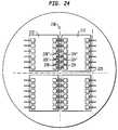
- FIG. 24is a bottom view of a variation of the stacked assembly illustrated in FIG. 21 .
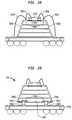
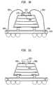
- FIGS. 25A and 25Bare illustrations of apparatus typically employed in the manufacture of stacked assemblies discussed herein.
- FIG. 26is a sectional view of a stacked assembly as attached to a circuit panel in accordance with an embodiment of the invention.
- FIG. 27is a sectional view of a stacked assembly as attached to a circuit panel in accordance with a variation of the embodiment illustrated in FIG. 26 .
- FIG. 28is a sectional view of a stacked assembly as attached to a circuit panel in accordance with another variation of the embodiment illustrated in FIG. 26 .
- FIG. 29is a sectional view of a stacked assembly as attached to a circuit panel in accordance with another embodiment of the invention.
- FIG. 30is a sectional view of a stacked assembly as attached to a circuit panel in accordance with a variation of the embodiment illustrated in FIG. 29 .
- FIG. 31is a sectional view of a stacked assembly as attached to a circuit panel in accordance with another variation of the embodiment illustrated in FIG. 29 .
- FIG. 32is a sectional view of a stacked assembly as attached to a circuit panel in accordance with another embodiment of the invention.
- FIGS. 1-4Billustrate a method and apparatus for stacking microelectronic components.
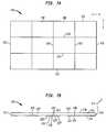
- a portion of a first wafer or subassembly 10includes a plurality of microelectronic elements 12 , each positioned side by side and adjacent to one another.
- the first wafer or subassembly 10preferably includes numerous rows of microelectronic elements 12 aligned along an X-axis and a Y-axis.
- the microelectronic elementsare formed integral with one another using conventional semiconductor process techniques.
- the subassembly 10may be a portion of a wafer.
- the broken lines in the FIG. 1Aillustrate that the subassembly may have additional elements attached thereto and may be in the shape of a circular wafer.
- Each microelectronic element 12includes a front face 14 and an oppositely-facing rear face 16 .
- the microelectronic elements 12also include first edges 18 , second edges 20 , third edges 19 and fourth edges 21 , all of which extend from the front faces 14 to the rear faces 16 of the microelectronic elements 12 .
- a first edge 18 of one microelectronic element 12is attached to a second edge 20 of a second and adjacent microelectronic element 12 .
- a third edge 19 of one microelectronic element 12is attached to a fourth edge 21 of an adjacent microelectronic element.
- the microelectronic elements 12 positioned within the middle of the first subassembly 10are bordered by an adjacent microelectronic element 12 at all four edges, as shown in FIG. 1A .
- the microelectronic elements 12 positioned at a first end 11 , a second end 13 , a third end 15 or a fourth end 17 of the waferhave at least one edge unencumbered by an additional microelectronic element.
- the edgesare depicted in the drawings for clarity of illustration, in practice the edges may not be visible. Rather, at this stage, the edges or strips where adjacent microelectronic elements 12 contact one another are saw lanes or strips where the wafer can be cut without damaging the individual microelectronic elements. For instance, as shown in FIG.
- first wafer/subassembly 10may include any number of microelectronic elements 12 including as little as two or as many as is desirable
- Each of the microelectronic elements 12also includes a plurality of contacts 22 exposed at the respective front face 14 of the microelectronic element 12 .
- a trace 24extends outwardly from each of the contacts 22 to a respective first, second, third or fourth edge 18 , 20 , 19 , and 21 of the individual microelectronic element 12 .
- trace 24 ′extends outwardly from contact 22 ′ towards the second edge 20 ′ of microelectronic element 12 ′.
- the trace 24 ′extends to and contacts trace 24 ′′, which extends outwardly from contact 22 ′′.
- traces 24 ′ and 24 ′′meet at the attachment point of microelectronic elements 12 ′ and 12 ′′ and may actually form a single trace extending between contact 22 ′ and contact 22 ′. However, it is not required that the traces actually contact one another. Similar structures may be included for all adjacent microelectronic elements 12 .
- contacts 22which are positioned at the respective ends of the first subassembly 10 do not have traces 24 that extend to an adjacent contact on a different microelectronic element, but rather these traces 24 simply extend to a respective end of the first assembly 10 .
- the first subassembly 10is positioned over a second wafer/subassembly 10 A and third wafer/subassembly 10 B.
- the second subassembly and third subassembly 10 A, 10 Bare similarly constructed to the first subassembly 10 and thus like elements will be given similar character references unless otherwise specified.
- the stacked assembly 30 of FIG. 2includes three individual wafers/subassemblies stacked one upon another, but in alternate embodiments the stacked assembly 30 may include less or more wafers/subassemblies positioned on top of each other.
- the microelectronic elements 12 of the first subassembly 10are aligned with the microelectronic elements 12 A of the second subassembly 10 A and the microelectronic elements 12 B of the third subassembly 10 B.
- the respective first, second, third and fourth edges of each of the microelectronic elements 12 , 12 A, 12 B of the respective subassemblies 10 , 10 A, 10 Bare also aligned along longitudinal axes. Therefore, the respective saw lanes 23 , 23 A and 23 B of each of the subassemblies are also aligned with one another.
- the stacked assembly 30consists of a plurality of microelectronic elements 12 , 12 A, 12 B, oriented and aligned in various rows and columns.
- an adhesive layer 32is positioned between the front face 14 of the first subassembly 10 and the rear face 16 A of the second subassembly 10 A.
- an adhesive layer 33is also positioned between the front face 14 A of the second subassembly 10 A and the rear face 16 B of the third subassembly 10 B.
- An additional adhesive layer 35may also be disposed on the front face 14 B of the third subassembly 10 B so as to protect the contacts 22 B and traces 24 B of the third subassembly 10 B.
- the adhesive layers 32 , 33 , 35may be formed from an epoxy or the like.
- the adhesive layers 32 , 33 , 35are allowed to cure such that the respective subassemblies 10 , 10 A, 10 B are adhered to one another and form stacked assembly 30 , which includes a plurality of microelectronic elements 12 , 12 A, 12 B stacked adjacent to and upon one another.
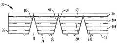
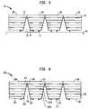
- a plurality of notches 46may be cut into the stacked assembly 30 .
- the notches 46are preferably formed using a mechanical cutting instrument not shown in the figures. Examples of such a mechanical cutting instrument can be found in U.S. Pat. Nos. 6,646,289 and 6,972,480, the disclosures of which are hereby incorporated by reference herein.
- the notches 46are cut from the stacked assembly 30 at locations that are proximate the respective first edges 18 , 18 A, 18 B, second edges 20 , 20 A and 20 B, third edges 19 , 19 A, 19 B and fourth edges 21 , 21 A, 21 B of the respective microelectronic elements 12 , 12 A, 12 B of the various subassemblies 10 , 10 A, 10 B.
- the notches 46are formed by cutting gaps 47 at the saw lanes 23 , 23 A and 23 B. Since the saw lanes 23 , 23 A and 23 B of each of the subassemblies 10 , 10 A 10 B are aligned throughout the stacked assembly 30 , a single cut may be used to form the gaps 47 between multiple subassemblies.
- the notches 46do not extend entirely through the stacked assembly 30 .
- the microelectronic elements 12 of the first subassembly 10remain attached to each other as the various notches 46 do not extend entirely through the first subassembly.
- the notches 46do extend far enough so as to intersect the traces 24 of the first subassembly 10 that extend between contacts 22 exposed at adjacent microelectronic elements 12 .
- the notches 46dissect not only the various adhesive layers 32 , 33 , 35 interconnecting the subassemblies 10 , 10 A, 10 B but also adjacent microelectronic elements 12 A, 12 B and respective traces 24 , 24 A, 24 B of each subassembly.
- the notches 46are illustrated having inclined side walls 48 , 50 , the side walls may also be straight.
- notch 46 A of FIG. 3intersects microelectronic element 52 and microelectronic element 54 of second subassembly 10 A.
- the notch 46 Aintersects the two microelectronic elements 52 , 54 such that the various edges of each of the microelectronic elements, which were previously attached to one another and formed saw lane 23 are separated by a gap 47 .
- the gap 47 created by the notch 46 Aexposes the traces 56 and 58 adjacent the notch 46 A.
- a similar structureis preferably included for all of the edges of the various microelectronic elements throughout the stacked assembly 30 .
- the exposed traces 24 , 24 A, 24 Bform contact surfaces for each of the microelectronic elements 12 , 12 A, 12 B.
- first edge 60 and second edge 62 of the stacked assembly 30does not have to be mechanically cut because the traces that extend toward these respective edges are already exposed.
- first and second edge 60 , 62may also be mechanically cut so as to create a more symmetrical configuration.
- the edges of the stacked assembly 30 not shown in the figuresalso do not have to be mechanically cut although it may be desirable.
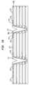
- leads 66may be formed on the inclined side walls 48 , 50 of notches 46 .
- the inclined side walls 48 , 50extend through at least part of the various first, second and third subassemblies, 10 , 10 A, 10 B, that were created as a result of the notches 46 , as shown in FIGS. 4A and 4B .
- the leads 66may be formed by any suitable metal deposition technique, for example, a process that includes sputtering, three-dimensional lithography and electroplating. Additional processes may also be employed. One such process is disclosed in U.S. Pat. No. 5,716,759, the disclosure of which is hereby incorporated by reference herein.
- the leads 66extend within the various notches 46 , and establish electrical contact with the traces 24 , 24 A and 24 B.
- the leads 66extend past the inclined side walls 48 , 50 of notches 46 and are exposed at a first surface 70 of the adhesive layer 35 positioned below the third subassembly 10 B. Therefore, the leads 66 include ends 75 remote from notches 46 and exposed on the surface of adhesive layer 35 . Pads or solder bumps 74 may be formed at the ends 75 of the leads 66 .
- Each lead 66is in contact with three traces 24 , 24 A, 24 B as a result of the traces being aligned and exposed at a respective inclined side wall 48 or 50 .
- the leads 66may be in electrical connection with only one or two of the traces 24 , 24 A, 24 B at a respective inclined side wall 48 or 50 .
- Such an orientationmay be as a result of the positioning of the traces 24 , 24 A, 24 B in different planes that are into and out of the page as viewed by the reader.
- trace 24 illustrated in FIG. 4Bmay be offset from trace 24 A so that trace 24 is closer to the reader if viewing in a three-dimensional orientation.
- the lead 66which is aligned with trace 24 , is also offset from trace 24 A and not in contact with trace 24 A. So although in a two-dimensional view, the traces 24 , 24 A may appear to be attached to lead 66 in FIG. 4B , only one may be actually attached to the lead.
- individual packages 80may be created by mechanically cutting through the wafer 10 of microelectronic elements 12 of the first subassembly 10 .
- the microelectronic elements 12 of the first subassembly 10are cut at locations that are proximate the notches 46 such that the notches 46 are allowed to extend entirely through the stacked assembly 30 .
- a plurality of stacked individual units 80are created, with each stacked individual unit 80 containing a plurality of microelectronic elements stacked one upon another.
- the stacked individual units 80may be electrically connected to a microelectronic element such as a substrate 83 , circuit board or circuit panel via the solder bumps 74 , as shown in FIG. 5 .
- the stacked individual unit 80may be incorporated into microprocessors and RF units among other assemblies but may be particularly adaptable for Flash Memory and DRAM units.
- the stacked assembly 130may include an additional substrate such as packaging layer 180 .
- Stacked assembly 130is similarly constructed to stacked assembly 30 discussed previously with regard to FIGS. 1-5 and includes most if not all of the same features discussed with regard to stacked assembly 30 .
- stacked assembly 130may be constructed following steps previously discussed with regard to stacked assembly 30 .
- the only addition to stacked assembly 130 as compared to stacked assembly 30is that during the manufacture of the stacked assembly 130 and preferably prior to creating notches in the stacked assembly 130 , a packaging layer 180 is positioned below compliant layer 135 .
- the packaging layer 180is preferably formed of glass, silicon or a similar material.
- a plurality of notches 146are formed using a cutting instrument, as discussed with regard to stacked assembly 30 . This exposes traces 124 , 124 A, 124 B at the inclined side walls, 148 , 150 of the notches 146 . Further, a plurality of leads 166 may then be created on the inclined side walls 148 , 150 and be placed in electrical contact with the various traces 124 , 124 A, 124 B exposed at the inclined side walls, 148 , 150 of the notches 146 as discussed with regard to stacked assembly 30 . The various leads 166 preferably extend beyond the notches 146 and onto a front surface 182 of the packaging layer 180 .
- Exposed ends 175 of the leads 166may include pads or solder bumps 174 .
- the notchesmay be extended through the row of microelectronic elements 112 of the first subassembly 110 so as to create individual stacked units 180 .
- the stacked assembly 230may include an additional substrate such as packaging layer 201 .
- Stacked assembly 230is similarly constructed to stacked assemblies 30 and 130 discussed previously with regard to FIGS. 1-7 , except that the assembly starts with substrate layer 201 , and includes many of the same features discussed with regard to stacked assembly 30 and 130 .
- stacked assembly 230may be constructed following steps previously discussed with regard to stacked assemblies 30 and 230 .
- a portion of a first wafer or subassembly 210includes a plurality of microelectronic elements 212 , each positioned side by side and adjacent to one another.
- the first wafer or subassembly 210preferably includes numerous rows of microelectronic elements 212 aligned along an X-axis and a Y-axis.
- the microelectronic elementsare formed integral with one another using conventional semiconductor process techniques. It should be apparent that the subassembly 210 may be a portion of a wafer and that the various components are replicated repeatedly over the extent of the wafer.
- the FIGS. 7A-7Cillustrate that the subassembly may have additional elements attached thereto and may be in the shape of a circular wafer.
- Each microelectronic element 212includes a front face 214 and an oppositely-facing rear face 216 .
- the microelectronic elements 212also include first edges 218 , second edges 220 , third edges 219 and fourth edges 221 , all of which extend from the front faces 214 to the rear faces 216 of the microelectronic elements 212 .
- a first edge 218 of one microelectronic element 212is attached to a second edge 220 of a second and adjacent microelectronic element 212 .
- a third edge 219 of one microelectronic element 212is attached to a fourth edge 221 of an adjacent microelectronic element.
- the microelectronic elements 212 positioned within the middle of the first subassembly 210are bordered by an adjacent microelectronic element 212 at all four edges, as shown in FIG. 7A .
- the microelectronic elements 212 positioned at a first end 211 , a second end 213 , a third end 215 or a fourth end 217 of the waferhave at least one edge unencumbered by an additional microelectronic element.
- the edgesare depicted in the drawings for clarity of illustration, in practice the edges may not be visible. Rather, at this stage the edges or strips where adjacent microelectronic elements 212 contact one another are saw lanes or strips where the wafer can be cut without damaging the individual microelectronic elements.
- first wafer/subassembly 210may include any number of microelectronic elements 212 including as little as two or as many as are desirable.
- Each of the microelectronic elements 212also includes a plurality of contacts 222 exposed at the respective front face 14 of the microelectronic element 212 best seen in FIG. 7C . Further, a trace 224 extends outwardly from each of the contacts 222 to respective edges 218 , 220 , 219 , and 221 of the individual microelectronic element 212 .
- the traces 224may meet at the attachment point of microelectronic elements 212 ′ and 212 ′′ and may actually form a single trace extending between contact 222 ′ and contact 222 ′′. However, it is not required that the traces actually contact one another. Similar structures may be included for all adjacent microelectronic elements 212 .
- contacts 222which are positioned at the respective ends of the first subassembly 210 do not have traces 224 that extend to an adjacent contact on a different microelectronic element, but rather these traces 224 simply extend to a respective end of the first assembly 210 .
- FIGS. 7-22In contrast to the embodiments discussed in connection with FIGS. 1-6 , the embodiment of FIGS. 7-22 is shown constructed in stacked fashion from the substrate upwards. Consequently, many of the various components and processes are depicted in inverted fashion related to the earlier figures.
- FIG. 8A packaging support wafer or layer 201 with substrate 202 for the stacked assembly of this embodiment is shown in FIG. 8 .
- the substrate 202is preferably formed of glass, silicon or a similar material that provides sufficient mechanical strength to support and reinforce the subsequent layers of the stacked assembly. For this reason, the substrate 202 may be thicker than the subsequent layers.
- the substrate layer 202 materialmay also be thinned or even removed during later process steps by etching or mechanically polishing when support is no longer needed.
- the substratehas a lower surface 205 and an upper surface 206 and extends to a leftward side 203 and rightward surface 204 . Depicted in FIG. 9 are a plurality of relief cavities 208 and 208 ′ created in the upper surface 206 .
- cavities 208are aligned with the anticipated positions of saw lanes for severing the stacked packages.
- the cavities 208 , 208 ′are created by mechanical cutting instruments as described above for the stacked assemblies 30 and 130 .
- the relief cavities 208 , 208 ′function as a stress relief to prevent fracture of the stacked assemblies due to notching of the substrate 202 during subsequent operations. Consequently, the cavities 208 are preferably formed with corner radii to alleviate stress concentrations.
- an adhesive layer 209is applied to the upper surface 206 and the cavities 208 , 208 ′ as shown in FIG. 10 .
- the adhesive layerhas a thickness over the upper surface 206 of 2.5-4.0 micrometers.
- the first subassembly 212is positioned over the substrate layer 201 .
- the contacts 222 , 222 ′ and traces 224 , 224 ′are aligned with the respective cavities 208 , 208 ′ and thus saw lanes 218 and 222 .
- the active lower surface 214 and the traces 224 and 224 ′are applied to the adhesive layer 209 of the substrate layer 201 and the adhesive is cured.
- the subassembly 210including the traces 224 and 224 ′ are bonded to and supported by the substrate layer 201 .
- the upper surface 216 of the subassembly 210may be thinned to create a new surface 216 ′ and reduce the height of the subassembly as shown in FIG. 12 .
- the reduced height of the subassemblyis 22.4-25.4 micrometers if a compact stacked package is desired.
- a plurality of initial notches 240 , 240 ′may be formed into the subassembly 210 to expose the traces 224 , 224 ′.
- the notches 240 , 240 ′are preferably formed using non-mechanical techniques such as selective chemical etching in order to preserve the delicate traces 240 , 240 ′.
- the traces 240 , 240 ′are adhered to and supported by the adhesive 209 of the substrate 201 during this step.
- the initial notches 240 , 240 ′are aligned with the contacts 222 , 222 ′, the traces 224 , 224 ′ the cavities 208 , 208 ′ and saw lanes 218 and 222 .
- the profile of the initial notches 40 , 41is configured to provide clearance for later notches as will be described.
- an adhesive layer 243is applied to the upper surface 216 or 216 ′ and the initial notches 40 , 40 ′, as shown in FIG. 14 .
- the adhesive layerhas a thickness over the upper surface 216 or 216 ′ of approximately 2.5-4.0 micrometers.
- second, third and fourth subassembliesare aligned with subassembly 210 , stacked and laminated sequentially upward from subassembly 210 and substrate layer 201 .
- the same sequence of steps earlier followed to laminate subassembly 210 to substrate 201is used to laminate each of subassemblies 210 A, 210 B and 210 C.
- the steps including alignment, lamination, curing, thinning, creation of initial notches and application of adhesiveare followed sequentially for each step to create the stacked assembly 230 .
- microelectronic elements 212 of the first subassembly 210are aligned with the microelectronic elements 212 A of the second subassembly 210 A, the microelectronic elements 212 B of the third subassembly 210 B, and the microelectronic elements 212 C of the third subassembly 210 C.
- the initial notches 240 , 240 ′, 240 A, 240 A′, 240 B, 240 B′, 240 C, 240 C′are respectively aligned with the contacts 222 , 222 ′, 222 A, 222 A′, 222 B, 222 B′, 222 C, 222 C′, the traces 224 , 224 ′, 224 A, 224 A′, 224 B, 224 B′, 224 C, 224 C′, the cavities 208 , 208 ′ and the saw lanes 218 and 222 .
- the stacked assembly 230consists of a plurality of stacked and adhered microelectronic elements 12 , 12 A, 12 B, 12 C oriented and aligned in various rows and columns.
- the notches 246are cut from the stacked assembly 230 at locations that are proximate the respective first edges 218 , 218 A, 218 B, and 218 C, second edges 220 , 220 A, 220 B and 220 C, third edges 219 , 219 A, 219 B, 219 C and fourth edges 221 , 221 A, 221 B, 221 C of the respective microelectronic elements 12 , 12 A, 12 B, 12 C of the various subassemblies 10 , 10 A, 10 B, 10 C.
- the notches 246 , 247are formed at the saw lanes 220 , 218 by the methods described for the earlier embodiments. As seen in FIG.
- the plurality of notches 246are cut through the adhesive layers 243 , 243 A, 243 B, 243 C.
- the notches 246do not extend entirely through the stacked assembly 230 but rather extend only partially into the relief cavities 208 , 208 ′.
- the substrate 202remains intact to connect the stacked microelectronic elements and is protected from cracking because the adhesive 209 rather that the substrate is cut.
- the notches 246are illustrated having inclined side walls 248 , 250 , the side walls may also be straight.
- the stacked assembly 230 of FIG. 17includes four individual wafers/subassemblies stacked one upon another, but in alternate embodiments the stacked assembly 230 may include less or more wafers/subassemblies positioned on top of each other. Also shown in FIG. 17 is an optional thinning of the substrate 202 which may be accomplished by mechanical polishing or etching. This step may be performed between various steps in the process, preferably after formation of the notches 246 .
- leads 266may be formed on the inclined side walls 248 , 250 of notches 246 .
- the inclined side walls 248 , 250extend through at least part of the various first, second, third and fourth subassemblies 210 , 210 A, 210 B, 210 C that were created as a result of the notches 246 , as shown in FIGS. 17 and 18 .
- the leads 266may be formed by any suitable metal deposition technique as described for the previous embodiments.
- the leads 266extend within the various notches 246 , and establish electrical contact with the traces 224 , 224 A, 224 B and 224 C.
- the leads 266extend past the inclined side walls 248 , 250 of notches 246 and are adhered to the adhesive layer 243 C on the upper surface 216 C′ of the third subassembly 210 C. Therefore, the leads 266 include ends 275 remote from notches 246 and exposed on the surface of adhesive layer 243 C.
- Each lead 266is in contact with four traces 224 , 224 A, 224 B, 224 C as a result of the traces being aligned and exposed at respective inclined side walls 248 or 250 .
- the leads 266may be in electrical connection with less than four of the traces 224 , 224 A, 224 B, 24 C at a respective inclined side wall 48 or 50 .
- Such an orientationmay be as a result of the positioning of the traces 224 , 224 A, 224 B, 224 C in different planes that are into and out of the page as viewed by the reader as discussed for the previous embodiments.
- Pads or solder bumpsmay be formed at the ends 275 of the leads 266 .
- solder mask 277may be patterned over the surface of adhesive layer 216 C and leads 266 as shown in FIG. 19 for the attachment of wires or solder bumps.
- leads 266may be extended to the bottom surface of the substrate 202 .
- the leads 266extend past the inclined side walls 248 , 250 of notches 246 and enter the adhesive layer 209 within the relief cavity 208 positioned below the first subassembly 210 .
- the bottom of leads 266are exposed and the leads may be extended by the methods previously discussed to create bottom leads 286 .
- Solder mask 227may be patterned over the bottom surface of substrate 202 for the attachment of wires or solder bumps to allow the formation of pads or bumps at the ends 288 .
- a particular advantage of this arrangementis that either stacked assemblies 230 or individual packages may in turn be stacked and electrically interconnected, one upon the other by aligning and connecting using, for instance solder bumps, the respective top ends 275 and bottom ends 288 .
- the top ends 275 and bottom ends 288 to be connectedare align in an appropriate pattern in the x-y plane to allow interconnection.
- leads 266allow testing probes to access the elements, defective subassembly layers may be detected and isolated to allow sorting and rework. Higher-level integration as well as wafer level rework is facilitated by the ability to stack assemblies 230 .
- leads disposed at a bottom surface of a unit as illustrated in FIG. 20may be connected to leads provided at a top surface of an adjacent unit through conductive masses, e.g., spheres or bumps of conductive material, e.g., solder. While having a greater overall thickness, elements from such stacked stack assemblies are functionally repaired to be equivalent to a non-defective stack assembly 230 and the value of the functioning layers 210 may be economically recovered by wafer level rework.
- individual packages 280may be created by mechanically cutting through the leads 266 , the adhesive 209 and the substrate 202 , to sever the packages. The cut are aligned with dicing lanes 218 and 220 at locations that are proximate the notches 246 such that the notches 246 are allowed to extend entirely through the stacked assembly 230 .
- a plurality of stacked individual elements 280are created, with each stacked individual unit 280 containing a plurality of microelectronic elements stacked one upon another.
- the stacked individual units 280 as shown in FIG. 22may be electrically connected to a microelectronic element such as a substrate, circuit board or circuit panel via wire bonding or via pads 275 or the solder bumps 274 , as shown in FIG. 23 .
- three stacked assemblies 230 of the type shown in FIG. 20 or FIG. 21may be stacked and interconnected.
- Bond wires 2202 , 2202 ′, 2202 ′′ connecting lands 2204 , 2204 ′ and 2204 ′′ of the stacked assembliesprovide interconnection to terminals 2206 of a circuit panel 2210 .
- the bond wiresmay be arranged to connect lands of adjacent levels as shown in FIG. 20A or each bond wire may directly connect a stacked assembly to the circuit panel. Alternatively, some of the bond wires connected to a particular stacked assembly may be connected to another stacked assembly which is not adjacent to the particular stacked assembly.
- a face 2220 ′′ of a stacked assembly 230 ′′ and a land 2204 ′′ thereonextends beyond a face 2220 ′ and an edge 2222 ′ of stacked assembly 230 ′ and a land 2204 ′ thereon, thus permitting the lands 2204 ′ and 2204 ′′ to be interconnected using bond wire 2202 ′.
- a face 2220 ′ of the stacked assembly 230 ′ and the land 2204 ′ thereonextends beyond a face 2220 and an edge 2222 of stacked assembly 230 and a land 2204 thereon, thus permitting the lands 2204 ′ and 2204 to be interconnected using bond wire 2202 .
- FIGS. 7-23result in thin elements 280 produced by wafer level packaging. Because the individual layers can be fabricated with thickness of approximately 25 micrometers, a total die package using a 30 micrometer substrate can be no less than 155 micrometers thick. As described, the substrate can be further thinned to reduce the package thickness to less than 125 micrometers.
- notches 246are formed in the stacked assembly 230 ( FIG. 17 ).
- the notchestypically extend along edges of each microelectronic element 212 , 212 ′ aligned with saw lanes 218 , 220 , etc., such that a series of traces 224 ( FIG. 7C ) of each microelectronic element are exposed within the notches at the edges.
- the notchesmay extend the entire length of the respective saw lanes of the stacked assembly 230 or may be a series of openings each extending a part of the length of the respective saw lane to which the opening is aligned. As depicted in FIG.
- all of the traces 224 extending from contacts 222 ′′ of microelectronic element 212 and all of the traces 224 extending from contacts 222 ′ of microelectronic element 212 ′may be exposed within one notch 246 ( FIG. 17 ).
- Leads 266( FIG. 18 ) may then be formed by depositing a primary metal layer, e.g., by sputtering, electroless deposition, etc., along edges of the subassemblies 210 exposed within the notches.
- the primary metal layercan then be photolithographically patterned into separate leads, followed by electroplating to increase the thickness of leads and if desired, form leads having multiple different metal layers.
- openings 228 , 228 ′, 228 ′′are formed in alignment with the saw lanes 218 , 220 , etc.
- the notches 246FIG.
- each of the openings 228 , 228 ′, 228 ′′, etc.exposes no more than a single trace 224 , 224 ′, 224 ′′ of each respective microelectronic element.
- traces 224 connected to contacts of adjacent microelectronic elements 212 , 212 ′are exposed within an opening 228 .
- traces 224 ′ connected to contacts of the adjacent microelectronic elementsare exposed within another 228 ′ of the openings
- traces 224 connected to contacts of the adjacent microelectronic elementsare exposed within another 228 ′′ of the openings.
- respective traces 224 connected to microelectronic elements of the stacked subassembliesmay be exposed within a single opening, but no more than one trace of each microelectronic element is exposed within each opening.
- all openings 228 , 228 ′, 228 ′′, etc., in the stacked assemblycan be simultaneously filled with a conductor to form conductive vias connected to single traces of each microelectronic element.
- the openingscan be filled with a metal to form conductive vias by depositing a primary metal, e.g., by sputtering or electroless deposition, and then electroplating the resulting structure. Metal remaining from the electroplating step which lies above the surface of the exposed adhesive or dielectric layer 243 C. ( FIG.
- the resulting metal layer overlying the uppermost adhesive layer 243 Ccan be patterned by photolithography into individual leads 266 ( FIG. 18 ) extending from the vias over layer 243 C. Conductive bumps may then be formed at ends of the leads, as shown and described above with reference to FIG. 23 .
- FIGS. 25A and 25Bare illustrations of apparatus employed in the manufacture of assemblies of the types discussed herein.
- a conventional wafer fabrication facility 680provides complete wafers 681 , of the type partially shown in FIGS. 1A and 1B .
- Individual wafers 682are bonded on their active surfaces to protective layers 683 by bonding apparatus 685 , preferably having facilities for rotation of the wafer 682 , the layer 683 and epoxy so as to obtain even distribution of the epoxy.
- the bonded wafer 686is thinned at its non-active surface as by grinding apparatus 684 using an abrasive 687 .
- the waferis then etched at its non-active surface, preferably by photolithography, such as by using conventional spin-coated photoresist, using a mask exposure machine 692 for the exposure of light sensitive photoresist 690 through the mask 691 and later etching the silicon in a bath 693 using solution 699 .
- the etched waferis bonded on the non-active side to protective layer 686 by bonding apparatus 694 , which may be essentially the same as apparatus 685 , to produce a doubly bonded wafer sandwich.
- the wafermay then by bonded to a second or more wafers.
- Notching apparatus 695partially cuts the bonded wafers in a method of forming a stacked package as described above with reference to FIGS. 1-6 .
- the notched wafersare then subjected to anti-corrosion treatment in a bath 696 , containing a chromating solution 698 .
- a chemical etching apparatus(not shown) may be used to form notches exposing one or more traces or openings exposing single traces of respective microelectronic elements in accordance with the methods of fabrication described above with respect to FIGS. 7-24 .
- Conductive layer deposition apparatus 700which operates by vacuum deposition techniques, is employed to produce a conductive layer on one or more surfaces of each die of the wafers.
- the conductive layer deposition apparatus 700may be employed prior to the two wafers being assembled together.
- Configuration of the contact strips or lead bridgesis carried out preferably by using conventional electro-deposited photoresist 701 .
- the photoresist 701is applied to the stacked wafers 707 in a photoresist bath assembly 702 .
- the photoresist 701is preferably light configured by a UV exposure system 704 , which may be identical to system 692 , using a mask 705 to define suitable etching patterns.
- the photoresistis then developed in a development bath 706 , and then the wafer is etched in a metal solution 708 located in an etching bath 710 , thus providing a conductor configuration.
- the exposed conductive stripsare then plated, preferably by electroless plating apparatus 712 .
- the stacked wafersare then diced into individual prepackaged integrated devices.
- the dicing blade 714should be a diamond resinoid blade of thickness 4-12 mils, which corresponds to the thickness of the saw lanes.
- a stacked assembly 280( FIG. 22 ) is shown having a rear face 2602 attached, e.g., by way of an adhesive (not shown), to an interconnection element 2610 or circuit panel.
- Bond wires 2604electrically connect ends 2668 of leads 2666 to contacts 2606 on an inner face 2601 of an interconnection element 2610 .
- the contacts 2606are connected by way of vias 2608 to conductive bumps or balls 2612 , e.g., solder balls exposed at an outer face 2611 of the interconnection element.
- conductive bumps or balls 2612e.g., solder balls exposed at an outer face 2611 of the interconnection element.
- a microelectronic elemente.g., a semiconductor chip
- leads 2666extending above a front face 2622 of a microelectronic element 210 of the stacked assembly 280 through conductive masses 2624 , e.g., solder balls, among others.
- microelectronic elements 210 included in the stacked assemblyinclude memory devices, including, without limitation, dynamic random access memories (“DRAMs”), static random access memories (“SRAMs”), erasable programmable read only memories (“EPROMs”), e.g., such memories which can be erased via exposure to radiation or which can be erased and reprogrammed via electrical means, or flash memory, which is a form of nonvolatile random access memory in which data can be stored, altered and overwritten without having to reprogram the chip.
- DRAMsdynamic random access memories
- SRAMsstatic random access memories
- EPROMserasable programmable read only memories
- flash memorywhich is a form of nonvolatile random access memory in which data can be stored, altered and overwritten without having to reprogram the chip.
- the chip 2620includes a processor, e.g., microprocessor or microcontroller element, among others, the processor capable of accessing and executing a program in connection with use of the memory resources contained in the stacked assembly 280 .
- the chip 2620may contain circuitry which matches that of one or more of the microelectronic elements 210 in function or circuitry. In such case, chip 2620 can serve as a replacement unit connected by way of leads 2666 to other microelectronic elements 210 , the chip 2620 connected by way of bond wires 2604 to the interconnection element.
- leads extending from that defective microelectronic elementcan be electrically disconnected from contacts at the front face 2622 , e.g., by mechanical or laser techniques.
- electrically fusible elementse.g., electrical fuses or antifuses
- the repair chip 2620can be electrically connected in place of the defective chip of the stacked assembly.
- FIG. 27illustrates a variation of the embodiment illustrated in FIG. 26 , wherein a chip 2720 is mounted with a front face 2722 thereof facing away from the front face 2622 of the adjacent microelectronic element 210 .
- Bond wires 2704connect pads 2716 of the chip to contacts 2706 of the interconnection element.
- bond wires 2804 connected to the pads 2704 of the chip 2720are connected to exposed contacts 2806 on the stacked assembly.
- the exposed contacts 2806may be connected to one or more of the microelectronic elements of the stacked assembly by way of leads 2666 . Alternatively, or in addition thereto, the exposed contacts 2806 may be connected to the interconnection element by way of other bond wires 2814 .
- FIG. 29illustrates a variation of the embodiment shown in FIG. 29 , in which a chip 2720 mounted to the front face 3001 of the stacked assembly is electrically connected directly to the interconnection element 3010 by way of bond wires 3004 which extend from pads on the chip 2720 to contacts 3006 of the interconnection element.
- FIG. 30illustrates a variation of the embodiment shown in FIG. 29 , in which a chip 2720 mounted to the front face 3001 of the stacked assembly is electrically connected directly to the interconnection element 3010 by way of bond wires 3004 which extend from pads on the chip 2720 to contacts 3006 of the interconnection element.
- a chip 2620is flip-chip mounted to ends of leads 2666 or other contacts exposed at the front face 3001 of the stacked assembly.
- a stacked assembly 280is flip-chip mounted to an interconnection element 2610 , with the front face 3201 of the stacked assembly confronting a front face 2601 of the interconnection element.
Landscapes
- Engineering & Computer Science (AREA)
- Microelectronics & Electronic Packaging (AREA)
- Power Engineering (AREA)
- Physics & Mathematics (AREA)
- Condensed Matter Physics & Semiconductors (AREA)
- General Physics & Mathematics (AREA)
- Computer Hardware Design (AREA)
- Manufacturing & Machinery (AREA)
- Wire Bonding (AREA)
- Packaging Frangible Articles (AREA)
Abstract
Description
Claims (8)
Priority Applications (15)
| Application Number | Priority Date | Filing Date | Title |
|---|---|---|---|
| US11/787,209US7829438B2 (en) | 2006-10-10 | 2007-04-13 | Edge connect wafer level stacking |
| CN201110370722.2ACN102386173B (en) | 2006-10-10 | 2007-10-09 | Edge connects wafer level stacking microelectronics Packaging and manufacture method thereof |
| CN2007800455429ACN101553923B (en) | 2006-10-10 | 2007-10-09 | Edge-connected wafer-level stacked microelectronic package and method of manufacturing the same |
| JP2009532373AJP5114490B2 (en) | 2006-10-10 | 2007-10-09 | Edge connected wafer level laminate |
| PCT/US2007/021552WO2008045422A2 (en) | 2006-10-10 | 2007-10-09 | Edge connect wafer level stacking |
| KR1020097009468AKR101433777B1 (en) | 2006-10-10 | 2007-10-09 | A stacked microelectronic package and its manufacturing method, an assembly including the package, and a stacked microelectronic assembly |
| US12/143,743US7901989B2 (en) | 2006-10-10 | 2008-06-20 | Reconstituted wafer level stacking |
| US12/908,265US8022527B2 (en) | 2006-10-10 | 2010-10-20 | Edge connect wafer level stacking |
| US12/941,392US8076788B2 (en) | 2006-10-10 | 2010-11-08 | Off-chip vias in stacked chips |
| US13/086,645US8426957B2 (en) | 2006-10-10 | 2011-04-14 | Edge connect wafer level stacking |
| US13/316,890US8476774B2 (en) | 2006-10-10 | 2011-12-12 | Off-chip VIAS in stacked chips |
| US13/369,846US8461673B2 (en) | 2006-10-10 | 2012-02-09 | Edge connect wafer level stacking |
| JP2012225973AJP5422720B2 (en) | 2006-10-10 | 2012-10-11 | Edge connected wafer level laminate |
| US13/914,896US9048234B2 (en) | 2006-10-10 | 2013-06-11 | Off-chip vias in stacked chips |
| US14/725,975US9899353B2 (en) | 2006-10-10 | 2015-05-29 | Off-chip vias in stacked chips |
Applications Claiming Priority (3)
| Application Number | Priority Date | Filing Date | Title |
|---|---|---|---|
| US85085006P | 2006-10-10 | 2006-10-10 | |
| US11/704,713US8513789B2 (en) | 2006-10-10 | 2007-02-09 | Edge connect wafer level stacking with leads extending along edges |
| US11/787,209US7829438B2 (en) | 2006-10-10 | 2007-04-13 | Edge connect wafer level stacking |
Related Parent Applications (1)
| Application Number | Title | Priority Date | Filing Date |
|---|---|---|---|
| US11/704,713Continuation-In-PartUS8513789B2 (en) | 2006-10-10 | 2007-02-09 | Edge connect wafer level stacking with leads extending along edges |
Related Child Applications (2)
| Application Number | Title | Priority Date | Filing Date |
|---|---|---|---|
| US12/143,743Continuation-In-PartUS7901989B2 (en) | 2006-10-10 | 2008-06-20 | Reconstituted wafer level stacking |
| US12/908,265DivisionUS8022527B2 (en) | 2006-10-10 | 2010-10-20 | Edge connect wafer level stacking |
Publications (2)
| Publication Number | Publication Date |
|---|---|
| US20080083977A1 US20080083977A1 (en) | 2008-04-10 |
| US7829438B2true US7829438B2 (en) | 2010-11-09 |
Family
ID=38870245
Family Applications (4)
| Application Number | Title | Priority Date | Filing Date |
|---|---|---|---|
| US11/787,209Active2027-03-09US7829438B2 (en) | 2006-10-10 | 2007-04-13 | Edge connect wafer level stacking |
| US12/908,265ActiveUS8022527B2 (en) | 2006-10-10 | 2010-10-20 | Edge connect wafer level stacking |
| US13/086,645Expired - Fee RelatedUS8426957B2 (en) | 2006-10-10 | 2011-04-14 | Edge connect wafer level stacking |
| US13/369,846Expired - Fee RelatedUS8461673B2 (en) | 2006-10-10 | 2012-02-09 | Edge connect wafer level stacking |
Family Applications After (3)
| Application Number | Title | Priority Date | Filing Date |
|---|---|---|---|
| US12/908,265ActiveUS8022527B2 (en) | 2006-10-10 | 2010-10-20 | Edge connect wafer level stacking |
| US13/086,645Expired - Fee RelatedUS8426957B2 (en) | 2006-10-10 | 2011-04-14 | Edge connect wafer level stacking |
| US13/369,846Expired - Fee RelatedUS8461673B2 (en) | 2006-10-10 | 2012-02-09 | Edge connect wafer level stacking |
Country Status (5)
| Country | Link |
|---|---|
| US (4) | US7829438B2 (en) |
| JP (2) | JP5114490B2 (en) |
| KR (1) | KR101433777B1 (en) |
| CN (2) | CN102386173B (en) |
| WO (1) | WO2008045422A2 (en) |
Cited By (30)
| Publication number | Priority date | Publication date | Assignee | Title |
|---|---|---|---|---|
| US20100270679A1 (en)* | 2006-10-17 | 2010-10-28 | Tessera, Inc. | Microelectronic packages fabricated at the wafer level and methods therefor |
| US20110006432A1 (en)* | 2007-07-27 | 2011-01-13 | Tessera, Inc. | Reconstituted wafer stack packaging with after-applied pad extensions |
| US20110079903A1 (en)* | 2009-10-07 | 2011-04-07 | Chien-Hung Liu | Chip package and fabrication method thereof |
| US20110221053A1 (en)* | 2010-03-11 | 2011-09-15 | Qualcomm Incorporated | Pre-processing to reduce wafer level warpage |
| US8314501B2 (en)* | 2011-02-14 | 2012-11-20 | United Microelectronics Corp. | Semiconductor chip package structure, semiconductor chip and semiconductor chip group |
| US8349654B2 (en) | 2006-12-28 | 2013-01-08 | Tessera, Inc. | Method of fabricating stacked packages with bridging traces |
| US8426957B2 (en) | 2006-10-10 | 2013-04-23 | Tessera, Inc. | Edge connect wafer level stacking |
| US8431435B2 (en) | 2006-10-10 | 2013-04-30 | Tessera, Inc. | Edge connect wafer level stacking |
| US8466542B2 (en) | 2009-03-13 | 2013-06-18 | Tessera, Inc. | Stacked microelectronic assemblies having vias extending through bond pads |
| US8476774B2 (en) | 2006-10-10 | 2013-07-02 | Tessera, Inc. | Off-chip VIAS in stacked chips |
| US8513794B2 (en) | 2007-08-09 | 2013-08-20 | Tessera, Inc. | Stacked assembly including plurality of stacked microelectronic elements |
| US8551815B2 (en) | 2007-08-03 | 2013-10-08 | Tessera, Inc. | Stack packages using reconstituted wafers |
| US8629543B2 (en) | 2007-06-11 | 2014-01-14 | Invensas Corporation | Electrically interconnected stacked die assemblies |
| US8680662B2 (en) | 2008-06-16 | 2014-03-25 | Tessera, Inc. | Wafer level edge stacking |
| US8680687B2 (en) | 2009-06-26 | 2014-03-25 | Invensas Corporation | Electrical interconnect for die stacked in zig-zag configuration |
| US8704379B2 (en) | 2007-09-10 | 2014-04-22 | Invensas Corporation | Semiconductor die mount by conformal die coating |
| US8729690B2 (en) | 2004-04-13 | 2014-05-20 | Invensas Corporation | Assembly having stacked die mounted on substrate |
| US8884403B2 (en) | 2008-06-19 | 2014-11-11 | Iinvensas Corporation | Semiconductor die array structure |
| US8912661B2 (en) | 2009-11-04 | 2014-12-16 | Invensas Corporation | Stacked die assembly having reduced stress electrical interconnects |
| US9147583B2 (en) | 2009-10-27 | 2015-09-29 | Invensas Corporation | Selective die electrical insulation by additive process |
| US9153517B2 (en) | 2008-05-20 | 2015-10-06 | Invensas Corporation | Electrical connector between die pad and z-interconnect for stacked die assemblies |
| US9305862B2 (en) | 2008-03-12 | 2016-04-05 | Invensas Corporation | Support mounted electrically interconnected die assembly |
| US9490195B1 (en) | 2015-07-17 | 2016-11-08 | Invensas Corporation | Wafer-level flipped die stacks with leadframes or metal foil interconnects |
| US9508691B1 (en) | 2015-12-16 | 2016-11-29 | Invensas Corporation | Flipped die stacks with multiple rows of leadframe interconnects |
| US20170062399A1 (en)* | 2015-08-24 | 2017-03-02 | Globalfoundries Inc. | Method and structure for low-k face-to-face bonded wafer dicing |
| US9595511B1 (en) | 2016-05-12 | 2017-03-14 | Invensas Corporation | Microelectronic packages and assemblies with improved flyby signaling operation |
| US9728524B1 (en) | 2016-06-30 | 2017-08-08 | Invensas Corporation | Enhanced density assembly having microelectronic packages mounted at substantial angle to board |
| US9825002B2 (en) | 2015-07-17 | 2017-11-21 | Invensas Corporation | Flipped die stack |
| US9871019B2 (en) | 2015-07-17 | 2018-01-16 | Invensas Corporation | Flipped die stack assemblies with leadframe interconnects |
| US10566310B2 (en) | 2016-04-11 | 2020-02-18 | Invensas Corporation | Microelectronic packages having stacked die and wire bond interconnects |
Families Citing this family (51)
| Publication number | Priority date | Publication date | Assignee | Title |
|---|---|---|---|---|
| US7691668B2 (en)* | 2006-12-19 | 2010-04-06 | Spansion Llc | Method and apparatus for multi-chip packaging |
| US8198716B2 (en)* | 2007-03-26 | 2012-06-12 | Intel Corporation | Die backside wire bond technology for single or stacked die package |
| US8110930B2 (en)* | 2007-06-19 | 2012-02-07 | Intel Corporation | Die backside metallization and surface activated bonding for stacked die packages |
| US7880309B2 (en)* | 2007-07-30 | 2011-02-01 | Qimonda Ag | Arrangement of stacked integrated circuit dice having a direct electrical connection |
| US8044497B2 (en)* | 2007-09-10 | 2011-10-25 | Intel Corporation | Stacked die package |
| US8679861B2 (en)* | 2007-11-29 | 2014-03-25 | International Business Machines Corporation | Semiconductor chip repair by stacking of a base semiconductor chip and a repair semiconductor chip |
| JP2009193982A (en)* | 2008-02-12 | 2009-08-27 | Disco Abrasive Syst Ltd | Semiconductor device and manufacturing method of semiconductor device |
| US7846772B2 (en)* | 2008-06-23 | 2010-12-07 | Headway Technologies, Inc. | Layered chip package and method of manufacturing same |
| KR100997787B1 (en)* | 2008-06-30 | 2010-12-02 | 주식회사 하이닉스반도체 | Laminated Semiconductor Package and Method of Manufacturing the Same |
| US7868442B2 (en)* | 2008-06-30 | 2011-01-11 | Headway Technologies, Inc. | Layered chip package and method of manufacturing same |
| JP5572979B2 (en)* | 2009-03-30 | 2014-08-20 | ソニー株式会社 | Manufacturing method of semiconductor device |
| KR101026488B1 (en)* | 2009-08-10 | 2011-04-01 | 주식회사 하이닉스반도체 | Semiconductor package |
| US8796137B2 (en) | 2010-06-24 | 2014-08-05 | Stats Chippac, Ltd. | Semiconductor device and method of forming RDL along sloped side surface of semiconductor die for z-direction interconnect |
| US8283766B2 (en)* | 2010-09-02 | 2012-10-09 | Oracle America, Inc | Ramp-stack chip package with static bends |
| JP5289484B2 (en)* | 2011-03-04 | 2013-09-11 | 株式会社東芝 | Manufacturing method of stacked semiconductor device |
| US9432298B1 (en) | 2011-12-09 | 2016-08-30 | P4tents1, LLC | System, method, and computer program product for improving memory systems |
| CN102751266B (en)* | 2011-04-21 | 2016-02-03 | 精材科技股份有限公司 | Chip package and method for forming the same |
| US8546951B2 (en) | 2011-06-09 | 2013-10-01 | Optiz, Inc. | 3D integration microelectronic assembly for integrated circuit devices |
| US8552518B2 (en) | 2011-06-09 | 2013-10-08 | Optiz, Inc. | 3D integrated microelectronic assembly with stress reducing interconnects |
| US8546900B2 (en) | 2011-06-09 | 2013-10-01 | Optiz, Inc. | 3D integration microelectronic assembly for integrated circuit devices |
| US8604576B2 (en)* | 2011-07-19 | 2013-12-10 | Opitz, Inc. | Low stress cavity package for back side illuminated image sensor, and method of making same |
| US9018725B2 (en) | 2011-09-02 | 2015-04-28 | Optiz, Inc. | Stepped package for image sensor and method of making same |
| US8796800B2 (en) | 2011-11-21 | 2014-08-05 | Optiz, Inc. | Interposer package for CMOS image sensor and method of making same |
| US8432011B1 (en) | 2011-12-06 | 2013-04-30 | Optiz, Inc. | Wire bond interposer package for CMOS image sensor and method of making same |
| US20130154106A1 (en)* | 2011-12-14 | 2013-06-20 | Broadcom Corporation | Stacked Packaging Using Reconstituted Wafers |
| US8570669B2 (en) | 2012-01-23 | 2013-10-29 | Optiz, Inc | Multi-layer polymer lens and method of making same |
| US8692344B2 (en) | 2012-03-16 | 2014-04-08 | Optiz, Inc | Back side illuminated image sensor architecture, and method of making same |
| KR20130106634A (en)* | 2012-03-20 | 2013-09-30 | 에스케이하이닉스 주식회사 | Semiconductor package, electronic system and manufacturing method for the same |
| US9082632B2 (en) | 2012-05-10 | 2015-07-14 | Oracle International Corporation | Ramp-stack chip package with variable chip spacing |
| US9233511B2 (en) | 2012-05-10 | 2016-01-12 | Optiz, Inc. | Method of making stamped multi-layer polymer lens |
| US8765578B2 (en)* | 2012-06-06 | 2014-07-01 | International Business Machines Corporation | Edge protection of bonded wafers during wafer thinning |
| US8921759B2 (en) | 2012-07-26 | 2014-12-30 | Optiz, Inc. | Integrated image sensor package with liquid crystal lens |
| US8759930B2 (en) | 2012-09-10 | 2014-06-24 | Optiz, Inc. | Low profile image sensor package |
| US9219091B2 (en) | 2013-03-12 | 2015-12-22 | Optiz, Inc. | Low profile sensor module and method of making same |
| US9190443B2 (en) | 2013-03-12 | 2015-11-17 | Optiz Inc. | Low profile image sensor |
| US9142695B2 (en) | 2013-06-03 | 2015-09-22 | Optiz, Inc. | Sensor package with exposed sensor array and method of making same |
| US9496247B2 (en) | 2013-08-26 | 2016-11-15 | Optiz, Inc. | Integrated camera module and method of making same |
| US9461190B2 (en) | 2013-09-24 | 2016-10-04 | Optiz, Inc. | Low profile sensor package with cooling feature and method of making same |
| US9496297B2 (en) | 2013-12-05 | 2016-11-15 | Optiz, Inc. | Sensor package with cooling feature and method of making same |
| US9667900B2 (en) | 2013-12-09 | 2017-05-30 | Optiz, Inc. | Three dimensional system-on-chip image sensor package |
| US9985063B2 (en) | 2014-04-22 | 2018-05-29 | Optiz, Inc. | Imaging device with photo detectors and color filters arranged by color transmission characteristics and absorption coefficients |
| US9524917B2 (en) | 2014-04-23 | 2016-12-20 | Optiz, Inc. | Chip level heat dissipation using silicon |
| US9595485B2 (en)* | 2014-06-26 | 2017-03-14 | Nxp Usa, Inc. | Microelectronic packages having embedded sidewall substrates and methods for the producing thereof |
| US9666730B2 (en) | 2014-08-18 | 2017-05-30 | Optiz, Inc. | Wire bond sensor package |
| US9543347B2 (en) | 2015-02-24 | 2017-01-10 | Optiz, Inc. | Stress released image sensor package structure and method |
| US10103072B2 (en) | 2016-08-18 | 2018-10-16 | Semiconductor Components Industries, Llc | Damaging components with defective electrical couplings |
| US9996725B2 (en) | 2016-11-03 | 2018-06-12 | Optiz, Inc. | Under screen sensor assembly |
| US12406959B2 (en) | 2018-07-26 | 2025-09-02 | Adeia Semiconductor Bonding Technologies Inc. | Post CMP processing for hybrid bonding |
| KR102735628B1 (en) | 2018-12-19 | 2024-12-02 | 삼성전자주식회사 | Method of fabricating semiconductor package |
| US11408589B2 (en) | 2019-12-05 | 2022-08-09 | Optiz, Inc. | Monolithic multi-focus light source device |
| CN111725140B (en)* | 2020-07-01 | 2022-06-07 | 中山市优帝智能科技有限公司 | Multi-chip package and manufacturing method thereof |
Citations (151)
| Publication number | Priority date | Publication date | Assignee | Title |
|---|---|---|---|---|
| US4074342A (en) | 1974-12-20 | 1978-02-14 | International Business Machines Corporation | Electrical package for lsi devices and assembly process therefor |
| US4500905A (en) | 1981-09-30 | 1985-02-19 | Tokyo Shibaura Denki Kabushiki Kaisha | Stacked semiconductor device with sloping sides |
| US4765864A (en) | 1987-07-15 | 1988-08-23 | Sri International | Etching method for producing an electrochemical cell in a crystalline substrate |
| US4842699A (en) | 1988-05-10 | 1989-06-27 | Avantek, Inc. | Method of selective via-hole and heat sink plating using a metal mask |
| US4897708A (en) | 1986-07-17 | 1990-01-30 | Laser Dynamics, Inc. | Semiconductor wafer array |
| US4954875A (en) | 1986-07-17 | 1990-09-04 | Laser Dynamics, Inc. | Semiconductor wafer array with electrically conductive compliant material |
| US5322816A (en) | 1993-01-19 | 1994-06-21 | Hughes Aircraft Company | Method for forming deep conductive feedthroughs |
| US5343071A (en) | 1993-04-28 | 1994-08-30 | Raytheon Company | Semiconductor structures having dual surface via holes |
| US5412539A (en) | 1993-10-18 | 1995-05-02 | Hughes Aircraft Company | Multichip module with a mandrel-produced interconnecting decal |
| US5424245A (en) | 1994-01-04 | 1995-06-13 | Motorola, Inc. | Method of forming vias through two-sided substrate |
| US5426072A (en) | 1993-01-21 | 1995-06-20 | Hughes Aircraft Company | Process of manufacturing a three dimensional integrated circuit from stacked SOI wafers using a temporary silicon substrate |
| FR2704690B1 (en) | 1993-04-27 | 1995-06-23 | Thomson Csf | Method for encapsulating semiconductor wafers, device obtained by this process and application to the interconnection of wafers in three dimensions. |
| US5466634A (en) | 1994-12-20 | 1995-11-14 | International Business Machines Corporation | Electronic modules with interconnected surface metallization layers and fabrication methods therefore |
| US5563084A (en) | 1994-09-22 | 1996-10-08 | Fraunhofer-Gesellschaft zur F orderung der angewandten Forschung e.V. | Method of making a three-dimensional integrated circuit |
| US5571754A (en) | 1995-07-26 | 1996-11-05 | International Business Machines Corporation | Method of fabrication of endcap chip with conductive, monolithic L-connect for multichip stack |
| US5604673A (en) | 1995-06-07 | 1997-02-18 | Hughes Electronics | Low temperature co-fired ceramic substrates for power converters |
| US5608264A (en) | 1995-06-05 | 1997-03-04 | Harris Corporation | Surface mountable integrated circuit with conductive vias |
| US5618752A (en) | 1995-06-05 | 1997-04-08 | Harris Corporation | Method of fabrication of surface mountable integrated circuits |
| US5646067A (en) | 1995-06-05 | 1997-07-08 | Harris Corporation | Method of bonding wafers having vias including conductive material |
| US5682062A (en) | 1995-06-05 | 1997-10-28 | Harris Corporation | System for interconnecting stacked integrated circuits |
| US5716759A (en) | 1993-09-02 | 1998-02-10 | Shellcase Ltd. | Method and apparatus for producing integrated circuit devices |
| US5767001A (en) | 1993-05-05 | 1998-06-16 | Siemens Aktiengesellschaft | Process for producing semiconductor components between which contact is made vertically |
| US5766984A (en) | 1994-09-22 | 1998-06-16 | Fraunhofer-Gesellschaft Zur Foerderung Der Angewandten Forschung | Method of making a vertical integrated circuit |
| US5804004A (en) | 1992-05-11 | 1998-09-08 | Nchip, Inc. | Stacked devices for multichip modules |
| US5814889A (en) | 1995-06-05 | 1998-09-29 | Harris Corporation | Intergrated circuit with coaxial isolation and method |
| WO1998045130A1 (en) | 1997-04-04 | 1998-10-15 | Leedy Glenn J | Three dimensional structure memory |
| US5880010A (en) | 1994-07-12 | 1999-03-09 | Sun Microsystems, Inc. | Ultrathin electronics |
| US5946545A (en) | 1994-03-30 | 1999-08-31 | Internatinal Business Machines Corporation | Semiconductor stack structures and fabrication/sparing methods utilizing programmable spare circuit |
| US5973386A (en) | 1996-02-16 | 1999-10-26 | Nec Corporation | Semiconductor substrate having silicon oxide layers formed between polysilicon layers |
| US6022758A (en) | 1994-07-10 | 2000-02-08 | Shellcase Ltd. | Process for manufacturing solder leads on a semiconductor device package |
| US6031274A (en) | 1996-10-11 | 2000-02-29 | Hamamatsu Photonics K.K. | Back irradiation type light-receiving device and method of making the same |
| US6040235A (en) | 1994-01-17 | 2000-03-21 | Shellcase Ltd. | Methods and apparatus for producing integrated circuit devices |
| US6103552A (en) | 1998-08-10 | 2000-08-15 | Lin; Mou-Shiung | Wafer scale packaging scheme |
| EP1041624A1 (en) | 1999-04-02 | 2000-10-04 | Interuniversitair Microelektronica Centrum Vzw | Method of transferring ultra-thin substrates and application of the method to the manufacture of a multilayer thin film device |
| US6130823A (en) | 1999-02-01 | 2000-10-10 | Raytheon E-Systems, Inc. | Stackable ball grid array module and method |
| US6177707B1 (en) | 1998-03-02 | 2001-01-23 | U.S. Philips Corporation | Semiconductor device comprising a glass supporting body onto which a substrate with semiconductor elements and a metalization is attached by means of an adhesive |
| US6204562B1 (en) | 1999-02-11 | 2001-03-20 | United Microelectronics Corp. | Wafer-level chip scale package |
| US6261865B1 (en) | 1998-10-06 | 2001-07-17 | Micron Technology, Inc. | Multi chip semiconductor package and method of construction |
| JP2001217386A (en) | 2000-02-03 | 2001-08-10 | Seiko Epson Corp | Semiconductor device, method of manufacturing the same, and electronic device |
| US6277669B1 (en) | 1999-09-15 | 2001-08-21 | Industrial Technology Research Institute | Wafer level packaging method and packages formed |
| US6344401B1 (en) | 2000-03-09 | 2002-02-05 | Atmel Corporation | Method of forming a stacked-die integrated circuit chip package on a water level |
| US20020047199A1 (en) | 2000-09-11 | 2002-04-25 | Shinji Ohuchi | Semiconductor device, manufacturing method of semiconductor device, stack type semiconductor device, and manufacturing method of stack type semiconductor device |
| US6396710B1 (en) | 2000-05-12 | 2002-05-28 | Raytheon Company | High density interconnect module |
| US20020109236A1 (en) | 2001-02-09 | 2002-08-15 | Samsung Electronics Co., Ltd. | Three-dimensional multi-chip package having chip selection pads and manufacturing method thereof |
| US20020127775A1 (en) | 1999-12-23 | 2002-09-12 | Rambus Inc. | Redistributed bond pads in stacked integrated circuit die package |
| US20020132465A1 (en) | 1997-04-04 | 2002-09-19 | Elm Technology Corporation | Reconfigurable integrated circuit memory |
| US6472247B1 (en) | 2000-06-26 | 2002-10-29 | Ricoh Company, Ltd. | Solid-state imaging device and method of production of the same |
| US6472293B2 (en) | 1999-04-13 | 2002-10-29 | Oki Electric Industry Co., Ltd. | Method for manufacturing an interconnect structure for stacked semiconductor device |
| US20020171145A1 (en) | 2001-05-21 | 2002-11-21 | Akifumi Higuchi | BGA type semiconductor device, tape carrier for semiconductor device, and semiconductor device using said tape carrier |
| US6492201B1 (en) | 1998-07-10 | 2002-12-10 | Tessera, Inc. | Forming microelectronic connection components by electrophoretic deposition |
| US6498387B1 (en) | 2000-02-15 | 2002-12-24 | Wen-Ken Yang | Wafer level package and the process of the same |
| US6498381B2 (en) | 2001-02-22 | 2002-12-24 | Tru-Si Technologies, Inc. | Semiconductor structures having multiple conductive layers in an opening, and methods for fabricating same |
| JP2003037758A (en) | 2001-01-12 | 2003-02-07 | Konica Corp | Imaging device |
| US6548391B1 (en) | 1999-05-27 | 2003-04-15 | Fraunhofer-Gesellschaft Zur Foerderung Der Angewandten Forschung E. V. | Method of vertically integrating electric components by means of back contacting |
| US20030094683A1 (en) | 2001-11-16 | 2003-05-22 | Poo Chia Yong | Stackable semiconductor package and wafer level fabrication method |
| US6608377B2 (en) | 2001-01-30 | 2003-08-19 | Samsung Electronics Co., Ltd. | Wafer level package including ground metal layer |
| US6646289B1 (en) | 1998-02-06 | 2003-11-11 | Shellcase Ltd. | Integrated circuit device |
| US20030209772A1 (en) | 2002-05-13 | 2003-11-13 | National Semiconductor Corporation | Electrical die contact structure and fabrication method |
| US6656827B1 (en) | 2002-10-17 | 2003-12-02 | Taiwan Semiconductor Manufacturing Co., Ltd. | Electrical performance enhanced wafer level chip scale package with ground |
| US20030233704A1 (en) | 2000-04-17 | 2003-12-25 | Miguel Castellote | Air massage system for bathtub |
| US6693358B2 (en) | 2000-10-23 | 2004-02-17 | Matsushita Electric Industrial Co., Ltd. | Semiconductor chip, wiring board and manufacturing process thereof as well as semiconductor device |
| US6717254B2 (en) | 2001-02-22 | 2004-04-06 | Tru-Si Technologies, Inc. | Devices having substrates with opening passing through the substrates and conductors in the openings, and methods of manufacture |
| US6727576B2 (en) | 2001-10-31 | 2004-04-27 | Infineon Technologies Ag | Transfer wafer level packaging |
| US20040082114A1 (en) | 2002-10-29 | 2004-04-29 | Chih-Horng Horng | Fabrication method of window-type ball grid array semiconductor package |
| US6737300B2 (en) | 2001-01-24 | 2004-05-18 | Advanced Semiconductor Engineering, Inc. | Chip scale package and manufacturing method |
| US6743660B2 (en) | 2002-01-12 | 2004-06-01 | Taiwan Semiconductor Manufacturing Co., Ltd | Method of making a wafer level chip scale package |
| US20040104454A1 (en) | 2002-10-10 | 2004-06-03 | Rohm Co., Ltd. | Semiconductor device and method of producing the same |
| US6753205B2 (en) | 2001-09-13 | 2004-06-22 | Tru-Si Technologies, Inc. | Method for manufacturing a structure comprising a substrate with a cavity and a semiconductor integrated circuit bonded to a contact pad located in the cavity |
| US20040142509A1 (en) | 2002-09-24 | 2004-07-22 | Seiko Epson Corporation | Semiconductor device and method of manufacturing the same, circuit board, and electronic instrument |
| US20040155354A1 (en) | 2000-06-02 | 2004-08-12 | Seiko Epson Corporation | Semiconductor device, method of fabricating the same, stack-type semiconductor device, circuit board and electronic instrument |
| US6777767B2 (en) | 1999-12-10 | 2004-08-17 | Shellcase Ltd. | Methods for producing packaged integrated circuit devices & packaged integrated circuit devices produced thereby |
| US20040169278A1 (en) | 2001-05-21 | 2004-09-02 | Kinsman Larry D. | Bumped die and wire bonded board-on-chip package |
| US6806559B2 (en) | 2002-04-22 | 2004-10-19 | Irvine Sensors Corporation | Method and apparatus for connecting vertically stacked integrated circuit chips |
| US20040222508A1 (en) | 2003-03-18 | 2004-11-11 | Akiyoshi Aoyagi | Semiconductor device, electronic device, electronic apparatus, method of manufacturing semiconductor device, and method of manufacturing electronic device |
| US6828175B2 (en) | 2002-08-29 | 2004-12-07 | Micron Technology, Inc. | Semiconductor component with backside contacts and method of fabrication |
| US20040251525A1 (en) | 2003-06-16 | 2004-12-16 | Shellcase Ltd. | Methods and apparatus for packaging integrated circuit devices |
| WO2004114397A1 (en) | 2003-06-20 | 2004-12-29 | Koninklijke Philips Electronics N.V. | Electronic device, assembly and methods of manufacturing an electronic device |
| US6844619B2 (en) | 2000-12-01 | 2005-01-18 | Nec Corporation | Compact semiconductor device capable of mounting a plurality of semiconductor chips with high density and method of manufacturing the same |
| US20050012225A1 (en) | 2002-11-15 | 2005-01-20 | Choi Seung-Yong | Wafer-level chip scale package and method for fabricating and using the same |
| US20050046002A1 (en) | 2003-08-26 | 2005-03-03 | Kang-Wook Lee | Chip stack package and manufacturing method thereof |
| US6864172B2 (en) | 2002-06-18 | 2005-03-08 | Sanyo Electric Co., Ltd. | Manufacturing method of semiconductor device |
| US6867123B2 (en) | 2001-02-08 | 2005-03-15 | Renesas Technology Corp. | Semiconductor integrated circuit device and its manufacturing method |
| US20050056903A1 (en) | 2003-08-28 | 2005-03-17 | Satoshi Yamamoto | Semiconductor package and method of manufacturing same |
| EP1519410A1 (en) | 2003-09-25 | 2005-03-30 | Interuniversitair Microelektronica Centrum vzw ( IMEC) | Method for producing electrical through hole interconnects and devices made thereof |
| US20050067680A1 (en) | 2003-09-30 | 2005-03-31 | Boon Suan Jeung | Castellated chip-scale packages and methods for fabricating the same |
| US20050073035A1 (en) | 2003-09-19 | 2005-04-07 | Moxham Stephen F. | Semiconductor component having stiffener and circuit decal and method of fabrication |
| US6878608B2 (en) | 2001-05-31 | 2005-04-12 | International Business Machines Corporation | Method of manufacture of silicon based package |
| US20050095835A1 (en) | 2003-09-26 | 2005-05-05 | Tessera, Inc. | Structure and method of making capped chips having vertical interconnects |
| US6897148B2 (en) | 2003-04-09 | 2005-05-24 | Tru-Si Technologies, Inc. | Electroplating and electroless plating of conductive materials into openings, and structures obtained thereby |
| US20050156330A1 (en) | 2004-01-21 | 2005-07-21 | Harris James M. | Through-wafer contact to bonding pad |
| DE102004039906A1 (en) | 2004-08-18 | 2005-08-18 | Infineon Technologies Ag | Electronic component with a number of integrated members, is formed by producing members with a surface that contains a circuit, and connecting components using bond wires |
| US20050260794A1 (en) | 2002-09-03 | 2005-11-24 | Industrial Technology Research Institute | Method for fabrication of wafer level package incorporating dual compliant layers |
| US20050263866A1 (en) | 2004-05-27 | 2005-12-01 | Chang-Fegn Wan | Hermetic pacakging and method of manufacture and use therefore |
| US6972483B1 (en) | 2004-06-30 | 2005-12-06 | Hynix Semiconductor Inc. | Semiconductor package with improved thermal emission property |
| WO2005081315A3 (en) | 2004-02-18 | 2005-12-15 | Infineon Technologies Ag | Semiconductor component comprising a stack of semiconductor chips and method for producing the same |
| US20050287783A1 (en) | 2004-06-29 | 2005-12-29 | Kirby Kyle K | Microelectronic devices and methods for forming interconnects in microelectronic devices |
| US6982475B1 (en) | 1998-03-20 | 2006-01-03 | Mcsp, Llc | Hermetic wafer scale integrated circuit structure |
| US6984545B2 (en) | 2002-07-22 | 2006-01-10 | Micron Technology, Inc. | Methods of encapsulating selected locations of a semiconductor die assembly using a thick solder mask |
| US20060006488A1 (en) | 2004-06-30 | 2006-01-12 | Sony Corporation | Solid-state imaging device, camera and method of producing the solid-state imaging device |
| US20060017161A1 (en) | 2004-07-22 | 2006-01-26 | Jae-Sik Chung | Semiconductor package having protective layer for re-routing lines and method of manufacturing the same |
| US20060046471A1 (en) | 2004-08-27 | 2006-03-02 | Kirby Kyle K | Methods for forming vias of varying lateral dimensions and semiconductor components and assemblies including same |
| US20060046348A1 (en) | 2004-09-01 | 2006-03-02 | Kang Byoung Y | Semiconductor chip packages and methods for fabricating the same |
| US20060043556A1 (en) | 2004-08-25 | 2006-03-02 | Chao-Yuan Su | Stacked packaging methods and structures |
| US20060043601A1 (en) | 2002-11-14 | 2006-03-02 | Wolfgang Pahl | Hermetically encapsulated component and waferscale method for the production thereof |
| US20060043598A1 (en) | 2004-08-31 | 2006-03-02 | Kirby Kyle K | Methods of manufacture of a via structure comprising a plurality of conductive elements, semiconductor die, multichip module, and system including same |
| US20060055061A1 (en) | 2004-09-02 | 2006-03-16 | Ryuji Hosokawa | Semiconductor device and a method of assembling a semiconductor device |
| US20060068580A1 (en) | 2004-09-28 | 2006-03-30 | Sharp Kabushiki Kaisha | Semiconductor device and fabrication method thereof |
| US20060076670A1 (en) | 2004-10-08 | 2006-04-13 | Lim Ohk K | Micro-electro-mechanical system (MEMS) package having metal sealing member |
| US20060079019A1 (en) | 2004-10-08 | 2006-04-13 | Easetech Korea Co., Ltd. | Method for manufacturing wafer level chip scale package using redistribution substrate |
| US7034401B2 (en) | 2003-12-17 | 2006-04-25 | Tru-Si Technologies, Inc. | Packaging substrates for integrated circuits and soldering methods |
| EP1653510A2 (en) | 2004-10-28 | 2006-05-03 | Sanyo Electric Co., Ltd. | Semiconductor device and manufacturing method of the same |
| US20060094165A1 (en) | 2004-10-29 | 2006-05-04 | Harry Hedler | Method for fabricating semiconductor components |
| US7049170B2 (en) | 2003-12-17 | 2006-05-23 | Tru-Si Technologies, Inc. | Integrated circuits and packaging substrates with cavities, and attachment methods including insertion of protruding contact pads into cavities |
| US20060115932A1 (en) | 1997-12-18 | 2006-06-01 | Farnworth Warren M | Method for fabricating semiconductor components with conductive vias |
| US20060138626A1 (en) | 2004-12-29 | 2006-06-29 | Tessera, Inc. | Microelectronic packages using a ceramic substrate having a window and a conductive surface region |
| EP1686627A1 (en) | 2005-01-28 | 2006-08-02 | Samsung Electro-Mechanics Co., Ltd. | Semiconductor package and method of manufacturing the same |
| US20060175697A1 (en) | 2005-02-02 | 2006-08-10 | Tetsuya Kurosawa | Semiconductor device having semiconductor chips stacked and mounted thereon and manufacturing method thereof |
| US20060220234A1 (en) | 2005-03-22 | 2006-10-05 | Tessera, Inc. | Wire bonded wafer level cavity package |
| US20060220262A1 (en) | 2005-04-04 | 2006-10-05 | Torsten Meyer | Stacked die package |
| US20060292866A1 (en) | 2005-06-23 | 2006-12-28 | Borwick Robert L | Low temperature method for fabricating high-aspect ratio vias and devices fabricated by said method |
| US7160753B2 (en) | 2004-03-16 | 2007-01-09 | Voxtel, Inc. | Silicon-on-insulator active pixel sensors |
| US20070007556A1 (en) | 2003-07-23 | 2007-01-11 | Hamamatsu Photonics K.K. | Backside-illuminated photodetector |
| EP0926723B1 (en) | 1997-11-26 | 2007-01-17 | STMicroelectronics S.r.l. | Process for forming front-back through contacts in micro-integrated electronic devices |
| US20070035001A1 (en) | 2005-08-11 | 2007-02-15 | Jochen Kuhmann | Chip scale package for a micro component |
| US20070045803A1 (en) | 2005-08-26 | 2007-03-01 | Micron Technology, Inc. | Microelectronic device packages, stacked microelectronic device packages, and methods for manufacturing microelectronic devices |
| US20070052050A1 (en) | 2005-09-07 | 2007-03-08 | Bart Dierickx | Backside thinned image sensor with integrated lens stack |
| US7192796B2 (en) | 2003-07-03 | 2007-03-20 | Tessera Technologies Hungary Kft. | Methods and apparatus for packaging integrated circuit devices |
| EP1482553A3 (en) | 2003-05-26 | 2007-03-28 | Sanyo Electric Co., Ltd. | Semiconductor device and manufacturing method thereof |
| US7215018B2 (en) | 2004-04-13 | 2007-05-08 | Vertical Circuits, Inc. | Stacked die BGA or LGA component assembly |
| US20070132082A1 (en) | 2005-12-12 | 2007-06-14 | Intel Corporation | Copper plating connection for multi-die stack in substrate package |
| US20070148941A1 (en) | 2005-12-27 | 2007-06-28 | Tessera, Inc. | Microelectronic component with photo-imageable substrate |
| US20070158807A1 (en) | 2005-12-29 | 2007-07-12 | Daoqiang Lu | Edge interconnects for die stacking |
| US20070181989A1 (en) | 2006-02-08 | 2007-08-09 | Micron Technology, Inc. | Microelectronic devices, stacked microelectronic devices, and methods for manufacturing such devices |
| US20070190747A1 (en) | 2006-01-23 | 2007-08-16 | Tessera Technologies Hungary Kft. | Wafer level packaging to lidded chips |
| US7285865B2 (en) | 2005-07-15 | 2007-10-23 | Samsung Electronic Co., Ltd. | Micro-package, multi-stack micro-package, and manufacturing method therefor |
| US20080083977A1 (en) | 2006-10-10 | 2008-04-10 | Tessera, Inc. | Edge connect wafer level stacking |
| US20080090333A1 (en) | 2006-10-17 | 2008-04-17 | Tessera, Inc. | Microelectronic packages fabricated at the wafer level and methods therefor |
| US20080099900A1 (en) | 2006-10-31 | 2008-05-01 | Tessera Technologies Hungary Kft. | Wafer-level fabrication of lidded chips with electrodeposited dielectric coating |
| US20080116544A1 (en) | 2006-11-22 | 2008-05-22 | Tessera, Inc. | Packaged semiconductor chips with array |
| US20080116545A1 (en) | 2006-11-22 | 2008-05-22 | Tessera, Inc. | Packaged semiconductor chips |
| EP1619722B1 (en) | 2003-04-16 | 2008-08-13 | Hamamatsu Photonics K. K. | Method for manufacturing backside-illuminated optical sensor |
| US20080246136A1 (en) | 2007-03-05 | 2008-10-09 | Tessera, Inc. | Chips having rear contacts connected by through vias to front contacts |
| US20080315407A1 (en) | 2007-06-20 | 2008-12-25 | Vertical Circuits, Inc. | Three-dimensional circuitry formed on integrated circuit device using two-dimensional fabrication |
| US20090039528A1 (en) | 2007-08-09 | 2009-02-12 | Tessera, Inc. | Wafer level stacked packages with individual chip selection |
| US20090065907A1 (en) | 2007-07-31 | 2009-03-12 | Tessera, Inc. | Semiconductor packaging process using through silicon vias |
| US7510928B2 (en) | 2006-05-05 | 2009-03-31 | Tru-Si Technologies, Inc. | Dielectric trenches, nickel/tantalum oxide structures, and chemical mechanical polishing techniques |
| US20090160065A1 (en) | 2006-10-10 | 2009-06-25 | Tessera, Inc. | Reconstituted Wafer Level Stacking |
| US20090212381A1 (en) | 2008-02-26 | 2009-08-27 | Tessera, Inc. | Wafer level packages for rear-face illuminated solid state image sensors |
| US20090316378A1 (en) | 2008-06-16 | 2009-12-24 | Tessera Research Llc | Wafer level edge stacking |
| US7662710B2 (en) | 2006-09-26 | 2010-02-16 | Hymite A/S | Formation of through-wafer electrical interconnections and other structures using a thin dielectric membrane |
| US20100053407A1 (en) | 2008-02-26 | 2010-03-04 | Tessera, Inc. | Wafer level compliant packages for rear-face illuminated solid state image sensors |
Family Cites Families (94)
| Publication number | Priority date | Publication date | Assignee | Title |
|---|---|---|---|---|
| JPS60160645A (en) | 1984-02-01 | 1985-08-22 | Hitachi Ltd | Laminated semiconductor integrated circuit device |
| JPS6177352A (en)* | 1984-09-21 | 1986-04-19 | Fujitsu Ltd | Manufacturing method of semiconductor device |
| US5614766A (en) | 1991-09-30 | 1997-03-25 | Rohm Co., Ltd. | Semiconductor device with stacked alternate-facing chips |
| DE69432634D1 (en)* | 1993-08-13 | 2003-06-12 | Irvine Sensors Corp | IC STACK AS REPLACEMENT FOR INDIVIDUAL IC |
| US5675180A (en) | 1994-06-23 | 1997-10-07 | Cubic Memory, Inc. | Vertical interconnect process for silicon segments |
| US6228686B1 (en) | 1995-09-18 | 2001-05-08 | Tessera, Inc. | Method of fabricating a microelectronic assembly using sheets with gaps to define lead regions |
| MY114888A (en) | 1994-08-22 | 2003-02-28 | Ibm | Method for forming a monolithic electronic module by stacking planar arrays of integrated circuit chips |
| JPH08306724A (en)* | 1995-04-28 | 1996-11-22 | Matsushita Electron Corp | Semiconductor device, manufacturing method and its mounting method |
| DE19516487C1 (en) | 1995-05-05 | 1996-07-25 | Fraunhofer Ges Forschung | Vertical integration process for microelectronic system |
| US6002167A (en)* | 1995-09-22 | 1999-12-14 | Hitachi Cable, Ltd. | Semiconductor device having lead on chip structure |
| US5817530A (en) | 1996-05-20 | 1998-10-06 | Micron Technology, Inc. | Use of conductive lines on the back side of wafers and dice for semiconductor interconnects |
| US6784023B2 (en) | 1996-05-20 | 2004-08-31 | Micron Technology, Inc. | Method of fabrication of stacked semiconductor devices |
| JP2871636B2 (en)* | 1996-11-29 | 1999-03-17 | 日本電気株式会社 | LSI module and manufacturing method thereof |
| KR100214562B1 (en) | 1997-03-24 | 1999-08-02 | 구본준 | Stacked semiconductor chip package and making method thereof |
| US6624505B2 (en) | 1998-02-06 | 2003-09-23 | Shellcase, Ltd. | Packaged integrated circuits and methods of producing thereof |
| KR100266693B1 (en)* | 1998-05-30 | 2000-09-15 | 김영환 | Stackable ball grid array semiconductor package and fabrication method thereof |
| US6153929A (en) | 1998-08-21 | 2000-11-28 | Micron Technology, Inc. | Low profile multi-IC package connector |
| KR100304959B1 (en) | 1998-10-21 | 2001-09-24 | 김영환 | Chip stacked semiconductor package and manufacturing method thereof |
| TW522536B (en) | 1998-12-17 | 2003-03-01 | Wen-Chiang Lin | Bumpless flip chip assembly with strips-in-via and plating |
| US6229216B1 (en) | 1999-01-11 | 2001-05-08 | Intel Corporation | Silicon interposer and multi-chip-module (MCM) with through substrate vias |
| JP3228257B2 (en) | 1999-01-22 | 2001-11-12 | 日本電気株式会社 | Memory package |
| JP2001035995A (en) | 1999-07-22 | 2001-02-09 | Seiko Epson Corp | Method for forming through hole in semiconductor chip |
| JP3775129B2 (en)* | 1999-09-21 | 2006-05-17 | セイコーエプソン株式会社 | Semiconductor chip connection method |
| US6621155B1 (en)* | 1999-12-23 | 2003-09-16 | Rambus Inc. | Integrated circuit device having stacked dies and impedance balanced transmission lines |
| JP2001223323A (en) | 2000-02-10 | 2001-08-17 | Mitsubishi Electric Corp | Semiconductor device |
| US6252305B1 (en) | 2000-02-29 | 2001-06-26 | Advanced Semiconductor Engineering, Inc. | Multichip module having a stacked chip arrangement |
| NO20001360D0 (en)* | 2000-03-15 | 2000-03-15 | Thin Film Electronics Asa | Vertical electrical connections in stack |
| JP3420748B2 (en) | 2000-12-14 | 2003-06-30 | 松下電器産業株式会社 | Semiconductor device and manufacturing method thereof |
| JP2002184937A (en) | 2000-12-18 | 2002-06-28 | Shinko Electric Ind Co Ltd | Mounting structure of semiconductor device |
| US20020074637A1 (en) | 2000-12-19 | 2002-06-20 | Intel Corporation | Stacked flip chip assemblies |
| KR100855015B1 (en) | 2000-12-21 | 2008-08-28 | 테쎄라 테크놀로지스 헝가리 케이에프티. | Packaged integrated circuit and manufacturing method thereof |
| US7115986B2 (en) | 2001-05-02 | 2006-10-03 | Micron Technology, Inc. | Flexible ball grid array chip scale packages |
| US20030006494A1 (en) | 2001-07-03 | 2003-01-09 | Lee Sang Ho | Thin profile stackable semiconductor package and method for manufacturing |
| KR100394808B1 (en)* | 2001-07-19 | 2003-08-14 | 삼성전자주식회사 | Wafer level stack chip package and method for manufacturing the same |
| US6607941B2 (en) | 2002-01-11 | 2003-08-19 | National Semiconductor Corporation | Process and structure improvements to shellcase style packaging technology |
| JP4002106B2 (en) | 2002-01-16 | 2007-10-31 | 日立オムロンターミナルソリューションズ株式会社 | Automatic transaction equipment |
| KR100486832B1 (en) | 2002-02-06 | 2005-05-03 | 삼성전자주식회사 | Semiconductor Chip, Chip Stack Package And Manufacturing Method |
| TWI232560B (en) | 2002-04-23 | 2005-05-11 | Sanyo Electric Co | Semiconductor device and its manufacture |
| JP2003318178A (en) | 2002-04-24 | 2003-11-07 | Seiko Epson Corp | Semiconductor device and its manufacturing method, circuit board, and electronic equipment |
| JP2004063569A (en) | 2002-07-25 | 2004-02-26 | Seiko Epson Corp | Semiconductor device and its manufacturing method, circuit board, and electronic equipment |
| SE0202681D0 (en) | 2002-09-10 | 2002-09-10 | Frank Niklaus | Hermetic sealing with combined adhesive bonding and sealing rings |
| US20040061213A1 (en) | 2002-09-17 | 2004-04-01 | Chippac, Inc. | Semiconductor multi-package module having package stacked over die-up flip chip ball grid array package and having wire bond interconnect between stacked packages |
| TWI227050B (en) | 2002-10-11 | 2005-01-21 | Sanyo Electric Co | Semiconductor device and method for manufacturing the same |
| TWI227550B (en) | 2002-10-30 | 2005-02-01 | Sanyo Electric Co | Semiconductor device manufacturing method |
| JP4056854B2 (en) | 2002-11-05 | 2008-03-05 | 新光電気工業株式会社 | Manufacturing method of semiconductor device |
| JP3566957B2 (en) | 2002-12-24 | 2004-09-15 | 沖電気工業株式会社 | Semiconductor device and manufacturing method thereof |
| KR20040059742A (en) | 2002-12-30 | 2004-07-06 | 동부전자 주식회사 | Packaging method of multi chip module for semiconductor |
| JP4145301B2 (en) | 2003-01-15 | 2008-09-03 | 富士通株式会社 | Semiconductor device and three-dimensional mounting semiconductor device |
| JP3972846B2 (en) | 2003-03-25 | 2007-09-05 | セイコーエプソン株式会社 | Manufacturing method of semiconductor device |
| SG119185A1 (en) | 2003-05-06 | 2006-02-28 | Micron Technology Inc | Method for packaging circuits and packaged circuits |
| JP4130158B2 (en) | 2003-06-09 | 2008-08-06 | 三洋電機株式会社 | Semiconductor device manufacturing method, semiconductor device |
| WO2004109771A2 (en) | 2003-06-03 | 2004-12-16 | Casio Computer Co., Ltd. | Stackable semiconductor device and method of manufacturing the same |
| JP3646720B2 (en)* | 2003-06-19 | 2005-05-11 | セイコーエプソン株式会社 | Semiconductor device and manufacturing method thereof, circuit board, and electronic apparatus |
| KR100594229B1 (en) | 2003-09-19 | 2006-07-03 | 삼성전자주식회사 | Semiconductor package and manufacturing method |
| JP2005101067A (en) | 2003-09-22 | 2005-04-14 | Sharp Corp | Substrate wiring structure and wiring forming method |
| KR100621992B1 (en) | 2003-11-19 | 2006-09-13 | 삼성전자주식회사 | Wafer Level Stack Structure and Method of Heterogeneous Devices and System-in-Package Using the Same |
| JP4285309B2 (en) | 2004-04-13 | 2009-06-24 | パナソニック株式会社 | Electronic circuit module manufacturing method, multilayer electronic circuit module and manufacturing method thereof |
| TWI288448B (en) | 2004-09-10 | 2007-10-11 | Toshiba Corp | Semiconductor device and method of manufacturing the same |
| JP4237160B2 (en) | 2005-04-08 | 2009-03-11 | エルピーダメモリ株式会社 | Multilayer semiconductor device |
| JP4308797B2 (en) | 2005-05-02 | 2009-08-05 | 株式会社アドバンストシステムズジャパン | Circuit board with semiconductor package and socket |
| US7208345B2 (en) | 2005-05-11 | 2007-04-24 | Infineon Technologies Ag | Method of manufacturing a semiconductor device comprising stacked chips and a corresponding semiconductor device |
| JP2007019107A (en) | 2005-07-05 | 2007-01-25 | Shinko Electric Ind Co Ltd | Semiconductor device and its manufacturing method |
| JP4551321B2 (en) | 2005-07-21 | 2010-09-29 | 新光電気工業株式会社 | Electronic component mounting structure and manufacturing method thereof |
| US7485968B2 (en) | 2005-08-11 | 2009-02-03 | Ziptronix, Inc. | 3D IC method and device |
| US7485969B2 (en) | 2005-09-01 | 2009-02-03 | Micron Technology, Inc. | Stacked microelectronic devices and methods for manufacturing microelectronic devices |
| US20070126085A1 (en) | 2005-12-02 | 2007-06-07 | Nec Electronics Corporation | Semiconductor device and method of manufacturing the same |
| JP4934053B2 (en) | 2005-12-09 | 2012-05-16 | スパンション エルエルシー | Semiconductor device and manufacturing method thereof |
| US7741707B2 (en) | 2006-02-27 | 2010-06-22 | Stats Chippac Ltd. | Stackable integrated circuit package system |
| JP5258567B2 (en) | 2006-08-11 | 2013-08-07 | セミコンダクター・コンポーネンツ・インダストリーズ・リミテッド・ライアビリティ・カンパニー | Semiconductor device and manufacturing method thereof |
| US7888185B2 (en) | 2006-08-17 | 2011-02-15 | Micron Technology, Inc. | Semiconductor device assemblies and systems including at least one conductive pathway extending around a side of at least one semiconductor device |
| US8513789B2 (en) | 2006-10-10 | 2013-08-20 | Tessera, Inc. | Edge connect wafer level stacking with leads extending along edges |
| US7807508B2 (en) | 2006-10-31 | 2010-10-05 | Tessera Technologies Hungary Kft. | Wafer-level fabrication of lidded chips with electrodeposited dielectric coating |
| US7663213B2 (en) | 2006-11-13 | 2010-02-16 | China Wafer Level Csp Ltd. | Wafer level chip size packaged chip device with a double-layer lead structure and method of fabricating the same |
| US7394152B2 (en) | 2006-11-13 | 2008-07-01 | China Wafer Level Csp Ltd. | Wafer level chip size packaged chip device with an N-shape junction inside and method of fabricating the same |
| US7952195B2 (en) | 2006-12-28 | 2011-05-31 | Tessera, Inc. | Stacked packages with bridging traces |
| US20080157327A1 (en) | 2007-01-03 | 2008-07-03 | Advanced Chip Engineering Technology Inc. | Package on package structure for semiconductor devices and method of the same |
| US20080284041A1 (en) | 2007-05-18 | 2008-11-20 | Samsung Electronics Co., Ltd. | Semiconductor package with through silicon via and related method of fabrication |
| KR100914977B1 (en) | 2007-06-18 | 2009-09-02 | 주식회사 하이닉스반도체 | Method for fabricating stack package |
| US20110024890A1 (en) | 2007-06-29 | 2011-02-03 | Stats Chippac, Ltd. | Stackable Package By Using Internal Stacking Modules |
| US8766910B2 (en) | 2007-07-04 | 2014-07-01 | Cypress Semiconductor Corporation | Capacitive sensing control knob |
| JP2009032929A (en) | 2007-07-27 | 2009-02-12 | Sanyo Electric Co Ltd | Semiconductor device and manufacturing method thereof |
| JP5572089B2 (en) | 2007-07-27 | 2014-08-13 | テッセラ,インコーポレイテッド | Reconfigured wafer stack packaging with pad extension after application |
| KR101387701B1 (en) | 2007-08-01 | 2014-04-23 | 삼성전자주식회사 | Semiconductor packages and methods for manufacturing the same |
| US8551815B2 (en) | 2007-08-03 | 2013-10-08 | Tessera, Inc. | Stack packages using reconstituted wafers |
| WO2009023462A1 (en) | 2007-08-10 | 2009-02-19 | Spansion Llc | Semiconductor device and method for manufacturing thereof |
| KR100905784B1 (en) | 2007-08-16 | 2009-07-02 | 주식회사 하이닉스반도체 | Through-electrode for semiconductor package and semiconductor package having same |
| KR20090047776A (en) | 2007-11-08 | 2009-05-13 | 삼성전자주식회사 | Semiconductor element and method of forming the same |
| KR101465948B1 (en) | 2007-12-27 | 2014-12-10 | 삼성전자주식회사 | A wafer level stack package and method of manufacturing a wafer level stack package |
| US8084854B2 (en) | 2007-12-28 | 2011-12-27 | Micron Technology, Inc. | Pass-through 3D interconnect for microelectronic dies and associated systems and methods |
| US7973416B2 (en) | 2008-05-12 | 2011-07-05 | Texas Instruments Incorporated | Thru silicon enabled die stacking scheme |
| US7863721B2 (en) | 2008-06-11 | 2011-01-04 | Stats Chippac, Ltd. | Method and apparatus for wafer level integration using tapered vias |
| US20100065949A1 (en) | 2008-09-17 | 2010-03-18 | Andreas Thies | Stacked Semiconductor Chips with Through Substrate Vias |
| KR100990943B1 (en) | 2008-11-07 | 2010-11-01 | 주식회사 하이닉스반도체 | Semiconductor package |
| WO2010104610A2 (en) | 2009-03-13 | 2010-09-16 | Tessera Technologies Hungary Kft. | Stacked microelectronic assemblies having vias extending through bond pads |
- 2007
- 2007-04-13USUS11/787,209patent/US7829438B2/enactiveActive
- 2007-10-09CNCN201110370722.2Apatent/CN102386173B/ennot_activeExpired - Fee Related
- 2007-10-09JPJP2009532373Apatent/JP5114490B2/ennot_activeExpired - Fee Related
- 2007-10-09WOPCT/US2007/021552patent/WO2008045422A2/enactiveApplication Filing
- 2007-10-09KRKR1020097009468Apatent/KR101433777B1/enactiveActive
- 2007-10-09CNCN2007800455429Apatent/CN101553923B/ennot_activeExpired - Fee Related
- 2010
- 2010-10-20USUS12/908,265patent/US8022527B2/enactiveActive
- 2011
- 2011-04-14USUS13/086,645patent/US8426957B2/ennot_activeExpired - Fee Related
- 2012
- 2012-02-09USUS13/369,846patent/US8461673B2/ennot_activeExpired - Fee Related
- 2012-10-11JPJP2012225973Apatent/JP5422720B2/ennot_activeExpired - Fee Related
Patent Citations (185)
| Publication number | Priority date | Publication date | Assignee | Title |
|---|---|---|---|---|
| US4074342A (en) | 1974-12-20 | 1978-02-14 | International Business Machines Corporation | Electrical package for lsi devices and assembly process therefor |
| US4500905A (en) | 1981-09-30 | 1985-02-19 | Tokyo Shibaura Denki Kabushiki Kaisha | Stacked semiconductor device with sloping sides |
| US4897708A (en) | 1986-07-17 | 1990-01-30 | Laser Dynamics, Inc. | Semiconductor wafer array |
| US4954875A (en) | 1986-07-17 | 1990-09-04 | Laser Dynamics, Inc. | Semiconductor wafer array with electrically conductive compliant material |
| US4765864A (en) | 1987-07-15 | 1988-08-23 | Sri International | Etching method for producing an electrochemical cell in a crystalline substrate |
| US4842699A (en) | 1988-05-10 | 1989-06-27 | Avantek, Inc. | Method of selective via-hole and heat sink plating using a metal mask |
| US5804004A (en) | 1992-05-11 | 1998-09-08 | Nchip, Inc. | Stacked devices for multichip modules |
| US5322816A (en) | 1993-01-19 | 1994-06-21 | Hughes Aircraft Company | Method for forming deep conductive feedthroughs |
| US5426072A (en) | 1993-01-21 | 1995-06-20 | Hughes Aircraft Company | Process of manufacturing a three dimensional integrated circuit from stacked SOI wafers using a temporary silicon substrate |
| FR2704690B1 (en) | 1993-04-27 | 1995-06-23 | Thomson Csf | Method for encapsulating semiconductor wafers, device obtained by this process and application to the interconnection of wafers in three dimensions. |
| US5343071A (en) | 1993-04-28 | 1994-08-30 | Raytheon Company | Semiconductor structures having dual surface via holes |
| US5767001A (en) | 1993-05-05 | 1998-06-16 | Siemens Aktiengesellschaft | Process for producing semiconductor components between which contact is made vertically |
| US5716759A (en) | 1993-09-02 | 1998-02-10 | Shellcase Ltd. | Method and apparatus for producing integrated circuit devices |
| US5412539A (en) | 1993-10-18 | 1995-05-02 | Hughes Aircraft Company | Multichip module with a mandrel-produced interconnecting decal |
| US5424245A (en) | 1994-01-04 | 1995-06-13 | Motorola, Inc. | Method of forming vias through two-sided substrate |
| US6040235A (en) | 1994-01-17 | 2000-03-21 | Shellcase Ltd. | Methods and apparatus for producing integrated circuit devices |
| US5946545A (en) | 1994-03-30 | 1999-08-31 | Internatinal Business Machines Corporation | Semiconductor stack structures and fabrication/sparing methods utilizing programmable spare circuit |
| US6022758A (en) | 1994-07-10 | 2000-02-08 | Shellcase Ltd. | Process for manufacturing solder leads on a semiconductor device package |
| US5880010A (en) | 1994-07-12 | 1999-03-09 | Sun Microsystems, Inc. | Ultrathin electronics |
| US5766984A (en) | 1994-09-22 | 1998-06-16 | Fraunhofer-Gesellschaft Zur Foerderung Der Angewandten Forschung | Method of making a vertical integrated circuit |
| US5563084A (en) | 1994-09-22 | 1996-10-08 | Fraunhofer-Gesellschaft zur F orderung der angewandten Forschung e.V. | Method of making a three-dimensional integrated circuit |
| US5466634A (en) | 1994-12-20 | 1995-11-14 | International Business Machines Corporation | Electronic modules with interconnected surface metallization layers and fabrication methods therefore |
| US5608264A (en) | 1995-06-05 | 1997-03-04 | Harris Corporation | Surface mountable integrated circuit with conductive vias |
| US5814889A (en) | 1995-06-05 | 1998-09-29 | Harris Corporation | Intergrated circuit with coaxial isolation and method |
| US5682062A (en) | 1995-06-05 | 1997-10-28 | Harris Corporation | System for interconnecting stacked integrated circuits |
| US5646067A (en) | 1995-06-05 | 1997-07-08 | Harris Corporation | Method of bonding wafers having vias including conductive material |
| US5618752A (en) | 1995-06-05 | 1997-04-08 | Harris Corporation | Method of fabrication of surface mountable integrated circuits |
| US5604673A (en) | 1995-06-07 | 1997-02-18 | Hughes Electronics | Low temperature co-fired ceramic substrates for power converters |
| US5571754A (en) | 1995-07-26 | 1996-11-05 | International Business Machines Corporation | Method of fabrication of endcap chip with conductive, monolithic L-connect for multichip stack |
| US5973386A (en) | 1996-02-16 | 1999-10-26 | Nec Corporation | Semiconductor substrate having silicon oxide layers formed between polysilicon layers |
| US6031274A (en) | 1996-10-11 | 2000-02-29 | Hamamatsu Photonics K.K. | Back irradiation type light-receiving device and method of making the same |
| US6632706B1 (en) | 1997-04-04 | 2003-10-14 | Elm Technology Corporation | Three dimensional structure integrated circuit fabrication process |
| US20090175104A1 (en) | 1997-04-04 | 2009-07-09 | Leedy Glenn J | Three dimensional structure memory |
| US7705466B2 (en) | 1997-04-04 | 2010-04-27 | Elm Technology Corporation | Three dimensional multi layer memory and control logic integrated circuit structure |
| US20090230501A1 (en) | 1997-04-04 | 2009-09-17 | Leedy Glenn J | Three dimensional structure memory |
| US20090218700A1 (en) | 1997-04-04 | 2009-09-03 | Leedy Glenn J | Three dimensional structure memory |
| US6133640A (en) | 1997-04-04 | 2000-10-17 | Elm Technology Corporation | Three-dimensional structure memory |
| US20090219772A1 (en) | 1997-04-04 | 2009-09-03 | Leedy Glenn J | Three dimensional structure memory |
| US20090219744A1 (en) | 1997-04-04 | 2009-09-03 | Leedy Glenn J | Three dimensional structure memory |
| US6208545B1 (en) | 1997-04-04 | 2001-03-27 | Glenn J. Leedy | Three dimensional structure memory |
| US20090219742A1 (en) | 1997-04-04 | 2009-09-03 | Leedy Glenn J | Three dimensional structure memory |
| US20090219743A1 (en) | 1997-04-04 | 2009-09-03 | Leedy Glenn J | Three dimensional structure memory |
| US20090174082A1 (en) | 1997-04-04 | 2009-07-09 | Glenn J Leedy | Three dimensional structure memory |
| US5915167A (en) | 1997-04-04 | 1999-06-22 | Elm Technology Corporation | Three dimensional structure memory |
| US20040070063A1 (en) | 1997-04-04 | 2004-04-15 | Elm Technology Corporation | Three dimensional structure integrated circuit |
| US7504732B2 (en) | 1997-04-04 | 2009-03-17 | Elm Technology Corporation | Three dimensional structure memory |
| US7138295B2 (en) | 1997-04-04 | 2006-11-21 | Elm Technology Corporation | Method of information processing using three dimensional integrated circuits |
| US20090067210A1 (en) | 1997-04-04 | 2009-03-12 | Leedy Glenn J | Three dimensional structure memory |
| US20020132465A1 (en) | 1997-04-04 | 2002-09-19 | Elm Technology Corporation | Reconfigurable integrated circuit memory |
| US20030173608A1 (en) | 1997-04-04 | 2003-09-18 | Elm Technology Corporation | Three dimensional structure integrated circuit |
| US7474004B2 (en) | 1997-04-04 | 2009-01-06 | Elm Technology Corporation | Three dimensional structure memory |
| WO1998045130A1 (en) | 1997-04-04 | 1998-10-15 | Leedy Glenn J | Three dimensional structure memory |
| US7193239B2 (en) | 1997-04-04 | 2007-03-20 | Elm Technology Corporation | Three dimensional structure integrated circuit |
| US6563224B2 (en) | 1997-04-04 | 2003-05-13 | Elm Technology Corporation | Three dimensional structure integrated circuit |
| US6551857B2 (en) | 1997-04-04 | 2003-04-22 | Elm Technology Corporation | Three dimensional structure integrated circuits |
| EP0926723B1 (en) | 1997-11-26 | 2007-01-17 | STMicroelectronics S.r.l. | Process for forming front-back through contacts in micro-integrated electronic devices |
| US20060115932A1 (en) | 1997-12-18 | 2006-06-01 | Farnworth Warren M | Method for fabricating semiconductor components with conductive vias |
| US6646289B1 (en) | 1998-02-06 | 2003-11-11 | Shellcase Ltd. | Integrated circuit device |
| US6177707B1 (en) | 1998-03-02 | 2001-01-23 | U.S. Philips Corporation | Semiconductor device comprising a glass supporting body onto which a substrate with semiconductor elements and a metalization is attached by means of an adhesive |
| US6982475B1 (en) | 1998-03-20 | 2006-01-03 | Mcsp, Llc | Hermetic wafer scale integrated circuit structure |
| US6492201B1 (en) | 1998-07-10 | 2002-12-10 | Tessera, Inc. | Forming microelectronic connection components by electrophoretic deposition |
| US6103552A (en) | 1998-08-10 | 2000-08-15 | Lin; Mou-Shiung | Wafer scale packaging scheme |
| US6261865B1 (en) | 1998-10-06 | 2001-07-17 | Micron Technology, Inc. | Multi chip semiconductor package and method of construction |
| US6130823A (en) | 1999-02-01 | 2000-10-10 | Raytheon E-Systems, Inc. | Stackable ball grid array module and method |
| US6204562B1 (en) | 1999-02-11 | 2001-03-20 | United Microelectronics Corp. | Wafer-level chip scale package |
| EP1041624A1 (en) | 1999-04-02 | 2000-10-04 | Interuniversitair Microelektronica Centrum Vzw | Method of transferring ultra-thin substrates and application of the method to the manufacture of a multilayer thin film device |
| US6472293B2 (en) | 1999-04-13 | 2002-10-29 | Oki Electric Industry Co., Ltd. | Method for manufacturing an interconnect structure for stacked semiconductor device |
| US6548391B1 (en) | 1999-05-27 | 2003-04-15 | Fraunhofer-Gesellschaft Zur Foerderung Der Angewandten Forschung E. V. | Method of vertically integrating electric components by means of back contacting |
| US6277669B1 (en) | 1999-09-15 | 2001-08-21 | Industrial Technology Research Institute | Wafer level packaging method and packages formed |
| US6777767B2 (en) | 1999-12-10 | 2004-08-17 | Shellcase Ltd. | Methods for producing packaged integrated circuit devices & packaged integrated circuit devices produced thereby |
| US20020127775A1 (en) | 1999-12-23 | 2002-09-12 | Rambus Inc. | Redistributed bond pads in stacked integrated circuit die package |
| JP2001217386A (en) | 2000-02-03 | 2001-08-10 | Seiko Epson Corp | Semiconductor device, method of manufacturing the same, and electronic device |
| US6498387B1 (en) | 2000-02-15 | 2002-12-24 | Wen-Ken Yang | Wafer level package and the process of the same |
| US6344401B1 (en) | 2000-03-09 | 2002-02-05 | Atmel Corporation | Method of forming a stacked-die integrated circuit chip package on a water level |
| US20030233704A1 (en) | 2000-04-17 | 2003-12-25 | Miguel Castellote | Air massage system for bathtub |
| US6396710B1 (en) | 2000-05-12 | 2002-05-28 | Raytheon Company | High density interconnect module |
| US20040155354A1 (en) | 2000-06-02 | 2004-08-12 | Seiko Epson Corporation | Semiconductor device, method of fabricating the same, stack-type semiconductor device, circuit board and electronic instrument |
| US6472247B1 (en) | 2000-06-26 | 2002-10-29 | Ricoh Company, Ltd. | Solid-state imaging device and method of production of the same |
| US20020047199A1 (en) | 2000-09-11 | 2002-04-25 | Shinji Ohuchi | Semiconductor device, manufacturing method of semiconductor device, stack type semiconductor device, and manufacturing method of stack type semiconductor device |
| US6693358B2 (en) | 2000-10-23 | 2004-02-17 | Matsushita Electric Industrial Co., Ltd. | Semiconductor chip, wiring board and manufacturing process thereof as well as semiconductor device |
| US6844619B2 (en) | 2000-12-01 | 2005-01-18 | Nec Corporation | Compact semiconductor device capable of mounting a plurality of semiconductor chips with high density and method of manufacturing the same |
| JP2003037758A (en) | 2001-01-12 | 2003-02-07 | Konica Corp | Imaging device |
| US6737300B2 (en) | 2001-01-24 | 2004-05-18 | Advanced Semiconductor Engineering, Inc. | Chip scale package and manufacturing method |
| US6608377B2 (en) | 2001-01-30 | 2003-08-19 | Samsung Electronics Co., Ltd. | Wafer level package including ground metal layer |
| US6867123B2 (en) | 2001-02-08 | 2005-03-15 | Renesas Technology Corp. | Semiconductor integrated circuit device and its manufacturing method |
| US20020109236A1 (en) | 2001-02-09 | 2002-08-15 | Samsung Electronics Co., Ltd. | Three-dimensional multi-chip package having chip selection pads and manufacturing method thereof |
| US6958285B2 (en) | 2001-02-22 | 2005-10-25 | Tru-Si Technologies, Inc. | Methods of manufacturing devices having substrates with opening passing through the substrates and conductors in the openings |
| US6844241B2 (en) | 2001-02-22 | 2005-01-18 | Tru-Si Technologies, Inc. | Fabrication of semiconductor structures having multiple conductive layers in an opening |
| US6498381B2 (en) | 2001-02-22 | 2002-12-24 | Tru-Si Technologies, Inc. | Semiconductor structures having multiple conductive layers in an opening, and methods for fabricating same |
| US7001825B2 (en) | 2001-02-22 | 2006-02-21 | Tru-Si Technologies, Inc. | Semiconductor structures having multiple conductive layers in an opening, and methods for fabricating same |
| US6717254B2 (en) | 2001-02-22 | 2004-04-06 | Tru-Si Technologies, Inc. | Devices having substrates with opening passing through the substrates and conductors in the openings, and methods of manufacture |
| US20040169278A1 (en) | 2001-05-21 | 2004-09-02 | Kinsman Larry D. | Bumped die and wire bonded board-on-chip package |
| US20020171145A1 (en) | 2001-05-21 | 2002-11-21 | Akifumi Higuchi | BGA type semiconductor device, tape carrier for semiconductor device, and semiconductor device using said tape carrier |
| US6878608B2 (en) | 2001-05-31 | 2005-04-12 | International Business Machines Corporation | Method of manufacture of silicon based package |
| US6753205B2 (en) | 2001-09-13 | 2004-06-22 | Tru-Si Technologies, Inc. | Method for manufacturing a structure comprising a substrate with a cavity and a semiconductor integrated circuit bonded to a contact pad located in the cavity |
| US6727576B2 (en) | 2001-10-31 | 2004-04-27 | Infineon Technologies Ag | Transfer wafer level packaging |
| US20030094683A1 (en) | 2001-11-16 | 2003-05-22 | Poo Chia Yong | Stackable semiconductor package and wafer level fabrication method |
| US6611052B2 (en) | 2001-11-16 | 2003-08-26 | Micron Technology, Inc. | Wafer level stackable semiconductor package |
| US6743660B2 (en) | 2002-01-12 | 2004-06-01 | Taiwan Semiconductor Manufacturing Co., Ltd | Method of making a wafer level chip scale package |
| US6806559B2 (en) | 2002-04-22 | 2004-10-19 | Irvine Sensors Corporation | Method and apparatus for connecting vertically stacked integrated circuit chips |
| US20030209772A1 (en) | 2002-05-13 | 2003-11-13 | National Semiconductor Corporation | Electrical die contact structure and fabrication method |
| US6864172B2 (en) | 2002-06-18 | 2005-03-08 | Sanyo Electric Co., Ltd. | Manufacturing method of semiconductor device |
| US6984545B2 (en) | 2002-07-22 | 2006-01-10 | Micron Technology, Inc. | Methods of encapsulating selected locations of a semiconductor die assembly using a thick solder mask |
| US6828175B2 (en) | 2002-08-29 | 2004-12-07 | Micron Technology, Inc. | Semiconductor component with backside contacts and method of fabrication |
| US20050260794A1 (en) | 2002-09-03 | 2005-11-24 | Industrial Technology Research Institute | Method for fabrication of wafer level package incorporating dual compliant layers |
| US20040142509A1 (en) | 2002-09-24 | 2004-07-22 | Seiko Epson Corporation | Semiconductor device and method of manufacturing the same, circuit board, and electronic instrument |
| US20040104454A1 (en) | 2002-10-10 | 2004-06-03 | Rohm Co., Ltd. | Semiconductor device and method of producing the same |
| US6656827B1 (en) | 2002-10-17 | 2003-12-02 | Taiwan Semiconductor Manufacturing Co., Ltd. | Electrical performance enhanced wafer level chip scale package with ground |
| US20040082114A1 (en) | 2002-10-29 | 2004-04-29 | Chih-Horng Horng | Fabrication method of window-type ball grid array semiconductor package |
| US20060043601A1 (en) | 2002-11-14 | 2006-03-02 | Wolfgang Pahl | Hermetically encapsulated component and waferscale method for the production thereof |
| US20050012225A1 (en) | 2002-11-15 | 2005-01-20 | Choi Seung-Yong | Wafer-level chip scale package and method for fabricating and using the same |
| US20040222508A1 (en) | 2003-03-18 | 2004-11-11 | Akiyoshi Aoyagi | Semiconductor device, electronic device, electronic apparatus, method of manufacturing semiconductor device, and method of manufacturing electronic device |
| US6897148B2 (en) | 2003-04-09 | 2005-05-24 | Tru-Si Technologies, Inc. | Electroplating and electroless plating of conductive materials into openings, and structures obtained thereby |
| US7521360B2 (en) | 2003-04-09 | 2009-04-21 | Tru-Si Technologies, Inc. | Electroplating and electroless plating of conductive materials into openings, and structures obtained thereby |
| EP1619722B1 (en) | 2003-04-16 | 2008-08-13 | Hamamatsu Photonics K. K. | Method for manufacturing backside-illuminated optical sensor |
| EP1482553A3 (en) | 2003-05-26 | 2007-03-28 | Sanyo Electric Co., Ltd. | Semiconductor device and manufacturing method thereof |
| US6972480B2 (en) | 2003-06-16 | 2005-12-06 | Shellcase Ltd. | Methods and apparatus for packaging integrated circuit devices |
| US20040251525A1 (en) | 2003-06-16 | 2004-12-16 | Shellcase Ltd. | Methods and apparatus for packaging integrated circuit devices |
| WO2004114397A1 (en) | 2003-06-20 | 2004-12-29 | Koninklijke Philips Electronics N.V. | Electronic device, assembly and methods of manufacturing an electronic device |
| US7192796B2 (en) | 2003-07-03 | 2007-03-20 | Tessera Technologies Hungary Kft. | Methods and apparatus for packaging integrated circuit devices |
| US20070007556A1 (en) | 2003-07-23 | 2007-01-11 | Hamamatsu Photonics K.K. | Backside-illuminated photodetector |
| US20050046002A1 (en) | 2003-08-26 | 2005-03-03 | Kang-Wook Lee | Chip stack package and manufacturing method thereof |
| US20050056903A1 (en) | 2003-08-28 | 2005-03-17 | Satoshi Yamamoto | Semiconductor package and method of manufacturing same |
| US20050073035A1 (en) | 2003-09-19 | 2005-04-07 | Moxham Stephen F. | Semiconductor component having stiffener and circuit decal and method of fabrication |
| EP1519410A1 (en) | 2003-09-25 | 2005-03-30 | Interuniversitair Microelektronica Centrum vzw ( IMEC) | Method for producing electrical through hole interconnects and devices made thereof |
| US20050095835A1 (en) | 2003-09-26 | 2005-05-05 | Tessera, Inc. | Structure and method of making capped chips having vertical interconnects |
| US20050067680A1 (en) | 2003-09-30 | 2005-03-31 | Boon Suan Jeung | Castellated chip-scale packages and methods for fabricating the same |
| US7241641B2 (en) | 2003-12-17 | 2007-07-10 | Tru-Si Technologies, Inc. | Attachment of integrated circuit structures and other substrates to substrates with vias |
| US7049170B2 (en) | 2003-12-17 | 2006-05-23 | Tru-Si Technologies, Inc. | Integrated circuits and packaging substrates with cavities, and attachment methods including insertion of protruding contact pads into cavities |
| US7060601B2 (en) | 2003-12-17 | 2006-06-13 | Tru-Si Technologies, Inc. | Packaging substrates for integrated circuits and soldering methods |
| US7034401B2 (en) | 2003-12-17 | 2006-04-25 | Tru-Si Technologies, Inc. | Packaging substrates for integrated circuits and soldering methods |
| US7241675B2 (en) | 2003-12-17 | 2007-07-10 | Tru-Si Technologies, Inc. | Attachment of integrated circuit structures and other substrates to substrates with vias |
| US7186586B2 (en) | 2003-12-17 | 2007-03-06 | Tru-Si Technologies, Inc. | Integrated circuits and packaging substrates with cavities, and attachment methods including insertion of protruding contact pads into cavities |
| US20050156330A1 (en) | 2004-01-21 | 2005-07-21 | Harris James M. | Through-wafer contact to bonding pad |
| WO2005081315A3 (en) | 2004-02-18 | 2005-12-15 | Infineon Technologies Ag | Semiconductor component comprising a stack of semiconductor chips and method for producing the same |
| US7160753B2 (en) | 2004-03-16 | 2007-01-09 | Voxtel, Inc. | Silicon-on-insulator active pixel sensors |
| US7215018B2 (en) | 2004-04-13 | 2007-05-08 | Vertical Circuits, Inc. | Stacked die BGA or LGA component assembly |
| US20050263866A1 (en) | 2004-05-27 | 2005-12-01 | Chang-Fegn Wan | Hermetic pacakging and method of manufacture and use therefore |
| US20050287783A1 (en) | 2004-06-29 | 2005-12-29 | Kirby Kyle K | Microelectronic devices and methods for forming interconnects in microelectronic devices |
| US20060006488A1 (en) | 2004-06-30 | 2006-01-12 | Sony Corporation | Solid-state imaging device, camera and method of producing the solid-state imaging device |
| US6972483B1 (en) | 2004-06-30 | 2005-12-06 | Hynix Semiconductor Inc. | Semiconductor package with improved thermal emission property |
| US20060017161A1 (en) | 2004-07-22 | 2006-01-26 | Jae-Sik Chung | Semiconductor package having protective layer for re-routing lines and method of manufacturing the same |
| DE102004039906A1 (en) | 2004-08-18 | 2005-08-18 | Infineon Technologies Ag | Electronic component with a number of integrated members, is formed by producing members with a surface that contains a circuit, and connecting components using bond wires |
| US20060043556A1 (en) | 2004-08-25 | 2006-03-02 | Chao-Yuan Su | Stacked packaging methods and structures |
| US20060046471A1 (en) | 2004-08-27 | 2006-03-02 | Kirby Kyle K | Methods for forming vias of varying lateral dimensions and semiconductor components and assemblies including same |
| US20060043598A1 (en) | 2004-08-31 | 2006-03-02 | Kirby Kyle K | Methods of manufacture of a via structure comprising a plurality of conductive elements, semiconductor die, multichip module, and system including same |
| US20060046348A1 (en) | 2004-09-01 | 2006-03-02 | Kang Byoung Y | Semiconductor chip packages and methods for fabricating the same |
| KR20060020822A (en) | 2004-09-01 | 2006-03-07 | 동부아남반도체 주식회사 | Semiconductor chip package and manufacturing method thereof |
| US20060055061A1 (en) | 2004-09-02 | 2006-03-16 | Ryuji Hosokawa | Semiconductor device and a method of assembling a semiconductor device |
| US20060068580A1 (en) | 2004-09-28 | 2006-03-30 | Sharp Kabushiki Kaisha | Semiconductor device and fabrication method thereof |
| US20060079019A1 (en) | 2004-10-08 | 2006-04-13 | Easetech Korea Co., Ltd. | Method for manufacturing wafer level chip scale package using redistribution substrate |
| US20060076670A1 (en) | 2004-10-08 | 2006-04-13 | Lim Ohk K | Micro-electro-mechanical system (MEMS) package having metal sealing member |
| EP1653510A2 (en) | 2004-10-28 | 2006-05-03 | Sanyo Electric Co., Ltd. | Semiconductor device and manufacturing method of the same |
| US20060094165A1 (en) | 2004-10-29 | 2006-05-04 | Harry Hedler | Method for fabricating semiconductor components |
| US20060138626A1 (en) | 2004-12-29 | 2006-06-29 | Tessera, Inc. | Microelectronic packages using a ceramic substrate having a window and a conductive surface region |
| US20070249095A1 (en) | 2005-01-28 | 2007-10-25 | Samsung Electro-Mechanics Co., Ltd. | Semiconductor package and method of manufacturing the same |
| EP1686627A1 (en) | 2005-01-28 | 2006-08-02 | Samsung Electro-Mechanics Co., Ltd. | Semiconductor package and method of manufacturing the same |
| US20060175697A1 (en) | 2005-02-02 | 2006-08-10 | Tetsuya Kurosawa | Semiconductor device having semiconductor chips stacked and mounted thereon and manufacturing method thereof |
| US20060220234A1 (en) | 2005-03-22 | 2006-10-05 | Tessera, Inc. | Wire bonded wafer level cavity package |
| US20060220262A1 (en) | 2005-04-04 | 2006-10-05 | Torsten Meyer | Stacked die package |
| US20060292866A1 (en) | 2005-06-23 | 2006-12-28 | Borwick Robert L | Low temperature method for fabricating high-aspect ratio vias and devices fabricated by said method |
| US7285865B2 (en) | 2005-07-15 | 2007-10-23 | Samsung Electronic Co., Ltd. | Micro-package, multi-stack micro-package, and manufacturing method therefor |
| US20070035001A1 (en) | 2005-08-11 | 2007-02-15 | Jochen Kuhmann | Chip scale package for a micro component |
| US20070045803A1 (en) | 2005-08-26 | 2007-03-01 | Micron Technology, Inc. | Microelectronic device packages, stacked microelectronic device packages, and methods for manufacturing microelectronic devices |
| US20070052050A1 (en) | 2005-09-07 | 2007-03-08 | Bart Dierickx | Backside thinned image sensor with integrated lens stack |
| US20070132082A1 (en) | 2005-12-12 | 2007-06-14 | Intel Corporation | Copper plating connection for multi-die stack in substrate package |
| US20070148941A1 (en) | 2005-12-27 | 2007-06-28 | Tessera, Inc. | Microelectronic component with photo-imageable substrate |
| US20070158807A1 (en) | 2005-12-29 | 2007-07-12 | Daoqiang Lu | Edge interconnects for die stacking |
| US20070190747A1 (en) | 2006-01-23 | 2007-08-16 | Tessera Technologies Hungary Kft. | Wafer level packaging to lidded chips |
| US20070181989A1 (en) | 2006-02-08 | 2007-08-09 | Micron Technology, Inc. | Microelectronic devices, stacked microelectronic devices, and methods for manufacturing such devices |
| US7510928B2 (en) | 2006-05-05 | 2009-03-31 | Tru-Si Technologies, Inc. | Dielectric trenches, nickel/tantalum oxide structures, and chemical mechanical polishing techniques |
| US7662710B2 (en) | 2006-09-26 | 2010-02-16 | Hymite A/S | Formation of through-wafer electrical interconnections and other structures using a thin dielectric membrane |
| US20090160065A1 (en) | 2006-10-10 | 2009-06-25 | Tessera, Inc. | Reconstituted Wafer Level Stacking |
| US20080083977A1 (en) | 2006-10-10 | 2008-04-10 | Tessera, Inc. | Edge connect wafer level stacking |
| US20080090333A1 (en) | 2006-10-17 | 2008-04-17 | Tessera, Inc. | Microelectronic packages fabricated at the wafer level and methods therefor |
| US20080099900A1 (en) | 2006-10-31 | 2008-05-01 | Tessera Technologies Hungary Kft. | Wafer-level fabrication of lidded chips with electrodeposited dielectric coating |
| US20080116544A1 (en) | 2006-11-22 | 2008-05-22 | Tessera, Inc. | Packaged semiconductor chips with array |
| US20080116545A1 (en) | 2006-11-22 | 2008-05-22 | Tessera, Inc. | Packaged semiconductor chips |
| US20080246136A1 (en) | 2007-03-05 | 2008-10-09 | Tessera, Inc. | Chips having rear contacts connected by through vias to front contacts |
| US20080315407A1 (en) | 2007-06-20 | 2008-12-25 | Vertical Circuits, Inc. | Three-dimensional circuitry formed on integrated circuit device using two-dimensional fabrication |
| US20090065907A1 (en) | 2007-07-31 | 2009-03-12 | Tessera, Inc. | Semiconductor packaging process using through silicon vias |
| US20090039528A1 (en) | 2007-08-09 | 2009-02-12 | Tessera, Inc. | Wafer level stacked packages with individual chip selection |
| US20090212381A1 (en) | 2008-02-26 | 2009-08-27 | Tessera, Inc. | Wafer level packages for rear-face illuminated solid state image sensors |
| US20100053407A1 (en) | 2008-02-26 | 2010-03-04 | Tessera, Inc. | Wafer level compliant packages for rear-face illuminated solid state image sensors |
| US20090316378A1 (en) | 2008-06-16 | 2009-12-24 | Tessera Research Llc | Wafer level edge stacking |
Non-Patent Citations (22)
| Title |
|---|
| Bang, U.S. Appl. No. 60/030,463, filed Sep. 6, 2002. |
| International Search Report, PCT/US2007/021552. |
| International Search Report, PCT/US2008/002659. |
| International Search Report, PCT/US2008/009356. |
| International Search Report, PCT/US2008/010746, date May 27, 2009. |
| International Search Report, PCT/US2009/003643, dated Aug. 28, 2009. |
| Partial International Search Report, PCT/US2008/002659. |
| PCT/US08/09207, "Reconstituted Wafer Stack Packaging With After Applied Pad Extensions," filed Jul. 25, 2008. |
| U.S. Appl. No. 11/582,186. |
| U.S. Appl. No. 11/590,616, filed Oct. 31, 2006. |
| U.S. Appl. No. 11/704,713. |
| U.S. Appl. No. 11/789,694, filed Apr. 25, 2007. |
| U.S. Appl. No. 12/143,743, "Recontituted Wafer Level Stacking", filed Jun. 20, 2008. |
| U.S. Appl. No. 12/456,349. |
| U.S. Appl. No. 12/670,952. |
| U.S. Appl. No. 12/671,993. |
| U.S. Appl. No. 12/723,039. |
| U.S. Appl. No. 12/784841 |
| U.S. Appl. No. 60/936,617. |
| U.S. Appl. No. 60/962,200. |
| U.S. Appl. No. 60/963,209. |
| U.S. Appl. No. 60/964,069. |
Cited By (47)
| Publication number | Priority date | Publication date | Assignee | Title |
|---|---|---|---|---|
| US8729690B2 (en) | 2004-04-13 | 2014-05-20 | Invensas Corporation | Assembly having stacked die mounted on substrate |
| US8513789B2 (en) | 2006-10-10 | 2013-08-20 | Tessera, Inc. | Edge connect wafer level stacking with leads extending along edges |
| US9378967B2 (en) | 2006-10-10 | 2016-06-28 | Tessera, Inc. | Method of making a stacked microelectronic package |
| US9048234B2 (en) | 2006-10-10 | 2015-06-02 | Tessera, Inc. | Off-chip vias in stacked chips |
| US8476774B2 (en) | 2006-10-10 | 2013-07-02 | Tessera, Inc. | Off-chip VIAS in stacked chips |
| US8999810B2 (en) | 2006-10-10 | 2015-04-07 | Tessera, Inc. | Method of making a stacked microelectronic package |
| US9899353B2 (en) | 2006-10-10 | 2018-02-20 | Tessera, Inc. | Off-chip vias in stacked chips |
| US8426957B2 (en) | 2006-10-10 | 2013-04-23 | Tessera, Inc. | Edge connect wafer level stacking |
| US8431435B2 (en) | 2006-10-10 | 2013-04-30 | Tessera, Inc. | Edge connect wafer level stacking |
| US8461673B2 (en) | 2006-10-10 | 2013-06-11 | Tessera, Inc. | Edge connect wafer level stacking |
| US20100270679A1 (en)* | 2006-10-17 | 2010-10-28 | Tessera, Inc. | Microelectronic packages fabricated at the wafer level and methods therefor |
| US8241959B2 (en) | 2006-10-17 | 2012-08-14 | Tessera, Inc. | Microelectronic packages fabricated at the wafer level and methods therefor |
| US8349654B2 (en) | 2006-12-28 | 2013-01-08 | Tessera, Inc. | Method of fabricating stacked packages with bridging traces |
| US8723332B2 (en) | 2007-06-11 | 2014-05-13 | Invensas Corporation | Electrically interconnected stacked die assemblies |
| US8629543B2 (en) | 2007-06-11 | 2014-01-14 | Invensas Corporation | Electrically interconnected stacked die assemblies |
| US8461672B2 (en)* | 2007-07-27 | 2013-06-11 | Tessera, Inc. | Reconstituted wafer stack packaging with after-applied pad extensions |
| US8883562B2 (en) | 2007-07-27 | 2014-11-11 | Tessera, Inc. | Reconstituted wafer stack packaging with after-applied pad extensions |
| US20110006432A1 (en)* | 2007-07-27 | 2011-01-13 | Tessera, Inc. | Reconstituted wafer stack packaging with after-applied pad extensions |
| US8551815B2 (en) | 2007-08-03 | 2013-10-08 | Tessera, Inc. | Stack packages using reconstituted wafers |
| US8513794B2 (en) | 2007-08-09 | 2013-08-20 | Tessera, Inc. | Stacked assembly including plurality of stacked microelectronic elements |
| US9252116B2 (en) | 2007-09-10 | 2016-02-02 | Invensas Corporation | Semiconductor die mount by conformal die coating |
| US8704379B2 (en) | 2007-09-10 | 2014-04-22 | Invensas Corporation | Semiconductor die mount by conformal die coating |
| US9824999B2 (en) | 2007-09-10 | 2017-11-21 | Invensas Corporation | Semiconductor die mount by conformal die coating |
| US9305862B2 (en) | 2008-03-12 | 2016-04-05 | Invensas Corporation | Support mounted electrically interconnected die assembly |
| US9153517B2 (en) | 2008-05-20 | 2015-10-06 | Invensas Corporation | Electrical connector between die pad and z-interconnect for stacked die assemblies |
| US9508689B2 (en) | 2008-05-20 | 2016-11-29 | Invensas Corporation | Electrical connector between die pad and z-interconnect for stacked die assemblies |
| US8680662B2 (en) | 2008-06-16 | 2014-03-25 | Tessera, Inc. | Wafer level edge stacking |
| US8884403B2 (en) | 2008-06-19 | 2014-11-11 | Iinvensas Corporation | Semiconductor die array structure |
| US8466542B2 (en) | 2009-03-13 | 2013-06-18 | Tessera, Inc. | Stacked microelectronic assemblies having vias extending through bond pads |
| US8680687B2 (en) | 2009-06-26 | 2014-03-25 | Invensas Corporation | Electrical interconnect for die stacked in zig-zag configuration |
| US8502380B2 (en)* | 2009-10-07 | 2013-08-06 | Xintec Inc. | Chip package and fabrication method thereof |
| US20110079903A1 (en)* | 2009-10-07 | 2011-04-07 | Chien-Hung Liu | Chip package and fabrication method thereof |
| US9147583B2 (en) | 2009-10-27 | 2015-09-29 | Invensas Corporation | Selective die electrical insulation by additive process |
| US9490230B2 (en) | 2009-10-27 | 2016-11-08 | Invensas Corporation | Selective die electrical insulation by additive process |
| US8912661B2 (en) | 2009-11-04 | 2014-12-16 | Invensas Corporation | Stacked die assembly having reduced stress electrical interconnects |
| US20110221053A1 (en)* | 2010-03-11 | 2011-09-15 | Qualcomm Incorporated | Pre-processing to reduce wafer level warpage |
| US8314501B2 (en)* | 2011-02-14 | 2012-11-20 | United Microelectronics Corp. | Semiconductor chip package structure, semiconductor chip and semiconductor chip group |
| US9490195B1 (en) | 2015-07-17 | 2016-11-08 | Invensas Corporation | Wafer-level flipped die stacks with leadframes or metal foil interconnects |
| US9666513B2 (en) | 2015-07-17 | 2017-05-30 | Invensas Corporation | Wafer-level flipped die stacks with leadframes or metal foil interconnects |
| US9825002B2 (en) | 2015-07-17 | 2017-11-21 | Invensas Corporation | Flipped die stack |
| US9871019B2 (en) | 2015-07-17 | 2018-01-16 | Invensas Corporation | Flipped die stack assemblies with leadframe interconnects |
| US20170062399A1 (en)* | 2015-08-24 | 2017-03-02 | Globalfoundries Inc. | Method and structure for low-k face-to-face bonded wafer dicing |
| US9859257B2 (en) | 2015-12-16 | 2018-01-02 | Invensas Corporation | Flipped die stacks with multiple rows of leadframe interconnects |
| US9508691B1 (en) | 2015-12-16 | 2016-11-29 | Invensas Corporation | Flipped die stacks with multiple rows of leadframe interconnects |
| US10566310B2 (en) | 2016-04-11 | 2020-02-18 | Invensas Corporation | Microelectronic packages having stacked die and wire bond interconnects |
| US9595511B1 (en) | 2016-05-12 | 2017-03-14 | Invensas Corporation | Microelectronic packages and assemblies with improved flyby signaling operation |
| US9728524B1 (en) | 2016-06-30 | 2017-08-08 | Invensas Corporation | Enhanced density assembly having microelectronic packages mounted at substantial angle to board |
Also Published As
| Publication number | Publication date |
|---|---|
| JP5422720B2 (en) | 2014-02-19 |
| CN101553923A (en) | 2009-10-07 |
| US8022527B2 (en) | 2011-09-20 |
| WO2008045422A3 (en) | 2008-10-02 |
| CN102386173B (en) | 2016-09-28 |
| JP2013058763A (en) | 2013-03-28 |
| US20110187007A1 (en) | 2011-08-04 |
| WO2008045422A2 (en) | 2008-04-17 |
| CN102386173A (en) | 2012-03-21 |
| KR20090079924A (en) | 2009-07-22 |
| KR101433777B1 (en) | 2014-08-25 |
| US8461673B2 (en) | 2013-06-11 |
| US20120133057A1 (en) | 2012-05-31 |
| US20080083977A1 (en) | 2008-04-10 |
| JP2010506426A (en) | 2010-02-25 |
| JP5114490B2 (en) | 2013-01-09 |
| US8426957B2 (en) | 2013-04-23 |
| US20110031629A1 (en) | 2011-02-10 |
| CN101553923B (en) | 2012-01-18 |
Similar Documents
| Publication | Publication Date | Title |
|---|---|---|
| US7829438B2 (en) | Edge connect wafer level stacking | |
| US8999810B2 (en) | Method of making a stacked microelectronic package | |
| US8043895B2 (en) | Method of fabricating stacked assembly including plurality of stacked microelectronic elements | |
| US8476774B2 (en) | Off-chip VIAS in stacked chips | |
| CN101861646B (en) | Stacked packages utilizing reconstituted wafers | |
| KR100537892B1 (en) | Chip stack package and manufacturing method thereof | |
| US7902677B1 (en) | Composite layered chip package and method of manufacturing same | |
| US20110316141A1 (en) | Layered chip package and method of manufacturing same | |
| KR20040006434A (en) | Method of defining electrode for circut device, and chip package and multilayer board using that | |
| US7915079B1 (en) | Method of manufacturing layered chip package | |
| JP4297153B2 (en) | Manufacturing method of semiconductor device |
Legal Events
| Date | Code | Title | Description |
|---|---|---|---|
| AS | Assignment | Owner name:TESSERA, INC., CALIFORNIA Free format text:ASSIGNMENT OF ASSIGNORS INTEREST;ASSIGNORS:HABA, BELGACEM;OGANESIAN, VAGE;REEL/FRAME:020108/0734 Effective date:20070822 | |
| STCF | Information on status: patent grant | Free format text:PATENTED CASE | |
| FPAY | Fee payment | Year of fee payment:4 | |
| AS | Assignment | Owner name:ROYAL BANK OF CANADA, AS COLLATERAL AGENT, CANADA Free format text:SECURITY INTEREST;ASSIGNORS:INVENSAS CORPORATION;TESSERA, INC.;TESSERA ADVANCED TECHNOLOGIES, INC.;AND OTHERS;REEL/FRAME:040797/0001 Effective date:20161201 | |
| MAFP | Maintenance fee payment | Free format text:PAYMENT OF MAINTENANCE FEE, 8TH YEAR, LARGE ENTITY (ORIGINAL EVENT CODE: M1552) Year of fee payment:8 | |
| AS | Assignment | Owner name:BANK OF AMERICA, N.A., NORTH CAROLINA Free format text:SECURITY INTEREST;ASSIGNORS:ROVI SOLUTIONS CORPORATION;ROVI TECHNOLOGIES CORPORATION;ROVI GUIDES, INC.;AND OTHERS;REEL/FRAME:053468/0001 Effective date:20200601 | |
| AS | Assignment | Owner name:TESSERA, INC., CALIFORNIA Free format text:RELEASE BY SECURED PARTY;ASSIGNOR:ROYAL BANK OF CANADA;REEL/FRAME:052920/0001 Effective date:20200601 Owner name:DTS LLC, CALIFORNIA Free format text:RELEASE BY SECURED PARTY;ASSIGNOR:ROYAL BANK OF CANADA;REEL/FRAME:052920/0001 Effective date:20200601 Owner name:FOTONATION CORPORATION (F/K/A DIGITALOPTICS CORPORATION AND F/K/A DIGITALOPTICS CORPORATION MEMS), CALIFORNIA Free format text:RELEASE BY SECURED PARTY;ASSIGNOR:ROYAL BANK OF CANADA;REEL/FRAME:052920/0001 Effective date:20200601 Owner name:TESSERA ADVANCED TECHNOLOGIES, INC, CALIFORNIA Free format text:RELEASE BY SECURED PARTY;ASSIGNOR:ROYAL BANK OF CANADA;REEL/FRAME:052920/0001 Effective date:20200601 Owner name:DTS, INC., CALIFORNIA Free format text:RELEASE BY SECURED PARTY;ASSIGNOR:ROYAL BANK OF CANADA;REEL/FRAME:052920/0001 Effective date:20200601 Owner name:INVENSAS CORPORATION, CALIFORNIA Free format text:RELEASE BY SECURED PARTY;ASSIGNOR:ROYAL BANK OF CANADA;REEL/FRAME:052920/0001 Effective date:20200601 Owner name:PHORUS, INC., CALIFORNIA Free format text:RELEASE BY SECURED PARTY;ASSIGNOR:ROYAL BANK OF CANADA;REEL/FRAME:052920/0001 Effective date:20200601 Owner name:IBIQUITY DIGITAL CORPORATION, MARYLAND Free format text:RELEASE BY SECURED PARTY;ASSIGNOR:ROYAL BANK OF CANADA;REEL/FRAME:052920/0001 Effective date:20200601 Owner name:INVENSAS BONDING TECHNOLOGIES, INC. (F/K/A ZIPTRONIX, INC.), CALIFORNIA Free format text:RELEASE BY SECURED PARTY;ASSIGNOR:ROYAL BANK OF CANADA;REEL/FRAME:052920/0001 Effective date:20200601 | |
| MAFP | Maintenance fee payment | Free format text:PAYMENT OF MAINTENANCE FEE, 12TH YEAR, LARGE ENTITY (ORIGINAL EVENT CODE: M1553); ENTITY STATUS OF PATENT OWNER: LARGE ENTITY Year of fee payment:12 |