US7829147B2 - Hermetically sealing a device without a heat treating step and the resulting hermetically sealed device - Google Patents
Hermetically sealing a device without a heat treating step and the resulting hermetically sealed deviceDownload PDFInfo
- Publication number
- US7829147B2 US7829147B2US12/072,784US7278408AUS7829147B2US 7829147 B2US7829147 B2US 7829147B2US 7278408 AUS7278408 AUS 7278408AUS 7829147 B2US7829147 B2US 7829147B2
- Authority
- US
- United States
- Prior art keywords
- sealing material
- deposition
- inorganic oxide
- containing inorganic
- sealing
- Prior art date
- Legal status (The legal status is an assumption and is not a legal conclusion. Google has not performed a legal analysis and makes no representation as to the accuracy of the status listed.)
- Expired - Fee Related, expires
Links
- 238000007789sealingMethods0.000titleclaimsabstractdescription32
- 239000003566sealing materialSubstances0.000claimsabstractdescription54
- 238000000034methodMethods0.000claimsabstractdescription51
- 239000000463materialSubstances0.000claimsabstractdescription43
- 230000008021depositionEffects0.000claimsabstractdescription28
- 229910052809inorganic oxideInorganic materials0.000claimsabstractdescription25
- 238000000151depositionMethods0.000claimsdescription34
- 239000000758substrateSubstances0.000claimsdescription32
- QHGNHLZPVBIIPX-UHFFFAOYSA-Ntin(ii) oxideChemical compound[Sn]=OQHGNHLZPVBIIPX-UHFFFAOYSA-N0.000claimsdescription22
- 229910052760oxygenInorganic materials0.000claimsdescription16
- QVGXLLKOCUKJST-UHFFFAOYSA-Natomic oxygenChemical compound[O]QVGXLLKOCUKJST-UHFFFAOYSA-N0.000claimsdescription15
- 239000001301oxygenSubstances0.000claimsdescription15
- 230000008569processEffects0.000claimsdescription12
- XLYOFNOQVPJJNP-UHFFFAOYSA-NwaterSubstancesOXLYOFNOQVPJJNP-UHFFFAOYSA-N0.000claimsdescription12
- 239000002019doping agentSubstances0.000claimsdescription8
- 239000000203mixtureSubstances0.000claimsdescription8
- 239000010409thin filmSubstances0.000claimsdescription7
- 238000001552radio frequency sputter depositionMethods0.000claimsdescription6
- 238000001816coolingMethods0.000claimsdescription5
- 239000000126substanceSubstances0.000claimsdescription3
- 206010070834SensitisationDiseases0.000claimsdescription2
- 230000003287optical effectEffects0.000claimsdescription2
- 230000008313sensitizationEffects0.000claimsdescription2
- 230000005693optoelectronicsEffects0.000claims1
- 229920000642polymerPolymers0.000claims1
- 238000010438heat treatmentMethods0.000abstractdescription24
- 229910010272inorganic materialInorganic materials0.000abstractdescription7
- 239000011147inorganic materialSubstances0.000abstractdescription7
- OYPRJOBELJOOCE-UHFFFAOYSA-NCalciumChemical compound[Ca]OYPRJOBELJOOCE-UHFFFAOYSA-N0.000description69
- 239000011575calciumSubstances0.000description37
- 229910052791calciumInorganic materials0.000description35
- 239000010410layerSubstances0.000description16
- DLYUQMMRRRQYAE-UHFFFAOYSA-Ntetraphosphorus decaoxideChemical compoundO1P(O2)(=O)OP3(=O)OP1(=O)OP2(=O)O3DLYUQMMRRRQYAE-UHFFFAOYSA-N0.000description12
- GCFDVEHYSAUQGL-UHFFFAOYSA-Jfluoro-dioxido-oxo-$l^{5}-phosphane;tin(4+)Chemical compound[Sn+4].[O-]P([O-])(F)=O.[O-]P([O-])(F)=OGCFDVEHYSAUQGL-UHFFFAOYSA-J0.000description11
- 239000005303fluorophosphate glassSubstances0.000description11
- 238000001704evaporationMethods0.000description10
- 230000008020evaporationEffects0.000description10
- 239000010408filmSubstances0.000description10
- XKRFYHLGVUSROY-UHFFFAOYSA-NArgonChemical compound[Ar]XKRFYHLGVUSROY-UHFFFAOYSA-N0.000description8
- 238000012360testing methodMethods0.000description8
- 230000004888barrier functionEffects0.000description6
- 239000000843powderSubstances0.000description6
- 238000002474experimental methodMethods0.000description5
- 238000004544sputter depositionMethods0.000description5
- 229910052786argonInorganic materials0.000description4
- 238000010586diagramMethods0.000description4
- 239000003814drugSubstances0.000description4
- 238000004519manufacturing processMethods0.000description4
- 230000035515penetrationEffects0.000description4
- ANOBYBYXJXCGBS-UHFFFAOYSA-Lstannous fluorideChemical compoundF[Sn]FANOBYBYXJXCGBS-UHFFFAOYSA-L0.000description4
- WFKWXMTUELFFGS-UHFFFAOYSA-NtungstenChemical compound[W]WFKWXMTUELFFGS-UHFFFAOYSA-N0.000description4
- 229910052721tungstenInorganic materials0.000description4
- 239000010937tungstenSubstances0.000description4
- 230000008901benefitEffects0.000description3
- 229910000149boron phosphateInorganic materials0.000description3
- 230000008878couplingEffects0.000description3
- 238000010168coupling processMethods0.000description3
- 238000005859coupling reactionMethods0.000description3
- 238000006731degradation reactionMethods0.000description3
- FPHIOHCCQGUGKU-UHFFFAOYSA-LdifluoroleadChemical compoundF[Pb]FFPHIOHCCQGUGKU-UHFFFAOYSA-L0.000description3
- 239000011521glassSubstances0.000description3
- IJGRMHOSHXDMSA-UHFFFAOYSA-NAtomic nitrogenChemical compoundN#NIJGRMHOSHXDMSA-UHFFFAOYSA-N0.000description2
- RYGMFSIKBFXOCR-UHFFFAOYSA-NCopperChemical compound[Cu]RYGMFSIKBFXOCR-UHFFFAOYSA-N0.000description2
- 229910019142PO4Inorganic materials0.000description2
- ATJFFYVFTNAWJD-UHFFFAOYSA-NTinChemical compound[Sn]ATJFFYVFTNAWJD-UHFFFAOYSA-N0.000description2
- 230000015556catabolic processEffects0.000description2
- 239000003054catalystSubstances0.000description2
- 239000011248coating agentSubstances0.000description2
- 238000000576coating methodMethods0.000description2
- 229910052802copperInorganic materials0.000description2
- 239000010949copperSubstances0.000description2
- 230000007547defectEffects0.000description2
- 239000000975dyeSubstances0.000description2
- 238000004806packaging method and processMethods0.000description2
- 235000021317phosphateNutrition0.000description2
- 239000005365phosphate glassSubstances0.000description2
- 238000005096rolling processMethods0.000description2
- 238000005507sprayingMethods0.000description2
- 238000007736thin film deposition techniqueMethods0.000description2
- BTBUEUYNUDRHOZ-UHFFFAOYSA-NBorateChemical compound[O-]B([O-])[O-]BTBUEUYNUDRHOZ-UHFFFAOYSA-N0.000description1
- VYPSYNLAJGMNEJ-UHFFFAOYSA-NSilicium dioxideChemical compoundO=[Si]=OVYPSYNLAJGMNEJ-UHFFFAOYSA-N0.000description1
- 229910005728SnZnInorganic materials0.000description1
- 241000532412VitexSpecies0.000description1
- 230000002411adverseEffects0.000description1
- 230000032683agingEffects0.000description1
- 239000003513alkaliSubstances0.000description1
- 229910052782aluminiumInorganic materials0.000description1
- XAGFODPZIPBFFR-UHFFFAOYSA-NaluminiumChemical compound[Al]XAGFODPZIPBFFR-UHFFFAOYSA-N0.000description1
- 238000013459approachMethods0.000description1
- 230000006399behaviorEffects0.000description1
- 230000005540biological transmissionEffects0.000description1
- 238000004061bleachingMethods0.000description1
- 239000005385borate glassSubstances0.000description1
- 150000001669calciumChemical class0.000description1
- 239000006229carbon blackSubstances0.000description1
- 239000010406cathode materialSubstances0.000description1
- 239000005387chalcogenide glassSubstances0.000description1
- 235000009347chasteberryNutrition0.000description1
- 238000010549co-EvaporationMethods0.000description1
- 239000002131composite materialSubstances0.000description1
- 230000007423decreaseEffects0.000description1
- 230000003247decreasing effectEffects0.000description1
- 230000000593degrading effectEffects0.000description1
- 230000032798delaminationEffects0.000description1
- 238000009792diffusion processMethods0.000description1
- 238000003618dip coatingMethods0.000description1
- 235000011180diphosphatesNutrition0.000description1
- 238000004090dissolutionMethods0.000description1
- 238000005538encapsulationMethods0.000description1
- 230000007613environmental effectEffects0.000description1
- 238000000605extractionMethods0.000description1
- 239000005350fused silica glassSubstances0.000description1
- 229910001385heavy metalInorganic materials0.000description1
- 239000001307heliumSubstances0.000description1
- 229910052734heliumInorganic materials0.000description1
- SWQJXJOGLNCZEY-UHFFFAOYSA-Nhelium atomChemical compound[He]SWQJXJOGLNCZEY-UHFFFAOYSA-N0.000description1
- 230000003301hydrolyzing effectEffects0.000description1
- AMGQUBHHOARCQH-UHFFFAOYSA-Nindium;oxotinChemical compound[In].[Sn]=OAMGQUBHHOARCQH-UHFFFAOYSA-N0.000description1
- 230000002401inhibitory effectEffects0.000description1
- 239000012212insulatorSubstances0.000description1
- 238000000608laser ablationMethods0.000description1
- 230000000873masking effectEffects0.000description1
- 238000005259measurementMethods0.000description1
- 230000007246mechanismEffects0.000description1
- 238000012986modificationMethods0.000description1
- 230000004048modificationEffects0.000description1
- 229910052757nitrogenInorganic materials0.000description1
- 238000005457optimizationMethods0.000description1
- 239000012044organic layerSubstances0.000description1
- 239000011368organic materialSubstances0.000description1
- 238000013086organic photovoltaicMethods0.000description1
- 230000008520organizationEffects0.000description1
- 230000004792oxidative damageEffects0.000description1
- 230000001590oxidative effectEffects0.000description1
- 238000010422paintingMethods0.000description1
- 238000000059patterningMethods0.000description1
- 239000008188pelletSubstances0.000description1
- 230000035699permeabilityEffects0.000description1
- NBIIXXVUZAFLBC-UHFFFAOYSA-KphosphateChemical compound[O-]P([O-])([O-])=ONBIIXXVUZAFLBC-UHFFFAOYSA-K0.000description1
- 239000010452phosphateSubstances0.000description1
- 150000003013phosphoric acid derivativesChemical class0.000description1
- 229910052698phosphorusInorganic materials0.000description1
- 239000002861polymer materialSubstances0.000description1
- 239000011148porous materialSubstances0.000description1
- 238000012545processingMethods0.000description1
- 238000010926purgeMethods0.000description1
- 239000002096quantum dotSubstances0.000description1
- 239000000376reactantSubstances0.000description1
- 238000005546reactive sputteringMethods0.000description1
- 230000008707rearrangementEffects0.000description1
- 230000003678scratch resistant effectEffects0.000description1
- 239000004065semiconductorSubstances0.000description1
- 239000004071sootSubstances0.000description1
- 238000004528spin coatingMethods0.000description1
- 238000005477sputtering targetMethods0.000description1
- 238000006467substitution reactionMethods0.000description1
- SITVSCPRJNYAGV-UHFFFAOYSA-LtelluriteChemical compound[O-][Te]([O-])=OSITVSCPRJNYAGV-UHFFFAOYSA-L0.000description1
- 238000000427thin-film depositionMethods0.000description1
- 229910052718tinInorganic materials0.000description1
- 238000007740vapor depositionMethods0.000description1
Images


Classifications
- C—CHEMISTRY; METALLURGY
- C23—COATING METALLIC MATERIAL; COATING MATERIAL WITH METALLIC MATERIAL; CHEMICAL SURFACE TREATMENT; DIFFUSION TREATMENT OF METALLIC MATERIAL; COATING BY VACUUM EVAPORATION, BY SPUTTERING, BY ION IMPLANTATION OR BY CHEMICAL VAPOUR DEPOSITION, IN GENERAL; INHIBITING CORROSION OF METALLIC MATERIAL OR INCRUSTATION IN GENERAL
- C23C—COATING METALLIC MATERIAL; COATING MATERIAL WITH METALLIC MATERIAL; SURFACE TREATMENT OF METALLIC MATERIAL BY DIFFUSION INTO THE SURFACE, BY CHEMICAL CONVERSION OR SUBSTITUTION; COATING BY VACUUM EVAPORATION, BY SPUTTERING, BY ION IMPLANTATION OR BY CHEMICAL VAPOUR DEPOSITION, IN GENERAL
- C23C14/00—Coating by vacuum evaporation, by sputtering or by ion implantation of the coating forming material
- C23C14/06—Coating by vacuum evaporation, by sputtering or by ion implantation of the coating forming material characterised by the coating material
- C23C14/08—Oxides
- C23C14/086—Oxides of zinc, germanium, cadmium, indium, tin, thallium or bismuth
- C—CHEMISTRY; METALLURGY
- C03—GLASS; MINERAL OR SLAG WOOL
- C03C—CHEMICAL COMPOSITION OF GLASSES, GLAZES OR VITREOUS ENAMELS; SURFACE TREATMENT OF GLASS; SURFACE TREATMENT OF FIBRES OR FILAMENTS MADE FROM GLASS, MINERALS OR SLAGS; JOINING GLASS TO GLASS OR OTHER MATERIALS
- C03C17/00—Surface treatment of glass, not in the form of fibres or filaments, by coating
- C03C17/34—Surface treatment of glass, not in the form of fibres or filaments, by coating with at least two coatings having different compositions
- C03C17/36—Surface treatment of glass, not in the form of fibres or filaments, by coating with at least two coatings having different compositions at least one coating being a metal
- C03C17/3602—Surface treatment of glass, not in the form of fibres or filaments, by coating with at least two coatings having different compositions at least one coating being a metal the metal being present as a layer
- C03C17/3615—Coatings of the type glass/metal/other inorganic layers, at least one layer being non-metallic
- C—CHEMISTRY; METALLURGY
- C03—GLASS; MINERAL OR SLAG WOOL
- C03C—CHEMICAL COMPOSITION OF GLASSES, GLAZES OR VITREOUS ENAMELS; SURFACE TREATMENT OF GLASS; SURFACE TREATMENT OF FIBRES OR FILAMENTS MADE FROM GLASS, MINERALS OR SLAGS; JOINING GLASS TO GLASS OR OTHER MATERIALS
- C03C17/00—Surface treatment of glass, not in the form of fibres or filaments, by coating
- C03C17/34—Surface treatment of glass, not in the form of fibres or filaments, by coating with at least two coatings having different compositions
- C03C17/36—Surface treatment of glass, not in the form of fibres or filaments, by coating with at least two coatings having different compositions at least one coating being a metal
- C03C17/3602—Surface treatment of glass, not in the form of fibres or filaments, by coating with at least two coatings having different compositions at least one coating being a metal the metal being present as a layer
- C03C17/3621—Surface treatment of glass, not in the form of fibres or filaments, by coating with at least two coatings having different compositions at least one coating being a metal the metal being present as a layer one layer at least containing a fluoride
- C—CHEMISTRY; METALLURGY
- C03—GLASS; MINERAL OR SLAG WOOL
- C03C—CHEMICAL COMPOSITION OF GLASSES, GLAZES OR VITREOUS ENAMELS; SURFACE TREATMENT OF GLASS; SURFACE TREATMENT OF FIBRES OR FILAMENTS MADE FROM GLASS, MINERALS OR SLAGS; JOINING GLASS TO GLASS OR OTHER MATERIALS
- C03C17/00—Surface treatment of glass, not in the form of fibres or filaments, by coating
- C03C17/34—Surface treatment of glass, not in the form of fibres or filaments, by coating with at least two coatings having different compositions
- C03C17/36—Surface treatment of glass, not in the form of fibres or filaments, by coating with at least two coatings having different compositions at least one coating being a metal
- C03C17/3602—Surface treatment of glass, not in the form of fibres or filaments, by coating with at least two coatings having different compositions at least one coating being a metal the metal being present as a layer
- C03C17/3649—Surface treatment of glass, not in the form of fibres or filaments, by coating with at least two coatings having different compositions at least one coating being a metal the metal being present as a layer made of metals other than silver
- C—CHEMISTRY; METALLURGY
- C03—GLASS; MINERAL OR SLAG WOOL
- C03C—CHEMICAL COMPOSITION OF GLASSES, GLAZES OR VITREOUS ENAMELS; SURFACE TREATMENT OF GLASS; SURFACE TREATMENT OF FIBRES OR FILAMENTS MADE FROM GLASS, MINERALS OR SLAGS; JOINING GLASS TO GLASS OR OTHER MATERIALS
- C03C17/00—Surface treatment of glass, not in the form of fibres or filaments, by coating
- C03C17/34—Surface treatment of glass, not in the form of fibres or filaments, by coating with at least two coatings having different compositions
- C03C17/36—Surface treatment of glass, not in the form of fibres or filaments, by coating with at least two coatings having different compositions at least one coating being a metal
- C03C17/3602—Surface treatment of glass, not in the form of fibres or filaments, by coating with at least two coatings having different compositions at least one coating being a metal the metal being present as a layer
- C03C17/3657—Surface treatment of glass, not in the form of fibres or filaments, by coating with at least two coatings having different compositions at least one coating being a metal the metal being present as a layer the multilayer coating having optical properties
- C03C17/3663—Surface treatment of glass, not in the form of fibres or filaments, by coating with at least two coatings having different compositions at least one coating being a metal the metal being present as a layer the multilayer coating having optical properties specially adapted for use as mirrors
- C—CHEMISTRY; METALLURGY
- C03—GLASS; MINERAL OR SLAG WOOL
- C03C—CHEMICAL COMPOSITION OF GLASSES, GLAZES OR VITREOUS ENAMELS; SURFACE TREATMENT OF GLASS; SURFACE TREATMENT OF FIBRES OR FILAMENTS MADE FROM GLASS, MINERALS OR SLAGS; JOINING GLASS TO GLASS OR OTHER MATERIALS
- C03C3/00—Glass compositions
- C03C3/12—Silica-free oxide glass compositions
- C03C3/23—Silica-free oxide glass compositions containing halogen and at least one oxide, e.g. oxide of boron
- C03C3/247—Silica-free oxide glass compositions containing halogen and at least one oxide, e.g. oxide of boron containing fluorine and phosphorus
- C—CHEMISTRY; METALLURGY
- C03—GLASS; MINERAL OR SLAG WOOL
- C03C—CHEMICAL COMPOSITION OF GLASSES, GLAZES OR VITREOUS ENAMELS; SURFACE TREATMENT OF GLASS; SURFACE TREATMENT OF FIBRES OR FILAMENTS MADE FROM GLASS, MINERALS OR SLAGS; JOINING GLASS TO GLASS OR OTHER MATERIALS
- C03C8/00—Enamels; Glazes; Fusion seal compositions being frit compositions having non-frit additions
- C03C8/24—Fusion seal compositions being frit compositions having non-frit additions, i.e. for use as seals between dissimilar materials, e.g. glass and metal; Glass solders
- H—ELECTRICITY
- H10—SEMICONDUCTOR DEVICES; ELECTRIC SOLID-STATE DEVICES NOT OTHERWISE PROVIDED FOR
- H10K—ORGANIC ELECTRIC SOLID-STATE DEVICES
- H10K50/00—Organic light-emitting devices
- H10K50/80—Constructional details
- H10K50/84—Passivation; Containers; Encapsulations
- H10K50/844—Encapsulations
- Y—GENERAL TAGGING OF NEW TECHNOLOGICAL DEVELOPMENTS; GENERAL TAGGING OF CROSS-SECTIONAL TECHNOLOGIES SPANNING OVER SEVERAL SECTIONS OF THE IPC; TECHNICAL SUBJECTS COVERED BY FORMER USPC CROSS-REFERENCE ART COLLECTIONS [XRACs] AND DIGESTS
- Y10—TECHNICAL SUBJECTS COVERED BY FORMER USPC
- Y10T—TECHNICAL SUBJECTS COVERED BY FORMER US CLASSIFICATION
- Y10T428/00—Stock material or miscellaneous articles
- Y10T428/23—Sheet including cover or casing
- Y10T428/239—Complete cover or casing
Definitions
- the present inventionrelates to a method for hermetically sealing a device without needing to perform a heat treating step and the resulting hermetically sealed device.
- the hermetically sealed deviceinclude a light-emitting device (e.g., organic emitting light diode (OLED) device), a photovoltaic device, a thin-film sensor, an evanescent waveguide sensor, a food container and a medicine container.
- OLED deviceslight-emitting devices
- thin-film sensorsthin-film sensors
- evanescent waveguide sensorsfood containers and medicine containers.
- the assignee of the present inventionhas developed several different sealing techniques and sealing materials that can be used to hermetically seal an OLED device (or other type of device)(see the aforementioned U.S. patent application Ser. Nos. 11/207,691, 11/803,512 and 11/820,855). Although these sealing techniques and sealing materials work well to hermetically seal an OLED device (or other types of devices) there was still a desire to improve upon these sealing techniques and sealing materials so that one can more effectively hermetically seal an OLED device (or other type of device). This particular need and other needs have been satisfied by the present invention.
- the present inventionincludes a method for hermetically sealing a device comprising the steps of: (1) positioning an un-encapsulated device in a desired location with respect to a deposition device; and (2) using the deposition device to deposit a sealing material over at least a portion of the un-encapsulated device to form a hermetically sealed device without having to perform a post-deposition heat treating step.
- the sealing materialis a Sn 2+ -containing inorganic oxide material or a low liquidus temperature inorganic material.
- the present inventionincludes a device comprising a substrate plate, at least one component, and a non-heat treated sealing material, where the at least one component is hermetically sealed between the non-heat treated sealing material and the substrate plate.
- the sealing materialis a Sn 2+ -containing inorganic oxide material or a low liquidus temperature inorganic material.
- the present inventionincludes an organic emitting light diode (OLED) device comprising a substrate plate, at least one organic light emitting diode, and a non-heat treated sealing material, where the at least one organic light emitting diode is hermetically sealed between the non-heat treated sealing material and the substrate plate.
- the sealing materialis a Sn 2+ -containing inorganic oxide material or a low liquidus temperature inorganic material.
- FIG. 1is a cross-sectional side view of a hermetically sealed device in accordance with the present invention
- FIG. 2is a flowchart illustrating the steps of a method for hermetically sealing a device without performing a heat treatment step in accordance with the present invention
- FIG. 3is a diagram illustrating a single-vacuum chamber which was used to make a calcium-only patch and then used to deposit a sealing material over the calcium-only patch (experimental device) in accordance with the non-heat treatment sealing method of the present invention
- FIG. 4is a block diagram of an 85° C./85% accelerated-aging chamber/oven which was used to test the hermeticity of the non-heat treated sealed calcium-only patch;
- FIG. 5is a sequence of photos showing the non-heat treated sealed calcium-only patch at different times within the 85° C./85% accelerated-aging chamber/oven which illustrate how well the non-heat treated sealed calcium-only patch was able to inhibit the penetration of oxygen and moisture.
- the non-heat treated hermetically sealed device 100includes a sealing material 102 (e.g., a Sn 2+ -containing inorganic oxide material 102 or a low liquidus temperature (LLT) inorganic material 102 ) which was deposited so as to encapsulate and hermetically seal one or more inner layers/components 104 located on a support/substrate 106 .
- a sealing material 102e.g., a Sn 2+ -containing inorganic oxide material 102 or a low liquidus temperature (LLT) inorganic material 102
- the non-heat treatment sealing method 200includes a positioning step 202 in which an un-encapsulated device 104 and 106 is placed in a desired location with respect to a deposition device (e.g., see deposition device 300 discussed below with respect to FIG. 3 ).
- the deposition devicemay be located in a clean environment (or a cleanroom) where a clean process is practiced to prevent as much as possible the presence of large particulates from contaminating the un-encapsulated device 104 and 106 .
- the specific type of clean environment or cleanroom that could be useddepends on the type of device 100 (and its surface dimensions) and the final thickness of the deposited sealing material 102 .
- the clean environment or cleanroomcould be designed to ensure that there are no particulates (or very few particulates) in the atmosphere which have a dimension greater than the final thickness of the sealing material 102 on the device 100 .
- a detailed discussion about the different types of cleanrooms that could be usedis provided in the industry standards: (1) US Federal Standard 209 entitled “Cleanroom and Work Station Requirements, Controlled Environments” 1992; and (2) the International Standards Organization TC209. The contents of these two standards are hereby incorporated by reference herein.
- the non-heat treatment sealing method 200has an optional cooling step 204 in which the support/substrate 106 and possibly the inner layer(s)/component(s) 104 of the un-encapsulated device 104 and 106 are cooled to a temperature which is (for example): preferably ⁇ 15° C., more preferably ⁇ 10° C. and even more preferably ⁇ 1° C.
- a temperaturewhich is (for example): preferably ⁇ 15° C., more preferably ⁇ 10° C. and even more preferably ⁇ 1° C.
- the non-heat treatment sealing method 200has a deposition step 206 in which the deposition device is used to deposit the sealing material 102 (e.g., Sn 2+ -containing inorganic oxide material 102 or LLT material 102 ) over the inner layer(s)/component(s) 104 located on top of the support/substrate 106 to form the hermetically sealed device 100 .
- the sealing material 102can be deposited over the inner layer(s)/component(s) 104 and the support/substrate 106 at a deposition rate which is (for example): preferably ⁇ 5 ⁇ /second, more preferably ⁇ 25 ⁇ /second, and even more preferably ⁇ 75 ⁇ /second.
- the sealing material 102can be deposited by using any one of variety of processes including, for example, sputtering, flash evaporation, spraying, pouring, frit-deposition, vapor-deposition, dip-coating, painting, rolling (for example using a film of sealing material 102 ), spin-coating, a co-evaporation process, a soot gun spraying process, a reactive sputtering process, a magnetron radio-frequency (RF) sputtering process, a laser ablation process, or any combination thereof.
- sputteringflash evaporation, spraying, pouring, frit-deposition, vapor-deposition, dip-coating, painting, rolling (for example using a film of sealing material 102 ), spin-coating, a co-evaporation process, a soot gun spraying process, a reactive sputtering process, a magnetron radio-frequency (RF) sputtering process, a laser ablation process, or any combination thereof
- the deposition step 206can be performed in an inert atmosphere or in a vacuum to help ensure that a water and an oxygen-free condition is maintained throughout the entire sealing process 200 .
- This type of processing environmentwould help to ensure the robust, long-life operation of organic electronics 104 (for example) that may be located within the hermetically sealed device 100 .
- An important aspect of the non-heat treatment sealing method 200is that a post deposition heat treatment step is not required to make the hermetically sealed device 100 . The advantages associated with using the non-heat treatment sealing method 200 are discussed below with respect to a hermetically sealed OLED device 100 .
- Examples of different devices 100 that can be protected by the non-heat treated sealing material 102include a light-emitting device (e.g., OLED device), a photovoltaic device, a thin-film sensor, an evanescent waveguide sensor, a food container, and a medicine container.
- a light-emitting devicee.g., OLED device
- the inner layers 104include cathode and electro-luminescent materials which form organic light emitting diode(s) 104 that are located on the substrate 106 .
- the organic light emitting diode(s) 104can be damaged if they are heated above for example 100-125° C. As such, it is very desirable that the sealing method 200 does not require the use of a heat treatment step.
- the sealing material 102 used to encapsulate and hermetically seal the device 100would preferably be a LLT inorganic material 102 or a Sn 2+ -containing inorganic oxide material 102 .
- These sealing materials 102are discussed below but for a more detailed discussion about these sealing materials reference is made to the co-assigned and co-pending U.S. patent application Ser. Nos. 11/207,691 and 11/803,512.
- the LLT material 102is useful in the non-heat treatment sealing method 200 because this type of material can be applied such that there is a pore-free film formed on the device 100 .
- the LLT material 102has a low liquidus temperature ⁇ 1000° C. (and more preferably ⁇ 600° C. and even more preferably ⁇ 400° C.).
- the LLT material 102can include, for example, glass such as tin fluorophosphate glass, tungsten-doped tin fluorophosphate glass, chalcogenide glass, tellurite glass, borate glass and phosphate glass (e.g., alkali Zn or SnZn pyrophosphates).
- An exemplary tin fluorophosphate glasshas the following composition: Sn (20-85 wt %), P (2-20 wt %), O (10-36 wt %), F (10-36 wt %), Nb (0-5 wt %) and at least 75% total of Sn+P+O+F (which can be melted powder targets or sputtered pressed powder targets).
- LLT materials 102are desirable for several different reasons including (for example):
- LLT material 102namely tungsten-doped tin fluorophosphate glass could be used in this non-heat treatment sealing method 200 and this material was disclosed in co-assigned U.S. patent application Ser. No. 11/544,262 (the contents of which are incorporated by reference herein).
- An exemplary tungsten-doped tin fluorophosphate glasshas the following composition: (55-75 wt %) Sn, (4-14 wt %) P, (6-24 wt %) O, (4-22 wt %) F, and (0.15-15 wt %) W.
- the Sn 2+ -containing inorganic oxide material 102is useful in the non-heat treatment sealing method 200 because this type of material has the ability to form a hermetic encapsulated coating which protects the device 100 .
- the Sn 2+ -containing inorganic oxide material 102has a composition with molar limits 36-100% SnO, 0-45% SnF 2 , and 0-28% P 2 O 5 which roughly correspond to the following elemental weight percentages: 59-89 wt % Sn, 0-13 wt % P, 6-25 wt % O, and 0-12 wt % F.
- the Sn 2+ -containing inorganic oxide materials 102include: (1) SnO; (2) SnO and a borate material; (3) SnO and a phosphate material; and (4) SnO and a borophosphate material.
- the Sn 2+ -containing inorganic oxide materials 102can include compositions such as, for example, SnO powder, blended SnO/P 2 O 5 -containing powders (e.g., 80% SnO+20% P 2 O 5 ), and blended SnO/BPO 4 powders (e.g., 90% SnO+10% BPO 4 ).
- the Sn 2+ -containing inorganic oxide material 102can include blended compositions that had been melted to form the appropriate sputtering target (e.g., 80% SnO+20% P 2 O 5 ).
- the Sn 2+ -containing inorganic oxide material 102contains >50% stannous oxide (and more preferably >70% stannous oxide and even more preferably >80% stannous oxide).
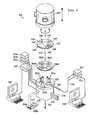
- FIG. 3there is a schematic diagram illustrating the basic components of a single vacuum chamber 300 that was used to prepare and encapsulate calcium-only patches 100 ′.
- the single-vacuum chamber 300is equipped with three evaporation boat electrodes 302 a , 302 b and 302 c each of which is associated with an individual shadow mask 304 a , 304 b and 304 c that will be used to evaporate a material (calcium 104 ′) in a unique pattern onto three of the four substrates 106 ′ placed on a platform 305 ′.
- the single-vacuum chamber 300also has a RF sputter gun 306 that will be used to deposit the candidate tin fluorophosphate glass 102 ′ through a mask 304 d and encapsulate each of the calcium covered substrates 106 ′ (only one encapsulated calcium-only patch 100 ′ has been shown on the platform 305 ′).
- the single-vacuum chamber 300was designed so it could be cryo-pumped (CTI-8200/Helix; Ma) to operate at pressures (10 ⁇ 6 -10 ⁇ 5 Torr) which are typical for evaporation processes but are also more than adequate for RF sputter deposition conditions ( ⁇ 10 ⁇ 3 Torr).
- Each evaporation boat electrode 302 a , 302 b and 302 cwas outfitted with two leads 308 a and 308 b (in this case copper leads 308 a and 308 b where only one pair of the leads 308 a and 308 b have been shown) so they could provide DC currents in the 80-180 Watt range through a vacuum 314 to a boat 310 which holds a calcium shot 312 .
- the effective resistance of a particular tungsten boat geometrydetermines the precise wattage which should be used to deposit/evaporate the calcium 312 (which forms the inner layer 104 ′) onto the substrate 106 ′.
- 3′′ ⁇ 3 ⁇ 4′′ tungsten boats 310were selected so stable deposition rates as high as 15 ⁇ /s could be attained.
- a water-cooled 3′′ diameter cylindrical RF sputtering gun 306(Onyx-3TM, Angstrom Sciences, Pa) was selected and positioned as shown in FIG. 3 .
- the RF sputtering gun 306has a water coupling 316 , an electrical coupling 318 (associated with a power supply 320 , feedback control 322 and computer 324 ) and an argon coupling 326 to be able to provide the desired RF deposition conditions: 30 Watt forward power ( ⁇ 1 Watt reflected power), 20 sccm argon flow leak rate, and a ⁇ 1 milliTorr chamber pressure with argon flow.
- pellets of calcium shot 312(Stock#10127 Alfa Aesar which was stored in a nitrogen purge box) were placed onto the 3′′ ⁇ 3 ⁇ 4′′ tungsten boats 310 . Each boat 310 was clamped firmly between the two copper leads 308 a and 308 b to complete the DC circuit required for Joule heating and evaporation.
- the three shadow masks 304 a , 304 b and 304 c containing L-shaped stencil patternswere positioned between the three evaporation boats 302 a , 302 b and 302 c and the three substrates 106 ′ (Corning 1737 glass substrate 106 ′).
- the single-vacuum chamber 300was then closed with a cover 328 and pumped until a vacuum was obtained in the 10 ⁇ 6 -10 ⁇ 5 Torr range. Initially, power in the 20-Watt range was delivered to each tungsten boat 310 for approximately 10 minutes then a “pre-soak” step was performed where the power was increased to ⁇ 80-125 Watts while depositing each 40 nm thick L-shaped calcium pattern 104 ′ onto three substrates 106 ′.
- a computer 330 attached to a thickness monitor 332 and three evaporation power supplies 334 a , 334 b and 334 c(respectively associated with the three evaporation boat electrodes 302 a , 302 b and 302 c ) controlled the deposition of the calcium patterns 104 ′ onto the three substrates 106 ′ (note: the platform 305 ′ shown has been rotated after the calcium 104 had been deposited onto the three substrates 106 ′ so the three calcium covered substrates 106 ′ are no longer located directly over the three masks 304 a , 304 b and 304 c ).
- the DC currentwas stopped and one of the patterned substrates 106 ′ was rotated into position above the mask 304 d and the RF sputtering gun 306 which contained the candidate tin fluorophosphate glass 102 ′ (see the shown position of the platform 305 ′).
- the RF sputtering gun 306deposited a ⁇ 2 micron thick film 102 ′ over the L-shaped calcium patterns 104 ′ on one of the substrates 106 ′ to form the encapsulated calcium-only patch 100 ′.
- this stepcould be repeated to encapsulate all of the L-shaped calcium patterns 104 ′ on all of the substrates 106 ′ (note: only one encapsulated calcium-only patch 100 ′, two substrates 106 ′ with calcium patterns 104 ′ and one plain substrate 106 ′ on the platform 305 ′ have been shown).
- 3′′ sealing targetswere prepared at a deposition rate that was estimated to be in a range near 1 ⁇ /second. The RF power, water, and argon were stopped, the cover 328 removed and the encapsulated L-shaped calcium patches 100 ′ was then removed for 85° C./85% RH testing. No post-deposition heat treatment was applied during the encapsulation process.
- FIG. 4there is a block diagram of an 85° C./85% accelerated-aging chamber/oven 400 which was used to test the hermeticity of one sealed calcium-only patch 100 ′ that was made in accordance with the non-heat treatment sealing method 200 of the present invention.
- the encapsulated calcium-only patch 100 ′ shownwas made during an experiment where only one substrate 106 ′ was placed within the single vacuum chamber 300 .
- the resulting encapsulated calcium-only patch 100 ′was then placed in the oven 400 and subjected to environmental aging at a fixed temperature 85° C. and 85% relative humidity (“85/85 testing”).
- the Ca layer 104 ′is initially a highly reflecting metallic mirror.
- the metallic Ca 104 ′would react and turn into an opaque white flaky crust which can be quantified with an optical measurement to estimate the amount of time the encapsulated device 100 ′ could theoretically operate in ambient conditions. For instance, it is believed that if the encapsulated calcium-only patch 100 ′ can survive 1000 hours in the oven 400 then that particular sealing material 102 could be used to seal an OLED display 100 which would then be able to operate for at least five years in normal ambient conditions.
- the hermetically sealed device 100would have an oxygen permeance of less than 0.01 cc/m 2 /atm/day and a water permeance of less than 0.01 g/m 2 /day.
- FIG. 5there is a time sequence of photos showing one of the L-shaped encapsulated calcium layers 104 ′ on the non-heat treated sealed calcium-only patch 100 ′ at different times within the 85° C./85% accelerated-aging chamber/oven 400 .
- the tested sealed calcium-only patch 100 ′ and in particular the non-heat treated candidate tin fluorophosphate glass 102 ′was able to inhibit oxygen and moisture penetration while in the 85° C./85% accelerated-aging chamber/oven 400 .
- the numbersindicate the hours the non-heat treated sealed calcium-only patch 100 ′ had endured the 85° C./85% environment.
- the same system 300was also later modified and used to make and successfully hermetically seal a homemade OLED.
- An important aspect of the non-heat treat sealing method 200is that a post deposition heat treatment step is not required to manufacture the hermetically sealed device 100 . This is desirable since in the past a heat treatment step was performed to remove/minimize defects (e.g., pores) within the deposited sealing material 102 where the defects had formed during the deposition step. But, it was a concern by performing this heat treating that the sealed device 100 and in particular the inner layer(s)/component(s) 104 could be damaged by the heat. Hence, in the co-pending U.S. patent application Ser. Nos. 11/207,691, 11/803,512 and 11/820,855 there was an attempt to reduce the temperature of this heat treatment step to avoid thermally damaging the specific device 100 .
- the present inventionrelates to a non-heat treat sealing method 200 used to manufacture a hermetically sealed device 100 .
- the non-heat treat sealing method 200includes the steps of: (1) positioning the un-encapsulated device 104 and 106 in a desired location with respect to a deposition device 300 ; and (2) using the deposition device 300 to deposit a sealing material 102 over at least a portion of the un-encapsulated device 104 and 106 to form a hermetically sealed device 100 without having to perform a post-deposition heat treating step.
- the preferred sealing material 102is a LLT material 102 or a Sn 2+ -containing inorganic oxide material 102 .
- the preferred sealing material(s) 102are specifically suited for inhibiting oxygen or/and moisture degradation which is a common problem to a wide variety of devices 100 including electronic devices, food containers and medicine containers.
- the preferred sealing material(s) 102may be used to reduce, for example, photochemical, hydrolytic, and oxidative damage to a device 100 due to chemically active permeants.
- the sealing materials 102may be used to prepare hermetic thin film ( ⁇ 2 ⁇ m) barrier layers that fulfill the most stringent impermeability requirements for OLED long-lived operation ( ⁇ 10 ⁇ 6 water gm/m 2 per day), and may be rapidly sputter-deposited on devices (or substrate materials) at extremely low temperatures ( ⁇ 40° C.).
- the devices 100include but are not limited to:
- the substrate materialsinclude but are not limited to:
- Sputter deposition, evaporation, and other thin film deposition processesmay be used to deposit the sealing material 102 .
- high rate deposition of Sn 2+ -containing inorganic oxide films 102may be produced by evaporation of metallic tin in an oxygen containing environment onto a rolling substrate such as plastic at very high speed.
- reactive DC sputtering of metallic tin in an oxygen environmentmay be used to produce the desired high rate deposition of a Sn 2+ -containing inorganic oxide film onto a device 100 .
- the sealing material 102can be batched with different powders/dopants to create a composition designed to achieve a specific physical-chemical property in the deposited barrier layer. Following is an exemplary list of various dopants that can be mixed with the sealing material 102 to achieve a desired physico-chemical property within the deposited barrier layer:
- Pattern-AbilitySputter deposition, or other thin film deposition methods, allow different patterning techniques to be used, such as shadow masking etc., to produce micro-structures having specific dielectric properties to help optimize the operation of the device 100 (e.g., an organic thin film transistor (TFT) device 100 could have insulator gates formed thereon to help achieve a good voltage threshold value).
- TFTorganic thin film transistor
Landscapes
- Chemical & Material Sciences (AREA)
- Materials Engineering (AREA)
- Engineering & Computer Science (AREA)
- Chemical Kinetics & Catalysis (AREA)
- Organic Chemistry (AREA)
- General Chemical & Material Sciences (AREA)
- Geochemistry & Mineralogy (AREA)
- Life Sciences & Earth Sciences (AREA)
- Mechanical Engineering (AREA)
- Metallurgy (AREA)
- Physics & Mathematics (AREA)
- Optics & Photonics (AREA)
- Electroluminescent Light Sources (AREA)
- Joining Of Glass To Other Materials (AREA)
- Glass Compositions (AREA)
Abstract
Description
This patent application is a continuation-in-part application of co-assigned U.S. patent application Ser. Nos. 11/820,855, filed, Jun. 21, 2007 now U.S. Pat. No. 7,722,929, which is a continuation-in-part of 11/207,691, filed Aug. 18, 2005, and U.S. patent application Ser. No. 11/803,512, filed May 15, 2007 now abandoned. The contents of these documents are hereby incorporated by reference herein.
The present invention relates to a method for hermetically sealing a device without needing to perform a heat treating step and the resulting hermetically sealed device. Examples of the hermetically sealed device include a light-emitting device (e.g., organic emitting light diode (OLED) device), a photovoltaic device, a thin-film sensor, an evanescent waveguide sensor, a food container and a medicine container.
Transport of oxygen and/or water through laminated or encapsulated materials and their subsequent attack on an inner material within a device represents two of the more common degradation mechanisms associated with many devices including, for example, light-emitting devices (OLED devices), thin-film sensors, evanescent waveguide sensors, food containers and medicine containers. For a detailed discussion about the problems associated with the penetration of oxygen and water into the inner layers (cathode and electro-luminescent materials) of an OLED device, reference is made to the following documents:
- Aziz, H., Popovic, Z. D., Hu, N. X., Hor, A. H., and Xu, G. “Degradation Mechanism of Small Molecule-Based Organic Light-Emitting Devices”, Science, 283, pp. 1900-1902, (1999).
- Burrows, P. E., Bulovic., V., Forrest, S. R., Sapochak, L. S., McCarty, D. M., Thompson, M. E. “Reliability and Degradation of Organic Light Emitting Devices”, Applied Physics Letters, 65(23), pp. 2922-2924.
- Kolosov, D., et al., Direct observation of structural changes in organic light emitting devices during degradation. Journal of Applied Physics, 1001. 90(7).
- Liew, F. Y., et al., Investigation of the sites of dark spots in organic light-emitting devices. Applied Physics Letters, 1000. 77(17).
- Chatham, H., “Review: Oxygen Diffusion Barrier Properties of Transparent Oxide Coatings on Polymeric Substrates”, 78, pp. 1-9, (1996).
It is well known that unless something is done to minimize the penetration of oxygen and water into an OLED device, then their operating lifetime will be severely limited. As a result, much effort has been expended to minimize the penetration of oxygen and water into an OLED device so as to help drive the OLED operation towards a 40 kilo-hour lifetime, the level generally regarded as necessary so OLED devices can overtake older device technologies such as LCD displays as discussed in the following document:
- Forsythe, Eric, W., “Operation of Organic-Based Light-Emitting Devices, in Society for Information Device (SID) 40thanniversary Seminar Lecture Notes, Vol. 1, Seminar M5, Hynes Convention Center, Boston, Mass., May 20 and 24, (1002).
The more prominent efforts to date that have been performed to help extend the lifetime of OLED devices include gettering, encapsulating and using various sealing techniques. In fact, one common way for sealing an OLED device today is to apply and heat-treat (or UV treat) different types of epoxies, inorganic materials and/or organic materials to form a seal on the OLED device. For example, Vitex Systems manufactures and sells a coating under the brand name of Barix™ which is a composite based approach where alternate layers of inorganic materials and organic materials are used to seal the OLED device. Although these types of seals provide some level of hermetic behavior, they can be very expensive and there are still many instances in which they have failed over time to prevent the diffusion of oxygen and water into the OLED device.
To address this sealing problem, the assignee of the present invention has developed several different sealing techniques and sealing materials that can be used to hermetically seal an OLED device (or other type of device)(see the aforementioned U.S. patent application Ser. Nos. 11/207,691, 11/803,512 and 11/820,855). Although these sealing techniques and sealing materials work well to hermetically seal an OLED device (or other types of devices) there was still a desire to improve upon these sealing techniques and sealing materials so that one can more effectively hermetically seal an OLED device (or other type of device). This particular need and other needs have been satisfied by the present invention.
In one aspect, the present invention includes a method for hermetically sealing a device comprising the steps of: (1) positioning an un-encapsulated device in a desired location with respect to a deposition device; and (2) using the deposition device to deposit a sealing material over at least a portion of the un-encapsulated device to form a hermetically sealed device without having to perform a post-deposition heat treating step. In one embodiment, the sealing material is a Sn2+-containing inorganic oxide material or a low liquidus temperature inorganic material.
In another aspect, the present invention includes a device comprising a substrate plate, at least one component, and a non-heat treated sealing material, where the at least one component is hermetically sealed between the non-heat treated sealing material and the substrate plate. In one embodiment, the sealing material is a Sn2+-containing inorganic oxide material or a low liquidus temperature inorganic material.
In yet another aspect, the present invention includes an organic emitting light diode (OLED) device comprising a substrate plate, at least one organic light emitting diode, and a non-heat treated sealing material, where the at least one organic light emitting diode is hermetically sealed between the non-heat treated sealing material and the substrate plate. In one embodiment, the sealing material is a Sn2+-containing inorganic oxide material or a low liquidus temperature inorganic material.
Additional aspects of the invention will be set forth, in part, in the detailed description, figures and any claims which follow, and in part will be derived from the detailed description, or can be learned by practice of the invention. It is to be understood that both the foregoing general description and the following detailed description are exemplary and explanatory only and are not restrictive of the invention as disclosed.
A more complete understanding of the present invention may be had by reference to the following detailed description when taken in conjunction with the accompanying drawings wherein:
Referring toFIGS. 1-2 , there are respectively illustrated a cross-sectional side view of a hermetically sealeddevice 100 and a flowchart of a non-heattreatment sealing method 200 used to manufacture the hermetically sealeddevice 100 in accordance with the present invention. As shown inFIG. 1 , the non-heat treated hermetically sealeddevice 100 includes a sealing material102 (e.g., a Sn2+-containinginorganic oxide material 102 or a low liquidus temperature (LLT) inorganic material102) which was deposited so as to encapsulate and hermetically seal one or more inner layers/components 104 located on a support/substrate 106.
The non-heattreatment sealing method 200 includes apositioning step 202 in which anun-encapsulated device deposition device 300 discussed below with respect to FIG.3). Optionally, the deposition device may be located in a clean environment (or a cleanroom) where a clean process is practiced to prevent as much as possible the presence of large particulates from contaminating theun-encapsulated device sealing material 102. For instance, the clean environment or cleanroom could be designed to ensure that there are no particulates (or very few particulates) in the atmosphere which have a dimension greater than the final thickness of the sealingmaterial 102 on thedevice 100. A detailed discussion about the different types of cleanrooms that could be used is provided in the industry standards: (1) US Federal Standard 209 entitled “Cleanroom and Work Station Requirements, Controlled Environments” 1992; and (2) the International Standards Organization TC209. The contents of these two standards are hereby incorporated by reference herein.
The non-heattreatment sealing method 200 has anoptional cooling step 204 in which the support/substrate 106 and possibly the inner layer(s)/component(s)104 of theun-encapsulated device optional cooling step 204 is that by cooling theun-encapsulated device material 102 could be deposited onto theun-encapsulated device device 100. This is important when one wants to have a high volume operation and manufacture a large number of hermetically sealeddevices 100. For a more detailed discussion about thisoptional cooling step 204, reference is made to the aforementioned U.S. patent application Ser. No. 11/820,855 filed on Jun. 21, 2007 and entitled “Sealing Technique for Decreasing the Time it Takes to Hermetically Seal a Device and the Resulting Hermetically Sealed Device”.
In addition, the non-heattreatment sealing method 200 has adeposition step 206 in which the deposition device is used to deposit the sealing material102 (e.g., Sn2+-containinginorganic oxide material 102 or LLT material102) over the inner layer(s)/component(s)104 located on top of the support/substrate 106 to form the hermetically sealeddevice 100. In one embodiment, thesealing material 102 can be deposited over the inner layer(s)/component(s)104 and the support/substrate 106 at a deposition rate which is (for example): preferably ˜5 Å/second, more preferably ˜25 Å/second, and even more preferably ˜75 Å/second. Plus, the sealingmaterial 102 can be deposited by using any one of variety of processes including, for example, sputtering, flash evaporation, spraying, pouring, frit-deposition, vapor-deposition, dip-coating, painting, rolling (for example using a film of sealing material102), spin-coating, a co-evaporation process, a soot gun spraying process, a reactive sputtering process, a magnetron radio-frequency (RF) sputtering process, a laser ablation process, or any combination thereof.
If desired, thedeposition step 206 can be performed in an inert atmosphere or in a vacuum to help ensure that a water and an oxygen-free condition is maintained throughout theentire sealing process 200. This type of processing environment would help to ensure the robust, long-life operation of organic electronics104 (for example) that may be located within the hermetically sealeddevice 100. An important aspect of the non-heattreatment sealing method 200 is that a post deposition heat treatment step is not required to make the hermetically sealeddevice 100. The advantages associated with using the non-heattreatment sealing method 200 are discussed below with respect to a hermetically sealedOLED device 100.
Examples ofdifferent devices 100 that can be protected by the non-heat treated sealing material102 (e.g., Sn2+-containinginorganic oxide material 102 and LLT material102) include a light-emitting device (e.g., OLED device), a photovoltaic device, a thin-film sensor, an evanescent waveguide sensor, a food container, and a medicine container. If thedevice 102 is anOLED device 100, then theinner layers 104 include cathode and electro-luminescent materials which form organic light emitting diode(s)104 that are located on thesubstrate 106. The organic light emitting diode(s)104 can be damaged if they are heated above for example 100-125° C. As such, it is very desirable that thesealing method 200 does not require the use of a heat treatment step.
To help implement the non-heattreatment sealing method 200, the sealingmaterial 102 used to encapsulate and hermetically seal thedevice 100 would preferably be a LLTinorganic material 102 or a Sn2+-containinginorganic oxide material 102. These sealingmaterials 102 are discussed below but for a more detailed discussion about these sealing materials reference is made to the co-assigned and co-pending U.S. patent application Ser. Nos. 11/207,691 and 11/803,512.
TheLLT material 102 is useful in the non-heattreatment sealing method 200 because this type of material can be applied such that there is a pore-free film formed on thedevice 100. In one embodiment, theLLT material 102 has a low liquidus temperature ≦1000° C. (and more preferably ≦600° C. and even more preferably ≦400° C.). TheLLT material 102 can include, for example, glass such as tin fluorophosphate glass, tungsten-doped tin fluorophosphate glass, chalcogenide glass, tellurite glass, borate glass and phosphate glass (e.g., alkali Zn or SnZn pyrophosphates). An exemplary tin fluorophosphate glass has the following composition: Sn (20-85 wt %), P (2-20 wt %), O (10-36 wt %), F (10-36 wt %), Nb (0-5 wt %) and at least 75% total of Sn+P+O+F (which can be melted powder targets or sputtered pressed powder targets). TheseLLT materials 102 are desirable for several different reasons including (for example):
- The
LLT material 102 can be devoid of heavy metals and other environmentally undesirable materials. - The
LLT material 102 can be durable and exhibit low dissolution rates when immersed in water at 85° C. - The
LLT material 102 can contain dye molecules and can be doped to levels as high as 8 mM (4.8×1018cm−3). - The LLT phosphate glasses have helium permeability coefficients 4 to 5 orders of magnitude less than that of fused silica.
- The
Alternatively, anotherLLT material 102 namely tungsten-doped tin fluorophosphate glass could be used in this non-heattreatment sealing method 200 and this material was disclosed in co-assigned U.S. patent application Ser. No. 11/544,262 (the contents of which are incorporated by reference herein). An exemplary tungsten-doped tin fluorophosphate glass has the following composition: (55-75 wt %) Sn, (4-14 wt %) P, (6-24 wt %) O, (4-22 wt %) F, and (0.15-15 wt %) W.
The Sn2+-containinginorganic oxide material 102 is useful in the non-heattreatment sealing method 200 because this type of material has the ability to form a hermetic encapsulated coating which protects thedevice 100. In one embodiment, the Sn2+-containinginorganic oxide material 102 has a composition with molar limits 36-100% SnO, 0-45% SnF2, and 0-28% P2O5which roughly correspond to the following elemental weight percentages: 59-89 wt % Sn, 0-13 wt % P, 6-25 wt % O, and 0-12 wt % F. In another embodiment, the Sn2+-containinginorganic oxide materials 102 include: (1) SnO; (2) SnO and a borate material; (3) SnO and a phosphate material; and (4) SnO and a borophosphate material. For instance, the Sn2+-containinginorganic oxide materials 102 can include compositions such as, for example, SnO powder, blended SnO/P2O5-containing powders (e.g., 80% SnO+20% P2O5), and blended SnO/BPO4powders (e.g., 90% SnO+10% BPO4). Alternatively, the Sn2+-containinginorganic oxide material 102 can include blended compositions that had been melted to form the appropriate sputtering target (e.g., 80% SnO+20% P2O5). Typically, the Sn2+-containinginorganic oxide material 102 contains >50% stannous oxide (and more preferably >70% stannous oxide and even more preferably >80% stannous oxide).
The results associated with testing a candidate tin fluorophosphate glass102 (LLT material102) which had the following composition: Sn (22.42 wt %), P (11.48 wt %), O (42.41 wt %), F (22.64 wt %) and Nb (1.05 wt %) that was deposited onto anun-encapsulated device FIGS. 3-5 . In this experiment, the candidatetin fluorophosphate glass 102 underwent a “calcium-only patch” test which was performed to determine how well it inhibited the penetration of oxygen and moisture. Prior to discussing the results of the experiment, a discussion is provided to explain how a calcium-only patch test is set-up and then performed to check the feasibility of the non-heattreatment sealing method 200.
Referring toFIG. 3 , there is a schematic diagram illustrating the basic components of asingle vacuum chamber 300 that was used to prepare and encapsulate calcium-onlypatches 100′. As shown, the single-vacuum chamber 300 is equipped with threeevaporation boat electrodes individual shadow mask calcium 104′) in a unique pattern onto three of the foursubstrates 106′ placed on aplatform 305′. The single-vacuum chamber 300 also has aRF sputter gun 306 that will be used to deposit the candidatetin fluorophosphate glass 102′ through amask 304dand encapsulate each of the calcium coveredsubstrates 106′ (only one encapsulated calcium-onlypatch 100′ has been shown on theplatform 305′).
The single-vacuum chamber 300 was designed so it could be cryo-pumped (CTI-8200/Helix; Ma) to operate at pressures (10−6-10−5Torr) which are typical for evaporation processes but are also more than adequate for RF sputter deposition conditions (˜10−3Torr). Eachevaporation boat electrode leads leads vacuum 314 to aboat 310 which holds acalcium shot 312. Typically, the effective resistance of a particular tungsten boat geometry determines the precise wattage which should be used to deposit/evaporate the calcium312 (which forms theinner layer 104′) onto thesubstrate 106′. In this case, 3″×¾″tungsten boats 310 were selected so stable deposition rates as high as 15 Å/s could be attained. And, a water-cooled 3″ diameter cylindrical RF sputtering gun306 (Onyx-3™, Angstrom Sciences, Pa) was selected and positioned as shown inFIG. 3 . TheRF sputtering gun 306 has awater coupling 316, an electrical coupling318 (associated with apower supply 320,feedback control 322 and computer324) and anargon coupling 326 to be able to provide the desired RF deposition conditions: 30 Watt forward power (˜1 Watt reflected power), 20 sccm argon flow leak rate, and a ˜1 milliTorr chamber pressure with argon flow.
Prior to depositing thecalcium 104 onto the threesubstrates 106′, pellets of calcium shot312 (Stock#10127 Alfa Aesar which was stored in a nitrogen purge box) were placed onto the 3″×¾″tungsten boats 310. Eachboat 310 was clamped firmly between the two copper leads308aand308bto complete the DC circuit required for Joule heating and evaporation. The threeshadow masks evaporation boats substrates 106′ (Corning 1737glass substrate 106′). The single-vacuum chamber 300 was then closed with acover 328 and pumped until a vacuum was obtained in the 10−6-10−5Torr range. Initially, power in the 20-Watt range was delivered to eachtungsten boat 310 for approximately 10 minutes then a “pre-soak” step was performed where the power was increased to ˜80-125 Watts while depositing each 40 nm thick L-shapedcalcium pattern 104′ onto threesubstrates 106′. Acomputer 330 attached to athickness monitor 332 and threeevaporation power supplies evaporation boat electrodes calcium patterns 104′ onto the threesubstrates 106′ (note: theplatform 305′ shown has been rotated after thecalcium 104 had been deposited onto the threesubstrates 106′ so the three calcium coveredsubstrates 106′ are no longer located directly over the threemasks
After the deposition of thecalcium patterns 104′, the DC current was stopped and one of the patternedsubstrates 106′ was rotated into position above themask 304dand theRF sputtering gun 306 which contained the candidatetin fluorophosphate glass 102′ (see the shown position of theplatform 305′). TheRF sputtering gun 306 deposited a ˜2 micronthick film 102′ over the L-shapedcalcium patterns 104′ on one of thesubstrates 106′ to form the encapsulated calcium-onlypatch 100′. Of course, this step could be repeated to encapsulate all of the L-shapedcalcium patterns 104′ on all of thesubstrates 106′ (note: only one encapsulated calcium-onlypatch 100′, twosubstrates 106′ withcalcium patterns 104′ and oneplain substrate 106′ on theplatform 305′ have been shown). In this experiment, 3″ sealing targets were prepared at a deposition rate that was estimated to be in a range near 1 Å/second. The RF power, water, and argon were stopped, thecover 328 removed and the encapsulated L-shapedcalcium patches 100′ was then removed for 85° C./85% RH testing. No post-deposition heat treatment was applied during the encapsulation process.
Referring toFIG. 4 , there is a block diagram of an 85° C./85% accelerated-aging chamber/oven 400 which was used to test the hermeticity of one sealed calcium-onlypatch 100′ that was made in accordance with the non-heattreatment sealing method 200 of the present invention. The encapsulated calcium-onlypatch 100′ shown was made during an experiment where only onesubstrate 106′ was placed within thesingle vacuum chamber 300. The resulting encapsulated calcium-onlypatch 100′ was then placed in theoven 400 and subjected to environmental aging at a fixed temperature 85° C. and 85% relative humidity (“85/85 testing”). In the encapsulated calcium-onlypatch 100′, theCa layer 104′ is initially a highly reflecting metallic mirror. And, if water and oxygen penetrate the candidatetin fluorophosphate glass 102′, then themetallic Ca 104′ would react and turn into an opaque white flaky crust which can be quantified with an optical measurement to estimate the amount of time the encapsulateddevice 100′ could theoretically operate in ambient conditions. For instance, it is believed that if the encapsulated calcium-onlypatch 100′ can survive 1000 hours in theoven 400 then thatparticular sealing material 102 could be used to seal anOLED display 100 which would then be able to operate for at least five years in normal ambient conditions. In this case, the hermetically sealeddevice 100 would have an oxygen permeance of less than 0.01 cc/m2/atm/day and a water permeance of less than 0.01 g/m2/day. For details about an earlier version of this calcium patch test which involved the use of an encapsulated calcium layer and aluminum layer to characterize the relative rate of water vapor and oxygen transport through prospective barriers on devices, reference is made to the co-pending U.S. patent application Ser. No. 11/803,512.
Referring toFIG. 5 , there is a time sequence of photos showing one of the L-shaped encapsulated calcium layers104′ on the non-heat treated sealed calcium-onlypatch 100′ at different times within the 85° C./85% accelerated-aging chamber/oven 400. As can be seen, the tested sealed calcium-onlypatch 100′ and in particular the non-heat treated candidatetin fluorophosphate glass 102′ was able to inhibit oxygen and moisture penetration while in the 85° C./85% accelerated-aging chamber/oven 400. The numbers indicate the hours the non-heat treated sealed calcium-onlypatch 100′ had endured the 85° C./85% environment. Thesame system 300 was also later modified and used to make and successfully hermetically seal a homemade OLED.
An important aspect of the non-heattreat sealing method 200 is that a post deposition heat treatment step is not required to manufacture the hermetically sealeddevice 100. This is desirable since in the past a heat treatment step was performed to remove/minimize defects (e.g., pores) within the deposited sealingmaterial 102 where the defects had formed during the deposition step. But, it was a concern by performing this heat treating that the sealeddevice 100 and in particular the inner layer(s)/component(s)104 could be damaged by the heat. Hence, in the co-pending U.S. patent application Ser. Nos. 11/207,691, 11/803,512 and 11/820,855 there was an attempt to reduce the temperature of this heat treatment step to avoid thermally damaging thespecific device 100. In fact, in U.S. patent application Ser. No. 11/803,512 it was specifically stated that if SnO was the sealingmaterial 102 then there was no need to perform the heat treatment step. As discussed above, a subsequent experiment was conducted which indicated that a heat treatment step does not need to be performed when using the previously described sealingmaterials 102.
From the foregoing, it can be readily appreciated by those skilled in the art that the present invention relates to a non-heattreat sealing method 200 used to manufacture a hermetically sealeddevice 100. The non-heattreat sealing method 200 includes the steps of: (1) positioning theun-encapsulated device deposition device 300; and (2) using thedeposition device 300 to deposit a sealingmaterial 102 over at least a portion of theun-encapsulated device device 100 without having to perform a post-deposition heat treating step. Thepreferred sealing material 102 is aLLT material 102 or a Sn2+-containinginorganic oxide material 102. If desired multiple layers of the same or different types of the sealingmaterials 102 can be deposited on top of thedevice 100. As discussed above, the preferred sealing material(s)102 are specifically suited for inhibiting oxygen or/and moisture degradation which is a common problem to a wide variety ofdevices 100 including electronic devices, food containers and medicine containers. In addition, the preferred sealing material(s)102 may be used to reduce, for example, photochemical, hydrolytic, and oxidative damage to adevice 100 due to chemically active permeants. Some additional advantages and features of using these particular sealing material(s)102 are as follows:
The sealingmaterials 102 may be used to prepare hermetic thin film (˜2 μm) barrier layers that fulfill the most stringent impermeability requirements for OLED long-lived operation (<10−6water gm/m2per day), and may be rapidly sputter-deposited on devices (or substrate materials) at extremely low temperatures (<40° C.). Thedevices 100 include but are not limited to:
- a. Organic electronic devices
- Organic light-emitting diodes (OLED)s
- Organic photovoltaic devices (OPV)s
- Organic Sensors, with or without catalysts
- Flexible substrates for flexible flat panel devices
- Radio frequency identification tags (RFID)s
- b. Semiconductor electronic devices
- Light-emitting diodes (LED)s
- Photovoltaic devices (PV)s
- Sensors, with or without catalysts
- Flexible substrates for flexible flat panel devices
- Radio frequency identification tags (RFID)s
- a. Organic electronic devices
The substrate materials include but are not limited to:
- a. Polymer Materials
- Flexible substrates for flexible flat panel devices
- Food packaging
- Medical packaging
- a. Polymer Materials
B. The deposition of organicelectronic devices 100 with theseparticular sealing materials 102 requires no introduction of oxygen or air into the clean environment/cleanroom. The fact that no outside oxidizing source is required to enable the sealing event makes this sealing technique an attractive feature for making organic electronic devices. This is especially true since it is well known that oxygen and moisture are the principal degrading reactants associated with the redox and photo-bleaching degradation reactions which adversely affect the organic layers and/or cathode materials that are located within organic electronic devices like an OLED.
C. Sputter deposition, evaporation, and other thin film deposition processes may be used to deposit the sealingmaterial 102. For example, high rate deposition of Sn2+-containinginorganic oxide films 102 may be produced by evaporation of metallic tin in an oxygen containing environment onto a rolling substrate such as plastic at very high speed. Alternatively, reactive DC sputtering of metallic tin in an oxygen environment may be used to produce the desired high rate deposition of a Sn2+-containing inorganic oxide film onto adevice 100. In fact, there are many different thin film deposition techniques that could be used to deposit the Sn2+-containing inorganic oxide film102 (and the LLT film102) onto thedevice 100.
D. The sealingmaterial 102 can be batched with different powders/dopants to create a composition designed to achieve a specific physical-chemical property in the deposited barrier layer. Following is an exemplary list of various dopants that can be mixed with the sealingmaterial 102 to achieve a desired physico-chemical property within the deposited barrier layer:
- a. Opacity-Transparency: For instance, SnO is opaque at visible wavelengths, but it may be doped with components such as phosphates to yield transparent films.
- b. Refractive Index: Dopants such as P2O5, BPO4and PbF2can be used to alter the refractive index of the sealing
material 102 to help optimize, for instance, the light transmission and/or light extraction of thedevice 100. For example,OLED devices 100 with top emission can be optimized when the air gaps therein are replaced with an index-matched oxide material. - c. Coefficient of Thermal Expansion (CTE): Dopants such as SnF2, P2O5and PbF2can be used to alter the CTE of the sealing
material 102 which can help to minimize the different forms of delamination which are commonly associated with “CTE mismatch” problems. - d. Sensitization: Phosphors, quantum dots, inorganic/organic dyes and molecules may be added to confer desired electro-optic characteristics which are useful for device optimization. For instance, dopants such as carbon black can be used to alter the electro-optic character (Fermi level/resistivity) of the sealing
material 102 to improve the efficiency of the hermetically sealed device100 (note: if the Fermi level can be shifted substantially then this might enable one to alter the conductivity of the barrier film in a manner which is analogous to the known indium-tin-oxide (ITO) systems). - e. Alter Solubility and Interface Wettability for Better Adhesion: Doping the sealing
material 102 with dopants, such as SnF2, enables one to alter the miscibility of the deposited barrier film. If desired, this concept may be further exploited for adhesion purposes by altering the surface wet-ability of the sealingmaterial 102. - f. Scratch Resistant: Dopants such as SnO, SnF2and PbF2may be used to confer a hardness in the sealing
material 102 which may be desirable forvarious devices 100.
E. Pattern-Ability: Sputter deposition, or other thin film deposition methods, allow different patterning techniques to be used, such as shadow masking etc., to produce micro-structures having specific dielectric properties to help optimize the operation of the device100 (e.g., an organic thin film transistor (TFT)device 100 could have insulator gates formed thereon to help achieve a good voltage threshold value).
Although several embodiments of the present invention have been illustrated in the accompanying Drawings and described in the foregoing Detailed Description, it should be understood that the invention is not limited to the embodiments disclosed, but is capable of numerous rearrangements, modifications and substitutions without departing from the spirit of the invention as set forth and defined by the following claims.
Claims (10)
1. A method for hermetically sealing a device, said method comprising the steps of:
positioning an un-encapsulated device in a desired location with respect to a deposition device; and
using the deposition device to deposit an Sn2+-containing inorganic oxide sealing material over at least a portion of the un-encapsulated device to form a hermetically sealed device without performing a post-deposition heat treating step; and
wherein the Sn2+-containing inorganic oxide sealing material has the following composition,
Sn (59-89 wt %);
P (0-13 wt %);
O (6-25 wt %); and
F (0-12 wt %).
2. The method ofclaim 1 , further comprising the step of cooling said device prior to depositing the Sn2+-containing inorganic oxide sealing material over said device.
3. The method ofclaim 1 , wherein said deposition device is located within a clean room.
4. The method ofclaim 1 , wherein said deposited Sn2+-containing inorganic oxide sealing material has a thickness in a range of about 2 μm.
5. The method ofclaim 1 , wherein said using step includes utilizing a RF sputtering process to deposit the Sn2+-containing inorganic oxide scaling material over said device at a deposition rate in a range of about 5 Å/second to about 75 Å/second.
6. The method ofclaim 1 , wherein said hermetically scaled device has an oxygen permeance of less than 0.01 cc/m2/atm/day and a water permeance of less than 0.01 g/m2/day.
7. The method ofclaim 1 , wherein said sealing material is doped with a dopant to achieve a desired specific physical-chemical property including one of the following, or any combination thereof:
an opacity-transparency;
a refractive index;
a coefficient of thermal expansion;
a sensitization;
a fermi level/resistivity;
a solubility/interface wettability; and
a hardness.
8. The method ofclaim 1 , wherein said hermetically sealed device is a selected one of:
an organic-electronic device including:
an organic emitting light diode (OLED),
a polymer light emitting diode (PLED),
a photovoltaic,
a metamaterial,
a thin film transistor; and
a waveguide;
an inorganic-electronic device including:
a light emitting diode (LED),
a photovoltaic,
a metamaterial,
a thin film transistor; and
a waveguide;
an optoelectronic device including:
an optical switch;
a waveguide;
a flexible substrate;
a food container; and
a medical container.
9. The method ofclaim 1 , wherein the Sn2+-containing inorganic oxide sealing material comprises greater than 80% stannous oxide.
10. The method ofclaim 1 , wherein the Sn2+-containing inorganic oxide sealing material is deposited as a single, pore-free layer.
Priority Applications (6)
| Application Number | Priority Date | Filing Date | Title |
|---|---|---|---|
| US12/072,784US7829147B2 (en) | 2005-08-18 | 2008-02-28 | Hermetically sealing a device without a heat treating step and the resulting hermetically sealed device |
| PCT/US2009/001190WO2009108313A1 (en) | 2008-02-28 | 2009-02-26 | Hermetically sealing a device without a heat treating step and the resulting hermetically sealed device |
| EP09714201AEP2258008A1 (en) | 2008-02-28 | 2009-02-26 | Hermetically sealing a device without a heat treating step and the resulting hermetically sealed device |
| JP2010548710AJP2011513916A (en) | 2008-02-28 | 2009-02-26 | Hermetic sealing of the device and this hermetically sealed device without a heat treatment step |
| TW098106274ATWI409347B (en) | 2008-02-28 | 2009-02-26 | Hermetically sealing a device without a heat treating step and the resulting hermetically sealed device |
| US12/894,474US8304990B2 (en) | 2005-08-18 | 2010-09-30 | Hermetically sealing a device without a heat treating step and the resulting hermetically sealed device |
Applications Claiming Priority (4)
| Application Number | Priority Date | Filing Date | Title |
|---|---|---|---|
| US11/207,691US20070040501A1 (en) | 2005-08-18 | 2005-08-18 | Method for inhibiting oxygen and moisture degradation of a device and the resulting device |
| US11/803,512US20080206589A1 (en) | 2007-02-28 | 2007-05-15 | Low tempertature sintering using Sn2+ containing inorganic materials to hermetically seal a device |
| US11/820,855US7722929B2 (en) | 2005-08-18 | 2007-06-21 | Sealing technique for decreasing the time it takes to hermetically seal a device and the resulting hermetically sealed device |
| US12/072,784US7829147B2 (en) | 2005-08-18 | 2008-02-28 | Hermetically sealing a device without a heat treating step and the resulting hermetically sealed device |
Related Parent Applications (2)
| Application Number | Title | Priority Date | Filing Date |
|---|---|---|---|
| US11/207,691Continuation-In-PartUS20070040501A1 (en) | 2005-08-18 | 2005-08-18 | Method for inhibiting oxygen and moisture degradation of a device and the resulting device |
| US11/820,855Continuation-In-PartUS7722929B2 (en) | 2005-08-18 | 2007-06-21 | Sealing technique for decreasing the time it takes to hermetically seal a device and the resulting hermetically sealed device |
Related Child Applications (1)
| Application Number | Title | Priority Date | Filing Date |
|---|---|---|---|
| US12/894,474DivisionUS8304990B2 (en) | 2005-08-18 | 2010-09-30 | Hermetically sealing a device without a heat treating step and the resulting hermetically sealed device |
Publications (2)
| Publication Number | Publication Date |
|---|---|
| US20080149924A1 US20080149924A1 (en) | 2008-06-26 |
| US7829147B2true US7829147B2 (en) | 2010-11-09 |
Family
ID=40640245
Family Applications (2)
| Application Number | Title | Priority Date | Filing Date |
|---|---|---|---|
| US12/072,784Expired - Fee RelatedUS7829147B2 (en) | 2005-08-18 | 2008-02-28 | Hermetically sealing a device without a heat treating step and the resulting hermetically sealed device |
| US12/894,474Expired - Fee RelatedUS8304990B2 (en) | 2005-08-18 | 2010-09-30 | Hermetically sealing a device without a heat treating step and the resulting hermetically sealed device |
Family Applications After (1)
| Application Number | Title | Priority Date | Filing Date |
|---|---|---|---|
| US12/894,474Expired - Fee RelatedUS8304990B2 (en) | 2005-08-18 | 2010-09-30 | Hermetically sealing a device without a heat treating step and the resulting hermetically sealed device |
Country Status (5)
| Country | Link |
|---|---|
| US (2) | US7829147B2 (en) |
| EP (1) | EP2258008A1 (en) |
| JP (1) | JP2011513916A (en) |
| TW (1) | TWI409347B (en) |
| WO (1) | WO2009108313A1 (en) |
Cited By (30)
| Publication number | Priority date | Publication date | Assignee | Title |
|---|---|---|---|---|
| US20090121333A1 (en)* | 2006-11-30 | 2009-05-14 | Bruce Gardiner Aitken | Flexible substrates having a thin-film barrier |
| US20100193353A1 (en)* | 2005-08-18 | 2010-08-05 | Bruce Gardiner Aitken | Sealing technique for decreasing the time it takes to hermetically seal a device and the resulting hermetically sealed device |
| US8778713B2 (en) | 2012-08-28 | 2014-07-15 | Samsung Display Co., Ltd. | Encapsulation sheet, method of manufacturing organic light emitting display device using the same, and organic light emitting display device |
| WO2014116630A1 (en) | 2013-01-28 | 2014-07-31 | Corning Incorporated | Flexible hermetic thin film with light extraction layer |
| US9054336B2 (en) | 2012-03-02 | 2015-06-09 | Samsung Display Co., Ltd. | Organic light-emitting display device |
| US9096933B2 (en) | 2009-07-08 | 2015-08-04 | Aixtron, Inc. | Methods for plasma processing |
| US9276234B2 (en) | 2012-03-02 | 2016-03-01 | Samsung Display Co., Ltd. | Method of preparing organic light emitting device |
| US9299956B2 (en) | 2012-06-13 | 2016-03-29 | Aixtron, Inc. | Method for deposition of high-performance coatings and encapsulated electronic devices |
| US9306187B2 (en) | 2013-04-30 | 2016-04-05 | Samsung Display Co., Ltd. | Organic light-emitting display device and method of manufacturing the same |
| US9349989B2 (en) | 2013-02-07 | 2016-05-24 | Samsung Display Co., Ltd. | Organic luminescence emitting display device and method of manufacturing the same |
| US9359674B2 (en) | 2011-01-10 | 2016-06-07 | Aixtron, Inc. | Apparatus and method for dielectric deposition |
| US9515286B2 (en) | 2013-05-10 | 2016-12-06 | Corning Incorporated | Laser welding transparent glass sheets using low melting glass or thin absorbing films |
| US9515287B2 (en) | 2013-07-30 | 2016-12-06 | Samsung Display Co., Ltd. | Organic light-emitting display apparatus having encapsulation layer of low temperature viscosity transition and method of manufacturing the same |
| US9555595B2 (en) | 2010-04-20 | 2017-01-31 | Corning Incorporated | Multi-laminate hermetic barriers and related structures and methods of hermetic sealing |
| US9634286B2 (en) | 2012-08-31 | 2017-04-25 | Samsung Display Co., Ltd | Display panel and manufacturing method of the same |
| US9666763B2 (en) | 2012-11-30 | 2017-05-30 | Corning Incorporated | Glass sealing with transparent materials having transient absorption properties |
| US9685628B2 (en) | 2013-08-16 | 2017-06-20 | Samsung Electronics Co., Ltd. | Methods for making optical components, optical components, and products including same |
| US20170327419A1 (en)* | 2014-10-31 | 2017-11-16 | Corning Incorporated | Laser welded glass packages and methods of making |
| US10017849B2 (en) | 2012-11-29 | 2018-07-10 | Corning Incorporated | High rate deposition systems and processes for forming hermetic barrier layers |
| US10497898B2 (en) | 2015-11-24 | 2019-12-03 | Corning Incorporated | Sealed device housing with particle film-initiated low thickness laser weld and related methods |
| US10526708B2 (en) | 2012-06-19 | 2020-01-07 | Aixtron Se | Methods for forming thin protective and optical layers on substrates |
| US10627691B2 (en)* | 2009-03-31 | 2020-04-21 | View, Inc. | Temperable electrochromic devices |
| US10952621B2 (en) | 2017-12-05 | 2021-03-23 | Cardiac Pacemakers, Inc. | Multimodal analyte sensor optoelectronic interface |
| US11089983B2 (en) | 2017-12-01 | 2021-08-17 | Cardiac Pacemakers, Inc. | Multimodal analyte sensors for medical devices |
| US11129557B2 (en) | 2017-05-31 | 2021-09-28 | Cardiac Pacemakers, Inc. | Implantable medical device with chemical sensor |
| US11439304B2 (en) | 2017-08-10 | 2022-09-13 | Cardiac Pacemakers, Inc. | Systems and methods including electrolyte sensor fusion |
| US11560328B2 (en) | 2014-02-13 | 2023-01-24 | Corning Incorporated | Ultra low melting glass frit and fibers |
| US11571151B2 (en) | 2017-08-23 | 2023-02-07 | Cardiac Pacemakers, Inc. | Implantable chemical sensor with staged activation |
| US11877471B2 (en) | 2021-02-16 | 2024-01-16 | Samsung Display Co., Ltd. | Display apparatus and method of manufacturing the same |
| US12004853B2 (en) | 2017-07-26 | 2024-06-11 | Cardiac Pacemakers, Inc. | Systems and methods for disambiguation of posture |
Families Citing this family (22)
| Publication number | Priority date | Publication date | Assignee | Title |
|---|---|---|---|---|
| KR101709387B1 (en)* | 2012-02-27 | 2017-02-22 | 코닝 인코포레이티드 | Low Tg glass gasket for hermetic sealing applications |
| TW201343940A (en)* | 2012-03-14 | 2013-11-01 | Corning Inc | Sputtering targets and associated sputtering methods for forming hermetic barrier layers |
| DE102012109207B4 (en)* | 2012-09-28 | 2018-05-09 | Osram Oled Gmbh | Method and device for producing an optoelectronic component |
| US9202996B2 (en) | 2012-11-30 | 2015-12-01 | Corning Incorporated | LED lighting devices with quantum dot glass containment plates |
| KR101434367B1 (en)* | 2012-12-14 | 2014-08-27 | 삼성디스플레이 주식회사 | Organic light emitting display device and method of fabricating the same |
| KR20140101610A (en)* | 2013-02-12 | 2014-08-20 | 삼성디스플레이 주식회사 | Deposition apparatus and manufacturing method of organic light emitting display using the same |
| KR20140120541A (en)* | 2013-04-03 | 2014-10-14 | 삼성디스플레이 주식회사 | Organic light emitting device display and manufacturing method thereof |
| KR102072805B1 (en) | 2013-04-15 | 2020-02-04 | 삼성디스플레이 주식회사 | Organic luminescence emitting display device and method for preparing the same |
| KR102072806B1 (en)* | 2013-04-18 | 2020-03-03 | 삼성디스플레이 주식회사 | Organic light emitting display device and method of manufacturing the same |
| KR102080012B1 (en) | 2013-07-12 | 2020-02-24 | 삼성디스플레이 주식회사 | Organic light emitting display device and method of manufacturing the same |
| KR102093392B1 (en) | 2013-07-25 | 2020-03-26 | 삼성디스플레이 주식회사 | Organic light-emitting display apparatus and method for manufacturing the same |
| KR102096053B1 (en) | 2013-07-25 | 2020-04-02 | 삼성디스플레이 주식회사 | Method for manufacturing organic luminescence emitting display device |
| KR102113175B1 (en)* | 2013-08-19 | 2020-05-21 | 삼성디스플레이 주식회사 | Organic light emitting display apparatus |
| CN103972414A (en)* | 2014-04-29 | 2014-08-06 | 京东方科技集团股份有限公司 | Organic electroluminescent device and packaging method of organic electroluminescent device |
| KR20150143966A (en) | 2014-06-13 | 2015-12-24 | 삼성디스플레이 주식회사 | Method for manufacturing display apparatus |
| JP6830751B2 (en)* | 2014-10-07 | 2021-02-17 | 日本電気硝子株式会社 | Wavelength conversion member and light emitting device |
| JP2016108164A (en)* | 2014-12-03 | 2016-06-20 | 日本電気硝子株式会社 | Sealing glass and sealing material |
| US9869464B2 (en) | 2015-09-23 | 2018-01-16 | Cooper Technologies Company | Hermetically-sealed light fixture for hazardous environments |
| FR3061404B1 (en)* | 2016-12-27 | 2022-09-23 | Packaging Sip | METHOD FOR THE COLLECTIVE MANUFACTURING OF HERMETIC ELECTRONIC MODULES |
| JP2019163208A (en)* | 2019-06-05 | 2019-09-26 | 日本電気硝子株式会社 | Raw material powder for wavelength conversion member |
| WO2022050237A1 (en)* | 2020-09-04 | 2022-03-10 | Agc株式会社 | Low-melting-point glass |
| WO2023167106A1 (en)* | 2022-03-02 | 2023-09-07 | Agc株式会社 | Low-melting-point glass |
Citations (187)
| Publication number | Priority date | Publication date | Assignee | Title |
|---|---|---|---|---|
| US3622439A (en) | 1968-05-23 | 1971-11-23 | Tee Pak Inc | Oxygen impermeable film laminate |
| US3720097A (en) | 1971-01-21 | 1973-03-13 | Univ Pennsylvania | Apparatus and method for measuring mammalian blood viscosity |
| US3795976A (en) | 1972-10-16 | 1974-03-12 | Hitachi Ltd | Method of producing semiconductor device |
| US3916048A (en) | 1972-11-10 | 1975-10-28 | Dow Chemical Co | Barrier plastic articles |
| US3932693A (en) | 1970-10-19 | 1976-01-13 | Continental Can Company, Inc. | Laminated packaging film having low vapor and gas permeability |
| DE2431917A1 (en) | 1974-07-03 | 1976-01-22 | Bbc Brown Boveri & Cie | Semiconductor, element with passivating layers - of silica, phosphate and borate glass, giving good electrical and mechanical properties |
| US4040874A (en) | 1975-08-04 | 1977-08-09 | General Electric Company | Semiconductor element having a polymeric protective coating and glass coating overlay |
| US4077588A (en) | 1975-09-15 | 1978-03-07 | Hurst Gerald L | Permanently buoyant balloon |
| US4314031A (en) | 1980-06-17 | 1982-02-02 | Corning Glass Works | Tin-phosphorus oxyfluoride glasses |
| US4374391A (en) | 1980-09-24 | 1983-02-15 | Bell Telephone Laboratories, Incorporated | Device fabrication procedure |
| US4379070A (en) | 1982-04-26 | 1983-04-05 | Corning Glass Works | Tin-phosphorus oxyfluoride glass containing aromatic organic compound |
| EP0225164A2 (en) | 1985-11-27 | 1987-06-10 | Wihuri Oy | A new strong and impermeable multiple-layer film |
| EP0135924B1 (en) | 1983-09-27 | 1987-09-16 | Dow Chemical Handels-und Vertriebsgesellschaft mbH | Coating composition and its use for the preparation of oxygen barrier coatings on plastic articles |
| US4702963A (en) | 1981-04-03 | 1987-10-27 | Optical Coating Laboratory, Inc. | Flexible polymer film with vapor impermeable coating |
| US4740412A (en) | 1982-01-20 | 1988-04-26 | Bayer Aktiengesellschaft | Multi-layered sheet structures |
| US4802742A (en) | 1986-09-14 | 1989-02-07 | Toyoboseki Kabushiki Kaisha | Electrode plates for liquid crystal display panels |
| US4859513A (en) | 1988-05-09 | 1989-08-22 | International Paper Company | Oxygen impermeable leak free container |
| EP0151462B1 (en) | 1984-01-31 | 1990-08-29 | Kuraray Co., Ltd. | Gas barrier multilayer packaging material having excellent flexing endurance |
| US5084356A (en) | 1990-04-20 | 1992-01-28 | E. I. Du Pont De Nemours And Company | Film coated with glass barrier layer with metal dopant |
| US5089446A (en) | 1990-10-09 | 1992-02-18 | Corning Incorporated | Sealing materials and glasses |
| US5110668A (en) | 1990-12-21 | 1992-05-05 | General Electric Company | Flexible laminate having copolyetherester adhesive |
| US5110637A (en) | 1988-03-03 | 1992-05-05 | Asahi Glass Company Ltd. | Amorphous oxide film and article having such film thereon |
| US5180476A (en) | 1990-02-27 | 1993-01-19 | Nihon Shinku Gijutsu Kabushiki Kaisha | Method for producing transparent conductive films |
| US5183684A (en) | 1989-11-20 | 1993-02-02 | Dow Corning Corporation | Single and multilayer coatings containing aluminum nitride |
| US5211995A (en) | 1991-09-30 | 1993-05-18 | Manfred R. Kuehnle | Method of protecting an organic surface by deposition of an inorganic refractory coating thereon |
| EP0288972B1 (en) | 1987-04-27 | 1993-09-15 | Mitsubishi Gas Chemical Company, Inc. | Gas-barrier multilayered structure |
| EP0394519B1 (en) | 1989-04-26 | 1994-02-02 | Fujimori Kogyo Co., Ltd. | Liquid crystal display panel incorporating an optical phase shifting substrate |
| US5324572A (en) | 1991-07-12 | 1994-06-28 | Hoechst Aktiengesellschaft | Multilayer laminated film having an improved gas barrier action |
| EP0588667A3 (en) | 1992-09-18 | 1994-08-03 | Grace W R & Co | |
| US5407713A (en) | 1991-12-18 | 1995-04-18 | Minnesota Mining And Manufacturing Company | Multilayered barrier structures |
| EP0494594B1 (en) | 1991-01-09 | 1995-10-25 | Tetra Laval Holdings & Finance SA | Flexible packaging material and form-stable, liquid-tight container with good oxygen-tight properties using the material |
| US5462779A (en) | 1992-10-02 | 1995-10-31 | Consorzio Ce.Te.V. Centro Tecnologie Del Vuoto | Thin film multilayer structure as permeation barrier on plastic film |
| US5478618A (en) | 1991-05-03 | 1995-12-26 | Tetra Laval Holdings & Finance S.A. | Packaging laminate with excellent sealing and barrier properties and also packaging container manufactured from the packaging laminate |
| EP0705757A1 (en) | 1994-10-07 | 1996-04-10 | Rhone-Poulenc Inc. | Lighter than air balloons |
| US5567488A (en) | 1993-09-16 | 1996-10-22 | The Dow Chemical Company | Multilayer barrier film for transdermal drug delivery system and ostomy applications |
| US5610742A (en) | 1991-08-01 | 1997-03-11 | Seiko Epson Corporation | Liquid crystal display element, methods of producing and storing the same, and electronic equipment on which the same is mounted |
| US5641559A (en) | 1992-10-23 | 1997-06-24 | Toyo Seikan Kaisha, Ltd. | Gas-tight laminated plastic film containing polymer of organosilicic compound |
| US5645923A (en) | 1993-09-30 | 1997-07-08 | Toppan Printing Co., Ltd. | Gas barrier laminated material |
| EP0638939A3 (en) | 1993-07-19 | 1997-08-20 | Matsushita Electric Industrial Co Ltd | Solar cell with a low-melting layer of glass. |
| US5736207A (en) | 1994-10-27 | 1998-04-07 | Schott Glaswerke | Vessel of plastic having a barrier coating and a method of producing the vessel |
| US5792550A (en) | 1989-10-24 | 1998-08-11 | Flex Products, Inc. | Barrier film having high colorless transparency and method |
| EP0744285B1 (en) | 1995-05-24 | 1999-12-15 | Cryovac, Inc. | Multilayer oxygen barrier packaging film |
| US6077928A (en) | 1997-12-31 | 2000-06-20 | Samsung Electronics Co., Ltd. | Bis(dialkylmaleimide) derivative and polyetherimide for optical communications formed therefrom |
| US6083313A (en) | 1999-07-27 | 2000-07-04 | Advanced Refractory Technologies, Inc. | Hardcoats for flat panel display substrates |
| US6162892A (en) | 1998-09-30 | 2000-12-19 | Dow Corning Toray Silicone Co., Ltd. | Gas barrier composition and molded resin |
| US6171703B1 (en) | 1989-10-18 | 2001-01-09 | Dow Corning Corporation | Hermetic substrate coatings in an inert gas atmosphere |
| US6171663B1 (en) | 1996-03-25 | 2001-01-09 | Teijin Limited | Liquid crystal display element with a transparent electrode substrate, and the transparent electrode substrate |
| US6193379B1 (en) | 2000-06-09 | 2001-02-27 | Gentex Corporation | Electrochromic assembly including at least one polymeric substrate |
| US6207488B1 (en) | 1997-10-22 | 2001-03-27 | Samsung Electronics Co., Ltd. | Method for forming a tantalum oxide capacitor using two-step rapid thermal nitridation |
| US6211560B1 (en) | 1995-06-16 | 2001-04-03 | The United States Of America As Represented By The Secretary Of The Air Force | Voltage tunable schottky diode photoemissive infrared detector |
| EP0701897B1 (en) | 1994-09-16 | 2001-04-18 | Cryovac, Inc. | Thermoplastic multilayer film for use in packaging water |
| US6235579B1 (en) | 1999-10-18 | 2001-05-22 | Taiwan Semiconductor Manufacturing Co., Ltd. | Method for manufacturing stacked capacitor |
| US6244441B1 (en) | 1999-11-10 | 2001-06-12 | Cryovac, Inc. | Heat sealable barrier film for fluid fillable packaging cushions and cushions made therefrom |
| US6249014B1 (en) | 1998-10-01 | 2001-06-19 | Ramtron International Corporation | Hydrogen barrier encapsulation techniques for the control of hydrogen induced degradation of ferroelectric capacitors in conjunction with multilevel metal processing for non-volatile integrated circuit memory devices |
| US20010005585A1 (en) | 1997-04-23 | 2001-06-28 | Fujirebio Inc. | Enzyme-labeled immunoassay and device therefor |
| US6268695B1 (en) | 1998-12-16 | 2001-07-31 | Battelle Memorial Institute | Environmental barrier material for organic light emitting device and method of making |
| US6271150B1 (en) | 1998-11-30 | 2001-08-07 | North Carolina State University | Methods of raising reflow temperature of glass alloys by thermal treatment in steam, and microelectronic structures formed thereby |
| US20010013756A1 (en) | 2000-02-04 | 2001-08-16 | Nec Corporation | Hermetic encapsulation package and method of fabrication thereof |
| US6288415B1 (en) | 1996-10-24 | 2001-09-11 | University Of Surrey | Optoelectronic semiconductor devices |
| US6294420B1 (en) | 1997-01-31 | 2001-09-25 | Texas Instruments Incorporated | Integrated circuit capacitor |
| US6306783B1 (en) | 1998-04-06 | 2001-10-23 | Nippon Electric Glass Co., Ltd. | Tin borophosphate glass comprising SnO, B2O3, and P2O5 as main components and sealing material using the glass |
| US20010033135A1 (en) | 2000-03-31 | 2001-10-25 | Duggal Anil Raj | Organic electroluminescent devices with enhanced light extraction |
| US20010038894A1 (en) | 2000-03-14 | 2001-11-08 | Minoru Komada | Gas barrier film |
| US6321571B1 (en) | 1998-12-21 | 2001-11-27 | Corning Incorporated | Method of making glass structures for flat panel displays |
| US20010054436A1 (en) | 2000-06-27 | 2001-12-27 | Takaaki Mukai | Photovoltaic element, producing method therefor, and solar cell modules |
| US20020013042A1 (en) | 2000-04-17 | 2002-01-31 | Hadis Morkoc | Defect reduction in GaN and related materials |
| US20020019303A1 (en)* | 1999-08-11 | 2002-02-14 | Nippon Electric Galss Co., Ltd. | Lead-free tin silicate-phosphate glass and sealing material containing the same |
| US6350529B1 (en) | 1997-02-17 | 2002-02-26 | Elf Atochem S.A. | Gas-impermeable elastic membrane and hydropnematic accumulator equipped with this measure |
| US6355125B1 (en) | 1999-03-26 | 2002-03-12 | Agfa-Gevaert | Method for making an electric or electronic module comprising a glass laminate |
| US20020037418A1 (en) | 2000-08-11 | 2002-03-28 | Herbert Peiffer | Transparent polyester film having at least three layers and process for its production |
| US20020041443A1 (en) | 1994-05-05 | 2002-04-11 | Varaprasad Desaraju V. | Electrochromic mirrors and devices |
| EP1207572A1 (en) | 2000-11-15 | 2002-05-22 | Dr. Sugnaux Consulting | Mesoporous electrodes for electrochemical cells and their production method |
| US6403176B1 (en) | 1993-12-08 | 2002-06-11 | Andre Patouraux | Packaging laminate for bags |
| US20020076154A1 (en) | 2000-01-27 | 2002-06-20 | Bernd Maisenhoelder | Waveguide plate and process for its production and microtitre plate |
| US20020074553A1 (en) | 2000-12-15 | 2002-06-20 | David Starikov | One-chip micro-integrated optoelectronic sensor |
| US6413645B1 (en) | 2000-04-20 | 2002-07-02 | Battelle Memorial Institute | Ultrabarrier substrates |
| US20020110692A1 (en) | 2000-11-21 | 2002-08-15 | Dai Nippon Printing Co. Ltd. | Film provided with hardcoat and process for producing the same |
| US20020114937A1 (en) | 2000-04-06 | 2002-08-22 | Albert Donald F. | Insulated barriers and methods for producing same |
| US20020122649A1 (en) | 2001-03-05 | 2002-09-05 | Fuji Xerox Co., Ltd. | Light waveguide forming method, electrolyte solution, light waveguide forming apparatus and light waveguide |
| US20020127341A1 (en) | 2001-01-08 | 2002-09-12 | Guangjin Li | Method of treating a surface of a polyimide |
| US20020142116A1 (en) | 1999-06-15 | 2002-10-03 | Wilfried Jud | Sterilisible composite film |
| US20020140347A1 (en) | 2001-03-29 | 2002-10-03 | Weaver Michael Stuart | Methods and structures for reducing lateral diffusion through cooperative barrier layers |
| US6465101B1 (en) | 1998-04-28 | 2002-10-15 | General Electric Company | Multilayer plastic articles |
| US20020160137A1 (en) | 2001-02-13 | 2002-10-31 | Varma Rajesh Kumar | Removable seal of essentially gas-impermeable thermoplastic elastomer |
| US6486549B1 (en) | 2001-11-10 | 2002-11-26 | Bridge Semiconductor Corporation | Semiconductor module with encapsulant base |
| US20020180924A1 (en) | 2001-04-17 | 2002-12-05 | Sobrinho Argemiro Soares Dasilva | Transparent flexible barrier for liquid crystal display devices and method of making the same |
| US6492026B1 (en) | 2000-04-20 | 2002-12-10 | Battelle Memorial Institute | Smoothing and barrier layers on high Tg substrates |
| US20030000826A1 (en) | 2001-06-28 | 2003-01-02 | Jorg Krempel-Hesse | Method for the production of gas- and liquid-impermeable layers on a substrate |
| US20030006697A1 (en) | 2001-07-09 | 2003-01-09 | Weaver Michael S. | Method for patterning devices |
| JP2003020235A (en) | 2001-07-06 | 2003-01-24 | Otsuka Ohmi Ceramics Co Ltd | Method for manufacturing glass plate with three- dimensional pattern |
| US20030020099A1 (en) | 2000-04-24 | 2003-01-30 | Taylor Geoff W. | III-V charge coupled device suitable for visible, near and far infra-red detection |
| US20030022919A1 (en) | 1998-07-02 | 2003-01-30 | Ayers Timothy A. | Novel antihistaminic piperidine derivatives and intermediates for the preparation thereof |
| US20030019517A1 (en) | 2001-04-27 | 2003-01-30 | Mcfarland Erick W. | Apparatus and method for photovoltaic energy production based on internal charge emission in a solid-state heterostructure |
| US20030032039A1 (en) | 2000-10-30 | 2003-02-13 | Sru Biosystems, Llc | Method and apparatus for detecting biomolecular interactions |
| US6524698B1 (en) | 1990-09-27 | 2003-02-25 | Helmuth Schmoock | Fluid impermeable foil |
| US6528442B1 (en) | 1999-01-12 | 2003-03-04 | Nikko Materials Company, Limited | Optical transparent film and sputtering target for forming optical transparent film |
| US20030044552A1 (en) | 2001-06-08 | 2003-03-06 | Minoru Komada | Gas barrier film |
| US6530477B1 (en) | 1999-11-10 | 2003-03-11 | Joseph G. Martorano | Flexible packaging for maintaining the efficacy of chemicals |
| US20030047353A1 (en) | 2001-09-07 | 2003-03-13 | Yamaguchi James Satsuo | Multilayer modules with flexible substrates |
| US20030049942A1 (en) | 2001-08-31 | 2003-03-13 | Suvi Haukka | Low temperature gate stack |
| US20030068534A1 (en) | 2000-10-13 | 2003-04-10 | Koujiro Ohkawa | Barrier film and method for production thereof |
| US20030075753A1 (en) | 2001-09-14 | 2003-04-24 | Chung-Ming Chu | Stacked capacitor and method for fabricating the same |
| US20030080678A1 (en) | 2001-10-26 | 2003-05-01 | Samsung Nec Mobile Display Co., Ltd. | Organic electroluminescent device and method of manufacturing the same |
| US20030085652A1 (en) | 2001-11-06 | 2003-05-08 | Weaver Michael Stuart | Encapsulation structure that acts as a multilayer mirror |
| US20030087513A1 (en) | 2001-11-07 | 2003-05-08 | Junji Noguchi | Method for manufacturing semiconductor device |
| US20030143423A1 (en) | 2002-01-31 | 2003-07-31 | 3M Innovative Properties Company | Encapsulation of organic electronic devices using adsorbent loaded adhesives |
| US20030152803A1 (en) | 2001-12-20 | 2003-08-14 | Joe Acchione | Stabilized electrodes in electroluminescent displays |
| US20030155860A1 (en) | 2002-02-20 | 2003-08-21 | Samsung Electronics Co., Ltd. | Active matrix type organic electroluminescent display and method of manufacturing the same |
| US20030155151A1 (en) | 2001-04-25 | 2003-08-21 | Anno Hermanns | Electrical contacts for flexible displays |
| EP0895013B1 (en) | 1997-07-29 | 2003-08-27 | Parker-Hannifin Corporation | Oxygen barrier structure for a flexible hose |
| US20030165696A1 (en) | 2001-05-11 | 2003-09-04 | Tsunehisa Namiki | Silicon oxide membrane |
| US6623861B2 (en) | 2001-04-16 | 2003-09-23 | Battelle Memorial Institute | Multilayer plastic substrates |
| EP0977469B1 (en) | 1998-07-30 | 2003-09-24 | Agilent Technologies, Inc. (a Delaware corporation) | Improved transparent, flexible permeability barrier for organic electroluminescent devices |
| JP2003275575A (en) | 2002-03-22 | 2003-09-30 | Nippon Sheet Glass Co Ltd | Method for forming a channel of a chip member for a microchemical system, and a chip member for a microchemical system having a channel formed by the forming method |
| US20030184219A1 (en) | 2002-03-29 | 2003-10-02 | General Electric Company | Mechanically flexible organic electroluminescent device with directional light emission |
| US20030183915A1 (en) | 2002-04-02 | 2003-10-02 | Motorola, Inc. | Encapsulated organic semiconductor device and method |
| US20030192587A1 (en) | 2001-09-28 | 2003-10-16 | Guillaume Guzman | Microfluidic device and manufacture thereof |
| US20030193286A1 (en) | 2002-04-15 | 2003-10-16 | Clemens Ottermann | Hermetic encapsulation of organic, electro-optical elements |
| US20030193057A1 (en) | 2002-04-10 | 2003-10-16 | Samsung Sdi Co., Ltd. | Organic light emitting diode and method for producing the same |
| US6635989B1 (en)* | 1998-08-03 | 2003-10-21 | E. I. Du Pont De Nemours And Company | Encapsulation of polymer-based solid state devices with inorganic materials |
| US20030197197A1 (en) | 2002-04-12 | 2003-10-23 | Brown Julia J. | Organic electronic devices with pressure sensitive adhesive layer |
| US20030203210A1 (en) | 2002-04-30 | 2003-10-30 | Vitex Systems, Inc. | Barrier coatings and methods of making same |
| US20030207500A1 (en) | 2002-05-02 | 2003-11-06 | Osram Opto Semiconductors Gmbh | Encapsulation for organic electronic devices |
| US20030214612A1 (en) | 2002-05-17 | 2003-11-20 | Freeman Gary A. | Composite structure for enhanced flexibility of electro-optic displays |
| EP0726579B1 (en) | 1995-02-02 | 2003-11-26 | Teijin Limited | Transparent conductive sheet |
| US20030219632A1 (en) | 2002-05-23 | 2003-11-27 | General Electric Grc | Barrier layer for an article and method of making said barrier layer by expanding thermal plasma |
| US6660409B1 (en) | 1999-09-16 | 2003-12-09 | Panasonic Communications Co., Ltd | Electronic device and process for producing the same |
| US20030234180A1 (en) | 2002-06-20 | 2003-12-25 | Fuji Xerox Co., Ltd. | Process for preparation of optical element, electrolytic solution used for the same and apparatus for preparation of optical element |
| JP2004010843A (en) | 2002-06-11 | 2004-01-15 | Idemitsu Petrochem Co Ltd | Polylactic acid resin composition |
| JP2004018335A (en) | 2002-06-19 | 2004-01-22 | Asahi Techno Glass Corp | Sealing glass for spark plug, and spark plug |
| US20040019596A1 (en) | 2002-07-25 | 2004-01-29 | Sun Microsystems, Inc. | Method, system, and program for making objects available for access to a client over a network |
| EP1278244A3 (en) | 2001-07-20 | 2004-02-04 | Lg Electronics Inc. | Panel display device and method for forming protective layer within the same |
| US20040033379A1 (en) | 2002-06-12 | 2004-02-19 | Avery Dennison Corporation | Low permeability materials and coatings |
| EP0775328B1 (en) | 1994-08-12 | 2004-03-03 | Painter, Bland A., III | Optoelectronic modulator and detector and methods of modulating and detecting optical waves |
| US20040043138A1 (en)* | 2002-08-21 | 2004-03-04 | Ramesh Jagannathan | Solid state lighting using compressed fluid coatings |
| US20040046497A1 (en) | 2002-09-11 | 2004-03-11 | General Electric Company | Diffusion barrier coatings having graded compositions and devices incorporating the same |
| US20040046500A1 (en) | 2002-09-11 | 2004-03-11 | Osram Opto Semiconductors Gmbh & Co. Ogh. | Active electronic devices |
| US20040051449A1 (en) | 2002-09-12 | 2004-03-18 | Osram Opto Semiconductors (Malaysia) Sdn. Bhd. | Encapsulation for organic devices |
| US20040067604A1 (en) | 2002-10-04 | 2004-04-08 | Luc Ouellet | Wafer level packaging technique for microdevices |
| US6720203B2 (en) | 1999-04-28 | 2004-04-13 | E. I. Du Pont De Nemours And Company | Flexible organic electronic device with improved resistance to oxygen and moisture degradation |
| US20040075382A1 (en) | 2002-10-22 | 2004-04-22 | Osram Opto Semiconductors Gmbh | Electroluminescent devices and cathodes |
| US20040092095A1 (en) | 2002-11-12 | 2004-05-13 | Applied Materials, Inc. | Side wall passivation films for damascene cu/low k electronic devices |
| US20040097005A1 (en) | 2002-11-19 | 2004-05-20 | Daniels John James | Organic light active devices with particulated light active material in a carrier matrix |
| US6740394B2 (en) | 2000-09-22 | 2004-05-25 | Wipak Walsrode Gmbh & Co. Kg | Film laminates as high barrier films and their use in vacuum insulation panels |
| US6740430B2 (en)* | 2001-01-10 | 2004-05-25 | Canon Kabushiki Kaisha | Organic luminescence device |
| US20040100176A1 (en) | 2002-11-21 | 2004-05-27 | Osram Opto Semiconductors Gmbh | Organic electronic device that filters colors |
| US20040113543A1 (en) | 2002-11-19 | 2004-06-17 | Daniels John James | Organic light active devices and methods for fabricating the same |
| US20040115361A1 (en) | 2002-09-03 | 2004-06-17 | Aegerter Michel A. | Method for depositing a film on a substrate |
| US20040113542A1 (en) | 2002-12-11 | 2004-06-17 | Applied Materials, Inc. | Low temperature process for passivation applications |
| US20040121586A1 (en) | 2002-12-23 | 2004-06-24 | Abell Thomas Joseph | Barrier film integrity on porous low k dielectrics by application of a hydrocarbon plasma treatment |
| US20040119403A1 (en) | 2002-12-19 | 2004-06-24 | 3M Innovative Properties Company | Organic electroluminescent device and encapsulation method |
| US20040132606A1 (en) | 2002-12-03 | 2004-07-08 | Silke Wolff | Preferably Pb-free and As-free optical glasses with Tg less than or equal to 500 degree centigrade |
| US20040135503A1 (en) | 2002-09-17 | 2004-07-15 | Dai Nippon Prtg Co., Ltd. | Method of manufacturing a light emitting display panel and a light emitting display panel |
| US20040135268A1 (en) | 2003-01-14 | 2004-07-15 | Osram Opto Semiconductors, Gmbh | Interface for UV-curable adhesives |
| US20040151934A1 (en) | 2003-01-27 | 2004-08-05 | Schwark Dwight W. | Oxygen scavenging film with high slip properties |
| US20040157426A1 (en) | 2003-02-07 | 2004-08-12 | Luc Ouellet | Fabrication of advanced silicon-based MEMS devices |
| US20040174115A1 (en) | 2001-07-06 | 2004-09-09 | Grzegorz Czeremuszkin | Transparent support for organic light emitting device |
| EP0787824B1 (en) | 1996-01-30 | 2004-09-29 | Becton, Dickinson and Company | Container with a non-ideal barrier coating sequence composition |
| US20040197489A1 (en) | 2003-03-10 | 2004-10-07 | Karsten Heuser | Method for forming an arrangement of barrier layers on a polymeric substrate |
| US20040195960A1 (en) | 2001-08-20 | 2004-10-07 | Grzegorz Czeremuszkin | Coatings with low permeation of gases and vapors |
| US20040201027A1 (en) | 2003-04-11 | 2004-10-14 | Eastman Kodak Company | Apparatus and method for encapsulating an OLED formed on a flexible substrate |
| US20040201348A1 (en) | 2003-04-08 | 2004-10-14 | Organic Lighting Technologies Llc. | Metal seal packaging for organic light emitting diode device |
| US20040206953A1 (en) | 2003-04-16 | 2004-10-21 | Robert Morena | Hermetically sealed glass package and method of fabrication |
| US20040209126A1 (en) | 2001-05-04 | 2004-10-21 | Ziegler John P | O2 and h2o barrier material |
| US20040207314A1 (en) | 2003-04-16 | 2004-10-21 | Aitken Bruce G. | Glass package that is hermetically sealed with a frit and method of fabrication |
| US20040229051A1 (en) | 2003-05-15 | 2004-11-18 | General Electric Company | Multilayer coating package on flexible substrates for electro-optical devices |
| US20040234797A1 (en) | 2003-05-23 | 2004-11-25 | Cryovac, Inc. | Oxygen scavenging film with antifog properties |
| US20040239241A1 (en) | 2003-05-30 | 2004-12-02 | Georg Wittmann | Flexible multilayer packaging material and electronic devices with the packaging material |
| WO2004105149A1 (en) | 2003-05-16 | 2004-12-02 | E.I. Dupont De Nemours And Company | Barrier films for plastic substrates fabricated by atomic layer deposition |
| US20040258893A1 (en) | 2001-07-13 | 2004-12-23 | Tapani Penttinen | Polymer-coated heat-sealable packaging material, method for manufacturing the same and a closed package made thereof |
| US20050012448A1 (en) | 2001-11-28 | 2005-01-20 | Lin Ke | Organic light emitting diode (oled) |
| US20050045223A1 (en)* | 2000-03-24 | 2005-03-03 | Cymbet Corporation | Integrated capacitor-like battery and associated method |
| US20050051763A1 (en) | 2003-09-05 | 2005-03-10 | Helicon Research, L.L.C. | Nanophase multilayer barrier and process |
| US6866901B2 (en) | 1999-10-25 | 2005-03-15 | Vitex Systems, Inc. | Method for edge sealing barrier films |
| US20050241815A1 (en) | 2004-04-30 | 2005-11-03 | Philippe Caze | High thermal efficiency glass microfluidic channels and method for forming the same |
| JP2005306010A (en) | 2004-03-25 | 2005-11-04 | Asahi Glass Co Ltd | Film coated with glass with low softening point |
| US6991506B2 (en) | 1999-10-28 | 2006-01-31 | Sony Corporation | Display apparatus and method for fabricating the same |
| EP1410902B1 (en) | 2002-10-11 | 2006-04-19 | Tecno Coating Engineering S.r.l. | Multi-layer, heat-shrinking film that acts as an oxygen and water vapour barrier and exhibits low curling |
| US7034457B2 (en) | 2003-02-24 | 2006-04-25 | Sony Corporation | Display unit and method of manufacturing the same |
| US7045951B2 (en) | 2002-09-13 | 2006-05-16 | Sony Corporation | Display unit |
| US7126269B2 (en) | 2001-09-28 | 2006-10-24 | Sony Corporation | Organic electroluminescence device |
| US7198832B2 (en) | 1999-10-25 | 2007-04-03 | Vitex Systems, Inc. | Method for edge sealing barrier films |
| EP1442067B1 (en) | 2001-10-19 | 2007-04-18 | Sunallomer Ltd | Solid cocatalyst component for olefin polymerization and catalyst system thereof |
| US20070252526A1 (en) | 2005-08-18 | 2007-11-01 | Aitken Bruce G | Sealing technique for decreasing the time it takes to hermetically seal a device and the resulting hermetically sealed device |
| EP1118459A4 (en) | 1998-07-24 | 2008-03-12 | Japan Polyolefins Co Ltd | GAS-IMPROVABLE LAMINATE, PROCESS FOR PRODUCING THE SAME, AND PAPER CONTAINER PRODUCED THEREWITH |
| EP1965453A2 (en) | 2007-02-28 | 2008-09-03 | Corning Inc. | Hermetic sealing using tin-containing inorganic material with low sintering temperature |
| EP1420041B1 (en) | 2002-11-18 | 2010-04-14 | Icopal A/S | A flexible sheet material |
Family Cites Families (7)
| Publication number | Priority date | Publication date | Assignee | Title |
|---|---|---|---|---|
| JPH0317252A (en)* | 1989-12-05 | 1991-01-25 | Toppan Printing Co Ltd | Production of barrier film |
| JPH07166160A (en)* | 1993-12-16 | 1995-06-27 | Toppan Printing Co Ltd | Organic thin film EL device |
| JP2005322464A (en)* | 2004-05-07 | 2005-11-17 | Canon Inc | Organic EL device |
| US20070040501A1 (en)* | 2005-08-18 | 2007-02-22 | Aitken Bruce G | Method for inhibiting oxygen and moisture degradation of a device and the resulting device |
| KR101296415B1 (en)* | 2005-08-25 | 2013-08-13 | 아사히 가라스 가부시키가이샤 | Base with film and glass for film formation |
| US7615506B2 (en)* | 2006-10-06 | 2009-11-10 | Corning Incorporated | Durable tungsten-doped tin-fluorophosphate glasses |
| US20080290798A1 (en)* | 2007-05-22 | 2008-11-27 | Mark Alejandro Quesada | LLT barrier layer for top emission display device, method and apparatus |
- 2008
- 2008-02-28USUS12/072,784patent/US7829147B2/ennot_activeExpired - Fee Related
- 2009
- 2009-02-26EPEP09714201Apatent/EP2258008A1/ennot_activeWithdrawn
- 2009-02-26WOPCT/US2009/001190patent/WO2009108313A1/enactiveApplication Filing
- 2009-02-26JPJP2010548710Apatent/JP2011513916A/enactivePending
- 2009-02-26TWTW098106274Apatent/TWI409347B/ennot_activeIP Right Cessation
- 2010
- 2010-09-30USUS12/894,474patent/US8304990B2/ennot_activeExpired - Fee Related
Patent Citations (198)
| Publication number | Priority date | Publication date | Assignee | Title |
|---|---|---|---|---|
| US3622439A (en) | 1968-05-23 | 1971-11-23 | Tee Pak Inc | Oxygen impermeable film laminate |
| US3932693A (en) | 1970-10-19 | 1976-01-13 | Continental Can Company, Inc. | Laminated packaging film having low vapor and gas permeability |
| US3720097A (en) | 1971-01-21 | 1973-03-13 | Univ Pennsylvania | Apparatus and method for measuring mammalian blood viscosity |
| US3795976A (en) | 1972-10-16 | 1974-03-12 | Hitachi Ltd | Method of producing semiconductor device |
| US3916048A (en) | 1972-11-10 | 1975-10-28 | Dow Chemical Co | Barrier plastic articles |
| DE2431917A1 (en) | 1974-07-03 | 1976-01-22 | Bbc Brown Boveri & Cie | Semiconductor, element with passivating layers - of silica, phosphate and borate glass, giving good electrical and mechanical properties |
| US4040874A (en) | 1975-08-04 | 1977-08-09 | General Electric Company | Semiconductor element having a polymeric protective coating and glass coating overlay |
| US4077588B1 (en) | 1975-09-15 | 1991-01-01 | Leslie Barton | |
| US4077588A (en) | 1975-09-15 | 1978-03-07 | Hurst Gerald L | Permanently buoyant balloon |
| US4314031A (en) | 1980-06-17 | 1982-02-02 | Corning Glass Works | Tin-phosphorus oxyfluoride glasses |
| US4374391A (en) | 1980-09-24 | 1983-02-15 | Bell Telephone Laboratories, Incorporated | Device fabrication procedure |
| US4702963A (en) | 1981-04-03 | 1987-10-27 | Optical Coating Laboratory, Inc. | Flexible polymer film with vapor impermeable coating |
| US4740412A (en) | 1982-01-20 | 1988-04-26 | Bayer Aktiengesellschaft | Multi-layered sheet structures |
| US4379070A (en) | 1982-04-26 | 1983-04-05 | Corning Glass Works | Tin-phosphorus oxyfluoride glass containing aromatic organic compound |
| EP0135924B1 (en) | 1983-09-27 | 1987-09-16 | Dow Chemical Handels-und Vertriebsgesellschaft mbH | Coating composition and its use for the preparation of oxygen barrier coatings on plastic articles |
| EP0151462B1 (en) | 1984-01-31 | 1990-08-29 | Kuraray Co., Ltd. | Gas barrier multilayer packaging material having excellent flexing endurance |
| EP0225164A2 (en) | 1985-11-27 | 1987-06-10 | Wihuri Oy | A new strong and impermeable multiple-layer film |
| US4802742A (en) | 1986-09-14 | 1989-02-07 | Toyoboseki Kabushiki Kaisha | Electrode plates for liquid crystal display panels |
| EP0288972B1 (en) | 1987-04-27 | 1993-09-15 | Mitsubishi Gas Chemical Company, Inc. | Gas-barrier multilayered structure |
| US5110637A (en) | 1988-03-03 | 1992-05-05 | Asahi Glass Company Ltd. | Amorphous oxide film and article having such film thereon |
| US4859513A (en) | 1988-05-09 | 1989-08-22 | International Paper Company | Oxygen impermeable leak free container |
| EP0394519B1 (en) | 1989-04-26 | 1994-02-02 | Fujimori Kogyo Co., Ltd. | Liquid crystal display panel incorporating an optical phase shifting substrate |
| US6171703B1 (en) | 1989-10-18 | 2001-01-09 | Dow Corning Corporation | Hermetic substrate coatings in an inert gas atmosphere |
| US5792550A (en) | 1989-10-24 | 1998-08-11 | Flex Products, Inc. | Barrier film having high colorless transparency and method |
| US5183684A (en) | 1989-11-20 | 1993-02-02 | Dow Corning Corporation | Single and multilayer coatings containing aluminum nitride |
| US5180476A (en) | 1990-02-27 | 1993-01-19 | Nihon Shinku Gijutsu Kabushiki Kaisha | Method for producing transparent conductive films |
| US5084356A (en) | 1990-04-20 | 1992-01-28 | E. I. Du Pont De Nemours And Company | Film coated with glass barrier layer with metal dopant |
| US6524698B1 (en) | 1990-09-27 | 2003-02-25 | Helmuth Schmoock | Fluid impermeable foil |
| US5089446A (en) | 1990-10-09 | 1992-02-18 | Corning Incorporated | Sealing materials and glasses |
| US5110668A (en) | 1990-12-21 | 1992-05-05 | General Electric Company | Flexible laminate having copolyetherester adhesive |
| EP0494594B1 (en) | 1991-01-09 | 1995-10-25 | Tetra Laval Holdings & Finance SA | Flexible packaging material and form-stable, liquid-tight container with good oxygen-tight properties using the material |
| US5478618A (en) | 1991-05-03 | 1995-12-26 | Tetra Laval Holdings & Finance S.A. | Packaging laminate with excellent sealing and barrier properties and also packaging container manufactured from the packaging laminate |
| US5324572A (en) | 1991-07-12 | 1994-06-28 | Hoechst Aktiengesellschaft | Multilayer laminated film having an improved gas barrier action |
| US5610742A (en) | 1991-08-01 | 1997-03-11 | Seiko Epson Corporation | Liquid crystal display element, methods of producing and storing the same, and electronic equipment on which the same is mounted |
| US5211995A (en) | 1991-09-30 | 1993-05-18 | Manfred R. Kuehnle | Method of protecting an organic surface by deposition of an inorganic refractory coating thereon |
| US5407713A (en) | 1991-12-18 | 1995-04-18 | Minnesota Mining And Manufacturing Company | Multilayered barrier structures |
| EP0588667A3 (en) | 1992-09-18 | 1994-08-03 | Grace W R & Co | |
| US5462779A (en) | 1992-10-02 | 1995-10-31 | Consorzio Ce.Te.V. Centro Tecnologie Del Vuoto | Thin film multilayer structure as permeation barrier on plastic film |
| US5641559A (en) | 1992-10-23 | 1997-06-24 | Toyo Seikan Kaisha, Ltd. | Gas-tight laminated plastic film containing polymer of organosilicic compound |
| EP0638939A3 (en) | 1993-07-19 | 1997-08-20 | Matsushita Electric Industrial Co Ltd | Solar cell with a low-melting layer of glass. |
| US5567488A (en) | 1993-09-16 | 1996-10-22 | The Dow Chemical Company | Multilayer barrier film for transdermal drug delivery system and ostomy applications |
| US5645923A (en) | 1993-09-30 | 1997-07-08 | Toppan Printing Co., Ltd. | Gas barrier laminated material |
| US6403176B1 (en) | 1993-12-08 | 2002-06-11 | Andre Patouraux | Packaging laminate for bags |
| US20020041443A1 (en) | 1994-05-05 | 2002-04-11 | Varaprasad Desaraju V. | Electrochromic mirrors and devices |
| EP0775328B1 (en) | 1994-08-12 | 2004-03-03 | Painter, Bland A., III | Optoelectronic modulator and detector and methods of modulating and detecting optical waves |
| EP0701897B1 (en) | 1994-09-16 | 2001-04-18 | Cryovac, Inc. | Thermoplastic multilayer film for use in packaging water |
| EP0705757A1 (en) | 1994-10-07 | 1996-04-10 | Rhone-Poulenc Inc. | Lighter than air balloons |
| US5736207A (en) | 1994-10-27 | 1998-04-07 | Schott Glaswerke | Vessel of plastic having a barrier coating and a method of producing the vessel |
| US5900285A (en) | 1994-10-27 | 1999-05-04 | Schott Glaswerke | Method of making a vessel having a wall surface having a barrier coating |
| EP0726579B1 (en) | 1995-02-02 | 2003-11-26 | Teijin Limited | Transparent conductive sheet |
| EP0744285B1 (en) | 1995-05-24 | 1999-12-15 | Cryovac, Inc. | Multilayer oxygen barrier packaging film |
| US6211560B1 (en) | 1995-06-16 | 2001-04-03 | The United States Of America As Represented By The Secretary Of The Air Force | Voltage tunable schottky diode photoemissive infrared detector |
| EP0787824B1 (en) | 1996-01-30 | 2004-09-29 | Becton, Dickinson and Company | Container with a non-ideal barrier coating sequence composition |
| US6171663B1 (en) | 1996-03-25 | 2001-01-09 | Teijin Limited | Liquid crystal display element with a transparent electrode substrate, and the transparent electrode substrate |
| US6288415B1 (en) | 1996-10-24 | 2001-09-11 | University Of Surrey | Optoelectronic semiconductor devices |
| US6294420B1 (en) | 1997-01-31 | 2001-09-25 | Texas Instruments Incorporated | Integrated circuit capacitor |
| US6350529B1 (en) | 1997-02-17 | 2002-02-26 | Elf Atochem S.A. | Gas-impermeable elastic membrane and hydropnematic accumulator equipped with this measure |
| US20010005585A1 (en) | 1997-04-23 | 2001-06-28 | Fujirebio Inc. | Enzyme-labeled immunoassay and device therefor |
| EP0895013B1 (en) | 1997-07-29 | 2003-08-27 | Parker-Hannifin Corporation | Oxygen barrier structure for a flexible hose |
| US6207488B1 (en) | 1997-10-22 | 2001-03-27 | Samsung Electronics Co., Ltd. | Method for forming a tantalum oxide capacitor using two-step rapid thermal nitridation |
| US6077928A (en) | 1997-12-31 | 2000-06-20 | Samsung Electronics Co., Ltd. | Bis(dialkylmaleimide) derivative and polyetherimide for optical communications formed therefrom |
| US6306783B1 (en) | 1998-04-06 | 2001-10-23 | Nippon Electric Glass Co., Ltd. | Tin borophosphate glass comprising SnO, B2O3, and P2O5 as main components and sealing material using the glass |
| US6465101B1 (en) | 1998-04-28 | 2002-10-15 | General Electric Company | Multilayer plastic articles |
| US20030022919A1 (en) | 1998-07-02 | 2003-01-30 | Ayers Timothy A. | Novel antihistaminic piperidine derivatives and intermediates for the preparation thereof |
| EP1118459A4 (en) | 1998-07-24 | 2008-03-12 | Japan Polyolefins Co Ltd | GAS-IMPROVABLE LAMINATE, PROCESS FOR PRODUCING THE SAME, AND PAPER CONTAINER PRODUCED THEREWITH |
| EP0977469B1 (en) | 1998-07-30 | 2003-09-24 | Agilent Technologies, Inc. (a Delaware corporation) | Improved transparent, flexible permeability barrier for organic electroluminescent devices |
| US6635989B1 (en)* | 1998-08-03 | 2003-10-21 | E. I. Du Pont De Nemours And Company | Encapsulation of polymer-based solid state devices with inorganic materials |
| US20040140766A1 (en) | 1998-08-03 | 2004-07-22 | Boo Nilsson | Encapsulation of polymer based solid state devices with inorganic materials |
| US6873101B2 (en) | 1998-08-03 | 2005-03-29 | E.I. Du Pont De Nemours And Company | Encapsulation of polymer based solid state devices with inorganic materials |
| US6162892A (en) | 1998-09-30 | 2000-12-19 | Dow Corning Toray Silicone Co., Ltd. | Gas barrier composition and molded resin |
| US6249014B1 (en) | 1998-10-01 | 2001-06-19 | Ramtron International Corporation | Hydrogen barrier encapsulation techniques for the control of hydrogen induced degradation of ferroelectric capacitors in conjunction with multilevel metal processing for non-volatile integrated circuit memory devices |
| US6271150B1 (en) | 1998-11-30 | 2001-08-07 | North Carolina State University | Methods of raising reflow temperature of glass alloys by thermal treatment in steam, and microelectronic structures formed thereby |
| US6268695B1 (en) | 1998-12-16 | 2001-07-31 | Battelle Memorial Institute | Environmental barrier material for organic light emitting device and method of making |
| US6522067B1 (en) | 1998-12-16 | 2003-02-18 | Battelle Memorial Institute | Environmental barrier material for organic light emitting device and method of making |
| US6321571B1 (en) | 1998-12-21 | 2001-11-27 | Corning Incorporated | Method of making glass structures for flat panel displays |
| US6528442B1 (en) | 1999-01-12 | 2003-03-04 | Nikko Materials Company, Limited | Optical transparent film and sputtering target for forming optical transparent film |
| US6355125B1 (en) | 1999-03-26 | 2002-03-12 | Agfa-Gevaert | Method for making an electric or electronic module comprising a glass laminate |
| US6720203B2 (en) | 1999-04-28 | 2004-04-13 | E. I. Du Pont De Nemours And Company | Flexible organic electronic device with improved resistance to oxygen and moisture degradation |
| US20020142116A1 (en) | 1999-06-15 | 2002-10-03 | Wilfried Jud | Sterilisible composite film |
| US6083313A (en) | 1999-07-27 | 2000-07-04 | Advanced Refractory Technologies, Inc. | Hardcoats for flat panel display substrates |
| US20020019303A1 (en)* | 1999-08-11 | 2002-02-14 | Nippon Electric Galss Co., Ltd. | Lead-free tin silicate-phosphate glass and sealing material containing the same |
| US6660409B1 (en) | 1999-09-16 | 2003-12-09 | Panasonic Communications Co., Ltd | Electronic device and process for producing the same |
| US6235579B1 (en) | 1999-10-18 | 2001-05-22 | Taiwan Semiconductor Manufacturing Co., Ltd. | Method for manufacturing stacked capacitor |
| US6866901B2 (en) | 1999-10-25 | 2005-03-15 | Vitex Systems, Inc. | Method for edge sealing barrier films |
| US7198832B2 (en) | 1999-10-25 | 2007-04-03 | Vitex Systems, Inc. | Method for edge sealing barrier films |
| US6991506B2 (en) | 1999-10-28 | 2006-01-31 | Sony Corporation | Display apparatus and method for fabricating the same |
| US6244441B1 (en) | 1999-11-10 | 2001-06-12 | Cryovac, Inc. | Heat sealable barrier film for fluid fillable packaging cushions and cushions made therefrom |
| US6530477B1 (en) | 1999-11-10 | 2003-03-11 | Joseph G. Martorano | Flexible packaging for maintaining the efficacy of chemicals |
| US20020076154A1 (en) | 2000-01-27 | 2002-06-20 | Bernd Maisenhoelder | Waveguide plate and process for its production and microtitre plate |
| US20010013756A1 (en) | 2000-02-04 | 2001-08-16 | Nec Corporation | Hermetic encapsulation package and method of fabrication thereof |
| US20010038894A1 (en) | 2000-03-14 | 2001-11-08 | Minoru Komada | Gas barrier film |
| US20050045223A1 (en)* | 2000-03-24 | 2005-03-03 | Cymbet Corporation | Integrated capacitor-like battery and associated method |
| US20010033135A1 (en) | 2000-03-31 | 2001-10-25 | Duggal Anil Raj | Organic electroluminescent devices with enhanced light extraction |
| US20020114937A1 (en) | 2000-04-06 | 2002-08-22 | Albert Donald F. | Insulated barriers and methods for producing same |
| US20020013042A1 (en) | 2000-04-17 | 2002-01-31 | Hadis Morkoc | Defect reduction in GaN and related materials |
| US6492026B1 (en) | 2000-04-20 | 2002-12-10 | Battelle Memorial Institute | Smoothing and barrier layers on high Tg substrates |
| US6413645B1 (en) | 2000-04-20 | 2002-07-02 | Battelle Memorial Institute | Ultrabarrier substrates |
| US20030020099A1 (en) | 2000-04-24 | 2003-01-30 | Taylor Geoff W. | III-V charge coupled device suitable for visible, near and far infra-red detection |
| US6193379B1 (en) | 2000-06-09 | 2001-02-27 | Gentex Corporation | Electrochromic assembly including at least one polymeric substrate |
| US20010054436A1 (en) | 2000-06-27 | 2001-12-27 | Takaaki Mukai | Photovoltaic element, producing method therefor, and solar cell modules |
| US20020037418A1 (en) | 2000-08-11 | 2002-03-28 | Herbert Peiffer | Transparent polyester film having at least three layers and process for its production |
| US6740394B2 (en) | 2000-09-22 | 2004-05-25 | Wipak Walsrode Gmbh & Co. Kg | Film laminates as high barrier films and their use in vacuum insulation panels |
| US20030068534A1 (en) | 2000-10-13 | 2003-04-10 | Koujiro Ohkawa | Barrier film and method for production thereof |
| US6720097B2 (en) | 2000-10-13 | 2004-04-13 | Dai Nippon Printing Co., Ltd. | Barrier film and method for production thereof |
| US20040166239A1 (en) | 2000-10-13 | 2004-08-26 | Koujiro Ohkawa | Barrier-forming film and manufacturing method thereof |
| US20030032039A1 (en) | 2000-10-30 | 2003-02-13 | Sru Biosystems, Llc | Method and apparatus for detecting biomolecular interactions |
| EP1207572A1 (en) | 2000-11-15 | 2002-05-22 | Dr. Sugnaux Consulting | Mesoporous electrodes for electrochemical cells and their production method |
| US20020110692A1 (en) | 2000-11-21 | 2002-08-15 | Dai Nippon Printing Co. Ltd. | Film provided with hardcoat and process for producing the same |
| US20020074553A1 (en) | 2000-12-15 | 2002-06-20 | David Starikov | One-chip micro-integrated optoelectronic sensor |
| US20020127341A1 (en) | 2001-01-08 | 2002-09-12 | Guangjin Li | Method of treating a surface of a polyimide |
| US6740430B2 (en)* | 2001-01-10 | 2004-05-25 | Canon Kabushiki Kaisha | Organic luminescence device |
| US20020160137A1 (en) | 2001-02-13 | 2002-10-31 | Varma Rajesh Kumar | Removable seal of essentially gas-impermeable thermoplastic elastomer |
| US20020122649A1 (en) | 2001-03-05 | 2002-09-05 | Fuji Xerox Co., Ltd. | Light waveguide forming method, electrolyte solution, light waveguide forming apparatus and light waveguide |
| US20020140347A1 (en) | 2001-03-29 | 2002-10-03 | Weaver Michael Stuart | Methods and structures for reducing lateral diffusion through cooperative barrier layers |
| US6623861B2 (en) | 2001-04-16 | 2003-09-23 | Battelle Memorial Institute | Multilayer plastic substrates |
| US20020180924A1 (en) | 2001-04-17 | 2002-12-05 | Sobrinho Argemiro Soares Dasilva | Transparent flexible barrier for liquid crystal display devices and method of making the same |
| US20040021820A1 (en) | 2001-04-17 | 2004-02-05 | Sobrinho Argemiro Soares Dasilva | Transparent flexible barrier for liquid crystal display devices and method of making the same |
| US20030155151A1 (en) | 2001-04-25 | 2003-08-21 | Anno Hermanns | Electrical contacts for flexible displays |
| US20030019517A1 (en) | 2001-04-27 | 2003-01-30 | Mcfarland Erick W. | Apparatus and method for photovoltaic energy production based on internal charge emission in a solid-state heterostructure |
| US20040209126A1 (en) | 2001-05-04 | 2004-10-21 | Ziegler John P | O2 and h2o barrier material |
| US20030165696A1 (en) | 2001-05-11 | 2003-09-04 | Tsunehisa Namiki | Silicon oxide membrane |
| US20030044552A1 (en) | 2001-06-08 | 2003-03-06 | Minoru Komada | Gas barrier film |
| US20030000826A1 (en) | 2001-06-28 | 2003-01-02 | Jorg Krempel-Hesse | Method for the production of gas- and liquid-impermeable layers on a substrate |
| JP2003020235A (en) | 2001-07-06 | 2003-01-24 | Otsuka Ohmi Ceramics Co Ltd | Method for manufacturing glass plate with three- dimensional pattern |
| US20040174115A1 (en) | 2001-07-06 | 2004-09-09 | Grzegorz Czeremuszkin | Transparent support for organic light emitting device |
| US20030006697A1 (en) | 2001-07-09 | 2003-01-09 | Weaver Michael S. | Method for patterning devices |
| US6664730B2 (en) | 2001-07-09 | 2003-12-16 | Universal Display Corporation | Electrode structure of el device |
| US20040258893A1 (en) | 2001-07-13 | 2004-12-23 | Tapani Penttinen | Polymer-coated heat-sealable packaging material, method for manufacturing the same and a closed package made thereof |
| EP1278244A3 (en) | 2001-07-20 | 2004-02-04 | Lg Electronics Inc. | Panel display device and method for forming protective layer within the same |
| US20040195960A1 (en) | 2001-08-20 | 2004-10-07 | Grzegorz Czeremuszkin | Coatings with low permeation of gases and vapors |
| US20030049942A1 (en) | 2001-08-31 | 2003-03-13 | Suvi Haukka | Low temperature gate stack |
| US20030047353A1 (en) | 2001-09-07 | 2003-03-13 | Yamaguchi James Satsuo | Multilayer modules with flexible substrates |
| US20030075753A1 (en) | 2001-09-14 | 2003-04-24 | Chung-Ming Chu | Stacked capacitor and method for fabricating the same |
| US7126269B2 (en) | 2001-09-28 | 2006-10-24 | Sony Corporation | Organic electroluminescence device |
| US20030192587A1 (en) | 2001-09-28 | 2003-10-16 | Guillaume Guzman | Microfluidic device and manufacture thereof |
| EP1442067B1 (en) | 2001-10-19 | 2007-04-18 | Sunallomer Ltd | Solid cocatalyst component for olefin polymerization and catalyst system thereof |
| US20030080678A1 (en) | 2001-10-26 | 2003-05-01 | Samsung Nec Mobile Display Co., Ltd. | Organic electroluminescent device and method of manufacturing the same |
| US20030085652A1 (en) | 2001-11-06 | 2003-05-08 | Weaver Michael Stuart | Encapsulation structure that acts as a multilayer mirror |
| US20030087513A1 (en) | 2001-11-07 | 2003-05-08 | Junji Noguchi | Method for manufacturing semiconductor device |
| US6486549B1 (en) | 2001-11-10 | 2002-11-26 | Bridge Semiconductor Corporation | Semiconductor module with encapsulant base |
| US20050012448A1 (en) | 2001-11-28 | 2005-01-20 | Lin Ke | Organic light emitting diode (oled) |
| US20030152803A1 (en) | 2001-12-20 | 2003-08-14 | Joe Acchione | Stabilized electrodes in electroluminescent displays |
| US20030143423A1 (en) | 2002-01-31 | 2003-07-31 | 3M Innovative Properties Company | Encapsulation of organic electronic devices using adsorbent loaded adhesives |
| US20030155860A1 (en) | 2002-02-20 | 2003-08-21 | Samsung Electronics Co., Ltd. | Active matrix type organic electroluminescent display and method of manufacturing the same |
| JP2003275575A (en) | 2002-03-22 | 2003-09-30 | Nippon Sheet Glass Co Ltd | Method for forming a channel of a chip member for a microchemical system, and a chip member for a microchemical system having a channel formed by the forming method |
| US20030184219A1 (en) | 2002-03-29 | 2003-10-02 | General Electric Company | Mechanically flexible organic electroluminescent device with directional light emission |
| US20030183915A1 (en) | 2002-04-02 | 2003-10-02 | Motorola, Inc. | Encapsulated organic semiconductor device and method |
| US20030193057A1 (en) | 2002-04-10 | 2003-10-16 | Samsung Sdi Co., Ltd. | Organic light emitting diode and method for producing the same |
| US20030197197A1 (en) | 2002-04-12 | 2003-10-23 | Brown Julia J. | Organic electronic devices with pressure sensitive adhesive layer |
| US20030193286A1 (en) | 2002-04-15 | 2003-10-16 | Clemens Ottermann | Hermetic encapsulation of organic, electro-optical elements |
| US20030203210A1 (en) | 2002-04-30 | 2003-10-30 | Vitex Systems, Inc. | Barrier coatings and methods of making same |
| US20030207500A1 (en) | 2002-05-02 | 2003-11-06 | Osram Opto Semiconductors Gmbh | Encapsulation for organic electronic devices |
| US20030214612A1 (en) | 2002-05-17 | 2003-11-20 | Freeman Gary A. | Composite structure for enhanced flexibility of electro-optic displays |
| US20030219632A1 (en) | 2002-05-23 | 2003-11-27 | General Electric Grc | Barrier layer for an article and method of making said barrier layer by expanding thermal plasma |
| JP2004010843A (en) | 2002-06-11 | 2004-01-15 | Idemitsu Petrochem Co Ltd | Polylactic acid resin composition |
| US20040033379A1 (en) | 2002-06-12 | 2004-02-19 | Avery Dennison Corporation | Low permeability materials and coatings |
| JP2004018335A (en) | 2002-06-19 | 2004-01-22 | Asahi Techno Glass Corp | Sealing glass for spark plug, and spark plug |
| US20030234180A1 (en) | 2002-06-20 | 2003-12-25 | Fuji Xerox Co., Ltd. | Process for preparation of optical element, electrolytic solution used for the same and apparatus for preparation of optical element |
| US20040019596A1 (en) | 2002-07-25 | 2004-01-29 | Sun Microsystems, Inc. | Method, system, and program for making objects available for access to a client over a network |
| US20040043138A1 (en)* | 2002-08-21 | 2004-03-04 | Ramesh Jagannathan | Solid state lighting using compressed fluid coatings |
| US20040115361A1 (en) | 2002-09-03 | 2004-06-17 | Aegerter Michel A. | Method for depositing a film on a substrate |
| US20040046497A1 (en) | 2002-09-11 | 2004-03-11 | General Electric Company | Diffusion barrier coatings having graded compositions and devices incorporating the same |
| US20040046500A1 (en) | 2002-09-11 | 2004-03-11 | Osram Opto Semiconductors Gmbh & Co. Ogh. | Active electronic devices |
| US7015640B2 (en) | 2002-09-11 | 2006-03-21 | General Electric Company | Diffusion barrier coatings having graded compositions and devices incorporating the same |
| US20040051449A1 (en) | 2002-09-12 | 2004-03-18 | Osram Opto Semiconductors (Malaysia) Sdn. Bhd. | Encapsulation for organic devices |
| US7045951B2 (en) | 2002-09-13 | 2006-05-16 | Sony Corporation | Display unit |
| US20040135503A1 (en) | 2002-09-17 | 2004-07-15 | Dai Nippon Prtg Co., Ltd. | Method of manufacturing a light emitting display panel and a light emitting display panel |
| US20040067604A1 (en) | 2002-10-04 | 2004-04-08 | Luc Ouellet | Wafer level packaging technique for microdevices |
| EP1410902B1 (en) | 2002-10-11 | 2006-04-19 | Tecno Coating Engineering S.r.l. | Multi-layer, heat-shrinking film that acts as an oxygen and water vapour barrier and exhibits low curling |
| US20040075382A1 (en) | 2002-10-22 | 2004-04-22 | Osram Opto Semiconductors Gmbh | Electroluminescent devices and cathodes |
| US20040092095A1 (en) | 2002-11-12 | 2004-05-13 | Applied Materials, Inc. | Side wall passivation films for damascene cu/low k electronic devices |
| EP1420041B1 (en) | 2002-11-18 | 2010-04-14 | Icopal A/S | A flexible sheet material |
| US20040097005A1 (en) | 2002-11-19 | 2004-05-20 | Daniels John James | Organic light active devices with particulated light active material in a carrier matrix |
| US20040113543A1 (en) | 2002-11-19 | 2004-06-17 | Daniels John James | Organic light active devices and methods for fabricating the same |
| US20040100176A1 (en) | 2002-11-21 | 2004-05-27 | Osram Opto Semiconductors Gmbh | Organic electronic device that filters colors |
| US20040132606A1 (en) | 2002-12-03 | 2004-07-08 | Silke Wolff | Preferably Pb-free and As-free optical glasses with Tg less than or equal to 500 degree centigrade |
| US20040113542A1 (en) | 2002-12-11 | 2004-06-17 | Applied Materials, Inc. | Low temperature process for passivation applications |
| US20040119403A1 (en) | 2002-12-19 | 2004-06-24 | 3M Innovative Properties Company | Organic electroluminescent device and encapsulation method |
| US20040121586A1 (en) | 2002-12-23 | 2004-06-24 | Abell Thomas Joseph | Barrier film integrity on porous low k dielectrics by application of a hydrocarbon plasma treatment |
| US20040135268A1 (en) | 2003-01-14 | 2004-07-15 | Osram Opto Semiconductors, Gmbh | Interface for UV-curable adhesives |
| US20040151934A1 (en) | 2003-01-27 | 2004-08-05 | Schwark Dwight W. | Oxygen scavenging film with high slip properties |
| US20040157426A1 (en) | 2003-02-07 | 2004-08-12 | Luc Ouellet | Fabrication of advanced silicon-based MEMS devices |
| US7169003B2 (en) | 2003-02-24 | 2007-01-30 | Sony Corporation | Method of manufacturing a display unit |
| US7034457B2 (en) | 2003-02-24 | 2006-04-25 | Sony Corporation | Display unit and method of manufacturing the same |
| US20040197489A1 (en) | 2003-03-10 | 2004-10-07 | Karsten Heuser | Method for forming an arrangement of barrier layers on a polymeric substrate |
| US20040201348A1 (en) | 2003-04-08 | 2004-10-14 | Organic Lighting Technologies Llc. | Metal seal packaging for organic light emitting diode device |
| US20040201027A1 (en) | 2003-04-11 | 2004-10-14 | Eastman Kodak Company | Apparatus and method for encapsulating an OLED formed on a flexible substrate |
| US20040206953A1 (en) | 2003-04-16 | 2004-10-21 | Robert Morena | Hermetically sealed glass package and method of fabrication |
| US20040207314A1 (en) | 2003-04-16 | 2004-10-21 | Aitken Bruce G. | Glass package that is hermetically sealed with a frit and method of fabrication |
| US20040229051A1 (en) | 2003-05-15 | 2004-11-18 | General Electric Company | Multilayer coating package on flexible substrates for electro-optical devices |
| WO2004105149A1 (en) | 2003-05-16 | 2004-12-02 | E.I. Dupont De Nemours And Company | Barrier films for plastic substrates fabricated by atomic layer deposition |
| US20040234797A1 (en) | 2003-05-23 | 2004-11-25 | Cryovac, Inc. | Oxygen scavenging film with antifog properties |
| US20040239241A1 (en) | 2003-05-30 | 2004-12-02 | Georg Wittmann | Flexible multilayer packaging material and electronic devices with the packaging material |
| US20050051763A1 (en) | 2003-09-05 | 2005-03-10 | Helicon Research, L.L.C. | Nanophase multilayer barrier and process |
| JP2005306010A (en) | 2004-03-25 | 2005-11-04 | Asahi Glass Co Ltd | Film coated with glass with low softening point |
| US20050241815A1 (en) | 2004-04-30 | 2005-11-03 | Philippe Caze | High thermal efficiency glass microfluidic channels and method for forming the same |
| US20070252526A1 (en) | 2005-08-18 | 2007-11-01 | Aitken Bruce G | Sealing technique for decreasing the time it takes to hermetically seal a device and the resulting hermetically sealed device |
| EP1965453A2 (en) | 2007-02-28 | 2008-09-03 | Corning Inc. | Hermetic sealing using tin-containing inorganic material with low sintering temperature |
Non-Patent Citations (33)
| Title |
|---|
| A. Ashok Kumar et al., "Synthesis and Characterization of Siliconized Epoxy-1, 3-bis(maleimido)benzene Intercrosslinked Matrix Materials", Polymer, vol. 43, 2002, pp. 693-702. |
| A. Köhler et al., "Fluorescence and Phosphorescence in Organic Materials", Advanced Engineering Materials, 2002, vol. 4, No. 7, pp. 453-459. |
| A.C. Misra et al., "Synthesis and properties of octafluoro-benzidine bis-maleimide and of it reaction products with fluorinated diamines", Polymer, 1992, vol. 33, No. 5, pp. 1083-1089. |
| A.C. Misra et al., "Synthesis and properties of some new fluorine-containing polyimides", Polymer, 1992, vol. 33, No. 5, pp. 1078-1082. |
| Burrows, P.E., et al., Gas Permeation and Lifetime Tests on Polymer-Based Barrier Coatings, in SPIE Annual Meeting. 2000, SPIE. |
| C.M. Shaw, et al., "Preparation and properties of stannous fluorophosphates glasses," Physics and Chemistry of Glasses, Apr. 1988, vol. 29, No. 2, pp. 49-53. |
| D.B. Curliss et al., "Cure Reaction Pathways of Bismaleimide Polymers: A Solid-State 15N NMR Investigation", Macromolecules, 1998, vol. 31, pp. 6776-6782. |
| Forsythe, Eric, W., Operation of Organic-Based Light-Emitting Devices, in Society for Information Device (SID) 40th anniversary Seminar Lecture Notes, vol. 1, Seminar M5, Hynes Convention Center, Boston, MA, May 20 and 24, (1002). |
| G.L. Graff, at al., "Barrier Layer Technology for Flexible Displays," Flexible Flat Panel Displays, 2005, John Wiley & Sons, Ltd., pp. 58-77. |
| Giefers, H. et al; (2005), Kinetics of the disproportionation of SnO1 Solid State Ionics 176, pp. 199-207, Elsevier. |
| H. Aziz et al., "Degradation Mechanism of Small Molecule-Based Organic Light-Emitting Devices", Science, Mar. 19, 1999, vol. 283, pp. 1900-1902. |
| Hood Chatham, "Oxygen Diffusion Barrier Properties of Transparent Oxide Coatings on Polymeric Substrates", Surface and Coatings Technology, vol. 78, 1996, pp. 1-9. |
| J.E. White et al., "Polymerization of N,N′-bismaleimido-4,4′-diphenylinethane with arenedithiols. Synthesis of some new polyimidosulphides", Polymer, 1984, vol. 25, pp. 850-854. |
| J.E. White et al., "Polymerization of N,N'-bismaleimido-4,4'-diphenylinethane with arenedithiols. Synthesis of some new polyimidosulphides", Polymer, 1984, vol. 25, pp. 850-854. |
| Kolosov, D., et al., Direct observation of structural changes in organic light emitting devices during degradation. Journal of Applied Physics, 1001. 90(7). |
| Liew, F.Y., et al., Investigation of the sites of dark spots in organic light-emitting devices. Applied Physics Letters, 1000. 77(17). |
| M. Sava, "Synthesis of Bismaleimides with Ester Units and Their Polymerization with Diamines", Journal of Applied Polymer Science, vol. 84, 2002, pp. 750-757. |
| MIT Internet Class 6.976, Lecture #7, "Special Topics in Flat Panel Display", Spring 2001, http://hackman.mit.edu\6976\LIIandouts\Lecture%207.pdf\. |
| N. Regnier et al., "Solid-State 13C-NMR Study on Bismaleimide/Diamine Polymerization: Structure, Control of Particle Size, and Mechanical Properties", Journal of Applied Polymer Science, vol. 78, 2000, pp. 2379-2388. |
| N. Sakamoto, et al., "Properties and structure of glasses in the System SnF2-P2O5", Journal of the Japan Institute of Metals, 1990, vol. 54, No. 12, pp. 1363-1368. |
| Nisato, et al "P-88: Thin Film Encapsulation for OLEDs: Evaluation of Multi-layer Barriers using the Ca Test", SID 03 Digest, pp. 550-553. |
| Nisato, G., et al., Evaluating high performance diffusion barriers: the calcium test. In 8th International Display Workshop. 2001. Nagoya, Japan. |
| P.A. Tick et al., "Optical Waveguides from Low Melting Temperature Glasses with Organic Dyes", SPIE, vol. 1775, Nonlinear Optical Properties of Organic Materials V, 1992, pp. 391-401. |
| P.A. Tick, "Water durable glasses with ultra low melting temperatures," Physics and Chemistry of Glasses, Dec. 1984, vol. 25, No. 6, pp. 149-154. |
| P.E. Burrows et al., "Reliability and degradation of organic light emitting devices", Appl. Phys. Lett., vol. 65, No. 23, Dec. 5, 1994, pp. 2922-2924. |
| P.K.H. Ho et al., "All-Polymer Optoelectronic Devices", Science, vol. 285, Jul. 9, 1999, pp. 233-236. |
| PCT International Search Report for International Application No. PCT/US2006/030670 dated Dec. 19, 2006. |
| R.A. Mathies et al., "Optimization of High-Sensitivity Fluorescence Detection", Anal. Chem., 1990, vol. 62, pp. 1786-1791. |
| Titova, Z.P. et al; 1964; Journal of Applied Chemistry USSR, 37 (10-12), pp. 2129. |
| U.S. Appl. No. 11/509,445, filed Aug. 24, 2006 titled "Tin Phosphate Barrier Film, Method, and Apparatus". |
| Walther et al; "Multilayer Barrier Coating System Produced by Plasma-Impulse Chemical Vapor Deposition (PICVD)"; Surface and Coatings Technology, vo. 80, pp. 200-202, 1996. |
| X.J. Xu, et al., "Properties and structure of Sn-P-O-F glasses," Physics and Chemistry of Glasses, Oct. 1990, vol. 31, No. 5, pp. 183-187. |
| Young, R., Flat panel display market outlook: From cyclicality to maturity, in NPD Breakfast with the Experts, D. Ross Young-President, ditor. 2006, DisplaySearch, www.displaysearch.com. |
Cited By (47)
| Publication number | Priority date | Publication date | Assignee | Title |
|---|---|---|---|---|
| US20100193353A1 (en)* | 2005-08-18 | 2010-08-05 | Bruce Gardiner Aitken | Sealing technique for decreasing the time it takes to hermetically seal a device and the resulting hermetically sealed device |
| US8435604B2 (en)* | 2005-08-18 | 2013-05-07 | Corning Incorporated | Sealing technique for decreasing the time it takes to hermetically seal a device and the resulting hermetically sealed device |
| US20090121333A1 (en)* | 2006-11-30 | 2009-05-14 | Bruce Gardiner Aitken | Flexible substrates having a thin-film barrier |
| US8115326B2 (en)* | 2006-11-30 | 2012-02-14 | Corning Incorporated | Flexible substrates having a thin-film barrier |
| US10627691B2 (en)* | 2009-03-31 | 2020-04-21 | View, Inc. | Temperable electrochromic devices |
| US10049859B2 (en) | 2009-07-08 | 2018-08-14 | Aixtron Se | Plasma generating units for processing a substrate |
| US9096933B2 (en) | 2009-07-08 | 2015-08-04 | Aixtron, Inc. | Methods for plasma processing |
| US9096932B2 (en) | 2009-07-08 | 2015-08-04 | Aixtron, Inc. | Methods for plasma processing |
| US9443702B2 (en) | 2009-07-08 | 2016-09-13 | Aixtron Se | Methods for plasma processing |
| US9555595B2 (en) | 2010-04-20 | 2017-01-31 | Corning Incorporated | Multi-laminate hermetic barriers and related structures and methods of hermetic sealing |
| US9359674B2 (en) | 2011-01-10 | 2016-06-07 | Aixtron, Inc. | Apparatus and method for dielectric deposition |
| US9054336B2 (en) | 2012-03-02 | 2015-06-09 | Samsung Display Co., Ltd. | Organic light-emitting display device |
| US9276234B2 (en) | 2012-03-02 | 2016-03-01 | Samsung Display Co., Ltd. | Method of preparing organic light emitting device |
| US9299956B2 (en) | 2012-06-13 | 2016-03-29 | Aixtron, Inc. | Method for deposition of high-performance coatings and encapsulated electronic devices |
| US10526708B2 (en) | 2012-06-19 | 2020-01-07 | Aixtron Se | Methods for forming thin protective and optical layers on substrates |
| US9406906B2 (en) | 2012-08-28 | 2016-08-02 | Samsung Display Co., Ltd. | Encapsulation sheet, method of manufacturing organic light emitting display device using the same, and organic light emitting display device |
| US8778713B2 (en) | 2012-08-28 | 2014-07-15 | Samsung Display Co., Ltd. | Encapsulation sheet, method of manufacturing organic light emitting display device using the same, and organic light emitting display device |
| US9634286B2 (en) | 2012-08-31 | 2017-04-25 | Samsung Display Co., Ltd | Display panel and manufacturing method of the same |
| US10017849B2 (en) | 2012-11-29 | 2018-07-10 | Corning Incorporated | High rate deposition systems and processes for forming hermetic barrier layers |
| US10011525B2 (en) | 2012-11-30 | 2018-07-03 | Corning Incorporated | Glass sealing with transparent materials having transient absorption properties |
| US9666763B2 (en) | 2012-11-30 | 2017-05-30 | Corning Incorporated | Glass sealing with transparent materials having transient absorption properties |
| WO2014116630A1 (en) | 2013-01-28 | 2014-07-31 | Corning Incorporated | Flexible hermetic thin film with light extraction layer |
| US9349989B2 (en) | 2013-02-07 | 2016-05-24 | Samsung Display Co., Ltd. | Organic luminescence emitting display device and method of manufacturing the same |
| US9306187B2 (en) | 2013-04-30 | 2016-04-05 | Samsung Display Co., Ltd. | Organic light-emitting display device and method of manufacturing the same |
| US9515286B2 (en) | 2013-05-10 | 2016-12-06 | Corning Incorporated | Laser welding transparent glass sheets using low melting glass or thin absorbing films |
| US9761828B2 (en) | 2013-05-10 | 2017-09-12 | Corning Incorporated | Laser welding transparent glass sheets using low melting glass or thin absorbing films |
| US9741963B2 (en) | 2013-05-10 | 2017-08-22 | Corning Incorporated | Sealed devices comprising transparent laser weld regions |
| US10069104B2 (en) | 2013-05-10 | 2018-09-04 | Corning Incorporated | Laser welding transparent glass sheets using low melting glass or thin absorbing films |
| US10283731B2 (en) | 2013-05-10 | 2019-05-07 | Corning Incorporated | Laser welding transparent glass sheets using low melting glass or thin absorbing films |
| US12268046B2 (en) | 2013-05-10 | 2025-04-01 | Corning Incorporated | Sealed devices comprising transparent laser weld regions |
| US11711938B2 (en) | 2013-05-10 | 2023-07-25 | Corning Incorporated | Sealed devices comprising transparent laser weld regions |
| US9515287B2 (en) | 2013-07-30 | 2016-12-06 | Samsung Display Co., Ltd. | Organic light-emitting display apparatus having encapsulation layer of low temperature viscosity transition and method of manufacturing the same |
| US9685628B2 (en) | 2013-08-16 | 2017-06-20 | Samsung Electronics Co., Ltd. | Methods for making optical components, optical components, and products including same |
| US11560328B2 (en) | 2014-02-13 | 2023-01-24 | Corning Incorporated | Ultra low melting glass frit and fibers |
| US11884574B2 (en) | 2014-02-13 | 2024-01-30 | Corning Incorporated | Ultra low melting glass frit and fibers |
| US20170327419A1 (en)* | 2014-10-31 | 2017-11-16 | Corning Incorporated | Laser welded glass packages and methods of making |
| US10457595B2 (en) | 2014-10-31 | 2019-10-29 | Corning Incorporated | Laser welded glass packages |
| US10858283B2 (en) | 2014-10-31 | 2020-12-08 | Corning Incorporated | Laser welded glass packages |
| US10497898B2 (en) | 2015-11-24 | 2019-12-03 | Corning Incorporated | Sealed device housing with particle film-initiated low thickness laser weld and related methods |
| US11129557B2 (en) | 2017-05-31 | 2021-09-28 | Cardiac Pacemakers, Inc. | Implantable medical device with chemical sensor |
| US12004853B2 (en) | 2017-07-26 | 2024-06-11 | Cardiac Pacemakers, Inc. | Systems and methods for disambiguation of posture |
| US11439304B2 (en) | 2017-08-10 | 2022-09-13 | Cardiac Pacemakers, Inc. | Systems and methods including electrolyte sensor fusion |
| US11571151B2 (en) | 2017-08-23 | 2023-02-07 | Cardiac Pacemakers, Inc. | Implantable chemical sensor with staged activation |
| US11089983B2 (en) | 2017-12-01 | 2021-08-17 | Cardiac Pacemakers, Inc. | Multimodal analyte sensors for medical devices |
| US10952621B2 (en) | 2017-12-05 | 2021-03-23 | Cardiac Pacemakers, Inc. | Multimodal analyte sensor optoelectronic interface |
| US11877471B2 (en) | 2021-02-16 | 2024-01-16 | Samsung Display Co., Ltd. | Display apparatus and method of manufacturing the same |
| US12133414B2 (en) | 2021-02-16 | 2024-10-29 | Samsung Display Co., Ltd. | Display apparatus and method of manufacturing the same |
Also Published As
| Publication number | Publication date |
|---|---|
| JP2011513916A (en) | 2011-04-28 |
| TW201002838A (en) | 2010-01-16 |
| US8304990B2 (en) | 2012-11-06 |
| TWI409347B (en) | 2013-09-21 |
| US20110020587A1 (en) | 2011-01-27 |
| WO2009108313A1 (en) | 2009-09-03 |
| EP2258008A1 (en) | 2010-12-08 |
| US20080149924A1 (en) | 2008-06-26 |
Similar Documents
| Publication | Publication Date | Title |
|---|---|---|
| US7829147B2 (en) | Hermetically sealing a device without a heat treating step and the resulting hermetically sealed device | |
| US8435604B2 (en) | Sealing technique for decreasing the time it takes to hermetically seal a device and the resulting hermetically sealed device | |
| US20080206589A1 (en) | Low tempertature sintering using Sn2+ containing inorganic materials to hermetically seal a device | |
| KR101353226B1 (en) | Method for inhibiting oxygen and moisture degradation of a device and the resulting device | |
| TWI389367B (en) | Flexible substrate with film barrier layer |
Legal Events
| Date | Code | Title | Description |
|---|---|---|---|
| AS | Assignment | Owner name:CORNING INCORPORATED, NEW YORK Free format text:ASSIGNMENT OF ASSIGNORS INTEREST;ASSIGNORS:AITKEN, BRUCE GARDINER;KOVAL, SHARI ELIZABETH;QUESADA, MARK ALEJANDRO;REEL/FRAME:020615/0434;SIGNING DATES FROM 20080222 TO 20080225 | |
| CC | Certificate of correction | ||
| FPAY | Fee payment | Year of fee payment:4 | |
| FEPP | Fee payment procedure | Free format text:MAINTENANCE FEE REMINDER MAILED (ORIGINAL EVENT CODE: REM.) | |
| LAPS | Lapse for failure to pay maintenance fees | Free format text:PATENT EXPIRED FOR FAILURE TO PAY MAINTENANCE FEES (ORIGINAL EVENT CODE: EXP.); ENTITY STATUS OF PATENT OWNER: LARGE ENTITY | |
| STCH | Information on status: patent discontinuation | Free format text:PATENT EXPIRED DUE TO NONPAYMENT OF MAINTENANCE FEES UNDER 37 CFR 1.362 | |
| FP | Lapsed due to failure to pay maintenance fee | Effective date:20181109 |