US7826702B2 - Optically coupling into highly uniform waveguides - Google Patents
Optically coupling into highly uniform waveguidesDownload PDFInfo
- Publication number
- US7826702B2 US7826702B2US10/650,461US65046103AUS7826702B2US 7826702 B2US7826702 B2US 7826702B2US 65046103 AUS65046103 AUS 65046103AUS 7826702 B2US7826702 B2US 7826702B2
- Authority
- US
- United States
- Prior art keywords
- optical
- waveguide
- laser
- mode
- slab
- Prior art date
- Legal status (The legal status is an assumption and is not a legal conclusion. Google has not performed a legal analysis and makes no representation as to the accuracy of the status listed.)
- Expired - Fee Related
Links
- 238000010168coupling processMethods0.000titleabstractdescription52
- 230000008878couplingEffects0.000titleabstractdescription50
- 238000005859coupling reactionMethods0.000titleabstractdescription50
- 239000000463materialSubstances0.000claimsabstractdescription37
- 238000005253claddingMethods0.000claimsabstractdescription23
- 230000003287optical effectEffects0.000claimsdescription97
- GWEVSGVZZGPLCZ-UHFFFAOYSA-NTitan oxideChemical compoundO=[Ti]=OGWEVSGVZZGPLCZ-UHFFFAOYSA-N0.000claimsdescription10
- 239000000758substrateSubstances0.000claimsdescription10
- PNEYBMLMFCGWSK-UHFFFAOYSA-Naluminium oxideInorganic materials[O-2].[O-2].[O-2].[Al+3].[Al+3]PNEYBMLMFCGWSK-UHFFFAOYSA-N0.000claimsdescription8
- 229910052593corundumInorganic materials0.000claimsdescription8
- 229910001845yogo sapphireInorganic materials0.000claimsdescription8
- RUDFQVOCFDJEEF-UHFFFAOYSA-Nyttrium(III) oxideInorganic materials[O-2].[O-2].[O-2].[Y+3].[Y+3]RUDFQVOCFDJEEF-UHFFFAOYSA-N0.000claimsdescription8
- 229910052761rare earth metalInorganic materials0.000claimsdescription6
- 150000002910rare earth metalsChemical class0.000claimsdescription6
- 230000001747exhibiting effectEffects0.000claims1
- 239000011162core materialSubstances0.000abstractdescription27
- 230000000694effectsEffects0.000abstractdescription3
- 238000000034methodMethods0.000description18
- 239000013307optical fiberSubstances0.000description13
- 238000005086pumpingMethods0.000description12
- VYPSYNLAJGMNEJ-UHFFFAOYSA-NSilicium dioxideChemical compoundO=[Si]=OVYPSYNLAJGMNEJ-UHFFFAOYSA-N0.000description11
- 238000006243chemical reactionMethods0.000description11
- 230000008569processEffects0.000description9
- 239000011149active materialSubstances0.000description7
- 238000003491arrayMethods0.000description7
- 238000004519manufacturing processMethods0.000description7
- 238000000151depositionMethods0.000description6
- 230000003321amplificationEffects0.000description5
- 239000000835fiberSubstances0.000description5
- 238000003199nucleic acid amplification methodMethods0.000description5
- 238000012545processingMethods0.000description5
- 239000004065semiconductorSubstances0.000description5
- 239000000377silicon dioxideSubstances0.000description5
- 238000010521absorption reactionMethods0.000description4
- 230000008021depositionEffects0.000description4
- 230000010354integrationEffects0.000description4
- 229910052779NeodymiumInorganic materials0.000description3
- 229910052769YtterbiumInorganic materials0.000description3
- 239000006096absorbing agentSubstances0.000description3
- 230000005281excited stateEffects0.000description3
- 229910052691ErbiumInorganic materials0.000description2
- 229910052775ThuliumInorganic materials0.000description2
- 238000009826distributionMethods0.000description2
- 230000003993interactionEffects0.000description2
- 238000000059patterningMethods0.000description2
- 238000007639printingMethods0.000description2
- 230000001902propagating effectEffects0.000description2
- 238000002310reflectometryMethods0.000description2
- 229910001750rubyInorganic materials0.000description2
- 235000012431wafersNutrition0.000description2
- 238000001712DNA sequencingMethods0.000description1
- 229910001218Gallium arsenideInorganic materials0.000description1
- XUIMIQQOPSSXEZ-UHFFFAOYSA-NSiliconChemical compound[Si]XUIMIQQOPSSXEZ-UHFFFAOYSA-N0.000description1
- 229910000323aluminium silicateInorganic materials0.000description1
- 201000009310astigmatismDiseases0.000description1
- 238000005452bendingMethods0.000description1
- 230000008901benefitEffects0.000description1
- 239000011248coating agentSubstances0.000description1
- 238000000576coating methodMethods0.000description1
- 230000001427coherent effectEffects0.000description1
- 238000004624confocal microscopyMethods0.000description1
- 239000002872contrast mediaSubstances0.000description1
- 238000001816coolingMethods0.000description1
- 239000000498cooling waterSubstances0.000description1
- 230000007547defectEffects0.000description1
- 230000007123defenseEffects0.000description1
- 238000005137deposition processMethods0.000description1
- 238000013461designMethods0.000description1
- 238000001514detection methodMethods0.000description1
- HNPSIPDUKPIQMN-UHFFFAOYSA-Ndioxosilane;oxo(oxoalumanyloxy)alumaneChemical compoundO=[Si]=O.O=[Al]O[Al]=OHNPSIPDUKPIQMN-UHFFFAOYSA-N0.000description1
- 238000010017direct printingMethods0.000description1
- 239000002019doping agentSubstances0.000description1
- 239000003814drugSubstances0.000description1
- 238000000684flow cytometryMethods0.000description1
- 230000004907fluxEffects0.000description1
- 230000005283ground stateEffects0.000description1
- 238000001093holographyMethods0.000description1
- 238000007689inspectionMethods0.000description1
- 150000002500ionsChemical class0.000description1
- 238000003913materials processingMethods0.000description1
- 238000012544monitoring processMethods0.000description1
- 238000012856packingMethods0.000description1
- 238000002428photodynamic therapyMethods0.000description1
- 230000010287polarizationEffects0.000description1
- 239000010453quartzSubstances0.000description1
- 230000005855radiationEffects0.000description1
- 239000010979rubySubstances0.000description1
- 230000035945sensitivityEffects0.000description1
- 229910052710siliconInorganic materials0.000description1
- 239000010703siliconSubstances0.000description1
- 238000004544sputter depositionMethods0.000description1
- 239000000126substanceSubstances0.000description1
- 238000001356surgical procedureMethods0.000description1
- 238000001771vacuum depositionMethods0.000description1
- 238000007740vapor depositionMethods0.000description1
Images


Classifications
- G—PHYSICS
- G02—OPTICS
- G02B—OPTICAL ELEMENTS, SYSTEMS OR APPARATUS
- G02B6/00—Light guides; Structural details of arrangements comprising light guides and other optical elements, e.g. couplings
- G02B6/10—Light guides; Structural details of arrangements comprising light guides and other optical elements, e.g. couplings of the optical waveguide type
- G02B6/12—Light guides; Structural details of arrangements comprising light guides and other optical elements, e.g. couplings of the optical waveguide type of the integrated circuit kind
- G02B6/122—Basic optical elements, e.g. light-guiding paths
- G—PHYSICS
- G02—OPTICS
- G02B—OPTICAL ELEMENTS, SYSTEMS OR APPARATUS
- G02B6/00—Light guides; Structural details of arrangements comprising light guides and other optical elements, e.g. couplings
- G02B6/10—Light guides; Structural details of arrangements comprising light guides and other optical elements, e.g. couplings of the optical waveguide type
- G02B6/12—Light guides; Structural details of arrangements comprising light guides and other optical elements, e.g. couplings of the optical waveguide type of the integrated circuit kind
- G02B6/13—Integrated optical circuits characterised by the manufacturing method
- G02B6/132—Integrated optical circuits characterised by the manufacturing method by deposition of thin films
- G—PHYSICS
- G02—OPTICS
- G02B—OPTICAL ELEMENTS, SYSTEMS OR APPARATUS
- G02B6/00—Light guides; Structural details of arrangements comprising light guides and other optical elements, e.g. couplings
- G02B6/24—Coupling light guides
- G02B6/42—Coupling light guides with opto-electronic elements
- G—PHYSICS
- G02—OPTICS
- G02B—OPTICAL ELEMENTS, SYSTEMS OR APPARATUS
- G02B6/00—Light guides; Structural details of arrangements comprising light guides and other optical elements, e.g. couplings
- G02B6/24—Coupling light guides
- G02B6/42—Coupling light guides with opto-electronic elements
- G02B6/4201—Packages, e.g. shape, construction, internal or external details
- G02B6/4204—Packages, e.g. shape, construction, internal or external details the coupling comprising intermediate optical elements, e.g. lenses, holograms
- H—ELECTRICITY
- H01—ELECTRIC ELEMENTS
- H01S—DEVICES USING THE PROCESS OF LIGHT AMPLIFICATION BY STIMULATED EMISSION OF RADIATION [LASER] TO AMPLIFY OR GENERATE LIGHT; DEVICES USING STIMULATED EMISSION OF ELECTROMAGNETIC RADIATION IN WAVE RANGES OTHER THAN OPTICAL
- H01S3/00—Lasers, i.e. devices using stimulated emission of electromagnetic radiation in the infrared, visible or ultraviolet wave range
- H01S3/05—Construction or shape of optical resonators; Accommodation of active medium therein; Shape of active medium
- H01S3/06—Construction or shape of active medium
- H01S3/063—Waveguide lasers, i.e. whereby the dimensions of the waveguide are of the order of the light wavelength
- H—ELECTRICITY
- H01—ELECTRIC ELEMENTS
- H01S—DEVICES USING THE PROCESS OF LIGHT AMPLIFICATION BY STIMULATED EMISSION OF RADIATION [LASER] TO AMPLIFY OR GENERATE LIGHT; DEVICES USING STIMULATED EMISSION OF ELECTROMAGNETIC RADIATION IN WAVE RANGES OTHER THAN OPTICAL
- H01S3/00—Lasers, i.e. devices using stimulated emission of electromagnetic radiation in the infrared, visible or ultraviolet wave range
- H01S3/09—Processes or apparatus for excitation, e.g. pumping
- H01S3/091—Processes or apparatus for excitation, e.g. pumping using optical pumping
- H01S3/094—Processes or apparatus for excitation, e.g. pumping using optical pumping by coherent light
- H01S3/094003—Processes or apparatus for excitation, e.g. pumping using optical pumping by coherent light the pumped medium being a fibre
- G—PHYSICS
- G02—OPTICS
- G02B—OPTICAL ELEMENTS, SYSTEMS OR APPARATUS
- G02B6/00—Light guides; Structural details of arrangements comprising light guides and other optical elements, e.g. couplings
- G02B6/24—Coupling light guides
- G02B6/26—Optical coupling means
- G02B6/30—Optical coupling means for use between fibre and thin-film device
- G02B6/305—Optical coupling means for use between fibre and thin-film device and having an integrated mode-size expanding section, e.g. tapered waveguide
- G—PHYSICS
- G02—OPTICS
- G02B—OPTICAL ELEMENTS, SYSTEMS OR APPARATUS
- G02B6/00—Light guides; Structural details of arrangements comprising light guides and other optical elements, e.g. couplings
- G02B6/24—Coupling light guides
- G02B6/42—Coupling light guides with opto-electronic elements
- G02B6/4201—Packages, e.g. shape, construction, internal or external details
- G02B6/4219—Mechanical fixtures for holding or positioning the elements relative to each other in the couplings; Alignment methods for the elements, e.g. measuring or observing methods especially used therefor
- G02B6/4236—Fixing or mounting methods of the aligned elements
- G02B6/424—Mounting of the optical light guide
- G—PHYSICS
- G02—OPTICS
- G02B—OPTICAL ELEMENTS, SYSTEMS OR APPARATUS
- G02B6/00—Light guides; Structural details of arrangements comprising light guides and other optical elements, e.g. couplings
- G02B6/24—Coupling light guides
- G02B6/42—Coupling light guides with opto-electronic elements
- G02B6/4201—Packages, e.g. shape, construction, internal or external details
- G02B6/4249—Packages, e.g. shape, construction, internal or external details comprising arrays of active devices and fibres
- G—PHYSICS
- G02—OPTICS
- G02B—OPTICAL ELEMENTS, SYSTEMS OR APPARATUS
- G02B6/00—Light guides; Structural details of arrangements comprising light guides and other optical elements, e.g. couplings
- G02B6/24—Coupling light guides
- G02B6/42—Coupling light guides with opto-electronic elements
- G02B6/4201—Packages, e.g. shape, construction, internal or external details
- G02B6/4286—Optical modules with optical power monitoring
- H—ELECTRICITY
- H01—ELECTRIC ELEMENTS
- H01S—DEVICES USING THE PROCESS OF LIGHT AMPLIFICATION BY STIMULATED EMISSION OF RADIATION [LASER] TO AMPLIFY OR GENERATE LIGHT; DEVICES USING STIMULATED EMISSION OF ELECTROMAGNETIC RADIATION IN WAVE RANGES OTHER THAN OPTICAL
- H01S3/00—Lasers, i.e. devices using stimulated emission of electromagnetic radiation in the infrared, visible or ultraviolet wave range
- H01S3/23—Arrangements of two or more lasers not provided for in groups H01S3/02 - H01S3/22, e.g. tandem arrangements of separate active media
- H01S3/2383—Parallel arrangements
Definitions
- the present inventionrelates to coupling of pump light into an optical amplifier or a laser and, in particular, to coupling from a multimode laser diode in order to optically pump an optical amplifier or laser.
- directed energy beamssuch as those produced by amplifiers or lasers
- biotechnologydirected energy beams are used, for example, in flow cytometry, DNA sequencing, confocal microscopy, and hematology.
- Medical applicationsinclude use in ophthalmology, non-invasive surgery, and photodynamic therapy.
- applicationsinclude wafer inspection, rapid thermal processing, and scribing or marking.
- Image recording applicationsinclude, for example, high-speed printing, photo-processing, film subtitling and holography.
- Industrial applicationsinclude, for example, rapid prototyping, materials processing and scribing or marking.
- military applicationsinclude range finding, target designation, lidar, and chemical or biological threat detection.
- the graphics and printing industryone of the largest businesses in the world, has a need for inexpensive laser systems for use in applications such as thermal graphics. Such applications require a highly reliable, low noise laser or optical amplifier at a low cost.
- An optical amplifierdiffers from a laser by the absence of a laser cavity.
- Both devicestypically require an active optical material, for example rare-earth doped YAG, ruby (Al 2 O 3 :Cr), or other material, which can be optically “pumped,” such that energy can be stored in the excited states of the active atoms or molecules by an optical pump source.
- Amplification of input optical radiation or stimulated emission for lasingthen occurs when the same optical energy stored in the excited states is coupled to the incident optical beam.
- FIG. 1Ashows an example of a side-pumped laser 100 .
- Laser material 101is positioned in a laser cavity defined by mirrors 102 and 103 and is pumped by diode array 104 .
- Diode array 104includes a series of laser diodes 105 - 1 through 105 -N positioned to illuminate all or most of laser material 101 .
- Choices for diode array 104include 10-40W arrays, 40-50W single bars, and 240-600W stacked bars, for example. Arrays can also be formed from readily available 1-2W single laser diodes.
- FIG. 1Billustrates the optical density in a cross section of laser material 101 in side-pumped laser 100 of FIG. 1A .
- the optical densityis greatest in the center of laser material 101 where the laser beam is located.
- much of the pump energyis dissipated in areas of laser material 101 that are not actively involved in the lasing process. Therefore, side pumping techniques are inherently inefficient.
- FIG. 1Athe laser beam is directed between mirrors 102 and 103 , where a percentage of the beam is transmitted through mirror 103 .
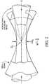
- FIG. 2illustrates the shape of a laser beam in a laser cavity such as in laser 100 . The closer the laser beam is to its diffraction limit in laser material 101 , the greater the depth of field and the smaller the diameter of beam handling optics (for example mirrors 102 and 103 ) required to transmit the beam.
- FIG. 1Cillustrates an end-pumping arrangement for pumping laser material 101 .
- laser material 101is again placed in a laser cavity formed by mirrors 102 and 103 .
- the laser optical energy transmitted through mirror 103is reflected by a dichroic beam splitter 114 to form the beam.
- Optical energy from pump source 116is incident on lens 115 and passes through dichroic beam splitter 114 and mirror 103 to Locus in a nearly diffraction limited region of laser material 101 .
- the beam from pump source 116is reduced to a size and shape that resembles the shape of the laser beam shown in FIG. 2 in active material 101 .
- a second pump source 110can be focused by lens 113 through mirror 102 and into laser material 101 .
- additional optical energycan be coupled into laser material 101 from pump source 111 using a polarizing beam splitting cube 112 , which transmits light from pump source 110 while reflecting light from pump source 111 .
- FIG. 1DA cross section of laser material 101 illustrating optical power concentration is shown in FIG. 1D .
- nearly all of the pump power, as well as the laser beam,is focused in the active region of laser material 101 , where the laser beam produced by laser 117 is produced.
- FIGS. 1E and 1Fshow the photon conversion efficiency (i.e., the number of pump photons versus the number of output laser light photons) with increasing mirror reflectivity at various input optical power densities. Higher mirror reflectivity increases the optical power density within the laser cavity. At higher pump power densities, higher efficiencies result.
- FIG. 1Fshows photon conversion efficiencies as a function of pump power for various spot sizes, which shows the same trend of higher efficiency with optical density as does the graph shown in FIG. 1E .
- Spot sizerefers to the diameter of the optical pump in the optically active laser material.
- Table Ishows typical power usage and lifetime characteristics for a side pumped laser 100 as shown in FIG. 1A , an end-pumped laser 117 as is shown in FIG. 1C , and a lamp pumped laser.
- the diode end-pumped laser 117has the greater efficiency.
- end-pumped laser systemshave more optical components and therefore are difficult to align.
- the optical beam from a laser diode outputsis highly assymmetric. Therefore, light from the diodes is difficult to couple into the active material, e.g. laser material 101 , of an optical amplifier or a laser.
- the lifetimes, efficiency, and expense of various laser diode configurationsmake them very attractive as pump sources for optically active devices.
- Multimode laser diodesare highly desirable optical pump sources as they are inexpensive to manufacture and are capable of producing much higher power levels than single mode lasers. Multimode lasers are more reliable than single-mode lasers as they have lower output power densities reducing the risk of catastrophic facet damage, the primary cause of laser diode failure. However the light emitted by a multimode laser diode is very asymmetric. Typically, the laser diode emitting aperture has dimensions on the order of 1 ⁇ m ⁇ 100 ⁇ m. It is very difficult and costly to collect and couple light emitted by a multimode laser diode into the end facet of a single-mode optical waveguide or fiber.
- waveguide amplifiers and lasersinclude one or more waveguide cores doped with active elements, such as Er, Yb, Nd and Tm, and are designed such that the waveguide can support coaxially propagating single-mode output and pump light.
- the output power of a single-mode, single laser pumped amplifier or laseris often limited to about 20 dBm (100 mW) by the power levels of available single-mode pump lasers.
- Single-mode pump lasersrequire more precision manufacturing tolerances and are consequently more expensive to produce than multimode lasers.
- Complex and costly schemesare required to pump arrays of waveguide optical amplifiers and lasers.
- Pump lighthas to be distributed to each amplifier channel or laser element, requiring combinations of splitters, combiners, taps, monitors and associated control electronics to effectively manage the distribution. Polarization sensitivity of waveguide elements further complicates the distribution process.
- optical laser devicescapable of efficiently coupling light from a laser diode into the active region of a laser cavity that is cost effective and reliable, and that produces high optical output power.
- an optical waveguide devicethat couples light from at least one laser diode into a high refractive index contrast slab waveguide.
- the high refractive index contrast slab waveguideincludes a light duct in a horizontal plane in order to receive light from the at least one laser diode.
- the high refractive index contrast slab waveguideincludes a high refractive index active waveguide and an intermediate refractive index passive cladding.
- the high refractive index contrast slab waveguideis folded in a horizontal axis.
- the intermediate passive claddingis thick enough in the vertical axis to capture a substantial amount of light from the at least one laser diode in the vertical direction.
- light transmitted from the optical waveguide deviceis efficiently coupled into single mode optical fibers by mode size converters.
- FIGS. 1A and 1Billustrate a side-pumped solid-state laser.
- FIGS. 1C and 1Dillustrate an end-pumped solid-state laser.
- FIGS. 1E and 1Fshow graphs illustrating higher pump efficiency with higher optical densities.
- FIG. 2illustrates the characteristics of a typical laser beam in a laser cavity.
- FIGS. 3A and 3Billustrate integration of photodetectors and laser diodes with planar waveguides.
- FIG. 4illustrates a butt-coupling technique for optically coupling between a laser diode and a waveguide.
- FIGS. 5A , 5 B and 5 Cillustrate integrated coupling chips for coupling optical energy from a single mode laser diode chip.
- FIGS. 6A and 6Billustrate a coupling chip for coupling optical energy from a multi-mode laser diode array to a multi-mode optical fiber in accordance with the present invention.
- FIGS. 7A and 7Billustrate a coupling chip for coupling optical energy from a multi-mode laser diode array to a single mode optical fiber in accordance with the present invention.
- FIGS. 8A and 8Billustrate an embodiment of an amplifier chip according to the present invention.
- FIG. 9illustrates the optical materials utilized in waveguides according to the present invention.
- FIGS. 10A , 10 B, and 10 Cillustrate an efficient mode size conversion for vertical pumping of an amplifier core.
- FIG. 11illustrates a monolithic array beam concentrator chip according to the present invention.
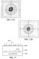
- FIGS. 12A and 12Billustrate the mode images for two example waveguides according to the present invention.
- FIG. 13illustrates a Vertical Cavity Surface Emitting Laser (VCSEL) pumped microchip laser according to the present invention.
- VCSELVertical Cavity Surface Emitting Laser
- Lasers and other light sourceshave great utility when able to produce high optical power densities
- the speed and effectiveness of the interaction of laser power or energy with materialsis in direct proportion to the brightness and intensity of the power or energy that the laser can deliver to the material.
- the highest brightness or intensity of a laser output beamis obtained when the beam is confined to the fundamental, lowest order transverse electromagnetic mode (TEM 00 ). Therefore, single transverse mode is the highest brightness form of a laser's output, which is the laser's most desirable property.
- a high refractive index contrast multimode slab waveguide of an appropriate design to collect and contain a high proportion of the light emitted by a single or multi-element multi-mode pump laser diode and efficiently couple that light into an assembly of actively doped single-mode waveguides embedded within the slabis presented.
- the light from the pump sourcethen, is efficiently coupled into one or more active regions through the effects of the differences in refractive index between the slab material of the waveguide and the cladding material around the slab.
- Both the slab material and the cladding materialcan be deposited with a high degree of uniformity and control in order to obtain the coupling.
- the embedded active core material of the waveguidecan also be manufactured with a high degree of uniformity and control.
- long, single-mode waveguidesare folded many times to accommodate lengths greater than the dimensions of the pumped, encapsulating multimode slab waveguide.
- the single-mode waveguide corescan be folded in such a manner as to optimize the effective absorption cross-section they present to the guided multimode pump light flux while minimizing losses due to bending experienced by propagating single-mode signal light.
- the efficiency of absorption of pump light from the multimode laser diodes by single-mode actively doped waveguide coresis a function of the ratio of the effective cross-section areas of the single-mode and multimode waveguides.
- the multimode slab waveguide itselfis pumped. This effect can result in a slab light source.
- the dimension of the multimode slab waveguideenables conservation of high power densities of the light emitted by the pump laser diode elements, while not increasing the difficulty and reducing the effectiveness of direct coupling between the laser diodes and the edge facet of the slab waveguide.
- High pump power densitiesare particularly important for three-level active systems where natural ground state absorption must first be bleached out before gain can be achieved.
- single-mode light emitted by the laser diode in its fast axis directioni.e., the direction of larger laser beam divergence
- multiple-mode lightimmediately after the light enters a slab waveguide, thereby limiting the return path for pump energy to the pump laser source.
- Lasing and optical amplification processesare processes of energy conversion. Energy is pumped into exciting active elements in the active material, where the energy is stored, from any energy source, commonly optical, which is capable of exciting the active elements. Energy stored in the excited active elements, then, is released when the excited active element is induced by a signal, such as when the active element is perturbed by presence of another photon, into releasing the energy in the form of an optical photon. For example, energy from the excited states of a laser material is released in a highly coherent form by stimulated emission. The efficiency of the conversion process is a key factor in determining the cost-effectiveness of a particular laser or optical amplification or conversion process.
- Planar waveguide forms of optical amplifiers and lasersare desirable as they are very compact compared to other forms of optical amplifiers and lasers.
- a planar waveguide formpotentially allows the integration of diverse optical and electronic functions on, for example, silicon wafers which can be manufactured in high volumes and at low cost with processes commonly used in the semiconductor-industry.
- slab emittersare desirable as efficient light sources.
- FIG. 3Aillustrates integration of an optical waveguide 301 with a photodetector, which may be a photodiode (PD).
- Photodiode 302is formed on semiconducting layer 305 .
- An optical layer 303is formed over photodiode 302 and waveguide 301 is formed on optical layer 303 .
- Light traveling through waveguide 301can be coupled onto photodiode 302 at coupler 306 .
- FIG. 3Billustrates integration of pump laser diodes 310 with an active material waveguide 311 .
- laser waveguide 311is formed on an optical layer 313 .
- Optical layer 313is formed over laser diodes 310 , which are formed on semiconducting layer 312 .
- laser diodes 310can be formed to the side of optical waveguide 311 , over optical waveguide 311 , or in any other orientation with respect to optical waveguide 311 that allows pumping of the active dopant ions of optical waveguide 311 .
- FIG. 4illustrates coupling of a laser diode chip 410 with a high refractive index contrast ( ⁇ n) waveguide 411 .
- the method of coupling illustrated in FIG. 4is referred to as “butt coupling,” where laser diode 410 is a single-mode semiconductor laser diode output facet positioned to within about 5 ⁇ m of high ⁇ n rectangular waveguide 411 in order to correct for mode astigmatism, thereby reducing coupling loss.
- about a 50% couplingcan be achieved with this method utilizing uncoated facets.
- customer demandis for greater than 80-85% coupling efficiency for laser diodes with complex, non-gaussian mode output profiles. Therefore, conventional butt-coupling techniques are not meeting customer demand.
- FIG. 5Aillustrates a laser coupling chip 501 that couples light from a laser diode 506 to an optical fiber 507 .
- Coupling chip 501includes a waveguide 502 with an integrated photodiode 503 to allow for down-stream power monitoring.
- photodiode 503may couple about 0.02 dB to about 0.05 dB of the optical power in waveguide 502 to provide optical coupling.
- a dual-core mode size converter 504can be formed in coupling chip 501 to optimize for efficient optical coupling to optical fiber 507 .
- Dual-core mode size converter 504can couple light to optical fiber with a coupling loss of about 0.25 dB.
- the resulting total loss of less than 1 dB in laser coupling chip 501results in a greater than 80% coupling efficiency between laser diode 506 and optical fiber 507 .
- the coupling efficiency between laser diode 506 and coupling chip 501is less than 80%.
- coupling chip 501can be formed on a millimeter-scale chip sized to fit a standard 14-pin butterfly package. Further, in order to achieve optimum coupling efficiencies, the slow-axis and fast-axis alignment between laser diode 506 and coupling chip 501 requires sub-micron positioning precision.
- FIG. 5Bshows a single mode laser diode array coupler chip 508 .
- Light from laser diode array 520is coupled into waveguides 521 , 522 , 523 , and 524 .
- Waveguides 521 , 522 , 523 and 524are each integrated with a photodetector 525 , 526 , 527 , and 528 , respectively, as is discussed above with regard to FIG. 5A .
- mode size converters 529 , 530 , 531 , and 532formed in waveguides 521 , 522 , 523 , and 524 , respectively, efficiently couple light into optical fibers 533 , 534 , 535 , and 536 , respectively.
- FIG. 5Cshows a single mode laser diode array coupler chip 509 similar to diode array coupler chip 508 with a pitch size converter 540 , which provides for closer packing of optical fibers 533 , 534 , 535 , and 536 .
- the arrangement proposed by Sipesinvolves an array of laser diodes arranged along the corners of a pumping path, for example a zig-zag pattern, such that pump power from multiple laser diodes are coupled into an active waveguide.
- the arrangement proposed by Baerincludes a side pumped active material block with zig-zagging of the signal bea, through the active material for maximum interaction.
- Lawrence Livermore National Labshas proposed a high output Yb:YAG laser system that utilizes a diode bar stack and a lens duct that brings the pump light from the diode bar stack into a Yb:YAG laser rod. About an 80% coupling efficiency can be achieved in this fashion. However, this solution requires a bulk laser rod and a large lens duct to direct light from the diode bar stack into the laser rod.
- Some embodiments of the present inventioncan utilize multimode laser diodes in the form of single elements or arrays, to efficiently pump compact, single-mode, planar waveguide optical amplifiers, lasers, and slab devices, which can be integrated with other optical and electronic functions and manufactured inexpensively in high volumes with semiconductor industry techniques.
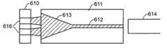
- the output light from a multimode laser diode 610is single-mode in the vertical plane (the fast axis) and multimode in the horizontal plane (the slow axis). Therefore, the output beam diverges very rapidly in the vertical axis (the fast axis) but slowly diverges in the horizontal plane (the slow axis).
- FIGS. 6A and 6Billustrate coupling of light from a laser diode array into a planar waveguide in accordance with the present invention.
- the light beam from laser diodes 616 of multimode laser diode array 610diverges less in the slow axis direction (shown in FIG. 6A ) than it does in the fast axis direction (shown in FIG. 6B ).
- the output beams from laser diode array 610diverge more in the vertical axis (shown in FIG. 6B ) than in the horizontal axis (shown in FIG. 6A ).
- Embodiments of the present inventiontake advantage of the slow divergence in the horizontal axis to increase the optical density in high refractive index waveguide 612 .
- Coupling chip 611can include a large lens duct 613 to direct light into high refractive index waveguide 612 .
- the material of waveguide 612 and lens duct 613can be the same material and can be deposited and patterned on a substrate in the same series of processing steps. Light from waveguide 612 can then be coupled into multimode fiber 614 .
- a higher optical power densitycan be achieved utilizing less expensive multimode laser diode bars, rather than single mode laser diode arrays, and coupling the optical output from multiple ones of the laser diodes in diode array 610 into waveguide 612 .
- Higher coupling efficiencyis achieved by utilizing a light duct 613 formed with waveguide 612 .
- the horizontal alignment between diode array 610 and coupling chip 611is not critical, so long as the light beams are directed toward duct 613 . As shown in FIG. 6B , alignment in the vertical axis (i.e., the fast axis) is somewhat critical because of the large divergence of the light output from diode array 610 in that direction.
- the pump light from the laser diodecan be constrained within the confines of the high ⁇ n slab waveguide and therefore no critical alignment exists between the laser diode and the active waveguide, as would be true for conventional pumping configurations as has been discussed above. Further, there is no need to maintain single-mode propagation in the horizontal direction, as alignment tolerance are relaxed in the horizontal plane. In the vertical plane, a single optical mode can be excited to obtain maximum power density by using more precise alignment. When maximize power density is not required, the alignment tolerances in the vertical plane can also be relieved by using a thicker high refractive index contrast slab waveguide and allowing the light to propagate multimode in the vertical direction as well.
- FIGS. 7A and 7Billustrate coupling utilizing a double-clad core.
- light from one or more laser diodes 710 of multimode pump diode array 702is coupled into waveguide 703 of coupling chip 701 .
- a lens duct 704can be formed with waveguide 703 to direct light from laser diodes 710 in diode array 702 into waveguide 703 .
- light from waveguide 703can be coupled into single-mode fiber 705 .
- FIG. 7Bshows a cross-section of waveguide 703 .
- Waveguide 703includes a single-mode core 706 .
- Single-mode core 706can be formed, for example, from rare-earth doped Al 2 O 3 , Y 2 O 3 , or TiO 2 to form a high refractive index core.
- Single-mode core 706can be surrounded by a multi-mode cladding 707 having a lower refractive index than that of single-mode core 706 , which can be formed from an intermediate refractive index contrast material such as Al 2 O 3 or Y 2 O 3 .
- the dimensions of multi-mode cladding 707can capture most or all of the light output from laser diode array 702 .
- Waveguide 703can be formed on, for example, a silica or aluminosilicate buffer layer 709 deposited on a substrate.
- a second buffer layer 708can be formed over waveguide 703 .
- coupling chip 701can provide efficient conversion of low optical power density light emitted from directly-coupled multimode laser diode bars to high optical power density.
- high-refractive index contrast core 706is optically active
- a lasercan be formed by including a laser cavity, which can be formed by depositing mirrors on the ends of chip 701 .
- Very high optical-to-optical efficienciescan be achieved in coupling chip 701 .
- a multimode laser diode operating at a wavelength of 920 nmis efficiently coupled into a single-mode output laser at about 1100 nm utilizing an active waveguide 706 formed from double-clad Yb-doped silica, for example.
- a single mode active waveguide located in the high refractive index portion of the slabwill be efficiently pumped.
- Such active areasare shown, for example, in FIGS. 8A and 8B .
- the active region of the waveguidecan be “folded” or routed through many loops in order to increase the length of active material pumped and thereby increase the amplification in the waveguide.
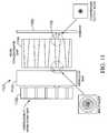
- FIGS. 8A and 8BAn embodiment of a folded active region embedded within the large high refractive index slab is shown in FIGS. 8A and 8B .
- any appropriate configuration or routing of active area waveguide within the slabcan be utilized.
- zig-zag configurationsmay also be utilized in addition to the spiral configuration shown in FIG. 8A .
- linear arrays of active regionsmay be utilized.
- FIG. 8Ashows the slow axis view (i.e., the horizontal view) and FIG. 8B shows the fast-axis view (i.e., the vertical cross section) of an active waveguide amplifier or laser chip 801 pumped by a multimode laser diode array in accordance with the present invention.
- a single mode high refractive index contrast core 803is arranged on chip 801 .
- a spiral arrangementis shown in FIG. 8A , any arrangement that provides a long signal path between a single mode input fiber 807 and a single mode output fiber 808 can be implemented.
- FIG. 8Bshows a cross section of an area of chip 801 with multiple crossings of single-mode high refractive index contrast active waveguide 803 .
- active waveguide 803can be formed from Yb-doped Al 2 O 3 , Y 2 O 3 or TiO 2 .
- Intermediate refractive index contrast cladding 804can be formed from Al 2 O 3 or Y 2 O 3 . In this arrangement, a high pump-power density can be achieved in multi-mode cladding 804 , which results in highly efficient pumping of active waveguide 803 .
- Cladding 804may be surrounded by layers 805 and 806 .
- Multi-port amplifierscan be obtained by routing multiple folded regions of active waveguide such as waveguide 803 within the high ⁇ n slab 804 of chip 801 .
- multiple active coresmay be routed together as shown in FIG. 8A .
- a single multimode pumptherefore, can be shared among several single-mode active amplifying waveguides without the need to split the pump light and separately distribute the light to activate the single-mode amplifying waveguides separately. There is, therefore, no need for pump splitters or multiplexers. Further, the higher area of the active region increases absorption of the pump light, reducing the need for mirrors to rout the pump light through the active regions multiple times.
- FIG. 9illustrates material depositions that provide high grade, optically transparent, highly uniform slab waveguides with highly controllable ⁇ n values.
- the production of such waveguidesis further discussed in U.S. application Ser. No. 09/903,081, “As-Deposited Optical Waveguides with Low Scattering Loss and Methods for Their Manufacture,” by Demaray et al, filed on Jul. 10, 2001; U.S. application Ser. No. 10/101,863, “Biased Pulse DC Sputtering of Oxide Films, by Zhang et al., filed on Mar. 16, 2002; U.S. application Ser. No.
- Waveguide materials used to form active core waveguides, passive waveguides, and claddings consistent with embodiments of the present inventioncan be deposited by biased pulsed DC plasma vapor deposition (PVD), as described in U.S. application Ser. No. 10/101,341 (the '341 application).
- the physical characteristics of the optical material deposited by biased pulsed DC PVDdepends on various process parameters, as discussed in the '341 application.
- a device, including photodetectors and other electronics, such as those shown in FIGS. 3A through 8B and discussed above,can be fabricated by depositing one or more active or passive optical layers and patterning the optical layers to form the waveguides and lens ducts as shown. In some applications, several deposition and patterning steps may be applied to form the desired structures.
- FIG. 9which shows active and passive waveguide materials of highly amorphous, defect free films of aluminasilicated deposited by biased pulsed DC PVD.
- the filmshave very high optical transparency, for example below 0.3 db/cm loss and, in some deposited films, less than about 0.1 db/cm loss. Therefore, deposition of films utilizing biased pulsed-DC PVD are useful for providing structures for optical coupling devices, optical amplifiers, and optical laser structures for highly efficient coupling of pump sources as has been discussed above.
- depositionis performed in a vacuum deposition chamber.
- a substrateis mounted on a support which also provides an RF bias voltage to the substrate.
- RF poweris supplied to a target formed from material to be deposited as gas is allowed into the chamber.
- a plasmais excited in the gas and the material is deposited on the substrate.
- a pulsed DC signalis provided to the target. Further details regarding the deposition process are provided in the '341 application.
- FIGS. 10A , 10 B, and 10 CCoupling of light, for example from optical fiber 807 into waveguide 803 , through efficient mode size conversion is illustrated in FIGS. 10A , 10 B, and 10 C.
- Vertically tapered mode-size conversionis further discussed in U.S. application Ser. No. 10/101,492, “Mode Size Converter for a Planar Waveguide,” by Tao et al, filed on Mar. 16, 2002, herein incorporated by reference in its entirety.
- a very smooth vertical tapercan efficiently couple light from optical fiber 807 into high refractive index contrast, core waveguide 803 very efficiently.
- FIG. 10Bshows the mode size of an optical beam at a point where light enters waveguide 803 .
- FIG. 10Bshows a significantly smaller mode size in the region of waveguide 803 after the adiabatic S-taper mode size converter 1001 .
- Mode size converter 1001can be produced in a biased pulsed-DC PVD process with a shadow mask.
- Table IIshows modeling of mode diameter at the output facet of a mode converter for various core/cladding refractive index contrasts ⁇ n.
- the dimensions in Table IIrefer to the dimensions of the output facet of the rectangular mode converter.
- FIG. 11illustrates an image concentrator 1101 for adiabatically compressing the diameter of the mode output by a passively Q-switched microchip laser array.
- Image concentrator 1101employs a reverse taper 1106 , such as that first disclosed in U.S. application Ser. No. 10/101,492 to Tao et al.
- Reverse taper 1106can be formed vertically and/or horizontally and thereby provides coupling into a smaller mode size.
- a further embodimentincludes a pitch size conversion such as that illustrated in FIG. 5C .
- Embodiments of the inventionenable the mode size and pitch size conversion of individually addressable microchip laser array, so as to be tailored to standard print pixel densities for use in direct printing and micromaching applications.
- Image concentrator 1101can include an addressable array pump bar 1102 which is capable of addressing and exciting individual pixels of a microchip bar 1103 .
- Array pump bar 1102includes an array of laser diodes which produce light when individually addressed.
- Microchip bar 1103which provides amplification as was discussed in FIGS. 6-8 .
- Beam concentrator chip 1104can include light ducts or vertical tapers in order to collect a substantial amount of light from microchip bar 1103 . Further, a vertical reverse taper 1106 , as is described in U.S. application Ser. No. 10/101,492, allows for a compressed output mode. As shown in FIG. 11 , the mode of the beam output by beam concentrator chip 1104 is much smaller than the mode of the beam in microchip bar 1103 .
- a monolithic array beam concentrator chipcan convert 50 ⁇ m or 90 ⁇ m diameter single mode spots from microchip bar 1103 into 20 to 25 ⁇ m diameter spots on window 1105 .
- FIGS. 12A and 12Bshow mode sizes for some weakly-confined mode propagation in waveguides.
- FIG. 12Aillustrates a 6.2 ⁇ m mode diameter at the output facet of a 1.5 ⁇ m ⁇ 3.5 ⁇ m waveguide for 980 nm light with a refractive index contrast ⁇ n between the core and the cladding of about 1%.
- FIG. 12Billustrates a 7.6 ⁇ m mode diameter at the output facet of a 1.25 ⁇ m ⁇ 3.5 ⁇ m waveguide for 980 nm light with a refractive index contrast of about 1%.
- the optical energyis concentrated in the center of the facet.
- Table IIIillustrates facet damage considerations in a image concentrator such as image concentrator 1101 shown in FIG. 11 .
- Table IIIillustrates, for representative pixel densities, the mode size required, the distance between modes, and the resulting power density in image concentrator 1101 .
- the value of 14.2 for power density shown for 2400 dpi pixel densityexceeds the damage threshold of Quartz.
- FIG. 13illustrates a vertical cavity surface emitting laser (VCSEL)-pumped microchip 1401 according to the present invention.
- VCSELs 1403can be deposited on a GaAs substrate 1402 .
- VCSELs 1403include a dichroic output facet coating.
- An active gain medium 1404can be deposited directly over VCSELs 1403 .
- Active gain medium 1404can be, for example, Nd, Yb, Er, Tm, Ho, Pr, or Ce doped silica.
- a saturable absorber 1405can be deposited over gain medium 1404 .
- Saturable absorber 1405can be, for example, a Cr4+ or Co2+ doped silica film.
- a VCSEL pumped microchip 1401can be fabricated using high volume wafer-scale semiconductor manufacturing techniques.
- the doped silica used for saturable absorber 1405 and active gain medium 1404can be deposited by biased pulsed-DC PVD processing techniques.
Landscapes
- Physics & Mathematics (AREA)
- Optics & Photonics (AREA)
- Engineering & Computer Science (AREA)
- Electromagnetism (AREA)
- General Physics & Mathematics (AREA)
- Plasma & Fusion (AREA)
- Microelectronics & Electronic Packaging (AREA)
- Lasers (AREA)
- Optical Couplings Of Light Guides (AREA)
Abstract
Description
| TABLE I | ||||
| Lamp | Diode End- | Diode Side- | ||
| Pumped | Pumped | Pumped | ||
| Power to Pump | 5000 | W | 2.5 | W | 50 | W |
| Source | ||||||
| Power to Cooling | 500 | W | 2.5 | W | 50 | W |
| System | ||||||
| Power from Pump | 3500 | W | 1.25 | W | 20 | W |
| Source | ||||||
| Single-Mode | 10 | W | 0.8 | W | 10 | W |
| Power from Laser |
| Wall-Plug Effi- | 0.2% | 16% | 10% |
| ciency | |||
| Cooling | Water | Free Air | Forced Air |
| Power Consumed/ | 500 | kW-hr | 6.5 | kW-hr | 10 | kW-hr |
| Output kW-hr |
| Cost of Light | $200 | $400 | $1000 |
| Source |
| Lifetime of Light | 200 | hrs | 20,000 | hrs | 10,000 | hrs |
| Source | ||||||
| TABLE II | ||||
| 1.0 μm × | 1.5 μm × | |||
| Δn | 1.0 μm | 1.5 μm | 2.0 μm × 2.0 μm | 2.5 μm × 2.5 μm |
| 0.43% | 38 μm | 35 μm | 14 μm | 6 μm |
| 0.3% | 36 μm | 20 μm | 16 μm | |
| 0.2% | 32 μm | 24 μm | ||
| TABLE III | |||
| Pixel | |||
| Density | Mode Pitch/Mode | Power Density at | Collimation Distance |
| (dpi) | Size | Facet (GW cm−2) | (μm) |
| 600 | 42 | 0.9 | 842 |
| 1200 | 21 | 3.6 | 210 |
| 2400 | 11 | 14.2 | 53 |
Claims (17)
Priority Applications (1)
| Application Number | Priority Date | Filing Date | Title |
|---|---|---|---|
| US10/650,461US7826702B2 (en) | 2002-08-27 | 2003-08-27 | Optically coupling into highly uniform waveguides |
Applications Claiming Priority (2)
| Application Number | Priority Date | Filing Date | Title |
|---|---|---|---|
| US40645102P | 2002-08-27 | 2002-08-27 | |
| US10/650,461US7826702B2 (en) | 2002-08-27 | 2003-08-27 | Optically coupling into highly uniform waveguides |
Publications (2)
| Publication Number | Publication Date |
|---|---|
| US20040105644A1 US20040105644A1 (en) | 2004-06-03 |
| US7826702B2true US7826702B2 (en) | 2010-11-02 |
Family
ID=31978302
Family Applications (1)
| Application Number | Title | Priority Date | Filing Date |
|---|---|---|---|
| US10/650,461Expired - Fee RelatedUS7826702B2 (en) | 2002-08-27 | 2003-08-27 | Optically coupling into highly uniform waveguides |
Country Status (4)
| Country | Link |
|---|---|
| US (1) | US7826702B2 (en) |
| AU (1) | AU2003261463A1 (en) |
| TW (1) | TWI274199B (en) |
| WO (1) | WO2004021532A1 (en) |
Cited By (15)
| Publication number | Priority date | Publication date | Assignee | Title |
|---|---|---|---|---|
| US20060057304A1 (en)* | 2002-03-16 | 2006-03-16 | Symmorphix, Inc. | Biased pulse DC reactive sputtering of oxide films |
| US20110002694A1 (en)* | 2009-07-01 | 2011-01-06 | Hokuyo Automatic Co., Ltd. | Optical data transmission apparatus |
| US8045832B2 (en) | 2002-03-16 | 2011-10-25 | Springworks, Llc | Mode size converter for a planar waveguide |
| US8636876B2 (en) | 2004-12-08 | 2014-01-28 | R. Ernest Demaray | Deposition of LiCoO2 |
| US8728285B2 (en) | 2003-05-23 | 2014-05-20 | Demaray, Llc | Transparent conductive oxides |
| US9196278B1 (en)* | 2014-05-23 | 2015-11-24 | Seagate Technology Llc | Laser array for heat assisted magnetic recording |
| US9325140B2 (en) | 2013-03-14 | 2016-04-26 | Massachusetts Institute Of Technology | Photonic devices and methods of using and making photonic devices |
| US9366816B2 (en) | 2012-11-12 | 2016-06-14 | Demaray, Llc | Adiabatic planar waveguide coupler transformer |
| US9515739B2 (en) | 2011-06-01 | 2016-12-06 | Arris Enterprises, Inc. | Mitigating noise and OBI in RFoG networks |
| EP3407106A4 (en)* | 2016-03-09 | 2019-05-08 | Huawei Technologies Co., Ltd. | OPTICAL COUPLING CONNECTOR, OPTICAL COUPLING SYSTEM, AND WAVEGUIDE COUPLING METHOD |
| US20190160301A1 (en)* | 2016-04-29 | 2019-05-30 | Lutronic Corporation | Laser beam device and laser beam hand piece |
| US10732265B1 (en) | 2019-04-11 | 2020-08-04 | Analog Devices, Inc. | Optical illuminator module and related techniques |
| US10818909B2 (en) | 2016-05-09 | 2020-10-27 | Demaray, Llc | Energy storage device with a first metal layer formed from a precursor layer upon charge and diffused into a cathode during discharge |
| US20210262854A1 (en)* | 2014-06-09 | 2021-08-26 | Unm Rainforest Innovations | Integrated bound-mode spectral/angular sensors |
| US11808997B1 (en)* | 2022-09-19 | 2023-11-07 | Nexus Photonics Inc. | Heterogeneous photonic integrated circuits with doped waveguides |
Families Citing this family (52)
| Publication number | Priority date | Publication date | Assignee | Title |
|---|---|---|---|---|
| US7469558B2 (en) | 2001-07-10 | 2008-12-30 | Springworks, Llc | As-deposited planar optical waveguides with low scattering loss and methods for their manufacture |
| US7404877B2 (en) | 2001-11-09 | 2008-07-29 | Springworks, Llc | Low temperature zirconia based thermal barrier layer by PVD |
| US20030175142A1 (en)* | 2002-03-16 | 2003-09-18 | Vassiliki Milonopoulou | Rare-earth pre-alloyed PVD targets for dielectric planar applications |
| US8236443B2 (en) | 2002-08-09 | 2012-08-07 | Infinite Power Solutions, Inc. | Metal film encapsulation |
| US7993773B2 (en) | 2002-08-09 | 2011-08-09 | Infinite Power Solutions, Inc. | Electrochemical apparatus with barrier layer protected substrate |
| US8394522B2 (en) | 2002-08-09 | 2013-03-12 | Infinite Power Solutions, Inc. | Robust metal film encapsulation |
| US8021778B2 (en) | 2002-08-09 | 2011-09-20 | Infinite Power Solutions, Inc. | Electrochemical apparatus with barrier layer protected substrate |
| US8445130B2 (en) | 2002-08-09 | 2013-05-21 | Infinite Power Solutions, Inc. | Hybrid thin-film battery |
| US8404376B2 (en) | 2002-08-09 | 2013-03-26 | Infinite Power Solutions, Inc. | Metal film encapsulation |
| US20070264564A1 (en) | 2006-03-16 | 2007-11-15 | Infinite Power Solutions, Inc. | Thin film battery on an integrated circuit or circuit board and method thereof |
| US8431264B2 (en) | 2002-08-09 | 2013-04-30 | Infinite Power Solutions, Inc. | Hybrid thin-film battery |
| US7826702B2 (en) | 2002-08-27 | 2010-11-02 | Springworks, Llc | Optically coupling into highly uniform waveguides |
| WO2004077519A2 (en) | 2003-02-27 | 2004-09-10 | Mukundan Narasimhan | Dielectric barrier layer films |
| US7238628B2 (en)* | 2003-05-23 | 2007-07-03 | Symmorphix, Inc. | Energy conversion and storage films and devices by physical vapor deposition of titanium and titanium oxides and sub-oxides |
| GB2416241B (en)* | 2004-07-14 | 2009-09-30 | Agilent Technologies Inc | Improved low cost optical amplifier |
| US7959769B2 (en) | 2004-12-08 | 2011-06-14 | Infinite Power Solutions, Inc. | Deposition of LiCoO2 |
| JP4257926B2 (en) | 2005-04-19 | 2009-04-30 | 協和発酵キリン株式会社 | Nitrogen-containing heterocyclic compounds |
| US7838133B2 (en) | 2005-09-02 | 2010-11-23 | Springworks, Llc | Deposition of perovskite and other compound ceramic films for dielectric applications |
| US7313299B2 (en)* | 2006-03-09 | 2007-12-25 | Lockheed Martin Coherent Technologies, Inc. | Laser beam transformation and combination using tapered waveguides |
| US9528939B2 (en) | 2006-03-10 | 2016-12-27 | Indx Lifecare, Inc. | Waveguide-based optical scanning systems |
| US9423397B2 (en) | 2006-03-10 | 2016-08-23 | Indx Lifecare, Inc. | Waveguide-based detection system with scanning light source |
| US9976192B2 (en) | 2006-03-10 | 2018-05-22 | Ldip, Llc | Waveguide-based detection system with scanning light source |
| US7474815B2 (en)* | 2006-03-14 | 2009-01-06 | International Business Machines Corporation | Interconnecting (mapping) a two-dimensional optoelectronic (OE) device array to a one-dimensional waveguide array |
| JP2010505044A (en) | 2006-09-29 | 2010-02-18 | インフィニット パワー ソリューションズ, インコーポレイテッド | Material constraints for masking flexible substrates and depositing battery layers on flexible substrates |
| WO2008047831A1 (en) | 2006-10-17 | 2008-04-24 | Kyowa Hakko Kirin Co., Ltd. | Jak inhibitor |
| US8197781B2 (en) | 2006-11-07 | 2012-06-12 | Infinite Power Solutions, Inc. | Sputtering target of Li3PO4 and method for producing same |
| DE202007017386U1 (en)* | 2007-12-13 | 2008-02-28 | CCS Technology, Inc., Wilmington | Coupling device for coupling optical waveguides |
| US7693373B2 (en)* | 2007-12-18 | 2010-04-06 | Analog Devices, Inc. | Bidirectional optical link over a single multimode fiber or waveguide |
| US9334557B2 (en) | 2007-12-21 | 2016-05-10 | Sapurast Research Llc | Method for sputter targets for electrolyte films |
| US8268488B2 (en) | 2007-12-21 | 2012-09-18 | Infinite Power Solutions, Inc. | Thin film electrolyte for thin film batteries |
| JP5705549B2 (en) | 2008-01-11 | 2015-04-22 | インフィニット パワー ソリューションズ, インコーポレイテッド | Thin film encapsulation for thin film batteries and other devices |
| US8350519B2 (en) | 2008-04-02 | 2013-01-08 | Infinite Power Solutions, Inc | Passive over/under voltage control and protection for energy storage devices associated with energy harvesting |
| GB2461026B (en)* | 2008-06-16 | 2011-03-09 | Plc Diagnostics Inc | System and method for nucleic acids sequencing by phased synthesis |
| WO2010019577A1 (en) | 2008-08-11 | 2010-02-18 | Infinite Power Solutions, Inc. | Energy device with integral collector surface for electromagnetic energy harvesting and method thereof |
| JP5650646B2 (en) | 2008-09-12 | 2015-01-07 | インフィニット パワー ソリューションズ, インコーポレイテッド | Energy device with integral conductive surface for data communication via electromagnetic energy and method for data communication via electromagnetic energy |
| WO2010042594A1 (en)* | 2008-10-08 | 2010-04-15 | Infinite Power Solutions, Inc. | Environmentally-powered wireless sensor module |
| KR20120035912A (en)* | 2009-04-29 | 2012-04-16 | 피엘씨 다이아그노스틱스, 인크. | Waveguide-based detection system with scanning light source |
| WO2011028825A1 (en) | 2009-09-01 | 2011-03-10 | Infinite Power Solutions, Inc. | Printed circuit board with integrated thin film battery |
| JP5435476B2 (en)* | 2010-01-15 | 2014-03-05 | 古河電気工業株式会社 | Multi-core optical fiber manufacturing method |
| KR101930561B1 (en) | 2010-06-07 | 2018-12-18 | 사푸라스트 리써치 엘엘씨 | Rechargeable high-density electrochemical device |
| US8971376B2 (en)* | 2010-08-06 | 2015-03-03 | Kaiam Corp. | Broad area laser pump combiner |
| DE102010047917A1 (en)* | 2010-10-08 | 2012-04-12 | Jenoptik Automatisierungstechnik Gmbh | Device for simultaneous circumferential machining of a workpiece with laser beams |
| US20120289799A1 (en)* | 2011-05-13 | 2012-11-15 | Kestrel Labs, Inc. | High-Throughput Alignment-Insensitive Optical Connector for Laser-Based Photoplethysmography |
| DE102012100408B4 (en)* | 2012-01-19 | 2013-08-14 | Carl Zeiss Meditec Ag | A coupling device for coupling light from a light emitting diode into a fiber inlet end and light source arrangement equipped therewith |
| US20130236193A1 (en)* | 2012-03-09 | 2013-09-12 | Commscope, Inc. Of North Carolina | Optical Communications Systems that Couple Optical Signals from a Large Core Fiber to a Smaller Core Fiber and Related Methods and Apparatus |
| US10371890B2 (en) | 2013-02-26 | 2019-08-06 | Furukawa Electric Co., Ltd. | Optical waveguide element |
| US10018566B2 (en) | 2014-02-28 | 2018-07-10 | Ldip, Llc | Partially encapsulated waveguide based sensing chips, systems and methods of use |
| JP2016038395A (en)* | 2014-08-05 | 2016-03-22 | 日東電工株式会社 | Method of light incident upon optical waveguide |
| US11181479B2 (en) | 2015-02-27 | 2021-11-23 | Ldip, Llc | Waveguide-based detection system with scanning light source |
| US10908286B2 (en) | 2017-09-29 | 2021-02-02 | Intel Corporation | Integrated optical transmitter and receiver |
| US10976496B2 (en)* | 2019-02-11 | 2021-04-13 | Poet Technologies, Inc. | Dual core waveguide |
| CN116106862B (en)* | 2023-04-10 | 2023-08-04 | 深圳市速腾聚创科技有限公司 | Optical chip, laser radar, automatic driving system and movable equipment |
Citations (221)
| Publication number | Priority date | Publication date | Assignee | Title |
|---|---|---|---|---|
| US3309302A (en) | 1963-10-07 | 1967-03-14 | Varian Associates | Method of preparing an electron tube including sputtering a suboxide of titanium on dielectric components thereof |
| US3616403A (en) | 1968-10-25 | 1971-10-26 | Ibm | Prevention of inversion of p-type semiconductor material during rf sputtering of quartz |
| US3850604A (en) | 1972-12-11 | 1974-11-26 | Gte Laboratories Inc | Preparation of chalcogenide glass sputtering targets |
| US4082569A (en) | 1977-02-22 | 1978-04-04 | The United States Of America As Represented By The Administrator Of The National Aeronautics And Space Administration | Solar cell collector |
| US4111523A (en) | 1973-07-23 | 1978-09-05 | Bell Telephone Laboratories, Incorporated | Thin film optical waveguide |
| US4437966A (en) | 1982-09-30 | 1984-03-20 | Gte Products Corporation | Sputtering cathode apparatus |
| US4587225A (en) | 1983-10-17 | 1986-05-06 | Toyo Soda Manufacturing Co., Ltd. | High-strength zirconia type sintered body |
| US4619680A (en) | 1984-06-11 | 1986-10-28 | The General Electric Co. P.L.C. | Manufacture of integrated optical waveguides |
| USRE32499E (en) | 1980-05-08 | 1987-09-08 | University Of South Florida | Method for quantitative analysis for limonin |
| US4710940A (en) | 1985-10-01 | 1987-12-01 | California Institute Of Technology | Method and apparatus for efficient operation of optically pumped laser |
| US4785459A (en) | 1985-05-01 | 1988-11-15 | Baer Thomas M | High efficiency mode matched solid state laser with transverse pumping |
| DE3738738C1 (en) | 1987-11-14 | 1989-01-26 | Degussa | Powder-metallurgical process for producing targets |
| US4915810A (en) | 1988-04-25 | 1990-04-10 | Unisys Corporation | Target source for ion beam sputter deposition |
| US4978437A (en) | 1984-05-12 | 1990-12-18 | Leybold Aktiengesellschaft | Method of applying optical coatings of silicon compounds by cathode sputtering, and a sputtering cathode for the practice of the method |
| US5085904A (en) | 1990-04-20 | 1992-02-04 | E. I. Du Pont De Nemours And Company | Barrier materials useful for packaging |
| US5107538A (en) | 1991-06-06 | 1992-04-21 | At&T Bell Laboratories | Optical waveguide system comprising a rare-earth Si-based optical device |
| US5119460A (en) | 1991-04-25 | 1992-06-02 | At&T Bell Laboratories | Erbium-doped planar optical device |
| US5173271A (en) | 1985-12-04 | 1992-12-22 | Massachusetts Institute Of Technology | Enhanced radiative zone-melting recrystallization method and apparatus |
| US5174876A (en) | 1989-12-18 | 1992-12-29 | Forschungszentrum Julich Gmbh | Method of making an optical component by ion implantation |
| US5196041A (en) | 1991-09-17 | 1993-03-23 | The Charles Stark Draper Laboratory, Inc. | Method of forming an optical channel waveguide by gettering |
| US5200029A (en) | 1991-04-25 | 1993-04-06 | At&T Bell Laboratories | Method of making a planar optical amplifier |
| US5206925A (en) | 1990-06-29 | 1993-04-27 | Hitachi Cable Limited | Rare earth element-doped optical waveguide and process for producing the same |
| US5225288A (en) | 1990-08-10 | 1993-07-06 | E. I. Du Pont De Nemours And Company | Solvent blockers and multilayer barrier coatings for thin films |
| US5237439A (en) | 1991-09-30 | 1993-08-17 | Sharp Kabushiki Kaisha | Plastic-substrate liquid crystal display device with a hard coat containing boron or a buffer layer made of titanium oxide |
| US5252194A (en) | 1990-01-26 | 1993-10-12 | Varian Associates, Inc. | Rotating sputtering apparatus for selected erosion |
| US5287427A (en) | 1992-05-05 | 1994-02-15 | At&T Bell Laboratories | Method of making an article comprising an optical component, and article comprising the component |
| US5296089A (en) | 1985-12-04 | 1994-03-22 | Massachusetts Institute Of Technology | Enhanced radiative zone-melting recrystallization method and apparatus |
| US5303319A (en) | 1992-12-28 | 1994-04-12 | Honeywell Inc. | Ion-beam deposited multilayer waveguides and resonators |
| US5306569A (en) | 1990-06-15 | 1994-04-26 | Hitachi Metals, Ltd. | Titanium-tungsten target material and manufacturing method thereof |
| US5309302A (en) | 1990-12-21 | 1994-05-03 | U.S. Philips Corporation | System comprising a player and/or recorder apparatus and a tape cassette, and the apparatus and a cassette suitable for use in such a system |
| US5338625A (en) | 1992-07-29 | 1994-08-16 | Martin Marietta Energy Systems, Inc. | Thin film battery and method for making same |
| US5355089A (en) | 1992-07-22 | 1994-10-11 | Duracell Inc. | Moisture barrier for battery with electrochemical tester |
| US5362672A (en) | 1988-06-17 | 1994-11-08 | Tadahiro Ohmi | Method of forming a monocrystalline film having a closed loop step portion on the substrate |
| US5381262A (en) | 1992-08-18 | 1995-01-10 | Fujitsu Limited | Planar wave guide type optical amplifier |
| EP0639655A1 (en) | 1993-07-28 | 1995-02-22 | Asahi Glass Company Ltd. | Method and apparatus for sputtering |
| EP0652308A2 (en) | 1993-10-14 | 1995-05-10 | Neuralsystems Corporation | Method of and apparatus for forming single-crystalline thin film |
| US5427669A (en) | 1992-12-30 | 1995-06-27 | Advanced Energy Industries, Inc. | Thin film DC plasma processing system |
| US5435826A (en) | 1992-11-24 | 1995-07-25 | Hitachi Metals, Ltd. | Sputtering target and method for producing same |
| US5457569A (en) | 1994-06-30 | 1995-10-10 | At&T Ipm Corp. | Semiconductor amplifier or laser having integrated lens |
| US5472795A (en) | 1994-06-27 | 1995-12-05 | Board Of Regents Of The University Of The University Of Wisconsin System, On Behalf Of The University Of Wisconsin-Milwaukee | Multilayer nanolaminates containing polycrystalline zirconia |
| US5475528A (en) | 1994-03-25 | 1995-12-12 | Corning Incorporated | Optical signal amplifier glasses |
| US5478456A (en) | 1993-10-01 | 1995-12-26 | Minnesota Mining And Manufacturing Company | Sputtering target |
| US5483613A (en) | 1994-08-16 | 1996-01-09 | At&T Corp. | Optical device with substrate and waveguide structure having thermal matching interfaces |
| US5499207A (en) | 1993-08-06 | 1996-03-12 | Hitachi, Ltd. | Semiconductor memory device having improved isolation between electrodes, and process for fabricating the same |
| US5538796A (en) | 1992-10-13 | 1996-07-23 | General Electric Company | Thermal barrier coating system having no bond coat |
| WO1996023085A1 (en) | 1995-01-25 | 1996-08-01 | Applied Komatsu Technology, Inc. | Autoclave bonding of sputtering target assembly |
| US5555127A (en) | 1994-06-30 | 1996-09-10 | The Whitaker Corporation | Planar hybrid optical amplifier |
| US5561004A (en) | 1994-02-25 | 1996-10-01 | Bates; John B. | Packaging material for thin film lithium batteries |
| US5563979A (en) | 1995-08-31 | 1996-10-08 | Lucent Technologies Inc. | Erbium-doped planar optical device |
| US5565071A (en) | 1993-11-24 | 1996-10-15 | Applied Materials, Inc. | Integrated sputtering target assembly |
| US5569520A (en) | 1994-01-12 | 1996-10-29 | Martin Marietta Energy Systems, Inc. | Rechargeable lithium battery for use in applications requiring a low to high power output |
| US5591520A (en) | 1991-12-11 | 1997-01-07 | Mobil Oil Corporation | High barrier film |
| US5603816A (en) | 1993-11-24 | 1997-02-18 | Applied Materials, Inc. | Sputtering device and target with cover to hold cooling fluid |
| US5607789A (en) | 1995-01-23 | 1997-03-04 | Duracell Inc. | Light transparent multilayer moisture barrier for electrochemical cell tester and cell employing same |
| US5607560A (en) | 1993-03-25 | 1997-03-04 | Canon Kabushiki Kaisha | Diamond crystal forming method |
| US5613995A (en) | 1993-04-23 | 1997-03-25 | Lucent Technologies Inc. | Method for making planar optical waveguides |
| US5645626A (en) | 1990-08-10 | 1997-07-08 | Bend Research, Inc. | Composite hydrogen separation element and module |
| US5654984A (en) | 1993-12-03 | 1997-08-05 | Silicon Systems, Inc. | Signal modulation across capacitors |
| US5654054A (en) | 1992-12-18 | 1997-08-05 | Becton, Dickinson And Company | Barrier coating |
| WO1997035044A1 (en) | 1996-03-22 | 1997-09-25 | Materials Research Corporation | Method and apparatus for rf diode sputtering |
| US5686360A (en) | 1995-11-30 | 1997-11-11 | Motorola | Passivation of organic devices |
| US5689522A (en) | 1995-10-02 | 1997-11-18 | The Regents Of The University Of California | High efficiency 2 micrometer laser utilizing wing-pumped Tm3+ and a laser diode array end-pumping architecture |
| US5693956A (en) | 1996-07-29 | 1997-12-02 | Motorola | Inverted oleds on hard plastic substrate |
| US5702829A (en) | 1991-10-14 | 1997-12-30 | Commissariat A L'energie Atomique | Multilayer material, anti-erosion and anti-abrasion coating incorporating said multilayer material |
| EP0820088A2 (en) | 1996-07-19 | 1998-01-21 | Applied Komatsu Technology, Inc. | Non-planar magnet tracking device for magnetron sputtering apparatus |
| US5718813A (en) | 1992-12-30 | 1998-02-17 | Advanced Energy Industries, Inc. | Enhanced reactive DC sputtering system |
| US5719976A (en) | 1995-10-24 | 1998-02-17 | Lucent Technologies, Inc. | Optimized waveguide structure |
| US5731661A (en) | 1996-07-15 | 1998-03-24 | Motorola, Inc. | Passivation of electroluminescent organic devices |
| US5738731A (en) | 1993-11-19 | 1998-04-14 | Mega Chips Corporation | Photovoltaic device |
| US5755938A (en) | 1993-08-24 | 1998-05-26 | Alps Electric Co., Ltd. | Single chamber for CVD and sputtering film manufacturing |
| US5761234A (en)* | 1996-07-09 | 1998-06-02 | Sdl, Inc. | High power, reliable optical fiber pumping system with high redundancy for use in lightwave communication systems |
| US5762768A (en) | 1995-08-18 | 1998-06-09 | W.C. Heraeus Gmbh | Target for cathodic sputtering and method for producing the target |
| US5771562A (en) | 1995-05-02 | 1998-06-30 | Motorola, Inc. | Passivation of organic devices |
| US5789071A (en) | 1992-11-09 | 1998-08-04 | Northwestern University | Multilayer oxide coatings |
| US5792550A (en) | 1989-10-24 | 1998-08-11 | Flex Products, Inc. | Barrier film having high colorless transparency and method |
| US5811177A (en) | 1995-11-30 | 1998-09-22 | Motorola, Inc. | Passivation of electroluminescent organic devices |
| US5831262A (en) | 1997-06-27 | 1998-11-03 | Lucent Technologies Inc. | Article comprising an optical fiber attached to a micromechanical device |
| US5830330A (en) | 1997-05-22 | 1998-11-03 | Tokyo Electron Limited | Method and apparatus for low pressure sputtering |
| US5841931A (en) | 1996-11-26 | 1998-11-24 | Massachusetts Institute Of Technology | Methods of forming polycrystalline semiconductor waveguides for optoelectronic integrated circuits, and devices formed thereby |
| US5847865A (en) | 1997-02-18 | 1998-12-08 | Regents Of The University Of Minnesota | Waveguide optical amplifier |
| US5849163A (en) | 1989-12-15 | 1998-12-15 | Canon Kabushiki Kaisha | Process for formation of epitaxial film |
| US5853830A (en) | 1996-06-12 | 1998-12-29 | Hoechst Trespaphan Gmbh | Transparent barrier coatings exhibiting reduced thin film interference |
| US5870273A (en) | 1996-10-18 | 1999-02-09 | Tdk Corporation | Multi-functional multilayer device and method for making |
| US5882946A (en) | 1994-07-27 | 1999-03-16 | Fujitsu Limited | High-permittivity thin film capacitor for a semiconductor integrated circuit and a fabrication method thereof |
| US5900057A (en) | 1995-01-17 | 1999-05-04 | Lucent Technologies Inc. | Planar waveguide and a process for its fabrication |
| US5909346A (en) | 1994-08-26 | 1999-06-01 | Aiwa Research & Development, Inc. | Thin magnetic film including multiple geometry gap structures on a common substrate |
| US5930584A (en) | 1996-04-10 | 1999-07-27 | United Microelectronics Corp. | Process for fabricating low leakage current electrode for LPCVD titanium oxide films |
| US5930046A (en) | 1997-02-13 | 1999-07-27 | Optical Coating Laboratory, Inc. | Low net stress multilayer thin film coatings |
| US5942089A (en) | 1996-04-22 | 1999-08-24 | Northwestern University | Method for sputtering compounds on a substrate |
| US5948215A (en) | 1997-04-21 | 1999-09-07 | Tokyo Electron Limited | Method and apparatus for ionized sputtering |
| US5952778A (en) | 1997-03-18 | 1999-09-14 | International Business Machines Corporation | Encapsulated organic light emitting device |
| US5961682A (en) | 1995-07-12 | 1999-10-05 | Samsung Electronics Co., Ltd. | Method of fabricating optical fiber doped with rare earth element using volatile complex |
| US5966491A (en) | 1995-11-22 | 1999-10-12 | Lucent Technologies Incorporated | Cladding-pumped fiber structure |
| US5972516A (en)* | 1996-02-29 | 1999-10-26 | Kyocera Corporation | Method for manufacturing optical waveguide using siloxane polymer, and optoelectronic hybrid substrate using the optical waveguide |
| US5977582A (en) | 1997-05-23 | 1999-11-02 | Lucent Technologies Inc. | Capacitor comprising improved TaOx -based dielectric |
| WO1999061674A1 (en) | 1998-05-26 | 1999-12-02 | Universiteit Gent | Spraying method to form a thick coating and products obtained |
| US6000603A (en) | 1997-05-23 | 1999-12-14 | 3M Innovative Properties Company | Patterned array of metal balls and methods of making |
| US6004660A (en) | 1998-03-12 | 1999-12-21 | E.I. Du Pont De Nemours And Company | Oxygen barrier composite film structure |
| US6045626A (en) | 1997-07-11 | 2000-04-04 | Tdk Corporation | Substrate structures for electronic devices |
| US6046081A (en) | 1999-06-10 | 2000-04-04 | United Microelectronics Corp. | Method for forming dielectric layer of capacitor |
| US6051114A (en) | 1997-06-23 | 2000-04-18 | Applied Materials, Inc. | Use of pulsed-DC wafer bias for filling vias/trenches with metal in HDP physical vapor deposition |
| US6052397A (en) | 1997-12-05 | 2000-04-18 | Sdl, Inc. | Laser diode device having a substantially circular light output beam and a method of forming a tapered section in a semiconductor device to provide for a reproducible mode profile of the output beam |
| WO2000022742A2 (en) | 1998-09-25 | 2000-04-20 | Fiver Laboratories | All fiber gain flattening optical filter |
| WO2000021898A1 (en) | 1998-10-13 | 2000-04-20 | Samsung Electronics Co., Ltd. | Optical fiber for light amplifier |
| US6057557A (en) | 1992-12-07 | 2000-05-02 | Canon Kabushiki Kaisha | Semiconductor substrate semiconductor device and liquid crystal display device |
| US6058233A (en) | 1998-06-30 | 2000-05-02 | Lucent Technologies Inc. | Waveguide array with improved efficiency for wavelength routers and star couplers in integrated optics |
| US6071323A (en) | 1997-03-07 | 2000-06-06 | Tdkcorporation | Alloy target, its fabrication, and regeneration processes |
| US6077642A (en) | 1996-04-22 | 2000-06-20 | Fuji Photo Film Co., Ltd. | Recording material |
| WO2000036665A1 (en) | 1998-12-16 | 2000-06-22 | Battelle Memorial Institute | Environmental barrier material for organic light emitting device and method of making |
| US6080643A (en) | 1997-02-14 | 2000-06-27 | Sony Corporation | Elimination of dehydrogenation step when forming a silicon thin film device by low-temperature laser-annealing |
| US6093944A (en) | 1998-06-04 | 2000-07-25 | Lucent Technologies Inc. | Dielectric materials of amorphous compositions of TI-O2 doped with rare earth elements and devices employing same |
| US6106933A (en) | 1997-04-03 | 2000-08-22 | Toray Industries, Inc. | Transparent gas barrier biaxially oriented polypropylene film, a laminate film, and a production method thereof |
| US6117279A (en) | 1998-11-12 | 2000-09-12 | Tokyo Electron Limited | Method and apparatus for increasing the metal ion fraction in ionized physical vapor deposition |
| US6133670A (en) | 1999-06-24 | 2000-10-17 | Sandia Corporation | Compact electrostatic comb actuator |
| US6146225A (en) | 1998-07-30 | 2000-11-14 | Agilent Technologies, Inc. | Transparent, flexible permeability barrier for organic electroluminescent devices |
| US6154582A (en) | 1995-04-21 | 2000-11-28 | Unisearch Limited | Fabrication method of making silica-based optical devices and opto-electronic devices |
| US6157765A (en) | 1998-11-03 | 2000-12-05 | Lucent Technologies | Planar waveguide optical amplifier |
| US6162709A (en) | 1997-12-01 | 2000-12-19 | Applied Materials, Inc. | Use of an asymmetric waveform to control ion bombardment during substrate processing |
| US6165566A (en) | 1996-01-30 | 2000-12-26 | Becton Dickinson And Company | Method for depositing a multilayer barrier coating on a plastic substrate |
| US6168884B1 (en) | 1999-04-02 | 2001-01-02 | Lockheed Martin Energy Research Corporation | Battery with an in-situ activation plated lithium anode |
| EP1068899A1 (en) | 1999-07-14 | 2001-01-17 | Nippon Sheet Glass Co., Ltd. | Multilayer structure and process for producing the same |
| US6176986B1 (en) | 1996-05-27 | 2001-01-23 | Mitsubishi Materials Corporation | Sputtering target of dielectrics having high strength and a method for manufacturing same |
| EP0867985B1 (en) | 1997-03-27 | 2001-02-14 | Nederlandse Organisatie Voor Toegepast-Natuurwetenschappelijk Onderzoek Tno | Erbium-doped planar waveguide |
| US6197167B1 (en) | 1997-12-12 | 2001-03-06 | Applied Materials, Inc. | Step coverage and overhang improvement by pedestal bias voltage modulation |
| US6198217B1 (en) | 1997-05-12 | 2001-03-06 | Matsushita Electric Industrial Co., Ltd. | Organic electroluminescent device having a protective covering comprising organic and inorganic layers |
| US6204111B1 (en) | 1994-12-28 | 2001-03-20 | Matsushita Electronics Corporation | Fabrication method of capacitor for integrated circuit |
| US6210544B1 (en) | 1999-03-08 | 2001-04-03 | Alps Electric Co., Ltd. | Magnetic film forming method |
| US6214660B1 (en) | 1994-12-28 | 2001-04-10 | Matsushita Electronics Corporation | Capacitor for integrated circuit and its fabrication method |
| EP1092689A1 (en) | 1999-10-11 | 2001-04-18 | BPS Alzenau GmbH | Conducting transparent coatings and method for their production |
| US6232242B1 (en) | 1997-03-25 | 2001-05-15 | Rohm Co., Ltd. | Method of forming a crystalline insulation layer on a silicon substrate |
| US6236793B1 (en) | 1998-09-23 | 2001-05-22 | Molecular Optoelectronics Corporation | Optical channel waveguide amplifier |
| US6242129B1 (en) | 1999-04-02 | 2001-06-05 | Excellatron Solid State, Llc | Thin lithium film battery |
| US6242132B1 (en) | 1997-04-16 | 2001-06-05 | Ut-Battelle, Llc | Silicon-tin oxynitride glassy composition and use as anode for lithium-ion battery |
| US6248640B1 (en) | 1998-06-25 | 2001-06-19 | Samsung Electronics, Co., Ltd. | Method for forming capacitor of semiconductor device using high temperature oxidation |
| US6248291B1 (en) | 1995-05-18 | 2001-06-19 | Asahi Glass Company Ltd. | Process for producing sputtering targets |
| US6261917B1 (en) | 2000-05-09 | 2001-07-17 | Chartered Semiconductor Manufacturing Ltd. | High-K MOM capacitor |
| US6281142B1 (en) | 1999-06-04 | 2001-08-28 | Micron Technology, Inc. | Dielectric cure for reducing oxygen vacancies |
| US6280585B1 (en) | 1992-10-28 | 2001-08-28 | Ulvac, Inc. | Sputtering apparatus for filling pores of a circular substrate |
| US6280875B1 (en) | 1999-03-24 | 2001-08-28 | Teledyne Technologies Incorporated | Rechargeable battery structure with metal substrate |
| US6287986B1 (en) | 1998-06-02 | 2001-09-11 | Fujitsu Limited | Sputtering film forming method, sputtering film forming equipment, and semiconductor device manufacturing method |
| US6288835B1 (en) | 1996-12-04 | 2001-09-11 | Lars Johan Albinsson Nilsson | Optical amplifiers and light source |
| US6290822B1 (en) | 1999-01-26 | 2001-09-18 | Agere Systems Guardian Corp. | Sputtering method for forming dielectric films |
| US6290821B1 (en) | 1999-07-15 | 2001-09-18 | Seagate Technology Llc | Sputter deposition utilizing pulsed cathode and substrate bias power |
| US20010027159A1 (en) | 2000-03-07 | 2001-10-04 | Masami Kaneyoshi | Method for preparation of sintered body of rare earth oxide |
| US6300215B1 (en) | 1998-10-19 | 2001-10-09 | Samsung Electronics Co., Ltd. | Methods of forming integrated circuit capacitors having composite titanium oxide and tantalum pentoxide dielectric layers therein |
| US6302939B1 (en) | 1999-02-01 | 2001-10-16 | Magnequench International, Inc. | Rare earth permanent magnet and method for making same |
| US20010031122A1 (en)* | 1999-12-02 | 2001-10-18 | Lackritz Hilary S. | Photodefinition of optical devices |
| US6306265B1 (en) | 1999-02-12 | 2001-10-23 | Applied Materials, Inc. | High-density plasma for ionized metal deposition capable of exciting a plasma wave |
| WO2001082297A1 (en) | 2000-04-20 | 2001-11-01 | Koninklijke Philips Electronics N.V. | Optical recording medium and use of such optical recording medium |
| US20010041460A1 (en) | 2000-04-14 | 2001-11-15 | Wiggins Claire Louise | Method of depositing dielectric |
| US20020001746A1 (en) | 2000-03-24 | 2002-01-03 | Integrated Power Solutions Inc. | Low-temperature fabrication of thin-film energy-storage devices |
| US6344419B1 (en) | 1999-12-03 | 2002-02-05 | Applied Materials, Inc. | Pulsed-mode RF bias for sidewall coverage improvement |
| US20020014406A1 (en) | 1998-05-21 | 2002-02-07 | Hiroshi Takashima | Aluminum target material for sputtering and method for producing same |
| WO2002012932A2 (en) | 2000-08-07 | 2002-02-14 | Symmorphix, Inc. | Methods for manufacturing planar optical devices |
| US6350353B2 (en) | 1999-11-24 | 2002-02-26 | Applied Materials, Inc. | Alternate steps of IMP and sputtering process to improve sidewall coverage |
| US6356694B1 (en) | 1998-07-15 | 2002-03-12 | Alcatel | Process for producing planar waveguide structures as well as waveguide structure |
| US6358810B1 (en) | 1998-07-28 | 2002-03-19 | Applied Materials, Inc. | Method for superior step coverage and interface control for high K dielectric capacitors and related electrodes |
| EP1189080A2 (en) | 2000-09-15 | 2002-03-20 | Agere Systems Optoelectronics Guardian Corporation | Method for making a planar optical waveguide |
| US6361662B1 (en) | 1996-12-27 | 2002-03-26 | Sony Corporation | Method for fabricating a semiconductor device in a magnetron sputtering system |
| US6365300B1 (en) | 1998-12-03 | 2002-04-02 | Sumitomo Electric Industries, Ltd. | Lithium secondary battery |
| US6365319B1 (en) | 2000-04-20 | 2002-04-02 | Eastman Kodak Company | Self-contained imaging media comprising opaque laminated support |
| US6376027B1 (en) | 2000-05-01 | 2002-04-23 | Korea Advanced Institute Of Science And Technology | Method for crystallizing lithium transition metal oxide thin film by plasma treatment |
| US20020076133A1 (en) | 2000-02-17 | 2002-06-20 | Xun Li | Guided wave optical switch based on an active semiconductor amplifier and a passive optical component |
| US6409965B1 (en) | 1999-09-21 | 2002-06-25 | Sony Corporation | Sputtering target and its manufacturing method |
| US6413645B1 (en) | 2000-04-20 | 2002-07-02 | Battelle Memorial Institute | Ultrabarrier substrates |
| US6413382B1 (en) | 2000-11-03 | 2002-07-02 | Applied Materials, Inc. | Pulsed sputtering with a small rotating magnetron |
| US6416598B1 (en) | 1999-04-20 | 2002-07-09 | Reynolds Metals Company | Free machining aluminum alloy with high melting point machining constituent and method of use |
| US6423776B1 (en) | 2000-05-02 | 2002-07-23 | Honeywell International Inc. | Oxygen scavenging high barrier polyamide compositions for packaging applications |
| US20020106297A1 (en) | 2000-12-01 | 2002-08-08 | Hitachi Metals, Ltd. | Co-base target and method of producing the same |
| US20020115252A1 (en) | 2000-10-10 | 2002-08-22 | Haukka Suvi P. | Dielectric interface films and methods therefor |
| US6444750B1 (en) | 1995-03-06 | 2002-09-03 | Exxonmobil Oil Corp. | PVOH-based coating solutions |
| US6452717B1 (en) | 1999-02-05 | 2002-09-17 | Sumitomo Electric Industries, Ltd. | Fiber optic amplifier |
| US20020134671A1 (en) | 2001-01-19 | 2002-09-26 | Demaray Richard E. | Method of producing amorphous silicon for hard mask and waveguide applications |
| US20020140103A1 (en) | 2001-03-28 | 2002-10-03 | Grant Kloster | Structure in a microelectronic device including a bi-layer for a diffusion barrier and an etch-stop layer |
| US20020170821A1 (en) | 2001-04-11 | 2002-11-21 | Michael Sandlin | Mechanically alloyed precious metal magnetic sputtering targets fabricated using rapidly solidified alloy powders and elemental Pt metal |
| US6488822B1 (en) | 2000-10-20 | 2002-12-03 | Veecoleve, Inc. | Segmented-target ionized physical-vapor deposition apparatus and method of operation |
| US20020191916A1 (en) | 2001-06-15 | 2002-12-19 | Confluent Photonics, Corporation | Vertical waveguide tapers for optical coupling between optical fibers and thin silicon waveguides |
| US20030007718A1 (en)* | 2001-07-06 | 2003-01-09 | Michael Bazylenko | Monolithically-integrated optical device and method of forming same |
| US6511615B1 (en) | 1996-12-13 | 2003-01-28 | Corning Incorporated | Hybrid organic-inorganic planar optical waveguide device |
| US20030022487A1 (en) | 2001-07-25 | 2003-01-30 | Applied Materials, Inc. | Barrier formation using novel sputter-deposition method |
| US20030019326A1 (en) | 1999-07-07 | 2003-01-30 | Hitachi Metals, Ltd. | Sputtering target, method of making same, and high-melting metal powder material |
| US20030035906A1 (en) | 2001-05-09 | 2003-02-20 | Hassan Memarian | Transparent conductive stratiform coating of indium tin oxide |
| US20030044118A1 (en)* | 2000-10-20 | 2003-03-06 | Phosistor Technologies, Inc. | Integrated planar composite coupling structures for bi-directional light beam transformation between a small mode size waveguide and a large mode size waveguide |
| US20030042131A1 (en) | 2000-02-25 | 2003-03-06 | Johnson Wayne L. | Method and apparatus for depositing films |
| US6537428B1 (en) | 1999-09-02 | 2003-03-25 | Veeco Instruments, Inc. | Stable high rate reactive sputtering |
| US20030063629A1 (en)* | 2001-09-27 | 2003-04-03 | Davis Monica K. | Multimode fiber laser gratings |
| US20030063883A1 (en) | 2001-07-10 | 2003-04-03 | Demaray Richard E. | As-deposited planar optical waveguides with low scattering loss and methods for their manufacture |
| US20030077914A1 (en) | 2001-10-24 | 2003-04-24 | Applied Materials, Inc. | Method and apparatus for forming an anti-reflective coating on a substrate |
| US20030079838A1 (en) | 2001-10-22 | 2003-05-01 | Tokyo Electron Limited Of Tbs Broadcast Center | Protection of dielectric window in inductively coupled plasma generation |
| US6563998B1 (en) | 1999-04-15 | 2003-05-13 | John Farah | Polished polymide substrate |
| US20030097858A1 (en) | 2001-11-26 | 2003-05-29 | Christof Strohhofer | Silver sensitized erbium ion doped planar waveguide amplifier |
| US6576546B2 (en) | 1999-12-22 | 2003-06-10 | Texas Instruments Incorporated | Method of enhancing adhesion of a conductive barrier layer to an underlying conductive plug and contact for ferroelectric applications |
| US20030134054A1 (en) | 2001-11-09 | 2003-07-17 | Demaray Richard E. | Low temperature zirconia based thermal barrier layer by PVD |
| US20030141186A1 (en) | 2000-02-16 | 2003-07-31 | Wei Wang | Method and apparatus for ionized plasma deposition |
| US6602338B2 (en) | 2000-09-18 | 2003-08-05 | National Science Council | Titanium dioxide film co-doped with yttrium and erbium and method for producing the same |
| US6605228B1 (en) | 1998-10-19 | 2003-08-12 | Nhk Spring Co., Ltd. | Method for fabricating planar optical waveguide devices |
| US6615614B1 (en) | 1999-07-07 | 2003-09-09 | Shin-Etsu Chemical Co., Ltd. | Method for preparing optical waveguide substrate |
| US20030174391A1 (en) | 2002-03-16 | 2003-09-18 | Tao Pan | Gain flattened optical amplifier |
| US20030173207A1 (en) | 2002-03-16 | 2003-09-18 | Symmorphix, Inc. | Biased pulse DC reactive sputtering of oxide films |
| US20030173208A1 (en) | 2002-03-16 | 2003-09-18 | Tao Pan | Mode size converter for a planar waveguide |
| US20030175142A1 (en) | 2002-03-16 | 2003-09-18 | Vassiliki Milonopoulou | Rare-earth pre-alloyed PVD targets for dielectric planar applications |
| US20030178637A1 (en) | 2002-03-25 | 2003-09-25 | United Epitaxy Company, Ltd. | Method for integrating compound semiconductor with substrate or high thermal conductivity |
| US20030185266A1 (en)* | 2002-03-26 | 2003-10-02 | Henrichs Joseph Reid | Folded cavity solid-state laser |
| US6632563B1 (en) | 2000-09-07 | 2003-10-14 | Front Edge Technology, Inc. | Thin film battery and method of manufacture |
| US6641704B2 (en) | 2001-03-05 | 2003-11-04 | Alps Electric Co., Ltd. | Method for manufacturing an optical filter having laminate film |
| KR20030088236A (en) | 2002-05-13 | 2003-11-19 | 현대자동차주식회사 | Flywheel for improving radiant heat and strength function |
| US6673716B1 (en) | 2001-01-30 | 2004-01-06 | Novellus Systems, Inc. | Control of the deposition temperature to reduce the via and contact resistance of Ti and TiN deposited using ionized PVD techniques |
| US6683749B2 (en) | 2001-12-19 | 2004-01-27 | Storage Technology Corporation | Magnetic transducer having inverted write element with zero delta in pole tip width |
| US6683244B2 (en) | 2000-12-07 | 2004-01-27 | Seiko Epson Corporation | Photoelectric conversion element |
| WO2004021532A1 (en) | 2002-08-27 | 2004-03-11 | Symmorphix, Inc. | Optically coupling into highly uniform waveguides |
| US20040077161A1 (en) | 2001-10-09 | 2004-04-22 | Applied Materials, Inc. | Method of depositing a material layer |
| US6760520B1 (en)* | 2000-05-09 | 2004-07-06 | Teralux Corporation | System and method for passively aligning and coupling optical devices |
| US6768855B1 (en) | 2001-07-05 | 2004-07-27 | Sandia Corporation | Vertically-tapered optical waveguide and optical spot transformer formed therefrom |
| WO2004077519A2 (en) | 2003-02-27 | 2004-09-10 | Mukundan Narasimhan | Dielectric barrier layer films |
| US6818356B1 (en) | 2002-07-09 | 2004-11-16 | Oak Ridge Micro-Energy, Inc. | Thin film battery and electrolyte therefor |
| WO2004106582A2 (en) | 2003-05-23 | 2004-12-09 | Symmorphix, Inc. | Physical vapor deposition of titanium-based films |
| WO2004106581A2 (en) | 2003-05-23 | 2004-12-09 | Symmorphix, Inc. | Transparent conductive oxides |
| US6846765B2 (en) | 2000-09-20 | 2005-01-25 | Hitachi Metals, Ltd. | Silicon nitride powder, silicon nitride sintered body, sintered silicon nitride substrate, and circuit board and thermoelectric module comprising such sintered silicon nitride substrate |
| US20050225839A1 (en)* | 2004-04-07 | 2005-10-13 | Patel Falgun D | Optical switch using rare earth doped glass |
| WO2006063308A2 (en) | 2004-12-08 | 2006-06-15 | Symmorphix, Inc. | DEPOSITION OF LICoO2 |
| US20070263676A1 (en)* | 2004-06-24 | 2007-11-15 | Koheras A/S | System Comprising a Low Phase Noise Waveguide Laser, a Method of Its Manufacturing and Its Use |
Family Cites Families (2)
| Publication number | Priority date | Publication date | Assignee | Title |
|---|---|---|---|---|
| DE3345659A1 (en)* | 1983-06-16 | 1984-12-20 | Max-Planck-Gesellschaft zur Förderung der Wissenschaften e.V., 3400 Göttingen | ZIRCONIUM DIOXIDE CERAMIC BODY (ZRO (DOWN ARROW) 2 (DOWN ARROW)) AND METHOD FOR PRODUCING THE SAME |
| AU5066798A (en)* | 1996-11-25 | 1998-06-22 | Chisso Corporation | 3,3'-difluorobiphenyl derivatives, liquid crystal compositions, and liquid crystal display elements |
- 2003
- 2003-08-27USUS10/650,461patent/US7826702B2/ennot_activeExpired - Fee Related
- 2003-08-27TWTW092123625Apatent/TWI274199B/ennot_activeIP Right Cessation
- 2003-08-27AUAU2003261463Apatent/AU2003261463A1/ennot_activeAbandoned
- 2003-08-27WOPCT/US2003/024809patent/WO2004021532A1/ennot_activeApplication Discontinuation
Patent Citations (263)
| Publication number | Priority date | Publication date | Assignee | Title |
|---|---|---|---|---|
| US3309302A (en) | 1963-10-07 | 1967-03-14 | Varian Associates | Method of preparing an electron tube including sputtering a suboxide of titanium on dielectric components thereof |
| US3616403A (en) | 1968-10-25 | 1971-10-26 | Ibm | Prevention of inversion of p-type semiconductor material during rf sputtering of quartz |
| US3850604A (en) | 1972-12-11 | 1974-11-26 | Gte Laboratories Inc | Preparation of chalcogenide glass sputtering targets |
| US4111523A (en) | 1973-07-23 | 1978-09-05 | Bell Telephone Laboratories, Incorporated | Thin film optical waveguide |
| US4082569A (en) | 1977-02-22 | 1978-04-04 | The United States Of America As Represented By The Administrator Of The National Aeronautics And Space Administration | Solar cell collector |
| USRE32499E (en) | 1980-05-08 | 1987-09-08 | University Of South Florida | Method for quantitative analysis for limonin |
| US4437966A (en) | 1982-09-30 | 1984-03-20 | Gte Products Corporation | Sputtering cathode apparatus |
| US4587225A (en) | 1983-10-17 | 1986-05-06 | Toyo Soda Manufacturing Co., Ltd. | High-strength zirconia type sintered body |
| US4978437A (en) | 1984-05-12 | 1990-12-18 | Leybold Aktiengesellschaft | Method of applying optical coatings of silicon compounds by cathode sputtering, and a sputtering cathode for the practice of the method |
| US4619680A (en) | 1984-06-11 | 1986-10-28 | The General Electric Co. P.L.C. | Manufacture of integrated optical waveguides |
| US4785459A (en) | 1985-05-01 | 1988-11-15 | Baer Thomas M | High efficiency mode matched solid state laser with transverse pumping |
| US4710940A (en) | 1985-10-01 | 1987-12-01 | California Institute Of Technology | Method and apparatus for efficient operation of optically pumped laser |
| US5173271A (en) | 1985-12-04 | 1992-12-22 | Massachusetts Institute Of Technology | Enhanced radiative zone-melting recrystallization method and apparatus |
| US5296089A (en) | 1985-12-04 | 1994-03-22 | Massachusetts Institute Of Technology | Enhanced radiative zone-melting recrystallization method and apparatus |
| DE3738738C1 (en) | 1987-11-14 | 1989-01-26 | Degussa | Powder-metallurgical process for producing targets |
| US4915810A (en) | 1988-04-25 | 1990-04-10 | Unisys Corporation | Target source for ion beam sputter deposition |
| US5362672A (en) | 1988-06-17 | 1994-11-08 | Tadahiro Ohmi | Method of forming a monocrystalline film having a closed loop step portion on the substrate |
| US5792550A (en) | 1989-10-24 | 1998-08-11 | Flex Products, Inc. | Barrier film having high colorless transparency and method |
| US5849163A (en) | 1989-12-15 | 1998-12-15 | Canon Kabushiki Kaisha | Process for formation of epitaxial film |
| US5174876A (en) | 1989-12-18 | 1992-12-29 | Forschungszentrum Julich Gmbh | Method of making an optical component by ion implantation |
| US5252194A (en) | 1990-01-26 | 1993-10-12 | Varian Associates, Inc. | Rotating sputtering apparatus for selected erosion |
| US5085904A (en) | 1990-04-20 | 1992-02-04 | E. I. Du Pont De Nemours And Company | Barrier materials useful for packaging |
| US5306569A (en) | 1990-06-15 | 1994-04-26 | Hitachi Metals, Ltd. | Titanium-tungsten target material and manufacturing method thereof |
| US5206925A (en) | 1990-06-29 | 1993-04-27 | Hitachi Cable Limited | Rare earth element-doped optical waveguide and process for producing the same |
| US5225288A (en) | 1990-08-10 | 1993-07-06 | E. I. Du Pont De Nemours And Company | Solvent blockers and multilayer barrier coatings for thin films |
| US5645626A (en) | 1990-08-10 | 1997-07-08 | Bend Research, Inc. | Composite hydrogen separation element and module |
| US5309302A (en) | 1990-12-21 | 1994-05-03 | U.S. Philips Corporation | System comprising a player and/or recorder apparatus and a tape cassette, and the apparatus and a cassette suitable for use in such a system |
| US5200029A (en) | 1991-04-25 | 1993-04-06 | At&T Bell Laboratories | Method of making a planar optical amplifier |
| EP0510883A2 (en) | 1991-04-25 | 1992-10-28 | AT&T Corp. | Planar optical device |
| US5119460A (en) | 1991-04-25 | 1992-06-02 | At&T Bell Laboratories | Erbium-doped planar optical device |
| US5107538A (en) | 1991-06-06 | 1992-04-21 | At&T Bell Laboratories | Optical waveguide system comprising a rare-earth Si-based optical device |
| US5196041A (en) | 1991-09-17 | 1993-03-23 | The Charles Stark Draper Laboratory, Inc. | Method of forming an optical channel waveguide by gettering |
| US5237439A (en) | 1991-09-30 | 1993-08-17 | Sharp Kabushiki Kaisha | Plastic-substrate liquid crystal display device with a hard coat containing boron or a buffer layer made of titanium oxide |
| US5702829A (en) | 1991-10-14 | 1997-12-30 | Commissariat A L'energie Atomique | Multilayer material, anti-erosion and anti-abrasion coating incorporating said multilayer material |
| US5591520A (en) | 1991-12-11 | 1997-01-07 | Mobil Oil Corporation | High barrier film |
| US5287427A (en) | 1992-05-05 | 1994-02-15 | At&T Bell Laboratories | Method of making an article comprising an optical component, and article comprising the component |
| US5355089A (en) | 1992-07-22 | 1994-10-11 | Duracell Inc. | Moisture barrier for battery with electrochemical tester |
| US5338625A (en) | 1992-07-29 | 1994-08-16 | Martin Marietta Energy Systems, Inc. | Thin film battery and method for making same |
| US5597660A (en) | 1992-07-29 | 1997-01-28 | Martin Marietta Energy Systems, Inc. | Electrolyte for an electrochemical cell |
| US5512147A (en) | 1992-07-29 | 1996-04-30 | Martin Marietta Energy Systems, Inc. | Method of making an electrolyte for an electrochemical cell |
| US5381262A (en) | 1992-08-18 | 1995-01-10 | Fujitsu Limited | Planar wave guide type optical amplifier |
| US5538796A (en) | 1992-10-13 | 1996-07-23 | General Electric Company | Thermal barrier coating system having no bond coat |
| US6280585B1 (en) | 1992-10-28 | 2001-08-28 | Ulvac, Inc. | Sputtering apparatus for filling pores of a circular substrate |
| US5789071A (en) | 1992-11-09 | 1998-08-04 | Northwestern University | Multilayer oxide coatings |
| US5435826A (en) | 1992-11-24 | 1995-07-25 | Hitachi Metals, Ltd. | Sputtering target and method for producing same |
| US6057557A (en) | 1992-12-07 | 2000-05-02 | Canon Kabushiki Kaisha | Semiconductor substrate semiconductor device and liquid crystal display device |
| US5654054A (en) | 1992-12-18 | 1997-08-05 | Becton, Dickinson And Company | Barrier coating |
| US5303319A (en) | 1992-12-28 | 1994-04-12 | Honeywell Inc. | Ion-beam deposited multilayer waveguides and resonators |
| US5718813A (en) | 1992-12-30 | 1998-02-17 | Advanced Energy Industries, Inc. | Enhanced reactive DC sputtering system |
| US5427669A (en) | 1992-12-30 | 1995-06-27 | Advanced Energy Industries, Inc. | Thin film DC plasma processing system |
| US6024844A (en) | 1992-12-30 | 2000-02-15 | Advanced Energy Industries, Inc. | Enhanced reactive DC sputtering system |
| US5607560A (en) | 1993-03-25 | 1997-03-04 | Canon Kabushiki Kaisha | Diamond crystal forming method |
| US6001224A (en) | 1993-04-02 | 1999-12-14 | Advanced Energy Industries, Inc. | Enhanced reactive DC sputtering system |
| US5613995A (en) | 1993-04-23 | 1997-03-25 | Lucent Technologies Inc. | Method for making planar optical waveguides |
| EP0639655A1 (en) | 1993-07-28 | 1995-02-22 | Asahi Glass Company Ltd. | Method and apparatus for sputtering |
| US5499207A (en) | 1993-08-06 | 1996-03-12 | Hitachi, Ltd. | Semiconductor memory device having improved isolation between electrodes, and process for fabricating the same |
| US5755938A (en) | 1993-08-24 | 1998-05-26 | Alps Electric Co., Ltd. | Single chamber for CVD and sputtering film manufacturing |
| US5478456A (en) | 1993-10-01 | 1995-12-26 | Minnesota Mining And Manufacturing Company | Sputtering target |
| EP0652308A2 (en) | 1993-10-14 | 1995-05-10 | Neuralsystems Corporation | Method of and apparatus for forming single-crystalline thin film |
| US5738731A (en) | 1993-11-19 | 1998-04-14 | Mega Chips Corporation | Photovoltaic device |
| US5565071A (en) | 1993-11-24 | 1996-10-15 | Applied Materials, Inc. | Integrated sputtering target assembly |
| US5603816A (en) | 1993-11-24 | 1997-02-18 | Applied Materials, Inc. | Sputtering device and target with cover to hold cooling fluid |
| US5654984A (en) | 1993-12-03 | 1997-08-05 | Silicon Systems, Inc. | Signal modulation across capacitors |
| US5612152A (en) | 1994-01-12 | 1997-03-18 | Martin Marietta Energy Systems, Inc. | Rechargeable lithium battery for use in applications requiring a low to high power output |
| US5569520A (en) | 1994-01-12 | 1996-10-29 | Martin Marietta Energy Systems, Inc. | Rechargeable lithium battery for use in applications requiring a low to high power output |
| US5561004A (en) | 1994-02-25 | 1996-10-01 | Bates; John B. | Packaging material for thin film lithium batteries |
| US5475528A (en) | 1994-03-25 | 1995-12-12 | Corning Incorporated | Optical signal amplifier glasses |
| US5472795A (en) | 1994-06-27 | 1995-12-05 | Board Of Regents Of The University Of The University Of Wisconsin System, On Behalf Of The University Of Wisconsin-Milwaukee | Multilayer nanolaminates containing polycrystalline zirconia |
| US5457569A (en) | 1994-06-30 | 1995-10-10 | At&T Ipm Corp. | Semiconductor amplifier or laser having integrated lens |
| US5555127A (en) | 1994-06-30 | 1996-09-10 | The Whitaker Corporation | Planar hybrid optical amplifier |
| US5882946A (en) | 1994-07-27 | 1999-03-16 | Fujitsu Limited | High-permittivity thin film capacitor for a semiconductor integrated circuit and a fabrication method thereof |
| US5483613A (en) | 1994-08-16 | 1996-01-09 | At&T Corp. | Optical device with substrate and waveguide structure having thermal matching interfaces |
| US5909346A (en) | 1994-08-26 | 1999-06-01 | Aiwa Research & Development, Inc. | Thin magnetic film including multiple geometry gap structures on a common substrate |
| US6204111B1 (en) | 1994-12-28 | 2001-03-20 | Matsushita Electronics Corporation | Fabrication method of capacitor for integrated circuit |
| US6214660B1 (en) | 1994-12-28 | 2001-04-10 | Matsushita Electronics Corporation | Capacitor for integrated circuit and its fabrication method |
| US5900057A (en) | 1995-01-17 | 1999-05-04 | Lucent Technologies Inc. | Planar waveguide and a process for its fabrication |
| US5607789A (en) | 1995-01-23 | 1997-03-04 | Duracell Inc. | Light transparent multilayer moisture barrier for electrochemical cell tester and cell employing same |
| WO1996023085A1 (en) | 1995-01-25 | 1996-08-01 | Applied Komatsu Technology, Inc. | Autoclave bonding of sputtering target assembly |
| US6444750B1 (en) | 1995-03-06 | 2002-09-03 | Exxonmobil Oil Corp. | PVOH-based coating solutions |
| US6154582A (en) | 1995-04-21 | 2000-11-28 | Unisearch Limited | Fabrication method of making silica-based optical devices and opto-electronic devices |
| US5771562A (en) | 1995-05-02 | 1998-06-30 | Motorola, Inc. | Passivation of organic devices |
| US6248291B1 (en) | 1995-05-18 | 2001-06-19 | Asahi Glass Company Ltd. | Process for producing sputtering targets |
| US5961682A (en) | 1995-07-12 | 1999-10-05 | Samsung Electronics Co., Ltd. | Method of fabricating optical fiber doped with rare earth element using volatile complex |
| US5762768A (en) | 1995-08-18 | 1998-06-09 | W.C. Heraeus Gmbh | Target for cathodic sputtering and method for producing the target |
| US5563979A (en) | 1995-08-31 | 1996-10-08 | Lucent Technologies Inc. | Erbium-doped planar optical device |
| US5689522A (en) | 1995-10-02 | 1997-11-18 | The Regents Of The University Of California | High efficiency 2 micrometer laser utilizing wing-pumped Tm3+ and a laser diode array end-pumping architecture |
| US5719976A (en) | 1995-10-24 | 1998-02-17 | Lucent Technologies, Inc. | Optimized waveguide structure |
| US5966491A (en) | 1995-11-22 | 1999-10-12 | Lucent Technologies Incorporated | Cladding-pumped fiber structure |
| US5811177A (en) | 1995-11-30 | 1998-09-22 | Motorola, Inc. | Passivation of electroluminescent organic devices |
| US5686360A (en) | 1995-11-30 | 1997-11-11 | Motorola | Passivation of organic devices |
| US5757126A (en) | 1995-11-30 | 1998-05-26 | Motorola, Inc. | Passivated organic device having alternating layers of polymer and dielectric |
| US6165566A (en) | 1996-01-30 | 2000-12-26 | Becton Dickinson And Company | Method for depositing a multilayer barrier coating on a plastic substrate |
| US5972516A (en)* | 1996-02-29 | 1999-10-26 | Kyocera Corporation | Method for manufacturing optical waveguide using siloxane polymer, and optoelectronic hybrid substrate using the optical waveguide |
| US6088492A (en)* | 1996-02-29 | 2000-07-11 | Kyocera Corporation | Method for manufacturing optical waveguide using siloxane polymer, and optoelectronic hybrid substrate using the optical waveguide |
| WO1997035044A1 (en) | 1996-03-22 | 1997-09-25 | Materials Research Corporation | Method and apparatus for rf diode sputtering |
| US5930584A (en) | 1996-04-10 | 1999-07-27 | United Microelectronics Corp. | Process for fabricating low leakage current electrode for LPCVD titanium oxide films |
| US6077642A (en) | 1996-04-22 | 2000-06-20 | Fuji Photo Film Co., Ltd. | Recording material |
| US5942089A (en) | 1996-04-22 | 1999-08-24 | Northwestern University | Method for sputtering compounds on a substrate |
| US6176986B1 (en) | 1996-05-27 | 2001-01-23 | Mitsubishi Materials Corporation | Sputtering target of dielectrics having high strength and a method for manufacturing same |
| US6051296A (en) | 1996-06-12 | 2000-04-18 | Hoechst Trespaphan Gmbh | Transparent barrier coatings exhibiting reduced thin film interference |
| US5853830A (en) | 1996-06-12 | 1998-12-29 | Hoechst Trespaphan Gmbh | Transparent barrier coatings exhibiting reduced thin film interference |
| US5761234A (en)* | 1996-07-09 | 1998-06-02 | Sdl, Inc. | High power, reliable optical fiber pumping system with high redundancy for use in lightwave communication systems |
| US5731661A (en) | 1996-07-15 | 1998-03-24 | Motorola, Inc. | Passivation of electroluminescent organic devices |
| US5855744A (en) | 1996-07-19 | 1999-01-05 | Applied Komatsu Technology, Inc. | Non-planar magnet tracking during magnetron sputtering |
| EP0820088A2 (en) | 1996-07-19 | 1998-01-21 | Applied Komatsu Technology, Inc. | Non-planar magnet tracking device for magnetron sputtering apparatus |
| US5693956A (en) | 1996-07-29 | 1997-12-02 | Motorola | Inverted oleds on hard plastic substrate |
| US5870273A (en) | 1996-10-18 | 1999-02-09 | Tdk Corporation | Multi-functional multilayer device and method for making |
| US5841931A (en) | 1996-11-26 | 1998-11-24 | Massachusetts Institute Of Technology | Methods of forming polycrystalline semiconductor waveguides for optoelectronic integrated circuits, and devices formed thereby |
| US6288835B1 (en) | 1996-12-04 | 2001-09-11 | Lars Johan Albinsson Nilsson | Optical amplifiers and light source |
| US6511615B1 (en) | 1996-12-13 | 2003-01-28 | Corning Incorporated | Hybrid organic-inorganic planar optical waveguide device |
| US6361662B1 (en) | 1996-12-27 | 2002-03-26 | Sony Corporation | Method for fabricating a semiconductor device in a magnetron sputtering system |
| US5930046A (en) | 1997-02-13 | 1999-07-27 | Optical Coating Laboratory, Inc. | Low net stress multilayer thin film coatings |
| US6080643A (en) | 1997-02-14 | 2000-06-27 | Sony Corporation | Elimination of dehydrogenation step when forming a silicon thin film device by low-temperature laser-annealing |
| US5847865A (en) | 1997-02-18 | 1998-12-08 | Regents Of The University Of Minnesota | Waveguide optical amplifier |
| US6071323A (en) | 1997-03-07 | 2000-06-06 | Tdkcorporation | Alloy target, its fabrication, and regeneration processes |
| US5952778A (en) | 1997-03-18 | 1999-09-14 | International Business Machines Corporation | Encapsulated organic light emitting device |
| US6232242B1 (en) | 1997-03-25 | 2001-05-15 | Rohm Co., Ltd. | Method of forming a crystalline insulation layer on a silicon substrate |
| EP0867985B1 (en) | 1997-03-27 | 2001-02-14 | Nederlandse Organisatie Voor Toegepast-Natuurwetenschappelijk Onderzoek Tno | Erbium-doped planar waveguide |
| US6106933A (en) | 1997-04-03 | 2000-08-22 | Toray Industries, Inc. | Transparent gas barrier biaxially oriented polypropylene film, a laminate film, and a production method thereof |
| US6242132B1 (en) | 1997-04-16 | 2001-06-05 | Ut-Battelle, Llc | Silicon-tin oxynitride glassy composition and use as anode for lithium-ion battery |
| US5948215A (en) | 1997-04-21 | 1999-09-07 | Tokyo Electron Limited | Method and apparatus for ionized sputtering |
| US6198217B1 (en) | 1997-05-12 | 2001-03-06 | Matsushita Electric Industrial Co., Ltd. | Organic electroluminescent device having a protective covering comprising organic and inorganic layers |
| US5830330A (en) | 1997-05-22 | 1998-11-03 | Tokyo Electron Limited | Method and apparatus for low pressure sputtering |
| US5977582A (en) | 1997-05-23 | 1999-11-02 | Lucent Technologies Inc. | Capacitor comprising improved TaOx -based dielectric |
| US6000603A (en) | 1997-05-23 | 1999-12-14 | 3M Innovative Properties Company | Patterned array of metal balls and methods of making |
| US6051114A (en) | 1997-06-23 | 2000-04-18 | Applied Materials, Inc. | Use of pulsed-DC wafer bias for filling vias/trenches with metal in HDP physical vapor deposition |
| US5831262A (en) | 1997-06-27 | 1998-11-03 | Lucent Technologies Inc. | Article comprising an optical fiber attached to a micromechanical device |
| US6045626A (en) | 1997-07-11 | 2000-04-04 | Tdk Corporation | Substrate structures for electronic devices |
| US6162709A (en) | 1997-12-01 | 2000-12-19 | Applied Materials, Inc. | Use of an asymmetric waveform to control ion bombardment during substrate processing |
| US6052397A (en) | 1997-12-05 | 2000-04-18 | Sdl, Inc. | Laser diode device having a substantially circular light output beam and a method of forming a tapered section in a semiconductor device to provide for a reproducible mode profile of the output beam |
| US6197167B1 (en) | 1997-12-12 | 2001-03-06 | Applied Materials, Inc. | Step coverage and overhang improvement by pedestal bias voltage modulation |
| US6004660A (en) | 1998-03-12 | 1999-12-21 | E.I. Du Pont De Nemours And Company | Oxygen barrier composite film structure |
| US20020014406A1 (en) | 1998-05-21 | 2002-02-07 | Hiroshi Takashima | Aluminum target material for sputtering and method for producing same |
| WO1999061674A1 (en) | 1998-05-26 | 1999-12-02 | Universiteit Gent | Spraying method to form a thick coating and products obtained |
| US6287986B1 (en) | 1998-06-02 | 2001-09-11 | Fujitsu Limited | Sputtering film forming method, sputtering film forming equipment, and semiconductor device manufacturing method |
| US6093944A (en) | 1998-06-04 | 2000-07-25 | Lucent Technologies Inc. | Dielectric materials of amorphous compositions of TI-O2 doped with rare earth elements and devices employing same |
| US6248640B1 (en) | 1998-06-25 | 2001-06-19 | Samsung Electronics, Co., Ltd. | Method for forming capacitor of semiconductor device using high temperature oxidation |
| US6058233A (en) | 1998-06-30 | 2000-05-02 | Lucent Technologies Inc. | Waveguide array with improved efficiency for wavelength routers and star couplers in integrated optics |
| US6356694B1 (en) | 1998-07-15 | 2002-03-12 | Alcatel | Process for producing planar waveguide structures as well as waveguide structure |
| US6358810B1 (en) | 1998-07-28 | 2002-03-19 | Applied Materials, Inc. | Method for superior step coverage and interface control for high K dielectric capacitors and related electrodes |
| US6146225A (en) | 1998-07-30 | 2000-11-14 | Agilent Technologies, Inc. | Transparent, flexible permeability barrier for organic electroluminescent devices |
| US6236793B1 (en) | 1998-09-23 | 2001-05-22 | Molecular Optoelectronics Corporation | Optical channel waveguide amplifier |
| WO2000022742A2 (en) | 1998-09-25 | 2000-04-20 | Fiver Laboratories | All fiber gain flattening optical filter |
| WO2000021898A1 (en) | 1998-10-13 | 2000-04-20 | Samsung Electronics Co., Ltd. | Optical fiber for light amplifier |
| US6433380B2 (en) | 1998-10-19 | 2002-08-13 | Samsung Electronics Co., Ltd. | Integrated circuit capacitors having composite titanium oxide and tantalum pentoxide dielectric layers therein |
| US6300215B1 (en) | 1998-10-19 | 2001-10-09 | Samsung Electronics Co., Ltd. | Methods of forming integrated circuit capacitors having composite titanium oxide and tantalum pentoxide dielectric layers therein |
| US6605228B1 (en) | 1998-10-19 | 2003-08-12 | Nhk Spring Co., Ltd. | Method for fabricating planar optical waveguide devices |
| US6157765A (en) | 1998-11-03 | 2000-12-05 | Lucent Technologies | Planar waveguide optical amplifier |
| US6117279A (en) | 1998-11-12 | 2000-09-12 | Tokyo Electron Limited | Method and apparatus for increasing the metal ion fraction in ionized physical vapor deposition |
| US6365300B1 (en) | 1998-12-03 | 2002-04-02 | Sumitomo Electric Industries, Ltd. | Lithium secondary battery |
| WO2000036665A1 (en) | 1998-12-16 | 2000-06-22 | Battelle Memorial Institute | Environmental barrier material for organic light emitting device and method of making |
| US6290822B1 (en) | 1999-01-26 | 2001-09-18 | Agere Systems Guardian Corp. | Sputtering method for forming dielectric films |
| US6302939B1 (en) | 1999-02-01 | 2001-10-16 | Magnequench International, Inc. | Rare earth permanent magnet and method for making same |
| US6452717B1 (en) | 1999-02-05 | 2002-09-17 | Sumitomo Electric Industries, Ltd. | Fiber optic amplifier |
| US6306265B1 (en) | 1999-02-12 | 2001-10-23 | Applied Materials, Inc. | High-density plasma for ionized metal deposition capable of exciting a plasma wave |
| US6210544B1 (en) | 1999-03-08 | 2001-04-03 | Alps Electric Co., Ltd. | Magnetic film forming method |
| US6280875B1 (en) | 1999-03-24 | 2001-08-28 | Teledyne Technologies Incorporated | Rechargeable battery structure with metal substrate |
| US6168884B1 (en) | 1999-04-02 | 2001-01-02 | Lockheed Martin Energy Research Corporation | Battery with an in-situ activation plated lithium anode |
| US6242129B1 (en) | 1999-04-02 | 2001-06-05 | Excellatron Solid State, Llc | Thin lithium film battery |
| US6563998B1 (en) | 1999-04-15 | 2003-05-13 | John Farah | Polished polymide substrate |
| US6416598B1 (en) | 1999-04-20 | 2002-07-09 | Reynolds Metals Company | Free machining aluminum alloy with high melting point machining constituent and method of use |
| US6281142B1 (en) | 1999-06-04 | 2001-08-28 | Micron Technology, Inc. | Dielectric cure for reducing oxygen vacancies |
| US6046081A (en) | 1999-06-10 | 2000-04-04 | United Microelectronics Corp. | Method for forming dielectric layer of capacitor |
| US6133670A (en) | 1999-06-24 | 2000-10-17 | Sandia Corporation | Compact electrostatic comb actuator |
| US6615614B1 (en) | 1999-07-07 | 2003-09-09 | Shin-Etsu Chemical Co., Ltd. | Method for preparing optical waveguide substrate |
| US20030019326A1 (en) | 1999-07-07 | 2003-01-30 | Hitachi Metals, Ltd. | Sputtering target, method of making same, and high-melting metal powder material |
| EP1068899A1 (en) | 1999-07-14 | 2001-01-17 | Nippon Sheet Glass Co., Ltd. | Multilayer structure and process for producing the same |
| US6290821B1 (en) | 1999-07-15 | 2001-09-18 | Seagate Technology Llc | Sputter deposition utilizing pulsed cathode and substrate bias power |
| US6537428B1 (en) | 1999-09-02 | 2003-03-25 | Veeco Instruments, Inc. | Stable high rate reactive sputtering |
| US6409965B1 (en) | 1999-09-21 | 2002-06-25 | Sony Corporation | Sputtering target and its manufacturing method |
| EP1092689A1 (en) | 1999-10-11 | 2001-04-18 | BPS Alzenau GmbH | Conducting transparent coatings and method for their production |
| US6350353B2 (en) | 1999-11-24 | 2002-02-26 | Applied Materials, Inc. | Alternate steps of IMP and sputtering process to improve sidewall coverage |
| US20010031122A1 (en)* | 1999-12-02 | 2001-10-18 | Lackritz Hilary S. | Photodefinition of optical devices |
| US6344419B1 (en) | 1999-12-03 | 2002-02-05 | Applied Materials, Inc. | Pulsed-mode RF bias for sidewall coverage improvement |
| US6576546B2 (en) | 1999-12-22 | 2003-06-10 | Texas Instruments Incorporated | Method of enhancing adhesion of a conductive barrier layer to an underlying conductive plug and contact for ferroelectric applications |
| US20030141186A1 (en) | 2000-02-16 | 2003-07-31 | Wei Wang | Method and apparatus for ionized plasma deposition |
| US20020076133A1 (en) | 2000-02-17 | 2002-06-20 | Xun Li | Guided wave optical switch based on an active semiconductor amplifier and a passive optical component |
| US20030042131A1 (en) | 2000-02-25 | 2003-03-06 | Johnson Wayne L. | Method and apparatus for depositing films |
| US20010027159A1 (en) | 2000-03-07 | 2001-10-04 | Masami Kaneyoshi | Method for preparation of sintered body of rare earth oxide |
| US20020001746A1 (en) | 2000-03-24 | 2002-01-03 | Integrated Power Solutions Inc. | Low-temperature fabrication of thin-film energy-storage devices |
| US20010041460A1 (en) | 2000-04-14 | 2001-11-15 | Wiggins Claire Louise | Method of depositing dielectric |
| US6413645B1 (en) | 2000-04-20 | 2002-07-02 | Battelle Memorial Institute | Ultrabarrier substrates |
| WO2001082297A1 (en) | 2000-04-20 | 2001-11-01 | Koninklijke Philips Electronics N.V. | Optical recording medium and use of such optical recording medium |
| US6365319B1 (en) | 2000-04-20 | 2002-04-02 | Eastman Kodak Company | Self-contained imaging media comprising opaque laminated support |
| US6376027B1 (en) | 2000-05-01 | 2002-04-23 | Korea Advanced Institute Of Science And Technology | Method for crystallizing lithium transition metal oxide thin film by plasma treatment |
| US6423776B1 (en) | 2000-05-02 | 2002-07-23 | Honeywell International Inc. | Oxygen scavenging high barrier polyamide compositions for packaging applications |
| US6760520B1 (en)* | 2000-05-09 | 2004-07-06 | Teralux Corporation | System and method for passively aligning and coupling optical devices |
| US6261917B1 (en) | 2000-05-09 | 2001-07-17 | Chartered Semiconductor Manufacturing Ltd. | High-K MOM capacitor |
| US20020033330A1 (en) | 2000-08-07 | 2002-03-21 | Demaray Richard E. | Planar optical devices and methods for their manufacture |
| US6506289B2 (en) | 2000-08-07 | 2003-01-14 | Symmorphix, Inc. | Planar optical devices and methods for their manufacture |
| WO2002012932A2 (en) | 2000-08-07 | 2002-02-14 | Symmorphix, Inc. | Methods for manufacturing planar optical devices |
| US20030127319A1 (en) | 2000-08-07 | 2003-07-10 | Demaray Richard E. | Planar optical devices and methods for their manufacture |
| US6827826B2 (en) | 2000-08-07 | 2004-12-07 | Symmorphix, Inc. | Planar optical devices and methods for their manufacture |
| US6632563B1 (en) | 2000-09-07 | 2003-10-14 | Front Edge Technology, Inc. | Thin film battery and method of manufacture |
| EP1189080A2 (en) | 2000-09-15 | 2002-03-20 | Agere Systems Optoelectronics Guardian Corporation | Method for making a planar optical waveguide |
| US6602338B2 (en) | 2000-09-18 | 2003-08-05 | National Science Council | Titanium dioxide film co-doped with yttrium and erbium and method for producing the same |
| US6846765B2 (en) | 2000-09-20 | 2005-01-25 | Hitachi Metals, Ltd. | Silicon nitride powder, silicon nitride sintered body, sintered silicon nitride substrate, and circuit board and thermoelectric module comprising such sintered silicon nitride substrate |
| US20020115252A1 (en) | 2000-10-10 | 2002-08-22 | Haukka Suvi P. | Dielectric interface films and methods therefor |
| US20040043557A1 (en) | 2000-10-10 | 2004-03-04 | Haukka Suvi P. | Methods for making a dielectric stack in an integrated circuit |
| US20030044118A1 (en)* | 2000-10-20 | 2003-03-06 | Phosistor Technologies, Inc. | Integrated planar composite coupling structures for bi-directional light beam transformation between a small mode size waveguide and a large mode size waveguide |
| US7218809B2 (en)* | 2000-10-20 | 2007-05-15 | Seng-Tiong Ho | Integrated planar composite coupling structures for bi-directional light beam transformation between a small mode size waveguide and a large mode size waveguide |
| US6488822B1 (en) | 2000-10-20 | 2002-12-03 | Veecoleve, Inc. | Segmented-target ionized physical-vapor deposition apparatus and method of operation |
| US6413382B1 (en) | 2000-11-03 | 2002-07-02 | Applied Materials, Inc. | Pulsed sputtering with a small rotating magnetron |
| US20020106297A1 (en) | 2000-12-01 | 2002-08-08 | Hitachi Metals, Ltd. | Co-base target and method of producing the same |
| US6683244B2 (en) | 2000-12-07 | 2004-01-27 | Seiko Epson Corporation | Photoelectric conversion element |
| US20020134671A1 (en) | 2001-01-19 | 2002-09-26 | Demaray Richard E. | Method of producing amorphous silicon for hard mask and waveguide applications |
| US6533907B2 (en)* | 2001-01-19 | 2003-03-18 | Symmorphix, Inc. | Method of producing amorphous silicon for hard mask and waveguide applications |
| US6673716B1 (en) | 2001-01-30 | 2004-01-06 | Novellus Systems, Inc. | Control of the deposition temperature to reduce the via and contact resistance of Ti and TiN deposited using ionized PVD techniques |
| US6641704B2 (en) | 2001-03-05 | 2003-11-04 | Alps Electric Co., Ltd. | Method for manufacturing an optical filter having laminate film |
| US20020140103A1 (en) | 2001-03-28 | 2002-10-03 | Grant Kloster | Structure in a microelectronic device including a bi-layer for a diffusion barrier and an etch-stop layer |
| US20020170821A1 (en) | 2001-04-11 | 2002-11-21 | Michael Sandlin | Mechanically alloyed precious metal magnetic sputtering targets fabricated using rapidly solidified alloy powders and elemental Pt metal |
| US20030035906A1 (en) | 2001-05-09 | 2003-02-20 | Hassan Memarian | Transparent conductive stratiform coating of indium tin oxide |
| US20020191916A1 (en) | 2001-06-15 | 2002-12-19 | Confluent Photonics, Corporation | Vertical waveguide tapers for optical coupling between optical fibers and thin silicon waveguides |
| US6768855B1 (en) | 2001-07-05 | 2004-07-27 | Sandia Corporation | Vertically-tapered optical waveguide and optical spot transformer formed therefrom |
| US20030007718A1 (en)* | 2001-07-06 | 2003-01-09 | Michael Bazylenko | Monolithically-integrated optical device and method of forming same |
| US6549688B2 (en)* | 2001-07-06 | 2003-04-15 | Redfern Integrated Optics Pty Ltd | Monolithically-integrated optical device and method of forming same |
| US20030063883A1 (en) | 2001-07-10 | 2003-04-03 | Demaray Richard E. | As-deposited planar optical waveguides with low scattering loss and methods for their manufacture |
| US7469558B2 (en) | 2001-07-10 | 2008-12-30 | Springworks, Llc | As-deposited planar optical waveguides with low scattering loss and methods for their manufacture |
| US20030022487A1 (en) | 2001-07-25 | 2003-01-30 | Applied Materials, Inc. | Barrier formation using novel sputter-deposition method |
| US20030063629A1 (en)* | 2001-09-27 | 2003-04-03 | Davis Monica K. | Multimode fiber laser gratings |
| US6751241B2 (en)* | 2001-09-27 | 2004-06-15 | Corning Incorporated | Multimode fiber laser gratings |
| US20040077161A1 (en) | 2001-10-09 | 2004-04-22 | Applied Materials, Inc. | Method of depositing a material layer |
| US20030079838A1 (en) | 2001-10-22 | 2003-05-01 | Tokyo Electron Limited Of Tbs Broadcast Center | Protection of dielectric window in inductively coupled plasma generation |
| US20030077914A1 (en) | 2001-10-24 | 2003-04-24 | Applied Materials, Inc. | Method and apparatus for forming an anti-reflective coating on a substrate |
| US6750156B2 (en) | 2001-10-24 | 2004-06-15 | Applied Materials, Inc. | Method and apparatus for forming an anti-reflective coating on a substrate |
| US7404877B2 (en) | 2001-11-09 | 2008-07-29 | Springworks, Llc | Low temperature zirconia based thermal barrier layer by PVD |
| US20030134054A1 (en) | 2001-11-09 | 2003-07-17 | Demaray Richard E. | Low temperature zirconia based thermal barrier layer by PVD |
| US20030097858A1 (en) | 2001-11-26 | 2003-05-29 | Christof Strohhofer | Silver sensitized erbium ion doped planar waveguide amplifier |
| US6683749B2 (en) | 2001-12-19 | 2004-01-27 | Storage Technology Corporation | Magnetic transducer having inverted write element with zero delta in pole tip width |
| US20060057283A1 (en) | 2002-03-16 | 2006-03-16 | Symmorphix, Inc. | Biased pulse DC reactive sputtering of oxide films |
| US20030175142A1 (en) | 2002-03-16 | 2003-09-18 | Vassiliki Milonopoulou | Rare-earth pre-alloyed PVD targets for dielectric planar applications |
| US7381657B2 (en) | 2002-03-16 | 2008-06-03 | Springworks, Llc | Biased pulse DC reactive sputtering of oxide films |
| US20030173207A1 (en) | 2002-03-16 | 2003-09-18 | Symmorphix, Inc. | Biased pulse DC reactive sputtering of oxide films |
| US7413998B2 (en) | 2002-03-16 | 2008-08-19 | Springworks, Llc | Biased pulse DC reactive sputtering of oxide films |
| US20030173208A1 (en) | 2002-03-16 | 2003-09-18 | Tao Pan | Mode size converter for a planar waveguide |
| US20030174391A1 (en) | 2002-03-16 | 2003-09-18 | Tao Pan | Gain flattened optical amplifier |
| US7544276B2 (en) | 2002-03-16 | 2009-06-09 | Springworks, Llc | Biased pulse DC reactive sputtering of oxide films |
| US20060057304A1 (en) | 2002-03-16 | 2006-03-16 | Symmorphix, Inc. | Biased pulse DC reactive sputtering of oxide films |
| US7378356B2 (en) | 2002-03-16 | 2008-05-27 | Springworks, Llc | Biased pulse DC reactive sputtering of oxide films |
| US20060054496A1 (en) | 2002-03-16 | 2006-03-16 | Symmorphix, Inc. | Biased pulse DC reactive sputtering of oxide films |
| US20050183946A1 (en) | 2002-03-16 | 2005-08-25 | Tao Pan | Mode size converter for a planar waveguide |
| US20050175287A1 (en) | 2002-03-16 | 2005-08-11 | Tao Pan | Mode size converter for a planar waveguide |
| US20050048802A1 (en) | 2002-03-16 | 2005-03-03 | Symmorphix, Inc. | Biased pulse DC reactive sputtering of oxide films |
| US6884327B2 (en) | 2002-03-16 | 2005-04-26 | Tao Pan | Mode size converter for a planar waveguide |
| US20030178637A1 (en) | 2002-03-25 | 2003-09-25 | United Epitaxy Company, Ltd. | Method for integrating compound semiconductor with substrate or high thermal conductivity |
| US20030185266A1 (en)* | 2002-03-26 | 2003-10-02 | Henrichs Joseph Reid | Folded cavity solid-state laser |
| KR20030088236A (en) | 2002-05-13 | 2003-11-19 | 현대자동차주식회사 | Flywheel for improving radiant heat and strength function |
| US6818356B1 (en) | 2002-07-09 | 2004-11-16 | Oak Ridge Micro-Energy, Inc. | Thin film battery and electrolyte therefor |
| WO2004021532A1 (en) | 2002-08-27 | 2004-03-11 | Symmorphix, Inc. | Optically coupling into highly uniform waveguides |
| US20040105644A1 (en) | 2002-08-27 | 2004-06-03 | David Dawes | Optically coupling into highly uniform waveguides |
| US20060071592A1 (en) | 2003-02-27 | 2006-04-06 | Symmorphix, Inc. | Dielectric barrier layer films |
| WO2004077519A2 (en) | 2003-02-27 | 2004-09-10 | Mukundan Narasimhan | Dielectric barrier layer films |
| US20050006768A1 (en) | 2003-02-27 | 2005-01-13 | Mukundan Narasimhan | Dielectric barrier layer films |
| WO2004106582A2 (en) | 2003-05-23 | 2004-12-09 | Symmorphix, Inc. | Physical vapor deposition of titanium-based films |
| WO2004106581A2 (en) | 2003-05-23 | 2004-12-09 | Symmorphix, Inc. | Transparent conductive oxides |
| US20040259305A1 (en) | 2003-05-23 | 2004-12-23 | Demaray Richard E. | Energy conversion and storage films and devices by physical vapor deposition of titanium and titanium oxides and sub-oxides |
| US20050000794A1 (en) | 2003-05-23 | 2005-01-06 | Demaray Richard E. | Transparent conductive oxides |
| US20050225839A1 (en)* | 2004-04-07 | 2005-10-13 | Patel Falgun D | Optical switch using rare earth doped glass |
| US20080107376A1 (en)* | 2004-04-07 | 2008-05-08 | Avago Technologies, Ltd. | Optical Switch Using Rare Earth Doped Glass |
| US7340124B2 (en)* | 2004-04-07 | 2008-03-04 | Avago Technologies Fiber Ip Pte Ltd | Optical switch using rare earth doped glass |
| US20070263676A1 (en)* | 2004-06-24 | 2007-11-15 | Koheras A/S | System Comprising a Low Phase Noise Waveguide Laser, a Method of Its Manufacturing and Its Use |
| US20060134522A1 (en) | 2004-12-08 | 2006-06-22 | Hongmei Zhang | Deposition of LiCoO2 |
| WO2006063308A2 (en) | 2004-12-08 | 2006-06-15 | Symmorphix, Inc. | DEPOSITION OF LICoO2 |
Non-Patent Citations (256)
| Title |
|---|
| Affinito et al., "PML/oxide/PML Barrier Layer Performance Differences Arising from Use of UV or Electron Beam Polymerization of the PML Layers," Thin Solid Films vol. 308-309, pp. 19-25 (1997). |
| Affinito et al., "Polymer-Oxide Transparent Barrier Layers," Society of Vacuum Coaters, 39th Ann. Technical Conference Proceedings, May 5-10, 1996, Philadelphia, PA, pp. 392-397 (1996). |
| Agrawal, G.P., in: Fiber-Optic Communication Systems, 2nd Edition, John Wiley & Sons, New York, pp. 361-399 and 415 (1997). |
| Alder, T. et al., "High-Efficiency Fiber-to-Chip Coupling Using Low-Loss Tapered Single-Mode Fiber," IEEE Photonics Technology Letters, 12(8):1016-1018, (2000). |
| Almeida, Vilson R. et al., "Nanotaper for compact mode conversion," Optics Letters, 28(15):1302-1304, (2003). |
| Amendment and Response to Office Action filed Apr. 15, 2010, in U.S. Appl. No. 11/100,856. |
| Amendment and Response to Office Action filed Sep. 30, 2009, in U.S. Appl. No. 11/191,643. |
| Amendment in Response to Office Action filed Oct. 14, 2009, in U.S. Appl. No. 11/100,856. |
| Amendment/RCE filed Aug. 9, 2007, in U.S. Appl. No. 09/903,081. |
| Amendment/RCE filed on Mar. 10, 2005 in U.S. Appl. No. 09/903,081. |
| Appeal Brief filed Jun. 30, 2008, in U.S. Appl. No. 09/903,081. |
| Asghari et al., "ASOC—A Manufacturing Integrated Optics Technology," Part of the SPIE Conference on Integrated Optics Devices III, vol. 3620, pp. 252-262 (Jan. 1999). |
| ASM Handbook, Formerly Ninth Edition, Metals Handbook, vol. 15, Casting, Davis et al. (Eds.), ASM International, pp. 372-373, 376-383, and 410-411 (1988). |
| Barbier et al, "Amplifying Four-Wavelength Combiner, Based on Erbium/Etterbium-Doped Waveguide Amplifiers and Integrated Splitters", IEEE Photonics Technology Lettters, vol. 9, pp. 315-317 (1997). |
| Barbier, Denis, "Performances and potentioal applications of erbium doped planar waveguide amplifiers and lasers," GeeO, pp. 58-63 (date unknown). |
| Beach, R.J., "Theory and optimizatio of lens ducts", Applied OPtics, Apr. 20, 1996, vol. 35, No. 12, (pp. 2005-2015). |
| Beach, R.J., "Theory and optimization of lens ducts", Applied Optics, Apr. 20, 1996, vol. 35, No. 12 (pp. 2005-2015).* |
| Beach, Raymond, "Theory and optimization of lens ducts," 1996, Applied Optics, vol. 35, No. 12, pp. 2005-2015.* |
| Belkind et al., "Using pulsed direct current power for reactive sputtering of Al2O3," J. Vac. Sci. Technol. A 17(4), pp. 1934-1940 (Jul. 1999). |
| Bestwick, T., "ASOC silicon integrated optics technology," Part of the SPIE Conferences on Photonics Packaging and Integration, SPIE vol. 3631, pp. 182-190 (Jan. 1999). |
| Borsella et al., "Structural incorporation of silver insoda-lime glass by the ion-exchange process: a photoluminescence spectroscopy study", Applied Physics A 71, pp. 125-132 (2000). |
| Byer et al., "Nonlinear Optics and Solid-state Lasers," IEEE Journal on Selected Topics in Quantum Electronics, vol. 6, No. 6, pp. 921-929 (Nov. 2000). |
| Campbell et al., "Titanium dioxide (TiO2)-based gate insulators," IBM J. Res. Develop. 43(3), 383-391, (May 1999). |
| Chang, C.Y. (edited by), "ULSI Technology," The McGraw-Hill Companies, Inc., New York, 1996, Chapter 4, pp. 169-170, 226-231 (1996). |
| Chen et al. "Development of Supported Bifunctional Electrocatalysts for Unitized Regenerative Fuel Cells," Journal of the Electrochemical Society, 149(8), A1092-99, (2002). |
| Choi et al., "Er-Al-codoped silicate planar light waveguide-type amplifier fabricated by radiofrequency sputtering," Optics Letters, vol. 25, No. 4, pp. 263-265 (Feb. 15, 2000). |
| Cocorullo et al. "Amorphous silicon waveguides and light modulators for integrated photonics realized by low-temperatuer plasma-enhanced chemical-vapor deposition," 1996, Optics Letters, vol. 21, No. 24, pp. 2002-2004.* |
| Cocorullo et al. "Amorphous silicon waveguides and light modulators for integrated photonics realized by low-temperature plasma-enhanced chemical-vapor deposition." Optics Letters, vol. 21, No. 24. Dec. 15, 1996.* |
| Cooksey et al. "Predicting Permeability & Transmission Rate for Multilayer Materials," Foodtechnology, vol. 53, No. 9, pp. 60-63 (Sep. 1999). |
| Corrected Preliminary Amendment filed Sep. 19, 2005, in U.S. Appl. No. 11/191,643. |
| Crowder, M.A. et al., "Low-Temperature Single-Crystal Si TFT's Fabricated on Si Films Processed via Sequential Lateral Solidification," IEEE Electron Device Lett. 19(8):306-308 (1998). |
| Delavaux et al., "Integrated optics erbium ytterbium amplifier system in 10 Gb/s fiber transmission experiment", 22nd European Conference on Optical Communication—ECOC' 96, Oslo, 4 pages (1996). |
| Distiributed Energy Resources: Fuel Cells, Projects, http://www.eere.energy.gov/der/fuel—cells/projects.html (2003). |
| Dorey, R.A., "Low temperature micromoulding of functional ceramic devices," Grant summary for GR/S84156/01 for the UK Engineering and Physical Sciences Research Council, 2 pages (2004). |
| DuPont Teijin Films, Mylar 200 SBL 300, Product Information (2000). |
| Electrometals Technologies Limited, Financial Report for the year 2002, Corporate Directory, Chairman's Review, Review of Operations (2002). |
| E-Tek website: FAQ, Inside E-Tek, E-Tek News, Products; http://www.etek-inc.com/ (2003). |
| Final Office Action dated Apr. 13, 2007, in U.S. Appl. No. 09/903,081. |
| Final Office Action dated Apr. 27, 2010, in U.S. Appl. No. 11/191,643. |
| Final Office Action dated Jul. 24, 2007, in U.S. Appl. No. 10/954,182. |
| Final Office Action dated May 2, 2007, in U.S. Appl. No. 10/101,863. |
| Final Office Action dated Sep. 7, 2007, in U.S. Appl. No. 11/100,856. |
| Final Office Action issued on Dec. 14, 2005 in U.S. Appl. No. 10/291,179. |
| Final Office Action issued on Feb. 14, 2006, in U.S. Appl. No. 10/101,863. |
| Final Office Action issued on May 19, 2006 in U.S. Appl. No. 10/789,953. |
| Final Office Action mailed Apr. 15, 2009, in U.S. Appl. No. 11/100,856. |
| Final Office Action mailed Jun. 9, 2006 in U.S. Appl. No. 11/100,856. |
| Final Office Action mailed May 8, 2006 in U.S. Appl. No. 09/903,081. |
| Flytzanis et al, "nonlinear Optics in Composite Materials," E. Wolf, Progress in Optics XXIX (c) Elsevier Scince Publishers B.V., pp. 323-425 (1991). |
| Frazao et al., "EDFA Gain Flattening Using Long-Period Fibre Gratings Based on the Electric Arc Technique," (date unknown). |
| Fujii et al, "1.54 mm photoluminescence of Er3+ doped into SiO2 films containing Si nanocrystals: Evidence for energy transfer from Si nanocrystals for Er3+",Appl. Phys. Lett., vol. 71(9), pp. 1198-1200 (Sep. 1997). |
| Garcia, C. "Size Dependence of Lifetime and Absorption Cross Section of Si Nanocrystals Embedded in SiO2," Appl. Phys. Lett., vol. 82, No. 10, pp. 1595-1597 (Mar. 10, 2003). |
| Goossens et al., "Sensitization of TiO2 with p-type semiconductor polymers," Delft Interfaculty Research Center, Delft University of Technology Laboratory of Inorganic Chemistry, The Netherlands (1998). |
| Greene, J.E. et al., "Morphological and electrical properties of rf sputtered Y2O3-doped ZrO2 thin films," J. Vac. Sci. Tech. 13(1):72-75 (1976). |
| Han, Hak-Seung et al. "Optical Gain at 1.54 m in Erbium-Doped Silicon Nanocluster Sensitized Waveguide," Appl. Phys. Lett., vol. 79, No. 27, pp. 4568-4570 (Dec. 31, 2001). |
| Hayakawa et al, "Field enhancement effect of small Ag particles on the fluorescence from Eu3+-doped SiO2 glass", Appl. Phys. Lett., vol. 74, No. 11, pp. 1513-1515 (Mar. 15, 1999). |
| Hayakawa et al., "Enhanced fluorescence from Eu3+ owing to surface plasma oscillation of silver particles in glass", Journal of Non-Crystalline Solids, vol. 259, pp. 16-22 (1999). |
| Hayfield, P.C.S., "Development of a New Material-Monolithic Ti4O7 Ebonix Ceramic," Royal Society Chemistry, (2002). |
| Hehlen et al. "Spectroscopic Properties of Er3+—and Yb3+-doped Soda-Lime Silicate and Aluminosilicate Glasses," Physical Review B, vol. 56, No. 15, pp. 9302-9318 (Oct. 15, 1997). |
| Hehlen et al. "Uniform Upconversion in High-Concentration Er3+-doped Soda Lime Silicate and Aluminosilicate Glasses," Optics Letters, vol. 22, No. 11, pp. 772-774 (Jun. 1, 1997). |
| Horst et al., "Compact, Tunable Optical Devices in Silicon-Oxynitride Wave Guide Technology," IBM Research Division, 3 pages (1999). |
| Howson, R.P., "The reactive sputtering of oxides and nitrides," Pure & Appl. Chem. 66(6):1311-1318 (1994). |
| Hubner et al, "Planar Er- and Yb-Doped Amplifiers and Lases," COM Technical University of Denmark, 10th European Conference on Integrated Optics, Session WeB2, pp. 71-74 (2001).* |
| Hubner et al, "Planer Er-and Yb-Doped Amplifiers and Lasers," COM Technical University of Denmark, 10th European Conferecne on Integrated Optics, Session WeB2, pp. 71-74 (2001).* |
| Hubner et al. "Plan Er- and Yb-Doped Amplifiers and Lasers," 2001, COM Technical University of Denmark, 10th European Conference on Integrated Optics, Session WeB2, pp. 71-74.* |
| Hubner, J. and Guldberg-Kjaer, S., "Planar Er-and Yb-Doped Amplifiers and Lasers," COM Technical University of Denmark, 10.sup.th European Conf. On Integrated Optics, Session WeB2, pp. 71-74 (2001). |
| Hwang, M-S. et al., "The effect of pulsed magnetron sputtering on the properties of indium tin oxide thin films," Surface and Coatings Tech. 171:29-33 (2003). |
| IM, J.S. & Sposili, R.S., "Crystalline Si Films for Integrated Active-Matrix Liquid Crystal Displays," MRS Bulletin, pp. 39-48 (1996). |
| IM, J.S. et al. "Controlled Super-Lateral Growth of Si Films for Microstructural Manipulation and Optimization," Physica Status Solidi (A) 166(2):603-617 (1998). |
| IM, J.S. et al., "Single-crystal Si films for thin-film transistor devices," Appl. Physics Lett. 70(25):3434-3436 (1997). |
| International Preliminary Examination Report mailed on Apr. 15, 2004 in PCT/US03/24809. |
| International Search Report issued on Nov. 21, 2003 in PCT/US03/24809. |
| International Search Report issued on Oct. 11, 2004 in PCT/US2004/005531. |
| Itoh, M. et al., "Large reduction of singlemode-fibre coupling loss in 1.5% delta planar lightwave circuits using spot-size converters," Electronics Letters, 38(2):72-74 (2002). |
| Jackson et al. "An Accurate Compact EDFA Model," Dept. of Electrical and Computer Engineering, University of BC (date unknown). |
| Janssen et al. "Photoinduced electron transfer from conjugated polymers onto nanocrystalline TiO2," Eindhoven University of Technology, The Netherlands (date unknown). |
| Johnson, J.E. et al., "Monolithically Integrated Semiconductor Optical Amplifier and Electroabsorption Modulator with Dual-Waveguide Spot-Size Converter Input," IEEE Journal of Selected Topics in Quantum Electronics, vol. 6(1) pp. 19-25 (2000). |
| Jonsson, L.B. et al., "Frequency response in pulsed DC reactive sputtering processes"; Thin Solid Films, vol. 356, No. 1, Apr. 2000 (pp. 43-48). |
| Kato et al., "Recent progress on PLC hybrid integration," Part of the SPIE Conference on Optoelectric Integrated Circuits III, SPIE. vol. 3631, pp. 28-36 (Jan. 1999). |
| Kato, Kuniharu et al., "PLC Hybrid Integration Technology and Its Application to Photonic Components," IEEE Journal of Selected Topics in Quantum Electronics, vol. 6(1), pp. 4-13 (2000). |
| Kelly et al., "Control of the structure and properties of aluminum oxide coatings deposited by pulsed magnetron sputtering," J. Vac. Sci. Technol. A 17(3), pp. 945-953 (May 1999). |
| Kelly et al., "Reactive pulsed magnetron sputtering process for alumina films," J. Vac. Sci. Technol. A 18(6), pp. 2890-2896 (Nov. 2000). |
| Kelly, P.J. et al., "A novel technique for the deposition of aluminum-doped zinc oxide films," Thin Solid Films 426(1-2):111-116 (2003). |
| Kik, P.G. et al. "Gain Limiting Processes in Er-doped Si Nanocrystal Waveguides in SiO2," J. Appl. Phys., vol. 91, No. 1, pp. 534-536 (Jan. 1, 2002). |
| Kim et al. "Frequency-dependent pulsed direct current magnetron sputtering of titanium oxide films," J. Vac. Sci. Technol. A 19(2); 429-434 (Mar. 2001). |
| Kim et al. "Mixture Behaviour and Microwave Dielectric Properties in the Low-fired TiO2-CuO System," Jpn. J. Appl. Phys., 39, 2696-2700, (2000). |
| Kim, H-K. & Yoon, Y., "Characteristics of rapid-thermal-annealed LiCoO2 cathode film for an all-solid-state thin film microbattery," J. Vac. Sci. Technol. A 22(4):1182-1187 (2004). |
| Ladouceur, F. et al., "8.8 Evaluation of Results", Silica-based Buried Channel Waveguides and Devices., Chapman & Hall, London, pp. 98-99 (1996). |
| Ladouceur, F. et al., "Effect of side wall roughness in buried channel waveguides," IEEE Proc., vol. 141, pp. 242-248 (Aug. 1994). |
| Lamb, William B., "Designing Nonfoil Containing Skins for VIP Applications," DuPont VIA Symposium Presenation, (1999). |
| Lamb, William et al. "Designing Non-Foil Containing Skins for Vacuum InsulationPanel (VIP) Applications," Vuoto, vol. XXVIII, No. 1-2—Gennaio-Giugno 1999, pp. 55-58 (1999). |
| Lange et al, "High Gain Ultra-Short Length Phosphate glass Erbium-Doped Fiber Amplifier Material", OSA Optical Fiber Communications(OFC), 3 pages (2002). |
| Laporta et al, "Diode-pumped cw bulk Er: Yb: glass laser", 1952 Optics Letters, vol. 16, No. 24, 6 pages (Dec. 15, 1991). |
| Laurent-Lund, C. et al., "PECVD Grown Multiple Core Planar Waveguides with Extremely Low Interface Reflections and Losses," IEEE Photonics Technology Letters, vol. 10, No. 10, pp. 1431-1433 (Oct. 1998). |
| Lee et al. "Effects of interfacial layer growth on the electrical characteristics of thin titanium oxide films on silicon," Applied Physics Letters, 74(21), 3143-3145, (May 1999). |
| Lee et al., "Effect of size and roughness on light transmission in a S/SiO.sub.2 waveguide: Experiments and model," Department of Materials Science and Engineering, Massachusetts Institute of Technology, (Jul. 12, 2000). |
| Love, J.D. et al., "Quantifying Loss Minimisation in Single-Mode Fibre Tapers," Electronics Letters, 22(17):912-914 (1986). |
| Mardare et al. "On the structure of Titanium Oxide Thin Films," Analele Stiintifice Ale Universitatii AL. I. Cuza IASI, vol. XLV-XLVI, 201-208 (1999). |
| Marques, P.V.S. et al., "Planar Silica-on-Silicon Waveguide Lasers Based in Two Layer Core Devices," 10.sup.th European Conference on Integrated Optics, Session WeB2, pp. 79-82 (2001). |
| Masuda, H. & Kawai, S., "Wide-band and gain-flattened hybrid fiber amplifier consisting of an EDFA and a multiwavelength pumped raman amplifier," IEEE Photonics Technology Lett. 11(6):647-649 (1999). |
| Meijerink et al, Luminescence of AG+ in Crystalline and Glassy SrB407, Journal of Physics and Chemistry of Solids, vol. 54, No. 8, pp. 901-906, (1993). |
| Mesnaoui et al, "Spectroscopic properties of AG+ ions in phospage glasses of NaPO3−.AgPO3 system", European Journal of Solid State and Inorganic Chemistry, vol. 29, pp. 1001-1013, (1992). |
| Mitomu, O. et al., "Design of a Single-Mode Tapered Waveguide for Low-Loss Chip-to-Fiber Coupling," IEEE Journal of Quantum Electronics, 30(8):1787-1793 (1994). |
| Mizuno et al. "Temperature dependence of oxide decomposition on titanium surfaces in UHV," submitted to Journal of Vacuum Science and Technology, (Oct. 28, 2001). |
| Notice of Allowance dated Dec. 30, 2008, in U.S. Appl. No. 11/228,834. |
| Notice of Allowance mailed Aug. 22, 2008, in U.S. Appl. 09/903,081. |
| Notice of Allowance mailed Aug. 6, 2002, for U.S. Patent No. 6,506,289. |
| Notice of Allowance mailed Mar. 25, 2004, for US Patent No. 6,827,826. |
| Notice of Allowance mailed Nov. 10, 2003, for U.S. Patent No. 6,827,826. |
| Notice of Allowance mailed Oct. 21, 2004, in U.S. Appl. No. 10/101,492. |
| Notice of Allowance mailed Oct. 8, 2002, for U.S. Patent No. 6,533,907. |
| Notice of Appeal filed Apr. 25, 2008, in U.S. Appl. No. 09/903,081. |
| Notice of Non-Compliant Amendment dated Apr. 12, 2007, in U.S. Appl. No. 10/954,182. |
| Notice of Non-Compliant Amendment mailed Jan. 25, 2010, in U.S. Appl. No. 11/191,643. |
| Notice of Non-Compliant Amendment mailed Nov. 9, 2009, in U.S. Appl. No. 11/191,643. |
| Office Action dated Dec. 1, 2006, in U.S. Appl. No. 11/100,856. |
| Office Action dated Dec. 18, 2006, in U.S. Appl. No. 09/903,081. |
| Office Action dated Jan. 13, 2005, in U.S. Appl. No. 10/101,863. |
| Office Action dated Mar. 25, 2005, received in U.S. Appl. No. 10/954,182. |
| Office Action dated Mar. 30, 2009, in U.S. Appl. No. 11/191,643. |
| Office Action dated Oct. 31, 2006, in U.S. Appl. No. 10/954,182. |
| Office Action dated Sep. 5, 2007, in U.S. Appl. No. 09/903,081. |
| Office Action from Singapore Patent Office in Appl. No. 200505388-9, dated Mar. 20, 2006. |
| Office Action issued on Apr. 17, 2002 in U.S. Patent No. 6,506,289. |
| Office Action issued on Aug. 2, 2006, in U.S. Appl. No. 10/101,341. |
| Office Action issued on Aug. 4, 2005, in U.S. Appl. No. 10/101,863. |
| Office Action issued on Aug. 8, 2005 in U.S. Appl. No. 10/101,341. |
| Office Action issued on Dec. 2, 2005 in U.S. Appl. No. 10/789,953. |
| Office Action issued on Feb. 12, 2004 in U.S. Appl. No. 09/903,081. |
| Office Action issued on Feb. 13, 2006, in U.S. Appl. No. 10/101,341. |
| Office Action issued on Feb. 24, 2004 in U.S. Appl. No. 10/101,863. |
| Office Action issued on Jul. 8, 2005 in U.S. Appl. No. 09/903,081. |
| Office Action issued on Jun. 10, 2004 in U.S. Appl. No. 10/101,341. |
| Office Action issued on Jun. 15, 2005 in U.S. Appl. No. 10/291,179. |
| Office Action issued on Mar. 17, 2005 in U.S. Appl. No. 09/903,081. |
| Office Action issued on Mar. 24, 2005 in U.S. Appl. No. 10/851,542. |
| Office Action issued on Mar. 9, 2006, in U.S. Appl. No. 10/954,182. |
| Office Action issued on May 14, 2003 in U.S. Appl. No. 10/101,492. |
| Office Action issued on May 2, 2002 in U.S. Patent No. 6,533,907. |
| Office Action issued on May 4, 2004 in U.S. Appl. No. 10/101,493. |
| Office Action issued on Nov. 28, 2001 in U.S. Patent No. 6,506,289. |
| Office Action issued on Nov. 28, 2005 in U.S. Appl. No. 09/903,081. |
| Office Action issued on Oct. 19, 2005 in U.S. Appl. No. 10/851,542. |
| Office Action issued on Oct. 22, 2003 in U.S. Appl. No. 10/101,341. |
| Office Action issued on Oct. 25, 2005, in U.S. Appl. No. 10/954,182. |
| Office Action issued on Oct. 6, 2004 in U.S. Appl. No. 10/101,863. |
| Office Action issued on Sep. 10, 2004 in U.S. Appl. No. 09/903,081. |
| Office Action issued on Sep. 27, 2004 in U.S. Appl. No. 10/291,179. |
| Office Action issued on Sep. 3, 2003 in U.S. Appl. No. 10/101,492. |
| Office Action issued Sep. 21, 2005 in U.S. Appl. No. 11/100,856. |
| Office Action mailed Apr. 19, 2006 in U.S. Appl. No. 10/851,542. |
| Office Action mailed Apr. 27, 2006, in U.S. Appl. No. 10/291,179. |
| Office Action mailed Dec. 15, 2009, in U.S. Appl. No. 11/100,856. |
| Office Action mailed Jun. 30, 2008, in U.S. Appl. No. 11/100,856. |
| Office Action mailed Mar. 22, 2006, in U.S. Appl. No. 10/101,863. |
| Office Action mailed May 29, 2008, in U.S. Appl. No. 11/228,834. |
| Office Action mailed Sep. 6, 2006, in U.S. Appl. No. 11/101,863. |
| Ohkubo et al., "Polarization-Insensitive Arrayed-Waveguide Grating Using Pure Si)2 Cladding," Fifth Optoelectronics and Communication Conference (OECC 2000) Technical Digest, 2 pages (Jul. 2000). |
| Ohmi et al., "Rare earth metal oxides for high-K gate insulator," Tokyo Institute of Technology, (date unknown). |
| Ohtsuki et al., "Gain Characteristics of a high concentration Er3+-doped phosphate glass waveguide", J. Appl. Phys. 78(6), pp. 3617-3621 (1995). |
| Ono et al., "Design of a Low-loss Y-branch Optical Waveguide," Fifth Optoelectronic and Communications Conference (OECC 2000) Technical Digest, 2 pages. (Jul. 2000). |
| Padmini et al. "Realization of High Tunability Barium Strontium Titanate Thin Films by RF Magnetron Sputtering," College of Engineering, University of California, Santa Barbara (date unknown). |
| Pan et al., "Planar Er3+-doped aluminosilicate waveguide amplifier with more than 10 dB gain across C-band," Optical Society of America, 3 pages (2000). |
| PCT International Preliminary Examination Report for PCT/US01/22750, dated Oct. 8, 2002. |
| PCT International Preliminary Report on Patentability for Application No. PCT/US2004/014523, dated Dec. 8, 2005. |
| PCT International Preliminary Report on Patentability for Application No. PCT/US2004/014524, dated Dec. 8, 2005. |
| PCT International Search Report and Written Opinion for Application No. PCT/US2004/014524 dated Mar. 2, 2005. |
| PCT International Search Report for Application No. PCT/US2004/014523, dated Jan. 17, 2005. |
| PCT International Search Report for PCT/US01/22750, dated Jul. 19, 2002. |
| PCT Invitation to Pay Additional Fees for PCT/US01/22750, dated Mar. 13, 2002. |
| PCT Written Opinion for Application No. PCT/US2004/014523, dated Jan. 17, 2005. |
| PCT Written Opinion for PCT/US01/22750, dated Jul. 23, 2002. |
| Peters et al., "Formation mechanism of silver nanocrystals made by ion irradiation of Na+—Ag+ ion-exchanged sodalime silicate glass", Nuclear Instruments and Methods in Physics Research B 168, pp. 237-244 (2000). |
| Preliminary Amendment filed Jul. 27, 2005, in U.S. Appl. No. 11/191,643. |
| Preliminary Amendment filed Sep. 16, 2005, in U.S. Appl. No. 11/228,834. |
| Rajarajan, M. et al., "Numerical Study of Spot-Zise Expanders for an Efficient OEIC to SMF Coupling," IEEE Photonics Technology Letters, 10(8):1082-1084 (1998). |
| Ramaswamy et al., "Ion-Exchanged Glass Waveguides: A Review", Journal of Lightwave Technology, vol. 6, No. 6, pp. 984-1001 (1988). |
| Response to Final Office Action filed Apr. 14, 2006, in U.S. Appl. No. 10/291,179. |
| Response to Final Office Action filed Oct. 2, 2007, in U.S. Appl. No. 10/101,863. |
| Response to Notice of Non-Compliant Amendment filed Apr. 23, 2007, in U.S. Appl. No. 10/954,182. |
| Response to Notice of Non-Compliant Amendment filed Dec. 9, 2009, in U.S. Appl. No. 11/191,643. |
| Response to Notice of Non-Compliant Amendment filed Feb. 24, 2010, in U.S. Appl. No. 11/191,643. |
| Response to Office Action dated Dec. 6, 2006, in U.S. Appl. No. 10/954,182. |
| Response to Office Action dated Feb. 6, 2007, in U.S. Appl. No. 10/101,863. |
| Response to Office Action dated Jul. 25, 2005 in U.S. Appl. No. 10/851,542. |
| Response to Office Action dated Oct. 19, 2006, in U.S. Appl. No. 09/903,081. |
| Response to Office Action dated Sep. 11, 2006, in U.S. Appl. No. 11/100,856. |
| Response to Office Action filed Dec. 30, 2008, in U.S. Appl. No. 11/100,856. |
| Response to Office Action filed Dec. 5, 2005, in U.S. Appl. No. 10/101,863. |
| Response to Office Action filed Feb. 17, 2006 in U.S. Appl. No. 11/100,856. |
| Response to Office Action filed Feb. 24, 2006, in U.S. Appl. No. 10/101,863. |
| Response to Office Action filed Feb. 28, 2006 in U.S. Appl. No. 09/903,081. |
| Response to Office Action filed Jan. 19, 2006 in U.S. Appl. No. 10/851,542. |
| Response to Office Action filed Jul. 26, 2006 in U.S. Appl. No. 10/851,542. |
| Response to Office Action filed Jul. 27, 2006, in U.S. Appl. No. 10/291,179. |
| Response to Office Action filed Jun. 12, 2006, in U.S. Appl. No. 10/101,863. |
| Response to Office Action filed Mar. 1, 2007, in U.S. Appl. No. 11/100,856. |
| Response to Office Action filed Mar. 19, 2007, in U.S. Appl. No. 09/903,081. |
| Response to Office Action filed Mar. 30, 2007, in U.S. Appl. No. 10/954,182. |
| Response to Office Action filed on Aug. 10, 2004 in U.S. Appl. No. 09/903,081. |
| Response to Office Action filed on Aug. 14, 2003 in U.S. Appl. No. 10/101,492. |
| Response to Office Action filed on Aug. 9, 2006 in U.S. Appl. No. 10/954,182. |
| Response to Office Action filed on Dec. 21, 2005 in U.S. Appl. No. 10/954,182. |
| Response to Office Action filed on Dec. 8, 2004 in U.S. Appl. No. 10/101,341. |
| Response to Office Action filed on Feb. 20, 2002 in U.S. Patent No. 6,506,289. |
| Response to Office Action filed on Feb. 23, 2004 in U.S. Appl. No. 10/101,341. |
| Response to Office Action filed on Jul. 17, 2002 in U.S. Patent No. 6,506,289. |
| Response to Office Action filed on Jul. 23, 2004 in U.S. Appl. No. 10/101,863. |
| Response to Office Action filed on Jul. 25, 2005 in U.S. Appl. No. 10/954,182. |
| Response to Office Action filed on Jun. 10, 2005 in U.S. Appl. No. 10/101,863. |
| Response to Office Action filed on Jun. 17, 2005 in U.S. Appl. No. 09/903,081. |
| Response to Office Action filed on Mar. 14, 2005 in U.S. Appl. No. 10/291,179. |
| Response to Office Action filed on Mar. 2, 2006, in U.S. Appl. No. 10/789,953. |
| Response to Office Action filed on Mar. 3, 2004 in U.S. Appl. No. 10/101,492. |
| Response to Office Action filed on May 15, 2006, in U.S. Appl. No. 10/101,341. |
| Response to Office Action filed on Nov. 8, 2005, in U.S. Appl. No. 10/101,341. |
| Response to Office Action filed on Oct. 17, 2005 in U.S. Appl. No. 10/291,179. |
| Response to Office Action filed on Sep. 3, 2002 in U.S. Patent No. 6,533,907. |
| Response to Office Action filed Sep. 29, 2008, in U.S. Appl. No. 11/228,834. |
| Roberts et al., "The Photoluminescence of Erbium-doped Silicon Monoxide," Department of Electronics and Computer Science, 7 pages (Jun. 1996). |
| Sanyo Vacuum Industries Co., Ltd. Products Info, TiO2, http://www.sanyovac.co.jp/Englishweb/products/ETiO2.htm (2003). |
| Schermer, R. et al., "Investigation of Mesa Dielectric Waveguides,", Proceedings of the OSA Integrated Photonics Research Topical Meeting and Exhibit, Paper No. IWB3 (Jun. 2001). |
| Schiller et al. "PVD Coating of Plastic Webs and Sheets with High Rates on Large Areas," European Materials Research Society 1999 Spring Meeting, Strasbourg, France (Jun. 1, 1999). |
| Second International Symposium of Polymer Surface Modification: Relevance to Adhesion, Preliminary Program (1999). |
| Seventh International Conference on TiO2 Photocatalysis: Fundamentals & Applications, Toronto, Ontario, Canada, Final Program (Nov. 17-21, 2002). |
| Sewell, P. et al., "Rib Waveguide Spot-Size Transformers: Modal Properties," Journal of Lightwave Technology, 17(5):848-856 (1999). |
| Shaw et al. "Use of Vapor Deposited Acrlate Coatings to Improve the Barrier Properties of MetallizedFilm," Society of Vacuum Coaters 505/856-7168, 37th Annual Technical Conference Proceedings, pp. 240-244 (1994). |
| Shin et al. "Dielectric and Electrical Properties of Sputter Grown (Ba,Sr)TiO3 Thin Films," J. Appl. Phys., vol. 86, No. 1, pp. 506-513 (Jul. 1, 1999). |
| Shmulovich et al., "Recent progress in Erbium-doped waveguide amplifiers," Bell Laboratories, 3 pages (1999). |
| Slooff et al, "Optical properties of Erbium-doped organic polydentate cage complexes", J. Appl. Phys. 83, pp. 497-503 (Jan. 1998). |
| Smith, R.E., "Reduced Coupling Loss Using a Tapered-Rib Adiabatic-Following Fiber Coupler," IEEE Photonics Technology Letters, 8(8):1052-1054 (1996). |
| Snoeks, E. et al., "Cooperative upconversion in erbium-implanted soda-lime silicate glass optical waveguides," J. Opt. Soc. Am. B 12(8):1468-1474 (1995). |
| Specification and Preliminary Amendment as filed for U.S. Appl. No. 11/297,057. |
| Specification as filed Sep. 2, 2005, for U.S. Appl. No. 11/218,652. |
| Strohhofer, et al. "Energy transfer to Er3+in Ag ion-exchanged glass", FOM Institute for Atomic and Molecular Physics, 10 pages (date unknown). |
| Sugiyama et al., "Gas Permeation Through the Pinholes of Plastic Film Laminated with Aluminium Foil," Vuoto, vol. XXVIII, N. 1-2—Gennaio-Guigno (1999). |
| Supplemental Notice of Allowance dated Apr. 23, 2009, in U.S. Appl. No. 11/228,834. |
| Supplemental Notice of Allowance dated Jul. 17, 2008, in U.S. Appl. No. 11/228,717. |
| Supplemental Preliminary Amendment dated Feb. 6, 2007, in U.S. Appl. No. 11/191,643. |
| Supplemental Preliminary Amendment dated Feb. 6, 2007, in U.S. Appl. No. 11/228,834. |
| Tervonen, A., "Challenges and opportunities for integrated optics in optical networks," Part of the SPIE Conference in Integrated Optics Devices III, SPIE vol. 3620, pp. 2-11 (Jan. 1999). |
| Ting et al., "Study of planarized sputter-deposited SiO2," J. Vac. Sci. Technol., 15(3) pp. 1105-1112 (May/Jun. 1978). |
| Tomaszewski, H. et al., "Yttria-stabilized zirconia thin films grown by reactive r.f. magnetron sputtering," Thin Solid Films 287:104-109 (1996). |
| Treichel et al., "The influence of pulsed magnetron sputtering on topography and crystallinity of TiO2 films on glass," Space and Coatings Technology, vol. 123, pp. 268-272 (2000). |
| Tukamoto, H. & West, A.R., "Electronic Conductivity of LiCoOs and Its Enhancement by Magnesium Doping," J. Electrochem. Soc. 144(9):3164-3168 (1997). |
| Van Dover, R.B. "Amorphous Lanthanide-Doped TiOx Dielectric Films," App. Phys. Lett., vol. 74, No. 20, pp. 3041-3043 (May 17, 1999). |
| Viljanen et al, "Planar Optical Coupling Elements for Multimode Fibers with Two-Step Ion Migration Process", Applied Physics, 24, No. 1, pp. 61-63 (Jan. 1981). |
| Villegas et al, "Optical spectroscopy ofa soda lime glass exchanged with silver", Physics and Chemistry of Glasses 37(6), pp. 248-253 (1996). |
| Voluntary Amendment dated Jul. 26, 2006 in TW Appl. No. 92123625. |
| Von Rottkay et al. "Influence of stoichiometry on electrochromic cerium-titanium oxide compounds," Lawrence Berkeley National Laboratory, UC Berkeley, CA, (date unknown). |
| Westlinder et al. "Simulation and Dielectric Characterization of Reactive dc Magnetron Cosputtered (Ta2O5)1-x(TiO2)x Thin Films," J. Vac. Sci. Technol. B, vol. 20, No. 3, pp. 855-861 (May/Jun. 2002). |
| Wilkes, Kenneth T. "Gas Permeation Through Vacuum Barrier Films and its Effect on VIP Thermal Performance," Vacuum Insulation Panel Symp., Baltimore, Maryland (May 3, 1999). |
| Written Opinion issued on Oct. 11, 2004 in PCT/US2004/005531. |
| Yanagawa, H. et al., "Index-and-Dimensional Taper and Its Application to Photonic Devices," Journal of Lightwave Technology, 10(5):587-591 (1992). |
| Yoshikawa, K. et al., "Spray formed aluminium alloys for sputtering targets," Power Metallurgy, vol. 43, No. 3 (2000). |
| Zhang, Hongmei et al. "High Dielectric Strength, High k TiO2 Films by Pulsed DC, Reactive Sputter Deposition," (2001). |
Cited By (28)
| Publication number | Priority date | Publication date | Assignee | Title |
|---|---|---|---|---|
| US8045832B2 (en) | 2002-03-16 | 2011-10-25 | Springworks, Llc | Mode size converter for a planar waveguide |
| US8105466B2 (en) | 2002-03-16 | 2012-01-31 | Springworks, Llc | Biased pulse DC reactive sputtering of oxide films |
| US20060057304A1 (en)* | 2002-03-16 | 2006-03-16 | Symmorphix, Inc. | Biased pulse DC reactive sputtering of oxide films |
| US8728285B2 (en) | 2003-05-23 | 2014-05-20 | Demaray, Llc | Transparent conductive oxides |
| US8636876B2 (en) | 2004-12-08 | 2014-01-28 | R. Ernest Demaray | Deposition of LiCoO2 |
| US20110002694A1 (en)* | 2009-07-01 | 2011-01-06 | Hokuyo Automatic Co., Ltd. | Optical data transmission apparatus |
| US8335430B2 (en)* | 2009-07-01 | 2012-12-18 | Hokuyo Automatic Co., Ltd. | Optical data transmission apparatus |
| US10236984B2 (en) | 2010-04-05 | 2019-03-19 | Arris Enterprises Llc | Mitigating noise and OBI in RFOG networks |
| US9755750B2 (en) | 2010-04-05 | 2017-09-05 | Arris Enterprises Llc | Mitigating noise and OBI in RFoG networks |
| US9515739B2 (en) | 2011-06-01 | 2016-12-06 | Arris Enterprises, Inc. | Mitigating noise and OBI in RFoG networks |
| US9798082B2 (en) | 2012-11-12 | 2017-10-24 | Demaray, Llc | Adiabatic planar waveguide coupler transformer |
| US9366816B2 (en) | 2012-11-12 | 2016-06-14 | Demaray, Llc | Adiabatic planar waveguide coupler transformer |
| US9989701B2 (en) | 2012-11-12 | 2018-06-05 | Demaray, Llc | Adiabatic planar waveguide coupler transformer |
| US10120130B2 (en) | 2012-11-12 | 2018-11-06 | Demaray, Llc | Adiabatic planar waveguide coupler transformer |
| US10461489B2 (en) | 2013-03-14 | 2019-10-29 | Massachusetts Institute Of Technology | Photonic devices and methods of using and making photonic devices |
| US9806485B2 (en) | 2013-03-14 | 2017-10-31 | Massachusetts Institute Of Technology | Photonic devices and methods of using and making photonic devices |
| US9325140B2 (en) | 2013-03-14 | 2016-04-26 | Massachusetts Institute Of Technology | Photonic devices and methods of using and making photonic devices |
| US9196278B1 (en)* | 2014-05-23 | 2015-11-24 | Seagate Technology Llc | Laser array for heat assisted magnetic recording |
| US20210262854A1 (en)* | 2014-06-09 | 2021-08-26 | Unm Rainforest Innovations | Integrated bound-mode spectral/angular sensors |
| US11480463B2 (en)* | 2014-06-09 | 2022-10-25 | Unm Rainforest Innovations | Integrated bound-mode spectral/angular sensors |
| EP3407106A4 (en)* | 2016-03-09 | 2019-05-08 | Huawei Technologies Co., Ltd. | OPTICAL COUPLING CONNECTOR, OPTICAL COUPLING SYSTEM, AND WAVEGUIDE COUPLING METHOD |
| US10680412B2 (en) | 2016-03-09 | 2020-06-09 | Huawei Technologies Co., Ltd. | Optical coupling connector, optical coupling system, and waveguide coupling method |
| US20190160301A1 (en)* | 2016-04-29 | 2019-05-30 | Lutronic Corporation | Laser beam device and laser beam hand piece |
| US10818909B2 (en) | 2016-05-09 | 2020-10-27 | Demaray, Llc | Energy storage device with a first metal layer formed from a precursor layer upon charge and diffused into a cathode during discharge |
| US11824183B2 (en) | 2016-05-09 | 2023-11-21 | Demaray, Llc | Energy storage device with a first metal layer formed from a precursor layer upon charge and diffused into a cathode during discharge |
| US12381197B2 (en) | 2016-05-09 | 2025-08-05 | Demaray, Llc | Energy storage device with a first metal layer formed from a precursor layer upon charge and diffused into a cathode during discharge |
| US10732265B1 (en) | 2019-04-11 | 2020-08-04 | Analog Devices, Inc. | Optical illuminator module and related techniques |
| US11808997B1 (en)* | 2022-09-19 | 2023-11-07 | Nexus Photonics Inc. | Heterogeneous photonic integrated circuits with doped waveguides |
Also Published As
| Publication number | Publication date |
|---|---|
| US20040105644A1 (en) | 2004-06-03 |
| TWI274199B (en) | 2007-02-21 |
| AU2003261463A1 (en) | 2004-03-19 |
| WO2004021532A1 (en) | 2004-03-11 |
| TW200416419A (en) | 2004-09-01 |
Similar Documents
| Publication | Publication Date | Title |
|---|---|---|
| US7826702B2 (en) | Optically coupling into highly uniform waveguides | |
| US6785304B2 (en) | Waveguide device with mode control and pump light confinement and method of using same | |
| Dominic et al. | 110 W fibre laser | |
| US7010194B2 (en) | Method and apparatus for coupling radiation from a stack of diode-laser bars into a single-core optical fiber | |
| US6160824A (en) | Laser-pumped compound waveguide lasers and amplifiers | |
| US5185758A (en) | Multiple-laser pump optical system | |
| US5081637A (en) | Multiple-laser pump optical system | |
| US5418880A (en) | High-power optical fiber amplifier or laser device | |
| EP1636883B1 (en) | Multiple emitter side-pumping method and apparatus for fiber lasers | |
| US5566196A (en) | Multiple core fiber laser and optical amplifier | |
| US7508574B2 (en) | Apparatus for providing optical radiation | |
| EP1646117B1 (en) | Optical amplifier comprising an end pumped zig-zag slab gain medium | |
| US20040076197A1 (en) | Fibre laser | |
| EP0401054A2 (en) | High efficiency mode-matched solid-state laser with transverse pumping and cascaded amplifier stages | |
| WO1995015510A2 (en) | Beam shaper | |
| US6288833B1 (en) | Optical device | |
| US9118164B1 (en) | Composite laser gain medium | |
| US20050100073A1 (en) | Cladding-pumped quasi 3-level fiber laser/amplifier | |
| KR20080078880A (en) | Optically Pumped Waveguide Laser with Tapered Waveguide Sections | |
| US8953648B2 (en) | Fiber laser pumping configuration and method | |
| US5590141A (en) | Method and apparatus for generating and employing a high density of excited ions in a lasant | |
| JP2002528900A (en) | Optical amplifier having optically pumped planar waveguide and power laser using the optical amplifier | |
| EP0637408A1 (en) | Method and apparatus for generating and employing a high density of excited ions in a lasant | |
| Griebner et al. | Thermally bonded Yb: YAG planar waveguide laser | |
| US7003011B2 (en) | Thin disk laser with large numerical aperture pumping |
Legal Events
| Date | Code | Title | Description |
|---|---|---|---|
| AS | Assignment | Owner name:SYMMORPHIX, INC., CALIFORNIA Free format text:ASSIGNMENT OF ASSIGNORS INTEREST;ASSIGNOR:DAWES, DAVID;REEL/FRAME:014897/0768 Effective date:20040104 | |
| AS | Assignment | Owner name:INFINITE POWER SOLUTIONS, INC., COLORADO Free format text:AMENDED AND RESTATED LICENSE AGREEMENT;ASSIGNOR:SYMMORPHIX, INC.;REEL/FRAME:019781/0636 Effective date:20060731 | |
| AS | Assignment | Owner name:SPRINGWORKS, LLC., MINNESOTA Free format text:ASSIGNMENT OF ASSIGNORS INTEREST;ASSIGNOR:SYMMORPHIX, INC.;REEL/FRAME:020134/0102 Effective date:20071026 | |
| AS | Assignment | Owner name:LAMINAR DIRECT CAPITAL, L.L.C., AS COLLATERAL AGEN Free format text:GRANT OF PATENT SECURITY INTEREST;ASSIGNOR:INFINITE POWER SOLUTIONS, INC.;REEL/FRAME:023870/0904 Effective date:20100129 | |
| AS | Assignment | Owner name:INFINITE POWER SOLUTIONS, INC., COLORADO Free format text:RELEASE OF SECURITY INTEREST IN PATENTS;ASSIGNOR:LAMINAR DIRECT CAPITAL, L.L.C., AS COLLATERAL AGENT;REEL/FRAME:024804/0064 Effective date:20100804 | |
| AS | Assignment | Owner name:DEMARAY, R. ERNEST, MR., CALIFORNIA Free format text:ASSIGNMENT OF ASSIGNORS INTEREST;ASSIGNOR:SPRINGWORKS, LLC;REEL/FRAME:027601/0473 Effective date:20120124 Owner name:SPRINGWORKS, LLC, MINNESOTA Free format text:SECURITY AGREEMENT;ASSIGNOR:DEMARAY, R. ERNEST, MR.;REEL/FRAME:027606/0439 Effective date:20120124 | |
| AS | Assignment | Owner name:DEMARAY, R. ERNEST, CALIFORNIA Free format text:RELEASE BY SECURED PARTY;ASSIGNOR:SPRINGWORKS, LLC;REEL/FRAME:030412/0625 Effective date:20130509 | |
| FEPP | Fee payment procedure | Free format text:PAT HOLDER CLAIMS SMALL ENTITY STATUS, ENTITY STATUS SET TO SMALL (ORIGINAL EVENT CODE: LTOS); ENTITY STATUS OF PATENT OWNER: SMALL ENTITY | |
| AS | Assignment | Owner name:DEMARAY, LLC, CALIFORNIA Free format text:ASSIGNMENT OF ASSIGNORS INTEREST;ASSIGNOR:DEMARAY, R. ERNEST;REEL/FRAME:032055/0001 Effective date:20130228 | |
| FPAY | Fee payment | Year of fee payment:4 | |
| FEPP | Fee payment procedure | Free format text:MAINTENANCE FEE REMINDER MAILED (ORIGINAL EVENT CODE: REM.) | |
| LAPS | Lapse for failure to pay maintenance fees | Free format text:PATENT EXPIRED FOR FAILURE TO PAY MAINTENANCE FEES (ORIGINAL EVENT CODE: EXP.); ENTITY STATUS OF PATENT OWNER: SMALL ENTITY | |
| STCH | Information on status: patent discontinuation | Free format text:PATENT EXPIRED DUE TO NONPAYMENT OF MAINTENANCE FEES UNDER 37 CFR 1.362 | |
| FP | Lapsed due to failure to pay maintenance fee | Effective date:20181102 |