US7825042B2 - Very low dielectric constant plasma-enhanced CVD films - Google Patents
Very low dielectric constant plasma-enhanced CVD filmsDownload PDFInfo
- Publication number
- US7825042B2 US7825042B2US12/634,873US63487309AUS7825042B2US 7825042 B2US7825042 B2US 7825042B2US 63487309 AUS63487309 AUS 63487309AUS 7825042 B2US7825042 B2US 7825042B2
- Authority
- US
- United States
- Prior art keywords
- furan
- bis
- methylsiloxanyl
- dimethylsiloxanyl
- component
- Prior art date
- Legal status (The legal status is an assumption and is not a legal conclusion. Google has not performed a legal analysis and makes no representation as to the accuracy of the status listed.)
- Expired - Fee Related
Links
- QCIWZIYBBNEPKB-UHFFFAOYSA-N[H][Si](C)(C)C(C)(C)CChemical compound[H][Si](C)(C)C(C)(C)CQCIWZIYBBNEPKB-UHFFFAOYSA-N0.000description1
Images


Classifications
- C—CHEMISTRY; METALLURGY
- C23—COATING METALLIC MATERIAL; COATING MATERIAL WITH METALLIC MATERIAL; CHEMICAL SURFACE TREATMENT; DIFFUSION TREATMENT OF METALLIC MATERIAL; COATING BY VACUUM EVAPORATION, BY SPUTTERING, BY ION IMPLANTATION OR BY CHEMICAL VAPOUR DEPOSITION, IN GENERAL; INHIBITING CORROSION OF METALLIC MATERIAL OR INCRUSTATION IN GENERAL
- C23C—COATING METALLIC MATERIAL; COATING MATERIAL WITH METALLIC MATERIAL; SURFACE TREATMENT OF METALLIC MATERIAL BY DIFFUSION INTO THE SURFACE, BY CHEMICAL CONVERSION OR SUBSTITUTION; COATING BY VACUUM EVAPORATION, BY SPUTTERING, BY ION IMPLANTATION OR BY CHEMICAL VAPOUR DEPOSITION, IN GENERAL
- C23C16/00—Chemical coating by decomposition of gaseous compounds, without leaving reaction products of surface material in the coating, i.e. chemical vapour deposition [CVD] processes
- C23C16/22—Chemical coating by decomposition of gaseous compounds, without leaving reaction products of surface material in the coating, i.e. chemical vapour deposition [CVD] processes characterised by the deposition of inorganic material, other than metallic material
- C23C16/30—Deposition of compounds, mixtures or solid solutions, e.g. borides, carbides, nitrides
- C23C16/40—Oxides
- C23C16/401—Oxides containing silicon
- C23C16/402—Silicon dioxide
- C—CHEMISTRY; METALLURGY
- C23—COATING METALLIC MATERIAL; COATING MATERIAL WITH METALLIC MATERIAL; CHEMICAL SURFACE TREATMENT; DIFFUSION TREATMENT OF METALLIC MATERIAL; COATING BY VACUUM EVAPORATION, BY SPUTTERING, BY ION IMPLANTATION OR BY CHEMICAL VAPOUR DEPOSITION, IN GENERAL; INHIBITING CORROSION OF METALLIC MATERIAL OR INCRUSTATION IN GENERAL
- C23C—COATING METALLIC MATERIAL; COATING MATERIAL WITH METALLIC MATERIAL; SURFACE TREATMENT OF METALLIC MATERIAL BY DIFFUSION INTO THE SURFACE, BY CHEMICAL CONVERSION OR SUBSTITUTION; COATING BY VACUUM EVAPORATION, BY SPUTTERING, BY ION IMPLANTATION OR BY CHEMICAL VAPOUR DEPOSITION, IN GENERAL
- C23C16/00—Chemical coating by decomposition of gaseous compounds, without leaving reaction products of surface material in the coating, i.e. chemical vapour deposition [CVD] processes
- C23C16/56—After-treatment
- H—ELECTRICITY
- H01—ELECTRIC ELEMENTS
- H01L—SEMICONDUCTOR DEVICES NOT COVERED BY CLASS H10
- H01L21/00—Processes or apparatus adapted for the manufacture or treatment of semiconductor or solid state devices or of parts thereof
- H01L21/02—Manufacture or treatment of semiconductor devices or of parts thereof
- H01L21/02104—Forming layers
- H01L21/02107—Forming insulating materials on a substrate
- H01L21/02109—Forming insulating materials on a substrate characterised by the type of layer, e.g. type of material, porous/non-porous, pre-cursors, mixtures or laminates
- H01L21/02205—Forming insulating materials on a substrate characterised by the type of layer, e.g. type of material, porous/non-porous, pre-cursors, mixtures or laminates the layer being characterised by the precursor material for deposition
- H01L21/02208—Forming insulating materials on a substrate characterised by the type of layer, e.g. type of material, porous/non-porous, pre-cursors, mixtures or laminates the layer being characterised by the precursor material for deposition the precursor containing a compound comprising Si
- H01L21/02214—Forming insulating materials on a substrate characterised by the type of layer, e.g. type of material, porous/non-porous, pre-cursors, mixtures or laminates the layer being characterised by the precursor material for deposition the precursor containing a compound comprising Si the compound comprising silicon and oxygen
- H—ELECTRICITY
- H01—ELECTRIC ELEMENTS
- H01L—SEMICONDUCTOR DEVICES NOT COVERED BY CLASS H10
- H01L21/00—Processes or apparatus adapted for the manufacture or treatment of semiconductor or solid state devices or of parts thereof
- H01L21/02—Manufacture or treatment of semiconductor devices or of parts thereof
- H01L21/02104—Forming layers
- H01L21/02107—Forming insulating materials on a substrate
- H01L21/02296—Forming insulating materials on a substrate characterised by the treatment performed before or after the formation of the layer
- H01L21/02299—Forming insulating materials on a substrate characterised by the treatment performed before or after the formation of the layer pre-treatment
- H01L21/02304—Forming insulating materials on a substrate characterised by the treatment performed before or after the formation of the layer pre-treatment formation of intermediate layers, e.g. buffer layers, layers to improve adhesion, lattice match or diffusion barriers
- H—ELECTRICITY
- H01—ELECTRIC ELEMENTS
- H01L—SEMICONDUCTOR DEVICES NOT COVERED BY CLASS H10
- H01L21/00—Processes or apparatus adapted for the manufacture or treatment of semiconductor or solid state devices or of parts thereof
- H01L21/02—Manufacture or treatment of semiconductor devices or of parts thereof
- H01L21/02104—Forming layers
- H01L21/02107—Forming insulating materials on a substrate
- H01L21/02296—Forming insulating materials on a substrate characterised by the treatment performed before or after the formation of the layer
- H01L21/02318—Forming insulating materials on a substrate characterised by the treatment performed before or after the formation of the layer post-treatment
- H01L21/02362—Forming insulating materials on a substrate characterised by the treatment performed before or after the formation of the layer post-treatment formation of intermediate layers, e.g. capping layers or diffusion barriers
- H—ELECTRICITY
- H01—ELECTRIC ELEMENTS
- H01L—SEMICONDUCTOR DEVICES NOT COVERED BY CLASS H10
- H01L21/00—Processes or apparatus adapted for the manufacture or treatment of semiconductor or solid state devices or of parts thereof
- H01L21/70—Manufacture or treatment of devices consisting of a plurality of solid state components formed in or on a common substrate or of parts thereof; Manufacture of integrated circuit devices or of parts thereof
- H01L21/71—Manufacture of specific parts of devices defined in group H01L21/70
- H01L21/768—Applying interconnections to be used for carrying current between separate components within a device comprising conductors and dielectrics
- H01L21/76838—Applying interconnections to be used for carrying current between separate components within a device comprising conductors and dielectrics characterised by the formation and the after-treatment of the conductors
- H01L21/76841—Barrier, adhesion or liner layers
- H—ELECTRICITY
- H01—ELECTRIC ELEMENTS
- H01L—SEMICONDUCTOR DEVICES NOT COVERED BY CLASS H10
- H01L21/00—Processes or apparatus adapted for the manufacture or treatment of semiconductor or solid state devices or of parts thereof
- H01L21/70—Manufacture or treatment of devices consisting of a plurality of solid state components formed in or on a common substrate or of parts thereof; Manufacture of integrated circuit devices or of parts thereof
- H01L21/71—Manufacture of specific parts of devices defined in group H01L21/70
- H01L21/768—Applying interconnections to be used for carrying current between separate components within a device comprising conductors and dielectrics
- H01L21/76838—Applying interconnections to be used for carrying current between separate components within a device comprising conductors and dielectrics characterised by the formation and the after-treatment of the conductors
- H01L21/76877—Filling of holes, grooves or trenches, e.g. vias, with conductive material
- H—ELECTRICITY
- H01—ELECTRIC ELEMENTS
- H01L—SEMICONDUCTOR DEVICES NOT COVERED BY CLASS H10
- H01L21/00—Processes or apparatus adapted for the manufacture or treatment of semiconductor or solid state devices or of parts thereof
- H01L21/02—Manufacture or treatment of semiconductor devices or of parts thereof
- H01L21/02104—Forming layers
- H01L21/02107—Forming insulating materials on a substrate
- H01L21/02109—Forming insulating materials on a substrate characterised by the type of layer, e.g. type of material, porous/non-porous, pre-cursors, mixtures or laminates
- H01L21/02112—Forming insulating materials on a substrate characterised by the type of layer, e.g. type of material, porous/non-porous, pre-cursors, mixtures or laminates characterised by the material of the layer
- H01L21/02123—Forming insulating materials on a substrate characterised by the type of layer, e.g. type of material, porous/non-porous, pre-cursors, mixtures or laminates characterised by the material of the layer the material containing silicon
- H01L21/02126—Forming insulating materials on a substrate characterised by the type of layer, e.g. type of material, porous/non-porous, pre-cursors, mixtures or laminates characterised by the material of the layer the material containing silicon the material containing Si, O, and at least one of H, N, C, F, or other non-metal elements, e.g. SiOC, SiOC:H or SiONC
- H—ELECTRICITY
- H01—ELECTRIC ELEMENTS
- H01L—SEMICONDUCTOR DEVICES NOT COVERED BY CLASS H10
- H01L21/00—Processes or apparatus adapted for the manufacture or treatment of semiconductor or solid state devices or of parts thereof
- H01L21/02—Manufacture or treatment of semiconductor devices or of parts thereof
- H01L21/02104—Forming layers
- H01L21/02107—Forming insulating materials on a substrate
- H01L21/02109—Forming insulating materials on a substrate characterised by the type of layer, e.g. type of material, porous/non-porous, pre-cursors, mixtures or laminates
- H01L21/02112—Forming insulating materials on a substrate characterised by the type of layer, e.g. type of material, porous/non-porous, pre-cursors, mixtures or laminates characterised by the material of the layer
- H01L21/02123—Forming insulating materials on a substrate characterised by the type of layer, e.g. type of material, porous/non-porous, pre-cursors, mixtures or laminates characterised by the material of the layer the material containing silicon
- H01L21/02164—Forming insulating materials on a substrate characterised by the type of layer, e.g. type of material, porous/non-porous, pre-cursors, mixtures or laminates characterised by the material of the layer the material containing silicon the material being a silicon oxide, e.g. SiO2
- H—ELECTRICITY
- H01—ELECTRIC ELEMENTS
- H01L—SEMICONDUCTOR DEVICES NOT COVERED BY CLASS H10
- H01L21/00—Processes or apparatus adapted for the manufacture or treatment of semiconductor or solid state devices or of parts thereof
- H01L21/02—Manufacture or treatment of semiconductor devices or of parts thereof
- H01L21/02104—Forming layers
- H01L21/02107—Forming insulating materials on a substrate
- H01L21/02109—Forming insulating materials on a substrate characterised by the type of layer, e.g. type of material, porous/non-porous, pre-cursors, mixtures or laminates
- H01L21/02203—Forming insulating materials on a substrate characterised by the type of layer, e.g. type of material, porous/non-porous, pre-cursors, mixtures or laminates the layer being porous
- H—ELECTRICITY
- H01—ELECTRIC ELEMENTS
- H01L—SEMICONDUCTOR DEVICES NOT COVERED BY CLASS H10
- H01L21/00—Processes or apparatus adapted for the manufacture or treatment of semiconductor or solid state devices or of parts thereof
- H01L21/02—Manufacture or treatment of semiconductor devices or of parts thereof
- H01L21/02104—Forming layers
- H01L21/02107—Forming insulating materials on a substrate
- H01L21/02109—Forming insulating materials on a substrate characterised by the type of layer, e.g. type of material, porous/non-porous, pre-cursors, mixtures or laminates
- H01L21/02205—Forming insulating materials on a substrate characterised by the type of layer, e.g. type of material, porous/non-porous, pre-cursors, mixtures or laminates the layer being characterised by the precursor material for deposition
- H01L21/02208—Forming insulating materials on a substrate characterised by the type of layer, e.g. type of material, porous/non-porous, pre-cursors, mixtures or laminates the layer being characterised by the precursor material for deposition the precursor containing a compound comprising Si
- H01L21/02214—Forming insulating materials on a substrate characterised by the type of layer, e.g. type of material, porous/non-porous, pre-cursors, mixtures or laminates the layer being characterised by the precursor material for deposition the precursor containing a compound comprising Si the compound comprising silicon and oxygen
- H01L21/02216—Forming insulating materials on a substrate characterised by the type of layer, e.g. type of material, porous/non-porous, pre-cursors, mixtures or laminates the layer being characterised by the precursor material for deposition the precursor containing a compound comprising Si the compound comprising silicon and oxygen the compound being a molecule comprising at least one silicon-oxygen bond and the compound having hydrogen or an organic group attached to the silicon or oxygen, e.g. a siloxane
- H—ELECTRICITY
- H01—ELECTRIC ELEMENTS
- H01L—SEMICONDUCTOR DEVICES NOT COVERED BY CLASS H10
- H01L21/00—Processes or apparatus adapted for the manufacture or treatment of semiconductor or solid state devices or of parts thereof
- H01L21/02—Manufacture or treatment of semiconductor devices or of parts thereof
- H01L21/02104—Forming layers
- H01L21/02107—Forming insulating materials on a substrate
- H01L21/02225—Forming insulating materials on a substrate characterised by the process for the formation of the insulating layer
- H01L21/0226—Forming insulating materials on a substrate characterised by the process for the formation of the insulating layer formation by a deposition process
- H01L21/02263—Forming insulating materials on a substrate characterised by the process for the formation of the insulating layer formation by a deposition process deposition from the gas or vapour phase
- H01L21/02271—Forming insulating materials on a substrate characterised by the process for the formation of the insulating layer formation by a deposition process deposition from the gas or vapour phase deposition by decomposition or reaction of gaseous or vapour phase compounds, i.e. chemical vapour deposition
- H01L21/02274—Forming insulating materials on a substrate characterised by the process for the formation of the insulating layer formation by a deposition process deposition from the gas or vapour phase deposition by decomposition or reaction of gaseous or vapour phase compounds, i.e. chemical vapour deposition in the presence of a plasma [PECVD]
- H—ELECTRICITY
- H01—ELECTRIC ELEMENTS
- H01L—SEMICONDUCTOR DEVICES NOT COVERED BY CLASS H10
- H01L21/00—Processes or apparatus adapted for the manufacture or treatment of semiconductor or solid state devices or of parts thereof
- H01L21/02—Manufacture or treatment of semiconductor devices or of parts thereof
- H01L21/02104—Forming layers
- H01L21/02107—Forming insulating materials on a substrate
- H01L21/02225—Forming insulating materials on a substrate characterised by the process for the formation of the insulating layer
- H01L21/0226—Forming insulating materials on a substrate characterised by the process for the formation of the insulating layer formation by a deposition process
- H01L21/02282—Forming insulating materials on a substrate characterised by the process for the formation of the insulating layer formation by a deposition process liquid deposition, e.g. spin-coating, sol-gel techniques, spray coating
- Y—GENERAL TAGGING OF NEW TECHNOLOGICAL DEVELOPMENTS; GENERAL TAGGING OF CROSS-SECTIONAL TECHNOLOGIES SPANNING OVER SEVERAL SECTIONS OF THE IPC; TECHNICAL SUBJECTS COVERED BY FORMER USPC CROSS-REFERENCE ART COLLECTIONS [XRACs] AND DIGESTS
- Y10—TECHNICAL SUBJECTS COVERED BY FORMER USPC
- Y10T—TECHNICAL SUBJECTS COVERED BY FORMER US CLASSIFICATION
- Y10T428/00—Stock material or miscellaneous articles
- Y10T428/249921—Web or sheet containing structurally defined element or component
- Y10T428/249953—Composite having voids in a component [e.g., porous, cellular, etc.]
- Y10T428/249967—Inorganic matrix in void-containing component
- Y10T428/249969—Of silicon-containing material [e.g., glass, etc.]
- Y—GENERAL TAGGING OF NEW TECHNOLOGICAL DEVELOPMENTS; GENERAL TAGGING OF CROSS-SECTIONAL TECHNOLOGIES SPANNING OVER SEVERAL SECTIONS OF THE IPC; TECHNICAL SUBJECTS COVERED BY FORMER USPC CROSS-REFERENCE ART COLLECTIONS [XRACs] AND DIGESTS
- Y10—TECHNICAL SUBJECTS COVERED BY FORMER USPC
- Y10T—TECHNICAL SUBJECTS COVERED BY FORMER US CLASSIFICATION
- Y10T428/00—Stock material or miscellaneous articles
- Y10T428/249921—Web or sheet containing structurally defined element or component
- Y10T428/249953—Composite having voids in a component [e.g., porous, cellular, etc.]
- Y10T428/249976—Voids specified as closed
- Y—GENERAL TAGGING OF NEW TECHNOLOGICAL DEVELOPMENTS; GENERAL TAGGING OF CROSS-SECTIONAL TECHNOLOGIES SPANNING OVER SEVERAL SECTIONS OF THE IPC; TECHNICAL SUBJECTS COVERED BY FORMER USPC CROSS-REFERENCE ART COLLECTIONS [XRACs] AND DIGESTS
- Y10—TECHNICAL SUBJECTS COVERED BY FORMER USPC
- Y10T—TECHNICAL SUBJECTS COVERED BY FORMER US CLASSIFICATION
- Y10T428/00—Stock material or miscellaneous articles
- Y10T428/249921—Web or sheet containing structurally defined element or component
- Y10T428/249953—Composite having voids in a component [e.g., porous, cellular, etc.]
- Y10T428/249978—Voids specified as micro
- Y—GENERAL TAGGING OF NEW TECHNOLOGICAL DEVELOPMENTS; GENERAL TAGGING OF CROSS-SECTIONAL TECHNOLOGIES SPANNING OVER SEVERAL SECTIONS OF THE IPC; TECHNICAL SUBJECTS COVERED BY FORMER USPC CROSS-REFERENCE ART COLLECTIONS [XRACs] AND DIGESTS
- Y10—TECHNICAL SUBJECTS COVERED BY FORMER USPC
- Y10T—TECHNICAL SUBJECTS COVERED BY FORMER US CLASSIFICATION
- Y10T428/00—Stock material or miscellaneous articles
- Y10T428/249921—Web or sheet containing structurally defined element or component
- Y10T428/249994—Composite having a component wherein a constituent is liquid or is contained within preformed walls [e.g., impregnant-filled, previously void containing component, etc.]
Definitions
- the present inventionrelates to the fabrication of integrated circuits. More particularly, the invention relates to a process for depositing dielectric layers on a substrate.
- PECVDplasma-enhanced CVD
- Plasma-enhanced CVD techniquespromote excitation and/or disassociation of the reactant gases by the application of radio frequency (RF) energy to a reaction zone near the substrate surface, thereby creating a plasma of highly reactive species.
- RFradio frequency
- Liner/barrier layershave been used between the conductive materials and the insulators to prevent diffusion of byproducts such as moisture onto the conductive material as described in International Publication Number WO 99/41423, published on Aug. 17, 1999.
- moisture that can be generated during formation of a low k insulatorreadily diffuses to the surface of the conductive metal and increases the resistivity of the conductive metal surface.
- a barrier/liner layer formed from organosilicon or organosilane nitride materialscan block the diffusion of the byproducts.
- the barrier/liner layerstypically have dielectric constants that are greater than about 2.5, and the high dielectric constants result in a combined insulator that may not significantly reduce the dielectric constant.
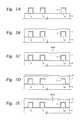
- FIG. 1A-1Eillustrates a three-layer deposition PECVD process for depositing a PECVD lining layer 2 of the oxidized organosilane or organosiloxane polymer as described in International Publication Number WO 99/41423.
- the lining layer 2acts as an isolation layer between a subsequent layer 7 and the underlying substrate surface 6 and metal lines 8 , 9 , 10 formed on the substrate surface.
- the layer 7is capped by a PECVD capping layer 12 of the oxidized organosilane or organosiloxane polymer.
- the PECVD processdeposits a multi-component dielectric layer, wherein an carbon containing silicon dioxide (SiO 2 ) is first deposited on the patterned metal layer having metal lines 8 , 9 , 10 formed on substrate 6 .
- SiO 2carbon containing silicon dioxide
- the PECVD lining layer 2is deposited by the plasma enhanced reaction of an organosilane or organosiloxane compound such as methylsilane, CH 3 SiH 3 , and an oxidizing gas such as N 2 O in the presence of an inert gas, such as argon, at a temperature of approximately ⁇ 20° C. to 40° C.
- an inert gassuch as argon
- the oxidized organosilane or organosiloxane layeris then cured.
- the deposited PECVD lining layer 2(at about 2000 ⁇ per minute) has improved barrier characteristics for the subsequent deposition of the layer 7 shown in FIG. 1B .
- the lining layer obtained from methylsilanehas sufficient C—H bonds to be hydrophobic, and is an excellent moisture barrier.
- a low K dielectric layer 7is then deposited on the liner layer 2 by the reaction of a silane compound and hydrogen peroxide (H 2 O 2 ) at a temperature below 200° C. at a pressure of about 0.2 to about 5 Torr during deposition of the layer 7 .
- the layer 7may be partially cured as shown in FIG. 1C to remove solvents such as water prior to deposition of a cap layer 12 as shown in FIG. 1D . Curing is performed by pumping down a reaction under an inert gas atmosphere under 10 Torr.
- an optional capping layer 12may be deposited on the low k dielectric layer 7 by the plasma enhanced reaction of an organosilane or organosiloxane compound and an oxidizing gas such as N 2 O.
- an oxidizing gassuch as N 2 O.
- the capping layer 12is also an oxidized organosilane or organosiloxane film that has good barrier properties and has a dielectric property of about 3.0. Both the liner layer 2 and the cap layer 12 have a dielectric constant greater than 3.0 and the high dielectric constant layers substantially detract from the benefit of the low k dielectric layer 7 .
- Lowering the parasitic capacitance between metal interconnects separated by dielectric materialcan be accomplished by either increasing the thickness of the dielectric material or by lowering the dielectric constant of the dielectric material. Increasing the thickness of the dielectric materials, however, does not address parasitic capacitance within the same metallized layer or plane. As a result, to reduce the parasitic capacitance between metal interconnects on the same or adjacent layers, one must change the material used between the metal lines or interconnects to a material having a lower dielectric constant than that of the materials currently used, i.e., k ⁇ 3.0.
- the present inventionprovides a method for depositing a nano-porous silicon oxide layer having a low dielectric constant.
- the nano-porous silicon oxide layeris produced by depositing a silicon/oxygen containing material that further contains thermally labile organic groups, and by controlled annealing of the deposited silicon/oxygen containing material to form microscopic gas pockets, or voids, that are uniformly dispersed in a silicon oxide layer.
- the relative volume of the microscopic gas pockets to the silicon oxide layeris controlled to preferably maintain a closed cell foam structure that provides low dielectric constants.
- the silicon/oxygen materialis deposited by plasma enhanced chemical vapor deposition of one or more compounds comprising at least one oxidizable silicon containing component and at least one non-silicon containing component having thermally labile groups.
- the labile groups in the reactive compound or mixturecontain sufficient oxygen to convert to gaseous products to evolve from the film and leave voids when the deposited silicon oxide layer is annealed.
- non-silicon containing components that form compounds with the silicon componentsare multiply unsaturated cycloalkene components including dioxinyl (—(—CH ⁇ CH—O—CH ⁇ CH—O—)—), furyl (—(—CH ⁇ CH—CH ⁇ CH—O—)—), fulvenyl (—(—CH ⁇ CH—CH ⁇ CH—C(CH 2 )—)—), or fluorinated carbon derivative groups thereof.
- Preferred compounds formed from these componentsinclude methylsilyl-1,4-dioxinyl ether or methylsiloxanyl furan. Formation of voids using 2,4,6-trisilaoxane and cyclo-1,3,5,7-tetrasilano-2,6-dioxy-4,8-dimethylene is enhanced by virtue of their non-planar ring structure.
- Such compoundsreact with an oxidizing gas to form a silicon/oxygen containing material that retains many of the labile organic groups at temperatures below about 50° C.
- the amount of labile groupscan be increased by mixing the reactive compounds with non-silicon containing components that comprise one or more labile groups, such as vinyl-1,4-dioxinyl ether, vinyl furyl ether, vinyl-1,4-dioxin, vinyl furan, methyl furoate, furyl formate, furyl acetate, furaldehyde, difuryl ketone, difuryl ether, difurfuryl ether, furan, 1,4-dioxin, fluorinated derivatives thereof, and combinations thereof.
- labile groupssuch as vinyl-1,4-dioxinyl ether, vinyl furyl ether, vinyl-1,4-dioxin, vinyl furan, methyl furoate, furyl formate, furyl acetate, furaldehyde, difuryl
- the non-silicon containing componentscan alternatively be mixed with the reactive silicon containing materials that do not contain thermally labile organic groups, such as methylsilane, dimethylsilane, 1,1,3,3-tetramethyldisiloxane, 1,1,5,5-tetramethyltrisiloxane, disilanomethane, and fluorinated carbon derivatives thereof.
- thermally labile organic groupssuch as methylsilane, dimethylsilane, 1,1,3,3-tetramethyldisiloxane, 1,1,5,5-tetramethyltrisiloxane, disilanomethane, and fluorinated carbon derivatives thereof.
- the silicon/oxygen containing materialis preferably deposited by striking a plasma at an RF power level from 10-250 W in an oxidizing gas selected from the group consisting of N 2 O, O 2 , O 3 , CO 2 , and combinations thereof.
- the deposited silicon/oxygen containing materialis then annealed at a gradually increasing temperature profile to convert the labile organic groups to dispersed gas pockets in a nano-porous silicon oxide layer having a low dielectric constant attributed to a preferably closed cell foam structure. Annealing preferably increases the temperature of the deposited material to about 350° C. to about 400° C.
- the nano-porous silicon oxide layer of the present inventionis deposited on a PECVD silicon oxide, silicon nitride, silicon oxynitride, or hydrogenated silicon carbide barrier layer that was deposited on a patterned metal layer by plasma assisted reaction of one or more reactive silicon containing compounds.
- the nano-porous silicon oxide layeris then deposited in the same chamber or in an adjacent cluster tool processing chamber. After annealing as described above, the nano-porous silicon oxide layer is capped in the same chamber or in an adjacent cluster tool processing chamber with PECVD silicon oxide, silicon nitride, silicon oxynitride, or hydrogenated silicon carbide.
- the liner and cap layersserve as barriers which protect the nano-porous silicon oxide layer.
- FIG. 1A-1Eare schematic diagrams of dielectric layers deposited on a substrate by the processes known in the art
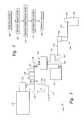
- FIG. 2is a cross-sectional diagram of an exemplary CVD reactor configured for use according to the present invention
- FIG. 3is a schematic diagram of a remote microwave chamber for dissociation of process gases prior to entering the reactor of FIG. 2 ;
- FIG. 4is a flowchart of a process control computer program product used in conjunction with the exemplary CVD reactor of FIG. 2 ;
- FIG. 5is a flow chart illustrating steps undertaken in depositing liner and cap layers in a deposition process according to one embodiment of the present invention
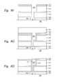
- FIG. 6A-6Eis a schematic diagram of the layers deposited on a substrate by the process of FIG. 5 ;
- FIG. 7is a cross sectional view showing a dual damascene structure comprising the silicon oxide layers of the present invention.
- FIGS. 8A-8Hare cross sectional views showing one embodiment of a dual damascene deposition sequence of the present invention.
- the present inventionprovides a method for depositing a nano-porous silicon oxide layer having a low dielectric constant.
- the nano-porous silicon oxide layeris produced by plasma enhanced (PECVD) or microwave enhanced chemical vapor deposition of a silicon/oxygen containing material that optionally contains thermally labile organic groups, and by controlled annealing of the deposited silicon/oxygen containing material to form microscopic gas pockets that are uniformly dispersed in a silicon oxide layer.
- the relative volume of the microscopic gas pockets to the silicon oxide layeris controlled to preferably maintain a closed cell foam structure that provides low dielectric constants after annealing.
- the nano-porous silicon oxide layerswill have dielectric constants less than about 2.5, preferably less than about 2.0.
- the silicon/oxygen materialis chemical vapor deposited by reacting an oxidizable silicon containing compound or mixture comprising an oxidizable silicon component and an unsaturated non-silicon bearing component having thermally labile groups with an oxidizing gas.
- the oxidizing gasesare oxygen (O 2 ) or oxygen containing compounds such as nitrous oxide (N 2 O), ozone (O 3 ), and carbon dioxide (CO 2 ), preferably N 2 O or O 2 .
- Oxygen and oxygen containing compoundsare preferably dissociated to increase reactivity when necessary to achieve a desired carbon content in the deposited film.
- RF powercan be coupled to the deposition chamber to increase dissociation of the oxidizing compounds.
- the oxidizing compoundsmay also be dissociated in a microwave chamber prior to entering the deposition chamber to reduce excessive dissociation of the silicon containing compounds.
- Deposition of the silicon oxide layercan be continuous or discontinuous. Although deposition preferably occurs in a single deposition chamber, the layer can be deposited sequentially in two or more deposition chambers.
- RF powercan be cycled or pulsed to reduce heating of the substrate and promote greater porosity in the deposited film.
- the oxidizable silicon component of the oxidizable silicon containing compound or mixturecomprises organosilane or organosiloxane compounds which generally include the structure:
- each Siis bonded to at least one hydrogen atom and may be bonded to one or two carbon atoms, and C is included in an organo group, preferably alkyl or alkenyl groups such as —CH 3 , —CH 2 —CH 3 , —CH 2 —, or —CH 2 —CH 2 —, or fluorinated carbon derivatives thereof.
- an organosilane or organosiloxane compoundincludes two or more Si atoms
- each Siis separated from another Si by —O—, —C—, or —C—C—
- each bridging Cis included in an organo group, preferably alkyl or alkenyl groups such as —CH 2 —, —CH 2 —CH 2 —, —CH(CH 3 )—, —C(CH 3 ) 2 —, or fluorinated carbon derivatives thereof.
- the preferred organosilane and organosiloxane compoundsare gases or liquids near room temperature and can be volatilized above about 10 Torr.
- Suitable silicon containing compoundsinclude:
- the hydrocarbon groups in the organosilanes and organosiloxanemay be partially or fully fluorinated to convert C—H bonds to C—F bonds.
- Many of the preferred organosilane and organosiloxane compoundsare commercially available.
- a combination of two or more of the organosilanes or organosiloxanescan be employed to provide a blend of desired properties such as dielectric constant, oxide content, hydrophobicity, film stress, and plasma etching characteristics.
- the organosilane or organosiloxane compoundare functional groups possessing both a silicon oxygen bond and a silicon-hydrogen bond.
- Preferred functional groups having the bonding requirementsinclude:
- the unsaturated non-silicon bearing component having thermally labile groupshas the property of reacting with an plasma-sustained oxidizing environment to form thermally labile molecules that deposit, and which, when subsequently exposed to elevated temperatures, thermally decompose to form volatile species with low boiling points. Decomposition and evolution of the thermally labile group's volatile species from the deposited film will leave voids in the structure, reducing the structure's density. Selectively removing embedded chemically reacted solid material within the deposited film by a thermal process results in low density films which have low dielectric constants.
- the thermally labile organic groupscontain sufficient oxygen to form gaseous products when the silicon oxide layer is annealed.
- thermally labile groupsare non-silicon containing multiply unsaturated cycloalkanes (having two or more carbon-carbon double bonds), including heterocyclodialkenes, with oxygen or nitrogen incorporated within the molecular structure, and which generally tend to perform favorably in plasma environments.
- Preferred labile groupsinclude:
- Oxidizable silicon containing compoundscomprising the oxidizable silicon component and the thermally labile groups include:
- the compoundsare liquid at room temperature and can be volatilized near a pressure of 10 Torr or above.
- Such compoundsreact with an oxidizing gas to form a gel-like silicon/oxygen containing material that retains many of the labile organic groups at temperatures below about 50° C.
- the amount of labile organic groups retained in the deposited silicon/oxygen containing materialcan be increased by mixing the reactive compounds with non-silicon containing components that comprise one or more labile organic groups.
- the labile organic groupsinclude the dioxan, furan, and fulvene derivative chemicals described for the silicon containing reactive compounds and other oxygen containing organic groups.
- the labile organic groupsare preferably the silicon containing and non-silicon containing components incorporated in the same molecule, but with the methylsilyl or methylsiloxanyl groups replaced with vinyl groups, or with the methylsiloxanyl groups replaced with ester groups, or with the methylsiloxanyl groups replaced with other non-silicon containing organic groups, in addition to those chemicals without the methylsiloxanyl groups, such as 1,4-dioxin and furan.
- Preferred non-silicon containing multiply unsaturated cycloalkanesinclude:
- the non-silicon containing componentscan alternatively be mixed with the reactive silicon containing materials that do not contain labile organic groups, such as:
- thermally-labile-imparting and non-thermally-labile-imparting compoundscan be co-deposited to tailor film properties.
- a preferred embodiment of the co-deposition compoundsinclude a thermally-labile-imparting compound selected from either methylsilyl-1,4-dioxinyl ether or 2-methylsiloxanyl furan and a non-thermally-labile-imparting compound selected from either 2,4,6-trisilaoxane (2,4,6-trisilatetrahydropyran) or cyclo-1,3,5,7-tetrasilano-2,6-dioxy-4,8-dimethylene.
- the co-deposited heteroalicyclic non-thermally-labile imparting molecules which can be used advantageouslyare non-planar cyclic molecules with insignificant ring strain and which deposit in random orientations.
- the dual bonding of the silyl functional groups to the methylene groupscan provide improved thermal stability and better mechanical properties of the resultant film.
- the non-planar moleculecan provide a relatively reduced stack density within the deposited film, thereby producing low dielectric films.
- the filmis preferably annealed at a gradually increasing temperature to convert the labile organic groups to dispersed gas pockets in a nano-porous silicon oxide layer having a low dielectric constant attributed to a preferably closed cell foam structure.
- the nano-porous silicon oxide layer of the present inventionis deposited on a PECVD silicon oxide, silicon nitride, silicon oxynitride, or hydrogenated silicon carbide (e.g., BLOkTM layer material available from Applied Materials Inc., of Santa Clara, Calif.) barrier layer that was deposited on a patterned metal layer by plasma assisted reaction of one or more reactive silicon containing compounds.
- the nano-porous silicon oxide layeris then deposited in the same multichamber clustered CVD system while applying RF power or remote microwave power, and is subsequently heated using an increasing temperature profile, optionally to between about 350° C. to about 400° C.
- the nano-porous silicon oxide layeris optionally capped in the same chamber or in an adjacent cluster tool processing chamber used to deposit the barrier layer, for example with a hydrogenated silicon carbide (BLOkTM).
- BLOkTMhydrogenated silicon carbide
- the liner and cap layersserve as barriers which protect the nano-porous silicon oxide layer.
- the chemical usedis preferably selected from a group consisting of hexamethyldisilazane, trimethylsilyldiethylamine, phenyldimethylsilyldimethylamine, trimethoxysilyldimethylamine, tris(trifluoromethyl)silyldimethylamine, bis(trimethyl-silyl)hydrazine, 1-phenyldimethylsilyl-2-methyl-hydrazine, 1-trimethoxysilyl-2-methyl-hydrazine, 1-tris(trifluoromethylsilyl)-2-methyl-hydrazine, trimethylchlorosilane, trimethylbromosilane, trimethylsilane, or combinations thereof.
- the liner and cap layerscan be deposited by plasma assisted chemical vapor deposition (CVD) of silicon oxide, silicon nitride, silicon oxynitride, or hydrogenated silicon carbide (BLOkTM).
- CVDplasma assisted chemical vapor deposition
- FIG. 2is a vertical, cross-section view of a parallel plate chemical vapor deposition reactor 110 having a high vacuum region 115 .
- Reactor 110contains a gas distribution manifold 111 for dispersing process gases through perforated holes in the manifold to a substrate or substrate (not shown) that rests on a substrate support plate or susceptor 112 which is raised or lowered by a lift motor 114 .
- a liquid injection system(not shown), such as typically used for liquid injection of TEOS, may also be provided for injecting a liquid reactant.
- Preferred liquid injection systemsinclude the AMAT Gas Precision Liquid Injection System (GPLIS) and the AMAT Extended Precision Liquid Injection System (EPLIS), both available from Applied Materials, Inc.
- GPLISAMAT Gas Precision Liquid Injection System
- EPLISAMAT Extended Precision Liquid Injection System
- the reactor 110includes heating of the process gases and substrate, such as by resistive heating coils (not shown) or external lamps (not shown).
- susceptor 112is mounted on a support stem 113 so that susceptor 112 (and the substrate supported on the upper surface of susceptor 112 ) can be controllably moved between a lower loading/off-loading position and an upper processing position which is closely adjacent to manifold 111 .
- susceptor 112 and the substrateWhen susceptor 112 and the substrate are in processing position 114 , they are surrounded by an insulator 117 and process gases exhaust into a manifold 124 . During processing, gases inlet to manifold 111 are uniformly distributed radially across the surface of the substrate.
- a vacuum pump 132 having a throttle valvecontrols the exhaust rate of gases from the chamber.
- deposition and carrier gasesare input through gas lines 118 into a mixing system 119 where they are combined and then sent to manifold 111 .
- An optional microwave system 150shown in FIG. 3 ) having a applicator tube 120 may be located on the input gas line for the oxidizing gas to provide additional energy that dissociates only the oxidizing gas prior to entry to the reactor 110 .
- the microwave applicatorprovides a power from between about 0 and about 6000 W.
- the process gases supply lines 18 for each of the process gasesinclude (i) safety shut-off valves (not shown) that can be used to automatically or manually shut off the flow of process gas into the chamber, and (ii) mass flow controllers (also not shown) that measure the flow of gas through the gas supply lines.
- safety shut-off valvesnot shown
- mass flow controllersalso not shown
- the deposition process performed in reactor 110can be either a non-plasma process on a cooled substrate pedestal or a plasma enhanced process.
- a controlled plasmais typically formed adjacent to the substrate by RF energy applied to distribution manifold 111 from RF power supply 125 (with susceptor 112 grounded).
- RF powercan be provided to the susceptor 112 or RF power can be provided to different components at different frequencies.
- RF power supply 125can supply either single or mixed frequency RF power to enhance the decomposition of reactive species introduced into the high vacuum region 115 .
- a mixed frequency RF power supplytypically supplies power at a high RF frequency (RF 1 ) of about 13.56 MHz to the distribution manifold 111 and at a low RF frequency (RF 2 ) of about 360 KHz to the susceptor 112 .
- the silicon oxide layers of the present inventionare most preferably produced using low levels or pulsed levels of high frequency RF power.
- Pulsed RF powerpreferably provides 13.56 MHz RF power at about 20 to about 200 W during about 10% to about 30% of the duty cycle.
- Non-pulsed RF powerpreferably provides 13.56 MHz RF power at about 10 to about 150 W as described in more detail below.
- Low power depositionpreferably occurs at a temperature range from about ⁇ 20 to about 40° C. At the preferred temperature range, the deposited film is partially polymerized during deposition and polymerization is completed during subsequent curing of the film.
- an optional microwave chambercan be used to input from about 0 to about 3000 W of microwave power to the oxidizing gas prior to entering the deposition chamber. Separate addition of microwave power would avoid excessive dissociation of the silicon compounds prior to reaction with the oxidizing gas.
- a gas distribution plate having separate passages for the silicon compound and the oxidizing gasis preferred when microwave power is added to the oxidizing gas.
- any or all of the chamber lining, gas inlet manifold faceplate, support stem 113 , and various other reactor hardwareis made out of material such as aluminum or anodized aluminum.
- An example of such a CVD reactoris described in U.S. Pat. No. 5,000,113, entitled “Thermal CVD/PECVD Reactor and Use for Thermal Chemical Vapor Deposition of Silicon Dioxide and In-situ Multi-step Planarized Process,” issued to Wang et al. and assigned to Applied Materials, Inc., the assignee of the present invention.
- the lift motor 114raises and lowers susceptor 112 between a processing position and a lower, substrate-loading position.
- the motor, the gas mixing system 119 , and the RF power supply 125are controlled by a system controller 134 over control lines 136 .
- the reactorincludes analog assemblies, such as mass flow controllers (MFCs) and standard or pulsed RF generators, that are controlled by the system controller 134 which executes system control software stored in a memory 210 , which in the preferred embodiment is a hard disk drive.
- MFCsmass flow controllers
- RF generatorsstandard or pulsed RF generators
- the system controller 134controls all of the activities of the CVD reactor and a preferred embodiment of the controller 134 includes a hard disk drive, a floppy disk drive, and a card rack.
- the card rackcontains a single board computer (SBC), analog and digital input/output boards, interface boards and stepper motor controller boards.
- SBCsingle board computer
- the system controllerconforms to the Versa Modular Europeans (VME) standard which defines board, card cage, and connector dimensions and types.
- VMEVersa Modular Europeans
- the VME standardalso defines the bus structure having a 16-bit data bus and 24-bit address bus.
- FIG. 3is a simplified diagram of a remote microwave system 150 for dissociating process gases such as water prior to entering the DLK reactor 110 , in accordance with an embodiment of the present invention.
- Remote microwave system 150includes an applicator tube 120 , a plasma ignition system including an ultraviolet (UV) lamp 154 and a UV power supply 155 , a microwave waveguide system that includes various lengths of straight and curved waveguide sections 156 , waveguide coupling 158 , which may be connected together at joints 157 , an output waveguide section 160 , and a magnetron 168 .
- the waveguide section 156may further have an arm support 162 formed therein for attachment to an pivoting arm 164 mounted on a arm base 166 .
- the pivoting armcomprises arm pieces 165 coupled to arm joints 163 that provide vertical separation of the arm pieces and allow rotational movement of the arm 164 around the arm joints 163 .
- the arm joints 163are vertically disposed cylinders coupled to one arm piece 165 at the bottom of the arm joint 163 and coupled to a second arm piece 165 at the top of the arm joint 165 .
- the attachment of the arm pieces 165 at the ends of the arm joint 163allow for vertical separation of the arm pieces and flexibility of position the arm 164 , and thus the microwave system 150 , during operation and maintenance of the processing reactor 110 .
- Magnetron 168is a typical magnetron source capable of operating between about 0-3000 Watts for continuous wave (CW) or pulsed output of microwaves of about 2.45 Gigahertz (GHz) frequency. Of course, other magnetrons may be utilized as well. Circulator (not shown) allows only forward microwave transmission from magnetron 168 toward applicator tube 120 .
- Tuning system 170which may use stub tuners or other tuning elements, provides the microwave system 150 with the ability to match the load at waveguide section 160 to the characteristic impedance of the waveguides. Tuning system 170 may provide fixed tuning, manual tuning, or automated tuning, according to specific embodiments. In the specific embodiment, the waveguide sections have rectangular cross-sections, but other types of waveguide also may be used.
- Applicator tube 120is a circular (or other cross-section) tube made of a composite or ceramic material, preferably alumina, or other material resistant to etching by radicals.
- applicator tube 120has a length of about 18-24 inches and a cross-sectional diameter of about 3-4 inches.
- Applicator tube 120is disposed through a waveguide section 160 , which is open at one end for transmitting microwaves and is terminated at the other end with a metal wall. Microwaves are transmitted through the open end of waveguide section 160 to gases inside applicator tube 120 , which is transparent to microwaves.
- other materialssuch as sapphire also may be used for the interior of applicator tube 120 .
- applicator tube 120may have a metal exterior and an interior made of a composite or ceramic material wherein microwaves in waveguide section 160 enter a window through the exterior of applicator tube 120 to the exposed interior of tube 120 to energize the gases.
- FIG. 4shows a block diagram of a processing system, or reactor 110 , such as that depicted in FIG. 2 , having such a system controller 134 that can be employed in such a capacity.
- the system controller 134includes a programmable central processing unit (CPU) 220 that is operable with a memory 210 , a mass storage device 215 , an input control unit 245 , and a display unit 255 .
- CPUprogrammable central processing unit
- the system controllerfurther includes well-known support circuits 214 such as power supplies, clocks 225 , cache 235 , input/output (I/O) circuits 240 and the like, coupled to the various components of the DLK process reactor 110 to facilitate control of the deposition process.
- the controller 134also includes hardware for monitoring substrate processing through sensors (not shown) in the chamber 110 . Such sensors measure system parameters such as substrate temperature, chamber atmosphere pressure and the like. All of the above elements are coupled to a control system bus 230 .
- the CPU 220may be one of any form of general purpose computer processor that can be used in an industrial setting for controlling various chambers and subprocessors.
- the memory 210is coupled to the CPU 220 , and is accessible to the system bus 230 .
- the memory 210 , or computer-readable medium 215may be one or more of readily available memory such as random access memory (RAM), read only memory (ROM), floppy disk drive, hard disk, or any other form of digital storage, local or remote.
- the support circuits 214are coupled to the CPU 220 for supporting the processor in a conventional manner.
- the deposition processis generally stored in the memory 210 , typically as a software routine.
- the software routinemay also be stored and/or executed by a second CPU (not shown) that is remotely located from the hardware being controlled by the CPU 220 .
- the memory 210contains instructions that the CPU 220 executes to facilitate the performance of the processing system 10 .
- the instructions in the memory 210are in the form of program code such as a program 200 that implements the method of the present invention.
- the program codemay conform to any one of a number of different programming languages. For example, the program code can be written in C, C++, BASIC, Pascal, or a number of other languages.
- the mass storage device 215stores data and instructions are retrieves data and program code instructions from a processor readable storage medium, such as a magnetic disk or magnetic tape.
- a processor readable storage mediumsuch as a magnetic disk or magnetic tape.
- the mass storage device 215can be a hard disk drive, floppy disk drive, tape drive, or optical disk drive.
- the mass storage device 215stores and retrieves the instructions in response to directions that it receives from the CPU 220 .
- Data and program code instructions that are stored and retrieved by the mass storage device 215are employed by the processor unit 220 for operating the processing system.
- the data and program code instructionsare first retrieved by the mass storage device 215 from a medium and then transferred to the memory 210 for use by the CPU 220 .
- the input control unit 245couples a data input device, such as a keyboard, mouse, or light pen, to the processor unit 220 via the system bus 230 to provide for the receipt of a chamber operator's inputs.
- the display unit 255provides information to a chamber operator in the form of graphical displays and alphanumeric characters under control of the CPU 220 .
- the control system bus 230provides for the transfer of data and control signals between all of the devices that are coupled to the control system bus 230 .
- the control system busis displayed as a single bus that directly connects the devices in the CPU 220
- the control system bus 230can also be a collection of busses.
- the display unit 255 , input control unit 245 (with input device), and mass storage device 215can be coupled to an input-output peripheral bus, while the CPU 220 and memory 210 are coupled to a local processor bus.
- the local processor bus and input-output peripheral busare coupled together to form the control system bus 230 .
- the system controller 134is coupled to the elements of the processing system 10 , employed in dielectric deposition processes in accordance with the present invention via the system bus 230 and the I/O circuits 240 .
- the I/O circuits 240receive instructions from the program 200 stored in memory 210 via the CPU 220 and system bus 230 .
- the program 200provides program subroutines that enable the I/O circuits 240 to provide for substrate positioning control 250 , process gas control 260 , pressure control 270 , heater control 280 , and plasma/microwave control 290 , of the reactor 110 .
- the CPU 220forms a general purpose computer that becomes a specific purpose computer when executing programs such as the program 200 of the embodiment of the method of the present invention depicted in the flow diagram of FIG. 4 .
- programssuch as the program 200 of the embodiment of the method of the present invention depicted in the flow diagram of FIG. 4 .
- ASICapplication specific integrated circuit
- CVD system descriptionis mainly for illustrative purposes, and other plasma CVD equipment such as electrode cyclotron resonance (ECR) plasma CVD devices, induction-coupled RF high density plasma CVD devices, or the like may be employed. Additionally, variations of the above described system such as variations in susceptor design, heater design, location of RF power connections and others are possible. For example, the substrate could be supported and heated by a resistively heated susceptor.
- ECRelectrode cyclotron resonance
- the pretreatment and method for forming a pretreated layer of the present inventionis not limited to any specific apparatus or to any specific plasma excitation method.
- the nano-porous silicon oxide layer of the present inventioncan be deposited in a three-layer process as shown in FIG. 5 using the PECVD or microwave chamber of FIG. 2 .
- a substrateis positioned 300 in the reactor 110 and a barrier layer is deposited 305 by a PECVD process from a plasma comprising a reactive silicon containing compound.
- the deposition step 305can include a capacitively coupled plasma or both an inductively and a capacitively coupled plasma in the process chamber 15 according to methods known in the art.
- An inert gassuch as helium is commonly used in the PECVD deposition to assist in plasma generation.
- a nano-porous layer of the present inventionis then deposited 310 on the liner layer by depositing a silicon/oxygen containing material that further contains labile organic groups, and by controlled annealing of the deposited silicon/oxygen containing material to form microscopic gas pockets that are uniformly dispersed in the layer.
- a cap layeris then deposited 315 on the layer, preferably using a similar process as employed for depositing the lining layer.
- the substrateis then removed 320 from the reactor 110 .
- the three-layer processprovides a PECVD lining layer 400 .
- the lining layer 400acts as an isolation layer between the subsequent nano-porous layer 402 and the underlying substrate surface 404 and metal lines 406 , 408 , 410 formed on the substrate surface.
- the nano-porous layer 402is capped by a PECVD capping layer 412 of the silicon containing compound. This process is implemented and controlled using a computer program stored in the memory 220 of a computer controller 134 for a CVD reactor 110 .
- the PECVD lining layer 400is deposited in the reactor 110 by introducing a reactive silicon containing compound and an oxidizing gas.
- the process gasesreact in a plasma enhanced environment to form a conformal silicon oxide layer 400 on the substrate surface 404 and metal lines 406 , 408 , 410 .
- the nano-porous layer 402is deposited from a processing gas consisting of silicon and labile containing compounds and an oxidizing gas.
- the process gas flowsrange from about 20 to about 1000 sccm for the silicon and labile containing compounds, and about 5 to about 4000 sccm of the oxidizing gas.
- the preferred gas flowsrange from about 50 to about 500 sccm for the silicon and labile containing compounds and a flow rate of about 5 to about 2000 sccm of the oxidizing gas. These flow rates are given for a chamber having a volume of approximately 5.5 to 6.5 liters.
- reactor 110is maintained at a pressure of about 0.2 to about 5 Torr during deposition of the nano-porous layer 402 .
- the nano-porous layer 402is cured as shown in FIG. 6C to remove volatile constituents prior to deposition of a cap layer 412 as shown in FIG. 6D . Curing can be performed in the reactor 110 under an inert gas atmosphere while heating the substrate to progressively higher temperatures.
- the nano-porous layer 402is preferably annealed at a gradually increasing temperature to retain gaseous products as dispersed microscopic bubbles, and/or to convert the optional labile organic groups to dispersed microscopic gas bubbles that are retained in the cured silicon oxide film as voids in a preferably closed cell structure.
- a preferred anneal processcomprises a heating time period of about 5 minutes, including gradually raising the temperature by about 50° C./min. to a final temperature of between about 350° C. to about 400° C.
- Dispersion of the gas bubblescan be controlled by varying the temperature/time profile and by controlling the concentration of labile organic groups in the deposited film.
- the reactor 110deposits a capping layer 412 , preferably of the same material and by the same methods as used for the deposition of the PECVD liner layer 400 .
- a capping layer 412preferably of the same material and by the same methods as used for the deposition of the PECVD liner layer 400 .
- the deposited layersare further annealed in a furnace or another chamber at a temperature from about 200° C. to about 450° C. to drive off remaining volatile products such as water.
- processing conditionswill vary according to the desired characteristics of the deposited films.
- FIG. 7A preferred dual damascene structure 500 fabricated in accordance with the invention is shown in FIG. 7 , and the method of making the structure is sequentially depicted schematically in FIGS. 8A-8H , which are cross sectional views of a substrate having the steps of the invention formed thereon.
- a dual damascene structure 500 which includes a nano-porous intermetal dielectric layer 510is shown in FIG. 7 .
- the intermetal dielectric layers 510 and 514 deposited according to the inventionhave extremely low dielectric constants of less than 3, and are often referred to as extreme low k, or ELk, dielectric layers.
- a first dielectric layer 510preferably consisting of the nano-porous silicon oxide layer of the present invention is deposited on a substrate 502 .
- the substratecomprising patterned conducting lines 506 formed in a contact level substrate material 504 , with a first (or substrate) etch stop 508 of silicon oxide, silicon nitride, silicon oxynitride, or amorphous hydrogenated silicon carbide (BLOkTM), preferably silicon nitride, deposited thereon.
- a silicon oxide, silicon nitride, silicon oxynitride, or hydrogenated silicon carbide (BLOkTM) second etch stop 512is deposited on the first dielectric layer 510 .
- a second dielectric layer 514preferably consisting of the nano-porous silicon oxide layer of the present invention is deposited on the second etch stop 512 , with a third etch stop 516 deposited on the second dielectric layer 514 .
- the deposited layersare etched to form a via 520 , which is subsequently filled with a conducting metal 524 , preferably copper, over a barrier layer 522 conformally deposited within the via 520 .
- the structureis then planarized and a capping layer 518 comprising silicon nitride, silicon oxide, silicon oxynitride, or hydrogenated silicon carbide, preferably comprising silicon nitride, is deposited thereon.
- the capping layer 518also serves as the substrate etch stop and corresponds to the first etch stop 508 for subsequent dual damascene multilevel interconnects.
- a first (or substrate) etch stop 508 of silicon oxide, silicon nitride, silicon oxynitride, or amorphous hydrogenated silicon carbide, preferably silicon nitrideis deposited to a thickness of about 1000 ⁇ on the substrate 502 .
- the substrate 502comprises patterned conducting interconnects or lines 506 formed in a contact level substrate material 504 .
- a first nano-porous dielectric layer 510is deposited according to the invention on the first etch stop 508 .
- the first dielectric layer 510has a thickness of about 5,000 ⁇ to about 10,000 ⁇ , depending on the size of the structure to be fabricated, but has a preferable thickness of about 5,000 ⁇ .
- the first dielectric layer 510and is then annealed at a temperature of about 350° C. to about 400° C. to remove volatile contaminants from the layer 510 .
- a second etch stop 512such as silicon oxynitride, is deposited on the dielectric layer 510 to a thickness of about 500 ⁇ .
- a second nano-porous dielectric layer 514is then deposited a thickness of about 5,000 ⁇ to about 10,000 ⁇ , preferably about 5,000 ⁇ , according to the invention on the first etch stop 508 , and is then annealed at a temperature of about 350° C. to about 400° C.
- An anti-reflective coating (ARC) 519 and a trench photomask comprising a photoresist layer 521are then respectfully deposited over the silicon oxide layer 517 .
- the photoresist layer 521is then patterned by conventional photolithography means known in the art.
- the silicon oxide layer 517is then etched by conventional means known in the art, preferably by an etch process using fluorocarbon chemistry, to expose the third etch 516 as shown in FIG. 8B .
- the initial etch of the silicon oxide layer 517establishes the opening width, or trench width, of the dual damascene structure 500 .
- the opening width formed in the silicon oxide layer 517defines the horizontal interconnect of the dual damascene structure 500 formed above the second etch stop 514 .
- the remaining photoresist 521is then ashed, or dry removed, for preparation of the via etch.
- a second anti-reflective coating 519 and a photoresist layer 521are then respectfully deposited over the thin silicon oxide layer 517 , and then patterned by photolithography to expose the third etch layer 516 by the via width as shown in FIG. 8C .
- the third etch stop 516 and second dielectric layer 514are trenched etched to expose the second etch stop 512 .
- the via 520is then formed by via etching the second dielectric layer 514 to the second etch stop 512 using anisotropic etching techniques to define the metallization structure (i.e., the interconnect and contact/via) at the width established by the silicon oxide layer 517 ; and etching the first dielectric layer 510 to the first etch stop 508 at the via width established during the etching of the third etch stop 516 , second dielectric layer 514 , and the second etch stop 512 as shown in FIG. 8E .
- FIG. 8Fshows the etching of the first etch stop 508 protecting the substrate 502 , exposing the underlying patterned metal lines 506 in the contact level substrate material 504 .
- the patterned metal lines 506preferably comprise a conducting metal such as copper.
- the dual damascene structure 500is then precleaned by conventional means known in the art prior to subsequent layer deposition.
- the metallization structureis then formed with a conductive material such as aluminum, copper, tungsten or combinations thereof.
- a conductive materialsuch as aluminum, copper, tungsten or combinations thereof.
- the trendis to use copper to form the smaller features due to the low resistivity of copper (1.7 mW-cm compared to 3.1 mW-cm for aluminum).
- a suitable barrier layer 522such as tantalum nitride is first deposited conformally in the metallization pattern 520 to prevent copper migration into the surrounding silicon and/or dielectric material.
- a layer of copper 524is deposited using either chemical vapor deposition, physical vapor deposition, electroplating, preferably by electroplating, to form the conductive structure.
- the surfaceis planarized using chemical mechanical polishing and capped with a capping layer 518 , preferably comprising silicon nitride and having a thickness of about 1000 ⁇ , as shown in FIG. 8H .
- the metalPrior to planarizing the surface, the metal may be annealed in a hydrogen atmosphere to recrystallize the copper fill and to remove voids that may have formed in the structure 500 .
- a copper seed layermay be deposited prior to the copper layer 524 when the copper layer 524 is deposited by an electroplating process. The dual damascene formation process may then be repeated to deposit further interconnection levels, of which modern microprocessor integrated circuits have 5 or 6 interconnection levels.
- the following examplesdemonstrate deposition of a nano-porous silicon oxide based film having dispersed microscopic gas voids. This example is undertaken using a chemical vapor deposition chamber, and in particular, a CENTURA “DLK” system fabricated and sold by Applied Materials, Inc., Santa Clara, Calif.
- a nano-porous silicon oxide based filmis deposited at a chamber pressure of 1.0 Torr and temperature of 30° C. from reactive gases which are vaporized and flown into the reactor as follows:
- nitrous oxideN 2 O
- the nitrous oxidePrior to entering the chamber, the nitrous oxide is dissociated in a microwave applicator that provides 2000 W of microwave energy.
- the substrateis positioned 600 mil from the gas distribution showerhead and the reactive gases are introduced for 2 minutes.
- the substrateis then heated over a time period of 5 minutes, raising the temperature of the substrate by 50° C./min to a temperature of 400° C. to cure and anneal the nano-porous silicon oxide based film.
- a nano-porous silicon oxide based filmis deposited at a chamber pressure of 1.0 Torr and temperature of 30° C. from reactive gases which are vaporized and flown into the reactor as follows:
- nitrous oxidePrior to entering the chamber, the nitrous oxide is dissociated in a microwave applicator that provides 2000 W of microwave energy.
- the substrateis positioned 600 mil from the gas distribution showerhead and the reactive gases are introduced for 2 minutes.
- the substrateis then heated over a time period of 5 minutes, raising the temperature of the substrate by 50° C./min to a temperature of 400° C. to cure and anneal the nano-porous silicon oxide based film.
- a nano-porous silicon oxide based filmis deposited at a chamber pressure of 1.0 Torr and temperature of 0° C. from reactive gases which are vaporized and flown into the reactor as follows:
- methylsilyl-2-furyl etherat 100 sccm cyclo-1,3,5,7-tetrasilylene-2,6-dioxy-4,8 dimethylene, at 50 sccm Nitrous Oxide (N 2 O), at 1000 sccm.
- the nitrous oxidePrior to entering the chamber, the nitrous oxide is dissociated in a microwave applicator that provides 2000 W of microwave energy.
- the substrateis positioned 600 mil from the gas distribution showerhead and the reactive gases are introduced for 2 minutes.
- the substrateis then heated over a time period of 5 minutes, raising the temperature of the substrate by 50° C./min to a temperature of 400° C. to cure and anneal the nano-porous silicon oxide based film.
Landscapes
- Engineering & Computer Science (AREA)
- Chemical & Material Sciences (AREA)
- Physics & Mathematics (AREA)
- Condensed Matter Physics & Semiconductors (AREA)
- General Physics & Mathematics (AREA)
- Manufacturing & Machinery (AREA)
- Computer Hardware Design (AREA)
- Microelectronics & Electronic Packaging (AREA)
- Power Engineering (AREA)
- Chemical Kinetics & Catalysis (AREA)
- General Chemical & Material Sciences (AREA)
- Materials Engineering (AREA)
- Mechanical Engineering (AREA)
- Metallurgy (AREA)
- Organic Chemistry (AREA)
- Inorganic Chemistry (AREA)
- Plasma & Fusion (AREA)
- Formation Of Insulating Films (AREA)
- Internal Circuitry In Semiconductor Integrated Circuit Devices (AREA)
- Chemical Vapour Deposition (AREA)
Abstract
Description
This application is a continuation application of co-pending patent application Ser. No. 11/424,790, which application is a divisional of U.S. patent application Ser. No. 10/404,830, filed Apr. 1, 2003, now issued as U.S. Pat. No. 7,205,224, which application is a continuation of U.S. patent application Ser. No. 09/484,689, filed Jan. 18, 2000, now issued as U.S. Pat. No. 6,541,367, all of which are incorporated herein by reference.
1. Field of the Invention
The present invention relates to the fabrication of integrated circuits. More particularly, the invention relates to a process for depositing dielectric layers on a substrate.
2. Background of the Invention
One of the primary steps in the fabrication of modern semiconductor devices is the formation of metal and dielectric films on a substrate by chemical reaction of gases. Such deposition processes are referred to as chemical vapor deposition or CVD. Conventional thermal CVD processes supply reactive gases to the substrate surface where heat-induced chemical reactions take place to produce a desired film. The high temperatures at which some thermal CVD processes operate can damage device structures having layers previously formed on the substrate. A preferred method of depositing metal and dielectric films at relatively low temperatures is plasma-enhanced CVD (PECVD) techniques such as described in U.S. Pat. No. 5,362,526, entitled “Plasma-Enhanced CVD Process Using TEOS for Depositing Silicon Oxide”, which is incorporated by reference herein. Plasma-enhanced CVD techniques promote excitation and/or disassociation of the reactant gases by the application of radio frequency (RF) energy to a reaction zone near the substrate surface, thereby creating a plasma of highly reactive species. The high reactivity of the released species reduces the energy required for a chemical reaction to take place, and thus lowers the required temperature for such PECVD processes.
Semiconductor device geometries have dramatically decreased in size since such devices were first introduced several decades ago. Since then, integrated circuits have generally followed the two year/half-size rule (often called Moore's Law), which means that the number of devices that will fit on a chip doubles every two years. Today's fabrication plants are routinely producing devices having 0.35 μm and even 0.25 μm feature sizes, and tomorrow's plants soon will be producing devices having even smaller geometries.
In order to further reduce the size of devices on integrated circuits, it has become necessary to use conductive materials having low resistivity and insulators having low k (dielectric constant<2.5) to reduce the capacitive coupling between adjacent metal lines. Liner/barrier layers have been used between the conductive materials and the insulators to prevent diffusion of byproducts such as moisture onto the conductive material as described in International Publication Number WO 99/41423, published on Aug. 17, 1999. For example, moisture that can be generated during formation of a low k insulator readily diffuses to the surface of the conductive metal and increases the resistivity of the conductive metal surface. A barrier/liner layer formed from organosilicon or organosilane nitride materials can block the diffusion of the byproducts. However, the barrier/liner layers typically have dielectric constants that are greater than about 2.5, and the high dielectric constants result in a combined insulator that may not significantly reduce the dielectric constant.
Referring toFIG. 1A , thePECVD lining layer 2 is deposited by the plasma enhanced reaction of an organosilane or organosiloxane compound such as methylsilane, CH3SiH3, and an oxidizing gas such as N2O in the presence of an inert gas, such as argon, at a temperature of approximately −20° C. to 40° C. The oxidized organosilane or organosiloxane layer is then cured. The deposited PECVD lining layer2 (at about 2000 Å per minute) has improved barrier characteristics for the subsequent deposition of thelayer 7 shown inFIG. 1B . The lining layer obtained from methylsilane has sufficient C—H bonds to be hydrophobic, and is an excellent moisture barrier. A low Kdielectric layer 7 is then deposited on theliner layer 2 by the reaction of a silane compound and hydrogen peroxide (H2O2) at a temperature below 200° C. at a pressure of about 0.2 to about 5 Torr during deposition of thelayer 7. Thelayer 7 may be partially cured as shown inFIG. 1C to remove solvents such as water prior to deposition of acap layer 12 as shown inFIG. 1D . Curing is performed by pumping down a reaction under an inert gas atmosphere under 10 Torr.
Conventional liner layers, such as silicon nitride (SiN), have higher dielectric constants than silicon oxides, and the combination of low k dielectric layers with high k dielectric liner layers provides little or no improvement in the overall stack dielectric constant and capacitive coupling. Referring toFIG. 1D , after deposition of thelayer 7, anoptional capping layer 12 may be deposited on the low kdielectric layer 7 by the plasma enhanced reaction of an organosilane or organosiloxane compound and an oxidizing gas such as N2O. Referring toFIG. 1E , after deposition of the capping layer, if any, the deposited layers are cured in a furnace or another chamber to drive off remaining solvent or water. Thecapping layer 12 is also an oxidized organosilane or organosiloxane film that has good barrier properties and has a dielectric property of about 3.0. Both theliner layer 2 and thecap layer 12 have a dielectric constant greater than 3.0 and the high dielectric constant layers substantially detract from the benefit of the low kdielectric layer 7.
As devices get smaller, liner layers and cap layers having relatively high dielectric constants contribute more to the overall dielectric constant of a multi-component dielectric layer. Additionally, the smaller device geometries result in an increase in parasitic capacitance between devices. Parasitic capacitance between metal interconnects on the same or adjacent layers in the circuit can result in crosstalk between the metal lines or interconnects and/or resistance-capacitance (RC) delay, thereby reducing the response time of the device and degrading the overall performance of the device. The effects of parasitic capacitance between metal interconnects on the same or adjacent layers in the circuit is especially of concern as the current state of the art circuits can employ 4 to 5 levels of interconnection, while next generation devices may require 6, 7, or possibly 8 levels of interconnection.
Lowering the parasitic capacitance between metal interconnects separated by dielectric material can be accomplished by either increasing the thickness of the dielectric material or by lowering the dielectric constant of the dielectric material. Increasing the thickness of the dielectric materials, however, does not address parasitic capacitance within the same metallized layer or plane. As a result, to reduce the parasitic capacitance between metal interconnects on the same or adjacent layers, one must change the material used between the metal lines or interconnects to a material having a lower dielectric constant than that of the materials currently used, i.e., k˜3.0.
Therefore, there remains a need for dielectric layers having dielectric constants below about 2.5 with good adhesion properties.
The present invention provides a method for depositing a nano-porous silicon oxide layer having a low dielectric constant. The nano-porous silicon oxide layer is produced by depositing a silicon/oxygen containing material that further contains thermally labile organic groups, and by controlled annealing of the deposited silicon/oxygen containing material to form microscopic gas pockets, or voids, that are uniformly dispersed in a silicon oxide layer. The relative volume of the microscopic gas pockets to the silicon oxide layer is controlled to preferably maintain a closed cell foam structure that provides low dielectric constants. The silicon/oxygen material is deposited by plasma enhanced chemical vapor deposition of one or more compounds comprising at least one oxidizable silicon containing component and at least one non-silicon containing component having thermally labile groups. The labile groups in the reactive compound or mixture contain sufficient oxygen to convert to gaseous products to evolve from the film and leave voids when the deposited silicon oxide layer is annealed.
The oxidizable silicon containing component can be separated from non-silicon components having thermally labile groups in the same molecule. Preferred silicon-oxygen ligands of components that form nano-porous silicon oxide-based layers under controlled annealing comprise methylsiloxy (CH3—SiH2—O—) or dimethylsiloxy ((CH3)2—SiH—O—) groups. Preferred, non-silicon containing components that form compounds with the silicon components are multiply unsaturated cycloalkene components including dioxinyl (—(—CH═CH—O—CH═CH—O—)—), furyl (—(—CH═CH—CH═CH—O—)—), fulvenyl (—(—CH═CH—CH═CH—C(CH2)—)—), or fluorinated carbon derivative groups thereof. Preferred compounds formed from these components include methylsilyl-1,4-dioxinyl ether or methylsiloxanyl furan. Formation of voids using 2,4,6-trisilaoxane and cyclo-1,3,5,7-tetrasilano-2,6-dioxy-4,8-dimethylene is enhanced by virtue of their non-planar ring structure.
Such compounds react with an oxidizing gas to form a silicon/oxygen containing material that retains many of the labile organic groups at temperatures below about 50° C. The amount of labile groups can be increased by mixing the reactive compounds with non-silicon containing components that comprise one or more labile groups, such as vinyl-1,4-dioxinyl ether, vinyl furyl ether, vinyl-1,4-dioxin, vinyl furan, methyl furoate, furyl formate, furyl acetate, furaldehyde, difuryl ketone, difuryl ether, difurfuryl ether, furan, 1,4-dioxin, fluorinated derivatives thereof, and combinations thereof. The non-silicon containing components can alternatively be mixed with the reactive silicon containing materials that do not contain thermally labile organic groups, such as methylsilane, dimethylsilane, 1,1,3,3-tetramethyldisiloxane, 1,1,5,5-tetramethyltrisiloxane, disilanomethane, and fluorinated carbon derivatives thereof.
The silicon/oxygen containing material is preferably deposited by striking a plasma at an RF power level from 10-250 W in an oxidizing gas selected from the group consisting of N2O, O2, O3, CO2, and combinations thereof. The deposited silicon/oxygen containing material is then annealed at a gradually increasing temperature profile to convert the labile organic groups to dispersed gas pockets in a nano-porous silicon oxide layer having a low dielectric constant attributed to a preferably closed cell foam structure. Annealing preferably increases the temperature of the deposited material to about 350° C. to about 400° C.
In a preferred embodiment, the nano-porous silicon oxide layer of the present invention is deposited on a PECVD silicon oxide, silicon nitride, silicon oxynitride, or hydrogenated silicon carbide barrier layer that was deposited on a patterned metal layer by plasma assisted reaction of one or more reactive silicon containing compounds. The nano-porous silicon oxide layer is then deposited in the same chamber or in an adjacent cluster tool processing chamber. After annealing as described above, the nano-porous silicon oxide layer is capped in the same chamber or in an adjacent cluster tool processing chamber with PECVD silicon oxide, silicon nitride, silicon oxynitride, or hydrogenated silicon carbide. The liner and cap layers serve as barriers which protect the nano-porous silicon oxide layer.
So that the manner in which the above recited features, advantages and objects of the present invention are attained and can be understood in detail, a more particular description of the invention, briefly summarized above, may be had by reference to the embodiments thereof which are illustrated in the appended drawings.
It is to be noted, however, that the appended drawings illustrate only typical embodiments of this invention and are therefore not to be considered limiting of its scope, for the invention may admit to other equally effective embodiments.
For a further understanding of the present invention, reference should be made to the ensuing detailed description.
The present invention provides a method for depositing a nano-porous silicon oxide layer having a low dielectric constant. The nano-porous silicon oxide layer is produced by plasma enhanced (PECVD) or microwave enhanced chemical vapor deposition of a silicon/oxygen containing material that optionally contains thermally labile organic groups, and by controlled annealing of the deposited silicon/oxygen containing material to form microscopic gas pockets that are uniformly dispersed in a silicon oxide layer. The relative volume of the microscopic gas pockets to the silicon oxide layer is controlled to preferably maintain a closed cell foam structure that provides low dielectric constants after annealing. The nano-porous silicon oxide layers will have dielectric constants less than about 2.5, preferably less than about 2.0.
The silicon/oxygen material is chemical vapor deposited by reacting an oxidizable silicon containing compound or mixture comprising an oxidizable silicon component and an unsaturated non-silicon bearing component having thermally labile groups with an oxidizing gas. The oxidizing gases are oxygen (O2) or oxygen containing compounds such as nitrous oxide (N2O), ozone (O3), and carbon dioxide (CO2), preferably N2O or O2.
Oxygen and oxygen containing compounds are preferably dissociated to increase reactivity when necessary to achieve a desired carbon content in the deposited film. RF power can be coupled to the deposition chamber to increase dissociation of the oxidizing compounds. The oxidizing compounds may also be dissociated in a microwave chamber prior to entering the deposition chamber to reduce excessive dissociation of the silicon containing compounds. Deposition of the silicon oxide layer can be continuous or discontinuous. Although deposition preferably occurs in a single deposition chamber, the layer can be deposited sequentially in two or more deposition chambers. Furthermore, RF power can be cycled or pulsed to reduce heating of the substrate and promote greater porosity in the deposited film.
The oxidizable silicon component of the oxidizable silicon containing compound or mixture comprises organosilane or organosiloxane compounds which generally include the structure:

wherein each Si is bonded to at least one hydrogen atom and may be bonded to one or two carbon atoms, and C is included in an organo group, preferably alkyl or alkenyl groups such as —CH3, —CH2—CH3, —CH2—, or —CH2—CH2—, or fluorinated carbon derivatives thereof. When an organosilane or organosiloxane compound includes two or more Si atoms, each Si is separated from another Si by —O—, —C—, or —C—C—, wherein each bridging C is included in an organo group, preferably alkyl or alkenyl groups such as —CH2—, —CH2—CH2—, —CH(CH3)—, —C(CH3)2—, or fluorinated carbon derivatives thereof. The preferred organosilane and organosiloxane compounds are gases or liquids near room temperature and can be volatilized above about 10 Torr. Suitable silicon containing compounds include:
| methylsilane, | CH3—SiH3 |
| dimethylsilane, | (CH3)2—SiH2 |
| disilanomethane, | SiH3—CH2—SiH3 |
| bis(methylsilano)methane, | CH3—SiH2—CH2—SiH2— |
| 2,4,6-trisilaoxane |   |
| cyclo-1,3,5,7-tetrasilano-2,6-dioxy- | |
| 4,8-dimethylene | |
| 1,3,5-trisilacyclohexane, | |
| 1,3-dimethyldisiloxane, | CH3—SiH2—O—SiH2—CH3 |
| 1,1,3,3-tetramethyldisiloxane | (CH3)2—SiH—O—SiH—(CH3)2 |
| 1,1,5,5-tetramethyltrisiloxane, and | (CH3)2—SiH—O—SiH2—O—SiH—(CH3)2 |
| 1,1,3,5,5-pentamethyltrisiloxane | (CH3)2—SiH—O—SiH(CH3)—O—SiH—(CH3)2 |
and fluorinated carbon derivatives thereof, such as 1,2-disilanotetrafluoroethane. The hydrocarbon groups in the organosilanes and organosiloxane may be partially or fully fluorinated to convert C—H bonds to C—F bonds. Many of the preferred organosilane and organosiloxane compounds are commercially available. A combination of two or more of the organosilanes or organosiloxanes can be employed to provide a blend of desired properties such as dielectric constant, oxide content, hydrophobicity, film stress, and plasma etching characteristics.
When the oxidizable silicon component forms a compound with an unsaturated non-silicon bearing component having thermally labile groups, the organosilane or organosiloxane compound are functional groups possessing both a silicon oxygen bond and a silicon-hydrogen bond. Preferred functional groups having the bonding requirements include:
| methylsiloxy, and | (CH3—SiH2—O—) | ||
| dimethylsiloxy | ((CH3)2—SiH—O—) | ||
The unsaturated non-silicon bearing component having thermally labile groups has the property of reacting with an plasma-sustained oxidizing environment to form thermally labile molecules that deposit, and which, when subsequently exposed to elevated temperatures, thermally decompose to form volatile species with low boiling points. Decomposition and evolution of the thermally labile group's volatile species from the deposited film will leave voids in the structure, reducing the structure's density. Selectively removing embedded chemically reacted solid material within the deposited film by a thermal process results in low density films which have low dielectric constants. Formation of voids using some compounds such as 2,4,6-trisilaoxane (2,4,6-trisilatetrahydropyran) and cyclo-1,3,5,7-tetrasilano-2,6-dioxy-4,8-dimethylene is achieved during annealing without addition of labile groups by virtue of a non-planar ring structure:
| 1,3,5,7-tetrasilano-2,6-dioxy- | |
| 4,8-dimethylene, and | (cyclic) |
| 2,4,6-trisilatetrahydropyran, | —SiH2—CH2—SiH2—CH2—SiH2—O— |
| (cyclic) | |
The thermally labile organic groups contain sufficient oxygen to form gaseous products when the silicon oxide layer is annealed.
When the oxidizable silicon component forms a compound with an unsaturated non-silicon bearing component having thermally labile groups, preferred thermally labile groups are non-silicon containing multiply unsaturated cycloalkanes (having two or more carbon-carbon double bonds), including heterocyclodialkenes, with oxygen or nitrogen incorporated within the molecular structure, and which generally tend to perform favorably in plasma environments. Preferred labile groups include:
| Dioxin, C4H4O2, | | ||
| Furan, C4H4O, | | ||
| Fulvene, C6H6, | | ||
Oxidizable silicon containing compounds comprising the oxidizable silicon component and the thermally labile groups include:
| methylsilyl-1,4-dioxinyl ether | CH3—SiH2—O—(C4H3O2) |
| 2-methylsiloxanyl furan | |
| 3-methylsiloxanyl furan | |
| 2,5-bis(methylsiloxy)-1,4-dioxin | |
| 3,4-bis(methylsiloxanyl) furan | |
| 2,3-bis(methylsiloxanyl) furan | |
| 2,4-bis(methylsiloxanyl) furan | |
| 2,5-bis(methylsiloxanyl) furan | |
| 1-methylsiloxanylfulvene | |
| 2-methylsiloxanylfulvene | |
| 6-methylsiloxanylfulvene | |
| bis(methylsiloxanyl)fulvene | (C6H4)(O—SiH2—CH3)2 , cyclic |
| dimethylsilyl-1,4-dioxinyl ether | (CH3)2—SiH—O—(C4H3O2), cyclic |
| 2-dimethylsiloxanyl furan | |
| 3-dimethylsiloxanyl furan | |
| 2,5-bis(dimethylsiloxy)-1,4-dioxin | |
| 3,4-bis(dimethylsiloxanyl) furan | |
| 2,3-bis(dimethylsiloxanyl) furan | |
| 2,4-bis(dimethylsiloxanyl) furan | |
| 2,5-bis(dimethylsiloxanyl) furan | |
| 1-dimethylsiloxanylfulvene | |
| 2-dimethylsiloxanylfulvene | |
| 6-dimethylsiloxanylfulvene | |
| bis(dimethylsiloxanyl)fulvene | (C6H4)(O—SiH—(CH3)2)2 , cyclic |
and fluorinated carbon derivatives thereof. Preferably the compounds are liquid at room temperature and can be volatilized near a pressure of 10 Torr or above. Such compounds react with an oxidizing gas to form a gel-like silicon/oxygen containing material that retains many of the labile organic groups at temperatures below about 50° C.
The amount of labile organic groups retained in the deposited silicon/oxygen containing material can be increased by mixing the reactive compounds with non-silicon containing components that comprise one or more labile organic groups. The labile organic groups include the dioxan, furan, and fulvene derivative chemicals described for the silicon containing reactive compounds and other oxygen containing organic groups. The labile organic groups are preferably the silicon containing and non-silicon containing components incorporated in the same molecule, but with the methylsilyl or methylsiloxanyl groups replaced with vinyl groups, or with the methylsiloxanyl groups replaced with ester groups, or with the methylsiloxanyl groups replaced with other non-silicon containing organic groups, in addition to those chemicals without the methylsiloxanyl groups, such as 1,4-dioxin and furan. Preferred non-silicon containing multiply unsaturated cycloalkanes (having two or more carbon-carbon double bonds) include:
| vinyl-1,4-dioxinyl ether | CH2═CH—O—(C4H3O2), cyclic |
| vinyl furyl ether | CH2═CH—O—(C4H3O), cyclic |
| vinyl-1,4-dioxin | CH2═CH—(C4H3O2), cyclic |
| vinyl furan | CH2═CH—O—(C4H3O), cyclic |
| methyl furoate | CH3C(O)—O—(C4H3O), cyclic |
| furyl formate | (C4H3O)—COOH, cyclic |
| furyl acetate | (C4H3O)—CH2COOH, cyclic |
| furaldehyde | CH(O)—(C4H3O), cyclic |
| difuryl ketone | (C4H3O)2C(O), cyclic |
| difuryl ether | (C4H3O)—O—(C4H3O), cyclic |
| difurfuryl ether | (C4H3O)—CH2—O—CH2—(C4H3O), cyclic |
| furan, | C4H4O, (cyclic) |
| 1,4-dioxin, | C4H4O2, (cyclic) |
and fluorinated carbon derivatives thereof.
The non-silicon containing components can alternatively be mixed with the reactive silicon containing materials that do not contain labile organic groups, such as:
| methylsilane, | CH3—SiH3 |
| dimethylsilane, | (CH3)2—SiH2 |
| disilanomethane, | SiH3—CH2—SiH3 |
| bis(methylsilano)methane, | CH3—SiH2—CH2—SiH2— |
| 2,4,6-trisilaoxane | |
| 1,3,5-trisilacyclohexane, | |
| cyclo-1,3,5,7-tetrasilano-2,6-dioxy-4,8-dimethylene | (—SiH2—CH2—SiH2—O |
| 1,3-dimethyldisiloxane, | CH3—SiH2—O—SiH2—CH3 |
| 1,1,3,3-tetramethyldisiloxane | (CH3)2—SiH—O—SiH—(CH3)2 |
| 1,1,5,5-tetramethyltrisiloxane, and | (CH3)2—SiH—O—SiH2—O—SiH—(CH3)2 |
| 1,1,3,5,5-pentamethyltrisiloxane | (CH3)2—SiH—O—SiH(CH3)—O—SiH—(CH3)2 |
| and the fluorinated carbon derivatives thereof. | |
A combination of thermally-labile-imparting and non-thermally-labile-imparting compounds can be co-deposited to tailor film properties. A preferred embodiment of the co-deposition compounds include a thermally-labile-imparting compound selected from either methylsilyl-1,4-dioxinyl ether or 2-methylsiloxanyl furan and a non-thermally-labile-imparting compound selected from either 2,4,6-trisilaoxane (2,4,6-trisilatetrahydropyran) or cyclo-1,3,5,7-tetrasilano-2,6-dioxy-4,8-dimethylene.
The co-deposited heteroalicyclic non-thermally-labile imparting molecules which can be used advantageously are non-planar cyclic molecules with insignificant ring strain and which deposit in random orientations. For 2,4,6-trisilaoxane and cyclo-1,3,5,7-tetrasilano-2,6-dioxy-4,8-dimethylene, the dual bonding of the silyl functional groups to the methylene groups can provide improved thermal stability and better mechanical properties of the resultant film. The non-planar molecule can provide a relatively reduced stack density within the deposited film, thereby producing low dielectric films.
After the silicon/oxygen containing material is deposited as a film, the film is preferably annealed at a gradually increasing temperature to convert the labile organic groups to dispersed gas pockets in a nano-porous silicon oxide layer having a low dielectric constant attributed to a preferably closed cell foam structure.
In a preferred embodiment, the nano-porous silicon oxide layer of the present invention is deposited on a PECVD silicon oxide, silicon nitride, silicon oxynitride, or hydrogenated silicon carbide (e.g., BLOk™ layer material available from Applied Materials Inc., of Santa Clara, Calif.) barrier layer that was deposited on a patterned metal layer by plasma assisted reaction of one or more reactive silicon containing compounds. The nano-porous silicon oxide layer is then deposited in the same multichamber clustered CVD system while applying RF power or remote microwave power, and is subsequently heated using an increasing temperature profile, optionally to between about 350° C. to about 400° C. The nano-porous silicon oxide layer is optionally capped in the same chamber or in an adjacent cluster tool processing chamber used to deposit the barrier layer, for example with a hydrogenated silicon carbide (BLOk™). The liner and cap layers serve as barriers which protect the nano-porous silicon oxide layer.
Treatment of the porous silicon oxide layer with a hydrophobic-imparting chemical during or following curing at an elevated temperature, improves the moisture resistance of the deposited film. The chemical used is preferably selected from a group consisting of hexamethyldisilazane, trimethylsilyldiethylamine, phenyldimethylsilyldimethylamine, trimethoxysilyldimethylamine, tris(trifluoromethyl)silyldimethylamine, bis(trimethyl-silyl)hydrazine, 1-phenyldimethylsilyl-2-methyl-hydrazine, 1-trimethoxysilyl-2-methyl-hydrazine, 1-tris(trifluoromethylsilyl)-2-methyl-hydrazine, trimethylchlorosilane, trimethylbromosilane, trimethylsilane, or combinations thereof.
The liner and cap layers can be deposited by plasma assisted chemical vapor deposition (CVD) of silicon oxide, silicon nitride, silicon oxynitride, or hydrogenated silicon carbide (BLOk™).
Further description of the invention will be directed toward a specific apparatus for depositing nano-porous silicon oxide layers of the present invention.
Exemplary CVD Plasma Reactor
One suitable CVD plasma reactor in which a method of the present invention can be carried out is the “DLK” chamber available from Applied Materials of Santa Clara, Calif., and is shown inFIG. 2 , which is a vertical, cross-section view of a parallel plate chemicalvapor deposition reactor 110 having ahigh vacuum region 115.Reactor 110 contains agas distribution manifold 111 for dispersing process gases through perforated holes in the manifold to a substrate or substrate (not shown) that rests on a substrate support plate orsusceptor 112 which is raised or lowered by alift motor 114. A liquid injection system (not shown), such as typically used for liquid injection of TEOS, may also be provided for injecting a liquid reactant. Preferred liquid injection systems include the AMAT Gas Precision Liquid Injection System (GPLIS) and the AMAT Extended Precision Liquid Injection System (EPLIS), both available from Applied Materials, Inc.
Thereactor 110 includes heating of the process gases and substrate, such as by resistive heating coils (not shown) or external lamps (not shown). Referring toFIG. 2 ,susceptor 112 is mounted on asupport stem 113 so that susceptor112 (and the substrate supported on the upper surface of susceptor112) can be controllably moved between a lower loading/off-loading position and an upper processing position which is closely adjacent tomanifold 111.
When susceptor112 and the substrate are inprocessing position 114, they are surrounded by aninsulator 117 and process gases exhaust into amanifold 124. During processing, gases inlet tomanifold 111 are uniformly distributed radially across the surface of the substrate. Avacuum pump 132 having a throttle valve controls the exhaust rate of gases from the chamber.
Before reachingmanifold 111, deposition and carrier gases are input throughgas lines 118 into amixing system 119 where they are combined and then sent tomanifold 111. An optional microwave system150 (shown inFIG. 3 ) having aapplicator tube 120 may be located on the input gas line for the oxidizing gas to provide additional energy that dissociates only the oxidizing gas prior to entry to thereactor 110. The microwave applicator provides a power from between about 0 and about 6000 W. Generally, the process gases supply lines18 for each of the process gases include (i) safety shut-off valves (not shown) that can be used to automatically or manually shut off the flow of process gas into the chamber, and (ii) mass flow controllers (also not shown) that measure the flow of gas through the gas supply lines. When toxic gases are used in the process, several safety shut-off valves are positioned on each gas supply line in conventional configurations.
The deposition process performed inreactor 110 can be either a non-plasma process on a cooled substrate pedestal or a plasma enhanced process. In a plasma process, a controlled plasma is typically formed adjacent to the substrate by RF energy applied todistribution manifold 111 from RF power supply125 (withsusceptor 112 grounded). Alternatively, RF power can be provided to thesusceptor 112 or RF power can be provided to different components at different frequencies.RF power supply 125 can supply either single or mixed frequency RF power to enhance the decomposition of reactive species introduced into thehigh vacuum region 115. A mixed frequency RF power supply typically supplies power at a high RF frequency (RF1) of about 13.56 MHz to thedistribution manifold 111 and at a low RF frequency (RF2) of about 360 KHz to thesusceptor 112. The silicon oxide layers of the present invention are most preferably produced using low levels or pulsed levels of high frequency RF power. Pulsed RF power preferably provides 13.56 MHz RF power at about 20 to about 200 W during about 10% to about 30% of the duty cycle. Non-pulsed RF power preferably provides 13.56 MHz RF power at about 10 to about 150 W as described in more detail below. Low power deposition preferably occurs at a temperature range from about −20 to about 40° C. At the preferred temperature range, the deposited film is partially polymerized during deposition and polymerization is completed during subsequent curing of the film.
When additional dissociation of the oxidizing gas is desired, an optional microwave chamber can be used to input from about 0 to about 3000 W of microwave power to the oxidizing gas prior to entering the deposition chamber. Separate addition of microwave power would avoid excessive dissociation of the silicon compounds prior to reaction with the oxidizing gas. A gas distribution plate having separate passages for the silicon compound and the oxidizing gas is preferred when microwave power is added to the oxidizing gas.
Typically, any or all of the chamber lining, gas inlet manifold faceplate,support stem 113, and various other reactor hardware is made out of material such as aluminum or anodized aluminum. An example of such a CVD reactor is described in U.S. Pat. No. 5,000,113, entitled “Thermal CVD/PECVD Reactor and Use for Thermal Chemical Vapor Deposition of Silicon Dioxide and In-situ Multi-step Planarized Process,” issued to Wang et al. and assigned to Applied Materials, Inc., the assignee of the present invention.
Thelift motor 114 raises and lowerssusceptor 112 between a processing position and a lower, substrate-loading position. The motor, thegas mixing system 119, and theRF power supply 125 are controlled by asystem controller 134 overcontrol lines 136. The reactor includes analog assemblies, such as mass flow controllers (MFCs) and standard or pulsed RF generators, that are controlled by thesystem controller 134 which executes system control software stored in amemory 210, which in the preferred embodiment is a hard disk drive. Motors and optical sensors are used to move and determine the position of movable mechanical assemblies such as the throttle valve of thevacuum pump 132 and motor for positioning thesusceptor 112.
Thesystem controller 134 controls all of the activities of the CVD reactor and a preferred embodiment of thecontroller 134 includes a hard disk drive, a floppy disk drive, and a card rack. The card rack contains a single board computer (SBC), analog and digital input/output boards, interface boards and stepper motor controller boards. The system controller conforms to the Versa Modular Europeans (VME) standard which defines board, card cage, and connector dimensions and types. The VME standard also defines the bus structure having a 16-bit data bus and 24-bit address bus.
The above-described method can be implemented in a system that is controlled by a processor based system controller such as thecontroller 134 shown inFIG. 2 .FIG. 4 shows a block diagram of a processing system, orreactor 110, such as that depicted inFIG. 2 , having such asystem controller 134 that can be employed in such a capacity. Thesystem controller 134 includes a programmable central processing unit (CPU)220 that is operable with amemory 210, amass storage device 215, aninput control unit 245, and adisplay unit 255. The system controller further includes well-known support circuits214 such as power supplies, clocks225,cache 235, input/output (I/O)circuits 240 and the like, coupled to the various components of theDLK process reactor 110 to facilitate control of the deposition process. Thecontroller 134 also includes hardware for monitoring substrate processing through sensors (not shown) in thechamber 110. Such sensors measure system parameters such as substrate temperature, chamber atmosphere pressure and the like. All of the above elements are coupled to acontrol system bus 230.
To facilitate control of the chamber as described above, theCPU 220 may be one of any form of general purpose computer processor that can be used in an industrial setting for controlling various chambers and subprocessors. Thememory 210 is coupled to theCPU 220, and is accessible to thesystem bus 230. Thememory 210, or computer-readable medium 215, may be one or more of readily available memory such as random access memory (RAM), read only memory (ROM), floppy disk drive, hard disk, or any other form of digital storage, local or remote. The support circuits214 are coupled to theCPU 220 for supporting the processor in a conventional manner. The deposition process is generally stored in thememory 210, typically as a software routine. The software routine may also be stored and/or executed by a second CPU (not shown) that is remotely located from the hardware being controlled by theCPU 220.
Thememory 210 contains instructions that theCPU 220 executes to facilitate the performance of theprocessing system 10. The instructions in thememory 210 are in the form of program code such as aprogram 200 that implements the method of the present invention. The program code may conform to any one of a number of different programming languages. For example, the program code can be written in C, C++, BASIC, Pascal, or a number of other languages.
Themass storage device 215 stores data and instructions are retrieves data and program code instructions from a processor readable storage medium, such as a magnetic disk or magnetic tape. For example, themass storage device 215 can be a hard disk drive, floppy disk drive, tape drive, or optical disk drive. Themass storage device 215 stores and retrieves the instructions in response to directions that it receives from theCPU 220. Data and program code instructions that are stored and retrieved by themass storage device 215 are employed by theprocessor unit 220 for operating the processing system. The data and program code instructions are first retrieved by themass storage device 215 from a medium and then transferred to thememory 210 for use by theCPU 220.
Theinput control unit 245 couples a data input device, such as a keyboard, mouse, or light pen, to theprocessor unit 220 via thesystem bus 230 to provide for the receipt of a chamber operator's inputs. Thedisplay unit 255 provides information to a chamber operator in the form of graphical displays and alphanumeric characters under control of theCPU 220.
Thecontrol system bus 230 provides for the transfer of data and control signals between all of the devices that are coupled to thecontrol system bus 230. Although the control system bus is displayed as a single bus that directly connects the devices in theCPU 220, thecontrol system bus 230 can also be a collection of busses. For example, thedisplay unit 255, input control unit245 (with input device), andmass storage device 215 can be coupled to an input-output peripheral bus, while theCPU 220 andmemory 210 are coupled to a local processor bus. The local processor bus and input-output peripheral bus are coupled together to form thecontrol system bus 230.
Thesystem controller 134 is coupled to the elements of theprocessing system 10, employed in dielectric deposition processes in accordance with the present invention via thesystem bus 230 and the I/O circuits 240. The I/O circuits 240 receive instructions from theprogram 200 stored inmemory 210 via theCPU 220 andsystem bus 230. Theprogram 200 provides program subroutines that enable the I/O circuits 240 to provide forsubstrate positioning control 250,process gas control 260,pressure control 270,heater control 280, and plasma/microwave control 290, of thereactor 110.
TheCPU 220 forms a general purpose computer that becomes a specific purpose computer when executing programs such as theprogram 200 of the embodiment of the method of the present invention depicted in the flow diagram ofFIG. 4 . Although the invention is described herein as being implemented in software and executed upon a general-purpose computer, those skilled in the art will realize that the invention could be implemented using hardware such as an application specific integrated circuit (ASIC) or other hardware circuitry. As such, it should be understood that the invention can be implemented, in whole or in part, in software, hardware or both.
The above CVD system description is mainly for illustrative purposes, and other plasma CVD equipment such as electrode cyclotron resonance (ECR) plasma CVD devices, induction-coupled RF high density plasma CVD devices, or the like may be employed. Additionally, variations of the above described system such as variations in susceptor design, heater design, location of RF power connections and others are possible. For example, the substrate could be supported and heated by a resistively heated susceptor. The pretreatment and method for forming a pretreated layer of the present invention is not limited to any specific apparatus or to any specific plasma excitation method.
Deposition of a Nano-Porous Silicon Oxide Layer
The nano-porous silicon oxide layer of the present invention can be deposited in a three-layer process as shown inFIG. 5 using the PECVD or microwave chamber ofFIG. 2 . Referring toFIG. 5 , a substrate is positioned300 in thereactor 110 and a barrier layer is deposited305 by a PECVD process from a plasma comprising a reactive silicon containing compound. Thedeposition step 305 can include a capacitively coupled plasma or both an inductively and a capacitively coupled plasma in the process chamber15 according to methods known in the art. An inert gas such as helium is commonly used in the PECVD deposition to assist in plasma generation. A nano-porous layer of the present invention is then deposited310 on the liner layer by depositing a silicon/oxygen containing material that further contains labile organic groups, and by controlled annealing of the deposited silicon/oxygen containing material to form microscopic gas pockets that are uniformly dispersed in the layer. Next, a cap layer is then deposited315 on the layer, preferably using a similar process as employed for depositing the lining layer. The substrate is then removed320 from thereactor 110.
Referring toFIGS. 6A-6E , the three-layer process provides aPECVD lining layer 400. Thelining layer 400 acts as an isolation layer between the subsequent nano-porous layer 402 and theunderlying substrate surface 404 andmetal lines porous layer 402 is capped by aPECVD capping layer 412 of the silicon containing compound. This process is implemented and controlled using a computer program stored in thememory 220 of acomputer controller 134 for aCVD reactor 110.
Referring toFIG. 6A , thePECVD lining layer 400 is deposited in thereactor 110 by introducing a reactive silicon containing compound and an oxidizing gas. The process gases react in a plasma enhanced environment to form a conformalsilicon oxide layer 400 on thesubstrate surface 404 andmetal lines
Referring toFIG. 6B , the nano-porous layer 402 is deposited from a processing gas consisting of silicon and labile containing compounds and an oxidizing gas. The process gas flows range from about 20 to about 1000 sccm for the silicon and labile containing compounds, and about 5 to about 4000 sccm of the oxidizing gas. The preferred gas flows range from about 50 to about 500 sccm for the silicon and labile containing compounds and a flow rate of about 5 to about 2000 sccm of the oxidizing gas. These flow rates are given for a chamber having a volume of approximately 5.5 to 6.5 liters. Preferably,reactor 110 is maintained at a pressure of about 0.2 to about 5 Torr during deposition of the nano-porous layer 402. The nano-porous layer 402 is cured as shown inFIG. 6C to remove volatile constituents prior to deposition of acap layer 412 as shown inFIG. 6D . Curing can be performed in thereactor 110 under an inert gas atmosphere while heating the substrate to progressively higher temperatures.
The nano-porous layer 402 is preferably annealed at a gradually increasing temperature to retain gaseous products as dispersed microscopic bubbles, and/or to convert the optional labile organic groups to dispersed microscopic gas bubbles that are retained in the cured silicon oxide film as voids in a preferably closed cell structure. A preferred anneal process comprises a heating time period of about 5 minutes, including gradually raising the temperature by about 50° C./min. to a final temperature of between about 350° C. to about 400° C. Dispersion of the gas bubbles can be controlled by varying the temperature/time profile and by controlling the concentration of labile organic groups in the deposited film.
Referring toFIG. 6D , thereactor 110 deposits acapping layer 412, preferably of the same material and by the same methods as used for the deposition of thePECVD liner layer 400. Referring toFIG. 6E , after deposition of thecapping layer 412, the deposited layers are further annealed in a furnace or another chamber at a temperature from about 200° C. to about 450° C. to drive off remaining volatile products such as water. Of course, processing conditions will vary according to the desired characteristics of the deposited films.
Deposition of a Dual Damascene Structure
A preferreddual damascene structure 500 fabricated in accordance with the invention is shown inFIG. 7 , and the method of making the structure is sequentially depicted schematically inFIGS. 8A-8H , which are cross sectional views of a substrate having the steps of the invention formed thereon.
Adual damascene structure 500 which includes a nano-porousintermetal dielectric layer 510 is shown inFIG. 7 . The intermetaldielectric layers first dielectric layer 510, preferably consisting of the nano-porous silicon oxide layer of the present invention is deposited on asubstrate 502. The substrate comprising patterned conductinglines 506 formed in a contactlevel substrate material 504, with a first (or substrate) etch stop508 of silicon oxide, silicon nitride, silicon oxynitride, or amorphous hydrogenated silicon carbide (BLOk™), preferably silicon nitride, deposited thereon.
A silicon oxide, silicon nitride, silicon oxynitride, or hydrogenated silicon carbide (BLOk™)second etch stop 512 is deposited on thefirst dielectric layer 510. Asecond dielectric layer 514, preferably consisting of the nano-porous silicon oxide layer of the present invention is deposited on thesecond etch stop 512, with athird etch stop 516 deposited on thesecond dielectric layer 514. The deposited layers are etched to form a via520, which is subsequently filled with a conductingmetal 524, preferably copper, over abarrier layer 522 conformally deposited within thevia 520. The structure is then planarized and acapping layer 518 comprising silicon nitride, silicon oxide, silicon oxynitride, or hydrogenated silicon carbide, preferably comprising silicon nitride, is deposited thereon. Thecapping layer 518 also serves as the substrate etch stop and corresponds to the first etch stop508 for subsequent dual damascene multilevel interconnects.
As shown inFIG. 8A , a first (or substrate) etch stop508 of silicon oxide, silicon nitride, silicon oxynitride, or amorphous hydrogenated silicon carbide, preferably silicon nitride is deposited to a thickness of about 1000 Å on thesubstrate 502. Thesubstrate 502 comprises patterned conducting interconnects orlines 506 formed in a contactlevel substrate material 504. A first nano-porous dielectric layer 510 is deposited according to the invention on thefirst etch stop 508. Thefirst dielectric layer 510 has a thickness of about 5,000 Å to about 10,000 Å, depending on the size of the structure to be fabricated, but has a preferable thickness of about 5,000 Å. Thefirst dielectric layer 510 and is then annealed at a temperature of about 350° C. to about 400° C. to remove volatile contaminants from thelayer 510. Asecond etch stop 512, such as silicon oxynitride, is deposited on thedielectric layer 510 to a thickness of about 500 Å. A second nano-porous dielectric layer 514 is then deposited a thickness of about 5,000 Å to about 10,000 Å, preferably about 5,000 Å, according to the invention on thefirst etch stop 508, and is then annealed at a temperature of about 350° C. to about 400° C.
Athird etch stop 516 of silicon oxide, silicon nitride, silicon oxynitride, or amorphous hydrogenated silicon carbide (BLOk™), preferably silicon nitride is deposited on thesecond dielectric layer 514 to a thickness of about 500 Å to about 1000 Å, preferably at about 1000 Å. Asilicon oxide layer 517 having a thickness of about 2000 Å is the deposited on thethird etch stop 516 to serve both as a hard etch mask as well as for future use in a chemical mechanical polishing (CMP) step. An anti-reflective coating (ARC)519 and a trench photomask comprising aphotoresist layer 521 are then respectfully deposited over thesilicon oxide layer 517. Thephotoresist layer 521 is then patterned by conventional photolithography means known in the art.
Thesilicon oxide layer 517 is then etched by conventional means known in the art, preferably by an etch process using fluorocarbon chemistry, to expose thethird etch 516 as shown inFIG. 8B . The initial etch of thesilicon oxide layer 517 establishes the opening width, or trench width, of thedual damascene structure 500. The opening width formed in thesilicon oxide layer 517 defines the horizontal interconnect of thedual damascene structure 500 formed above thesecond etch stop 514. The remainingphotoresist 521 is then ashed, or dry removed, for preparation of the via etch. For formation of the contact or via width of the dual damascene structure, a secondanti-reflective coating 519 and aphotoresist layer 521 are then respectfully deposited over the thinsilicon oxide layer 517, and then patterned by photolithography to expose thethird etch layer 516 by the via width as shown inFIG. 8C .
Referring toFIG. 8D , thethird etch stop 516 and seconddielectric layer 514, are trenched etched to expose thesecond etch stop 512. The via520 is then formed by via etching thesecond dielectric layer 514 to the second etch stop512 using anisotropic etching techniques to define the metallization structure (i.e., the interconnect and contact/via) at the width established by thesilicon oxide layer 517; and etching thefirst dielectric layer 510 to the first etch stop508 at the via width established during the etching of thethird etch stop 516,second dielectric layer 514, and the second etch stop512 as shown inFIG. 8E . Any photoresist or ARC material used to pattern the second etch stop512 or thesecond dielectric layer 514 is removed using an oxygen strip or other suitable process.FIG. 8F shows the etching of the first etch stop508 protecting thesubstrate 502, exposing the underlyingpatterned metal lines 506 in the contactlevel substrate material 504. The patternedmetal lines 506 preferably comprise a conducting metal such as copper. Thedual damascene structure 500 is then precleaned by conventional means known in the art prior to subsequent layer deposition.
The metallization structure is then formed with a conductive material such as aluminum, copper, tungsten or combinations thereof. Presently, the trend is to use copper to form the smaller features due to the low resistivity of copper (1.7 mW-cm compared to 3.1 mW-cm for aluminum). Preferably, as shown inFIG. 8G , asuitable barrier layer 522 such as tantalum nitride is first deposited conformally in themetallization pattern 520 to prevent copper migration into the surrounding silicon and/or dielectric material. Thereafter, a layer ofcopper 524 is deposited using either chemical vapor deposition, physical vapor deposition, electroplating, preferably by electroplating, to form the conductive structure. Once the structure has been filled with copper or other metal, the surface is planarized using chemical mechanical polishing and capped with acapping layer 518, preferably comprising silicon nitride and having a thickness of about 1000 Å, as shown inFIG. 8H . Prior to planarizing the surface, the metal may be annealed in a hydrogen atmosphere to recrystallize the copper fill and to remove voids that may have formed in thestructure 500. While not shown, a copper seed layer may be deposited prior to thecopper layer 524 when thecopper layer 524 is deposited by an electroplating process. The dual damascene formation process may then be repeated to deposit further interconnection levels, of which modern microprocessor integrated circuits have 5 or 6 interconnection levels.
The following examples demonstrate deposition of a nano-porous silicon oxide based film having dispersed microscopic gas voids. This example is undertaken using a chemical vapor deposition chamber, and in particular, a CENTURA “DLK” system fabricated and sold by Applied Materials, Inc., Santa Clara, Calif.
Silicon Compound Having Silicon Containing and Thermally Labile Imparting Components (Hypothetical)
A nano-porous silicon oxide based film is deposited at a chamber pressure of 1.0 Torr and temperature of 30° C. from reactive gases which are vaporized and flown into the reactor as follows:
| methylsilyl-2-furyl ether, at | 150 sccm | ||
| nitrous oxide (N2O), at | 1000 sccm | ||
Prior to entering the chamber, the nitrous oxide is dissociated in a microwave applicator that provides 2000 W of microwave energy. The substrate is positioned 600 mil from the gas distribution showerhead and the reactive gases are introduced for 2 minutes. The substrate is then heated over a time period of 5 minutes, raising the temperature of the substrate by 50° C./min to a temperature of 400° C. to cure and anneal the nano-porous silicon oxide based film.
Mixture of Silicon Containing Compound And Added Thermally Labile Imparting Compound (Hypothetical)
A nano-porous silicon oxide based film is deposited at a chamber pressure of 1.0 Torr and temperature of 30° C. from reactive gases which are vaporized and flown into the reactor as follows:
| cyclo-1,3,5,7-tetrasilylene-2,6-dioxy-4,8 dimethylene, at | 100 sccm |
| vinyl-2-furyl ether, at | 50 sccm |
| Nitrous Oxide (N2O), at | 1000 sccm |
Prior to entering the chamber, the nitrous oxide is dissociated in a microwave applicator that provides 2000 W of microwave energy. The substrate is positioned 600 mil from the gas distribution showerhead and the reactive gases are introduced for 2 minutes. The substrate is then heated over a time period of 5 minutes, raising the temperature of the substrate by 50° C./min to a temperature of 400° C. to cure and anneal the nano-porous silicon oxide based film.
Silicon Compound Having Silicon Containing and Thermally Labile Imparting Components And Added Silicon Containing Compound (Hypothetical)
A nano-porous silicon oxide based film is deposited at a chamber pressure of 1.0 Torr and temperature of 0° C. from reactive gases which are vaporized and flown into the reactor as follows:
| methylsilyl-2-furyl ether, at | 100 sccm |
| cyclo-1,3,5,7-tetrasilylene-2,6-dioxy-4,8 dimethylene, at | 50 sccm |
| Nitrous Oxide (N2O), at | 1000 sccm. |
Prior to entering the chamber, the nitrous oxide is dissociated in a microwave applicator that provides 2000 W of microwave energy. The substrate is positioned 600 mil from the gas distribution showerhead and the reactive gases are introduced for 2 minutes. The substrate is then heated over a time period of 5 minutes, raising the temperature of the substrate by 50° C./min to a temperature of 400° C. to cure and anneal the nano-porous silicon oxide based film.
While the foregoing is directed to the preferred embodiment of the present invention, other and further embodiments of the invention may be devised without departing from the basic scope thereof. The scope of the invention is determined by the claims which follow.
Claims (12)
1. A method for depositing a low dielectric constant film, comprising:
introducing an organosilicon-containing component and a labile component into a processing chamber, wherein the labile component comprises an unsaturated cycloalkene component having a cyclic ring structure and having one or more carbon-carbon double bonds per cyclic ring;
depositing a film comprising both the organosilicon-containing component and the labile component; and
removing at least a portion of the labile component from the film to form dispersed voids.
2. The method ofclaim 1 , wherein the labile component is a compound selected from the group consisting of dioxin, furan, and fulvene.
3. The method ofclaim 1 , wherein the unsaturated cycloalkene component is selected from the group consisting of vinyl-1,4-dioxinyl ether, vinyl furyl ether, vinyl-1,4-dioxin, vinyl furan, methyl furoate, furyl formate, furyl acetate, furaldehyde, difuryl ketone, difuryl ether, difurfuryl ether, furan, 1,4-dioxin, fluorinated derivatives thereof, and combinations thereof.
4. The method ofclaim 1 , wherein the organosilicon-containing component is selected from the group consisting of methylsilyl, methylsiloxanyl, bis(methylsiloxy), bis(methylsiloxanyl), and combinations thereof.
5. The method ofclaim 1 , wherein the organosilicon-containing component is a compound selected from the group consisting of methylsilyl-1,4-dioxinyl ether, 2-methylsiloxanyl furan, 3-methylsiloxanyl furan, 2,5-bis(methylsiloxy)-1,4-dioxin, 3,4-bis(methylsiloxanyl)furan, 2,3-bis(methylsiloxanyl)furan, 2,4-bis(methylsiloxanyl)furan, 2,5-bis(methylsiloxanyl)furan, 1-methylsiloxanylfulvene, 2-methylsiloxanylfulvene, 6-methylsiloxanylfulvene, bis(methylsiloxanyl)fulvene, dimethylsilyl-1,4-dioxinyl ether, 2-dimethylsiloxanyl furan, 3-dimethylsiloxanyl furan, 2,5-bis(dimethylsiloxy)-1,4-dioxin, 3,4-bis(dimethylsiloxanyl)furan, 2,3-bis(dimethylsiloxanyl)furan, 2,4-bis(dimethylsiloxanyl)furan, 2,5-bis(dimethylsiloxanyl)furan, 1-dimethylsiloxanylfulvene, 2-dimethylsiloxanylfulvene, 6-dimethylsiloxanylfulvene, bis(dimethylsiloxanyl)fulvene, fluorinated carbon derivatives thereof, and combinations thereof.
6. The method ofclaim 1 , wherein the removing at least a portion of the labile component from the film comprises annealing the deposited film.
7. A method for depositing a low dielectric constant film, comprising:
introducing one or more organosilicon compounds into a processing chamber, wherein each of the one or more organosilicon compounds comprises an organosilicon-containing component and a labile component comprising an unsaturated cycloalkene component having a cyclic ring structure and having two or more carbon-carbon double bonds per cyclic ring
depositing a material comprising both the organosilicon-containing component and the labile component; and
removing at least a portion of the labile component from the material to form dispersed voids.
8. The method ofclaim 7 , wherein the labile component is a compound selected from the group consisting of dioxin, furan, and fulvene.
9. The method ofclaim 7 , wherein the unsaturated cycloalkene component is selected from the group consisting of vinyl-1,4-dioxinyl ether, vinyl furyl ether, vinyl-1,4-dioxin, vinyl furan, methyl furoate, furyl formate, furyl acetate, furaldehyde, difuryl ketone, difuryl ether, difurfuryl ether, furan, 1,4-dioxin, fluorinated derivatives thereof, and combinations thereof.
10. The method ofclaim 7 , wherein the organosilicon-containing component is selected from the group consisting of methylsilyl, methylsiloxanyl, bis(methylsiloxy), bis(methylsiloxanyl), and combinations thereof.
11. The method ofclaim 7 , wherein the one or more organosilicon compounds comprise one or more compounds selected from the group consisting of methylsilyl-1,4-dioxinyl ether, 2-methylsiloxanyl furan, 3-methylsiloxanyl furan, 2,5-bis(methylsiloxy)-1,4-dioxin, 3,4-bis(methylsiloxanyl)furan, 2,3-bis(methylsiloxanyl)furan, 2,4-bis(methylsiloxanyl)furan, 2,5-bis(methylsiloxanyl)furan, 1-methylsiloxanylfulvene, 2-methylsiloxanylfulvene, 6-methylsiloxanylfulvene, bis(methylsiloxanyl)fulvene, dimethylsilyl-1,4-dioxinyl ether, 2-dimethylsiloxanyl furan, 3-dimethylsiloxanyl furan, 2,5-bis(dimethylsiloxy)-1,4-dioxin, 3,4-bis(dimethylsiloxanyl)furan, 2,3-bis(dimethylsiloxanyl)furan, 2,4-bis(dimethylsiloxanyl)furan, 2,5-bis(dimethylsiloxanyl)furan, 1-dimethylsiloxanylfulvene, 2-dimethylsiloxanylfulvene, 6-dimethylsiloxanylfulvene, bis(dimethylsiloxanyl)fulvene, fluorinated carbon derivatives thereof, and combinations thereof.
12. The method ofclaim 7 , wherein the removing at least a portion of the labile component from the film comprises annealing the deposited film.
Priority Applications (1)
| Application Number | Priority Date | Filing Date | Title |
|---|---|---|---|
| US12/634,873US7825042B2 (en) | 2000-01-18 | 2009-12-10 | Very low dielectric constant plasma-enhanced CVD films |
Applications Claiming Priority (4)
| Application Number | Priority Date | Filing Date | Title |
|---|---|---|---|
| US09/484,689US6541367B1 (en) | 2000-01-18 | 2000-01-18 | Very low dielectric constant plasma-enhanced CVD films |
| US10/404,830US7205224B2 (en) | 2000-01-18 | 2003-04-01 | Very low dielectric constant plasma-enhanced CVD films |
| US11/424,790US7633163B2 (en) | 2000-01-18 | 2006-06-16 | Very low dielectric constant plasma-enhanced CVD films |
| US12/634,873US7825042B2 (en) | 2000-01-18 | 2009-12-10 | Very low dielectric constant plasma-enhanced CVD films |
Related Parent Applications (1)
| Application Number | Title | Priority Date | Filing Date |
|---|---|---|---|
| US11/424,790ContinuationUS7633163B2 (en) | 2000-01-18 | 2006-06-16 | Very low dielectric constant plasma-enhanced CVD films |
Publications (2)
| Publication Number | Publication Date |
|---|---|
| US20100081291A1 US20100081291A1 (en) | 2010-04-01 |
| US7825042B2true US7825042B2 (en) | 2010-11-02 |
Family
ID=23925181
Family Applications (10)
| Application Number | Title | Priority Date | Filing Date |
|---|---|---|---|
| US09/484,689Expired - LifetimeUS6541367B1 (en) | 2000-01-18 | 2000-01-18 | Very low dielectric constant plasma-enhanced CVD films |
| US10/091,699Expired - LifetimeUS6890639B2 (en) | 2000-01-18 | 2002-03-04 | Very low dielectric constant plasma-enhanced CVD films |
| US10/185,933Expired - LifetimeUS6596627B2 (en) | 2000-01-18 | 2002-06-28 | Very low dielectric constant plasma-enhanced CVD films |
| US10/404,830Expired - LifetimeUS7205224B2 (en) | 2000-01-18 | 2003-04-01 | Very low dielectric constant plasma-enhanced CVD films |
| US10/882,780Expired - LifetimeUS7012030B2 (en) | 2000-01-18 | 2004-06-30 | Very low dielectric constant plasma-enhanced CVD films |
| US11/001,755Expired - LifetimeUS7399697B2 (en) | 2000-01-18 | 2004-12-02 | Very low dielectric constant plasma-enhanced CVD films |
| US11/001,761Expired - LifetimeUS7094710B2 (en) | 2000-01-18 | 2004-12-02 | Very low dielectric constant plasma-enhanced CVD films |
| US11/424,719Expired - Fee RelatedUS7601631B2 (en) | 2000-01-18 | 2006-06-16 | Very low dielectric constant plasma-enhanced CVD films |
| US11/424,790Expired - Fee RelatedUS7633163B2 (en) | 2000-01-18 | 2006-06-16 | Very low dielectric constant plasma-enhanced CVD films |
| US12/634,873Expired - Fee RelatedUS7825042B2 (en) | 2000-01-18 | 2009-12-10 | Very low dielectric constant plasma-enhanced CVD films |
Family Applications Before (9)
| Application Number | Title | Priority Date | Filing Date |
|---|---|---|---|
| US09/484,689Expired - LifetimeUS6541367B1 (en) | 2000-01-18 | 2000-01-18 | Very low dielectric constant plasma-enhanced CVD films |
| US10/091,699Expired - LifetimeUS6890639B2 (en) | 2000-01-18 | 2002-03-04 | Very low dielectric constant plasma-enhanced CVD films |
| US10/185,933Expired - LifetimeUS6596627B2 (en) | 2000-01-18 | 2002-06-28 | Very low dielectric constant plasma-enhanced CVD films |
| US10/404,830Expired - LifetimeUS7205224B2 (en) | 2000-01-18 | 2003-04-01 | Very low dielectric constant plasma-enhanced CVD films |
| US10/882,780Expired - LifetimeUS7012030B2 (en) | 2000-01-18 | 2004-06-30 | Very low dielectric constant plasma-enhanced CVD films |
| US11/001,755Expired - LifetimeUS7399697B2 (en) | 2000-01-18 | 2004-12-02 | Very low dielectric constant plasma-enhanced CVD films |
| US11/001,761Expired - LifetimeUS7094710B2 (en) | 2000-01-18 | 2004-12-02 | Very low dielectric constant plasma-enhanced CVD films |
| US11/424,719Expired - Fee RelatedUS7601631B2 (en) | 2000-01-18 | 2006-06-16 | Very low dielectric constant plasma-enhanced CVD films |
| US11/424,790Expired - Fee RelatedUS7633163B2 (en) | 2000-01-18 | 2006-06-16 | Very low dielectric constant plasma-enhanced CVD films |
Country Status (6)
| Country | Link |
|---|---|
| US (10) | US6541367B1 (en) |
| EP (1) | EP1119035A3 (en) |
| JP (1) | JP4918190B2 (en) |
| KR (1) | KR100730844B1 (en) |
| SG (1) | SG102601A1 (en) |
| TW (1) | TW472322B (en) |
Cited By (22)
| Publication number | Priority date | Publication date | Assignee | Title |
|---|---|---|---|---|
| US10529603B2 (en) | 2017-03-10 | 2020-01-07 | Micromaterials, LLC | High pressure wafer processing systems and related methods |
| US10529585B2 (en) | 2017-06-02 | 2020-01-07 | Applied Materials, Inc. | Dry stripping of boron carbide hardmask |
| US10566188B2 (en) | 2018-05-17 | 2020-02-18 | Applied Materials, Inc. | Method to improve film stability |
| US10622214B2 (en) | 2017-05-25 | 2020-04-14 | Applied Materials, Inc. | Tungsten defluorination by high pressure treatment |
| US10636669B2 (en) | 2018-01-24 | 2020-04-28 | Applied Materials, Inc. | Seam healing using high pressure anneal |
| US10636677B2 (en) | 2017-08-18 | 2020-04-28 | Applied Materials, Inc. | High pressure and high temperature anneal chamber |
| US10643867B2 (en) | 2017-11-03 | 2020-05-05 | Applied Materials, Inc. | Annealing system and method |
| US10675581B2 (en) | 2018-08-06 | 2020-06-09 | Applied Materials, Inc. | Gas abatement apparatus |
| US10685830B2 (en) | 2017-11-17 | 2020-06-16 | Applied Materials, Inc. | Condenser system for high pressure processing system |
| US10704141B2 (en) | 2018-06-01 | 2020-07-07 | Applied Materials, Inc. | In-situ CVD and ALD coating of chamber to control metal contamination |
| US10714331B2 (en) | 2018-04-04 | 2020-07-14 | Applied Materials, Inc. | Method to fabricate thermally stable low K-FinFET spacer |
| US10720341B2 (en) | 2017-11-11 | 2020-07-21 | Micromaterials, LLC | Gas delivery system for high pressure processing chamber |
| US10748783B2 (en) | 2018-07-25 | 2020-08-18 | Applied Materials, Inc. | Gas delivery module |
| US10854483B2 (en) | 2017-11-16 | 2020-12-01 | Applied Materials, Inc. | High pressure steam anneal processing apparatus |
| US10957533B2 (en) | 2018-10-30 | 2021-03-23 | Applied Materials, Inc. | Methods for etching a structure for semiconductor applications |
| US10998200B2 (en) | 2018-03-09 | 2021-05-04 | Applied Materials, Inc. | High pressure annealing process for metal containing materials |
| US11177128B2 (en) | 2017-09-12 | 2021-11-16 | Applied Materials, Inc. | Apparatus and methods for manufacturing semiconductor structures using protective barrier layer |
| US11227797B2 (en) | 2018-11-16 | 2022-01-18 | Applied Materials, Inc. | Film deposition using enhanced diffusion process |
| US11581183B2 (en) | 2018-05-08 | 2023-02-14 | Applied Materials, Inc. | Methods of forming amorphous carbon hard mask layers and hard mask layers formed therefrom |
| US11694912B2 (en) | 2017-08-18 | 2023-07-04 | Applied Materials, Inc. | High pressure and high temperature anneal chamber |
| US11749555B2 (en) | 2018-12-07 | 2023-09-05 | Applied Materials, Inc. | Semiconductor processing system |
| US11901222B2 (en) | 2020-02-17 | 2024-02-13 | Applied Materials, Inc. | Multi-step process for flowable gap-fill film |
Families Citing this family (585)
| Publication number | Priority date | Publication date | Assignee | Title |
|---|---|---|---|---|
| US6789191B1 (en)* | 1999-05-25 | 2004-09-07 | Silverbrook Research Pty Ltd | Interactive device network registration protocol |
| JP4173307B2 (en)* | 1999-06-24 | 2008-10-29 | 株式会社ルネサステクノロジ | Manufacturing method of semiconductor integrated circuit |
| US6156743A (en)* | 1999-10-18 | 2000-12-05 | Whitcomb; John E. | Method of decreasing fatigue |
| US6541367B1 (en) | 2000-01-18 | 2003-04-01 | Applied Materials, Inc. | Very low dielectric constant plasma-enhanced CVD films |
| JP3365554B2 (en) | 2000-02-07 | 2003-01-14 | キヤノン販売株式会社 | Method for manufacturing semiconductor device |
| US6720249B1 (en)* | 2000-04-17 | 2004-04-13 | International Business Machines Corporation | Protective hardmask for producing interconnect structures |
| JP2001319928A (en)* | 2000-05-08 | 2001-11-16 | Hitachi Ltd | Semiconductor integrated circuit device and method of manufacturing the same |
| US7030045B2 (en)* | 2000-11-07 | 2006-04-18 | Tokyo Electron Limited | Method of fabricating oxides with low defect densities |
| US6818545B2 (en)* | 2001-03-05 | 2004-11-16 | Megic Corporation | Low fabrication cost, fine pitch and high reliability solder bump |
| JP2002305242A (en)* | 2001-04-05 | 2002-10-18 | Canon Sales Co Inc | Method for manufacturing semiconductor device |
| ES2186530B1 (en)* | 2001-04-19 | 2005-05-01 | Consejo Superior De Investigaciones Cientificas | PROCEDURE FOR THE PREPARATION OF POROUS THIN LAYERS OF INORGANIC OXIDES. |
| US6486082B1 (en)* | 2001-06-18 | 2002-11-26 | Applied Materials, Inc. | CVD plasma assisted lower dielectric constant sicoh film |
| TW527646B (en)* | 2001-07-24 | 2003-04-11 | United Microelectronics Corp | Method for pre-cleaning residual polymer |
| KR100389929B1 (en)* | 2001-07-28 | 2003-07-04 | 삼성전자주식회사 | SOI device having trench isolation and method for manufacturing the same |
| JP4758938B2 (en)* | 2001-08-30 | 2011-08-31 | 東京エレクトロン株式会社 | Insulating film forming method and insulating film forming apparatus |
| US7001823B1 (en) | 2001-11-14 | 2006-02-21 | Lsi Logic Corporation | Method of manufacturing a shallow trench isolation structure with low trench parasitic capacitance |
| US7125812B2 (en)* | 2002-01-15 | 2006-10-24 | Tokyo Electron Limited | CVD method and device for forming silicon-containing insulation film |
| US6713310B2 (en)* | 2002-03-08 | 2004-03-30 | Samsung Electronics Co., Ltd. | Ferroelectric memory device using via etch-stop layer and method for manufacturing the same |
| US6806203B2 (en)* | 2002-03-18 | 2004-10-19 | Applied Materials Inc. | Method of forming a dual damascene structure using an amorphous silicon hard mask |
| US6541397B1 (en)* | 2002-03-29 | 2003-04-01 | Applied Materials, Inc. | Removable amorphous carbon CMP stop |
| US20030211244A1 (en)* | 2002-04-11 | 2003-11-13 | Applied Materials, Inc. | Reacting an organosilicon compound with an oxidizing gas to form an ultra low k dielectric |
| US20030194495A1 (en)* | 2002-04-11 | 2003-10-16 | Applied Materials, Inc. | Crosslink cyclo-siloxane compound with linear bridging group to form ultra low k dielectric |
| US6815373B2 (en)* | 2002-04-16 | 2004-11-09 | Applied Materials Inc. | Use of cyclic siloxanes for hardness improvement of low k dielectric films |
| US8951342B2 (en) | 2002-04-17 | 2015-02-10 | Air Products And Chemicals, Inc. | Methods for using porogens for low k porous organosilica glass films |
| US9061317B2 (en) | 2002-04-17 | 2015-06-23 | Air Products And Chemicals, Inc. | Porogens, porogenated precursors and methods for using the same to provide porous organosilica glass films with low dielectric constants |
| US6846515B2 (en) | 2002-04-17 | 2005-01-25 | Air Products And Chemicals, Inc. | Methods for using porogens and/or porogenated precursors to provide porous organosilica glass films with low dielectric constants |
| US20080268177A1 (en) | 2002-05-17 | 2008-10-30 | Air Products And Chemicals, Inc. | Porogens, Porogenated Precursors and Methods for Using the Same to Provide Porous Organosilica Glass Films with Low Dielectric Constants |
| US8293001B2 (en) | 2002-04-17 | 2012-10-23 | Air Products And Chemicals, Inc. | Porogens, porogenated precursors and methods for using the same to provide porous organosilica glass films with low dielectric constants |
| ATE499458T1 (en)* | 2002-04-17 | 2011-03-15 | Air Prod & Chem | METHOD FOR PRODUCING A POROUS SIZE LAYER |
| US7384471B2 (en)* | 2002-04-17 | 2008-06-10 | Air Products And Chemicals, Inc. | Porogens, porogenated precursors and methods for using the same to provide porous organosilica glass films with low dielectric constants |
| US7056560B2 (en)* | 2002-05-08 | 2006-06-06 | Applies Materials Inc. | Ultra low dielectric materials based on hybrid system of linear silicon precursor and organic porogen by plasma-enhanced chemical vapor deposition (PECVD) |
| US6936551B2 (en)* | 2002-05-08 | 2005-08-30 | Applied Materials Inc. | Methods and apparatus for E-beam treatment used to fabricate integrated circuit devices |
| US7060330B2 (en)* | 2002-05-08 | 2006-06-13 | Applied Materials, Inc. | Method for forming ultra low k films using electron beam |
| US6602779B1 (en)* | 2002-05-13 | 2003-08-05 | Taiwan Semiconductor Manufacturing Co., Ltd | Method for forming low dielectric constant damascene structure while employing carbon doped silicon oxide planarizing stop layer |
| JP2004014841A (en)* | 2002-06-07 | 2004-01-15 | Fujitsu Ltd | Semiconductor device and manufacturing method thereof |
| US7186640B2 (en) | 2002-06-20 | 2007-03-06 | Chartered Semiconductor Manufacturing Ltd. | Silicon-rich oxide for copper damascene interconnect incorporating low dielectric constant dielectrics |
| WO2004053205A2 (en) | 2002-07-22 | 2004-06-24 | Massachusetts Institute Of Technolgoy | Porous material formation by chemical vapor deposition onto colloidal crystal templates |
| US7049034B2 (en)* | 2003-09-09 | 2006-05-23 | Photronics, Inc. | Photomask having an internal substantially transparent etch stop layer |
| US7141483B2 (en)* | 2002-09-19 | 2006-11-28 | Applied Materials, Inc. | Nitrous oxide anneal of TEOS/ozone CVD for improved gapfill |
| US20070212850A1 (en)* | 2002-09-19 | 2007-09-13 | Applied Materials, Inc. | Gap-fill depositions in the formation of silicon containing dielectric materials |
| US7431967B2 (en) | 2002-09-19 | 2008-10-07 | Applied Materials, Inc. | Limited thermal budget formation of PMD layers |
| US7335609B2 (en)* | 2004-08-27 | 2008-02-26 | Applied Materials, Inc. | Gap-fill depositions introducing hydroxyl-containing precursors in the formation of silicon containing dielectric materials |
| US7456116B2 (en) | 2002-09-19 | 2008-11-25 | Applied Materials, Inc. | Gap-fill depositions in the formation of silicon containing dielectric materials |
| US6746967B2 (en)* | 2002-09-30 | 2004-06-08 | Intel Corporation | Etching metal using sonication |
| WO2004038783A2 (en)* | 2002-10-21 | 2004-05-06 | Massachusetts Institute Of Technology | Pecvd of organosilicate thin films |
| US6797643B2 (en)* | 2002-10-23 | 2004-09-28 | Applied Materials Inc. | Plasma enhanced CVD low k carbon-doped silicon oxide film deposition using VHF-RF power |
| US7485570B2 (en) | 2002-10-30 | 2009-02-03 | Fujitsu Limited | Silicon oxycarbide, growth method of silicon oxycarbide layer, semiconductor device and manufacture method for semiconductor device |
| JP4338495B2 (en)* | 2002-10-30 | 2009-10-07 | 富士通マイクロエレクトロニクス株式会社 | Silicon oxycarbide, semiconductor device, and method of manufacturing semiconductor device |
| JP3967253B2 (en)* | 2002-11-08 | 2007-08-29 | 東京エレクトロン株式会社 | Porous insulating film forming method and porous insulating film forming apparatus |
| KR100481181B1 (en)* | 2002-11-08 | 2005-04-07 | 삼성전자주식회사 | method of forming a porous material layer in a semiconductor device |
| US6833318B2 (en)* | 2002-11-20 | 2004-12-21 | United Microelectronics Corp. | Gap-filling process |
| US6932092B2 (en)* | 2002-11-22 | 2005-08-23 | Applied Materials, Inc. | Method for cleaning plasma enhanced chemical vapor deposition chamber using very high frequency energy |
| US7153776B2 (en) | 2002-11-27 | 2006-12-26 | International Business Machines Corporation | Method for reducing amine based contaminants |
| US6897163B2 (en)* | 2003-01-31 | 2005-05-24 | Applied Materials, Inc. | Method for depositing a low dielectric constant film |
| US6919101B2 (en)* | 2003-02-04 | 2005-07-19 | Tegal Corporation | Method to deposit an impermeable film on porous low-k dielectric film |
| US7238393B2 (en)* | 2003-02-13 | 2007-07-03 | Asm Japan K.K. | Method of forming silicon carbide films |
| TWI240959B (en) | 2003-03-04 | 2005-10-01 | Air Prod & Chem | Mechanical enhancement of dense and porous organosilicate materials by UV exposure |
| US7098149B2 (en) | 2003-03-04 | 2006-08-29 | Air Products And Chemicals, Inc. | Mechanical enhancement of dense and porous organosilicate materials by UV exposure |
| US6913992B2 (en)* | 2003-03-07 | 2005-07-05 | Applied Materials, Inc. | Method of modifying interlayer adhesion |
| US6696327B1 (en)* | 2003-03-18 | 2004-02-24 | Intel Corporation | Method for making a semiconductor device having a high-k gate dielectric |
| US6737365B1 (en)* | 2003-03-24 | 2004-05-18 | Intel Corporation | Forming a porous dielectric layer |
| US20040197474A1 (en) | 2003-04-01 | 2004-10-07 | Vrtis Raymond Nicholas | Method for enhancing deposition rate of chemical vapor deposition films |
| US8137764B2 (en) | 2003-05-29 | 2012-03-20 | Air Products And Chemicals, Inc. | Mechanical enhancer additives for low dielectric films |
| WO2005001423A2 (en)* | 2003-06-06 | 2005-01-06 | Waters Investments Limited | Methods, compositions and devices for performing ionization desorption on silicon derivatives |
| US20080073512A1 (en)* | 2003-06-06 | 2008-03-27 | Waters Investments Limited | Methods, compositions and devices for performing ionization desorption on silicon derivatives |
| US20040253378A1 (en)* | 2003-06-12 | 2004-12-16 | Applied Materials, Inc. | Stress reduction of SIOC low k film by addition of alkylenes to OMCTS based processes |
| US6825561B1 (en)* | 2003-06-19 | 2004-11-30 | International Business Machines Corporation | Structure and method for eliminating time dependent dielectric breakdown failure of low-k material |
| KR100510915B1 (en)* | 2003-07-18 | 2005-08-26 | 매그나칩 반도체 유한회사 | Method of forming a dielectric layer in a semiconductor device |
| US7148154B2 (en)* | 2003-08-20 | 2006-12-12 | Asm Japan K.K. | Method of forming silicon-containing insulation film having low dielectric constant and low film stress |
| US7915085B2 (en)* | 2003-09-18 | 2011-03-29 | Cree, Inc. | Molded chip fabrication method |
| JP2007506276A (en)* | 2003-09-19 | 2007-03-15 | コニンクリユケ フィリップス エレクトロニクス エヌ.ブイ. | Method for forming a dielectric layer having a low dielectric constant |
| EP2381255A1 (en)* | 2003-09-25 | 2011-10-26 | Toyama Prefecture | Microwell array chip and its manufacturing method |
| US6878616B1 (en)* | 2003-11-21 | 2005-04-12 | International Business Machines Corporation | Low-k dielectric material system for IC application |
| JP3993172B2 (en)* | 2004-01-14 | 2007-10-17 | 松下電器産業株式会社 | High frequency passive element |
| US20050196971A1 (en)* | 2004-03-05 | 2005-09-08 | Applied Materials, Inc. | Hardware development to reduce bevel deposition |
| US7638440B2 (en)* | 2004-03-12 | 2009-12-29 | Applied Materials, Inc. | Method of depositing an amorphous carbon film for etch hardmask application |
| US7407893B2 (en)* | 2004-03-05 | 2008-08-05 | Applied Materials, Inc. | Liquid precursors for the CVD deposition of amorphous carbon films |
| US7030041B2 (en) | 2004-03-15 | 2006-04-18 | Applied Materials Inc. | Adhesion improvement for low k dielectrics |
| US7060638B2 (en)* | 2004-03-23 | 2006-06-13 | Applied Materials | Method of forming low dielectric constant porous films |
| US20050214457A1 (en)* | 2004-03-29 | 2005-09-29 | Applied Materials, Inc. | Deposition of low dielectric constant films by N2O addition |
| US20050224722A1 (en)* | 2004-03-30 | 2005-10-13 | Applied Materials, Inc. | Method and apparatus for reducing charge density on a dielectric coated substrate after exposure to large area electron beam |
| US7547643B2 (en) | 2004-03-31 | 2009-06-16 | Applied Materials, Inc. | Techniques promoting adhesion of porous low K film to underlying barrier layer |
| US7611996B2 (en)* | 2004-03-31 | 2009-11-03 | Applied Materials, Inc. | Multi-stage curing of low K nano-porous films |
| US7557035B1 (en)* | 2004-04-06 | 2009-07-07 | Advanced Micro Devices, Inc. | Method of forming semiconductor devices by microwave curing of low-k dielectric films |
| US20050227502A1 (en)* | 2004-04-12 | 2005-10-13 | Applied Materials, Inc. | Method for forming an ultra low dielectric film by forming an organosilicon matrix and large porogens as a template for increased porosity |
| US7193325B2 (en)* | 2004-04-30 | 2007-03-20 | Taiwan Semiconductor Manufacturing Company, Ltd. | Reliability improvement of SiOC etch with trimethylsilane gas passivation in Cu damascene interconnects |
| US7528051B2 (en)* | 2004-05-14 | 2009-05-05 | Applied Materials, Inc. | Method of inducing stresses in the channel region of a transistor |
| US7271093B2 (en) | 2004-05-24 | 2007-09-18 | Asm Japan K.K. | Low-carbon-doped silicon oxide film and damascene structure using same |
| US7049200B2 (en)* | 2004-05-25 | 2006-05-23 | Applied Materials Inc. | Method for forming a low thermal budget spacer |
| US7217651B2 (en)* | 2004-07-28 | 2007-05-15 | Intel Corporation | Interconnects with interlocks |
| US7259381B2 (en)* | 2004-08-03 | 2007-08-21 | Applied Materials, Inc. | Methodology for determining electron beam penetration depth |
| US7642171B2 (en)* | 2004-08-04 | 2010-01-05 | Applied Materials, Inc. | Multi-step anneal of thin films for film densification and improved gap-fill |
| US20070212847A1 (en)* | 2004-08-04 | 2007-09-13 | Applied Materials, Inc. | Multi-step anneal of thin films for film densification and improved gap-fill |
| US7422776B2 (en)* | 2004-08-24 | 2008-09-09 | Applied Materials, Inc. | Low temperature process to produce low-K dielectrics with low stress by plasma-enhanced chemical vapor deposition (PECVD) |
| US20060051681A1 (en)* | 2004-09-08 | 2006-03-09 | Phototronics, Inc. 15 Secor Road P.O. Box 5226 Brookfield, Conecticut | Method of repairing a photomask having an internal etch stop layer |
| US7332445B2 (en) | 2004-09-28 | 2008-02-19 | Air Products And Chemicals, Inc. | Porous low dielectric constant compositions and methods for making and using same |
| US20060113675A1 (en)* | 2004-12-01 | 2006-06-01 | Chung-Liang Chang | Barrier material and process for Cu interconnect |
| US7501354B2 (en)* | 2005-01-18 | 2009-03-10 | Applied Materials, Inc. | Formation of low K material utilizing process having readily cleaned by-products |
| EP2256123B1 (en) | 2005-01-31 | 2013-08-14 | Tosoh Corporation | Cyclic siloxane compound, a material for forming Si-containing film, and its use |
| US8513448B2 (en) | 2005-01-31 | 2013-08-20 | Tosoh Corporation | Cyclic siloxane compound, a material for forming Si-containing film, and its use |
| US20060228889A1 (en)* | 2005-03-31 | 2006-10-12 | Edelberg Erik A | Methods of removing resist from substrates in resist stripping chambers |
| US20060220251A1 (en)* | 2005-03-31 | 2006-10-05 | Grant Kloster | Reducing internal film stress in dielectric film |
| WO2006109686A1 (en)* | 2005-04-08 | 2006-10-19 | Taiyo Nippon Sanso Corporation | Material for insulating film and process for producing the same |
| US7425350B2 (en)* | 2005-04-29 | 2008-09-16 | Asm Japan K.K. | Apparatus, precursors and deposition methods for silicon-containing materials |
| US20070009673A1 (en)* | 2005-07-06 | 2007-01-11 | Asm Japan K.K. | Insulation film and method for manufacturing same |
| WO2007033075A2 (en)* | 2005-09-12 | 2007-03-22 | Fujifilm Electronic Materials U.S.A., Inc. | Additives to prevent degradation of cyclic alkene derivatives |
| SG165359A1 (en)* | 2005-09-12 | 2010-10-28 | Fujifilm Electronic Materials | Additives to prevent degradation of cyclic alkene derivatives |
| US7572741B2 (en)* | 2005-09-16 | 2009-08-11 | Cree, Inc. | Methods of fabricating oxide layers on silicon carbide layers utilizing atomic oxygen |
| JP4975414B2 (en)* | 2005-11-16 | 2012-07-11 | エーエスエム インターナショナル エヌ.ヴェー. | Method for film deposition by CVD or ALD |
| US20070134435A1 (en)* | 2005-12-13 | 2007-06-14 | Ahn Sang H | Method to improve the ashing/wet etch damage resistance and integration stability of low dielectric constant films |
| WO2007116770A1 (en) | 2006-04-03 | 2007-10-18 | Jsr Corporation | Aqueous dispersion for chemical mechanical polishing, chemical mechanical polishing method, and kit for preparing aqueous dispersion for chemical mechanical polishing |
| US20070254476A1 (en)* | 2006-04-28 | 2007-11-01 | Taiwan Semiconductor Manufacturing Company, Ltd. | Cleaning porous low-k material in the formation of an interconnect structure |
| US20070277734A1 (en)* | 2006-05-30 | 2007-12-06 | Applied Materials, Inc. | Process chamber for dielectric gapfill |
| US7790634B2 (en)* | 2006-05-30 | 2010-09-07 | Applied Materials, Inc | Method for depositing and curing low-k films for gapfill and conformal film applications |
| US7902080B2 (en) | 2006-05-30 | 2011-03-08 | Applied Materials, Inc. | Deposition-plasma cure cycle process to enhance film quality of silicon dioxide |
| US7825038B2 (en)* | 2006-05-30 | 2010-11-02 | Applied Materials, Inc. | Chemical vapor deposition of high quality flow-like silicon dioxide using a silicon containing precursor and atomic oxygen |
| US20070286954A1 (en)* | 2006-06-13 | 2007-12-13 | Applied Materials, Inc. | Methods for low temperature deposition of an amorphous carbon layer |
| US8232176B2 (en) | 2006-06-22 | 2012-07-31 | Applied Materials, Inc. | Dielectric deposition and etch back processes for bottom up gapfill |
| US7297376B1 (en) | 2006-07-07 | 2007-11-20 | Applied Materials, Inc. | Method to reduce gas-phase reactions in a PECVD process with silicon and organic precursors to deposit defect-free initial layers |
| JP2008021800A (en)* | 2006-07-12 | 2008-01-31 | Sanyo Electric Co Ltd | Semiconductor device and manufacturing method thereof |
| US7718553B2 (en)* | 2006-09-21 | 2010-05-18 | Asm Japan K.K. | Method for forming insulation film having high density |
| US20080081130A1 (en)* | 2006-09-29 | 2008-04-03 | Applied Materials, Inc. | Treatment of effluent in the deposition of carbon-doped silicon |
| US20080087965A1 (en)* | 2006-10-11 | 2008-04-17 | International Business Machines Corporation | Structure and method of forming transistor density based stress layers in cmos devices |
| US7410916B2 (en)* | 2006-11-21 | 2008-08-12 | Applied Materials, Inc. | Method of improving initiation layer for low-k dielectric film by digital liquid flow meter |
| CN100499071C (en)* | 2006-11-30 | 2009-06-10 | 中芯国际集成电路制造(上海)有限公司 | Dry method etching system using etching barrier area and method |
| US7951707B2 (en)* | 2007-03-21 | 2011-05-31 | Macronix International Co., Ltd. | Etching method for semiconductor element |
| JP2008258488A (en)* | 2007-04-06 | 2008-10-23 | Oki Electric Ind Co Ltd | Manufacturing method of semiconductor device |
| US7781352B2 (en)* | 2007-06-06 | 2010-08-24 | Asm Japan K.K. | Method for forming inorganic silazane-based dielectric film |
| US7998536B2 (en) | 2007-07-12 | 2011-08-16 | Applied Materials, Inc. | Silicon precursors to make ultra low-K films of K<2.2 with high mechanical properties by plasma enhanced chemical vapor deposition |
| US7989033B2 (en)* | 2007-07-12 | 2011-08-02 | Applied Materials, Inc. | Silicon precursors to make ultra low-K films with high mechanical properties by plasma enhanced chemical vapor deposition |
| US7745352B2 (en)* | 2007-08-27 | 2010-06-29 | Applied Materials, Inc. | Curing methods for silicon dioxide thin films deposited from alkoxysilane precursor with harp II process |
| US7704869B2 (en)* | 2007-09-11 | 2010-04-27 | International Business Machines Corporation | Method of fabricating ultra-deep vias and three-dimensional integrated circuits using ultra-deep vias |
| US7723851B2 (en)* | 2007-09-11 | 2010-05-25 | International Business Machines Corporation | Method of fabricating ultra-deep vias and three-dimensional integrated circuits using ultra-deep vias |
| US20090093128A1 (en)* | 2007-10-08 | 2009-04-09 | Martin Jay Seamons | Methods for high temperature deposition of an amorphous carbon layer |
| US7964442B2 (en)* | 2007-10-09 | 2011-06-21 | Applied Materials, Inc. | Methods to obtain low k dielectric barrier with superior etch resistivity |
| KR100898491B1 (en) | 2007-10-10 | 2009-05-19 | 주식회사한국야쿠르트 | Streptococcus thermophilus achywai 9012 having an inhibitory effect on human oral cavity |
| US7867923B2 (en) | 2007-10-22 | 2011-01-11 | Applied Materials, Inc. | High quality silicon oxide films by remote plasma CVD from disilane precursors |
| US7943531B2 (en)* | 2007-10-22 | 2011-05-17 | Applied Materials, Inc. | Methods for forming a silicon oxide layer over a substrate |
| US7803722B2 (en) | 2007-10-22 | 2010-09-28 | Applied Materials, Inc | Methods for forming a dielectric layer within trenches |
| US7651959B2 (en) | 2007-12-03 | 2010-01-26 | Asm Japan K.K. | Method for forming silazane-based dielectric film |
| US7626245B2 (en)* | 2008-01-02 | 2009-12-01 | Taiwan Semiconductor Manufacturing Co., Ltd. | Extreme low-k dielectric film scheme for advanced interconnect |
| US8506359B2 (en)* | 2008-02-06 | 2013-08-13 | Jsr Corporation | Aqueous dispersion for chemical mechanical polishing and chemical mechanical polishing method |
| WO2009104517A1 (en)* | 2008-02-18 | 2009-08-27 | Jsr株式会社 | Aqueous dispersion for chemical mechanical polishing and chemical mechanical polishing method |
| WO2009114016A1 (en)* | 2008-03-13 | 2009-09-17 | Semiconductor Components Industries, Llc | Method and circuit for bi-directional over-voltage protection |
| US20090269923A1 (en)* | 2008-04-25 | 2009-10-29 | Lee Sang M | Adhesion and electromigration improvement between dielectric and conductive layers |
| US8357435B2 (en) | 2008-05-09 | 2013-01-22 | Applied Materials, Inc. | Flowable dielectric equipment and processes |
| US8173213B2 (en) | 2008-05-28 | 2012-05-08 | Air Products And Chemicals, Inc. | Process stability of NBDE using substituted phenol stabilizers |
| DE102008026134A1 (en)* | 2008-05-30 | 2009-12-17 | Advanced Micro Devices, Inc., Sunnyvale | Microstructure device with a metallization structure with self-aligned air gaps between dense metal lines |
| US7622369B1 (en) | 2008-05-30 | 2009-11-24 | Asm Japan K.K. | Device isolation technology on semiconductor substrate |
| WO2010005937A1 (en) | 2008-07-08 | 2010-01-14 | Fujifilm Electronic Materials U.S.A., Inc. | Additives to prevent degradation of cyclic alkene derivatives |
| US10378106B2 (en) | 2008-11-14 | 2019-08-13 | Asm Ip Holding B.V. | Method of forming insulation film by modified PEALD |
| US8765233B2 (en)* | 2008-12-09 | 2014-07-01 | Asm Japan K.K. | Method for forming low-carbon CVD film for filling trenches |
| US7858503B2 (en)* | 2009-02-06 | 2010-12-28 | Applied Materials, Inc. | Ion implanted substrate having capping layer and method |
| WO2010101543A1 (en)* | 2009-03-04 | 2010-09-10 | Sri International | Encapsulation methods and dielectric layers for organic electrical devices |
| US9394608B2 (en) | 2009-04-06 | 2016-07-19 | Asm America, Inc. | Semiconductor processing reactor and components thereof |
| US8980382B2 (en) | 2009-12-02 | 2015-03-17 | Applied Materials, Inc. | Oxygen-doping for non-carbon radical-component CVD films |
| US8741788B2 (en) | 2009-08-06 | 2014-06-03 | Applied Materials, Inc. | Formation of silicon oxide using non-carbon flowable CVD processes |
| US7935643B2 (en)* | 2009-08-06 | 2011-05-03 | Applied Materials, Inc. | Stress management for tensile films |
| US8802201B2 (en) | 2009-08-14 | 2014-08-12 | Asm America, Inc. | Systems and methods for thin-film deposition of metal oxides using excited nitrogen-oxygen species |
| US7989365B2 (en) | 2009-08-18 | 2011-08-02 | Applied Materials, Inc. | Remote plasma source seasoning |
| US8449942B2 (en) | 2009-11-12 | 2013-05-28 | Applied Materials, Inc. | Methods of curing non-carbon flowable CVD films |
| JP2013516763A (en) | 2009-12-30 | 2013-05-13 | アプライド マテリアルズ インコーポレイテッド | Dielectric film growth using radicals generated using a flexible nitrogen / hydrogen ratio |
| US8329262B2 (en) | 2010-01-05 | 2012-12-11 | Applied Materials, Inc. | Dielectric film formation using inert gas excitation |
| SG182336A1 (en) | 2010-01-06 | 2012-08-30 | Applied Materials Inc | Flowable dielectric using oxide liner |
| KR101837648B1 (en) | 2010-01-07 | 2018-04-19 | 어플라이드 머티어리얼스, 인코포레이티드 | Insitu ozone cure for radicalcomponent cvd |
| CN102770580A (en)* | 2010-02-25 | 2012-11-07 | 应用材料公司 | Ultra-low dielectric materials formed by plasma enhanced chemical vapor deposition using hybrid precursors containing silicon with organofunctional groups |
| JP2013521650A (en) | 2010-03-05 | 2013-06-10 | アプライド マテリアルズ インコーポレイテッド | Conformal layer by radical component CVD |
| US8236708B2 (en) | 2010-03-09 | 2012-08-07 | Applied Materials, Inc. | Reduced pattern loading using bis(diethylamino)silane (C8H22N2Si) as silicon precursor |
| US7994019B1 (en) | 2010-04-01 | 2011-08-09 | Applied Materials, Inc. | Silicon-ozone CVD with reduced pattern loading using incubation period deposition |
| US8476142B2 (en) | 2010-04-12 | 2013-07-02 | Applied Materials, Inc. | Preferential dielectric gapfill |
| US8524004B2 (en) | 2010-06-16 | 2013-09-03 | Applied Materials, Inc. | Loadlock batch ozone cure |
| US8318584B2 (en) | 2010-07-30 | 2012-11-27 | Applied Materials, Inc. | Oxide-rich liner layer for flowable CVD gapfill |
| JP2012064713A (en)* | 2010-09-15 | 2012-03-29 | Toshiba Corp | Manufacturing method for semiconductor device |
| US9285168B2 (en) | 2010-10-05 | 2016-03-15 | Applied Materials, Inc. | Module for ozone cure and post-cure moisture treatment |
| US8664127B2 (en) | 2010-10-15 | 2014-03-04 | Applied Materials, Inc. | Two silicon-containing precursors for gapfill enhancing dielectric liner |
| US10283321B2 (en) | 2011-01-18 | 2019-05-07 | Applied Materials, Inc. | Semiconductor processing system and methods using capacitively coupled plasma |
| US8450191B2 (en) | 2011-01-24 | 2013-05-28 | Applied Materials, Inc. | Polysilicon films by HDP-CVD |
| US8716154B2 (en) | 2011-03-04 | 2014-05-06 | Applied Materials, Inc. | Reduced pattern loading using silicon oxide multi-layers |
| US8445078B2 (en) | 2011-04-20 | 2013-05-21 | Applied Materials, Inc. | Low temperature silicon oxide conversion |
| US9653327B2 (en) | 2011-05-12 | 2017-05-16 | Applied Materials, Inc. | Methods of removing a material layer from a substrate using water vapor treatment |
| US8466073B2 (en) | 2011-06-03 | 2013-06-18 | Applied Materials, Inc. | Capping layer for reduced outgassing |
| US9312155B2 (en) | 2011-06-06 | 2016-04-12 | Asm Japan K.K. | High-throughput semiconductor-processing apparatus equipped with multiple dual-chamber modules |
| FR2976577B1 (en)* | 2011-06-17 | 2014-03-28 | Saint Gobain | METHOD FOR MANUFACTURING A GLAZING COMPRISING A POROUS LAYER |
| US9793148B2 (en) | 2011-06-22 | 2017-10-17 | Asm Japan K.K. | Method for positioning wafers in multiple wafer transport |
| US10364496B2 (en) | 2011-06-27 | 2019-07-30 | Asm Ip Holding B.V. | Dual section module having shared and unshared mass flow controllers |
| US10854498B2 (en) | 2011-07-15 | 2020-12-01 | Asm Ip Holding B.V. | Wafer-supporting device and method for producing same |
| US9404178B2 (en) | 2011-07-15 | 2016-08-02 | Applied Materials, Inc. | Surface treatment and deposition for reduced outgassing |
| US20130023129A1 (en) | 2011-07-20 | 2013-01-24 | Asm America, Inc. | Pressure transmitter for a semiconductor processing environment |
| US8617989B2 (en) | 2011-09-26 | 2013-12-31 | Applied Materials, Inc. | Liner property improvement |
| US8551891B2 (en) | 2011-10-04 | 2013-10-08 | Applied Materials, Inc. | Remote plasma burn-in |
| US9017481B1 (en) | 2011-10-28 | 2015-04-28 | Asm America, Inc. | Process feed management for semiconductor substrate processing |
| KR20200043526A (en) | 2011-12-20 | 2020-04-27 | 인텔 코포레이션 | Conformal low temperature hermetic dielectric diffusion barriers |
| US8629559B2 (en) | 2012-02-09 | 2014-01-14 | Taiwan Semiconductor Manufacturing Company, Ltd. | Stress reduction apparatus with an inverted cup-shaped layer |
| US8946830B2 (en) | 2012-04-04 | 2015-02-03 | Asm Ip Holdings B.V. | Metal oxide protective layer for a semiconductor device |
| US9558931B2 (en) | 2012-07-27 | 2017-01-31 | Asm Ip Holding B.V. | System and method for gas-phase sulfur passivation of a semiconductor surface |
| US9659799B2 (en) | 2012-08-28 | 2017-05-23 | Asm Ip Holding B.V. | Systems and methods for dynamic semiconductor process scheduling |
| US8889566B2 (en) | 2012-09-11 | 2014-11-18 | Applied Materials, Inc. | Low cost flowable dielectric films |
| US9021985B2 (en) | 2012-09-12 | 2015-05-05 | Asm Ip Holdings B.V. | Process gas management for an inductively-coupled plasma deposition reactor |
| US9324811B2 (en) | 2012-09-26 | 2016-04-26 | Asm Ip Holding B.V. | Structures and devices including a tensile-stressed silicon arsenic layer and methods of forming same |
| US10714315B2 (en) | 2012-10-12 | 2020-07-14 | Asm Ip Holdings B.V. | Semiconductor reaction chamber showerhead |
| US9640416B2 (en) | 2012-12-26 | 2017-05-02 | Asm Ip Holding B.V. | Single-and dual-chamber module-attachable wafer-handling chamber |
| US9018108B2 (en) | 2013-01-25 | 2015-04-28 | Applied Materials, Inc. | Low shrinkage dielectric films |
| US20160376700A1 (en) | 2013-02-01 | 2016-12-29 | Asm Ip Holding B.V. | System for treatment of deposition reactor |
| US9484191B2 (en) | 2013-03-08 | 2016-11-01 | Asm Ip Holding B.V. | Pulsed remote plasma method and system |
| US9589770B2 (en) | 2013-03-08 | 2017-03-07 | Asm Ip Holding B.V. | Method and systems for in-situ formation of intermediate reactive species |
| US8993054B2 (en) | 2013-07-12 | 2015-03-31 | Asm Ip Holding B.V. | Method and system to reduce outgassing in a reaction chamber |
| US9018111B2 (en) | 2013-07-22 | 2015-04-28 | Asm Ip Holding B.V. | Semiconductor reaction chamber with plasma capabilities |
| US9793115B2 (en) | 2013-08-14 | 2017-10-17 | Asm Ip Holding B.V. | Structures and devices including germanium-tin films and methods of forming same |
| US9284642B2 (en)* | 2013-09-19 | 2016-03-15 | Asm Ip Holding B.V. | Method for forming oxide film by plasma-assisted processing |
| US9240412B2 (en) | 2013-09-27 | 2016-01-19 | Asm Ip Holding B.V. | Semiconductor structure and device and methods of forming same using selective epitaxial process |
| US9556516B2 (en) | 2013-10-09 | 2017-01-31 | ASM IP Holding B.V | Method for forming Ti-containing film by PEALD using TDMAT or TDEAT |
| US10179947B2 (en) | 2013-11-26 | 2019-01-15 | Asm Ip Holding B.V. | Method for forming conformal nitrided, oxidized, or carbonized dielectric film by atomic layer deposition |
| US10683571B2 (en) | 2014-02-25 | 2020-06-16 | Asm Ip Holding B.V. | Gas supply manifold and method of supplying gases to chamber using same |
| US10167557B2 (en) | 2014-03-18 | 2019-01-01 | Asm Ip Holding B.V. | Gas distribution system, reactor including the system, and methods of using the same |
| US9447498B2 (en) | 2014-03-18 | 2016-09-20 | Asm Ip Holding B.V. | Method for performing uniform processing in gas system-sharing multiple reaction chambers |
| US11015245B2 (en) | 2014-03-19 | 2021-05-25 | Asm Ip Holding B.V. | Gas-phase reactor and system having exhaust plenum and components thereof |
| US9404587B2 (en) | 2014-04-24 | 2016-08-02 | ASM IP Holding B.V | Lockout tagout for semiconductor vacuum valve |
| US9922818B2 (en) | 2014-06-16 | 2018-03-20 | Versum Materials Us, Llc | Alkyl-alkoxysilacyclic compounds |
| US9412581B2 (en) | 2014-07-16 | 2016-08-09 | Applied Materials, Inc. | Low-K dielectric gapfill by flowable deposition |
| US10858737B2 (en) | 2014-07-28 | 2020-12-08 | Asm Ip Holding B.V. | Showerhead assembly and components thereof |
| US9543180B2 (en) | 2014-08-01 | 2017-01-10 | Asm Ip Holding B.V. | Apparatus and method for transporting wafers between wafer carrier and process tool under vacuum |
| US9890456B2 (en) | 2014-08-21 | 2018-02-13 | Asm Ip Holding B.V. | Method and system for in situ formation of gas-phase compounds |
| US10941490B2 (en) | 2014-10-07 | 2021-03-09 | Asm Ip Holding B.V. | Multiple temperature range susceptor, assembly, reactor and system including the susceptor, and methods of using the same |
| US9657845B2 (en) | 2014-10-07 | 2017-05-23 | Asm Ip Holding B.V. | Variable conductance gas distribution apparatus and method |
| KR102079501B1 (en)* | 2014-10-24 | 2020-02-20 | 버슘머트리얼즈 유에스, 엘엘씨 | Compositions and methods using same for deposition of silicon-containing film |
| KR102300403B1 (en) | 2014-11-19 | 2021-09-09 | 에이에스엠 아이피 홀딩 비.브이. | Method of depositing thin film |
| KR102263121B1 (en) | 2014-12-22 | 2021-06-09 | 에이에스엠 아이피 홀딩 비.브이. | Semiconductor device and manufacuring method thereof |
| US20160225652A1 (en) | 2015-02-03 | 2016-08-04 | Applied Materials, Inc. | Low temperature chuck for plasma processing systems |
| US9478415B2 (en) | 2015-02-13 | 2016-10-25 | Asm Ip Holding B.V. | Method for forming film having low resistance and shallow junction depth |
| US10529542B2 (en) | 2015-03-11 | 2020-01-07 | Asm Ip Holdings B.V. | Cross-flow reactor and method |
| US10276355B2 (en) | 2015-03-12 | 2019-04-30 | Asm Ip Holding B.V. | Multi-zone reactor, system including the reactor, and method of using the same |
| CN108040499B (en)* | 2015-06-26 | 2021-12-21 | 英特尔公司 | Inverted selective dielectric crosslinking to prevent via landing shorts |
| US10458018B2 (en) | 2015-06-26 | 2019-10-29 | Asm Ip Holding B.V. | Structures including metal carbide material, devices including the structures, and methods of forming same |
| US10600673B2 (en) | 2015-07-07 | 2020-03-24 | Asm Ip Holding B.V. | Magnetic susceptor to baseplate seal |
| US9899291B2 (en) | 2015-07-13 | 2018-02-20 | Asm Ip Holding B.V. | Method for protecting layer by forming hydrocarbon-based extremely thin film |
| US10043661B2 (en) | 2015-07-13 | 2018-08-07 | Asm Ip Holding B.V. | Method for protecting layer by forming hydrocarbon-based extremely thin film |
| US10083836B2 (en) | 2015-07-24 | 2018-09-25 | Asm Ip Holding B.V. | Formation of boron-doped titanium metal films with high work function |
| US10087525B2 (en) | 2015-08-04 | 2018-10-02 | Asm Ip Holding B.V. | Variable gap hard stop design |
| US9647114B2 (en) | 2015-08-14 | 2017-05-09 | Asm Ip Holding B.V. | Methods of forming highly p-type doped germanium tin films and structures and devices including the films |
| US9711345B2 (en) | 2015-08-25 | 2017-07-18 | Asm Ip Holding B.V. | Method for forming aluminum nitride-based film by PEALD |
| US9960072B2 (en) | 2015-09-29 | 2018-05-01 | Asm Ip Holding B.V. | Variable adjustment for precise matching of multiple chamber cavity housings |
| US9909214B2 (en) | 2015-10-15 | 2018-03-06 | Asm Ip Holding B.V. | Method for depositing dielectric film in trenches by PEALD |
| US10211308B2 (en) | 2015-10-21 | 2019-02-19 | Asm Ip Holding B.V. | NbMC layers |
| US10322384B2 (en) | 2015-11-09 | 2019-06-18 | Asm Ip Holding B.V. | Counter flow mixer for process chamber |
| US9455138B1 (en) | 2015-11-10 | 2016-09-27 | Asm Ip Holding B.V. | Method for forming dielectric film in trenches by PEALD using H-containing gas |
| US9905420B2 (en) | 2015-12-01 | 2018-02-27 | Asm Ip Holding B.V. | Methods of forming silicon germanium tin films and structures and devices including the films |
| US9607837B1 (en) | 2015-12-21 | 2017-03-28 | Asm Ip Holding B.V. | Method for forming silicon oxide cap layer for solid state diffusion process |
| KR20210028742A (en)* | 2015-12-21 | 2021-03-12 | 버슘머트리얼즈 유에스, 엘엘씨 | Compositions and methods using same for deposition of silicon-containing film |
| US9735024B2 (en) | 2015-12-28 | 2017-08-15 | Asm Ip Holding B.V. | Method of atomic layer etching using functional group-containing fluorocarbon |
| US9627221B1 (en) | 2015-12-28 | 2017-04-18 | Asm Ip Holding B.V. | Continuous process incorporating atomic layer etching |
| US11139308B2 (en) | 2015-12-29 | 2021-10-05 | Asm Ip Holding B.V. | Atomic layer deposition of III-V compounds to form V-NAND devices |
| KR102624608B1 (en) | 2016-01-19 | 2024-01-16 | 삼성전자주식회사 | Method for forming low k dielectric layer and method for manufacturing semiconductor device using the same |
| US10468251B2 (en) | 2016-02-19 | 2019-11-05 | Asm Ip Holding B.V. | Method for forming spacers using silicon nitride film for spacer-defined multiple patterning |
| US10529554B2 (en) | 2016-02-19 | 2020-01-07 | Asm Ip Holding B.V. | Method for forming silicon nitride film selectively on sidewalls or flat surfaces of trenches |
| US9754779B1 (en) | 2016-02-19 | 2017-09-05 | Asm Ip Holding B.V. | Method for forming silicon nitride film selectively on sidewalls or flat surfaces of trenches |
| US10501866B2 (en) | 2016-03-09 | 2019-12-10 | Asm Ip Holding B.V. | Gas distribution apparatus for improved film uniformity in an epitaxial system |
| US10343920B2 (en) | 2016-03-18 | 2019-07-09 | Asm Ip Holding B.V. | Aligned carbon nanotubes |
| US9892913B2 (en) | 2016-03-24 | 2018-02-13 | Asm Ip Holding B.V. | Radial and thickness control via biased multi-port injection settings |
| US10865475B2 (en) | 2016-04-21 | 2020-12-15 | Asm Ip Holding B.V. | Deposition of metal borides and silicides |
| US10190213B2 (en) | 2016-04-21 | 2019-01-29 | Asm Ip Holding B.V. | Deposition of metal borides |
| US10087522B2 (en) | 2016-04-21 | 2018-10-02 | Asm Ip Holding B.V. | Deposition of metal borides |
| US10032628B2 (en) | 2016-05-02 | 2018-07-24 | Asm Ip Holding B.V. | Source/drain performance through conformal solid state doping |
| US10367080B2 (en) | 2016-05-02 | 2019-07-30 | Asm Ip Holding B.V. | Method of forming a germanium oxynitride film |
| KR102592471B1 (en) | 2016-05-17 | 2023-10-20 | 에이에스엠 아이피 홀딩 비.브이. | Method of forming metal interconnection and method of fabricating semiconductor device using the same |
| US11453943B2 (en) | 2016-05-25 | 2022-09-27 | Asm Ip Holding B.V. | Method for forming carbon-containing silicon/metal oxide or nitride film by ALD using silicon precursor and hydrocarbon precursor |
| US10388509B2 (en) | 2016-06-28 | 2019-08-20 | Asm Ip Holding B.V. | Formation of epitaxial layers via dislocation filtering |
| US9859151B1 (en) | 2016-07-08 | 2018-01-02 | Asm Ip Holding B.V. | Selective film deposition method to form air gaps |
| US10612137B2 (en) | 2016-07-08 | 2020-04-07 | Asm Ip Holdings B.V. | Organic reactants for atomic layer deposition |
| US9793135B1 (en) | 2016-07-14 | 2017-10-17 | ASM IP Holding B.V | Method of cyclic dry etching using etchant film |
| US10714385B2 (en) | 2016-07-19 | 2020-07-14 | Asm Ip Holding B.V. | Selective deposition of tungsten |
| KR102354490B1 (en) | 2016-07-27 | 2022-01-21 | 에이에스엠 아이피 홀딩 비.브이. | Method of processing a substrate |
| US9887082B1 (en) | 2016-07-28 | 2018-02-06 | Asm Ip Holding B.V. | Method and apparatus for filling a gap |
| US10177025B2 (en) | 2016-07-28 | 2019-01-08 | Asm Ip Holding B.V. | Method and apparatus for filling a gap |
| US10395919B2 (en) | 2016-07-28 | 2019-08-27 | Asm Ip Holding B.V. | Method and apparatus for filling a gap |
| KR102532607B1 (en) | 2016-07-28 | 2023-05-15 | 에이에스엠 아이피 홀딩 비.브이. | Substrate processing apparatus and method of operating the same |
| US9812320B1 (en) | 2016-07-28 | 2017-11-07 | Asm Ip Holding B.V. | Method and apparatus for filling a gap |
| US10090316B2 (en) | 2016-09-01 | 2018-10-02 | Asm Ip Holding B.V. | 3D stacked multilayer semiconductor memory using doped select transistor channel |
| US10410943B2 (en) | 2016-10-13 | 2019-09-10 | Asm Ip Holding B.V. | Method for passivating a surface of a semiconductor and related systems |
| US10643826B2 (en) | 2016-10-26 | 2020-05-05 | Asm Ip Holdings B.V. | Methods for thermally calibrating reaction chambers |
| US11532757B2 (en) | 2016-10-27 | 2022-12-20 | Asm Ip Holding B.V. | Deposition of charge trapping layers |
| US10714350B2 (en) | 2016-11-01 | 2020-07-14 | ASM IP Holdings, B.V. | Methods for forming a transition metal niobium nitride film on a substrate by atomic layer deposition and related semiconductor device structures |
| US10435790B2 (en) | 2016-11-01 | 2019-10-08 | Asm Ip Holding B.V. | Method of subatmospheric plasma-enhanced ALD using capacitively coupled electrodes with narrow gap |
| US10229833B2 (en) | 2016-11-01 | 2019-03-12 | Asm Ip Holding B.V. | Methods for forming a transition metal nitride film on a substrate by atomic layer deposition and related semiconductor device structures |
| US10643904B2 (en) | 2016-11-01 | 2020-05-05 | Asm Ip Holdings B.V. | Methods for forming a semiconductor device and related semiconductor device structures |
| US10134757B2 (en) | 2016-11-07 | 2018-11-20 | Asm Ip Holding B.V. | Method of processing a substrate and a device manufactured by using the method |
| KR102546317B1 (en) | 2016-11-15 | 2023-06-21 | 에이에스엠 아이피 홀딩 비.브이. | Gas supply unit and substrate processing apparatus including the same |
| US10340135B2 (en) | 2016-11-28 | 2019-07-02 | Asm Ip Holding B.V. | Method of topologically restricted plasma-enhanced cyclic deposition of silicon or metal nitride |
| KR102762543B1 (en) | 2016-12-14 | 2025-02-05 | 에이에스엠 아이피 홀딩 비.브이. | Substrate processing apparatus |
| US9916980B1 (en) | 2016-12-15 | 2018-03-13 | Asm Ip Holding B.V. | Method of forming a structure on a substrate |
| US11447861B2 (en) | 2016-12-15 | 2022-09-20 | Asm Ip Holding B.V. | Sequential infiltration synthesis apparatus and a method of forming a patterned structure |
| US11581186B2 (en) | 2016-12-15 | 2023-02-14 | Asm Ip Holding B.V. | Sequential infiltration synthesis apparatus |
| KR102700194B1 (en) | 2016-12-19 | 2024-08-28 | 에이에스엠 아이피 홀딩 비.브이. | Substrate processing apparatus |
| US10269558B2 (en) | 2016-12-22 | 2019-04-23 | Asm Ip Holding B.V. | Method of forming a structure on a substrate |
| US10867788B2 (en) | 2016-12-28 | 2020-12-15 | Asm Ip Holding B.V. | Method of forming a structure on a substrate |
| US11390950B2 (en) | 2017-01-10 | 2022-07-19 | Asm Ip Holding B.V. | Reactor system and method to reduce residue buildup during a film deposition process |
| US10655221B2 (en) | 2017-02-09 | 2020-05-19 | Asm Ip Holding B.V. | Method for depositing oxide film by thermal ALD and PEALD |
| US10468261B2 (en) | 2017-02-15 | 2019-11-05 | Asm Ip Holding B.V. | Methods for forming a metallic film on a substrate by cyclical deposition and related semiconductor device structures |
| US10529563B2 (en) | 2017-03-29 | 2020-01-07 | Asm Ip Holdings B.V. | Method for forming doped metal oxide films on a substrate by cyclical deposition and related semiconductor device structures |
| US10283353B2 (en) | 2017-03-29 | 2019-05-07 | Asm Ip Holding B.V. | Method of reforming insulating film deposited on substrate with recess pattern |
| US10103040B1 (en) | 2017-03-31 | 2018-10-16 | Asm Ip Holding B.V. | Apparatus and method for manufacturing a semiconductor device |
| USD830981S1 (en) | 2017-04-07 | 2018-10-16 | Asm Ip Holding B.V. | Susceptor for semiconductor substrate processing apparatus |
| KR102457289B1 (en) | 2017-04-25 | 2022-10-21 | 에이에스엠 아이피 홀딩 비.브이. | Method for depositing a thin film and manufacturing a semiconductor device |
| US10770286B2 (en) | 2017-05-08 | 2020-09-08 | Asm Ip Holdings B.V. | Methods for selectively forming a silicon nitride film on a substrate and related semiconductor device structures |
| US10892156B2 (en) | 2017-05-08 | 2021-01-12 | Asm Ip Holding B.V. | Methods for forming a silicon nitride film on a substrate and related semiconductor device structures |
| US10446393B2 (en) | 2017-05-08 | 2019-10-15 | Asm Ip Holding B.V. | Methods for forming silicon-containing epitaxial layers and related semiconductor device structures |
| US10504742B2 (en) | 2017-05-31 | 2019-12-10 | Asm Ip Holding B.V. | Method of atomic layer etching using hydrogen plasma |
| US10886123B2 (en) | 2017-06-02 | 2021-01-05 | Asm Ip Holding B.V. | Methods for forming low temperature semiconductor layers and related semiconductor device structures |
| US12040200B2 (en) | 2017-06-20 | 2024-07-16 | Asm Ip Holding B.V. | Semiconductor processing apparatus and methods for calibrating a semiconductor processing apparatus |
| US11306395B2 (en) | 2017-06-28 | 2022-04-19 | Asm Ip Holding B.V. | Methods for depositing a transition metal nitride film on a substrate by atomic layer deposition and related deposition apparatus |
| US10685834B2 (en) | 2017-07-05 | 2020-06-16 | Asm Ip Holdings B.V. | Methods for forming a silicon germanium tin layer and related semiconductor device structures |
| KR20190009245A (en) | 2017-07-18 | 2019-01-28 | 에이에스엠 아이피 홀딩 비.브이. | Methods for forming a semiconductor device structure and related semiconductor device structures |
| US11018002B2 (en) | 2017-07-19 | 2021-05-25 | Asm Ip Holding B.V. | Method for selectively depositing a Group IV semiconductor and related semiconductor device structures |
| US11374112B2 (en) | 2017-07-19 | 2022-06-28 | Asm Ip Holding B.V. | Method for depositing a group IV semiconductor and related semiconductor device structures |
| US10541333B2 (en) | 2017-07-19 | 2020-01-21 | Asm Ip Holding B.V. | Method for depositing a group IV semiconductor and related semiconductor device structures |
| US10605530B2 (en) | 2017-07-26 | 2020-03-31 | Asm Ip Holding B.V. | Assembly of a liner and a flange for a vertical furnace as well as the liner and the vertical furnace |
| US10312055B2 (en) | 2017-07-26 | 2019-06-04 | Asm Ip Holding B.V. | Method of depositing film by PEALD using negative bias |
| US10590535B2 (en) | 2017-07-26 | 2020-03-17 | Asm Ip Holdings B.V. | Chemical treatment, deposition and/or infiltration apparatus and method for using the same |
| TWI815813B (en) | 2017-08-04 | 2023-09-21 | 荷蘭商Asm智慧財產控股公司 | Showerhead assembly for distributing a gas within a reaction chamber |
| US10770336B2 (en) | 2017-08-08 | 2020-09-08 | Asm Ip Holding B.V. | Substrate lift mechanism and reactor including same |
| US10692741B2 (en) | 2017-08-08 | 2020-06-23 | Asm Ip Holdings B.V. | Radiation shield |
| US11139191B2 (en) | 2017-08-09 | 2021-10-05 | Asm Ip Holding B.V. | Storage apparatus for storing cassettes for substrates and processing apparatus equipped therewith |
| US10249524B2 (en) | 2017-08-09 | 2019-04-02 | Asm Ip Holding B.V. | Cassette holder assembly for a substrate cassette and holding member for use in such assembly |
| US11769682B2 (en) | 2017-08-09 | 2023-09-26 | Asm Ip Holding B.V. | Storage apparatus for storing cassettes for substrates and processing apparatus equipped therewith |
| US10236177B1 (en) | 2017-08-22 | 2019-03-19 | ASM IP Holding B.V.. | Methods for depositing a doped germanium tin semiconductor and related semiconductor device structures |
| USD900036S1 (en) | 2017-08-24 | 2020-10-27 | Asm Ip Holding B.V. | Heater electrical connector and adapter |
| US11830730B2 (en) | 2017-08-29 | 2023-11-28 | Asm Ip Holding B.V. | Layer forming method and apparatus |
| KR102491945B1 (en) | 2017-08-30 | 2023-01-26 | 에이에스엠 아이피 홀딩 비.브이. | Substrate processing apparatus |
| US11056344B2 (en) | 2017-08-30 | 2021-07-06 | Asm Ip Holding B.V. | Layer forming method |
| KR102442026B1 (en) | 2017-08-30 | 2022-09-07 | 버슘머트리얼즈 유에스, 엘엘씨 | Alkoxysilacyclic or acyloxysilacyclic compounds and methods for depositing films using same |
| US11295980B2 (en) | 2017-08-30 | 2022-04-05 | Asm Ip Holding B.V. | Methods for depositing a molybdenum metal film over a dielectric surface of a substrate by a cyclical deposition process and related semiconductor device structures |
| KR102401446B1 (en) | 2017-08-31 | 2022-05-24 | 에이에스엠 아이피 홀딩 비.브이. | Substrate processing apparatus |
| US10607895B2 (en) | 2017-09-18 | 2020-03-31 | Asm Ip Holdings B.V. | Method for forming a semiconductor device structure comprising a gate fill metal |
| KR102630301B1 (en) | 2017-09-21 | 2024-01-29 | 에이에스엠 아이피 홀딩 비.브이. | Method of sequential infiltration synthesis treatment of infiltrateable material and structures and devices formed using same |
| US10844484B2 (en) | 2017-09-22 | 2020-11-24 | Asm Ip Holding B.V. | Apparatus for dispensing a vapor phase reactant to a reaction chamber and related methods |
| US10658205B2 (en) | 2017-09-28 | 2020-05-19 | Asm Ip Holdings B.V. | Chemical dispensing apparatus and methods for dispensing a chemical to a reaction chamber |
| US10403504B2 (en) | 2017-10-05 | 2019-09-03 | Asm Ip Holding B.V. | Method for selectively depositing a metallic film on a substrate |
| US10319588B2 (en) | 2017-10-10 | 2019-06-11 | Asm Ip Holding B.V. | Method for depositing a metal chalcogenide on a substrate by cyclical deposition |
| US20190134663A1 (en) | 2017-10-27 | 2019-05-09 | Versum Materials Us, Llc | Silacyclic Compounds and Methods for Depositing Silicon-Containing Films Using Same |
| US10923344B2 (en) | 2017-10-30 | 2021-02-16 | Asm Ip Holding B.V. | Methods for forming a semiconductor structure and related semiconductor structures |
| KR102443047B1 (en) | 2017-11-16 | 2022-09-14 | 에이에스엠 아이피 홀딩 비.브이. | Method of processing a substrate and a device manufactured by the same |
| US10910262B2 (en) | 2017-11-16 | 2021-02-02 | Asm Ip Holding B.V. | Method of selectively depositing a capping layer structure on a semiconductor device structure |
| US11022879B2 (en) | 2017-11-24 | 2021-06-01 | Asm Ip Holding B.V. | Method of forming an enhanced unexposed photoresist layer |
| CN111344522B (en) | 2017-11-27 | 2022-04-12 | 阿斯莫Ip控股公司 | Including clean mini-environment device |
| WO2019103613A1 (en) | 2017-11-27 | 2019-05-31 | Asm Ip Holding B.V. | A storage device for storing wafer cassettes for use with a batch furnace |
| US10290508B1 (en) | 2017-12-05 | 2019-05-14 | Asm Ip Holding B.V. | Method for forming vertical spacers for spacer-defined patterning |
| US10872771B2 (en) | 2018-01-16 | 2020-12-22 | Asm Ip Holding B. V. | Method for depositing a material film on a substrate within a reaction chamber by a cyclical deposition process and related device structures |
| KR102695659B1 (en) | 2018-01-19 | 2024-08-14 | 에이에스엠 아이피 홀딩 비.브이. | Method for depositing a gap filling layer by plasma assisted deposition |
| TWI799494B (en) | 2018-01-19 | 2023-04-21 | 荷蘭商Asm 智慧財產控股公司 | Deposition method |
| USD903477S1 (en) | 2018-01-24 | 2020-12-01 | Asm Ip Holdings B.V. | Metal clamp |
| US11018047B2 (en) | 2018-01-25 | 2021-05-25 | Asm Ip Holding B.V. | Hybrid lift pin |
| USD880437S1 (en) | 2018-02-01 | 2020-04-07 | Asm Ip Holding B.V. | Gas supply plate for semiconductor manufacturing apparatus |
| US10535516B2 (en) | 2018-02-01 | 2020-01-14 | Asm Ip Holdings B.V. | Method for depositing a semiconductor structure on a surface of a substrate and related semiconductor structures |
| US11081345B2 (en) | 2018-02-06 | 2021-08-03 | Asm Ip Holding B.V. | Method of post-deposition treatment for silicon oxide film |
| US10896820B2 (en) | 2018-02-14 | 2021-01-19 | Asm Ip Holding B.V. | Method for depositing a ruthenium-containing film on a substrate by a cyclical deposition process |
| WO2019158960A1 (en) | 2018-02-14 | 2019-08-22 | Asm Ip Holding B.V. | A method for depositing a ruthenium-containing film on a substrate by a cyclical deposition process |
| US10731249B2 (en) | 2018-02-15 | 2020-08-04 | Asm Ip Holding B.V. | Method of forming a transition metal containing film on a substrate by a cyclical deposition process, a method for supplying a transition metal halide compound to a reaction chamber, and related vapor deposition apparatus |
| US10658181B2 (en) | 2018-02-20 | 2020-05-19 | Asm Ip Holding B.V. | Method of spacer-defined direct patterning in semiconductor fabrication |
| KR102636427B1 (en) | 2018-02-20 | 2024-02-13 | 에이에스엠 아이피 홀딩 비.브이. | Substrate processing method and apparatus |
| US10975470B2 (en) | 2018-02-23 | 2021-04-13 | Asm Ip Holding B.V. | Apparatus for detecting or monitoring for a chemical precursor in a high temperature environment |
| US11473195B2 (en) | 2018-03-01 | 2022-10-18 | Asm Ip Holding B.V. | Semiconductor processing apparatus and a method for processing a substrate |
| US11629406B2 (en) | 2018-03-09 | 2023-04-18 | Asm Ip Holding B.V. | Semiconductor processing apparatus comprising one or more pyrometers for measuring a temperature of a substrate during transfer of the substrate |
| US11114283B2 (en) | 2018-03-16 | 2021-09-07 | Asm Ip Holding B.V. | Reactor, system including the reactor, and methods of manufacturing and using same |
| KR102646467B1 (en) | 2018-03-27 | 2024-03-11 | 에이에스엠 아이피 홀딩 비.브이. | Method of forming an electrode on a substrate and a semiconductor device structure including an electrode |
| US11088002B2 (en) | 2018-03-29 | 2021-08-10 | Asm Ip Holding B.V. | Substrate rack and a substrate processing system and method |
| US11230766B2 (en) | 2018-03-29 | 2022-01-25 | Asm Ip Holding B.V. | Substrate processing apparatus and method |
| US10510536B2 (en) | 2018-03-29 | 2019-12-17 | Asm Ip Holding B.V. | Method of depositing a co-doped polysilicon film on a surface of a substrate within a reaction chamber |
| KR102501472B1 (en) | 2018-03-30 | 2023-02-20 | 에이에스엠 아이피 홀딩 비.브이. | Substrate processing method |
| KR102600229B1 (en) | 2018-04-09 | 2023-11-10 | 에이에스엠 아이피 홀딩 비.브이. | Substrate supporting device, substrate processing apparatus including the same and substrate processing method |
| US12025484B2 (en) | 2018-05-08 | 2024-07-02 | Asm Ip Holding B.V. | Thin film forming method |
| TWI811348B (en) | 2018-05-08 | 2023-08-11 | 荷蘭商Asm 智慧財產控股公司 | Methods for depositing an oxide film on a substrate by a cyclical deposition process and related device structures |
| US12272527B2 (en) | 2018-05-09 | 2025-04-08 | Asm Ip Holding B.V. | Apparatus for use with hydrogen radicals and method of using same |
| KR20190129718A (en) | 2018-05-11 | 2019-11-20 | 에이에스엠 아이피 홀딩 비.브이. | Methods for forming a doped metal carbide film on a substrate and related semiconductor device structures |
| KR102596988B1 (en) | 2018-05-28 | 2023-10-31 | 에이에스엠 아이피 홀딩 비.브이. | Method of processing a substrate and a device manufactured by the same |
| TWI840362B (en) | 2018-06-04 | 2024-05-01 | 荷蘭商Asm Ip私人控股有限公司 | Wafer handling chamber with moisture reduction |
| US11718913B2 (en) | 2018-06-04 | 2023-08-08 | Asm Ip Holding B.V. | Gas distribution system and reactor system including same |
| US11286562B2 (en) | 2018-06-08 | 2022-03-29 | Asm Ip Holding B.V. | Gas-phase chemical reactor and method of using same |
| US10797133B2 (en) | 2018-06-21 | 2020-10-06 | Asm Ip Holding B.V. | Method for depositing a phosphorus doped silicon arsenide film and related semiconductor device structures |
| KR102568797B1 (en) | 2018-06-21 | 2023-08-21 | 에이에스엠 아이피 홀딩 비.브이. | Substrate processing system |
| TWI873894B (en) | 2018-06-27 | 2025-02-21 | 荷蘭商Asm Ip私人控股有限公司 | Cyclic deposition methods for forming metal-containing material and films and structures including the metal-containing material |
| KR102854019B1 (en) | 2018-06-27 | 2025-09-02 | 에이에스엠 아이피 홀딩 비.브이. | Periodic deposition method for forming a metal-containing material and films and structures comprising the metal-containing material |
| KR102686758B1 (en) | 2018-06-29 | 2024-07-18 | 에이에스엠 아이피 홀딩 비.브이. | Method for depositing a thin film and manufacturing a semiconductor device |
| US10612136B2 (en) | 2018-06-29 | 2020-04-07 | ASM IP Holding, B.V. | Temperature-controlled flange and reactor system including same |
| US10388513B1 (en) | 2018-07-03 | 2019-08-20 | Asm Ip Holding B.V. | Method for depositing silicon-free carbon-containing film as gap-fill layer by pulse plasma-assisted deposition |
| US10755922B2 (en) | 2018-07-03 | 2020-08-25 | Asm Ip Holding B.V. | Method for depositing silicon-free carbon-containing film as gap-fill layer by pulse plasma-assisted deposition |
| US10767789B2 (en) | 2018-07-16 | 2020-09-08 | Asm Ip Holding B.V. | Diaphragm valves, valve components, and methods for forming valve components |
| US10483099B1 (en) | 2018-07-26 | 2019-11-19 | Asm Ip Holding B.V. | Method for forming thermally stable organosilicon polymer film |
| US11053591B2 (en) | 2018-08-06 | 2021-07-06 | Asm Ip Holding B.V. | Multi-port gas injection system and reactor system including same |
| US10883175B2 (en) | 2018-08-09 | 2021-01-05 | Asm Ip Holding B.V. | Vertical furnace for processing substrates and a liner for use therein |
| US10829852B2 (en) | 2018-08-16 | 2020-11-10 | Asm Ip Holding B.V. | Gas distribution device for a wafer processing apparatus |
| US11430674B2 (en) | 2018-08-22 | 2022-08-30 | Asm Ip Holding B.V. | Sensor array, apparatus for dispensing a vapor phase reactant to a reaction chamber and related methods |
| US11024523B2 (en) | 2018-09-11 | 2021-06-01 | Asm Ip Holding B.V. | Substrate processing apparatus and method |
| KR102707956B1 (en) | 2018-09-11 | 2024-09-19 | 에이에스엠 아이피 홀딩 비.브이. | Method for deposition of a thin film |
| US11049751B2 (en) | 2018-09-14 | 2021-06-29 | Asm Ip Holding B.V. | Cassette supply system to store and handle cassettes and processing apparatus equipped therewith |
| CN110970344B (en) | 2018-10-01 | 2024-10-25 | Asmip控股有限公司 | Substrate holding apparatus, system comprising the same and method of using the same |
| US11232963B2 (en) | 2018-10-03 | 2022-01-25 | Asm Ip Holding B.V. | Substrate processing apparatus and method |
| KR102592699B1 (en) | 2018-10-08 | 2023-10-23 | 에이에스엠 아이피 홀딩 비.브이. | Substrate support unit and apparatuses for depositing thin film and processing the substrate including the same |
| US10847365B2 (en) | 2018-10-11 | 2020-11-24 | Asm Ip Holding B.V. | Method of forming conformal silicon carbide film by cyclic CVD |
| US10811256B2 (en) | 2018-10-16 | 2020-10-20 | Asm Ip Holding B.V. | Method for etching a carbon-containing feature |
| KR102605121B1 (en) | 2018-10-19 | 2023-11-23 | 에이에스엠 아이피 홀딩 비.브이. | Substrate processing apparatus and substrate processing method |
| KR102546322B1 (en) | 2018-10-19 | 2023-06-21 | 에이에스엠 아이피 홀딩 비.브이. | Substrate processing apparatus and substrate processing method |
| USD948463S1 (en) | 2018-10-24 | 2022-04-12 | Asm Ip Holding B.V. | Susceptor for semiconductor substrate supporting apparatus |
| US10381219B1 (en) | 2018-10-25 | 2019-08-13 | Asm Ip Holding B.V. | Methods for forming a silicon nitride film |
| US12378665B2 (en) | 2018-10-26 | 2025-08-05 | Asm Ip Holding B.V. | High temperature coatings for a preclean and etch apparatus and related methods |
| US11087997B2 (en) | 2018-10-31 | 2021-08-10 | Asm Ip Holding B.V. | Substrate processing apparatus for processing substrates |
| US10770395B2 (en) | 2018-11-01 | 2020-09-08 | International Business Machines Corporation | Silicon carbide and silicon nitride interconnects |
| KR102748291B1 (en) | 2018-11-02 | 2024-12-31 | 에이에스엠 아이피 홀딩 비.브이. | Substrate support unit and substrate processing apparatus including the same |
| US11572620B2 (en) | 2018-11-06 | 2023-02-07 | Asm Ip Holding B.V. | Methods for selectively depositing an amorphous silicon film on a substrate |
| US11031242B2 (en) | 2018-11-07 | 2021-06-08 | Asm Ip Holding B.V. | Methods for depositing a boron doped silicon germanium film |
| US10847366B2 (en) | 2018-11-16 | 2020-11-24 | Asm Ip Holding B.V. | Methods for depositing a transition metal chalcogenide film on a substrate by a cyclical deposition process |
| US10818758B2 (en) | 2018-11-16 | 2020-10-27 | Asm Ip Holding B.V. | Methods for forming a metal silicate film on a substrate in a reaction chamber and related semiconductor device structures |
| US10559458B1 (en) | 2018-11-26 | 2020-02-11 | Asm Ip Holding B.V. | Method of forming oxynitride film |
| US12040199B2 (en) | 2018-11-28 | 2024-07-16 | Asm Ip Holding B.V. | Substrate processing apparatus for processing substrates |
| US11217444B2 (en) | 2018-11-30 | 2022-01-04 | Asm Ip Holding B.V. | Method for forming an ultraviolet radiation responsive metal oxide-containing film |
| KR102636428B1 (en) | 2018-12-04 | 2024-02-13 | 에이에스엠 아이피 홀딩 비.브이. | A method for cleaning a substrate processing apparatus |
| US11158513B2 (en) | 2018-12-13 | 2021-10-26 | Asm Ip Holding B.V. | Methods for forming a rhenium-containing film on a substrate by a cyclical deposition process and related semiconductor device structures |
| TWI874340B (en) | 2018-12-14 | 2025-03-01 | 荷蘭商Asm Ip私人控股有限公司 | Method of forming device structure, structure formed by the method and system for performing the method |
| TWI866480B (en) | 2019-01-17 | 2024-12-11 | 荷蘭商Asm Ip 私人控股有限公司 | Methods of forming a transition metal containing film on a substrate by a cyclical deposition process |
| KR102727227B1 (en) | 2019-01-22 | 2024-11-07 | 에이에스엠 아이피 홀딩 비.브이. | Semiconductor processing device |
| US10704143B1 (en)* | 2019-01-25 | 2020-07-07 | Asm Ip Holding B.V. | Oxide film forming method |
| CN111524788B (en) | 2019-02-01 | 2023-11-24 | Asm Ip私人控股有限公司 | Method for forming topologically selective films of silicon oxide |
| TWI838458B (en) | 2019-02-20 | 2024-04-11 | 荷蘭商Asm Ip私人控股有限公司 | Apparatus and methods for plug fill deposition in 3-d nand applications |
| TWI845607B (en) | 2019-02-20 | 2024-06-21 | 荷蘭商Asm Ip私人控股有限公司 | Cyclical deposition method and apparatus for filling a recess formed within a substrate surface |
| KR102626263B1 (en) | 2019-02-20 | 2024-01-16 | 에이에스엠 아이피 홀딩 비.브이. | Cyclical deposition method including treatment step and apparatus for same |
| TWI873122B (en) | 2019-02-20 | 2025-02-21 | 荷蘭商Asm Ip私人控股有限公司 | Method of filling a recess formed within a surface of a substrate, semiconductor structure formed according to the method, and semiconductor processing apparatus |
| TWI842826B (en) | 2019-02-22 | 2024-05-21 | 荷蘭商Asm Ip私人控股有限公司 | Substrate processing apparatus and method for processing substrate |
| US11742198B2 (en) | 2019-03-08 | 2023-08-29 | Asm Ip Holding B.V. | Structure including SiOCN layer and method of forming same |
| KR102782593B1 (en) | 2019-03-08 | 2025-03-14 | 에이에스엠 아이피 홀딩 비.브이. | Structure Including SiOC Layer and Method of Forming Same |
| KR102858005B1 (en) | 2019-03-08 | 2025-09-09 | 에이에스엠 아이피 홀딩 비.브이. | Method for Selective Deposition of Silicon Nitride Layer and Structure Including Selectively-Deposited Silicon Nitride Layer |
| JP2020167398A (en) | 2019-03-28 | 2020-10-08 | エーエスエム・アイピー・ホールディング・ベー・フェー | Door openers and substrate processing equipment provided with door openers |
| KR102809999B1 (en) | 2019-04-01 | 2025-05-19 | 에이에스엠 아이피 홀딩 비.브이. | Method of manufacturing semiconductor device |
| KR20200123380A (en) | 2019-04-19 | 2020-10-29 | 에이에스엠 아이피 홀딩 비.브이. | Layer forming method and apparatus |
| KR20200125453A (en) | 2019-04-24 | 2020-11-04 | 에이에스엠 아이피 홀딩 비.브이. | Gas-phase reactor system and method of using same |
| KR20200130121A (en) | 2019-05-07 | 2020-11-18 | 에이에스엠 아이피 홀딩 비.브이. | Chemical source vessel with dip tube |
| US11289326B2 (en) | 2019-05-07 | 2022-03-29 | Asm Ip Holding B.V. | Method for reforming amorphous carbon polymer film |
| KR20200130652A (en) | 2019-05-10 | 2020-11-19 | 에이에스엠 아이피 홀딩 비.브이. | Method of depositing material onto a surface and structure formed according to the method |
| JP7598201B2 (en) | 2019-05-16 | 2024-12-11 | エーエスエム・アイピー・ホールディング・ベー・フェー | Wafer boat handling apparatus, vertical batch furnace and method |
| JP7612342B2 (en) | 2019-05-16 | 2025-01-14 | エーエスエム・アイピー・ホールディング・ベー・フェー | Wafer boat handling apparatus, vertical batch furnace and method |
| USD947913S1 (en) | 2019-05-17 | 2022-04-05 | Asm Ip Holding B.V. | Susceptor shaft |
| USD975665S1 (en) | 2019-05-17 | 2023-01-17 | Asm Ip Holding B.V. | Susceptor shaft |
| USD935572S1 (en) | 2019-05-24 | 2021-11-09 | Asm Ip Holding B.V. | Gas channel plate |
| USD922229S1 (en) | 2019-06-05 | 2021-06-15 | Asm Ip Holding B.V. | Device for controlling a temperature of a gas supply unit |
| KR20200141002A (en) | 2019-06-06 | 2020-12-17 | 에이에스엠 아이피 홀딩 비.브이. | Method of using a gas-phase reactor system including analyzing exhausted gas |
| KR20200141931A (en) | 2019-06-10 | 2020-12-21 | 에이에스엠 아이피 홀딩 비.브이. | Method for cleaning quartz epitaxial chambers |
| KR20200143254A (en) | 2019-06-11 | 2020-12-23 | 에이에스엠 아이피 홀딩 비.브이. | Method of forming an electronic structure using an reforming gas, system for performing the method, and structure formed using the method |
| USD944946S1 (en) | 2019-06-14 | 2022-03-01 | Asm Ip Holding B.V. | Shower plate |
| USD931978S1 (en) | 2019-06-27 | 2021-09-28 | Asm Ip Holding B.V. | Showerhead vacuum transport |
| KR20210005515A (en) | 2019-07-03 | 2021-01-14 | 에이에스엠 아이피 홀딩 비.브이. | Temperature control assembly for substrate processing apparatus and method of using same |
| JP7499079B2 (en) | 2019-07-09 | 2024-06-13 | エーエスエム・アイピー・ホールディング・ベー・フェー | Plasma device using coaxial waveguide and substrate processing method |
| CN112216646A (en) | 2019-07-10 | 2021-01-12 | Asm Ip私人控股有限公司 | Substrate supporting assembly and substrate processing device comprising same |
| KR20210010307A (en) | 2019-07-16 | 2021-01-27 | 에이에스엠 아이피 홀딩 비.브이. | Substrate processing apparatus |
| KR102860110B1 (en) | 2019-07-17 | 2025-09-16 | 에이에스엠 아이피 홀딩 비.브이. | Methods of forming silicon germanium structures |
| KR20210010816A (en) | 2019-07-17 | 2021-01-28 | 에이에스엠 아이피 홀딩 비.브이. | Radical assist ignition plasma system and method |
| US11643724B2 (en) | 2019-07-18 | 2023-05-09 | Asm Ip Holding B.V. | Method of forming structures using a neutral beam |
| TWI839544B (en) | 2019-07-19 | 2024-04-21 | 荷蘭商Asm Ip私人控股有限公司 | Method of forming topology-controlled amorphous carbon polymer film |
| KR20210010817A (en) | 2019-07-19 | 2021-01-28 | 에이에스엠 아이피 홀딩 비.브이. | Method of Forming Topology-Controlled Amorphous Carbon Polymer Film |
| TWI851767B (en) | 2019-07-29 | 2024-08-11 | 荷蘭商Asm Ip私人控股有限公司 | Methods for selective deposition utilizing n-type dopants and/or alternative dopants to achieve high dopant incorporation |
| CN112309900A (en) | 2019-07-30 | 2021-02-02 | Asm Ip私人控股有限公司 | Substrate processing apparatus |
| US12169361B2 (en) | 2019-07-30 | 2024-12-17 | Asm Ip Holding B.V. | Substrate processing apparatus and method |
| CN112309899A (en) | 2019-07-30 | 2021-02-02 | Asm Ip私人控股有限公司 | Substrate processing apparatus |
| US11587815B2 (en) | 2019-07-31 | 2023-02-21 | Asm Ip Holding B.V. | Vertical batch furnace assembly |
| US11587814B2 (en) | 2019-07-31 | 2023-02-21 | Asm Ip Holding B.V. | Vertical batch furnace assembly |
| US11227782B2 (en) | 2019-07-31 | 2022-01-18 | Asm Ip Holding B.V. | Vertical batch furnace assembly |
| CN112323048B (en) | 2019-08-05 | 2024-02-09 | Asm Ip私人控股有限公司 | Liquid level sensor for chemical source container |
| CN112342526A (en) | 2019-08-09 | 2021-02-09 | Asm Ip私人控股有限公司 | Heater assembly including cooling device and method of using same |
| USD965524S1 (en) | 2019-08-19 | 2022-10-04 | Asm Ip Holding B.V. | Susceptor support |
| USD965044S1 (en) | 2019-08-19 | 2022-09-27 | Asm Ip Holding B.V. | Susceptor shaft |
| JP2021031769A (en) | 2019-08-21 | 2021-03-01 | エーエスエム アイピー ホールディング ビー.ブイ. | Production apparatus of mixed gas of film deposition raw material and film deposition apparatus |
| USD940837S1 (en) | 2019-08-22 | 2022-01-11 | Asm Ip Holding B.V. | Electrode |
| KR20210024423A (en) | 2019-08-22 | 2021-03-05 | 에이에스엠 아이피 홀딩 비.브이. | Method for forming a structure with a hole |
| USD930782S1 (en) | 2019-08-22 | 2021-09-14 | Asm Ip Holding B.V. | Gas distributor |
| USD979506S1 (en) | 2019-08-22 | 2023-02-28 | Asm Ip Holding B.V. | Insulator |
| USD949319S1 (en) | 2019-08-22 | 2022-04-19 | Asm Ip Holding B.V. | Exhaust duct |
| KR20210024420A (en) | 2019-08-23 | 2021-03-05 | 에이에스엠 아이피 홀딩 비.브이. | Method for depositing silicon oxide film having improved quality by peald using bis(diethylamino)silane |
| US11286558B2 (en) | 2019-08-23 | 2022-03-29 | Asm Ip Holding B.V. | Methods for depositing a molybdenum nitride film on a surface of a substrate by a cyclical deposition process and related semiconductor device structures including a molybdenum nitride film |
| KR102806450B1 (en) | 2019-09-04 | 2025-05-12 | 에이에스엠 아이피 홀딩 비.브이. | Methods for selective deposition using a sacrificial capping layer |
| KR102733104B1 (en) | 2019-09-05 | 2024-11-22 | 에이에스엠 아이피 홀딩 비.브이. | Substrate processing apparatus |
| KR20220061162A (en) | 2019-09-13 | 2022-05-12 | 버슘머트리얼즈 유에스, 엘엘씨 | Monoalkoxysilane and high-density organosilica film prepared therefrom |
| US11562901B2 (en) | 2019-09-25 | 2023-01-24 | Asm Ip Holding B.V. | Substrate processing method |
| CN112593212B (en) | 2019-10-02 | 2023-12-22 | Asm Ip私人控股有限公司 | Method for forming topologically selective silicon oxide film by cyclic plasma enhanced deposition process |
| TWI846953B (en) | 2019-10-08 | 2024-07-01 | 荷蘭商Asm Ip私人控股有限公司 | Substrate processing device |
| KR20210042810A (en) | 2019-10-08 | 2021-04-20 | 에이에스엠 아이피 홀딩 비.브이. | Reactor system including a gas distribution assembly for use with activated species and method of using same |
| TW202128273A (en) | 2019-10-08 | 2021-08-01 | 荷蘭商Asm Ip私人控股有限公司 | Gas injection system, reactor system, and method of depositing material on surface of substratewithin reaction chamber |
| TWI846966B (en) | 2019-10-10 | 2024-07-01 | 荷蘭商Asm Ip私人控股有限公司 | Method of forming a photoresist underlayer and structure including same |
| US12009241B2 (en) | 2019-10-14 | 2024-06-11 | Asm Ip Holding B.V. | Vertical batch furnace assembly with detector to detect cassette |
| TWI834919B (en) | 2019-10-16 | 2024-03-11 | 荷蘭商Asm Ip私人控股有限公司 | Method of topology-selective film formation of silicon oxide |
| US11637014B2 (en) | 2019-10-17 | 2023-04-25 | Asm Ip Holding B.V. | Methods for selective deposition of doped semiconductor material |
| KR102845724B1 (en) | 2019-10-21 | 2025-08-13 | 에이에스엠 아이피 홀딩 비.브이. | Apparatus and methods for selectively etching films |
| KR20210050453A (en) | 2019-10-25 | 2021-05-07 | 에이에스엠 아이피 홀딩 비.브이. | Methods for filling a gap feature on a substrate surface and related semiconductor structures |
| US11646205B2 (en) | 2019-10-29 | 2023-05-09 | Asm Ip Holding B.V. | Methods of selectively forming n-type doped material on a surface, systems for selectively forming n-type doped material, and structures formed using same |
| KR20210054983A (en) | 2019-11-05 | 2021-05-14 | 에이에스엠 아이피 홀딩 비.브이. | Structures with doped semiconductor layers and methods and systems for forming same |
| US11501968B2 (en) | 2019-11-15 | 2022-11-15 | Asm Ip Holding B.V. | Method for providing a semiconductor device with silicon filled gaps |
| KR102861314B1 (en) | 2019-11-20 | 2025-09-17 | 에이에스엠 아이피 홀딩 비.브이. | Method of depositing carbon-containing material on a surface of a substrate, structure formed using the method, and system for forming the structure |
| CN112951697B (en) | 2019-11-26 | 2025-07-29 | Asmip私人控股有限公司 | Substrate processing apparatus |
| US11450529B2 (en) | 2019-11-26 | 2022-09-20 | Asm Ip Holding B.V. | Methods for selectively forming a target film on a substrate comprising a first dielectric surface and a second metallic surface |
| CN120432376A (en) | 2019-11-29 | 2025-08-05 | Asm Ip私人控股有限公司 | Substrate processing apparatus |
| CN112885692B (en) | 2019-11-29 | 2025-08-15 | Asmip私人控股有限公司 | Substrate processing apparatus |
| JP7527928B2 (en) | 2019-12-02 | 2024-08-05 | エーエスエム・アイピー・ホールディング・ベー・フェー | Substrate processing apparatus and substrate processing method |
| KR20210070898A (en) | 2019-12-04 | 2021-06-15 | 에이에스엠 아이피 홀딩 비.브이. | Substrate processing apparatus |
| KR20210078405A (en) | 2019-12-17 | 2021-06-28 | 에이에스엠 아이피 홀딩 비.브이. | Method of forming vanadium nitride layer and structure including the vanadium nitride layer |
| KR20210080214A (en) | 2019-12-19 | 2021-06-30 | 에이에스엠 아이피 홀딩 비.브이. | Methods for filling a gap feature on a substrate and related semiconductor structures |
| JP7636892B2 (en) | 2020-01-06 | 2025-02-27 | エーエスエム・アイピー・ホールディング・ベー・フェー | Channeled Lift Pins |
| JP7730637B2 (en) | 2020-01-06 | 2025-08-28 | エーエスエム・アイピー・ホールディング・ベー・フェー | Gas delivery assembly, components thereof, and reactor system including same |
| US11993847B2 (en) | 2020-01-08 | 2024-05-28 | Asm Ip Holding B.V. | Injector |
| KR20210093163A (en) | 2020-01-16 | 2021-07-27 | 에이에스엠 아이피 홀딩 비.브이. | Method of forming high aspect ratio features |
| KR102675856B1 (en) | 2020-01-20 | 2024-06-17 | 에이에스엠 아이피 홀딩 비.브이. | Method of forming thin film and method of modifying surface of thin film |
| TWI889744B (en) | 2020-01-29 | 2025-07-11 | 荷蘭商Asm Ip私人控股有限公司 | Contaminant trap system, and baffle plate stack |
| TW202513845A (en) | 2020-02-03 | 2025-04-01 | 荷蘭商Asm Ip私人控股有限公司 | Semiconductor structures and methods for forming the same |
| KR20210100010A (en) | 2020-02-04 | 2021-08-13 | 에이에스엠 아이피 홀딩 비.브이. | Method and apparatus for transmittance measurements of large articles |
| US11776846B2 (en) | 2020-02-07 | 2023-10-03 | Asm Ip Holding B.V. | Methods for depositing gap filling fluids and related systems and devices |
| KR20210103956A (en) | 2020-02-13 | 2021-08-24 | 에이에스엠 아이피 홀딩 비.브이. | Substrate processing apparatus including light receiving device and calibration method of light receiving device |
| TW202146691A (en) | 2020-02-13 | 2021-12-16 | 荷蘭商Asm Ip私人控股有限公司 | Gas distribution assembly, shower plate assembly, and method of adjusting conductance of gas to reaction chamber |
| TWI855223B (en) | 2020-02-17 | 2024-09-11 | 荷蘭商Asm Ip私人控股有限公司 | Method for growing phosphorous-doped silicon layer |
| CN113410160A (en) | 2020-02-28 | 2021-09-17 | Asm Ip私人控股有限公司 | System specially used for cleaning parts |
| KR20210113043A (en) | 2020-03-04 | 2021-09-15 | 에이에스엠 아이피 홀딩 비.브이. | Alignment fixture for a reactor system |
| KR20210116240A (en) | 2020-03-11 | 2021-09-27 | 에이에스엠 아이피 홀딩 비.브이. | Substrate handling device with adjustable joints |
| US11876356B2 (en) | 2020-03-11 | 2024-01-16 | Asm Ip Holding B.V. | Lockout tagout assembly and system and method of using same |
| KR102775390B1 (en) | 2020-03-12 | 2025-02-28 | 에이에스엠 아이피 홀딩 비.브이. | Method for Fabricating Layer Structure Having Target Topological Profile |
| US12173404B2 (en) | 2020-03-17 | 2024-12-24 | Asm Ip Holding B.V. | Method of depositing epitaxial material, structure formed using the method, and system for performing the method |
| KR102755229B1 (en) | 2020-04-02 | 2025-01-14 | 에이에스엠 아이피 홀딩 비.브이. | Thin film forming method |
| TWI887376B (en) | 2020-04-03 | 2025-06-21 | 荷蘭商Asm Ip私人控股有限公司 | Method for manufacturing semiconductor device |
| TWI888525B (en) | 2020-04-08 | 2025-07-01 | 荷蘭商Asm Ip私人控股有限公司 | Apparatus and methods for selectively etching silcon oxide films |
| KR20210128343A (en) | 2020-04-15 | 2021-10-26 | 에이에스엠 아이피 홀딩 비.브이. | Method of forming chromium nitride layer and structure including the chromium nitride layer |
| US11821078B2 (en) | 2020-04-15 | 2023-11-21 | Asm Ip Holding B.V. | Method for forming precoat film and method for forming silicon-containing film |
| US11996289B2 (en) | 2020-04-16 | 2024-05-28 | Asm Ip Holding B.V. | Methods of forming structures including silicon germanium and silicon layers, devices formed using the methods, and systems for performing the methods |
| KR20210130646A (en) | 2020-04-21 | 2021-11-01 | 에이에스엠 아이피 홀딩 비.브이. | Method for processing a substrate |
| KR20210132600A (en) | 2020-04-24 | 2021-11-04 | 에이에스엠 아이피 홀딩 비.브이. | Methods and systems for depositing a layer comprising vanadium, nitrogen, and a further element |
| TW202208671A (en) | 2020-04-24 | 2022-03-01 | 荷蘭商Asm Ip私人控股有限公司 | Methods of forming structures including vanadium boride and vanadium phosphide layers |
| CN113555279A (en) | 2020-04-24 | 2021-10-26 | Asm Ip私人控股有限公司 | Methods of forming vanadium nitride-containing layers and structures comprising the same |
| KR102866804B1 (en) | 2020-04-24 | 2025-09-30 | 에이에스엠 아이피 홀딩 비.브이. | Vertical batch furnace assembly comprising a cooling gas supply |
| KR20210132612A (en) | 2020-04-24 | 2021-11-04 | 에이에스엠 아이피 홀딩 비.브이. | Methods and apparatus for stabilizing vanadium compounds |
| KR102783898B1 (en) | 2020-04-29 | 2025-03-18 | 에이에스엠 아이피 홀딩 비.브이. | Solid source precursor vessel |
| KR20210134869A (en) | 2020-05-01 | 2021-11-11 | 에이에스엠 아이피 홀딩 비.브이. | Fast FOUP swapping with a FOUP handler |
| JP7726664B2 (en) | 2020-05-04 | 2025-08-20 | エーエスエム・アイピー・ホールディング・ベー・フェー | Substrate processing system for processing a substrate |
| KR102788543B1 (en) | 2020-05-13 | 2025-03-27 | 에이에스엠 아이피 홀딩 비.브이. | Laser alignment fixture for a reactor system |
| TW202146699A (en) | 2020-05-15 | 2021-12-16 | 荷蘭商Asm Ip私人控股有限公司 | Method of forming a silicon germanium layer, semiconductor structure, semiconductor device, method of forming a deposition layer, and deposition system |
| KR20210143653A (en) | 2020-05-19 | 2021-11-29 | 에이에스엠 아이피 홀딩 비.브이. | Substrate processing apparatus |
| KR20210145079A (en) | 2020-05-21 | 2021-12-01 | 에이에스엠 아이피 홀딩 비.브이. | Flange and apparatus for processing substrates |
| KR102795476B1 (en) | 2020-05-21 | 2025-04-11 | 에이에스엠 아이피 홀딩 비.브이. | Structures including multiple carbon layers and methods of forming and using same |
| TWI873343B (en) | 2020-05-22 | 2025-02-21 | 荷蘭商Asm Ip私人控股有限公司 | Reaction system for forming thin film on substrate |
| KR20210146802A (en) | 2020-05-26 | 2021-12-06 | 에이에스엠 아이피 홀딩 비.브이. | Method for depositing boron and gallium containing silicon germanium layers |
| TWI876048B (en) | 2020-05-29 | 2025-03-11 | 荷蘭商Asm Ip私人控股有限公司 | Substrate processing device |
| TW202212620A (en) | 2020-06-02 | 2022-04-01 | 荷蘭商Asm Ip私人控股有限公司 | Apparatus for processing substrate, method of forming film, and method of controlling apparatus for processing substrate |
| TW202208659A (en) | 2020-06-16 | 2022-03-01 | 荷蘭商Asm Ip私人控股有限公司 | Method for depositing boron containing silicon germanium layers |
| TW202218133A (en) | 2020-06-24 | 2022-05-01 | 荷蘭商Asm Ip私人控股有限公司 | Method for forming a layer provided with silicon |
| TWI873359B (en) | 2020-06-30 | 2025-02-21 | 荷蘭商Asm Ip私人控股有限公司 | Substrate processing method |
| US12431354B2 (en) | 2020-07-01 | 2025-09-30 | Asm Ip Holding B.V. | Silicon nitride and silicon oxide deposition methods using fluorine inhibitor |
| TW202202649A (en) | 2020-07-08 | 2022-01-16 | 荷蘭商Asm Ip私人控股有限公司 | Substrate processing method |
| KR20220010438A (en) | 2020-07-17 | 2022-01-25 | 에이에스엠 아이피 홀딩 비.브이. | Structures and methods for use in photolithography |
| KR20220011092A (en) | 2020-07-20 | 2022-01-27 | 에이에스엠 아이피 홀딩 비.브이. | Method and system for forming structures including transition metal layers |
| TWI878570B (en) | 2020-07-20 | 2025-04-01 | 荷蘭商Asm Ip私人控股有限公司 | Method and system for depositing molybdenum layers |
| US12322591B2 (en) | 2020-07-27 | 2025-06-03 | Asm Ip Holding B.V. | Thin film deposition process |
| KR20220021863A (en) | 2020-08-14 | 2022-02-22 | 에이에스엠 아이피 홀딩 비.브이. | Method for processing a substrate |
| US12040177B2 (en) | 2020-08-18 | 2024-07-16 | Asm Ip Holding B.V. | Methods for forming a laminate film by cyclical plasma-enhanced deposition processes |
| TW202228863A (en) | 2020-08-25 | 2022-08-01 | 荷蘭商Asm Ip私人控股有限公司 | Method for cleaning a substrate, method for selectively depositing, and reaction system |
| US11725280B2 (en) | 2020-08-26 | 2023-08-15 | Asm Ip Holding B.V. | Method for forming metal silicon oxide and metal silicon oxynitride layers |
| TW202229601A (en) | 2020-08-27 | 2022-08-01 | 荷蘭商Asm Ip私人控股有限公司 | Method of forming patterned structures, method of manipulating mechanical property, device structure, and substrate processing system |
| TW202217045A (en) | 2020-09-10 | 2022-05-01 | 荷蘭商Asm Ip私人控股有限公司 | Methods for depositing gap filing fluids and related systems and devices |
| USD990534S1 (en) | 2020-09-11 | 2023-06-27 | Asm Ip Holding B.V. | Weighted lift pin |
| KR20220036866A (en) | 2020-09-16 | 2022-03-23 | 에이에스엠 아이피 홀딩 비.브이. | Silicon oxide deposition method |
| USD1012873S1 (en) | 2020-09-24 | 2024-01-30 | Asm Ip Holding B.V. | Electrode for semiconductor processing apparatus |
| TWI889903B (en) | 2020-09-25 | 2025-07-11 | 荷蘭商Asm Ip私人控股有限公司 | Semiconductor processing method |
| US12009224B2 (en) | 2020-09-29 | 2024-06-11 | Asm Ip Holding B.V. | Apparatus and method for etching metal nitrides |
| KR20220045900A (en) | 2020-10-06 | 2022-04-13 | 에이에스엠 아이피 홀딩 비.브이. | Deposition method and an apparatus for depositing a silicon-containing material |
| CN114293174A (en) | 2020-10-07 | 2022-04-08 | Asm Ip私人控股有限公司 | Gas supply unit and substrate processing apparatus including the same |
| TW202229613A (en) | 2020-10-14 | 2022-08-01 | 荷蘭商Asm Ip私人控股有限公司 | Method of depositing material on stepped structure |
| TW202232565A (en) | 2020-10-15 | 2022-08-16 | 荷蘭商Asm Ip私人控股有限公司 | Method of manufacturing semiconductor device, and substrate treatment apparatus using ether-cat |
| TW202217037A (en) | 2020-10-22 | 2022-05-01 | 荷蘭商Asm Ip私人控股有限公司 | Method of depositing vanadium metal, structure, device and a deposition assembly |
| TW202223136A (en) | 2020-10-28 | 2022-06-16 | 荷蘭商Asm Ip私人控股有限公司 | Method for forming layer on substrate, and semiconductor processing system |
| TW202229620A (en) | 2020-11-12 | 2022-08-01 | 特文特大學 | Deposition system, method for controlling reaction condition, method for depositing |
| TW202229795A (en) | 2020-11-23 | 2022-08-01 | 荷蘭商Asm Ip私人控股有限公司 | A substrate processing apparatus with an injector |
| TW202235649A (en) | 2020-11-24 | 2022-09-16 | 荷蘭商Asm Ip私人控股有限公司 | Methods for filling a gap and related systems and devices |
| TW202235675A (en) | 2020-11-30 | 2022-09-16 | 荷蘭商Asm Ip私人控股有限公司 | Injector, and substrate processing apparatus |
| US12255053B2 (en) | 2020-12-10 | 2025-03-18 | Asm Ip Holding B.V. | Methods and systems for depositing a layer |
| TW202233884A (en) | 2020-12-14 | 2022-09-01 | 荷蘭商Asm Ip私人控股有限公司 | Method of forming structures for threshold voltage control |
| US11946137B2 (en) | 2020-12-16 | 2024-04-02 | Asm Ip Holding B.V. | Runout and wobble measurement fixtures |
| TW202232639A (en) | 2020-12-18 | 2022-08-16 | 荷蘭商Asm Ip私人控股有限公司 | Wafer processing apparatus with a rotatable table |
| TW202231903A (en) | 2020-12-22 | 2022-08-16 | 荷蘭商Asm Ip私人控股有限公司 | Transition metal deposition method, transition metal layer, and deposition assembly for depositing transition metal on substrate |
| TW202226899A (en) | 2020-12-22 | 2022-07-01 | 荷蘭商Asm Ip私人控股有限公司 | Plasma treatment device having matching box |
| TW202242184A (en) | 2020-12-22 | 2022-11-01 | 荷蘭商Asm Ip私人控股有限公司 | Precursor capsule, precursor vessel, vapor deposition assembly, and method of loading solid precursor into precursor vessel |
| USD980813S1 (en) | 2021-05-11 | 2023-03-14 | Asm Ip Holding B.V. | Gas flow control plate for substrate processing apparatus |
| USD981973S1 (en) | 2021-05-11 | 2023-03-28 | Asm Ip Holding B.V. | Reactor wall for substrate processing apparatus |
| USD1023959S1 (en) | 2021-05-11 | 2024-04-23 | Asm Ip Holding B.V. | Electrode for substrate processing apparatus |
| USD980814S1 (en) | 2021-05-11 | 2023-03-14 | Asm Ip Holding B.V. | Gas distributor for substrate processing apparatus |
| USD990441S1 (en) | 2021-09-07 | 2023-06-27 | Asm Ip Holding B.V. | Gas flow control plate |
| USD1060598S1 (en) | 2021-12-03 | 2025-02-04 | Asm Ip Holding B.V. | Split showerhead cover |
Citations (74)
| Publication number | Priority date | Publication date | Assignee | Title |
|---|---|---|---|---|
| US4610859A (en) | 1983-12-29 | 1986-09-09 | Mitsui Toatsu Chemicals, Inc. | Process for producing silicon hydrides |
| US4845054A (en) | 1985-06-14 | 1989-07-04 | Focus Semiconductor Systems, Inc. | Low temperature chemical vapor deposition of silicon dioxide films |
| US4933430A (en) | 1987-03-05 | 1990-06-12 | S. C. Johnson & Son, Inc. | Process for producing polymers useful in thermoset coatings and polymer so produced |
| US5010166A (en) | 1987-03-05 | 1991-04-23 | S. C. Johnson & Son, Inc. | Process and apparatus for producing polyol polymers and polyol polymers so produced |
| US5028566A (en) | 1987-04-10 | 1991-07-02 | Air Products And Chemicals, Inc. | Method of forming silicon dioxide glass films |
| EP0522799A2 (en) | 1991-07-10 | 1993-01-13 | AT&T Corp. | Dielectric deposition |
| EP0528540A2 (en) | 1991-07-22 | 1993-02-24 | Dow Corning Corporation | Thin-film coatings made by means of plasma-activated chemical vapor deposition of fluorinated cyclic siloxanes |
| US5312503A (en) | 1988-08-04 | 1994-05-17 | Nippon Mining Co., Ltd. | Laminated magnetic core and method of manufacturing same |
| US5314724A (en) | 1991-01-08 | 1994-05-24 | Fujitsu Limited | Process for forming silicon oxide film |
| US5420132A (en) | 1993-05-07 | 1995-05-30 | Adir Et Compagnie | Substituted benzodioxins |
| EP0703611A1 (en) | 1994-08-31 | 1996-03-27 | Texas Instruments Incorporated | Method for insulating metal leads using a low dielectric constant material, and structures formed therewith |
| US5508234A (en) | 1994-10-31 | 1996-04-16 | International Business Machines Corporation | Microcavity structures, fabrication processes, and applications thereof |
| US5541022A (en) | 1992-08-06 | 1996-07-30 | Hitachi, Ltd. | Composite anode for nonaqueous secondary battery and method for producing the same |
| US5540132A (en) | 1994-06-16 | 1996-07-30 | Hale; Beverly M. | Method and apparatus for teaching musical notation to young children |
| US5638251A (en) | 1995-10-03 | 1997-06-10 | Advanced Refractory Technologies, Inc. | Capacitive thin films using diamond-like nanocomposite materials |
| US5741626A (en) | 1996-04-15 | 1998-04-21 | Motorola, Inc. | Method for forming a dielectric tantalum nitride layer as an anti-reflective coating (ARC) |
| US5776990A (en) | 1991-09-13 | 1998-07-07 | International Business Machines Corporation | Foamed polymer for use as dielectric material |
| US5849644A (en) | 1996-08-13 | 1998-12-15 | Micron Technology, Inc. | Semiconductor processing methods of chemical vapor depositing SiO2 on a substrate |
| GB2326765A (en) | 1997-06-27 | 1998-12-30 | Nec Corp | Multilayer wiring |
| WO1999015711A1 (en) | 1997-09-23 | 1999-04-01 | The University Of Tennesee Research Corporation | Laminate comprising a barrier layer of silicon oxide |
| US5918146A (en) | 1995-01-30 | 1999-06-29 | Kabushiki Kaisha Toshiba | Method of manufacturing semiconductor device having multilayer wiring structure, with improved version of step of forming interlayer dielectric layer |
| EP0935283A2 (en) | 1998-02-05 | 1999-08-11 | Asm Japan K.K. | Silicone polymer insulation film on semiconductor substrate and method for forming the film |
| WO1999041423A2 (en) | 1998-02-11 | 1999-08-19 | Applied Materials, Inc. | Plasma processes for depositing low dielectric constant films |
| US5989998A (en) | 1996-08-29 | 1999-11-23 | Matsushita Electric Industrial Co., Ltd. | Method of forming interlayer insulating film |
| US5990015A (en) | 1997-12-20 | 1999-11-23 | United Microelectronics Corp. | Dual damascence process |
| WO1999063591A1 (en) | 1998-05-29 | 1999-12-09 | Conexant Systems, Inc. | Dual-damascene interconnect structures employing low-k dielectric materials |
| US6001747A (en) | 1998-07-22 | 1999-12-14 | Vlsi Technology, Inc. | Process to improve adhesion of cap layers in integrated circuits |
| JPH11354639A (en) | 1998-05-28 | 1999-12-24 | Lg Semicon Co Ltd | Manufacture of multilayer wiring structure for semiconductor element |
| US6022814A (en) | 1997-02-13 | 2000-02-08 | Kabushiki Kaisha Toshiba | Material of forming silicon oxide film, silicon oxide film, method of forming silicon oxide film and semiconductor element |
| US6051321A (en) | 1997-10-24 | 2000-04-18 | Quester Technology, Inc. | Low dielectric constant materials and method |
| US6054379A (en) | 1998-02-11 | 2000-04-25 | Applied Materials, Inc. | Method of depositing a low k dielectric with organo silane |
| US6080529A (en) | 1997-12-12 | 2000-06-27 | Applied Materials, Inc. | Method of etching patterned layers useful as masking during subsequent etching or for damascene structures |
| US6127428A (en) | 1996-11-26 | 2000-10-03 | The Research Foundation Of State University Of New York | Method for enhancing transport of gases to tissues |
| US6127285A (en) | 1997-02-28 | 2000-10-03 | Dallas Instruments Incorporated | Interlevel dielectrics with reduced dielectric constant |
| US6147009A (en) | 1998-06-29 | 2000-11-14 | International Business Machines Corporation | Hydrogenated oxidized silicon carbon material |
| US6171945B1 (en)* | 1998-10-22 | 2001-01-09 | Applied Materials, Inc. | CVD nanoporous silica low dielectric constant films |
| US6238751B1 (en) | 1998-06-22 | 2001-05-29 | Novellus Systems, Inc. | Chemical vapor deposition of low density silicon dioxide films |
| US6287990B1 (en) | 1998-02-11 | 2001-09-11 | Applied Materials, Inc. | CVD plasma assisted low dielectric constant films |
| US6312793B1 (en)* | 1999-05-26 | 2001-11-06 | International Business Machines Corporation | Multiphase low dielectric constant material |
| US6348415B1 (en) | 1998-12-29 | 2002-02-19 | Dongbu Electronics Co., Ltd. | Planarization method for semiconductor device |
| US6372670B1 (en) | 1999-03-24 | 2002-04-16 | Canon Sales Co., Inc. | Method and apparatus for forming an interlayer insulating film, and semiconductor device |
| US6383955B1 (en) | 1998-02-05 | 2002-05-07 | Asm Japan K.K. | Silicone polymer insulation film on semiconductor substrate and method for forming the film |
| WO2002043119A2 (en) | 2000-10-25 | 2002-05-30 | International Business Machines Corporation | An ultralow dielectric constant material as an intralevel or interlevel dielectric in a semiconductor device, a method for fabricating the same, and an electronic device containing the same |
| US6432846B1 (en) | 1999-02-02 | 2002-08-13 | Asm Japan K.K. | Silicone polymer insulation film on semiconductor substrate and method for forming the film |
| US6441491B1 (en) | 2000-10-25 | 2002-08-27 | International Business Machines Corporation | Ultralow dielectric constant material as an intralevel or interlevel dielectric in a semiconductor device and electronic device containing the same |
| US6451712B1 (en) | 2000-12-18 | 2002-09-17 | International Business Machines Corporation | Method for forming a porous dielectric material layer in a semiconductor device and device formed |
| US20020172766A1 (en) | 2001-03-17 | 2002-11-21 | Laxman Ravi K. | Low dielectric constant thin films and chemical vapor deposition method of making same |
| US6514880B2 (en) | 1998-02-05 | 2003-02-04 | Asm Japan K.K. | Siloxan polymer film on semiconductor substrate and method for forming same |
| US6530340B2 (en) | 1998-11-12 | 2003-03-11 | Advanced Micro Devices, Inc. | Apparatus for manufacturing planar spin-on films |
| US6541367B1 (en) | 2000-01-18 | 2003-04-01 | Applied Materials, Inc. | Very low dielectric constant plasma-enhanced CVD films |
| US6541865B2 (en) | 1999-11-16 | 2003-04-01 | International Business Machines Corporation | Porous dielectric material and electronic devices fabricated therewith |
| US20030064154A1 (en) | 2001-08-06 | 2003-04-03 | Laxman Ravi K. | Low-K dielectric thin films and chemical vapor deposition method of making same |
| US20030104689A1 (en) | 2001-12-05 | 2003-06-05 | Canon Sales Co., Inc. And Semiconductor Process Laboratory Co., Ltd. | Manufacturing method of semiconductor device |
| US20030111712A1 (en) | 2001-12-14 | 2003-06-19 | Ebrahim Andideh | Low-dielectric constant structure with a multilayer stack of thin films with pores |
| US6583048B2 (en) | 2001-01-17 | 2003-06-24 | Air Products And Chemicals, Inc. | Organosilicon precursors for interlayer dielectric films with low dielectric constants |
| US20030116421A1 (en) | 2001-12-13 | 2003-06-26 | Chongying Xu | Method for removal of impurities in cyclic siloxanes useful as precursors for low dielectric constant thin films |
| US20030143865A1 (en) | 2000-10-25 | 2003-07-31 | International Business Machines Corporation | Ultralow dielectric constant material as an intralevel or interlevel dielectric in a semiconductor device and electronic device made |
| US6627532B1 (en) | 1998-02-11 | 2003-09-30 | Applied Materials, Inc. | Method of decreasing the K value in SiOC layer deposited by chemical vapor deposition |
| EP1354980A1 (en) | 2002-04-17 | 2003-10-22 | Air Products And Chemicals, Inc. | Method for forming a porous SiOCH layer. |
| US20030198742A1 (en) | 2002-04-17 | 2003-10-23 | Vrtis Raymond Nicholas | Porogens, porogenated precursors and methods for using the same to provide porous organosilica glass films with low dielectric constants |
| US20040048960A1 (en) | 2002-05-30 | 2004-03-11 | Peterson Brian Keith | Compositions for preparing low dielectric materials |
| US6737365B1 (en) | 2003-03-24 | 2004-05-18 | Intel Corporation | Forming a porous dielectric layer |
| US20040096672A1 (en) | 2002-11-14 | 2004-05-20 | Lukas Aaron Scott | Non-thermal process for forming porous low dielectric constant films |
| US20040102006A1 (en) | 2002-11-21 | 2004-05-27 | Chongying Xu | Porogen material |
| US20040101632A1 (en) | 2002-11-22 | 2004-05-27 | Applied Materials, Inc. | Method for curing low dielectric constant film by electron beam |
| US20040115954A1 (en) | 2002-12-12 | 2004-06-17 | Todd Michael A. | Cvd of porous dielectric materials |
| US6756323B2 (en) | 2001-01-25 | 2004-06-29 | International Business Machines Corporation | Method for fabricating an ultralow dielectric constant material as an intralevel or interlevel dielectric in a semiconductor device |
| US6768200B2 (en) | 2000-10-25 | 2004-07-27 | International Business Machines Corporation | Ultralow dielectric constant material as an intralevel or interlevel dielectric in a semiconductor device |
| US6784123B2 (en) | 1998-02-05 | 2004-08-31 | Asm Japan K.K. | Insulation film on semiconductor substrate and method for forming same |
| US20040175501A1 (en) | 2003-03-04 | 2004-09-09 | Lukas Aaron Scott | Mechanical enhancement of dense and porous organosilicate materials by UV exposure |
| US20040197474A1 (en) | 2003-04-01 | 2004-10-07 | Vrtis Raymond Nicholas | Method for enhancing deposition rate of chemical vapor deposition films |
| US20050025892A1 (en) | 2002-11-01 | 2005-02-03 | Sumitomo Chemical Company, Limited | Composition for porous organic film |
| US6897163B2 (en) | 2003-01-31 | 2005-05-24 | Applied Materials, Inc. | Method for depositing a low dielectric constant film |
| US20060078676A1 (en) | 2004-09-28 | 2006-04-13 | Lukas Aaron S | Porous low dielectric constant compositions and methods for making and using same |
Family Cites Families (15)
| Publication number | Priority date | Publication date | Assignee | Title |
|---|---|---|---|---|
| US64154A (en)* | 1867-04-23 | Improvement in machine-knitted hosiery | ||
| US104689A (en)* | 1870-06-28 | Improvement in hay and cotton presses | ||
| US111712A (en)* | 1871-02-07 | Improvement in treating smoking-tobacco | ||
| US57414A (en)* | 1866-08-21 | Improved spice-holder | ||
| US137359A (en)* | 1873-04-01 | Improvement in propelling vessels | ||
| IT1277690B1 (en)* | 1995-12-22 | 1997-11-11 | Bieffe Medital Spa | VERTEBRAL SUPPORT AND IMPLEMENTATION SYSTEM IN PARTICULAR FOR SURGICAL AND DIAGNOSTIC INSTRUMENTS |
| KR100212465B1 (en)* | 1996-08-14 | 1999-08-02 | 정선종 | Grant / seeds processing method for Moreta mode when converting object-oriented fills to fills |
| JPH10335592A (en)* | 1997-06-05 | 1998-12-18 | Sony Corp | Manufacture of semiconductor device |
| DE69804169T2 (en)* | 1997-06-27 | 2002-08-29 | Akzo Nobel N.V., Arnheim/Arnhem | Oral liquid medicinal solution |
| GB2328765B (en) | 1997-08-29 | 2003-03-26 | Motorola Gmbh | Memory addressing method and system |
| JP3756666B2 (en)* | 1998-05-08 | 2006-03-15 | 松下電器産業株式会社 | Method for forming porous film and apparatus for forming the same |
| WO1999063587A1 (en)* | 1998-06-05 | 1999-12-09 | Georgia Tech Research Corporation | Porous insulating compounds and method for making same |
| DE10027166B4 (en) | 1999-05-31 | 2007-03-08 | Pentax Corp. | stereoscopic microscope |
| JP2002368144A (en) | 2001-06-13 | 2002-12-20 | Hitachi Ltd | Nonvolatile semiconductor memory device and method of manufacturing the same |
| DE50209198D1 (en)* | 2002-03-08 | 2007-02-15 | Link Waldemar Gmbh Co | ANKLE ENDOPROSTHESIS |
- 2000
- 2000-01-18USUS09/484,689patent/US6541367B1/ennot_activeExpired - Lifetime
- 2000-11-20SGSG200006722Apatent/SG102601A1/enunknown
- 2000-11-22TWTW089124825Apatent/TW472322B/ennot_activeIP Right Cessation
- 2000-11-29EPEP00126111Apatent/EP1119035A3/ennot_activeWithdrawn
- 2001
- 2001-01-18KRKR1020010002909Apatent/KR100730844B1/ennot_activeExpired - Lifetime
- 2001-01-18JPJP2001010570Apatent/JP4918190B2/ennot_activeExpired - Lifetime
- 2002
- 2002-03-04USUS10/091,699patent/US6890639B2/ennot_activeExpired - Lifetime
- 2002-06-28USUS10/185,933patent/US6596627B2/ennot_activeExpired - Lifetime
- 2003
- 2003-04-01USUS10/404,830patent/US7205224B2/ennot_activeExpired - Lifetime
- 2004
- 2004-06-30USUS10/882,780patent/US7012030B2/ennot_activeExpired - Lifetime
- 2004-12-02USUS11/001,755patent/US7399697B2/ennot_activeExpired - Lifetime
- 2004-12-02USUS11/001,761patent/US7094710B2/ennot_activeExpired - Lifetime
- 2006
- 2006-06-16USUS11/424,719patent/US7601631B2/ennot_activeExpired - Fee Related
- 2006-06-16USUS11/424,790patent/US7633163B2/ennot_activeExpired - Fee Related
- 2009
- 2009-12-10USUS12/634,873patent/US7825042B2/ennot_activeExpired - Fee Related
Patent Citations (100)
| Publication number | Priority date | Publication date | Assignee | Title |
|---|---|---|---|---|
| US4610859A (en) | 1983-12-29 | 1986-09-09 | Mitsui Toatsu Chemicals, Inc. | Process for producing silicon hydrides |
| US4845054A (en) | 1985-06-14 | 1989-07-04 | Focus Semiconductor Systems, Inc. | Low temperature chemical vapor deposition of silicon dioxide films |
| US4933430A (en) | 1987-03-05 | 1990-06-12 | S. C. Johnson & Son, Inc. | Process for producing polymers useful in thermoset coatings and polymer so produced |
| US5010166A (en) | 1987-03-05 | 1991-04-23 | S. C. Johnson & Son, Inc. | Process and apparatus for producing polyol polymers and polyol polymers so produced |
| US5028566A (en) | 1987-04-10 | 1991-07-02 | Air Products And Chemicals, Inc. | Method of forming silicon dioxide glass films |
| US5312503A (en) | 1988-08-04 | 1994-05-17 | Nippon Mining Co., Ltd. | Laminated magnetic core and method of manufacturing same |
| US5314724A (en) | 1991-01-08 | 1994-05-24 | Fujitsu Limited | Process for forming silicon oxide film |
| EP0522799A2 (en) | 1991-07-10 | 1993-01-13 | AT&T Corp. | Dielectric deposition |
| EP0528540A2 (en) | 1991-07-22 | 1993-02-24 | Dow Corning Corporation | Thin-film coatings made by means of plasma-activated chemical vapor deposition of fluorinated cyclic siloxanes |
| US5776990A (en) | 1991-09-13 | 1998-07-07 | International Business Machines Corporation | Foamed polymer for use as dielectric material |
| US5541022A (en) | 1992-08-06 | 1996-07-30 | Hitachi, Ltd. | Composite anode for nonaqueous secondary battery and method for producing the same |
| US5420132A (en) | 1993-05-07 | 1995-05-30 | Adir Et Compagnie | Substituted benzodioxins |
| US5540132A (en) | 1994-06-16 | 1996-07-30 | Hale; Beverly M. | Method and apparatus for teaching musical notation to young children |
| EP0703611A1 (en) | 1994-08-31 | 1996-03-27 | Texas Instruments Incorporated | Method for insulating metal leads using a low dielectric constant material, and structures formed therewith |
| US5508234A (en) | 1994-10-31 | 1996-04-16 | International Business Machines Corporation | Microcavity structures, fabrication processes, and applications thereof |
| US5918146A (en) | 1995-01-30 | 1999-06-29 | Kabushiki Kaisha Toshiba | Method of manufacturing semiconductor device having multilayer wiring structure, with improved version of step of forming interlayer dielectric layer |
| US5638251A (en) | 1995-10-03 | 1997-06-10 | Advanced Refractory Technologies, Inc. | Capacitive thin films using diamond-like nanocomposite materials |
| US5741626A (en) | 1996-04-15 | 1998-04-21 | Motorola, Inc. | Method for forming a dielectric tantalum nitride layer as an anti-reflective coating (ARC) |
| US5849644A (en) | 1996-08-13 | 1998-12-15 | Micron Technology, Inc. | Semiconductor processing methods of chemical vapor depositing SiO2 on a substrate |
| US5989998A (en) | 1996-08-29 | 1999-11-23 | Matsushita Electric Industrial Co., Ltd. | Method of forming interlayer insulating film |
| US6127428A (en) | 1996-11-26 | 2000-10-03 | The Research Foundation Of State University Of New York | Method for enhancing transport of gases to tissues |
| US6022814A (en) | 1997-02-13 | 2000-02-08 | Kabushiki Kaisha Toshiba | Material of forming silicon oxide film, silicon oxide film, method of forming silicon oxide film and semiconductor element |
| US6127285A (en) | 1997-02-28 | 2000-10-03 | Dallas Instruments Incorporated | Interlevel dielectrics with reduced dielectric constant |
| GB2326765A (en) | 1997-06-27 | 1998-12-30 | Nec Corp | Multilayer wiring |
| WO1999015711A1 (en) | 1997-09-23 | 1999-04-01 | The University Of Tennesee Research Corporation | Laminate comprising a barrier layer of silicon oxide |
| US6051321A (en) | 1997-10-24 | 2000-04-18 | Quester Technology, Inc. | Low dielectric constant materials and method |
| US6080529A (en) | 1997-12-12 | 2000-06-27 | Applied Materials, Inc. | Method of etching patterned layers useful as masking during subsequent etching or for damascene structures |
| US5990015A (en) | 1997-12-20 | 1999-11-23 | United Microelectronics Corp. | Dual damascence process |
| US6455445B2 (en) | 1998-02-05 | 2002-09-24 | Asm Japan K.K. | Silicone polymer insulation film on semiconductor substrate and method for forming the film |
| US6514880B2 (en) | 1998-02-05 | 2003-02-04 | Asm Japan K.K. | Siloxan polymer film on semiconductor substrate and method for forming same |
| US6383955B1 (en) | 1998-02-05 | 2002-05-07 | Asm Japan K.K. | Silicone polymer insulation film on semiconductor substrate and method for forming the film |
| US6784123B2 (en) | 1998-02-05 | 2004-08-31 | Asm Japan K.K. | Insulation film on semiconductor substrate and method for forming same |
| EP0935283A2 (en) | 1998-02-05 | 1999-08-11 | Asm Japan K.K. | Silicone polymer insulation film on semiconductor substrate and method for forming the film |
| US6054379A (en) | 1998-02-11 | 2000-04-25 | Applied Materials, Inc. | Method of depositing a low k dielectric with organo silane |
| WO1999041423A2 (en) | 1998-02-11 | 1999-08-19 | Applied Materials, Inc. | Plasma processes for depositing low dielectric constant films |
| US6072227A (en) | 1998-02-11 | 2000-06-06 | Applied Materials, Inc. | Low power method of depositing a low k dielectric with organo silane |
| US6348725B2 (en) | 1998-02-11 | 2002-02-19 | Applied Materials, Inc. | Plasma processes for depositing low dielectric constant films |
| US6627532B1 (en) | 1998-02-11 | 2003-09-30 | Applied Materials, Inc. | Method of decreasing the K value in SiOC layer deposited by chemical vapor deposition |
| US6287990B1 (en) | 1998-02-11 | 2001-09-11 | Applied Materials, Inc. | CVD plasma assisted low dielectric constant films |
| US6303523B2 (en) | 1998-02-11 | 2001-10-16 | Applied Materials, Inc. | Plasma processes for depositing low dielectric constant films |
| JPH11354639A (en) | 1998-05-28 | 1999-12-24 | Lg Semicon Co Ltd | Manufacture of multilayer wiring structure for semiconductor element |
| WO1999063591A1 (en) | 1998-05-29 | 1999-12-09 | Conexant Systems, Inc. | Dual-damascene interconnect structures employing low-k dielectric materials |
| US6238751B1 (en) | 1998-06-22 | 2001-05-29 | Novellus Systems, Inc. | Chemical vapor deposition of low density silicon dioxide films |
| US6147009A (en) | 1998-06-29 | 2000-11-14 | International Business Machines Corporation | Hydrogenated oxidized silicon carbon material |
| US6001747A (en) | 1998-07-22 | 1999-12-14 | Vlsi Technology, Inc. | Process to improve adhesion of cap layers in integrated circuits |
| US6171945B1 (en)* | 1998-10-22 | 2001-01-09 | Applied Materials, Inc. | CVD nanoporous silica low dielectric constant films |
| US6530340B2 (en) | 1998-11-12 | 2003-03-11 | Advanced Micro Devices, Inc. | Apparatus for manufacturing planar spin-on films |
| US6348415B1 (en) | 1998-12-29 | 2002-02-19 | Dongbu Electronics Co., Ltd. | Planarization method for semiconductor device |
| US6432846B1 (en) | 1999-02-02 | 2002-08-13 | Asm Japan K.K. | Silicone polymer insulation film on semiconductor substrate and method for forming the film |
| US6372670B1 (en) | 1999-03-24 | 2002-04-16 | Canon Sales Co., Inc. | Method and apparatus for forming an interlayer insulating film, and semiconductor device |
| US6312793B1 (en)* | 1999-05-26 | 2001-11-06 | International Business Machines Corporation | Multiphase low dielectric constant material |
| US6437443B1 (en) | 1999-05-26 | 2002-08-20 | International Business Machines Corporation | Multiphase low dielectric constant material and method of deposition |
| US20020034625A1 (en) | 1999-05-26 | 2002-03-21 | International Business Machines Corporation | Multiphase low dielectric constant material and method of deposition |
| US6479110B2 (en) | 1999-05-26 | 2002-11-12 | International Business Machines Corporation | Multiphase low dielectric constant material and method of deposition |
| US20020037442A1 (en) | 1999-05-26 | 2002-03-28 | International Business Machines Corporation | Multiphase low dielectric constant material and method of deposition |
| US6541865B2 (en) | 1999-11-16 | 2003-04-01 | International Business Machines Corporation | Porous dielectric material and electronic devices fabricated therewith |
| US6596627B2 (en) | 2000-01-18 | 2003-07-22 | Applied Materials Inc. | Very low dielectric constant plasma-enhanced CVD films |
| US6890639B2 (en) | 2000-01-18 | 2005-05-10 | Applied Materials, Inc. | Very low dielectric constant plasma-enhanced CVD films |
| US7012030B2 (en) | 2000-01-18 | 2006-03-14 | Applied Materials Inc. | Very low dielectric constant plasma-enhanced CVD films |
| US7094710B2 (en) | 2000-01-18 | 2006-08-22 | Applied Materials | Very low dielectric constant plasma-enhanced CVD films |
| US7205224B2 (en) | 2000-01-18 | 2007-04-17 | Applied Materials, Inc. | Very low dielectric constant plasma-enhanced CVD films |
| US6541367B1 (en) | 2000-01-18 | 2003-04-01 | Applied Materials, Inc. | Very low dielectric constant plasma-enhanced CVD films |
| US7399697B2 (en) | 2000-01-18 | 2008-07-15 | Applied Materials, Inc. | Very low dielectric constant plasma-enhanced CVD films |
| US6441491B1 (en) | 2000-10-25 | 2002-08-27 | International Business Machines Corporation | Ultralow dielectric constant material as an intralevel or interlevel dielectric in a semiconductor device and electronic device containing the same |
| US20020137359A1 (en) | 2000-10-25 | 2002-09-26 | International Business Machines Corporation | Ultralow dielectric constant material as an intralevel or interlevel dielectric in a semiconductor device and electronic device containing the same |
| US6768200B2 (en) | 2000-10-25 | 2004-07-27 | International Business Machines Corporation | Ultralow dielectric constant material as an intralevel or interlevel dielectric in a semiconductor device |
| US6770573B2 (en) | 2000-10-25 | 2004-08-03 | International Business Machines Corporation | Method for fabricating an ultralow dielectric constant material |
| US6790789B2 (en) | 2000-10-25 | 2004-09-14 | International Business Machines Corporation | Ultralow dielectric constant material as an intralevel or interlevel dielectric in a semiconductor device and electronic device made |
| US20020180051A1 (en) | 2000-10-25 | 2002-12-05 | International Business Machines Corporation | Ultralow dielectric constant material as an intralevel or interlevel dielectric in a semiconductor device and electronic device containing the same |
| US20030143865A1 (en) | 2000-10-25 | 2003-07-31 | International Business Machines Corporation | Ultralow dielectric constant material as an intralevel or interlevel dielectric in a semiconductor device and electronic device made |
| US6541398B2 (en) | 2000-10-25 | 2003-04-01 | International Business Machines Corporation | Ultralow dielectric constant material as an intralevel or interlevel dielectric in a semiconductor device and electronic device containing the same |
| WO2002043119A2 (en) | 2000-10-25 | 2002-05-30 | International Business Machines Corporation | An ultralow dielectric constant material as an intralevel or interlevel dielectric in a semiconductor device, a method for fabricating the same, and an electronic device containing the same |
| US6451712B1 (en) | 2000-12-18 | 2002-09-17 | International Business Machines Corporation | Method for forming a porous dielectric material layer in a semiconductor device and device formed |
| US20030057414A1 (en) | 2000-12-18 | 2003-03-27 | International Business Machines Corporation | Method for forming a porous dielectric material layer in a semiconductor device and device formed |
| US6583048B2 (en) | 2001-01-17 | 2003-06-24 | Air Products And Chemicals, Inc. | Organosilicon precursors for interlayer dielectric films with low dielectric constants |
| US6756323B2 (en) | 2001-01-25 | 2004-06-29 | International Business Machines Corporation | Method for fabricating an ultralow dielectric constant material as an intralevel or interlevel dielectric in a semiconductor device |
| US20020172766A1 (en) | 2001-03-17 | 2002-11-21 | Laxman Ravi K. | Low dielectric constant thin films and chemical vapor deposition method of making same |
| US20030064154A1 (en) | 2001-08-06 | 2003-04-03 | Laxman Ravi K. | Low-K dielectric thin films and chemical vapor deposition method of making same |
| US20030104689A1 (en) | 2001-12-05 | 2003-06-05 | Canon Sales Co., Inc. And Semiconductor Process Laboratory Co., Ltd. | Manufacturing method of semiconductor device |
| US20030116421A1 (en) | 2001-12-13 | 2003-06-26 | Chongying Xu | Method for removal of impurities in cyclic siloxanes useful as precursors for low dielectric constant thin films |
| US20030111712A1 (en) | 2001-12-14 | 2003-06-19 | Ebrahim Andideh | Low-dielectric constant structure with a multilayer stack of thin films with pores |
| US20030232137A1 (en) | 2002-04-17 | 2003-12-18 | Vrtis Raymond Nicholas | Porogens, porogenated precursors and methods for using the same to provide porous organosilica glass films with low dielectric constants |
| EP1354980A1 (en) | 2002-04-17 | 2003-10-22 | Air Products And Chemicals, Inc. | Method for forming a porous SiOCH layer. |
| US20030198742A1 (en) | 2002-04-17 | 2003-10-23 | Vrtis Raymond Nicholas | Porogens, porogenated precursors and methods for using the same to provide porous organosilica glass films with low dielectric constants |
| US6846515B2 (en) | 2002-04-17 | 2005-01-25 | Air Products And Chemicals, Inc. | Methods for using porogens and/or porogenated precursors to provide porous organosilica glass films with low dielectric constants |
| US20040048960A1 (en) | 2002-05-30 | 2004-03-11 | Peterson Brian Keith | Compositions for preparing low dielectric materials |
| US20050025892A1 (en) | 2002-11-01 | 2005-02-03 | Sumitomo Chemical Company, Limited | Composition for porous organic film |
| US20040096672A1 (en) | 2002-11-14 | 2004-05-20 | Lukas Aaron Scott | Non-thermal process for forming porous low dielectric constant films |
| US20040096593A1 (en) | 2002-11-14 | 2004-05-20 | Lukas Aaron Scott | Non-thermal process for forming porous low dielectric constant films |
| US20040102006A1 (en) | 2002-11-21 | 2004-05-27 | Chongying Xu | Porogen material |
| US20040101632A1 (en) | 2002-11-22 | 2004-05-27 | Applied Materials, Inc. | Method for curing low dielectric constant film by electron beam |
| US20040115954A1 (en) | 2002-12-12 | 2004-06-17 | Todd Michael A. | Cvd of porous dielectric materials |
| US6825130B2 (en) | 2002-12-12 | 2004-11-30 | Asm Japan K.K. | CVD of porous dielectric materials |
| US6897163B2 (en) | 2003-01-31 | 2005-05-24 | Applied Materials, Inc. | Method for depositing a low dielectric constant film |
| US20040175957A1 (en) | 2003-03-04 | 2004-09-09 | Lukas Aaron Scott | Mechanical enhancement of dense and porous organosilicate materials by UV exposure |
| US20040175501A1 (en) | 2003-03-04 | 2004-09-09 | Lukas Aaron Scott | Mechanical enhancement of dense and porous organosilicate materials by UV exposure |
| US6737365B1 (en) | 2003-03-24 | 2004-05-18 | Intel Corporation | Forming a porous dielectric layer |
| US20040195693A1 (en) | 2003-03-24 | 2004-10-07 | Kloster Grant M. | Forming a porous dielectric layer |
| US20040197474A1 (en) | 2003-04-01 | 2004-10-07 | Vrtis Raymond Nicholas | Method for enhancing deposition rate of chemical vapor deposition films |
| US20060078676A1 (en) | 2004-09-28 | 2006-04-13 | Lukas Aaron S | Porous low dielectric constant compositions and methods for making and using same |
Non-Patent Citations (5)
| Title |
|---|
| Australian Examination Report for SG 200006722-3, dated Nov. 12, 2003. cited by other. |
| Australian Search Report for SG 200006722-3, dated Nov. 1, 2002. cited by other. |
| European Partial Search Report for EP 00 12 6111.4-1235, dated Sep. 24, 2004. cited by other. |
| European Search Report for EP 00 126111.4-1235, dated Apr. 5, 2005. cited by other. |
| Kumar, "Dielectric Properties of Plasma Polymerized Furan Thin Film Capacitors" Material Letter, vol. 41 (1999) pp. 1-4. cited by other. |
Cited By (32)
| Publication number | Priority date | Publication date | Assignee | Title |
|---|---|---|---|---|
| US12198951B2 (en) | 2017-03-10 | 2025-01-14 | Applied Materials, Inc. | High pressure wafer processing systems and related methods |
| US10529603B2 (en) | 2017-03-10 | 2020-01-07 | Micromaterials, LLC | High pressure wafer processing systems and related methods |
| US10622214B2 (en) | 2017-05-25 | 2020-04-14 | Applied Materials, Inc. | Tungsten defluorination by high pressure treatment |
| US11705337B2 (en) | 2017-05-25 | 2023-07-18 | Applied Materials, Inc. | Tungsten defluorination by high pressure treatment |
| US10529585B2 (en) | 2017-06-02 | 2020-01-07 | Applied Materials, Inc. | Dry stripping of boron carbide hardmask |
| US10636677B2 (en) | 2017-08-18 | 2020-04-28 | Applied Materials, Inc. | High pressure and high temperature anneal chamber |
| US11694912B2 (en) | 2017-08-18 | 2023-07-04 | Applied Materials, Inc. | High pressure and high temperature anneal chamber |
| US11469113B2 (en) | 2017-08-18 | 2022-10-11 | Applied Materials, Inc. | High pressure and high temperature anneal chamber |
| US11462417B2 (en) | 2017-08-18 | 2022-10-04 | Applied Materials, Inc. | High pressure and high temperature anneal chamber |
| US11177128B2 (en) | 2017-09-12 | 2021-11-16 | Applied Materials, Inc. | Apparatus and methods for manufacturing semiconductor structures using protective barrier layer |
| US10643867B2 (en) | 2017-11-03 | 2020-05-05 | Applied Materials, Inc. | Annealing system and method |
| US11756803B2 (en) | 2017-11-11 | 2023-09-12 | Applied Materials, Inc. | Gas delivery system for high pressure processing chamber |
| US11527421B2 (en) | 2017-11-11 | 2022-12-13 | Micromaterials, LLC | Gas delivery system for high pressure processing chamber |
| US10720341B2 (en) | 2017-11-11 | 2020-07-21 | Micromaterials, LLC | Gas delivery system for high pressure processing chamber |
| US10854483B2 (en) | 2017-11-16 | 2020-12-01 | Applied Materials, Inc. | High pressure steam anneal processing apparatus |
| US11610773B2 (en) | 2017-11-17 | 2023-03-21 | Applied Materials, Inc. | Condenser system for high pressure processing system |
| US10685830B2 (en) | 2017-11-17 | 2020-06-16 | Applied Materials, Inc. | Condenser system for high pressure processing system |
| US10636669B2 (en) | 2018-01-24 | 2020-04-28 | Applied Materials, Inc. | Seam healing using high pressure anneal |
| US10998200B2 (en) | 2018-03-09 | 2021-05-04 | Applied Materials, Inc. | High pressure annealing process for metal containing materials |
| US11881411B2 (en) | 2018-03-09 | 2024-01-23 | Applied Materials, Inc. | High pressure annealing process for metal containing materials |
| US10714331B2 (en) | 2018-04-04 | 2020-07-14 | Applied Materials, Inc. | Method to fabricate thermally stable low K-FinFET spacer |
| US11581183B2 (en) | 2018-05-08 | 2023-02-14 | Applied Materials, Inc. | Methods of forming amorphous carbon hard mask layers and hard mask layers formed therefrom |
| US10566188B2 (en) | 2018-05-17 | 2020-02-18 | Applied Materials, Inc. | Method to improve film stability |
| US10704141B2 (en) | 2018-06-01 | 2020-07-07 | Applied Materials, Inc. | In-situ CVD and ALD coating of chamber to control metal contamination |
| US10748783B2 (en) | 2018-07-25 | 2020-08-18 | Applied Materials, Inc. | Gas delivery module |
| US11361978B2 (en) | 2018-07-25 | 2022-06-14 | Applied Materials, Inc. | Gas delivery module |
| US11110383B2 (en) | 2018-08-06 | 2021-09-07 | Applied Materials, Inc. | Gas abatement apparatus |
| US10675581B2 (en) | 2018-08-06 | 2020-06-09 | Applied Materials, Inc. | Gas abatement apparatus |
| US10957533B2 (en) | 2018-10-30 | 2021-03-23 | Applied Materials, Inc. | Methods for etching a structure for semiconductor applications |
| US11227797B2 (en) | 2018-11-16 | 2022-01-18 | Applied Materials, Inc. | Film deposition using enhanced diffusion process |
| US11749555B2 (en) | 2018-12-07 | 2023-09-05 | Applied Materials, Inc. | Semiconductor processing system |
| US11901222B2 (en) | 2020-02-17 | 2024-02-13 | Applied Materials, Inc. | Multi-step process for flowable gap-fill film |
Also Published As
| Publication number | Publication date |
|---|---|
| SG102601A1 (en) | 2004-03-26 |
| US7601631B2 (en) | 2009-10-13 |
| US20100081291A1 (en) | 2010-04-01 |
| JP4918190B2 (en) | 2012-04-18 |
| KR100730844B1 (en) | 2007-06-20 |
| US20060240652A1 (en) | 2006-10-26 |
| US6596627B2 (en) | 2003-07-22 |
| US20030211728A1 (en) | 2003-11-13 |
| TW472322B (en) | 2002-01-11 |
| US20050153574A1 (en) | 2005-07-14 |
| US7205224B2 (en) | 2007-04-17 |
| EP1119035A3 (en) | 2005-06-08 |
| JP2001298023A (en) | 2001-10-26 |
| KR20010076345A (en) | 2001-08-11 |
| US20040235291A1 (en) | 2004-11-25 |
| US20050136240A1 (en) | 2005-06-23 |
| US20020142585A1 (en) | 2002-10-03 |
| EP1119035A2 (en) | 2001-07-25 |
| US7012030B2 (en) | 2006-03-14 |
| US7399697B2 (en) | 2008-07-15 |
| US7633163B2 (en) | 2009-12-15 |
| US6541367B1 (en) | 2003-04-01 |
| US20060226548A1 (en) | 2006-10-12 |
| US6890639B2 (en) | 2005-05-10 |
| US7094710B2 (en) | 2006-08-22 |
| US20020197849A1 (en) | 2002-12-26 |
Similar Documents
| Publication | Publication Date | Title |
|---|---|---|
| US7825042B2 (en) | Very low dielectric constant plasma-enhanced CVD films | |
| US7422776B2 (en) | Low temperature process to produce low-K dielectrics with low stress by plasma-enhanced chemical vapor deposition (PECVD) | |
| US7547643B2 (en) | Techniques promoting adhesion of porous low K film to underlying barrier layer | |
| US7611996B2 (en) | Multi-stage curing of low K nano-porous films | |
| US20080107573A1 (en) | Method for forming an ultra low dielectric film by forming an organosilicon matrix and large porogens as a template for increased porosity | |
| EP1055012B1 (en) | Plasma processes for depositing low dielectric constant films | |
| JP2002528893A (en) | Low dielectric constant film of CVD nanoporous silica | |
| US7501354B2 (en) | Formation of low K material utilizing process having readily cleaned by-products |
Legal Events
| Date | Code | Title | Description |
|---|---|---|---|
| STCF | Information on status: patent grant | Free format text:PATENTED CASE | |
| FPAY | Fee payment | Year of fee payment:4 | |
| MAFP | Maintenance fee payment | Free format text:PAYMENT OF MAINTENANCE FEE, 8TH YEAR, LARGE ENTITY (ORIGINAL EVENT CODE: M1552) Year of fee payment:8 | |
| FEPP | Fee payment procedure | Free format text:MAINTENANCE FEE REMINDER MAILED (ORIGINAL EVENT CODE: REM.); ENTITY STATUS OF PATENT OWNER: LARGE ENTITY | |
| LAPS | Lapse for failure to pay maintenance fees | Free format text:PATENT EXPIRED FOR FAILURE TO PAY MAINTENANCE FEES (ORIGINAL EVENT CODE: EXP.); ENTITY STATUS OF PATENT OWNER: LARGE ENTITY | |
| STCH | Information on status: patent discontinuation | Free format text:PATENT EXPIRED DUE TO NONPAYMENT OF MAINTENANCE FEES UNDER 37 CFR 1.362 | |
| FP | Lapsed due to failure to pay maintenance fee | Effective date:20221102 |