US7820513B2 - Nonplanar semiconductor device with partially or fully wrapped around gate electrode and methods of fabrication - Google Patents
Nonplanar semiconductor device with partially or fully wrapped around gate electrode and methods of fabricationDownload PDFInfo
- Publication number
- US7820513B2 US7820513B2US12/259,464US25946408AUS7820513B2US 7820513 B2US7820513 B2US 7820513B2US 25946408 AUS25946408 AUS 25946408AUS 7820513 B2US7820513 B2US 7820513B2
- Authority
- US
- United States
- Prior art keywords
- gate electrode
- semiconductor body
- silicon
- gate
- semiconductor
- Prior art date
- Legal status (The legal status is an assumption and is not a legal conclusion. Google has not performed a legal analysis and makes no representation as to the accuracy of the status listed.)
- Expired - Lifetime
Links
- 239000004065semiconductorSubstances0.000titleclaimsabstractdescription225
- 238000000034methodMethods0.000titleclaimsdescription58
- 238000004519manufacturing processMethods0.000titleabstractdescription19
- 239000000758substrateSubstances0.000claimsabstractdescription59
- XUIMIQQOPSSXEZ-UHFFFAOYSA-NSiliconChemical compound[Si]XUIMIQQOPSSXEZ-UHFFFAOYSA-N0.000claimsdescription81
- 229910052710siliconInorganic materials0.000claimsdescription74
- 239000010703siliconSubstances0.000claimsdescription74
- 239000007772electrode materialSubstances0.000claimsdescription33
- 125000006850spacer groupChemical group0.000claimsdescription25
- FVBUAEGBCNSCDD-UHFFFAOYSA-Nsilicide(4-)Chemical compound[Si-4]FVBUAEGBCNSCDD-UHFFFAOYSA-N0.000claimsdescription16
- 229910021332silicideInorganic materials0.000claimsdescription14
- 229910021419crystalline siliconInorganic materials0.000claimsdescription8
- 229910021421monocrystalline siliconInorganic materials0.000claimsdescription6
- 239000002019doping agentSubstances0.000claimsdescription5
- 238000000151depositionMethods0.000claimsdescription4
- 239000010410layerSubstances0.000description107
- 239000010408filmSubstances0.000description75
- 239000000463materialSubstances0.000description31
- VYPSYNLAJGMNEJ-UHFFFAOYSA-NSilicium dioxideChemical compoundO=[Si]=OVYPSYNLAJGMNEJ-UHFFFAOYSA-N0.000description22
- 238000005530etchingMethods0.000description19
- 229910052751metalInorganic materials0.000description16
- 239000002184metalSubstances0.000description16
- 230000015572biosynthetic processEffects0.000description13
- 229910052581Si3N4Inorganic materials0.000description11
- 238000000206photolithographyMethods0.000description11
- HQVNEWCFYHHQES-UHFFFAOYSA-Nsilicon nitrideChemical compoundN12[Si]34N5[Si]62N3[Si]51N64HQVNEWCFYHHQES-UHFFFAOYSA-N0.000description11
- 229910021420polycrystalline siliconInorganic materials0.000description9
- 239000000377silicon dioxideSubstances0.000description9
- 125000004429atomChemical group0.000description8
- 238000000231atomic layer depositionMethods0.000description8
- 238000005229chemical vapour depositionMethods0.000description8
- 239000003989dielectric materialSubstances0.000description8
- 238000005468ion implantationMethods0.000description8
- MRELNEQAGSRDBK-UHFFFAOYSA-Nlanthanum(3+);oxygen(2-)Chemical compound[O-2].[O-2].[O-2].[La+3].[La+3]MRELNEQAGSRDBK-UHFFFAOYSA-N0.000description8
- 238000000059patterningMethods0.000description7
- 235000012239silicon dioxideNutrition0.000description7
- 229920002120photoresistant polymerPolymers0.000description5
- 238000005137deposition processMethods0.000description4
- 125000005843halogen groupChemical group0.000description4
- 239000007943implantSubstances0.000description4
- 239000012212insulatorSubstances0.000description4
- BPUBBGLMJRNUCC-UHFFFAOYSA-Noxygen(2-);tantalum(5+)Chemical compound[O-2].[O-2].[O-2].[O-2].[O-2].[Ta+5].[Ta+5]BPUBBGLMJRNUCC-UHFFFAOYSA-N0.000description4
- RVTZCBVAJQQJTK-UHFFFAOYSA-Noxygen(2-);zirconium(4+)Chemical compound[O-2].[O-2].[Zr+4]RVTZCBVAJQQJTK-UHFFFAOYSA-N0.000description4
- 229920005591polysiliconPolymers0.000description4
- 229910052814silicon oxideInorganic materials0.000description4
- 239000000126substanceSubstances0.000description4
- PBCFLUZVCVVTBY-UHFFFAOYSA-Ntantalum pentoxideInorganic materialsO=[Ta](=O)O[Ta](=O)=OPBCFLUZVCVVTBY-UHFFFAOYSA-N0.000description4
- 229910001928zirconium oxideInorganic materials0.000description4
- -1HfSiOxNyChemical compound0.000description3
- LEVVHYCKPQWKOP-UHFFFAOYSA-N[Si].[Ge]Chemical compound[Si].[Ge]LEVVHYCKPQWKOP-UHFFFAOYSA-N0.000description3
- 239000010941cobaltSubstances0.000description3
- 229910017052cobaltInorganic materials0.000description3
- GUTLYIVDDKVIGB-UHFFFAOYSA-Ncobalt atomChemical compound[Co]GUTLYIVDDKVIGB-UHFFFAOYSA-N0.000description3
- 230000000694effectsEffects0.000description3
- 150000004767nitridesChemical class0.000description3
- WFKWXMTUELFFGS-UHFFFAOYSA-NtungstenChemical compound[W]WFKWXMTUELFFGS-UHFFFAOYSA-N0.000description3
- 229910052721tungstenInorganic materials0.000description3
- 239000010937tungstenSubstances0.000description3
- JBRZTFJDHDCESZ-UHFFFAOYSA-NAsGaChemical compound[As]#[Ga]JBRZTFJDHDCESZ-UHFFFAOYSA-N0.000description2
- OKTJSMMVPCPJKN-UHFFFAOYSA-NCarbonChemical compound[C]OKTJSMMVPCPJKN-UHFFFAOYSA-N0.000description2
- KRHYYFGTRYWZRS-UHFFFAOYSA-NFluoraneChemical compoundFKRHYYFGTRYWZRS-UHFFFAOYSA-N0.000description2
- 229910005540GaPInorganic materials0.000description2
- 229910005542GaSbInorganic materials0.000description2
- UFHFLCQGNIYNRP-UHFFFAOYSA-NHydrogenChemical compound[H][H]UFHFLCQGNIYNRP-UHFFFAOYSA-N0.000description2
- PXHVJJICTQNCMI-UHFFFAOYSA-NNickelChemical compound[Ni]PXHVJJICTQNCMI-UHFFFAOYSA-N0.000description2
- NBIIXXVUZAFLBC-UHFFFAOYSA-NPhosphoric acidChemical compoundOP(O)(O)=ONBIIXXVUZAFLBC-UHFFFAOYSA-N0.000description2
- 229910000577Silicon-germaniumInorganic materials0.000description2
- 229910020750SixGeyInorganic materials0.000description2
- GWEVSGVZZGPLCZ-UHFFFAOYSA-NTitan oxideChemical compoundO=[Ti]=OGWEVSGVZZGPLCZ-UHFFFAOYSA-N0.000description2
- RTAQQCXQSZGOHL-UHFFFAOYSA-NTitaniumChemical compound[Ti]RTAQQCXQSZGOHL-UHFFFAOYSA-N0.000description2
- 230000004888barrier functionEffects0.000description2
- 239000002041carbon nanotubeSubstances0.000description2
- 229910021393carbon nanotubeInorganic materials0.000description2
- 239000000969carrierSubstances0.000description2
- 238000009792diffusion processMethods0.000description2
- 229910052732germaniumInorganic materials0.000description2
- GNPVGFCGXDBREM-UHFFFAOYSA-Ngermanium atomChemical compound[Ge]GNPVGFCGXDBREM-UHFFFAOYSA-N0.000description2
- 238000009499grossingMethods0.000description2
- CJNBYAVZURUTKZ-UHFFFAOYSA-Nhafnium(iv) oxideChemical compoundO=[Hf]=OCJNBYAVZURUTKZ-UHFFFAOYSA-N0.000description2
- 229910052739hydrogenInorganic materials0.000description2
- 239000001257hydrogenSubstances0.000description2
- WPYVAWXEWQSOGY-UHFFFAOYSA-Nindium antimonideChemical compound[Sb]#[In]WPYVAWXEWQSOGY-UHFFFAOYSA-N0.000description2
- 239000011229interlayerSubstances0.000description2
- 238000002955isolationMethods0.000description2
- 238000001459lithographyMethods0.000description2
- 229910044991metal oxideInorganic materials0.000description2
- 150000004706metal oxidesChemical class0.000description2
- 238000001465metallisationMethods0.000description2
- 238000001020plasma etchingMethods0.000description2
- 238000005498polishingMethods0.000description2
- 229920006254polymer filmPolymers0.000description2
- 229910052715tantalumInorganic materials0.000description2
- GUVRBAGPIYLISA-UHFFFAOYSA-Ntantalum atomChemical compound[Ta]GUVRBAGPIYLISA-UHFFFAOYSA-N0.000description2
- 239000010409thin filmSubstances0.000description2
- 239000010936titaniumSubstances0.000description2
- 229910052719titaniumInorganic materials0.000description2
- 229910000927Ge alloyInorganic materials0.000description1
- NRTOMJZYCJJWKI-UHFFFAOYSA-NTitanium nitrideChemical compound[Ti]#NNRTOMJZYCJJWKI-UHFFFAOYSA-N0.000description1
- 229910045601alloyInorganic materials0.000description1
- 239000000956alloySubstances0.000description1
- 229910000147aluminium phosphateInorganic materials0.000description1
- 238000004380ashingMethods0.000description1
- 239000002131composite materialSubstances0.000description1
- 230000003247decreasing effectEffects0.000description1
- 230000005684electric fieldEffects0.000description1
- 229910000040hydrogen fluorideInorganic materials0.000description1
- 239000012535impuritySubstances0.000description1
- 238000009413insulationMethods0.000description1
- 150000002500ionsChemical class0.000description1
- 239000004973liquid crystal related substanceSubstances0.000description1
- 230000000873masking effectEffects0.000description1
- 229910052759nickelInorganic materials0.000description1
- RUFLMLWJRZAWLJ-UHFFFAOYSA-Nnickel silicideChemical compound[Ni]=[Si]=[Ni]RUFLMLWJRZAWLJ-UHFFFAOYSA-N0.000description1
- 229910021334nickel silicideInorganic materials0.000description1
- 125000004430oxygen atomChemical groupO*0.000description1
- 238000002161passivationMethods0.000description1
- 229920000642polymerPolymers0.000description1
- 239000003870refractory metalSubstances0.000description1
- 239000007787solidSubstances0.000description1
- 229910021341titanium silicideInorganic materials0.000description1
- 238000009279wet oxidation reactionMethods0.000description1
Images


Classifications
- H—ELECTRICITY
- H10—SEMICONDUCTOR DEVICES; ELECTRIC SOLID-STATE DEVICES NOT OTHERWISE PROVIDED FOR
- H10D—INORGANIC ELECTRIC SEMICONDUCTOR DEVICES
- H10D30/00—Field-effect transistors [FET]
- H10D30/60—Insulated-gate field-effect transistors [IGFET]
- H10D30/62—Fin field-effect transistors [FinFET]
- H—ELECTRICITY
- H10—SEMICONDUCTOR DEVICES; ELECTRIC SOLID-STATE DEVICES NOT OTHERWISE PROVIDED FOR
- H10D—INORGANIC ELECTRIC SEMICONDUCTOR DEVICES
- H10D30/00—Field-effect transistors [FET]
- H10D30/01—Manufacture or treatment
- H10D30/021—Manufacture or treatment of FETs having insulated gates [IGFET]
- H10D30/024—Manufacture or treatment of FETs having insulated gates [IGFET] of fin field-effect transistors [FinFET]
- H—ELECTRICITY
- H10—SEMICONDUCTOR DEVICES; ELECTRIC SOLID-STATE DEVICES NOT OTHERWISE PROVIDED FOR
- H10D—INORGANIC ELECTRIC SEMICONDUCTOR DEVICES
- H10D30/00—Field-effect transistors [FET]
- H10D30/01—Manufacture or treatment
- H10D30/021—Manufacture or treatment of FETs having insulated gates [IGFET]
- H10D30/031—Manufacture or treatment of FETs having insulated gates [IGFET] of thin-film transistors [TFT]
- H10D30/0321—Manufacture or treatment of FETs having insulated gates [IGFET] of thin-film transistors [TFT] comprising silicon, e.g. amorphous silicon or polysilicon
- H10D30/0323—Manufacture or treatment of FETs having insulated gates [IGFET] of thin-film transistors [TFT] comprising silicon, e.g. amorphous silicon or polysilicon comprising monocrystalline silicon
- H—ELECTRICITY
- H10—SEMICONDUCTOR DEVICES; ELECTRIC SOLID-STATE DEVICES NOT OTHERWISE PROVIDED FOR
- H10D—INORGANIC ELECTRIC SEMICONDUCTOR DEVICES
- H10D30/00—Field-effect transistors [FET]
- H10D30/60—Insulated-gate field-effect transistors [IGFET]
- H10D30/67—Thin-film transistors [TFT]
- H10D30/6729—Thin-film transistors [TFT] characterised by the electrodes
- H10D30/673—Thin-film transistors [TFT] characterised by the electrodes characterised by the shapes, relative sizes or dispositions of the gate electrodes
- H10D30/6735—Thin-film transistors [TFT] characterised by the electrodes characterised by the shapes, relative sizes or dispositions of the gate electrodes having gates fully surrounding the channels, e.g. gate-all-around
- H—ELECTRICITY
- H10—SEMICONDUCTOR DEVICES; ELECTRIC SOLID-STATE DEVICES NOT OTHERWISE PROVIDED FOR
- H10D—INORGANIC ELECTRIC SEMICONDUCTOR DEVICES
- H10D64/00—Electrodes of devices having potential barriers
- H10D64/01—Manufacture or treatment
- H10D64/017—Manufacture or treatment using dummy gates in processes wherein at least parts of the final gates are self-aligned to the dummy gates, i.e. replacement gate processes
Definitions
- the present inventionrelates to the field of semiconductor integrated circuit manufacturing, and more particularly to a nonplanar fully depleted substrate transistor having a partially or fully wrapped around gate electrode and their methods of fabrication.
- FIG. 1illustrates a standard fully depleted silicon on insulator (SOI) transistor 100 .
- SOI transistor 100includes a single crystalline silicon substrate 102 having an insulating layer 104 , such as a buried oxide formed thereon.
- a single crystalline silicon body 106is formed on the insulating layer 104 .
- a gate dielectric layer 108is formed on the single crystalline silicon body 106 and a gate electrode 110 formed on the gate dielectric 108 .
- Source 112 and drain 114 regionsare formed in the silicon body 106 along laterally opposite sides of gate electrode 110 .
- the need for ever decreasing silicon film thickness (Tsi)makes this approach increasingly impractical.
- the thickness required of the silicon bodyis thought to need to be less than 10 nanometers, and around 6 nanometer for a 20 nanometer gate length.
- a double gate (DG) devicesuch as shown in FIGS. 2A and 2B , have been proposed to alleviate the silicon thickness issue.
- the double gate (DG) device 200includes a silicon body 202 formed on an insulating substrate 204 .
- a gate dielectric 206is formed on two sides of the silicon body 202 and a gate electrode 208 is formed adjacent to the gate dielectric 206 formed on the two sides of the silicon body 202 .
- a sufficiently thick insulating layer 209such as silicon nitride, electrically isolates the gate electrode 208 from the top of silicon body 202 .
- the most manufacturable form of the double gate (DG) device 200requires that the body 202 patterning be done with photolithography that is 0.7 ⁇ smaller than that used to pattern the gate length (Lg) of the device.
- silicon body 202requires a silicon body etch which can produce a silicon body 202 with an aspect ratio (height to width) of about 5:1.
- FIG. 3illustrates a pillar of MOSFET 300 .
- the pillar of MOSFET 300includes a drain region 302 formed in a semiconductor substrate.
- a circular silicon pillar 303is formed on the semiconductor substrate.
- a gate dielectric layer 306 and a gate electrode 304are formed around the circular pillar.
- a source region 308is formed on the top of the silicon pillar. Current flows between the source and drain regions in a direction perpendicular to the substrate.
- a problem with the pillar MOSFET 300is that is formed with elaborate and unconventional processing techniques.
- Another problem with the pillar MOSFETis that the source and drain regions are processed separately resulting in different electrical properties for the regions.
- FIG. 1is an illustration of a cross-sectional view of a depleted substrate transistor.
- FIG. 2A and FIG. 2Billustrate a double gate depleted substrate transistor.
- FIG. 3is an illustration of a pillar MOSFET.
- FIGS. 4A-4Cillustrate a nonplanar transistor having a fully wrapped around or an almost wrapped around gate electrode.
- FIG. 5is an illustration of a nonplanar transistor having multiple semiconductor bodies with a fully wrapped around or partially wrapped around gate electrode.
- FIGS. 6A-6Gillustrate a method of fabricating a nonplanar transistor with a fully wrapped around or almost wrapped around gate electrode utilizing a subtractive fabrication process.
- FIGS. 7A-7Dillustrate a method of forming a nonplanar transistor with a fully wrapped around gate electrode or an almost wrapped around gate electrode utilizing a replacement gate fabrication process.
- FIGS. 8A-8Gillustrate a method of forming a nonplanar transistor with a fully wrapped around gate electrode or an almost wrapped around gate electrode utilizing a replacement gate fabrication process.
- FIG. 9is a plot which illustrates body heights and body widths which can be used to obtain partially depleted and fully depleted nonplanar transistors having gate lengths (Lg) of 30 nanometers and 30 nanometers.
- the present inventionis a novel nonplanar device structure which has a gate electrode which is fully wrapped around the channel region or gate electrode which is almost entirely wrapped around the channel region and their methods of fabrication.
- a gate electrodewhich is fully wrapped around the channel region or gate electrode which is almost entirely wrapped around the channel region and their methods of fabrication.
- the present inventionis a novel nonplanar transistor structure.
- the nonplanar transistorhas a gate electrode which is fully wrapped around the channel region.
- the nonplanar transistorhas a gate electrode which is partially or almost entirely wrapped around the channel region of the transistor.
- the advantage of a transistor having a gate electrode which is fully wrapped around the channel region or almost all around the channel regionis that it is easier to deplete the channel region of the device and thereby relax the thickness (Tsi) and width (Wsi) dimensional constraints of the semiconductor body. Additionally, by completely or partially surrounding the channel of the device, the drive current of the device is enhanced by providing two additional corners in the device which increases carrier density.
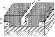
- FIG. 4Ais an overhead view of a nonplanar transistor 400 which has either a fully wrapped around gate electrode or a partially wrapped around gate electrode in accordance with embodiments of the present invention.
- FIG. 4Bis a cross-sectional view of FIG. 4A taken through the gate electrode when the gate electrode is partially wrapped around the channel region of the device.
- FIG. 4Cis a cross-sectional view of FIG. 4A taken through the gate electrode when the gate electrode is fully wrapped around the channel region of the device.
- the nonplanar device structureis ideal for use in a fully depleted substrate transistor application.
- the nonplanar device structureincludes a thin semiconductor body 408 formed on an insulating substrate 402 .
- a gate dielectric 422is formed on the top surface, sidewalls and on at least a portion of the bottom surface of the semiconductor body.
- a gate electrode 424is formed on the gate dielectric 422 on the top surface of the semiconductor body, is formed adjacent to the gate dielectric formed on the sidewalls of the semiconductor body and is formed beneath the gate dielectric formed on the bottom surface of the semiconductor body. Source and drain regions are formed in the semiconductor body 408 on opposite sides of the gate electrode 424 .
- the semiconductor bodycan be easily fully depleted when the transistor is turned “ON” thereby enabling the formation of a fully depleted transistor with gate lengths less than 30 nanometers without requiring the use of ultrathin semiconductor bodies or requiring photolithographic patterning of the semiconductor bodies to dimensions less than the gate length (Lg) of the device. That is, the structure of the nonplanar transistor of the present invention enables a fully depleted transistor to be fabricated where the thickness of the semiconductor body and the width of the semiconductor body are equal to the gate length of the device.
- the novel nonplanar transistor of the present inventioncan be operated in a fully depleted manner, the device is characterized by ideal (i.e., very sharp) subthreshold slope (ideally 60 mV/decade at 25° C.) and a reduced drain induced barrier (DIBL) short channel effect of less than 100 mV/V and ideally about 60 mV/V which results in lower leakage current when the device is turned “OFF” resulting in lower power consumption.
- ideal subthreshold slopeideally 60 mV/decade at 25° C.
- DIBLdrain induced barrier
- Nonplanar transistor 400is formed on an insulating substrate 402 .
- insulating substrate 402includes a lower monocrystalline silicon substrate 404 upon which is formed in insulating layer 406 , such as a silicon dioxide film.
- Nonplanar transistor 400can be formed on any well-known insulating substrate such as substrates formed from silicon dioxide, nitrides, oxides, and sapphires.
- Nonplanar transistor 400includes a semiconductor body 408 .
- Semiconductor body 408provides the source region 430 , drain region 432 and channel region 450 of the device.
- Semiconductor body 408can be formed of any well-known semiconductor material, such as but not limited to silicon (Si), germanium (Ge), silicon germanium (Si x Ge y ), gallium arsenide (GaAs), InSb, GaP, GaSb and carbon nanotubes.
- Semiconductor body 408can be formed of any well-known material which can be reversibly altered from an insulating state to a conductive state by applying external electrical controls.
- Semiconductor body 408is ideally a single crystalline film when the best electrical performance of transistor 400 , is desired.
- semiconductor body 408is a single crystalline film when transistor 400 is used in high performance applications, such as in a high density circuit, such as a microprocessor.
- Semiconductor body 408can be a polycrystalline film when transistor 400 is used in applications requiring less stringent performance, such as in liquid crystal displays.
- Insulator 406insulates semiconductor body 408 from monocrystalline silicon substrate 402 .
- semiconductor body 408is formed from a single crystalline silicon film.
- Semiconductor body 408has a pair of laterally opposite sidewalls 410 and 412 separated by a distance which defines a semiconductor body width (Wsi) 414 . Additionally, semiconductor body 408 has a top surface 416 opposite a bottom surface 418 formed on substrate 402 . The distance between the top surface 416 and the bottom surface 418 defines a body height (Tsi) 420 . In an embodiment of the present invention the body height 420 is substantially equal to the body width (Wsi) 414 . In an embodiment of the present invention, the body 408 has a width 414 and height (Tsi) 420 less than 30 nanometers and ideally less than 20 nanometers. In an embodiment of the present invention, the body height 420 is between 1 ⁇ 2 the body width 414 to 2 times the body width 414 .
- Nonplanar device 400has a gate dielectric layer 422 .
- Gate dielectric layer 422is formed on and around three sides of the channel region 350 of semiconductor body 408 as well as on or subadjacent to at least a portion of the bottom surface 418 of the channel region 450 semiconductor body 408 as shown in FIGS. 4A-4C . In the partially overlap embodiment of the present invention, as shown in FIG.
- the gate dielectric layer 422is formed on or adjacent to sidewall 412 , on top surface 416 , on or adjacent to sidewall 410 and is formed on a portion of the bottom surface 418 of semiconductor body 418 which extends from sidewall 412 towards the center of the bottom surface and covers a second portion which extends from sidewall 410 towards the center portion of the bottom surface 418 .
- the gate dielectric layer 422covers at least the lower corners 423 of the semiconductor body 408 and in another embodiment extends about 1 ⁇ 3 the width of semiconductor body 408 on each side. In the fully wrapped around embodiment shown in FIG.
- the gate dielectric layer 422is formed on or adjacent to sidewall 412 , on the top surface 416 , on or adjacent to sidewall 410 , and on the entire bottom surface 418 of the channel region of semiconductor body 408 .
- Gate dielectric layer 422can be any well-known gate dielectric layer.
- the gate dielectric layeris a silicon dioxide (SiO 2 ), silicon oxynitride (SiO x N y ) or a silicon nitride (Si 3 N 4 ) dielectric layer.
- the gate dielectric layer 422is a silicon oxynitride film formed to a thickness of between 5-20 ⁇ .
- gate dielectric layer 422is a high K gate dielectric layer, such as a metal oxide dielectric, such as but not limited to tantalum pentoxide (Ta 2 O 5 ), titanium oxide (TiO 2 ), hafnium oxide (HfO 2 ), HfSiO x N y , zirconium oxide (ZrO 2 ) and lanthanum oxide (LaO 2 ).
- Gate dielectric layer 422can be other types of high K dielectric, such as but not limited to PZT.
- Nonplanar device 400has a gate electrode 424 .
- Gate electrode 424is formed on and around gate dielectric layer 422 as shown in FIGS. 4A-4C .
- the gate electrode 424is formed on or adjacent the gate dielectric 424 formed on sidewall 412 of the channel region 450 of semiconductor body 408 , is formed on gate dielectric layer 422 formed on the top surface 416 of the channel region of semiconductor body 408 , is formed on or adjacent to gate dielectric layer 422 formed on sidewall 410 of the channel region of semiconductor body 408 , and is formed beneath or directly subadjacent to gate dielectric layer 422 formed beneath bottom surface 418 of the channel region of semiconductor body 408 .
- the gate electrode 424extends beneath bottom surface 418 approximately 1 ⁇ 3 the width of semiconductor body 408 on each side of the channel region 450 of the semiconductor body.
- the goalis to have the gate electrode wrap around the corners 423 of the device enough to provide good corner control.
- the remaining portion of the bottom surfaceis formed on buried insulating layer 406 .
- gate electrode 424is formed on or adjacent to gate dielectric layer 422 formed on sidewall 412 of the channel region of semiconductor body 408 , is formed on gate dielectric layer 422 formed on the top surface 416 of the channel region of semiconductor body 408 , is formed adjacent to or on the gate dielectric layer 422 formed on sidewall 410 of the channel region of semiconductor body 408 , and is formed beneath or directly subadjacent to the gate dielectric layer 422 formed on the channel region of semiconductor body 408 .
- Gate electrode 424has a pair of laterally opposite sidewalls 426 and 428 separated by a distance which defines the gate length (Lg) 430 of transistor 400 . In an embodiment of the present invention the laterally opposite sidewalls 426 and 428 of the gate electrode 424 run in a direction perpendicular to the laterally opposite sidewalls 410 and 412 of semiconductor body 408 .
- Gate electrode 424can be formed of any suitable gate electrode material.
- to gate electrode 424comprises of polycrystalline silicon doped to a concentration density between 1 ⁇ 10 19 atoms/cm 3 -1 ⁇ 10 21 atoms/cm 3 .
- the gate electrodecan be a metal gate electrode, such as but not limited to, tungsten, tantalum, titanium, and their nitrides.
- the gate electrodeis formed from a material having a work function compatible with the channel material (e.g., 4.0-5.2 eV for Si). It is to be appreciated, the gate electrode 424 need not necessarily be a single material and can be a composite stack of thin films, such as but not limited to a polycrystalline silicon/metal electrode or a metal/polycrystalline silicon electrode.
- Nonplanar transistor 400has a source region 430 and a drain region 432 .
- Source region 430 and drain region 432are formed in semiconductor body 408 on opposite sides of gate electrode 424 as shown in FIG. 4A .
- the source region 430 and the drain region 432are formed of the same conductivity type such as N-type or P-type conductivity.
- source region 430 and drain region 432have a doping concentration of between 1 ⁇ 10 19 and 1 ⁇ 10 21 atoms/cm 3 .
- Source region 430 and drain region 432can be formed of uniform concentration or can include subregions of different concentrations or doping profiles such as tip regions (e.g., source/drain extensions).
- source region 430 and drain region 432have the same doping concentration and profile.
- the doping concentration and profile of the source region 430 and the drain region 432may vary in order to obtain a particular electrical characteristic.
- the source and drain regionsmay also include epitaxial silicon regrowth and/or silicides for improved device performance.
- the portion of semiconductor body 408 located between source region 430 and drain region 432defines the channel region 450 of transistor 400 .
- the channel region 450can also be defined as the area of the semiconductor body 408 surrounded by the gate electrode 424 .
- the source/drain regionmay extend slightly beneath the gate electrode through, for example, diffusion to define a channel region slightly smaller than the gate electrode length (Lg).
- channel region 450is intrinsic or undoped monocrystalline silicon.
- channel region 450is doped monocrystalline silicon. When channel region 450 is doped it is typically doped to a conductivity level of between 1 ⁇ 10 16 to 1 ⁇ 10 19 atoms/cm 3 .
- the channel regionwhen the channel region is doped it is typically doped to the opposite conductivity type of the source region 430 and the drain region 432 .
- the channel region 450when the source and drain regions are N-type conductivity the channel region 450 would be doped to p type conductivity.
- the source and drain regionsare P type conductivity the channel region would be N-type conductivity.
- Channel region 450can be uniformly doped or can be doped non-uniformly or with differing concentrations to provide particular electrical and performance characteristics.
- channel regions 450can include well-known “halo” regions, if desired.
- the nonplanar transistorcan be characterized as having four channels and four gates, one gate (g 1 ) and channel which extends between the source and drain regions on side 412 of semiconductor body 408 , a second gate (g 2 ) and channel which extends between the source and drain regions on the top surface 416 of semiconductor body 408 , a third gate (g 3 ) and channel which extends between the source and drain regions on the sidewall 310 of semiconductor body 408 and a fourth channel and gate (g 4 ) between the source and drain regions on the bottom surface 418 of semiconductor body 408 .
- the gate “width” (Gw) of transistor 400is the sum of the widths of the four gates.
- the gate width of transistor 400is equal to the height 420 of silicon body 408 at sidewall 410 , plus the width of silicon body of 308 at the top surface 416 , plus the height 420 of silicon body 408 at sidewall 412 plus the amount of the bottom surface of semiconductor body 408 above gate electrode 424 .
- Larger “width” transistorscan be obtained by using multiple devices coupled together (e.g., multiple silicon bodies 408 surrounded by a single gate electrode 424 ).
- transistor 400can include an additional or multiple semiconductor bodies or fingers 408 as shown in FIG. 5 .
- Each semiconductor body 408has a gate dielectric layer 422 formed on its top surface and sidewalls and bottom surface or a portion of the bottom surface as shown in FIG. 5 .
- Gate electrode 424is formed on and adjacent to each gate dielectric 422 on each of the semiconductor bodies 408 .
- Each semiconductor body 408also includes a source region 430 and a drain region 432 formed in the semiconductor body 408 on opposite sides of gate electrode 424 as shown in FIG. 5 .
- each semiconductor body 408is formed with the same width and height (thickness) as the other semiconductor bodies 408 .
- each source regions 430 and drain regions 432 of the semiconductor bodies 408are electrically coupled together by source landing pad 560 and a drain landing pad 580 as shown in FIG. 5 .
- the source regions 430 and drain regions 432can be coupled together by higher levels of metallization (e.g., metal 1 , metal 2 , metal 3 . . . ) used to electrically interconnect various transistors 400 together into functional circuits.
- the gate width of transistor 400 as shown in FIG. 5is equal to the sum of the gate width created by each of the semiconductor bodies 408 . In this way, a tri-gate transistor 400 can be formed with any gate width desired.
- transistor 400can be operated in a fully depleted manner wherein when transistor 400 is turned “ON” the channel region 450 fully depletes thereby providing the advantageous electrical characteristics and performance of a fully depleted transistor. That is, when transistor 400 is turned “ON” a depletion region is formed in channel region 450 along with an inversion layer at the surfaces of region 450 (i.e., an inversion layer is formed on the side surfaces 410 and 412 and on top surface 416 and on bottom surface 418 of the semiconductor body).
- the inversion layerhas the same conductivity type as the source and drain regions and forms a conductive channel between the source and drain regions to allow current to flow therebetween.
- the depletion regiondepletes free carriers from beneath the inversion layers.
- the entire channel region 450 except for the inversion layeris depleted of carriers, thus the transistor can be said to be a “fully depleted” transistor.
- Fully depleted transistorshave improved electrical performance characteristics over non-fully depleted or partially depleted transistors. For example, operating transistor 400 in a fully depleted manner, gives transistor 400 an ideal or very steep subthreshold slope.
- the nonplanar transistorcan be fabricated with very steep sub-threshold slope of less than 80 mV/decade, and ideally about 60 mV/decade even when fabricated with semiconductor body thicknesses of less than 30 nm.
- transistor 400has an improved drain induced barrier (DIBL) lowering effect which provides for better “OFF” state leakage which results in lower leakage and thereby lower power consumption.
- DIBLdrain induced barrier
- the tri-gate transistor 400has a DIBL effect of less than 100 mV/V and ideally less than 40 mV/V.
- FIG. 9is an illustration of two plots 902 and 904 which set forth the body height and body width which will produce either fully depleted (F.D) or partially depleted (P.D) nonplanar transistors having gate length (Lg) of 30 nm ( 902 ) and 20 nm ( 904 ) respectively.
- the body height, body width and gate lengthare chosen to have dimensions in which a fully depleted transistor will be formed.
- the nonplanar transistorhas a body height, body width and gate length such that a partially depleted transistor is formed.
- the nonplanar transistor of the present inventioncan be said to be a nonplanar transistor because the inversion layers of the channel region 450 are formed in both the horizontal and vertical directions in semiconductor body 408 .
- the semiconductor device of the present inventioncan also be considered a nonplanar device because the electric field from the gate electrode 424 is applied from both horizontal (g 2 and g 4 ) and vertical sides (g 1 and g 3 ).
- FIGS. 6A-6GA method of fabricating a nonplanar transistor with a partially or fully wrapped around gate electrode in accordance with embodiments of the present invention is illustrated in FIGS. 6A-6G .
- the method of FIGS. 6A-6Gcan be referred to as a subtractive fabrication process.
- the fabrication of a nonplanar transistorbegins with an insulating substrate 602 .
- a silicon or semiconductor film 608is formed on insulating substrate 602 as shown in FIG. 6A .
- insulating substrate 602includes a lower monocrystalline silicon substrate 604 and a top insulating layer 606 , such as a silicon dioxide film or silicon nitride film.
- Insulating layer 606isolates semiconductor film 608 from substrate 604 , and in embodiment is formed to a thickness between 200-2000 ⁇ . Insulating layer 606 is sometimes referred to as a “buried oxide” layer. When a silicon or semiconductor film 608 is formed on an insulating substrate 602 , a silicon or semiconductor on insulating (SOI) substrate is created.
- SOIsilicon or semiconductor on insulating
- semiconductor film 608is ideally a silicon film, in other embodiments it can be other types of semiconductor films, such as but not limited to germanium (Ge), a silicon germanium alloy (Si x Ge y ), gallium arsenide (GaAs), InSb, GaP, GaSb, as well as carbon nanotubes.
- semiconductor film 608is an intrinsic (i.e., undoped) silicon film.
- semiconductor film 608is doped to a p type or n type conductivity with a concentration level between 1 ⁇ 10 16 -1 ⁇ 10 19 atoms/cm 3 .
- Semiconductor film 608can be insitu doped (i.e., doped while it is deposited) or doped after it is formed on substrate 602 by for example ion-implantation. Doping after formation enables both PMOS and NMOS nonplanar devices to be fabricated easily on the same insulating substrate. The doping level of the semiconductor body at this point determines the doping level of the channel region of the device.
- Semiconductor film 608is formed to a thickness which is approximately equal to the height desired for the subsequently formed semiconductor body or bodies of the fabricated nonplanar transistor. In an embodiment of the present invention, semiconductor film 608 has a thickness or height 609 of less than 30 nanometers and ideally less than 20 nanometers. In an embodiment of the present invention, semiconductor film 608 is formed to the thickness approximately equal to the gate “length” desired of the fabricated nonplanar transistor. In an embodiment of the present invention, semiconductor film 608 is formed thicker than desired gate length of the device. In an embodiment of the present invention, semiconductor film 680 is formed to a thickness which will enable the fabricated nonplanar transistor to be operated in a fully depleted manner for its designed gate length (Lg).
- Lggate length
- Semiconductor film 608can be formed on insulating substrate 602 in any well-known method.
- a silicon on insulator substrateknown as the SIMOX technique
- oxygen atomsare implanted at a high dose into a single crystalline silicon substrate and then anneal to form the buried oxide 606 within the substrate.
- the portion of the single crystalline silicon substrate above the buried oxidebecomes the silicon film 608 .
- Another technique currently used to form SOI substratesis an epitaxial silicon film transfer technique which is generally referred to as bonded SOI.
- bonded SOIis an epitaxial silicon film transfer technique which is generally referred to as bonded SOI.
- a first silicon waferhas a thin oxide grown on its surface that will later serve as the buried oxide 606 in the SOI structure.
- a high dose hydrogen implantis made into the first silicon wafer to form a high stress region below the silicon surface of the first wafer.
- This first waferis then flipped over and bonded to the surface of a second silicon wafer.
- the first waferis then cleaved along the high stress plain created by the hydrogen implant. This results in a SOI structure with a thin silicon layer on top, the buried oxide underneath all on top of the single crystalline silicon substrate.
- Well-known smoothing techniquessuch as HCl smoothing or chemical mechanical polishing (CMP) can be used to smooth the top surface of semiconductor film 608 to its desired thickness.
- isolation regionscan be formed into SOI semiconductor film 608 in order to isolate the various transistors to be formed therein from one another. Isolation regions can be formed by etching away portions of the substrate film 608 surrounding a nonplanar transistor, by for example well-known photolithographic and etching techniques, and then back filling the etched regions with an insulating film, such as SiO 2 .
- the fin or body 620is patterned to have a width 618 which is equal to or greater than the width desired of the gate length (Lg) of the fabricated transistor. In this way, the most stringent photolithography constraints used to fabricate the transistor are associated with the gate electrode patterning and not the semiconductor body or fin definition.
- the semiconductor body or finswill have a width 618 less than or equal to 30 nanometers and ideally less than or equal to 20 nanometers.
- the semiconductor bodies or finshave a width 618 approximately equal to the silicon body height 609 .
- the fins or bodies 620have a width 618 which is between 1 ⁇ 2 the semiconductor body height 609 and two times the semiconductor body height 609 .
- the photolithography and etching stepcan be used to form multiple semiconductor bodies or fins, for a single transistor as shown in FIG. 5 . In this way, transistors with different gate widths (Gw) can be fabricated across a wafer.
- the photolithography and etching stepcan also be used to form source landing pads 622 and drain landing pads 624 from the semiconductor film in order to provide contact areas for the transistor. Additionally, the landing pads can be used to connect together the various source regions and to connect together the various drain regions when multiple semiconductor bodies are used in the nonplanar transistor.
- the semiconductor film 608can be patterned into fins and landing pads by well known photolithography and etching techniques which generally include the formation of a photoresist mask by masking, exposing, and developing a blanket deposited photoresist film, and then etching semiconductor film in alignment with the photoresist mask to form one or more silicon bodies or fins 620 and source and drain landing pads 622 and 624 respectively.
- Semiconductor film 608is etched until the underlying buried insulating layer 606 is exposed.
- Well-known semiconductor etching techniquessuch as anisotropic plasma etching or reactive ion etching can be used to etch semiconductor film 608 in alignment with the photoresist mask.
- semiconductor film 608is etched to form a semiconductor body or fin 620 (and source/drain landing pads 622 and 624 , if desired)
- the photoresist maskis removed by well-known techniques, such as by chemical stripping and O 2 ashing, to produce the substrate shown in FIG. 6B .
- a portion of the buried oxide layer 606 formed beneath semiconductor body 620is removed.
- a short isotropic oxide etchcan be performed to “undercut” the semiconductor body 620 and remove a portion or all of the buried oxide layer 606 beneath the semiconductor body 620 .
- the insulation etchremoves only a portion of the insulating film beneath the semiconductor body 620 .
- the etchremoves approximate 1 ⁇ 3 of the body width of the insulating film 606 from beneath each side of the semiconductor body 620 .
- the entire portion of the buried insulating layer 606is removed from beneath the semiconductor body 620 .
- the semiconductor body 620can be supported by source and drain landing pads 622 and 624 formed on the remaining portions of the buried insulating layer.
- Any well known isotropic oxide etchmay be utilized which is selective to the semiconductor material (i.e., an etch which can preferentially etch the insulating film 606 without significantly etching the semiconductor film 608 ).
- An etch with a selectivity of at least 10:1is desired.
- a buffered oxide etchBBE comprising hydrogen fluoride (HF) can be utilized.
- a gate dielectric layer 626is formed on and around each semiconductor body 620 . That is, a gate dielectric layer 626 is formed on the top surface 627 of semiconductor body 620 as well as on the laterally opposite sidewalls 628 and 629 of each of the semiconductor bodies 620 . When forming a partially wrapped around gate electrode, the gate dielectric 626 layer is formed on the exposed portion 631 of the underside of the semiconductor body 620 . When forming a completely wrapped around gate electrode, the gate dielectric layer is formed on the entire bottom surface of the exposed semiconductor body.
- the gate dielectriccan be a deposited dielectric or a grown dielectric.
- the gate dielectric layer 626should be formed by a conformal process which enables the formation of the dielectric 626 on the underside of the semiconductor body 620 .
- the gate dielectric layer 626is a silicon dioxide dielectric film grown with a dry/wet oxidation process.
- the silicon oxide filmis grown to a thickness of between 5-15 ⁇ .
- the gate dielectric film 626is a deposited dielectric, such as but not limited to a high dielectric constant film, such as metal oxide dielectric, such as tantalum pentoxide (Ta 2 O 5 ), titanium oxide (TiO 2 ), hafnium oxide (HfO 2 ), HfSiO x N y , zirconium oxide (ZrO 2 ) and lanthanum oxide (LaO 2 ) or other high-K dielectrics, such as PZT and BST formed by chemical vapor deposition (CVD) or atomic layer deposition (ALD).
- a high dielectric constant filmsuch as metal oxide dielectric, such as tantalum pentoxide (Ta 2 O 5 ), titanium oxide (TiO 2 ), hafnium oxide (HfO 2 ), HfSiO x N y , zirconium oxide (ZrO 2 ) and lanthanum oxide (LaO 2 ) or other high-K dielectrics, such as PZT and B
- a gate electrode material 630is blanket deposited over the substrate.
- the gate electrode 630is formed on the gate dielectric layer 626 formed on the top surface 627 of semiconductor body 620 and is formed on or adjacent to the gate dielectric 626 formed on or adjacent to the sidewalls 628 and 629 of the semiconductor body 620 and is formed beneath or subadjacent to the gate dielectric on the bottom of body 620 .
- the gate electrode material 630is formed by a conformal process, such as CVD or ALD, in order to ensure that gate electrode material can fill beneath the undercut portion of the semiconductor body so that the gate electrode can partially or fully wrap around the semiconductor body 608 .
- the gate electrode material 630can be deposited to a thickness between 200-3000 ⁇ .
- the gate electrode materialis deposited to a thickness or height sufficient to form a gate electrode with a height of at least three times the height 609 of semiconductor bodies 620 .
- the gate electrode materialcomprises polycrystalline silicon.
- the gate electrode materialcomprises a polycrystalline silicon germanium alloy.
- the gate electrode materialcan comprise a metal film, such as tungsten, tantalum, and their nitrides.
- a hard mask materialis deposited and defined into a patterned hard mask 632 which defines the location where the gate electrode is to be formed.
- the hard mask materialcan be formed of any material which will not be substantially etched while subsequently etching the gate electrode material into a gate electrode.
- the hard mask materialis silicon nitride formed to a thickness between 20-100 nanometers.
- the hard mask materialcan be formed into a patterned hard mask 634 using standard photolithography and etching techniques.
- the patterned hard mask 634is formed to a width which is desired for the electrode gate length of the device.
- the gate electrode materialis etched in alignment with the hard mask 634 to form a gate electrode 636 .
- the gate electrodeis first anisotropically etched in alignment with the hard mask to form a pair of laterally opposite sidewall 639 and 641 as shown in FIG. 6E .
- the anisotropic etchis continued until just about all of the unmasked gate electrode material 630 is removed and just before the buried insulating layer 606 is exposed.
- the anisotropic etchis continued until all of the unmasked gate electrode material is removed and the buried insulating layer 606 exposed.
- the anisotropic etchis performed with an appropriate etch which forms a passivating polymer film on the sidewall 639 and 641 of the gate electrode to help insure that vertical sidewalls in alignment with the hard mask 634 are formed.
- Any suitable anisotropic etch technique and etchantwhich can anisotropically etch the gate electrode material without substantially etching the hard mask and semiconductor film 608 can be used.
- a hard masksuch as silicon nitride can be used to pattern the semiconductor film into bodies and the hard mask left on during the gate patterning etch to protect the semiconductor body or bodies from etching during the gate etch.
- the distance between the laterally opposite sidewalls 639 and 641defines the gate length (Lg) of the device.
- the gate electrodecan be anisotropically etched and a passivating polymer film formed by a plasma etch utilizing a HBr/Cl 2 /O 2 chemistry.
- the etchis switched to an isotropic etch.
- the isotropic etchremoves the gate electrode material from regions underneath the semiconductor body where the gate electrode is not to be formed. It is important to remove the undesired portions of the gate electrode material from under the semiconductor body 620 so that “stringers” are not left which can short the source and drain regions to the gate electrode.
- the isotropic etch which is utilized to remove the “stringers”can be performed after the anisotropic etch completely etches down to the underlying insulating layer or can be done after the anisotropic etch almost reaches the underlying insulating layer.
- a polymer sidewall passivation on the gate electrodesprotects the gate electrode from laterally etching during the isotropic etch step.
- Some lateral undercutting 635 of the gate electrode 634may result near the bottom of the gate electrode but the passivated top portion of the gate electrode should maintain its original profile.
- the degree of undercuttingcan be controlled by modifying the amount of insulating layer undercutting and the depth of the recess into the insulating layer.
- the gate electrode 634is etched until the gate electrode is completely isolated from the semiconductor film 608 used to form the body 620 and source and drain region landing pads.
- the isotropic etchis conducted utilizing a hot phosphoric acid wet etch.
- the photolithography process used to define the hard mask and therefore the gate electrode 636utilizes a minimum or smallest dimension lithography process used to fabricate the nonplanar transistor. (That is, in an embodiment of the present invention the gate length (Lg) of the gate electrode 636 has a minimum feature dimension of the transistor defined by photolithography). In an embodiment of the present invention, the gate length is less than or equal to 30 nanometers and ideally less than or equal to 20 nanometers.
- Source 640 and drain 642 regions for the transistorare formed in semiconductor body 620 on opposite sides of gate electrode 630 as shown in FIG. 6G .
- Source and drain regions 640 and 642can be formed by placing dopants 644 into semiconductor bodies 620 on both sides 639 , 641 of gate electrode 630 in order to form regions 640 and 642 as shown in FIG. 6G . If source and drain landing pads 622 and 624 are utilized, they are also doped at this time.
- the semiconductor fin or body 620 on opposite sides of the gate electrodeare doped to a p type conductivity and to a concentration between 1 ⁇ 10 20 -1 ⁇ 10 21 atoms/cm 3 to form the source and drain regions.
- the semiconductor fin or body 620 on opposite sides of the gate electrodeis doped with n type conductivity ions to a concentration between 1 ⁇ 10 20 -1 ⁇ 10 21 atoms/cm 3 to form source and drain regions.
- the bodyis doped by ion-implantation.
- the ion-implantationoccurs in a vertical direction (i.e., a direction perpendicular to substrate 600 ) as shown in FIG. 6G .
- gate electrode 630is a polysilicon gate electrode, it can be doped during the ion-implantation process by first removing hard mask 634 .
- a polysilicon gate electrode 630will act as a mask to prevent the ion-implantation step from doping the channel region(s) 648 of the nonplanar transistor.
- the channel region 648is the portion of the semiconductor body 620 located beneath or surrounded by the gate electrode 636 .
- gate electrode 636is a metal electrode, the dielectric hard mask 634 can be used to block the doping during the ion-implantation process. In other embodiments, other methods, such as solid source diffusion, may be used to dope the semiconductor body to form source and drain extensions. At this point, fabrication of a nonplanar transistor with a partially or fully wrapped around gate electrode is complete.
- Halo regionscan be formed in silicon body prior to the formation of a source/drain regions or source/drain extension regions.
- Halo regionsare doped regions formed in the channel region 648 of the device and are of the same conductivity but of a slightly higher concentration than the doping of the channel region of the device.
- Halo regionscan be formed by ion-implanting dopants beneath the gate electrode by utilizing large angled ion-implantation techniques.
- the substrate shown in FIG. 6Gcan be further processed to form additional well known features, such as heavily doped source/drain contact regions, deposited silicon on the source and drain regions as well as the gate electrode, and the formation of silicide on the source/drain contact regions as well as on the gate electrode.
- FIGS. 7A-7Dillustrate a replacement gate method for forming a nonplanar transistor with an almost wrapper around or fully wrapped around gate electrode.
- the replacement gate techniqueis ideal for use when a metal gate electrode is desired.
- the replacement gate methodbegins with the same substrate and processing as shown in FIGS. 6A and 6B of the subtractive method described above.
- a dielectric film 702is blanket deposited over the semiconductor body and landing pads and over exposed portions of the buried insulating layer 608 .
- the insulating layeris formed to a thickness desired for the gate height.
- the insulating layer 702can be any suitable insulating layer, such as silicon nitride or silicon dioxide.
- the dielectric film 702is formed of a material which can be selectively etched with respect to the semiconductor film 608 . Additionally, the dielectric film ideally can be selectively etched with respect to the underlying buried insulating layer 606 .
- the insulating layer 702can be silicon nitride.
- the blanket deposited insulating film 702is then patterned with well known photolithography and etching techniques to form an opening or trench 704 in the dielectric film 702 which defines a location where the gate electrode is to be formed.
- the patterned insulating film 702forms a definition mask for the formation of the gate electrode by a damascene patterning approach.
- the dielectric film 702is etched with any suitable etchant which can anisotropically etch the dielectric film 702 without etching semiconductor body 620 .
- the insulating layer 702is etched until the underlying buried insulating layer 606 is exposed as well as the portion of the semiconductor body which is to provide the channel region of the device as shown in FIG. 7A .
- the opening 704is formed with a width 706 desired of the gate length (Lg) of the nonplanar transistor.
- the buried insulating layer 606is etched away from underneath the semiconductor body 620 to form an opening 705 which undercut the active channel region of the semiconductor body 620 as shown in FIG. 7B .
- the insulating layer undercut etchremoves a portion of the insulating layer from underneath each side of the semiconductor body.
- the undercut etchundercuts the semiconductor body by an amount which enables the subsequently formed gate electrode to wrap around at least the lower corners of the semiconductor body 620 and thereby control the current flow in the corners.
- the undercut etchwhen forming a nonplanar transistor with an almost wrapped around gate electrode, the undercut etch removes approximately 1 ⁇ 3 of the insulating layer beneath each side 628 and 629 of the semiconductor body 620 .
- the buried insulating layer undercut etchis continued until the entire insulating layer beneath the exposed portion (i.e., channel region) of the semiconductor body 620 is completely removed. Any well known isotropic etch which can etch the buried insulating layer without significantly etching the semiconductor body may be used.
- a wet etchcomprising buffered HF may be utilized to form undercut opening 705 . Additionally, as shown in FIG. 7B , the undercut etch will slightly undercut the patterned insulating layer 704 resulting in a slightly larger opening 705 and then trench 704 .
- a gate dielectric layer 624is formed on and around the exposed portion (i.e., channel region) of semiconductor body 620 as described above. That is, the gate dielectric layer is formed on the top surface of semiconductor body 620 , is formed on the sidewalls 628 and 629 of semiconductor body 620 and is formed beneath or subadjacent to the exposed portions of the underside 631 of the semiconductor body. In the case of a fully wrapped around gate electrode, the gate dielectric layer 624 is formed on the entire underside 631 of the channel region or the semiconductor body.
- the gate dielectric layermay be any suitable material and should be formed with a conformal deposition process, such as atomic layer deposition (ALD) or chemical vapor deposition (CVD) to insure sufficient formation of a gate dielectric layer on the underside 631 of semiconductor body 620 .
- ALDatomic layer deposition
- CVDchemical vapor deposition
- a gate electrode materialis blanket deposited over the substrate including on top of dielectric layer 702 and on top of and around the gate dielectric formed on and around semiconductor body 608 and onto insulating layer 608 .
- the gate electrode materialis deposited to a thickness sufficient to completely fill openings 705 and 706 .
- the gate electrode materialcan be any suitable material used to form a gate electrode such as described above.
- the gate electrode materialis a metal film, such as but not limited to tungsten (W), titanium nitride (TiN) and cobalt silicide (CoSi 2 ).
- the gate electrode materialshould be formed by a deposition technique, such as chemical vapor deposition (CVD) or atomic layer deposition (ALD) so that a conformal film is formed so that the entire trench opening 706 is filled as well as the undercut regions 705 beneath the semiconductor body 620 and the dielectric mask 702 .
- CVDchemical vapor deposition
- ALDatomic layer deposition
- planarization techniqueis utilized to remove excess gate material from the top of dielectric layer 702 so that a planarized top surface may be formed as shown in FIG. 7C .
- Any well known and suitable planarization techniques, such as chemical mechanical polishing or plasma etch backmay be utilized to remove the excess gate material from the top of the dielectric film 702 .
- source and drain regionsmay be formed by doping portions of the semiconductor body 620 as described above. This completes the fabrication of a nonplanar device having a partially or fully wrapped around gate electrode utilizing a replacement gate process. If desired, well known additional features, such as sidewall spacers, heavily source/drain contact regions, and silicide may be added at this time.
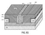
- FIG. 8A-8Gdescribe a method of forming a nonplanar device having a wrap around or fully wrapped around gate electrode whereby a replacement gate process is used after the formation of additional features, such as tip regions, spacer, additional semiconductors for ray source/drain regions and silicide on the source/drain regions.
- sacrificial gate oxide layer 802 and a sacrificial gate electrode 804are formed over the top surface and sidewalls of the silicon body 620 as shown in FIG. 8A .
- a sacrificial gate dielectric layer materialis blanket deposited over the substrate including the exposed surfaces of insulating layer 606 , the top surfaces and sidewalls of semiconductor body 620 and semiconductor landing pads 622 and 624 .
- a sacrificial gate electrode materialis blanket deposited over a substrate gate dielectric layer.
- the sacrificial gate electrode materialis deposited to a thickness desired for the height 805 of the subsequently formed gate electrode for the nonplanar device.
- the sacrificial gate electrode material and the sacrificial gate dielectric materialare then patterned by well known techniques, such as with photolithography and etching, to form the sacrificial gate electrode 804 and sacrificial gate dielectric 802 as shown in FIG. 8A .
- the sacrificial gate electrode and the sacrificial gate dielectricare patterned into the same shape and at the same location where the subsequently formed gate electrode and gate dielectric are to be formed.
- the sacrificial gate electrode materialis formed from a material, such as silicon nitride or polysilicon.
- tip or source/drain extensionscan be formed by doping the semiconductor body 620 on opposite sides of the sacrificial gate electrode 804 with impurities of the same conductivity type to be used to form a source/drain regions.
- the tip regionscan be formed by any well known technique, such as by ion implantation, which implants dopants 806 into the semiconductor body 620 as shown in FIG. 8A .
- the sacrificial gate 804prevents the channel region of the semiconductor body 620 from being doped during the tip formation step.
- tip regions having a doping concentration between 1 ⁇ 10 19 -1 ⁇ 10 21 atoms/cm 3are formed.
- dielectric sidewall spacers 808can be formed along opposite sidewalls of the sacrificial gate electrode 804 as shown in FIG. 8B .
- Sidewall spacerscan be formed by any well known technique, such as by blanket depositing a conformal sidewall spacer dielectric over the substrate including the top surface and sidewalls of the sacrificial gate electrode 804 as well as over the top surface and sidewalls of a semiconductor body 620 and landing pads 622 and 624 as well as onto the exposed surface of insulating substrate 602 .
- the dielectric spacer materialis deposited to a thickness which is approximately equal to the width desired for the spacers 808 .
- the dielectric spacer materialis deposited to a thickness between 20-100 nanometers.
- the spacer materialcan be silicon nitride, silicon oxide, silicon oxynitride or a combination thereof.
- the dielectric spacer materialis then anisotropically etched back to remove the dielectric spacer material from all horizontal surfaces (e.g., top surface of the sacrificial gate electrode 804 and the top surface of semiconductor body 620 and insulating layer 606 ) while leaving spacer material on vertical surfaces (e.g., the sidewalls of sacrificial gate electrode 804 ) to form sidewall spacers 808 as shown in FIG. 8B .
- an “over etch” of the anisotropic etch backcan be used to remove the spacer material from the sidewalls of the semiconductor body 620 and landing pads 622 and 622 while leaving sufficient spacer material to provide spacers 808 on the sidewalls of the sacrificial gate electrode 804 .
- additional silicon 810 and/or silicide 812can be formed onto the exposed top surface and sidewalls of the semiconductor body 620 and landing pads 622 and 624 .
- Additional siliconcan be formed on the exposed surface of the semiconductor body 620 by utilizing a selective deposition process.
- a selective silicon deposition processdeposits silicon, such as epitaxial silicon, onto silicon containing regions, such as semiconductor body 620 and landing pads 622 and 624 and does not deposit silicon on non-silicon containing areas, such as sacrificial gate electrode 804 , dielectric spacers 808 and insulating layer 606 . Any well known selective deposition process may be used to provide the additional epitaxial silicon. In an embodiment of the present invention, between 50-500 ⁇ of additional epitaxial silicon is selectively deposited onto semiconductor body 620 and landing pads 622 and 624 to form raised source/drain regions,
- heavy source/drain regionsmay be formed in the semiconductor body (and additional silicon, if used) on opposites of the gate electrode as well as into the landing pads 622 and 624 .
- Sidewall spacers 808prevent the underlying previously formed tip regions and the semiconductor body 620 from being doped by the heavy source/drain implant 810 .
- the sacrificial gate electrode 804masks the channel region from being doped during the heavy source/drain formation step.
- silicide 812such as but not limited to cobalt silicide, nickel silicide, and titanium silicide may be formed onto the exposed surfaces of the semiconductor body or onto the additionally added silicon film as shown in FIG. 8C .
- Silicidecan be formed onto the top surface and side surfaces of the exposed semiconductor body or additional silicon by utilizing a self-aligned or “salicide” process.
- a refractory metal filmsuch as but not limited to titanium, nickel and cobalt can be blanket deposited over the substrate including the silicon regions and dielectric regions.
- the substrateis then annealed to a temperature sufficient to cause the blanket deposited metal layer to react with the silicon containing regions to form a silicide. Regions, such as sidewalls spacers 808 , as well as insulating layer 606 will not react with the metal and the metal will remain unreacted metal in these areas.
- a selective wet etchcan be used to remove the unreacted metal while leaving the metal silicide 812 . In this way, silicide can be selectively formed only onto the silicon or semiconductor regions of a substrate as shown in FIG. 8C .
- a dielectric layer 814is blanket deposited over the substrate.
- the dielectric layeris formed to a thickness sufficient to completely cover the substrate including sacrificial gate electrode 804 .
- the dielectric layer 814is formed of a material which can be selectively etched with respect to the sacrificial gate material as well as semiconductor body 620 . That is, the dielectric material is formed of a material whereby the sacrificial gate electrode 804 can be removed without significantly etching away the dielectric layer 814 .
- the dielectric layeris planarized, such as chemical mechanical planarization until the top surface of the dielectric film is planar with the sacrificial gate electrode and the top surface of the sacrificial gate electrode exposed as shown in FIG. 8D .
- the sacrificial gate 804 and gate dielectric 802are etched out to form an opening 816 where the gate electrode is to be formed. Removing the sacrificial gate 808 and the sacrificial gate dielectric layer 802 exposes the channel region of the semiconductor body 620 of the nonplanar device as shown in FIG. 8E . Removal of the sacrificial gate electrode forms an opening 816 where the gate electrode is to be formed.
- the substrateis exposed to a undercut etch to form undercut opening 818 as described above.
- the undercut etchremoves a portion of the insulating layer 606 from beneath the channel region of semiconductor body 620 as shown in FIG. 8F .
- the undercut etchcan be used completely remove the insulating layer 606 from beneath the channel of semiconductor body 620 to expose the entire underside of the channel region of semiconductor body 620 in order to form a fully wrapped around gate electrode.
- the undercut etchmay remove only a portion of the insulating layer 606 from beneath each side of the channel region of semiconductor body 620 so that a partially wrapped around gate electrode can be fabricated as described above.
- gate dielectric 820 and a gate electrode 824are formed in openings 816 and 818 as shown in FIG. 8G .
- a gate dielectric film 820is blanket deposited over the substrate.
- the gate dielectric materialcovers the top surface and sidewalls of the channel region of the semiconductor body 620 as well as the exposed lower surfaces of the semiconductor body 620 as described above.
- the gate dielectric materialis formed by a conformal process, such as CVD or ALD, in order to ensure the formation of the gate dielectric material on the exposed underside of the channel region of the semiconductor body 620 .
- a gate electrode materialis blanket deposited over the gate dielectric.
- the gate electrode materialmay be any well known gate electrode material, such as described above.
- the gate electrode material and gate dielectricare then chemically mechanically planarized until the top surface of the dielectric layer 814 is revealed as shown in FIG. 8G .
- a gate electrode 824 and gate dielectric layer 820have been formed.
- the gate dielectric and gate electrodeeither partially or fully wraps around the channel region of the semiconductor body 620 as described above.
- Dielectric layer 814can left on the nonplanar device as shown in FIG. 8G and become part of the “back end” or interlayer dielectric (ILD) and metallization system used to electrically couple various nonplanar devices together into functional circuits.
- dielectric layer 814can be removed at this time and replaced by another type of interlayer dielectric for the “back end”. This completes this method of forming a nonplanar device having a fully wrapped around or partially wrapped around gate electrode.
Landscapes
- Thin Film Transistor (AREA)
- Insulated Gate Type Field-Effect Transistor (AREA)
- Container, Conveyance, Adherence, Positioning, Of Wafer (AREA)
- Electrical Discharge Machining, Electrochemical Machining, And Combined Machining (AREA)
- Junction Field-Effect Transistors (AREA)
Abstract
Description
This application is a divisional of U.S. patent application Ser. No. 10/607,769 filed Jun. 27, 2003, the entire contents of which are hereby incorporated by reference herein.
1. Field of the Invention
The present invention relates to the field of semiconductor integrated circuit manufacturing, and more particularly to a nonplanar fully depleted substrate transistor having a partially or fully wrapped around gate electrode and their methods of fabrication.
2. Discussion of Related Art
In order to increase device performance, silicon on insulator (SOI) transistors have been proposed for the fabrication of modern integrated circuits.FIG. 1 illustrates a standard fully depleted silicon on insulator (SOI)transistor 100.SOI transistor 100 includes a singlecrystalline silicon substrate 102 having aninsulating layer 104, such as a buried oxide formed thereon. A singlecrystalline silicon body 106 is formed on theinsulating layer 104. A gatedielectric layer 108 is formed on the singlecrystalline silicon body 106 and agate electrode 110 formed on the gate dielectric108.Source 112 anddrain 114 regions are formed in thesilicon body 106 along laterally opposite sides ofgate electrode 110.
Fully depleted SOI have been proposed as a transistor structure to take advantage of ideal sub-threshold gradients for optimized on current/off current ratios. In order to achieve ideal subthreshold gradients withtransistor 100, the thickness of thesilicon body 106 must be about ⅓ the size of the gate length (Lg) of the transistor or Tsi=Lg/3. However, as gate lengths scale especially as they approach 30 nm, the need for ever decreasing silicon film thickness (Tsi) makes this approach increasingly impractical. At 30 nanometer gate length, the thickness required of the silicon body is thought to need to be less than 10 nanometers, and around 6 nanometer for a 20 nanometer gate length. The fabrication of thin silicon films with thicknesses of less than 10 nanometers, is considered to be extremely difficult. On one hand, obtaining wafer uniformity on the order of one nanometer is a difficult challenge. On the other hand, to be able to contact these thin films to form raised source/drain regions to decrease junction resistance, becomes almost impossible since the thin silicon layer in the source/drain regions becomes consumed during the gate etch and various cleans following the gate etch and spacer etch leavinginsufficient silicon 106 for silicon to grow on.
A double gate (DG) device, such as shown inFIGS. 2A and 2B , have been proposed to alleviate the silicon thickness issue. The double gate (DG)device 200 includes asilicon body 202 formed on aninsulating substrate 204. A gate dielectric206 is formed on two sides of thesilicon body 202 and agate electrode 208 is formed adjacent to the gate dielectric206 formed on the two sides of thesilicon body 202. A sufficiently thickinsulating layer 209, such as silicon nitride, electrically isolates thegate electrode 208 from the top ofsilicon body 202.
Double gate (DG)device 200 essentially has two gates, one on either side of the channel of the device. Because thedouble gate device 200 has a gate on each side of the channel, thickness (Tsi) of the silicon body can be double that of a single gate device and still obtain a fully depleted transistor operation. That is, with a double gate device200 a fully depleted transistor can be formed where Tsi=(2×Lg)/3. The most manufacturable form of the double gate (DG)device 200, however, requires that thebody 202 patterning be done with photolithography that is 0.7× smaller than that used to pattern the gate length (Lg) of the device. In order to obtain high density integrated circuits, it is generally desirable to have the most aggressive lithography occur with respect to the gate length (Lg) of thegate electrode 208. Although, double gate structures double the thickness of the silicon film (since there now is a gate on either side of the channel) these structures, however, are hideously difficult to fabricate. For example,silicon body 202 requires a silicon body etch which can produce asilicon body 202 with an aspect ratio (height to width) of about 5:1.
The present invention is a novel nonplanar device structure which has a gate electrode which is fully wrapped around the channel region or gate electrode which is almost entirely wrapped around the channel region and their methods of fabrication. In following description numerous specific details are set forth in order to provide a thorough understanding of the present invention. In other instances, well known semiconductor processes and manufacturing techniques have not been described in particular detail in order to not unnecessarily obscure the present invention.
The present invention is a novel nonplanar transistor structure. In an embodiment of the present invention, the nonplanar transistor has a gate electrode which is fully wrapped around the channel region. In another embodiment of the present invention, the nonplanar transistor has a gate electrode which is partially or almost entirely wrapped around the channel region of the transistor. The advantage of a transistor having a gate electrode which is fully wrapped around the channel region or almost all around the channel region is that it is easier to deplete the channel region of the device and thereby relax the thickness (Tsi) and width (Wsi) dimensional constraints of the semiconductor body. Additionally, by completely or partially surrounding the channel of the device, the drive current of the device is enhanced by providing two additional corners in the device which increases carrier density.
Examples of anonplanar transistor 400 in accordance with embodiments of present invention are illustrated inFIG. 4A-4C .Nonplanar transistor 400 is formed on an insulatingsubstrate 402. In an embodiment of the present invention, insulatingsubstrate 402 includes a lowermonocrystalline silicon substrate 404 upon which is formed in insulatinglayer 406, such as a silicon dioxide film.Nonplanar transistor 400, however, can be formed on any well-known insulating substrate such as substrates formed from silicon dioxide, nitrides, oxides, and sapphires.
The portion ofsemiconductor body 408 located betweensource region 430 and drainregion 432, defines thechannel region 450 oftransistor 400. Thechannel region 450 can also be defined as the area of thesemiconductor body 408 surrounded by thegate electrode 424. At times however, the source/drain region may extend slightly beneath the gate electrode through, for example, diffusion to define a channel region slightly smaller than the gate electrode length (Lg). In an embodiment of the presentinvention channel region 450 is intrinsic or undoped monocrystalline silicon. In an embodiment of the present invention,channel region 450 is doped monocrystalline silicon. Whenchannel region 450 is doped it is typically doped to a conductivity level of between 1×10¹⁶to 1×10¹⁹atoms/cm3. In an embodiment of the present invention, when the channel region is doped it is typically doped to the opposite conductivity type of thesource region 430 and thedrain region 432. For example, when the source and drain regions are N-type conductivity thechannel region 450 would be doped to p type conductivity. Similarly, when the source and drain regions are P type conductivity the channel region would be N-type conductivity. In this manner anonplanar transistor 400 can be formed into either a NMOS transistor or a PMOS transistor respectively.Channel region 450 can be uniformly doped or can be doped non-uniformly or with differing concentrations to provide particular electrical and performance characteristics. For example,channel regions 450 can include well-known “halo” regions, if desired. When the transistor is turned “ON” current flows between thesource region 430 and the drain region through thegated channel region 450 in a direction parallel to the plane ofsubstrate 402.
By providing a gate dielectric and a gate electrode which surrounds the semiconductor body on all sides, the nonplanar transistor can be characterized as having four channels and four gates, one gate (g1) and channel which extends between the source and drain regions onside 412 ofsemiconductor body 408, a second gate (g2) and channel which extends between the source and drain regions on thetop surface 416 ofsemiconductor body 408, a third gate (g3) and channel which extends between the source and drain regions on the sidewall310 ofsemiconductor body 408 and a fourth channel and gate (g4) between the source and drain regions on thebottom surface 418 ofsemiconductor body 408. The gate “width” (Gw) oftransistor 400 is the sum of the widths of the four gates. That is, the gate width oftransistor 400 is equal to theheight 420 ofsilicon body 408 atsidewall 410, plus the width of silicon body of308 at thetop surface 416, plus theheight 420 ofsilicon body 408 atsidewall 412 plus the amount of the bottom surface ofsemiconductor body 408 abovegate electrode 424. Larger “width” transistors can be obtained by using multiple devices coupled together (e.g.,multiple silicon bodies 408 surrounded by a single gate electrode424).
As stated above the gate “width” oftransistor 400 is equal to the sum of the four gate widths created fromsemiconductor body 408 oftransistor 400. In order to fabricate the transistors with larger gate widths,transistor 400 can include an additional or multiple semiconductor bodies orfingers 408 as shown inFIG. 5 . Eachsemiconductor body 408 has agate dielectric layer 422 formed on its top surface and sidewalls and bottom surface or a portion of the bottom surface as shown inFIG. 5 .Gate electrode 424 is formed on and adjacent to eachgate dielectric 422 on each of thesemiconductor bodies 408. Eachsemiconductor body 408 also includes asource region 430 and adrain region 432 formed in thesemiconductor body 408 on opposite sides ofgate electrode 424 as shown inFIG. 5 . In an embodiment of the present invention eachsemiconductor body 408 is formed with the same width and height (thickness) as theother semiconductor bodies 408. In an embodiment of the present invention eachsource regions 430 anddrain regions 432 of thesemiconductor bodies 408 are electrically coupled together bysource landing pad 560 and adrain landing pad 580 as shown inFIG. 5 . Alternatively, thesource regions 430 anddrain regions 432 can be coupled together by higher levels of metallization (e.g., metal1,metal 2,metal 3 . . . ) used to electrically interconnectvarious transistors 400 together into functional circuits. The gate width oftransistor 400 as shown inFIG. 5 is equal to the sum of the gate width created by each of thesemiconductor bodies 408. In this way, atri-gate transistor 400 can be formed with any gate width desired.
Because thechannel region 450 is surrounded on all sides bygate electrode 424 andgate dielectric 422,transistor 400 can be operated in a fully depleted manner wherein whentransistor 400 is turned “ON” thechannel region 450 fully depletes thereby providing the advantageous electrical characteristics and performance of a fully depleted transistor. That is, whentransistor 400 is turned “ON” a depletion region is formed inchannel region 450 along with an inversion layer at the surfaces of region450 (i.e., an inversion layer is formed on the side surfaces410 and412 and ontop surface 416 and onbottom surface 418 of the semiconductor body). The inversion layer has the same conductivity type as the source and drain regions and forms a conductive channel between the source and drain regions to allow current to flow therebetween. The depletion region depletes free carriers from beneath the inversion layers. Theentire channel region 450 except for the inversion layer is depleted of carriers, thus the transistor can be said to be a “fully depleted” transistor. Fully depleted transistors have improved electrical performance characteristics over non-fully depleted or partially depleted transistors. For example, operatingtransistor 400 in a fully depleted manner, givestransistor 400 an ideal or very steep subthreshold slope. The nonplanar transistor can be fabricated with very steep sub-threshold slope of less than 80 mV/decade, and ideally about 60 mV/decade even when fabricated with semiconductor body thicknesses of less than 30 nm. Additionally, operatingtransistor 400 in the fully depleted manner,transistor 400 has an improved drain induced barrier (DIBL) lowering effect which provides for better “OFF” state leakage which results in lower leakage and thereby lower power consumption. In an embodiment of the present invention thetri-gate transistor 400 has a DIBL effect of less than 100 mV/V and ideally less than 40 mV/V.
The nonplanar transistor of the present invention can be said to be a nonplanar transistor because the inversion layers of thechannel region 450 are formed in both the horizontal and vertical directions insemiconductor body 408. The semiconductor device of the present invention can also be considered a nonplanar device because the electric field from thegate electrode 424 is applied from both horizontal (g2 and g4) and vertical sides (g1 and g3).
A method of fabricating a nonplanar transistor with a partially or fully wrapped around gate electrode in accordance with embodiments of the present invention is illustrated inFIGS. 6A-6G . The method ofFIGS. 6A-6G can be referred to as a subtractive fabrication process. The fabrication of a nonplanar transistor begins with an insulatingsubstrate 602. A silicon orsemiconductor film 608 is formed on insulatingsubstrate 602 as shown inFIG. 6A . In an embodiment of the present invention, insulatingsubstrate 602 includes a lowermonocrystalline silicon substrate 604 and a top insulatinglayer 606, such as a silicon dioxide film or silicon nitride film. Insulatinglayer 606 isolatessemiconductor film 608 fromsubstrate 604, and in embodiment is formed to a thickness between 200-2000 Å. Insulatinglayer 606 is sometimes referred to as a “buried oxide” layer. When a silicon orsemiconductor film 608 is formed on an insulatingsubstrate 602, a silicon or semiconductor on insulating (SOI) substrate is created.
Althoughsemiconductor film 608 is ideally a silicon film, in other embodiments it can be other types of semiconductor films, such as but not limited to germanium (Ge), a silicon germanium alloy (SixGey), gallium arsenide (GaAs), InSb, GaP, GaSb, as well as carbon nanotubes. In an embodiment of the present invention,semiconductor film 608 is an intrinsic (i.e., undoped) silicon film. In other embodiments,semiconductor film 608 is doped to a p type or n type conductivity with a concentration level between 1×10¹⁶-1×10¹⁹atoms/cm3.Semiconductor film 608 can be insitu doped (i.e., doped while it is deposited) or doped after it is formed onsubstrate 602 by for example ion-implantation. Doping after formation enables both PMOS and NMOS nonplanar devices to be fabricated easily on the same insulating substrate. The doping level of the semiconductor body at this point determines the doping level of the channel region of the device.
At this time, if desired, isolation regions (not shown) can be formed intoSOI semiconductor film 608 in order to isolate the various transistors to be formed therein from one another. Isolation regions can be formed by etching away portions of thesubstrate film 608 surrounding a nonplanar transistor, by for example well-known photolithographic and etching techniques, and then back filling the etched regions with an insulating film, such as SiO2.
Next, standard photolithography and etching techniques are used to define a semiconductor body orfin 620 in thesemiconductor film 608 for the tri-gate transistor as shown inFIG. 6B . In an embodiment of the present invention, the fin orbody 620 is patterned to have awidth 618 which is equal to or greater than the width desired of the gate length (Lg) of the fabricated transistor. In this way, the most stringent photolithography constraints used to fabricate the transistor are associated with the gate electrode patterning and not the semiconductor body or fin definition. In an embodiment of the present invention, the semiconductor body or fins will have awidth 618 less than or equal to 30 nanometers and ideally less than or equal to 20 nanometers. In an embodiment of the present invention, the semiconductor bodies or fins have awidth 618 approximately equal to thesilicon body height 609. In an embodiment of the present invention, the fins orbodies 620 have awidth 618 which is between ½ thesemiconductor body height 609 and two times thesemiconductor body height 609.
Additionally, the photolithography and etching step can be used to form multiple semiconductor bodies or fins, for a single transistor as shown inFIG. 5 . In this way, transistors with different gate widths (Gw) can be fabricated across a wafer. The photolithography and etching step can also be used to formsource landing pads 622 anddrain landing pads 624 from the semiconductor film in order to provide contact areas for the transistor. Additionally, the landing pads can be used to connect together the various source regions and to connect together the various drain regions when multiple semiconductor bodies are used in the nonplanar transistor.
Thesemiconductor film 608 can be patterned into fins and landing pads by well known photolithography and etching techniques which generally include the formation of a photoresist mask by masking, exposing, and developing a blanket deposited photoresist film, and then etching semiconductor film in alignment with the photoresist mask to form one or more silicon bodies orfins 620 and source and drainlanding pads Semiconductor film 608 is etched until the underlying buried insulatinglayer 606 is exposed. Well-known semiconductor etching techniques, such as anisotropic plasma etching or reactive ion etching can be used to etchsemiconductor film 608 in alignment with the photoresist mask. Aftersemiconductor film 608 is etched to form a semiconductor body or fin620 (and source/drain landing pads FIG. 6B .
Next, as shown inFIG. 6C , a portion of the buriedoxide layer 606 formed beneathsemiconductor body 620 is removed. A short isotropic oxide etch can be performed to “undercut” thesemiconductor body 620 and remove a portion or all of the buriedoxide layer 606 beneath thesemiconductor body 620. In the fabrication of an almost wrapped around gate electrode, the insulation etch (undercut etch) removes only a portion of the insulating film beneath thesemiconductor body 620. In an embodiment of the present invention, the etch removes approximate ⅓ of the body width of the insulatingfilm 606 from beneath each side of thesemiconductor body 620. When forming a transistor with a fully wrapped around gate electrode, the entire portion of the buried insulatinglayer 606 is removed from beneath thesemiconductor body 620. In such a case, thesemiconductor body 620 can be supported by source and drainlanding pads film 606 without significantly etching the semiconductor film608). An etch with a selectivity of at least 10:1 is desired. When thesemiconductor film 608 is silicon and the insulatingfilm 606 is silicon oxide, a buffered oxide etch (BOE) comprising hydrogen fluoride (HF) can be utilized.
Next, a gate dielectric layer626 is formed on and around eachsemiconductor body 620. That is, a gate dielectric layer626 is formed on thetop surface 627 ofsemiconductor body 620 as well as on the laterally oppositesidewalls semiconductor bodies 620. When forming a partially wrapped around gate electrode, the gate dielectric626 layer is formed on the exposedportion 631 of the underside of thesemiconductor body 620. When forming a completely wrapped around gate electrode, the gate dielectric layer is formed on the entire bottom surface of the exposed semiconductor body. The gate dielectric can be a deposited dielectric or a grown dielectric. The gate dielectric layer626 should be formed by a conformal process which enables the formation of the dielectric626 on the underside of thesemiconductor body 620. In an embodiment of the present invention, the gate dielectric layer626 is a silicon dioxide dielectric film grown with a dry/wet oxidation process. In an embodiment of the present invention, the silicon oxide film is grown to a thickness of between 5-15 Å. In an embodiment of the present invention, the gate dielectric film626 is a deposited dielectric, such as but not limited to a high dielectric constant film, such as metal oxide dielectric, such as tantalum pentoxide (Ta2O5), titanium oxide (TiO2), hafnium oxide (HfO2), HfSiOxNy, zirconium oxide (ZrO2) and lanthanum oxide (LaO2) or other high-K dielectrics, such as PZT and BST formed by chemical vapor deposition (CVD) or atomic layer deposition (ALD).
Next, as also shown inFIG. 6D , agate electrode material 630 is blanket deposited over the substrate. Thegate electrode 630 is formed on the gate dielectric layer626 formed on thetop surface 627 ofsemiconductor body 620 and is formed on or adjacent to the gate dielectric626 formed on or adjacent to thesidewalls semiconductor body 620 and is formed beneath or subadjacent to the gate dielectric on the bottom ofbody 620. Thegate electrode material 630 is formed by a conformal process, such as CVD or ALD, in order to ensure that gate electrode material can fill beneath the undercut portion of the semiconductor body so that the gate electrode can partially or fully wrap around thesemiconductor body 608. Thegate electrode material 630 can be deposited to a thickness between 200-3000 Å. In an embodiment the gate electrode material is deposited to a thickness or height sufficient to form a gate electrode with a height of at least three times theheight 609 ofsemiconductor bodies 620. In embodiment of the present invention, the gate electrode material comprises polycrystalline silicon. In another embodiment of the present invention, the gate electrode material comprises a polycrystalline silicon germanium alloy. In yet other embodiment of the present invention, the gate electrode material can comprise a metal film, such as tungsten, tantalum, and their nitrides.
Next, as shown inFIG. 6D , a hard mask material is deposited and defined into a patterned hard mask632 which defines the location where the gate electrode is to be formed. The hard mask material can be formed of any material which will not be substantially etched while subsequently etching the gate electrode material into a gate electrode. In an embodiment of the present invention, the hard mask material is silicon nitride formed to a thickness between 20-100 nanometers. The hard mask material can be formed into a patternedhard mask 634 using standard photolithography and etching techniques. The patternedhard mask 634 is formed to a width which is desired for the electrode gate length of the device.
Next the gate electrode material is etched in alignment with thehard mask 634 to form agate electrode 636. In an embodiment of the present invention, the gate electrode is first anisotropically etched in alignment with the hard mask to form a pair of laterally oppositesidewall FIG. 6E . In an embodiment of the present invention, the anisotropic etch is continued until just about all of the unmaskedgate electrode material 630 is removed and just before the buried insulatinglayer 606 is exposed. In an alternative embodiment of the present invention, the anisotropic etch is continued until all of the unmasked gate electrode material is removed and the buried insulatinglayer 606 exposed. In an embodiment of the present invention, the anisotropic etch is performed with an appropriate etch which forms a passivating polymer film on thesidewall hard mask 634 are formed. Any suitable anisotropic etch technique and etchant which can anisotropically etch the gate electrode material without substantially etching the hard mask andsemiconductor film 608 can be used. When the semiconductor film and gate electrode are formed from the same material, such as silicon, a hard mask such as silicon nitride can be used to pattern the semiconductor film into bodies and the hard mask left on during the gate patterning etch to protect the semiconductor body or bodies from etching during the gate etch. The distance between the laterally oppositesidewalls
Next, as shown inFIG. 6F , after the anisotropic etch, the etch is switched to an isotropic etch. The isotropic etch removes the gate electrode material from regions underneath the semiconductor body where the gate electrode is not to be formed. It is important to remove the undesired portions of the gate electrode material from under thesemiconductor body 620 so that “stringers” are not left which can short the source and drain regions to the gate electrode. The isotropic etch which is utilized to remove the “stringers” can be performed after the anisotropic etch completely etches down to the underlying insulating layer or can be done after the anisotropic etch almost reaches the underlying insulating layer. A polymer sidewall passivation on the gate electrodes protects the gate electrode from laterally etching during the isotropic etch step. Some lateral undercutting635 of thegate electrode 634 may result near the bottom of the gate electrode but the passivated top portion of the gate electrode should maintain its original profile. The degree of undercutting can be controlled by modifying the amount of insulating layer undercutting and the depth of the recess into the insulating layer. Thegate electrode 634 is etched until the gate electrode is completely isolated from thesemiconductor film 608 used to form thebody 620 and source and drain region landing pads. In an embodiment of the present invention, the isotropic etch is conducted utilizing a hot phosphoric acid wet etch. In an embodiment of the present invention, the photolithography process used to define the hard mask and therefore thegate electrode 636 utilizes a minimum or smallest dimension lithography process used to fabricate the nonplanar transistor. (That is, in an embodiment of the present invention the gate length (Lg) of thegate electrode 636 has a minimum feature dimension of the transistor defined by photolithography). In an embodiment of the present invention, the gate length is less than or equal to 30 nanometers and ideally less than or equal to 20 nanometers.
Next,source 640 and drain642 regions for the transistor are formed insemiconductor body 620 on opposite sides ofgate electrode 630 as shown inFIG. 6G . Source anddrain regions dopants 644 intosemiconductor bodies 620 on bothsides gate electrode 630 in order to formregions FIG. 6G . If source and drainlanding pads body 620 on opposite sides of the gate electrode are doped to a p type conductivity and to a concentration between 1×10²⁰-1×10²¹atoms/cm3to form the source and drain regions. For a NMOS tri-gate transistor, the semiconductor fin orbody 620 on opposite sides of the gate electrode is doped with n type conductivity ions to a concentration between 1×10²⁰-1×10²¹atoms/cm3to form source and drain regions. In an embodiment of the present invention, the body is doped by ion-implantation. In an embodiment of the present invention, the ion-implantation occurs in a vertical direction (i.e., a direction perpendicular to substrate600) as shown inFIG. 6G . Whengate electrode 630 is a polysilicon gate electrode, it can be doped during the ion-implantation process by first removinghard mask 634. Apolysilicon gate electrode 630 will act as a mask to prevent the ion-implantation step from doping the channel region(s)648 of the nonplanar transistor. The channel region648 is the portion of thesemiconductor body 620 located beneath or surrounded by thegate electrode 636. Ifgate electrode 636 is a metal electrode, the dielectrichard mask 634 can be used to block the doping during the ion-implantation process. In other embodiments, other methods, such as solid source diffusion, may be used to dope the semiconductor body to form source and drain extensions. At this point, fabrication of a nonplanar transistor with a partially or fully wrapped around gate electrode is complete.
In embodiments of the present invention, “halo” regions can be formed in silicon body prior to the formation of a source/drain regions or source/drain extension regions. Halo regions are doped regions formed in the channel region648 of the device and are of the same conductivity but of a slightly higher concentration than the doping of the channel region of the device. Halo regions can be formed by ion-implanting dopants beneath the gate electrode by utilizing large angled ion-implantation techniques.
Additionally, if desired, the substrate shown inFIG. 6G can be further processed to form additional well known features, such as heavily doped source/drain contact regions, deposited silicon on the source and drain regions as well as the gate electrode, and the formation of silicide on the source/drain contact regions as well as on the gate electrode.
Next, the buried insulatinglayer 606 is etched away from underneath thesemiconductor body 620 to form anopening 705 which undercut the active channel region of thesemiconductor body 620 as shown inFIG. 7B . When forming a nonplanar transistor with an almost wrapped around gate electrode, the insulating layer undercut etch removes a portion of the insulating layer from underneath each side of the semiconductor body. In an embodiment of the present invention, the undercut etch undercuts the semiconductor body by an amount which enables the subsequently formed gate electrode to wrap around at least the lower corners of thesemiconductor body 620 and thereby control the current flow in the corners. In an embodiment of the present invention, when forming a nonplanar transistor with an almost wrapped around gate electrode, the undercut etch removes approximately ⅓ of the insulating layer beneath eachside semiconductor body 620. When forming a nonplanar device with a fully wrapped around gate electrode, the buried insulating layer undercut etch is continued until the entire insulating layer beneath the exposed portion (i.e., channel region) of thesemiconductor body 620 is completely removed. Any well known isotropic etch which can etch the buried insulating layer without significantly etching the semiconductor body may be used. When the buried insulating layer is silicon oxide and the semiconductor body is silicon, a wet etch comprising buffered HF may be utilized to form undercutopening 705. Additionally, as shown inFIG. 7B , the undercut etch will slightly undercut the patterned insulatinglayer 704 resulting in a slightlylarger opening 705 and then trench704.
Next, agate dielectric layer 624 is formed on and around the exposed portion (i.e., channel region) ofsemiconductor body 620 as described above. That is, the gate dielectric layer is formed on the top surface ofsemiconductor body 620, is formed on thesidewalls semiconductor body 620 and is formed beneath or subadjacent to the exposed portions of theunderside 631 of the semiconductor body. In the case of a fully wrapped around gate electrode, thegate dielectric layer 624 is formed on theentire underside 631 of the channel region or the semiconductor body. As described above, the gate dielectric layer may be any suitable material and should be formed with a conformal deposition process, such as atomic layer deposition (ALD) or chemical vapor deposition (CVD) to insure sufficient formation of a gate dielectric layer on theunderside 631 ofsemiconductor body 620.
Next, a gate electrode material is blanket deposited over the substrate including on top ofdielectric layer 702 and on top of and around the gate dielectric formed on and aroundsemiconductor body 608 and onto insulatinglayer 608. The gate electrode material is deposited to a thickness sufficient to completely fillopenings 705 and706. The gate electrode material can be any suitable material used to form a gate electrode such as described above. In an embodiment of the present invention, the gate electrode material is a metal film, such as but not limited to tungsten (W), titanium nitride (TiN) and cobalt silicide (CoSi2). The gate electrode material should be formed by a deposition technique, such as chemical vapor deposition (CVD) or atomic layer deposition (ALD) so that a conformal film is formed so that the entire trench opening706 is filled as well as theundercut regions 705 beneath thesemiconductor body 620 and thedielectric mask 702.
Next, a planarization technique is utilized to remove excess gate material from the top ofdielectric layer 702 so that a planarized top surface may be formed as shown inFIG. 7C . Any well known and suitable planarization techniques, such as chemical mechanical polishing or plasma etch back may be utilized to remove the excess gate material from the top of thedielectric film 702.
Next, as shown inFIG. 7D , thedielectric film 702 is removed. At this time, source and drain regions may be formed by doping portions of thesemiconductor body 620 as described above. This completes the fabrication of a nonplanar device having a partially or fully wrapped around gate electrode utilizing a replacement gate process. If desired, well known additional features, such as sidewall spacers, heavily source/drain contact regions, and silicide may be added at this time.
The process begins with the same substrate and processing as shown inFIGS. 6A and 6B . After the patterning of thesemiconductor film 608 to formsemiconductor body 620 orbodies 620 and source/drain landing pads gate oxide layer 802 and asacrificial gate electrode 804 are formed over the top surface and sidewalls of thesilicon body 620 as shown inFIG. 8A . In order to form the sacrificial gate dielectric and electrode, first a sacrificial gate dielectric layer material is blanket deposited over the substrate including the exposed surfaces of insulatinglayer 606, the top surfaces and sidewalls ofsemiconductor body 620 andsemiconductor landing pads height 805 of the subsequently formed gate electrode for the nonplanar device. The sacrificial gate electrode material and the sacrificial gate dielectric material are then patterned by well known techniques, such as with photolithography and etching, to form thesacrificial gate electrode 804 and sacrificial gate dielectric802 as shown inFIG. 8A . The sacrificial gate electrode and the sacrificial gate dielectric are patterned into the same shape and at the same location where the subsequently formed gate electrode and gate dielectric are to be formed. In an embodiment of the present invention, the sacrificial gate electrode material is formed from a material, such as silicon nitride or polysilicon.
Next, if desired, tip or source/drain extensions can be formed by doping thesemiconductor body 620 on opposite sides of thesacrificial gate electrode 804 with impurities of the same conductivity type to be used to form a source/drain regions. The tip regions can be formed by any well known technique, such as by ion implantation, whichimplants dopants 806 into thesemiconductor body 620 as shown inFIG. 8A . Thesacrificial gate 804 prevents the channel region of thesemiconductor body 620 from being doped during the tip formation step. In an embodiment of the present invention, tip regions having a doping concentration between 1×10¹⁹-1×10²¹atoms/cm3are formed.
Next, if desired,dielectric sidewall spacers 808 can be formed along opposite sidewalls of thesacrificial gate electrode 804 as shown inFIG. 8B . Sidewall spacers can be formed by any well known technique, such as by blanket depositing a conformal sidewall spacer dielectric over the substrate including the top surface and sidewalls of thesacrificial gate electrode 804 as well as over the top surface and sidewalls of asemiconductor body 620 andlanding pads substrate 602. The dielectric spacer material is deposited to a thickness which is approximately equal to the width desired for thespacers 808. In an embodiment of the present invention, the dielectric spacer material is deposited to a thickness between 20-100 nanometers. The spacer material can be silicon nitride, silicon oxide, silicon oxynitride or a combination thereof. The dielectric spacer material is then anisotropically etched back to remove the dielectric spacer material from all horizontal surfaces (e.g., top surface of thesacrificial gate electrode 804 and the top surface ofsemiconductor body 620 and insulating layer606) while leaving spacer material on vertical surfaces (e.g., the sidewalls of sacrificial gate electrode804) to formsidewall spacers 808 as shown inFIG. 8B . By making theheight 805 of asacrificial gate electrode 804 sufficiently taller (e.g., 3×) than the thickness or height of thesemiconductor body 620, an “over etch” of the anisotropic etch back can be used to remove the spacer material from the sidewalls of thesemiconductor body 620 andlanding pads spacers 808 on the sidewalls of thesacrificial gate electrode 804.
Next, as shown inFIG. 8C ,additional silicon 810 and/orsilicide 812 can be formed onto the exposed top surface and sidewalls of thesemiconductor body 620 andlanding pads semiconductor body 620 by utilizing a selective deposition process. A selective silicon deposition process deposits silicon, such as epitaxial silicon, onto silicon containing regions, such assemiconductor body 620 andlanding pads sacrificial gate electrode 804,dielectric spacers 808 and insulatinglayer 606. Any well known selective deposition process may be used to provide the additional epitaxial silicon. In an embodiment of the present invention, between 50-500 Å of additional epitaxial silicon is selectively deposited ontosemiconductor body 620 andlanding pads
Next, if desired, heavy source/drain regions may be formed in the semiconductor body (and additional silicon, if used) on opposites of the gate electrode as well as into thelanding pads Sidewall spacers 808 prevent the underlying previously formed tip regions and thesemiconductor body 620 from being doped by the heavy source/drain implant 810. Additionally, as before, thesacrificial gate electrode 804 masks the channel region from being doped during the heavy source/drain formation step.
Additionally, if desired,silicide 812, such as but not limited to cobalt silicide, nickel silicide, and titanium silicide may be formed onto the exposed surfaces of the semiconductor body or onto the additionally added silicon film as shown inFIG. 8C . Silicide can be formed onto the top surface and side surfaces of the exposed semiconductor body or additional silicon by utilizing a self-aligned or “salicide” process. In a self-aligned or “salicide” process, a refractory metal film, such as but not limited to titanium, nickel and cobalt can be blanket deposited over the substrate including the silicon regions and dielectric regions. The substrate is then annealed to a temperature sufficient to cause the blanket deposited metal layer to react with the silicon containing regions to form a silicide. Regions, such as sidewalls spacers808, as well as insulatinglayer 606 will not react with the metal and the metal will remain unreacted metal in these areas. Next, a selective wet etch can be used to remove the unreacted metal while leaving themetal silicide 812. In this way, silicide can be selectively formed only onto the silicon or semiconductor regions of a substrate as shown inFIG. 8C .
Next, as shown inFIG. 8D , adielectric layer 814 is blanket deposited over the substrate. The dielectric layer is formed to a thickness sufficient to completely cover the substrate includingsacrificial gate electrode 804. Thedielectric layer 814 is formed of a material which can be selectively etched with respect to the sacrificial gate material as well assemiconductor body 620. That is, the dielectric material is formed of a material whereby thesacrificial gate electrode 804 can be removed without significantly etching away thedielectric layer 814. After blanket depositing the dielectric, the dielectric layer is planarized, such as chemical mechanical planarization until the top surface of the dielectric film is planar with the sacrificial gate electrode and the top surface of the sacrificial gate electrode exposed as shown inFIG. 8D .
Next, as shown inFIG. 8E , thesacrificial gate 804 andgate dielectric 802 are etched out to form anopening 816 where the gate electrode is to be formed. Removing thesacrificial gate 808 and the sacrificialgate dielectric layer 802 exposes the channel region of thesemiconductor body 620 of the nonplanar device as shown inFIG. 8E . Removal of the sacrificial gate electrode forms anopening 816 where the gate electrode is to be formed.
Next, as shown inFIG. 8F , the substrate is exposed to a undercut etch to form undercutopening 818 as described above. The undercut etch removes a portion of the insulatinglayer 606 from beneath the channel region ofsemiconductor body 620 as shown inFIG. 8F . The undercut etch can be used completely remove the insulatinglayer 606 from beneath the channel ofsemiconductor body 620 to expose the entire underside of the channel region ofsemiconductor body 620 in order to form a fully wrapped around gate electrode. Alternatively, the undercut etch may remove only a portion of the insulatinglayer 606 from beneath each side of the channel region ofsemiconductor body 620 so that a partially wrapped around gate electrode can be fabricated as described above.
Next, asgate dielectric 820 and agate electrode 824 are formed inopenings FIG. 8G . First, agate dielectric film 820 is blanket deposited over the substrate. The gate dielectric material covers the top surface and sidewalls of the channel region of thesemiconductor body 620 as well as the exposed lower surfaces of thesemiconductor body 620 as described above. The gate dielectric material is formed by a conformal process, such as CVD or ALD, in order to ensure the formation of the gate dielectric material on the exposed underside of the channel region of thesemiconductor body 620. Next, a gate electrode material is blanket deposited over the gate dielectric. The gate electrode material may be any well known gate electrode material, such as described above. The gate electrode material and gate dielectric are then chemically mechanically planarized until the top surface of thedielectric layer 814 is revealed as shown inFIG. 8G . Once the gate electrode material and the gate dielectric material are polished back or removed from the topdielectric material 814, agate electrode 824 andgate dielectric layer 820 have been formed. The gate dielectric and gate electrode either partially or fully wraps around the channel region of thesemiconductor body 620 as described above.Dielectric layer 814 can left on the nonplanar device as shown inFIG. 8G and become part of the “back end” or interlayer dielectric (ILD) and metallization system used to electrically couple various nonplanar devices together into functional circuits. Alternatively,dielectric layer 814 can be removed at this time and replaced by another type of interlayer dielectric for the “back end”. This completes this method of forming a nonplanar device having a fully wrapped around or partially wrapped around gate electrode.
Thus, nonplanar transistors with partially or fully wrapped around gate electrodes and their methods of fabrication have been described.
Claims (3)
1. A method of forming a nonplanar transistor comprising:
forming a semiconductor body having a top surface and bottom surface and a pair of laterally opposite sidewalls on an insulating substrate;
forming a sacrificial gate electrode above said top surface of said semiconductor body and adjacent to said laterally opposite sidewalls of said semiconductor body, said sacrificial gate electrode having a pair of laterally opposite sidewalls;
placing dopants into said semiconductor body on opposite sides of said sacrificial gate electrode to form a pair of source/drain extensions on opposite sides of said gate electrode;
forming a pair of sidewall spacers along laterally opposite sidewalls of said sacrificial gate electrode;
forming silicon on said semiconductor body adjacent to said sidewall spacers;
placing dopants into said silicon and into said semiconductor body in alignment with said sidewall spacers;
forming a silicide on said silicon formed on said semiconductor body adjacent to said sidewall spacers;
forming a dielectric layer over said silicide, said sacrificial gate electrode and said sidewall spacers;
planarizing said dielectric layer until the top surface of said dielectric layer is planar with the top surface of said sacrificial gate electrode and said sacrificial gate electrode is exposed;
removing said sacrificial gate electrode to expose the channel region of said semiconductor body and said insulating substrate;
removing a portion of said insulating substrate in said opening beneath said semiconductor body to expose at least a portion of said bottom surface of said semiconductor body;
forming a gate dielectric layer on said top surface and said sidewalls of said semiconductor body in said opening and on said portion of said exposed bottom surface of said semiconductor body;
blanket depositing a gate electrode material on said gate dielectric layer and into said opening and on said gate dielectric layer on said top surface of said semiconductor body, adjacent to said gate dielectric on said sidewalls of said semiconductor body, and beneath said gate dielectric on said exposed portion of said bottom surface of said semiconductor body; and
removing said gate electrode material from the top surface of said dielectric film to form a gate electrode.
2. The method ofclaim 1 wherein semiconductor body is formed from single crystalline silicon.
3. The method ofclaim 2 wherein said insulating substrate comprises a lower monocrystalline silicon substrate and a top silicon insulating film.
Priority Applications (2)
| Application Number | Priority Date | Filing Date | Title |
|---|---|---|---|
| US12/259,464US7820513B2 (en) | 2003-06-27 | 2008-10-28 | Nonplanar semiconductor device with partially or fully wrapped around gate electrode and methods of fabrication |
| US12/893,753US8273626B2 (en) | 2003-06-27 | 2010-09-29 | Nonplanar semiconductor device with partially or fully wrapped around gate electrode and methods of fabrication |
Applications Claiming Priority (2)
| Application Number | Priority Date | Filing Date | Title |
|---|---|---|---|
| US10/607,769US7456476B2 (en) | 2003-06-27 | 2003-06-27 | Nonplanar semiconductor device with partially or fully wrapped around gate electrode and methods of fabrication |
| US12/259,464US7820513B2 (en) | 2003-06-27 | 2008-10-28 | Nonplanar semiconductor device with partially or fully wrapped around gate electrode and methods of fabrication |
Related Parent Applications (1)
| Application Number | Title | Priority Date | Filing Date |
|---|---|---|---|
| US10/607,769DivisionUS7456476B2 (en) | 2003-06-27 | 2003-06-27 | Nonplanar semiconductor device with partially or fully wrapped around gate electrode and methods of fabrication |
Related Child Applications (1)
| Application Number | Title | Priority Date | Filing Date |
|---|---|---|---|
| US12/893,753ContinuationUS8273626B2 (en) | 2003-06-27 | 2010-09-29 | Nonplanar semiconductor device with partially or fully wrapped around gate electrode and methods of fabrication |
Publications (2)
| Publication Number | Publication Date |
|---|---|
| US20090061572A1 US20090061572A1 (en) | 2009-03-05 |
| US7820513B2true US7820513B2 (en) | 2010-10-26 |
Family
ID=34103128
Family Applications (3)
| Application Number | Title | Priority Date | Filing Date |
|---|---|---|---|
| US10/607,769Expired - Fee RelatedUS7456476B2 (en) | 2003-06-27 | 2003-06-27 | Nonplanar semiconductor device with partially or fully wrapped around gate electrode and methods of fabrication |
| US12/259,464Expired - LifetimeUS7820513B2 (en) | 2003-06-27 | 2008-10-28 | Nonplanar semiconductor device with partially or fully wrapped around gate electrode and methods of fabrication |
| US12/893,753Expired - Fee RelatedUS8273626B2 (en) | 2003-06-27 | 2010-09-29 | Nonplanar semiconductor device with partially or fully wrapped around gate electrode and methods of fabrication |
Family Applications Before (1)
| Application Number | Title | Priority Date | Filing Date |
|---|---|---|---|
| US10/607,769Expired - Fee RelatedUS7456476B2 (en) | 2003-06-27 | 2003-06-27 | Nonplanar semiconductor device with partially or fully wrapped around gate electrode and methods of fabrication |
Family Applications After (1)
| Application Number | Title | Priority Date | Filing Date |
|---|---|---|---|
| US12/893,753Expired - Fee RelatedUS8273626B2 (en) | 2003-06-27 | 2010-09-29 | Nonplanar semiconductor device with partially or fully wrapped around gate electrode and methods of fabrication |
Country Status (8)
| Country | Link |
|---|---|
| US (3) | US7456476B2 (en) |
| EP (2) | EP1639649B1 (en) |
| CN (1) | CN100541797C (en) |
| AT (1) | ATE491229T1 (en) |
| AU (1) | AU2003301042A1 (en) |
| DE (1) | DE60335301D1 (en) |
| TW (1) | TWI241718B (en) |
| WO (1) | WO2005010994A1 (en) |
Cited By (39)
| Publication number | Priority date | Publication date | Assignee | Title |
|---|---|---|---|---|
| US20090261380A1 (en)* | 2008-04-17 | 2009-10-22 | Brent Alan Anderson | Transistors having asymetric strained source/drain portions |
| US20100025767A1 (en)* | 2008-08-01 | 2010-02-04 | Kabushiki Kaisha Toshiba | Semiconductor device |
| US20100237424A1 (en)* | 2009-03-19 | 2010-09-23 | International Business Machines Corporation | Replacement gate cmos |
| US20110049613A1 (en)* | 2009-09-01 | 2011-03-03 | Taiwan Semiconductor Manufacturing Company, Ltd. | Accumulation type finfet, circuits and fabrication method thereof |
| US20110233679A1 (en)* | 2010-03-25 | 2011-09-29 | Taiwan Semiconductor Manufacturing Company, Ltd. | Integrated circuit including finfets and methods for forming the same |
| US20120007051A1 (en)* | 2010-07-06 | 2012-01-12 | International Business Machines Corporation | Process for Forming a Surrounding Gate for a Nanowire Using a Sacrificial Patternable Dielectric |
| US8264021B2 (en) | 2009-10-01 | 2012-09-11 | Taiwan Semiconductor Manufacturing Company, Ltd. | Finfets and methods for forming the same |
| US8298925B2 (en) | 2010-11-08 | 2012-10-30 | Taiwan Semiconductor Manufacturing Company, Ltd. | Mechanisms for forming ultra shallow junction |
| US8305829B2 (en) | 2009-02-23 | 2012-11-06 | Taiwan Semiconductor Manufacturing Company, Ltd. | Memory power gating circuit for controlling internal voltage of a memory array, system and method for controlling the same |
| US8305790B2 (en) | 2009-03-16 | 2012-11-06 | Taiwan Semiconductor Manufacturing Company, Ltd. | Electrical anti-fuse and related applications |
| US8431453B2 (en) | 2011-03-31 | 2013-04-30 | Taiwan Semiconductor Manufacturing Company, Ltd. | Plasma doping to reduce dielectric loss during removal of dummy layers in a gate structure |
| US8440517B2 (en) | 2010-10-13 | 2013-05-14 | Taiwan Semiconductor Manufacturing Company, Ltd. | FinFET and method of fabricating the same |
| US8461015B2 (en) | 2009-07-08 | 2013-06-11 | Taiwan Semiconductor Manufacturing Company, Ltd. | STI structure and method of forming bottom void in same |
| US8472227B2 (en) | 2010-01-27 | 2013-06-25 | Taiwan Semiconductor Manufacturing Company, Ltd. | Integrated circuits and methods for forming the same |
| US8497528B2 (en) | 2010-05-06 | 2013-07-30 | Taiwan Semiconductor Manufacturing Company, Ltd. | Method for fabricating a strained structure |
| US8592915B2 (en) | 2011-01-25 | 2013-11-26 | Taiwan Semiconductor Manufacturing Company, Ltd. | Doped oxide for shallow trench isolation (STI) |
| US8603924B2 (en) | 2010-10-19 | 2013-12-10 | Taiwan Semiconductor Manufacturing Company, Ltd. | Methods of forming gate dielectric material |
| US8623728B2 (en) | 2009-07-28 | 2014-01-07 | Taiwan Semiconductor Manufacturing Company, Ltd. | Method for forming high germanium concentration SiGe stressor |
| US8629478B2 (en) | 2009-07-31 | 2014-01-14 | Taiwan Semiconductor Manufacturing Company, Ltd. | Fin structure for high mobility multiple-gate transistor |
| US8652932B2 (en) | 2012-04-17 | 2014-02-18 | International Business Machines Corporation | Semiconductor devices having fin structures, and methods of forming semiconductor devices having fin structures |
| US8759943B2 (en) | 2010-10-08 | 2014-06-24 | Taiwan Semiconductor Manufacturing Company, Ltd. | Transistor having notched fin structure and method of making the same |
| US8769446B2 (en) | 2010-11-12 | 2014-07-01 | Taiwan Semiconductor Manufacturing Company, Ltd. | Method and device for increasing fin device density for unaligned fins |
| US20140183643A1 (en)* | 2012-12-28 | 2014-07-03 | Taiwan Semiconductor Manufacturing Company, Ltd. | Transistors with Wrapped-Around Gates and Methods for Forming the Same |
| US8877602B2 (en) | 2011-01-25 | 2014-11-04 | Taiwan Semiconductor Manufacturing Company, Ltd. | Mechanisms of doping oxide for forming shallow trench isolation |
| US8912602B2 (en) | 2009-04-14 | 2014-12-16 | Taiwan Semiconductor Manufacturing Company, Ltd. | FinFETs and methods for forming the same |
| US8957482B2 (en) | 2009-03-31 | 2015-02-17 | Taiwan Semiconductor Manufacturing Company, Ltd. | Electrical fuse and related applications |
| US8980719B2 (en) | 2010-04-28 | 2015-03-17 | Taiwan Semiconductor Manufacturing Company, Ltd. | Methods for doping fin field-effect transistors |
| US9040393B2 (en) | 2010-01-14 | 2015-05-26 | Taiwan Semiconductor Manufacturing Company, Ltd. | Method of forming semiconductor structure |
| US9048181B2 (en) | 2010-11-08 | 2015-06-02 | Taiwan Semiconductor Manufacturing Company, Ltd. | Mechanisms for forming ultra shallow junction |
| US20150295070A1 (en)* | 2012-11-16 | 2015-10-15 | Institute of Microelectronics, Chinese Academy of Sciences | Finfet and method for manufacturing the same |
| US20150364603A1 (en)* | 2014-06-16 | 2015-12-17 | International Business Machines Corporation | Finfet and nanowire semiconductor devices with suspended channel regions and gate structures surrounding the suspended channel regions |
| US9257641B2 (en) | 2013-11-08 | 2016-02-09 | Industrial Technology Research Institute | Via structure, memory array structure, three-dimensional resistance memory and method of forming the same |
| US9349850B2 (en) | 2013-07-17 | 2016-05-24 | Taiwan Semiconductor Manufacturing Company, Ltd. | Thermally tuning strain in semiconductor devices |
| US9419098B2 (en) | 2013-05-30 | 2016-08-16 | Taiwan Semiconductor Manufacturing Company, Ltd. | Tuning strain in semiconductor devices |
| US9484462B2 (en) | 2009-09-24 | 2016-11-01 | Taiwan Semiconductor Manufacturing Company, Ltd. | Fin structure of fin field effect transistor |
| US9496338B2 (en) | 2015-03-17 | 2016-11-15 | International Business Machines Corporation | Wire-last gate-all-around nanowire FET |
| US20170221993A1 (en)* | 2016-02-02 | 2017-08-03 | International Business Machines Corporation | Strained silicon germanium fin with block source/drain epitaxy and improved overlay capacitance |
| US10185798B2 (en) | 2016-03-02 | 2019-01-22 | Samsung Electronics Co., Ltd. | Layout design system, semiconductor device using the layout design system, and fabricating method thereof |
| US20210098378A1 (en)* | 2015-06-26 | 2021-04-01 | Taiwan Semiconductor Manufacturing Company, Ltd. | Porogen Bonded Gap Filling Material in Semiconductor Manufacturing |
Families Citing this family (410)
| Publication number | Priority date | Publication date | Assignee | Title |
|---|---|---|---|---|
| US7473947B2 (en)* | 2002-07-12 | 2009-01-06 | Intel Corporation | Process for ultra-thin body SOI devices that incorporate EPI silicon tips and article made thereby |
| US7456476B2 (en) | 2003-06-27 | 2008-11-25 | Intel Corporation | Nonplanar semiconductor device with partially or fully wrapped around gate electrode and methods of fabrication |
| FR2858876B1 (en)* | 2003-08-12 | 2006-03-03 | St Microelectronics Sa | METHOD FOR FORMATION UNDER A THIN LAYER OF A FIRST MATERIAL OF PORTIONS OF ANOTHER MATERIAL AND / OR VACUUM ZONES |
| US6946377B2 (en)* | 2003-10-29 | 2005-09-20 | Texas Instruments Incorporated | Multiple-gate MOSFET device with lithography independent silicon body thickness and methods for fabricating the same |
| US6962843B2 (en)* | 2003-11-05 | 2005-11-08 | International Business Machines Corporation | Method of fabricating a finfet |
| KR100605497B1 (en)* | 2003-11-27 | 2006-07-28 | 삼성전자주식회사 | Methods of manufacturing SOHI substrates, methods of manufacturing semiconductor devices using the same, and semiconductor devices manufactured thereby |
| KR100598099B1 (en)* | 2004-02-24 | 2006-07-07 | 삼성전자주식회사 | Vertical channel fin field effect transistor with damascene gate and method of manufacturing same |
| KR100612415B1 (en)* | 2004-04-09 | 2006-08-16 | 삼성전자주식회사 | Transistor having all around channel region and manufacturing method thereof |
| US7153784B2 (en)* | 2004-04-20 | 2006-12-26 | Intel Corporation | Method for making a semiconductor device having a high-k gate dielectric layer and a metal gate electrode |
| DE102005026228B4 (en)* | 2004-06-08 | 2010-04-15 | Samsung Electronics Co., Ltd., Suwon | GAA type transistor and method of making the same |
| KR100541657B1 (en)* | 2004-06-29 | 2006-01-11 | 삼성전자주식회사 | Multi-gate transistor fabrication method and multi-gate transistor fabricated thereby |
| US7042009B2 (en) | 2004-06-30 | 2006-05-09 | Intel Corporation | High mobility tri-gate devices and methods of fabrication |
| US7098507B2 (en)* | 2004-06-30 | 2006-08-29 | Intel Corporation | Floating-body dynamic random access memory and method of fabrication in tri-gate technology |
| US20060086977A1 (en) | 2004-10-25 | 2006-04-27 | Uday Shah | Nonplanar device with thinned lower body portion and method of fabrication |
| US7598516B2 (en)* | 2005-01-07 | 2009-10-06 | International Business Machines Corporation | Self-aligned process for nanotube/nanowire FETs |
| US7518196B2 (en) | 2005-02-23 | 2009-04-14 | Intel Corporation | Field effect transistor with narrow bandgap source and drain regions and method of fabrication |
| US7858481B2 (en) | 2005-06-15 | 2010-12-28 | Intel Corporation | Method for fabricating transistor with thinned channel |
| US7547637B2 (en) | 2005-06-21 | 2009-06-16 | Intel Corporation | Methods for patterning a semiconductor film |
| US7279375B2 (en)* | 2005-06-30 | 2007-10-09 | Intel Corporation | Block contact architectures for nanoscale channel transistors |
| US7288802B2 (en)* | 2005-07-27 | 2007-10-30 | International Business Machines Corporation | Virtual body-contacted trigate |
| US7606499B2 (en)* | 2005-08-01 | 2009-10-20 | Massachusetts Institute Of Technology | Bidirectional transceiver assembly for POF application |
| US7348642B2 (en) | 2005-08-03 | 2008-03-25 | International Business Machines Corporation | Fin-type field effect transistor |
| US20070090416A1 (en) | 2005-09-28 | 2007-04-26 | Doyle Brian S | CMOS devices with a single work function gate electrode and method of fabrication |
| US7485503B2 (en) | 2005-11-30 | 2009-02-03 | Intel Corporation | Dielectric interface for group III-V semiconductor device |
| KR100707208B1 (en)* | 2005-12-24 | 2007-04-13 | 삼성전자주식회사 | Pin-pet of BAA structure and its manufacturing method |
| FR2895835B1 (en)* | 2005-12-30 | 2008-05-09 | Commissariat Energie Atomique | ACHIEVING A MULTI-BRANCH CHANNEL STRUCTURE OF A TRANSISTOR GRID AND MEANS FOR ISOLATING THIS GRID FROM THE SOURCE AND DRAIN REGIONS |
| KR100718149B1 (en)* | 2006-02-07 | 2007-05-14 | 삼성전자주식회사 | Gate-All-Around Semiconductor Device |
| US7638398B2 (en)* | 2006-03-31 | 2009-12-29 | Hynix Semiconductor Inc. | Semiconductor device with increased channel area and fabrication method thereof |
| KR100832017B1 (en)* | 2006-03-31 | 2008-05-26 | 주식회사 하이닉스반도체 | Semiconductor device increased channel area and method for manufacturing the same |
| JP2007299991A (en)* | 2006-05-01 | 2007-11-15 | Toshiba Corp | Semiconductor device and manufacturing method thereof |
| US7422960B2 (en) | 2006-05-17 | 2008-09-09 | Micron Technology, Inc. | Method of forming gate arrays on a partial SOI substrate |
| KR100718159B1 (en)* | 2006-05-18 | 2007-05-14 | 삼성전자주식회사 | Wire-type semiconductor device and its manufacturing method |
| US20080014689A1 (en)* | 2006-07-07 | 2008-01-17 | Texas Instruments Incorporated | Method for making planar nanowire surround gate mosfet |
| US8143646B2 (en) | 2006-08-02 | 2012-03-27 | Intel Corporation | Stacking fault and twin blocking barrier for integrating III-V on Si |
| US7537994B2 (en) | 2006-08-28 | 2009-05-26 | Micron Technology, Inc. | Methods of forming semiconductor devices, assemblies and constructions |
| US20080090348A1 (en)* | 2006-09-28 | 2008-04-17 | Chang Peter L D | Gate-assisted silicon-on-insulator on bulk wafer and its application to floating body cell memory and transistors |
| US8389976B2 (en)* | 2006-12-29 | 2013-03-05 | Intel Corporation | Methods of forming carbon nanotube transistors for high speed circuit operation and structures formed thereby |
| US7772048B2 (en)* | 2007-02-23 | 2010-08-10 | Freescale Semiconductor, Inc. | Forming semiconductor fins using a sacrificial fin |
| US7821061B2 (en)* | 2007-03-29 | 2010-10-26 | Intel Corporation | Silicon germanium and germanium multigate and nanowire structures for logic and multilevel memory applications |
| US7435636B1 (en) | 2007-03-29 | 2008-10-14 | Micron Technology, Inc. | Fabrication of self-aligned gallium arsenide MOSFETs using damascene gate methods |
| US7935599B2 (en)* | 2007-04-04 | 2011-05-03 | Sharp Laboratories Of America, Inc. | Nanowire transistor and method for forming same |
| US9299568B2 (en) | 2007-05-25 | 2016-03-29 | Cypress Semiconductor Corporation | SONOS ONO stack scaling |
| US7960243B2 (en)* | 2007-05-31 | 2011-06-14 | Freescale Semiconductor, Inc. | Method of forming a semiconductor device featuring a gate stressor and semiconductor device |
| US8304781B2 (en)* | 2007-08-24 | 2012-11-06 | Sharp Kabushiki Kaisha | Circuit board provided with monolithic circuit having thin film transistor on substrate, and display device having the circuit board |
| KR101263648B1 (en)* | 2007-08-31 | 2013-05-21 | 삼성전자주식회사 | Fin field effect transistor and method of manufacturing the same |
| TW200913162A (en)* | 2007-09-11 | 2009-03-16 | Univ Nat Chiao Tung | Nonvolatile memory device with nanowire channel and a method for fabricating the same |
| WO2009036273A2 (en)* | 2007-09-12 | 2009-03-19 | Arizona Board Of Regents For And On Behalf Of Arizona State University | Horizontally depleted metal semiconductor field effect transistor |
| FR2921757B1 (en) | 2007-09-28 | 2009-12-18 | Commissariat Energie Atomique | DOUBLE-GRID TRANSISTOR STRUCTURE WITH MULTI-BRANCH CHANNEL |
| US7781825B2 (en)* | 2007-10-18 | 2010-08-24 | Macronix International Co., Ltd. | Semiconductor device and method for manufacturing the same |
| US9431549B2 (en) | 2007-12-12 | 2016-08-30 | Cypress Semiconductor Corporation | Nonvolatile charge trap memory device having a high dielectric constant blocking region |
| US8030163B2 (en)* | 2007-12-26 | 2011-10-04 | Intel Corporation | Reducing external resistance of a multi-gate device using spacer processing techniques |
| CN101556922B (en)* | 2008-04-10 | 2010-07-28 | 北京大学 | A kind of nano ring gate MOSFET transistor and its preparation method |
| WO2009130629A1 (en)* | 2008-04-23 | 2009-10-29 | Nxp B.V. | A fin fet and a method of manufacturing a fin fet |
| US8362566B2 (en) | 2008-06-23 | 2013-01-29 | Intel Corporation | Stress in trigate devices using complimentary gate fill materials |
| US20100019322A1 (en)* | 2008-07-23 | 2010-01-28 | International Business Machines Corporation | Semiconductor device and method of manufacturing |
| JP5391688B2 (en)* | 2008-12-26 | 2014-01-15 | 富士通セミコンダクター株式会社 | Semiconductor device manufacturing method and semiconductor device |
| US7884004B2 (en)* | 2009-02-04 | 2011-02-08 | International Business Machines Corporation | Maskless process for suspending and thinning nanowires |
| JP2010225768A (en)* | 2009-03-23 | 2010-10-07 | Toshiba Corp | Semiconductor device |
| US8378715B2 (en) | 2009-04-14 | 2013-02-19 | Monolithic 3D Inc. | Method to construct systems |
| US8754533B2 (en) | 2009-04-14 | 2014-06-17 | Monolithic 3D Inc. | Monolithic three-dimensional semiconductor device and structure |
| US9509313B2 (en) | 2009-04-14 | 2016-11-29 | Monolithic 3D Inc. | 3D semiconductor device |
| US8058137B1 (en) | 2009-04-14 | 2011-11-15 | Monolithic 3D Inc. | Method for fabrication of a semiconductor device and structure |
| US8362800B2 (en) | 2010-10-13 | 2013-01-29 | Monolithic 3D Inc. | 3D semiconductor device including field repairable logics |
| US8384426B2 (en)* | 2009-04-14 | 2013-02-26 | Monolithic 3D Inc. | Semiconductor device and structure |
| US9577642B2 (en) | 2009-04-14 | 2017-02-21 | Monolithic 3D Inc. | Method to form a 3D semiconductor device |
| US8395191B2 (en) | 2009-10-12 | 2013-03-12 | Monolithic 3D Inc. | Semiconductor device and structure |
| US8405420B2 (en) | 2009-04-14 | 2013-03-26 | Monolithic 3D Inc. | System comprising a semiconductor device and structure |
| US8669778B1 (en) | 2009-04-14 | 2014-03-11 | Monolithic 3D Inc. | Method for design and manufacturing of a 3D semiconductor device |
| US8373439B2 (en) | 2009-04-14 | 2013-02-12 | Monolithic 3D Inc. | 3D semiconductor device |
| US20110199116A1 (en)* | 2010-02-16 | 2011-08-18 | NuPGA Corporation | Method for fabrication of a semiconductor device and structure |
| US7986042B2 (en) | 2009-04-14 | 2011-07-26 | Monolithic 3D Inc. | Method for fabrication of a semiconductor device and structure |
| US8362482B2 (en) | 2009-04-14 | 2013-01-29 | Monolithic 3D Inc. | Semiconductor device and structure |
| US8427200B2 (en) | 2009-04-14 | 2013-04-23 | Monolithic 3D Inc. | 3D semiconductor device |
| US9711407B2 (en) | 2009-04-14 | 2017-07-18 | Monolithic 3D Inc. | Method of manufacturing a three dimensional integrated circuit by transfer of a mono-crystalline layer |
| US20110031997A1 (en)* | 2009-04-14 | 2011-02-10 | NuPGA Corporation | Method for fabrication of a semiconductor device and structure |
| KR100956798B1 (en) | 2009-07-14 | 2010-05-11 | 국민대학교산학협력단 | Method of manufacturing multi-bit-per cell non-volatile memory cell and nor type memory architecture using thereof |
| US12027518B1 (en) | 2009-10-12 | 2024-07-02 | Monolithic 3D Inc. | 3D semiconductor devices and structures with metal layers |
| US10910364B2 (en) | 2009-10-12 | 2021-02-02 | Monolitaic 3D Inc. | 3D semiconductor device |
| US10043781B2 (en) | 2009-10-12 | 2018-08-07 | Monolithic 3D Inc. | 3D semiconductor device and structure |
| US11018133B2 (en) | 2009-10-12 | 2021-05-25 | Monolithic 3D Inc. | 3D integrated circuit |
| US8450804B2 (en) | 2011-03-06 | 2013-05-28 | Monolithic 3D Inc. | Semiconductor device and structure for heat removal |
| US10388863B2 (en) | 2009-10-12 | 2019-08-20 | Monolithic 3D Inc. | 3D memory device and structure |
| US10354995B2 (en) | 2009-10-12 | 2019-07-16 | Monolithic 3D Inc. | Semiconductor memory device and structure |
| US8476145B2 (en) | 2010-10-13 | 2013-07-02 | Monolithic 3D Inc. | Method of fabricating a semiconductor device and structure |
| US8581349B1 (en) | 2011-05-02 | 2013-11-12 | Monolithic 3D Inc. | 3D memory semiconductor device and structure |
| US11984445B2 (en) | 2009-10-12 | 2024-05-14 | Monolithic 3D Inc. | 3D semiconductor devices and structures with metal layers |
| US10366970B2 (en) | 2009-10-12 | 2019-07-30 | Monolithic 3D Inc. | 3D semiconductor device and structure |
| US8536023B2 (en) | 2010-11-22 | 2013-09-17 | Monolithic 3D Inc. | Method of manufacturing a semiconductor device and structure |
| US8742476B1 (en) | 2012-11-27 | 2014-06-03 | Monolithic 3D Inc. | Semiconductor device and structure |
| US9099424B1 (en) | 2012-08-10 | 2015-08-04 | Monolithic 3D Inc. | Semiconductor system, device and structure with heat removal |
| US11374118B2 (en) | 2009-10-12 | 2022-06-28 | Monolithic 3D Inc. | Method to form a 3D integrated circuit |
| US8148728B2 (en) | 2009-10-12 | 2012-04-03 | Monolithic 3D, Inc. | Method for fabrication of a semiconductor device and structure |
| US10157909B2 (en) | 2009-10-12 | 2018-12-18 | Monolithic 3D Inc. | 3D semiconductor device and structure |
| US8173993B2 (en)* | 2009-12-04 | 2012-05-08 | International Business Machines Corporation | Gate-all-around nanowire tunnel field effect transistors |
| US8097515B2 (en)* | 2009-12-04 | 2012-01-17 | International Business Machines Corporation | Self-aligned contacts for nanowire field effect transistors |
| US8455334B2 (en) | 2009-12-04 | 2013-06-04 | International Business Machines Corporation | Planar and nanowire field effect transistors |
| US8313990B2 (en) | 2009-12-04 | 2012-11-20 | International Business Machines Corporation | Nanowire FET having induced radial strain |
| US8384065B2 (en)* | 2009-12-04 | 2013-02-26 | International Business Machines Corporation | Gate-all-around nanowire field effect transistors |
| US8309991B2 (en)* | 2009-12-04 | 2012-11-13 | International Business Machines Corporation | Nanowire FET having induced radial strain |
| US8143113B2 (en)* | 2009-12-04 | 2012-03-27 | International Business Machines Corporation | Omega shaped nanowire tunnel field effect transistors fabrication |
| US8129247B2 (en) | 2009-12-04 | 2012-03-06 | International Business Machines Corporation | Omega shaped nanowire field effect transistors |
| CN102104069B (en)* | 2009-12-16 | 2012-11-21 | 中国科学院微电子研究所 | Fin type transistor structure and manufacturing method thereof |
| CN102117829B (en)* | 2009-12-30 | 2012-11-21 | 中国科学院微电子研究所 | Fin type transistor structure and manufacturing method thereof |
| US8722492B2 (en) | 2010-01-08 | 2014-05-13 | International Business Machines Corporation | Nanowire pin tunnel field effect devices |
| US8373230B1 (en) | 2010-10-13 | 2013-02-12 | Monolithic 3D Inc. | Method for fabrication of a semiconductor device and structure |
| US8026521B1 (en) | 2010-10-11 | 2011-09-27 | Monolithic 3D Inc. | Semiconductor device and structure |
| US8541819B1 (en) | 2010-12-09 | 2013-09-24 | Monolithic 3D Inc. | Semiconductor device and structure |
| US9099526B2 (en) | 2010-02-16 | 2015-08-04 | Monolithic 3D Inc. | Integrated circuit device and structure |
| US8492886B2 (en) | 2010-02-16 | 2013-07-23 | Monolithic 3D Inc | 3D integrated circuit with logic |
| US8461035B1 (en) | 2010-09-30 | 2013-06-11 | Monolithic 3D Inc. | Method for fabrication of a semiconductor device and structure |
| US8324940B2 (en) | 2010-04-13 | 2012-12-04 | International Business Machines Corporation | Nanowire circuits in matched devices |
| US8361907B2 (en) | 2010-05-10 | 2013-01-29 | International Business Machines Corporation | Directionally etched nanowire field effect transistors |
| US8324030B2 (en) | 2010-05-12 | 2012-12-04 | International Business Machines Corporation | Nanowire tunnel field effect transistors |
| US10217667B2 (en) | 2011-06-28 | 2019-02-26 | Monolithic 3D Inc. | 3D semiconductor device, fabrication method and system |
| US8901613B2 (en) | 2011-03-06 | 2014-12-02 | Monolithic 3D Inc. | Semiconductor device and structure for heat removal |
| US8642416B2 (en) | 2010-07-30 | 2014-02-04 | Monolithic 3D Inc. | Method of forming three dimensional integrated circuit devices using layer transfer technique |
| US9219005B2 (en) | 2011-06-28 | 2015-12-22 | Monolithic 3D Inc. | Semiconductor system and device |
| US9953925B2 (en) | 2011-06-28 | 2018-04-24 | Monolithic 3D Inc. | Semiconductor system and device |
| US8835231B2 (en) | 2010-08-16 | 2014-09-16 | International Business Machines Corporation | Methods of forming contacts for nanowire field effect transistors |
| US8268689B2 (en)* | 2010-08-23 | 2012-09-18 | International Business Machines Corporation | Multiple threshold voltages in field effect transistor devices |
| US8536563B2 (en) | 2010-09-17 | 2013-09-17 | International Business Machines Corporation | Nanowire field effect transistors |
| US8273610B2 (en) | 2010-11-18 | 2012-09-25 | Monolithic 3D Inc. | Method of constructing a semiconductor device and structure |
| US8163581B1 (en) | 2010-10-13 | 2012-04-24 | Monolith IC 3D | Semiconductor and optoelectronic devices |
| US11482440B2 (en) | 2010-12-16 | 2022-10-25 | Monolithic 3D Inc. | 3D semiconductor device and structure with a built-in test circuit for repairing faulty circuits |
| US10497713B2 (en) | 2010-11-18 | 2019-12-03 | Monolithic 3D Inc. | 3D semiconductor memory device and structure |
| US12362219B2 (en) | 2010-11-18 | 2025-07-15 | Monolithic 3D Inc. | 3D semiconductor memory device and structure |
| US11600667B1 (en) | 2010-10-11 | 2023-03-07 | Monolithic 3D Inc. | Method to produce 3D semiconductor devices and structures with memory |
| US8114757B1 (en) | 2010-10-11 | 2012-02-14 | Monolithic 3D Inc. | Semiconductor device and structure |
| US11024673B1 (en) | 2010-10-11 | 2021-06-01 | Monolithic 3D Inc. | 3D semiconductor device and structure |
| US11018191B1 (en) | 2010-10-11 | 2021-05-25 | Monolithic 3D Inc. | 3D semiconductor device and structure |
| US11469271B2 (en) | 2010-10-11 | 2022-10-11 | Monolithic 3D Inc. | Method to produce 3D semiconductor devices and structures with memory |
| US11158674B2 (en) | 2010-10-11 | 2021-10-26 | Monolithic 3D Inc. | Method to produce a 3D semiconductor device and structure |
| US10290682B2 (en) | 2010-10-11 | 2019-05-14 | Monolithic 3D Inc. | 3D IC semiconductor device and structure with stacked memory |
| US11227897B2 (en) | 2010-10-11 | 2022-01-18 | Monolithic 3D Inc. | Method for producing a 3D semiconductor memory device and structure |
| US11315980B1 (en) | 2010-10-11 | 2022-04-26 | Monolithic 3D Inc. | 3D semiconductor device and structure with transistors |
| US10896931B1 (en) | 2010-10-11 | 2021-01-19 | Monolithic 3D Inc. | 3D semiconductor device and structure |
| US11257867B1 (en) | 2010-10-11 | 2022-02-22 | Monolithic 3D Inc. | 3D semiconductor device and structure with oxide bonds |
| US12360310B2 (en) | 2010-10-13 | 2025-07-15 | Monolithic 3D Inc. | Multilevel semiconductor device and structure with oxide bonding |
| US11984438B2 (en) | 2010-10-13 | 2024-05-14 | Monolithic 3D Inc. | Multilevel semiconductor device and structure with oxide bonding |
| US11164898B2 (en) | 2010-10-13 | 2021-11-02 | Monolithic 3D Inc. | Multilevel semiconductor device and structure |
| US10943934B2 (en) | 2010-10-13 | 2021-03-09 | Monolithic 3D Inc. | Multilevel semiconductor device and structure |
| US8379458B1 (en) | 2010-10-13 | 2013-02-19 | Monolithic 3D Inc. | Semiconductor device and structure |
| US10833108B2 (en) | 2010-10-13 | 2020-11-10 | Monolithic 3D Inc. | 3D microdisplay device and structure |
| US10978501B1 (en) | 2010-10-13 | 2021-04-13 | Monolithic 3D Inc. | Multilevel semiconductor device and structure with waveguides |
| US11694922B2 (en) | 2010-10-13 | 2023-07-04 | Monolithic 3D Inc. | Multilevel semiconductor device and structure with oxide bonding |
| US11043523B1 (en) | 2010-10-13 | 2021-06-22 | Monolithic 3D Inc. | Multilevel semiconductor device and structure with image sensors |
| US11855114B2 (en) | 2010-10-13 | 2023-12-26 | Monolithic 3D Inc. | Multilevel semiconductor device and structure with image sensors and wafer bonding |
| US11163112B2 (en) | 2010-10-13 | 2021-11-02 | Monolithic 3D Inc. | Multilevel semiconductor device and structure with electromagnetic modulators |
| US11404466B2 (en) | 2010-10-13 | 2022-08-02 | Monolithic 3D Inc. | Multilevel semiconductor device and structure with image sensors |
| US11929372B2 (en) | 2010-10-13 | 2024-03-12 | Monolithic 3D Inc. | Multilevel semiconductor device and structure with image sensors and wafer bonding |
| US12080743B2 (en) | 2010-10-13 | 2024-09-03 | Monolithic 3D Inc. | Multilevel semiconductor device and structure with image sensors and wafer bonding |
| US10998374B1 (en) | 2010-10-13 | 2021-05-04 | Monolithic 3D Inc. | Multilevel semiconductor device and structure |
| US12094892B2 (en) | 2010-10-13 | 2024-09-17 | Monolithic 3D Inc. | 3D micro display device and structure |
| US9197804B1 (en) | 2011-10-14 | 2015-11-24 | Monolithic 3D Inc. | Semiconductor and optoelectronic devices |
| US11869915B2 (en) | 2010-10-13 | 2024-01-09 | Monolithic 3D Inc. | Multilevel semiconductor device and structure with image sensors and wafer bonding |
| US11133344B2 (en) | 2010-10-13 | 2021-09-28 | Monolithic 3D Inc. | Multilevel semiconductor device and structure with image sensors |
| US11063071B1 (en) | 2010-10-13 | 2021-07-13 | Monolithic 3D Inc. | Multilevel semiconductor device and structure with waveguides |
| US11327227B2 (en) | 2010-10-13 | 2022-05-10 | Monolithic 3D Inc. | Multilevel semiconductor device and structure with electromagnetic modulators |
| US11855100B2 (en) | 2010-10-13 | 2023-12-26 | Monolithic 3D Inc. | Multilevel semiconductor device and structure with oxide bonding |
| US10679977B2 (en) | 2010-10-13 | 2020-06-09 | Monolithic 3D Inc. | 3D microdisplay device and structure |
| US11605663B2 (en) | 2010-10-13 | 2023-03-14 | Monolithic 3D Inc. | Multilevel semiconductor device and structure with image sensors and wafer bonding |
| US11437368B2 (en) | 2010-10-13 | 2022-09-06 | Monolithic 3D Inc. | Multilevel semiconductor device and structure with oxide bonding |
| US8524546B2 (en) | 2010-10-22 | 2013-09-03 | International Business Machines Corporation | Formation of multi-height MUGFET |
| US8524545B2 (en) | 2010-10-22 | 2013-09-03 | International Business Machines Corporation | Simultaneous formation of FinFET and MUGFET |
| US8232164B2 (en) | 2010-10-29 | 2012-07-31 | International Business Machines Corporation | Damascene method of forming a semiconductor structure and a semiconductor structure with multiple fin-shaped channel regions having different widths |
| US11495484B2 (en) | 2010-11-18 | 2022-11-08 | Monolithic 3D Inc. | 3D semiconductor devices and structures with at least two single-crystal layers |
| US12068187B2 (en) | 2010-11-18 | 2024-08-20 | Monolithic 3D Inc. | 3D semiconductor device and structure with bonding and DRAM memory cells |
| US11784082B2 (en) | 2010-11-18 | 2023-10-10 | Monolithic 3D Inc. | 3D semiconductor device and structure with bonding |
| US11508605B2 (en) | 2010-11-18 | 2022-11-22 | Monolithic 3D Inc. | 3D semiconductor memory device and structure |
| US11735462B2 (en) | 2010-11-18 | 2023-08-22 | Monolithic 3D Inc. | 3D semiconductor device and structure with single-crystal layers |
| US11901210B2 (en) | 2010-11-18 | 2024-02-13 | Monolithic 3D Inc. | 3D semiconductor device and structure with memory |
| US11004719B1 (en) | 2010-11-18 | 2021-05-11 | Monolithic 3D Inc. | Methods for producing a 3D semiconductor memory device and structure |
| US11610802B2 (en) | 2010-11-18 | 2023-03-21 | Monolithic 3D Inc. | Method for producing a 3D semiconductor device and structure with single crystal transistors and metal gate electrodes |
| US11107721B2 (en) | 2010-11-18 | 2021-08-31 | Monolithic 3D Inc. | 3D semiconductor device and structure with NAND logic |
| US11443971B2 (en) | 2010-11-18 | 2022-09-13 | Monolithic 3D Inc. | 3D semiconductor device and structure with memory |
| US11482439B2 (en) | 2010-11-18 | 2022-10-25 | Monolithic 3D Inc. | Methods for producing a 3D semiconductor memory device comprising charge trap junction-less transistors |
| US11211279B2 (en) | 2010-11-18 | 2021-12-28 | Monolithic 3D Inc. | Method for processing a 3D integrated circuit and structure |
| US11094576B1 (en) | 2010-11-18 | 2021-08-17 | Monolithic 3D Inc. | Methods for producing a 3D semiconductor memory device and structure |
| US11521888B2 (en) | 2010-11-18 | 2022-12-06 | Monolithic 3D Inc. | 3D semiconductor device and structure with high-k metal gate transistors |
| US11482438B2 (en) | 2010-11-18 | 2022-10-25 | Monolithic 3D Inc. | Methods for producing a 3D semiconductor memory device and structure |
| US12272586B2 (en) | 2010-11-18 | 2025-04-08 | Monolithic 3D Inc. | 3D semiconductor memory device and structure with memory and metal layers |
| US11164770B1 (en) | 2010-11-18 | 2021-11-02 | Monolithic 3D Inc. | Method for producing a 3D semiconductor memory device and structure |
| US11355381B2 (en) | 2010-11-18 | 2022-06-07 | Monolithic 3D Inc. | 3D semiconductor memory device and structure |
| US11018042B1 (en) | 2010-11-18 | 2021-05-25 | Monolithic 3D Inc. | 3D semiconductor memory device and structure |
| US12154817B1 (en) | 2010-11-18 | 2024-11-26 | Monolithic 3D Inc. | Methods for producing a 3D semiconductor memory device and structure |
| US11862503B2 (en) | 2010-11-18 | 2024-01-02 | Monolithic 3D Inc. | Method for producing a 3D semiconductor device and structure with memory cells and multiple metal layers |
| US12144190B2 (en) | 2010-11-18 | 2024-11-12 | Monolithic 3D Inc. | 3D semiconductor device and structure with bonding and memory cells preliminary class |
| US11569117B2 (en) | 2010-11-18 | 2023-01-31 | Monolithic 3D Inc. | 3D semiconductor device and structure with single-crystal layers |
| US11923230B1 (en) | 2010-11-18 | 2024-03-05 | Monolithic 3D Inc. | 3D semiconductor device and structure with bonding |
| US12243765B2 (en) | 2010-11-18 | 2025-03-04 | Monolithic 3D Inc. | 3D semiconductor device and structure with metal layers and memory cells |
| US11355380B2 (en) | 2010-11-18 | 2022-06-07 | Monolithic 3D Inc. | Methods for producing 3D semiconductor memory device and structure utilizing alignment marks |
| US11031275B2 (en) | 2010-11-18 | 2021-06-08 | Monolithic 3D Inc. | 3D semiconductor device and structure with memory |
| US11854857B1 (en) | 2010-11-18 | 2023-12-26 | Monolithic 3D Inc. | Methods for producing a 3D semiconductor device and structure with memory cells and multiple metal layers |
| US12100611B2 (en) | 2010-11-18 | 2024-09-24 | Monolithic 3D Inc. | Methods for producing a 3D semiconductor device and structure with memory cells and multiple metal layers |
| US11615977B2 (en) | 2010-11-18 | 2023-03-28 | Monolithic 3D Inc. | 3D semiconductor memory device and structure |
| US11804396B2 (en) | 2010-11-18 | 2023-10-31 | Monolithic 3D Inc. | Methods for producing a 3D semiconductor device and structure with memory cells and multiple metal layers |
| US12033884B2 (en) | 2010-11-18 | 2024-07-09 | Monolithic 3D Inc. | Methods for producing a 3D semiconductor device and structure with memory cells and multiple metal layers |
| US12125737B1 (en) | 2010-11-18 | 2024-10-22 | Monolithic 3D Inc. | 3D semiconductor device and structure with metal layers and memory cells |
| US11121021B2 (en) | 2010-11-18 | 2021-09-14 | Monolithic 3D Inc. | 3D semiconductor device and structure |
| US12136562B2 (en) | 2010-11-18 | 2024-11-05 | Monolithic 3D Inc. | 3D semiconductor device and structure with single-crystal layers |
| US8633082B2 (en)* | 2010-11-23 | 2014-01-21 | International Business Machines Corporation | Method for fabricating high-gain MOSFETs with asymmetric source/drain doping for analog and RF applications |
| DE102010064283B4 (en)* | 2010-12-28 | 2012-12-27 | GLOBALFOUNDRIES Dresden Module One Ltd. Liability Company & Co. KG | A method of making a self-aligned land transistor on a bulk substrate by a late land etch |
| US8975670B2 (en) | 2011-03-06 | 2015-03-10 | Monolithic 3D Inc. | Semiconductor device and structure for heat removal |
| US8649209B1 (en)* | 2011-03-25 | 2014-02-11 | Altera Corporation | Memory element circuitry with reduced oxide definition width |
| US8853790B2 (en)* | 2011-04-05 | 2014-10-07 | International Business Machines Corporation | Semiconductor nanowire structure reusing suspension pads |
| US9041099B2 (en)* | 2011-04-11 | 2015-05-26 | Nanya Technology Corp. | Single-sided access device and fabrication method thereof |
| JP5325932B2 (en)* | 2011-05-27 | 2013-10-23 | 株式会社東芝 | Semiconductor device and manufacturing method thereof |
| US10388568B2 (en) | 2011-06-28 | 2019-08-20 | Monolithic 3D Inc. | 3D semiconductor device and system |
| CN102244102B (en)* | 2011-06-28 | 2013-06-12 | 复旦大学 | Electron tunneling based enclosure type grid control metal-insulator device |
| CN102956457B (en)* | 2011-08-22 | 2015-08-12 | 中国科学院微电子研究所 | Semiconductor device structure, manufacturing method thereof and semiconductor fin manufacturing method |
| US8969154B2 (en)* | 2011-08-23 | 2015-03-03 | Micron Technology, Inc. | Methods for fabricating semiconductor device structures and arrays of vertical transistor devices |
| CN103035708B (en)* | 2011-09-30 | 2015-11-25 | 中国科学院微电子研究所 | Semiconductor structure and manufacturing method thereof |
| US8687399B2 (en) | 2011-10-02 | 2014-04-01 | Monolithic 3D Inc. | Semiconductor device and structure |
| US8723272B2 (en)* | 2011-10-04 | 2014-05-13 | Taiwan Semiconductor Manufacturing Company, Ltd. | FinFET device and method of manufacturing same |
| US9029173B2 (en) | 2011-10-18 | 2015-05-12 | Monolithic 3D Inc. | Method for fabrication of a semiconductor device and structure |
| US8575013B2 (en)* | 2011-10-25 | 2013-11-05 | GlobalFoundries, Inc. | Replacement gate fabrication methods |
| KR101926356B1 (en) | 2011-12-06 | 2018-12-07 | 삼성전자주식회사 | Semiconductor device having back-bias region |
| WO2013095550A1 (en) | 2011-12-22 | 2013-06-27 | Intel Corporation | Semiconductor device having a necked semiconductor body and method of forming semiconductor bodies of varying width |
| US9281378B2 (en)* | 2012-01-24 | 2016-03-08 | Taiwan Semiconductor Manufacturing Company, Ltd. | Fin recess last process for FinFET fabrication |
| US9171925B2 (en) | 2012-01-24 | 2015-10-27 | Taiwan Semiconductor Manufacturing Company, Ltd. | Multi-gate devices with replaced-channels and methods for forming the same |
| US20130193513A1 (en)* | 2012-02-01 | 2013-08-01 | International Business Machines Corporation | Multi-Gate Field Effect Transistor with a Tapered Gate Profile |
| CN102544010B (en)* | 2012-02-28 | 2014-07-16 | 上海华力微电子有限公司 | Double-layered isolated three-dimensional array type semi-conductor nanowire MOSFET |
| US8809178B2 (en)* | 2012-02-29 | 2014-08-19 | Globalfoundries Inc. | Methods of forming bulk FinFET devices with replacement gates so as to reduce punch through leakage currents |
| US9000557B2 (en) | 2012-03-17 | 2015-04-07 | Zvi Or-Bach | Semiconductor device and structure |
| US10600888B2 (en) | 2012-04-09 | 2020-03-24 | Monolithic 3D Inc. | 3D semiconductor device |
| US11616004B1 (en) | 2012-04-09 | 2023-03-28 | Monolithic 3D Inc. | 3D semiconductor device and structure with metal layers and a connective path |
| US11410912B2 (en) | 2012-04-09 | 2022-08-09 | Monolithic 3D Inc. | 3D semiconductor device with vias and isolation layers |
| US11594473B2 (en) | 2012-04-09 | 2023-02-28 | Monolithic 3D Inc. | 3D semiconductor device and structure with metal layers and a connective path |
| US11881443B2 (en) | 2012-04-09 | 2024-01-23 | Monolithic 3D Inc. | 3D semiconductor device and structure with metal layers and a connective path |
| US11735501B1 (en) | 2012-04-09 | 2023-08-22 | Monolithic 3D Inc. | 3D semiconductor device and structure with metal layers and a connective path |
| US11476181B1 (en) | 2012-04-09 | 2022-10-18 | Monolithic 3D Inc. | 3D semiconductor device and structure with metal layers |
| US11694944B1 (en) | 2012-04-09 | 2023-07-04 | Monolithic 3D Inc. | 3D semiconductor device and structure with metal layers and a connective path |
| US11088050B2 (en) | 2012-04-09 | 2021-08-10 | Monolithic 3D Inc. | 3D semiconductor device with isolation layers |
| US8557632B1 (en) | 2012-04-09 | 2013-10-15 | Monolithic 3D Inc. | Method for fabrication of a semiconductor device and structure |
| US11164811B2 (en) | 2012-04-09 | 2021-11-02 | Monolithic 3D Inc. | 3D semiconductor device with isolation layers and oxide-to-oxide bonding |
| KR20130126036A (en)* | 2012-05-10 | 2013-11-20 | 삼성전자주식회사 | Semiconductor device including transistor |
| US9024355B2 (en)* | 2012-05-30 | 2015-05-05 | International Business Machines Corporation | Embedded planar source/drain stressors for a finFET including a plurality of fins |
| US20130320422A1 (en)* | 2012-05-31 | 2013-12-05 | International Business Machines Corporation | Finfet contacting a conductive strap structure of a dram |
| US9385131B2 (en) | 2012-05-31 | 2016-07-05 | Globalfoundries Inc. | Wrap-around fin for contacting a capacitor strap of a DRAM |
| US8809131B2 (en)* | 2012-07-17 | 2014-08-19 | International Business Machines Corporation | Replacement gate fin first wire last gate all around devices |
| US9041106B2 (en)* | 2012-09-27 | 2015-05-26 | Intel Corporation | Three-dimensional germanium-based semiconductor devices formed on globally or locally isolated substrates |
| US8716751B2 (en) | 2012-09-28 | 2014-05-06 | Intel Corporation | Methods of containing defects for non-silicon device engineering |
| US9093376B2 (en)* | 2012-10-24 | 2015-07-28 | International Business Machines Corporation | Replacement metal gate FinFET |
| CN103811320B (en)* | 2012-11-09 | 2017-08-11 | 中国科学院微电子研究所 | Semiconductor device and method for manufacturing the same |
| US9443962B2 (en) | 2012-11-09 | 2016-09-13 | Taiwan Semiconductor Manufacturing Company, Ltd. | Recessing STI to increase fin height in fin-first process |
| US8574929B1 (en) | 2012-11-16 | 2013-11-05 | Monolithic 3D Inc. | Method to form a 3D semiconductor device and structure |
| US8686428B1 (en) | 2012-11-16 | 2014-04-01 | Monolithic 3D Inc. | Semiconductor device and structure |
| US8822320B2 (en)* | 2012-11-20 | 2014-09-02 | International Business Machines Corporation | Dense finFET SRAM |
| US8759874B1 (en) | 2012-11-30 | 2014-06-24 | Stmicroelectronics, Inc. | FinFET device with isolated channel |
| US20140151639A1 (en)* | 2012-12-03 | 2014-06-05 | International Business Machines Corporation | Nanomesh complementary metal-oxide-semiconductor field effect transistors |
| US8956942B2 (en) | 2012-12-21 | 2015-02-17 | Stmicroelectronics, Inc. | Method of forming a fully substrate-isolated FinFET transistor |
| US11063024B1 (en) | 2012-12-22 | 2021-07-13 | Monlithic 3D Inc. | Method to form a 3D semiconductor device and structure |
| US11018116B2 (en) | 2012-12-22 | 2021-05-25 | Monolithic 3D Inc. | Method to form a 3D semiconductor device and structure |
| US11309292B2 (en) | 2012-12-22 | 2022-04-19 | Monolithic 3D Inc. | 3D semiconductor device and structure with metal layers |
| US8674470B1 (en) | 2012-12-22 | 2014-03-18 | Monolithic 3D Inc. | Semiconductor device and structure |
| US11961827B1 (en) | 2012-12-22 | 2024-04-16 | Monolithic 3D Inc. | 3D semiconductor device and structure with metal layers |
| US12051674B2 (en) | 2012-12-22 | 2024-07-30 | Monolithic 3D Inc. | 3D semiconductor device and structure with metal layers |
| US11217565B2 (en) | 2012-12-22 | 2022-01-04 | Monolithic 3D Inc. | Method to form a 3D semiconductor device and structure |
| US11916045B2 (en) | 2012-12-22 | 2024-02-27 | Monolithic 3D Inc. | 3D semiconductor device and structure with metal layers |
| US11784169B2 (en) | 2012-12-22 | 2023-10-10 | Monolithic 3D Inc. | 3D semiconductor device and structure with metal layers |
| US11967583B2 (en) | 2012-12-22 | 2024-04-23 | Monolithic 3D Inc. | 3D semiconductor device and structure with metal layers |
| CN103022136B (en)* | 2012-12-26 | 2015-09-30 | 电子科技大学 | A kind of MOS transistor of T-shaped grid structure |
| US10600657B2 (en) | 2012-12-29 | 2020-03-24 | Monolithic 3D Inc | 3D semiconductor device and structure |
| US10903089B1 (en) | 2012-12-29 | 2021-01-26 | Monolithic 3D Inc. | 3D semiconductor device and structure |
| US11004694B1 (en) | 2012-12-29 | 2021-05-11 | Monolithic 3D Inc. | 3D semiconductor device and structure |
| US10892169B2 (en) | 2012-12-29 | 2021-01-12 | Monolithic 3D Inc. | 3D semiconductor device and structure |
| US12249538B2 (en) | 2012-12-29 | 2025-03-11 | Monolithic 3D Inc. | 3D semiconductor device and structure including power distribution grids |
| US10651054B2 (en) | 2012-12-29 | 2020-05-12 | Monolithic 3D Inc. | 3D semiconductor device and structure |
| US11087995B1 (en) | 2012-12-29 | 2021-08-10 | Monolithic 3D Inc. | 3D semiconductor device and structure |
| US11430668B2 (en) | 2012-12-29 | 2022-08-30 | Monolithic 3D Inc. | 3D semiconductor device and structure with bonding |
| US11177140B2 (en) | 2012-12-29 | 2021-11-16 | Monolithic 3D Inc. | 3D semiconductor device and structure |
| US9871034B1 (en) | 2012-12-29 | 2018-01-16 | Monolithic 3D Inc. | Semiconductor device and structure |
| US10115663B2 (en) | 2012-12-29 | 2018-10-30 | Monolithic 3D Inc. | 3D semiconductor device and structure |
| US9385058B1 (en) | 2012-12-29 | 2016-07-05 | Monolithic 3D Inc. | Semiconductor device and structure |
| US11430667B2 (en) | 2012-12-29 | 2022-08-30 | Monolithic 3D Inc. | 3D semiconductor device and structure with bonding |
| US8802512B2 (en)* | 2013-01-11 | 2014-08-12 | International Business Machines Corporation | Overlap capacitance nanowire |
| US9076813B1 (en) | 2013-01-15 | 2015-07-07 | Stc.Unm | Gate-all-around metal-oxide-semiconductor transistors with gate oxides |
| US20140231914A1 (en)* | 2013-02-19 | 2014-08-21 | Applied Materials, Inc. | Fin field effect transistor fabricated with hollow replacement channel |
| US8906759B2 (en)* | 2013-02-25 | 2014-12-09 | International Business Machines Corporation | Silicon nitride gate encapsulation by implantation |
| CN104008974A (en)* | 2013-02-26 | 2014-08-27 | 中国科学院微电子研究所 | Semiconductor device and method for manufacturing the same |
| US9006045B2 (en) | 2013-03-11 | 2015-04-14 | Globalfoundries Inc. | Transistor including a gate electrode extending all around one or more channel regions |
| US10325651B2 (en) | 2013-03-11 | 2019-06-18 | Monolithic 3D Inc. | 3D semiconductor device with stacked memory |
| US8902663B1 (en) | 2013-03-11 | 2014-12-02 | Monolithic 3D Inc. | Method of maintaining a memory state |
| US12094965B2 (en) | 2013-03-11 | 2024-09-17 | Monolithic 3D Inc. | 3D semiconductor device and structure with metal layers and memory cells |
| US11869965B2 (en) | 2013-03-11 | 2024-01-09 | Monolithic 3D Inc. | 3D semiconductor device and structure with metal layers and memory cells |
| US11935949B1 (en) | 2013-03-11 | 2024-03-19 | Monolithic 3D Inc. | 3D semiconductor device and structure with metal layers and memory cells |
| US11398569B2 (en) | 2013-03-12 | 2022-07-26 | Monolithic 3D Inc. | 3D semiconductor device and structure |
| US8994404B1 (en) | 2013-03-12 | 2015-03-31 | Monolithic 3D Inc. | Semiconductor device and structure |
| US11088130B2 (en) | 2014-01-28 | 2021-08-10 | Monolithic 3D Inc. | 3D semiconductor device and structure |
| US11923374B2 (en) | 2013-03-12 | 2024-03-05 | Monolithic 3D Inc. | 3D semiconductor device and structure with metal layers |
| US10840239B2 (en) | 2014-08-26 | 2020-11-17 | Monolithic 3D Inc. | 3D semiconductor device and structure |
| US12100646B2 (en) | 2013-03-12 | 2024-09-24 | Monolithic 3D Inc. | 3D semiconductor device and structure with metal layers |
| US10224279B2 (en) | 2013-03-15 | 2019-03-05 | Monolithic 3D Inc. | Semiconductor device and structure |
| US9117749B1 (en) | 2013-03-15 | 2015-08-25 | Monolithic 3D Inc. | Semiconductor device and structure |
| GB2526460B (en) | 2013-03-15 | 2018-08-01 | Intel Corp | Nanowire transistor fabrication with hardmask layers |
| US8859379B2 (en) | 2013-03-15 | 2014-10-14 | International Business Machines Corporation | Stress enhanced finFET devices |
| US20140264490A1 (en)* | 2013-03-18 | 2014-09-18 | International Business Machines Corporation | Replacement gate electrode with a self-aligned dielectric spacer |
| US10438856B2 (en) | 2013-04-03 | 2019-10-08 | Stmicroelectronics, Inc. | Methods and devices for enhancing mobility of charge carriers |
| US9111801B2 (en)* | 2013-04-04 | 2015-08-18 | Stmicroelectronics, Inc. | Integrated circuit devices and fabrication techniques |
| US11487928B2 (en) | 2013-04-15 | 2022-11-01 | Monolithic 3D Inc. | Automation for monolithic 3D devices |
| US11030371B2 (en) | 2013-04-15 | 2021-06-08 | Monolithic 3D Inc. | Automation for monolithic 3D devices |
| US11574109B1 (en) | 2013-04-15 | 2023-02-07 | Monolithic 3D Inc | Automation methods for 3D integrated circuits and devices |
| US11720736B2 (en) | 2013-04-15 | 2023-08-08 | Monolithic 3D Inc. | Automation methods for 3D integrated circuits and devices |
| US9021414B1 (en) | 2013-04-15 | 2015-04-28 | Monolithic 3D Inc. | Automation for monolithic 3D devices |
| US11270055B1 (en) | 2013-04-15 | 2022-03-08 | Monolithic 3D Inc. | Automation for monolithic 3D devices |
| US11341309B1 (en) | 2013-04-15 | 2022-05-24 | Monolithic 3D Inc. | Automation for monolithic 3D devices |
| US9263455B2 (en) | 2013-07-23 | 2016-02-16 | Micron Technology, Inc. | Methods of forming an array of conductive lines and methods of forming an array of recessed access gate lines |
| TWI632688B (en)* | 2013-07-25 | 2018-08-11 | 半導體能源研究所股份有限公司 | Semiconductor device and method of manufacturing the same |
| US9349863B2 (en) | 2013-08-07 | 2016-05-24 | Globalfoundries Inc. | Anchored stress-generating active semiconductor regions for semiconductor-on-insulator finfet |
| US9219153B2 (en)* | 2013-08-21 | 2015-12-22 | Globalfoundries Inc. | Methods of forming gate structures for FinFET devices and the resulting semiconductor products |
| CN104576381B (en)* | 2013-10-14 | 2018-01-09 | 中国科学院微电子研究所 | Asymmetric ultrathin SOIMOS transistor structure and manufacturing method thereof |
| CN104576383B (en)* | 2013-10-14 | 2017-09-12 | 中国科学院微电子研究所 | FinFET structure and manufacturing method thereof |
| EP2866264A1 (en) | 2013-10-22 | 2015-04-29 | IMEC vzw | Method for manufacturing a field effect transistor of a non-planar type |
| US9252272B2 (en)* | 2013-11-18 | 2016-02-02 | Globalfoundries Inc. | FinFET semiconductor device having local buried oxide |
| JP6444714B2 (en)* | 2013-12-20 | 2018-12-26 | 株式会社半導体エネルギー研究所 | Method for manufacturing semiconductor device |
| US20150194433A1 (en)* | 2014-01-08 | 2015-07-09 | Broadcom Corporation | Gate substantial contact based one-time programmable device |
| US9508830B2 (en)* | 2014-01-23 | 2016-11-29 | Taiwan Semiconductor Manufacturing Company Limited | Method of forming FinFET |
| US12094829B2 (en) | 2014-01-28 | 2024-09-17 | Monolithic 3D Inc. | 3D semiconductor device and structure |
| US10297586B2 (en) | 2015-03-09 | 2019-05-21 | Monolithic 3D Inc. | Methods for processing a 3D semiconductor device |
| US11031394B1 (en) | 2014-01-28 | 2021-06-08 | Monolithic 3D Inc. | 3D semiconductor device and structure |
| US11107808B1 (en) | 2014-01-28 | 2021-08-31 | Monolithic 3D Inc. | 3D semiconductor device and structure |
| US9543407B2 (en)* | 2014-02-27 | 2017-01-10 | International Business Machines Corporation | Low-K spacer for RMG finFET formation |
| US10553718B2 (en)* | 2014-03-14 | 2020-02-04 | Taiwan Semiconductor Manufacturing Co., Ltd. | Semiconductor devices with core-shell structures |
| US9947772B2 (en) | 2014-03-31 | 2018-04-17 | Stmicroelectronics, Inc. | SOI FinFET transistor with strained channel |
| US9780213B2 (en) | 2014-04-15 | 2017-10-03 | Taiwan Semiconductor Manufacturing Co., Ltd. | Semiconductor device having a reversed T-shaped profile in the metal gate line-end |
| US9530659B2 (en) | 2014-05-02 | 2016-12-27 | International Business Machines Corporation | Structure for preventing buried oxide gouging during planar and FinFET Processing on SOI |
| CN105097913B (en)* | 2014-05-05 | 2018-12-04 | 中芯国际集成电路制造(上海)有限公司 | Field effect transistor and its manufacturing method |
| US9502518B2 (en) | 2014-06-23 | 2016-11-22 | Stmicroelectronics, Inc. | Multi-channel gate-all-around FET |
| US9659827B2 (en) | 2014-07-21 | 2017-05-23 | Samsung Electronics Co., Ltd. | Methods of manufacturing semiconductor devices by forming source/drain regions before gate electrode separation |
| TWI553869B (en)* | 2014-07-31 | 2016-10-11 | 瑞昱半導體股份有限公司 | Semiconductor component and multi-gate field effect transistor |
| US9306019B2 (en)* | 2014-08-12 | 2016-04-05 | GlobalFoundries, Inc. | Integrated circuits with nanowires and methods of manufacturing the same |
| US20160064371A1 (en)* | 2014-08-28 | 2016-03-03 | Globalfoundries Inc. | Non-planar esd device for non-planar output transistor and common fabrication thereof |
| US9543381B2 (en)* | 2014-09-11 | 2017-01-10 | Taiwan Semiconductor Manufacturing Company Ltd. | Semiconductor structure and manufacturing method of the same |
| US9773865B2 (en) | 2014-09-22 | 2017-09-26 | International Business Machines Corporation | Self-forming spacers using oxidation |
| US9064943B1 (en) | 2014-09-30 | 2015-06-23 | International Business Machines Corporation | Gate-all-around field effect transistor structures and methods |
| US9735256B2 (en)* | 2014-10-17 | 2017-08-15 | Taiwan Semiconductor Manufacturing Company, Ltd. | Method and structure for FinFET comprising patterned oxide and dielectric layer under spacer features |
| US9281379B1 (en) | 2014-11-19 | 2016-03-08 | International Business Machines Corporation | Gate-all-around fin device |
| CN104465354B (en)* | 2014-12-24 | 2017-11-07 | 上海集成电路研发中心有限公司 | All-around-gate pole structure and its manufacture method |
| US9502505B2 (en)* | 2014-12-31 | 2016-11-22 | Stmicroelectronics, Inc. | Method and structure of making enhanced UTBB FDSOI devices |
| US9929242B2 (en)* | 2015-01-12 | 2018-03-27 | Taiwan Semiconductor Manufacturing Co., Ltd. | Semiconductor device and manufacturing method thereof |
| US9502567B2 (en)* | 2015-02-13 | 2016-11-22 | Taiwan Semiconductor Manufacturing Co., Ltd. | Semiconductor fin structure with extending gate structure |
| CN105789306B (en)* | 2015-01-12 | 2020-12-08 | 台湾积体电路制造股份有限公司 | Semiconductor device and method of manufacturing the same |
| CN105845726A (en)* | 2015-01-14 | 2016-08-10 | 中国科学院微电子研究所 | Fully-wrapped gate field effect transistor and manufacturing method thereof |
| KR102235612B1 (en) | 2015-01-29 | 2021-04-02 | 삼성전자주식회사 | Semiconductor device having work-function metal and method of forming the same |
| TWI695513B (en)* | 2015-03-27 | 2020-06-01 | 日商半導體能源研究所股份有限公司 | Semiconductor device and electronic device |
| US9496373B2 (en)* | 2015-04-02 | 2016-11-15 | International Business Machines Corporation | Damage-resistant fin structures and FinFET CMOS |
| US11011507B1 (en) | 2015-04-19 | 2021-05-18 | Monolithic 3D Inc. | 3D semiconductor device and structure |
| US10825779B2 (en) | 2015-04-19 | 2020-11-03 | Monolithic 3D Inc. | 3D semiconductor device and structure |
| US10381328B2 (en) | 2015-04-19 | 2019-08-13 | Monolithic 3D Inc. | Semiconductor device and structure |
| US11056468B1 (en) | 2015-04-19 | 2021-07-06 | Monolithic 3D Inc. | 3D semiconductor device and structure |
| JP6580164B2 (en) | 2015-05-08 | 2019-09-25 | シーラス ロジック インターナショナル セミコンダクター リミテッド | High density capacitors formed from thin vertical semiconductor structures such as FINFETs |
| US9748394B2 (en)* | 2015-05-20 | 2017-08-29 | Taiwan Semiconductor Manufacturing Co., Ltd. | FinFET having a multi-portioned gate stack |
| US9455317B1 (en) | 2015-06-24 | 2016-09-27 | International Business Machines Corporation | Nanowire semiconductor device including lateral-etch barrier region |
| US9680020B2 (en) | 2015-07-09 | 2017-06-13 | Globalfoundries Inc. | Increased contact area for FinFETs |
| US11956952B2 (en) | 2015-08-23 | 2024-04-09 | Monolithic 3D Inc. | Semiconductor memory device and structure |
| US9647139B2 (en) | 2015-09-04 | 2017-05-09 | International Business Machines Corporation | Atomic layer deposition sealing integration for nanosheet complementary metal oxide semiconductor with replacement spacer |
| US11978731B2 (en) | 2015-09-21 | 2024-05-07 | Monolithic 3D Inc. | Method to produce a multi-level semiconductor memory device and structure |
| CN108401468A (en) | 2015-09-21 | 2018-08-14 | 莫诺利特斯3D有限公司 | 3D semiconductor devices and structures |
| US11114427B2 (en) | 2015-11-07 | 2021-09-07 | Monolithic 3D Inc. | 3D semiconductor processor and memory device and structure |
| US11937422B2 (en) | 2015-11-07 | 2024-03-19 | Monolithic 3D Inc. | Semiconductor memory device and structure |
| US12250830B2 (en) | 2015-09-21 | 2025-03-11 | Monolithic 3D Inc. | 3D semiconductor memory devices and structures |
| US12178055B2 (en) | 2015-09-21 | 2024-12-24 | Monolithic 3D Inc. | 3D semiconductor memory devices and structures |
| US12100658B2 (en) | 2015-09-21 | 2024-09-24 | Monolithic 3D Inc. | Method to produce a 3D multilayer semiconductor device and structure |
| US9608099B1 (en) | 2015-09-22 | 2017-03-28 | International Business Machines Corporation | Nanowire semiconductor device |
| US10522225B1 (en) | 2015-10-02 | 2019-12-31 | Monolithic 3D Inc. | Semiconductor device with non-volatile memory |
| US11296115B1 (en) | 2015-10-24 | 2022-04-05 | Monolithic 3D Inc. | 3D semiconductor device and structure |
| US10847540B2 (en) | 2015-10-24 | 2020-11-24 | Monolithic 3D Inc. | 3D semiconductor memory device and structure |
| US12035531B2 (en) | 2015-10-24 | 2024-07-09 | Monolithic 3D Inc. | 3D semiconductor device and structure with logic and memory |
| US12016181B2 (en) | 2015-10-24 | 2024-06-18 | Monolithic 3D Inc. | 3D semiconductor device and structure with logic and memory |
| US10418369B2 (en) | 2015-10-24 | 2019-09-17 | Monolithic 3D Inc. | Multi-level semiconductor memory device and structure |
| US12120880B1 (en) | 2015-10-24 | 2024-10-15 | Monolithic 3D Inc. | 3D semiconductor device and structure with logic and memory |
| US11991884B1 (en) | 2015-10-24 | 2024-05-21 | Monolithic 3D Inc. | 3D semiconductor device and structure with logic and memory |
| US12219769B2 (en) | 2015-10-24 | 2025-02-04 | Monolithic 3D Inc. | 3D semiconductor device and structure with logic and memory |
| US11114464B2 (en) | 2015-10-24 | 2021-09-07 | Monolithic 3D Inc. | 3D semiconductor device and structure |
| US9761720B2 (en) | 2015-11-30 | 2017-09-12 | Globalfoundries Inc. | Replacement body FinFET for improved junction profile with gate self-aligned junctions |
| US9882047B2 (en)* | 2016-02-01 | 2018-01-30 | International Business Machines Corporation | Self-aligned replacement metal gate spacerless vertical field effect transistor |
| US9882000B2 (en) | 2016-05-24 | 2018-01-30 | Northrop Grumman Systems Corporation | Wrap around gate field effect transistor (WAGFET) |
| US10236362B2 (en) | 2016-06-30 | 2019-03-19 | International Business Machines Corporation | Nanowire FET including nanowire channel spacers |
| US10153367B2 (en) | 2016-07-11 | 2018-12-11 | International Business Machines Corporation | Gate length controlled vertical FETs |
| US10332986B2 (en) | 2016-08-22 | 2019-06-25 | International Business Machines Corporation | Formation of inner spacer on nanosheet MOSFET |
| US11088033B2 (en)* | 2016-09-08 | 2021-08-10 | International Business Machines Corporation | Low resistance source-drain contacts using high temperature silicides |
| WO2018057043A1 (en)* | 2016-09-26 | 2018-03-29 | Intel Corporation | Source/drain recess etch stop layers and bottom wide-gap cap for iii-v mosfets |
| US11049773B2 (en) | 2016-09-30 | 2021-06-29 | Intel Corporation | Art trench spacers to enable fin release for non-lattice matched channels |
| US12225704B2 (en) | 2016-10-10 | 2025-02-11 | Monolithic 3D Inc. | 3D memory devices and structures with memory arrays and metal layers |
| US11329059B1 (en) | 2016-10-10 | 2022-05-10 | Monolithic 3D Inc. | 3D memory devices and structures with thinned single crystal substrates |
| US11812620B2 (en) | 2016-10-10 | 2023-11-07 | Monolithic 3D Inc. | 3D DRAM memory devices and structures with control circuits |
| US11869591B2 (en) | 2016-10-10 | 2024-01-09 | Monolithic 3D Inc. | 3D memory devices and structures with control circuits |
| US11711928B2 (en) | 2016-10-10 | 2023-07-25 | Monolithic 3D Inc. | 3D memory devices and structures with control circuits |
| US11251149B2 (en) | 2016-10-10 | 2022-02-15 | Monolithic 3D Inc. | 3D memory device and structure |
| US11930648B1 (en) | 2016-10-10 | 2024-03-12 | Monolithic 3D Inc. | 3D memory devices and structures with metal layers |
| CN106711194B (en)* | 2016-12-28 | 2019-08-20 | 中国科学院微电子研究所 | A gate-all-around field-effect transistor and its manufacturing method |
| US10199503B2 (en)* | 2017-04-24 | 2019-02-05 | International Business Machines Corporation | Under-channel gate transistors |
| US10276728B2 (en) | 2017-07-07 | 2019-04-30 | Taiwan Semiconductor Manufacturing Co., Ltd. | Semiconductor device including non-volatile memory cells |
| US10672888B2 (en) | 2017-08-21 | 2020-06-02 | International Business Machines Corporation | Vertical transistors having improved gate length control |
| US10535737B2 (en) | 2017-10-27 | 2020-01-14 | Taiwan Semiconductor Manufacturing Co., Ltd. | Semiconductor device and manufacturing method thereof |
| CN108074819A (en)* | 2017-12-18 | 2018-05-25 | 深圳市晶特智造科技有限公司 | Ring grid-type fin formula field effect transistor and preparation method thereof |
| US11664459B2 (en) | 2018-04-12 | 2023-05-30 | Atomera Incorporated | Method for making an inverted T channel field effect transistor (ITFET) including a superlattice |
| US10749036B2 (en)* | 2018-08-03 | 2020-08-18 | Shenzhen China Star Optoelectronics Technology Co., Ltd. | Oxide semiconductor thin film transistor having spaced channel and barrier strips and manufacturing method thereof |
| CN111463275B (en)* | 2019-01-18 | 2023-09-12 | 中芯国际集成电路制造(北京)有限公司 | Semiconductor structure and forming method thereof |
| US11158652B1 (en) | 2019-04-08 | 2021-10-26 | Monolithic 3D Inc. | 3D memory semiconductor devices and structures |
| US11018156B2 (en) | 2019-04-08 | 2021-05-25 | Monolithic 3D Inc. | 3D memory semiconductor devices and structures |
| US11763864B2 (en) | 2019-04-08 | 2023-09-19 | Monolithic 3D Inc. | 3D memory semiconductor devices and structures with bit-line pillars |
| US10892016B1 (en) | 2019-04-08 | 2021-01-12 | Monolithic 3D Inc. | 3D memory semiconductor devices and structures |
| US11296106B2 (en) | 2019-04-08 | 2022-04-05 | Monolithic 3D Inc. | 3D memory semiconductor devices and structures |
| JP2021015891A (en)* | 2019-07-12 | 2021-02-12 | ソニーセミコンダクタソリューションズ株式会社 | Semiconductor device and imaging apparatus |
| US11165032B2 (en)* | 2019-09-05 | 2021-11-02 | Taiwan Semiconductor Manufacturing Co., Ltd. | Field effect transistor using carbon nanotubes |
| CN110767804B (en)* | 2019-11-19 | 2020-11-06 | 北京元芯碳基集成电路研究院 | Carbon nanotube device and manufacturing method thereof |
| US11205593B2 (en)* | 2020-05-20 | 2021-12-21 | Applied Materials, Inc. | Asymmetric fin trimming for fins of FinFET device |
| US11930696B2 (en)* | 2021-03-18 | 2024-03-12 | Taiwan Semiconductor Manufacturing Co., Ltd. | Fabrication method of a double-gate carbon nanotube transistor |
| US20230363170A1 (en)* | 2022-05-09 | 2023-11-09 | Taiwan Semiconductor Manufacturing Company, Ltd. | Memory device and method for forming the same |
Citations (353)
| Publication number | Priority date | Publication date | Assignee | Title |
|---|---|---|---|---|
| US4231149A (en) | 1978-10-10 | 1980-11-04 | Texas Instruments Incorporated | Narrow band-gap semiconductor CCD imaging device and method of fabrication |
| US4487652A (en) | 1984-03-30 | 1984-12-11 | Motorola, Inc. | Slope etch of polyimide |
| US4711701A (en) | 1986-09-16 | 1987-12-08 | Texas Instruments Incorporated | Self-aligned transistor method |
| US4818715A (en) | 1987-07-09 | 1989-04-04 | Industrial Technology Research Institute | Method of fabricating a LDDFET with self-aligned silicide |
| US4905063A (en) | 1988-06-21 | 1990-02-27 | American Telephone And Telegraph Company, At&T Bell Laboratories | Floating gate memories |
| US4906589A (en) | 1989-02-06 | 1990-03-06 | Industrial Technology Research Institute | Inverse-T LDDFET with self-aligned silicide |
| US4907048A (en) | 1987-11-23 | 1990-03-06 | Xerox Corporation | Double implanted LDD transistor self-aligned with gate |
| US4994873A (en) | 1988-10-17 | 1991-02-19 | Motorola, Inc. | Local interconnect for stacked polysilicon device |
| US4996574A (en) | 1988-07-01 | 1991-02-26 | Fujitsu Limited | MIS transistor structure for increasing conductance between source and drain regions |
| US5023203A (en) | 1988-07-28 | 1991-06-11 | Korea Electronics & Telecommunications Research Institute Et Al. | Method of patterning fine line width semiconductor topology using a spacer |
| US5120666A (en)* | 1989-05-16 | 1992-06-09 | Fujitsu Limited | Manufacturing method for semiconductor device |
| US5124777A (en) | 1990-07-02 | 1992-06-23 | Samsung Electronics Co., Ltd. | Dielectric medium for capacitor of semiconductor device |
| US5179037A (en) | 1991-12-24 | 1993-01-12 | Texas Instruments Incorporated | Integration of lateral and vertical quantum well transistors in the same epitaxial stack |
| US5216271A (en) | 1990-09-28 | 1993-06-01 | Kabushiki Kaisha Toshiba | BiCMOS device with low bandgap CMOS contact regions and low bandgap bipolar base region |
| US5278102A (en)* | 1990-08-18 | 1994-01-11 | Fujitsu Limited | SOI device and a fabrication process thereof |
| US5308999A (en) | 1992-02-27 | 1994-05-03 | Fujitsu Limited | MOS FET having a thin film SOI structure |
| US5328810A (en) | 1990-05-07 | 1994-07-12 | Micron Technology, Inc. | Method for reducing, by a factor or 2-N, the minimum masking pitch of a photolithographic process |
| US5338959A (en) | 1992-03-30 | 1994-08-16 | Samsung Electronics Co., Ltd. | Thin film transistor with three dimensional multichannel structure |
| US5346839A (en) | 1991-06-10 | 1994-09-13 | Texas Instruments Incorporated | Sidewall doping technique for SOI transistors |
| US5346836A (en) | 1991-06-06 | 1994-09-13 | Micron Technology, Inc. | Process for forming low resistance contacts between silicide areas and upper level polysilicon interconnects |
| US5357119A (en) | 1993-02-19 | 1994-10-18 | Board Of Regents Of The University Of California | Field effect devices having short period superlattice structures using Si and Ge |
| US5391506A (en) | 1992-01-31 | 1995-02-21 | Kawasaki Steel Corporation | Manufacturing method for semiconductor devices with source/drain formed in substrate projection. |
| US5466621A (en) | 1988-11-21 | 1995-11-14 | Hitachi, Ltd. | Method of manufacturing a semiconductor device having silicon islands |
| US5475869A (en) | 1993-05-28 | 1995-12-12 | Nec Corporation | Radio base station capable of distinguishing between interference due to collisions of outgoing call signals and an external interference noise |
| US5479033A (en) | 1994-05-27 | 1995-12-26 | Sandia Corporation | Complementary junction heterostructure field-effect transistor |
| US5482877A (en) | 1993-02-17 | 1996-01-09 | Samsung Electronics Co., Ltd. | Method for making a semiconductor device having a silicon-on-insulator structure |
| US5514885A (en) | 1986-10-09 | 1996-05-07 | Myrick; James J. | SOI methods and apparatus |
| US5521859A (en) | 1991-03-20 | 1996-05-28 | Fujitsu Limited | Semiconductor memory device having thin film transistor and method of producing the same |
| US5543351A (en) | 1992-03-19 | 1996-08-06 | Matsushita Electric Industrial Co., Ltd. | Method of producing electrically insulated silicon structure |
| US5545586A (en) | 1990-11-27 | 1996-08-13 | Nec Corporation | Method of making a transistor having easily controllable impurity profile |
| US5563077A (en) | 1992-04-24 | 1996-10-08 | Hyundai Electronics Industries Co., Ltd. | Method of fabricating a thin film transistor having vertical channel |
| US5576227A (en) | 1994-11-02 | 1996-11-19 | United Microelectronics Corp. | Process for fabricating a recessed gate MOS device |
| US5578513A (en)* | 1993-09-17 | 1996-11-26 | Mitsubishi Denki Kabushiki Kaisha | Method of making a semiconductor device having a gate all around type of thin film transistor |
| US5595919A (en) | 1996-02-20 | 1997-01-21 | Chartered Semiconductor Manufacturing Pte Ltd. | Method of making self-aligned halo process for reducing junction capacitance |
| US5652454A (en) | 1993-07-05 | 1997-07-29 | Iwamatsu; Toshiaki | Semiconductor device on an SOI substrate |
| US5658806A (en) | 1995-10-26 | 1997-08-19 | National Science Council | Method for fabricating thin-film transistor with bottom-gate or dual-gate configuration |
| US5665203A (en) | 1995-04-28 | 1997-09-09 | International Business Machines Corporation | Silicon etching method |
| US5682048A (en) | 1995-05-19 | 1997-10-28 | Nissan Motor Co., Ltd. | Groove-type semiconductor device |
| US5698869A (en) | 1994-09-13 | 1997-12-16 | Kabushiki Kaisha Toshiba | Insulated-gate transistor having narrow-bandgap-source |
| US5701016A (en) | 1994-11-24 | 1997-12-23 | Kabushiki Kaisha Toshiba | Semiconductor device and method for its manufacture |
| US5716879A (en) | 1994-12-15 | 1998-02-10 | Goldstar Electron Company, Ltd. | Method of making a thin film transistor |
| US5739544A (en) | 1993-05-26 | 1998-04-14 | Matsushita Electric Industrial Co., Ltd. | Quantization functional device utilizing a resonance tunneling effect and method for producing the same |
| US5760442A (en) | 1994-09-29 | 1998-06-02 | Kabushiki Kaisha Toshiba | Semiconductor device of a silicon on insulator metal-insulator type with a concave feature |
| US5770513A (en) | 1993-02-25 | 1998-06-23 | Mitsubishi Denki Kabushiki Kaisha | Method for producing semiconductor device with heat dissipation structure |
| US5773331A (en) | 1996-12-17 | 1998-06-30 | International Business Machines Corporation | Method for making single and double gate field effect transistors with sidewall source-drain contacts |
| US5776821A (en) | 1997-08-22 | 1998-07-07 | Vlsi Technology, Inc. | Method for forming a reduced width gate electrode |
| US5793088A (en) | 1996-06-18 | 1998-08-11 | Integrated Device Technology, Inc. | Structure for controlling threshold voltage of MOSFET |
| US5804848A (en) | 1995-01-20 | 1998-09-08 | Sony Corporation | Field effect transistor having multiple gate electrodes surrounding the channel region |
| US5811324A (en) | 1995-12-26 | 1998-09-22 | Lg Semicon Co., Ltd. | Method for manufacturing thin film transistor |
| US5814895A (en) | 1995-12-22 | 1998-09-29 | Sony Corporation | Static random access memory having transistor elements formed on side walls of a trench in a semiconductor substrate |
| US5821629A (en) | 1994-10-04 | 1998-10-13 | United Microelectronics Corporation | Buried structure SRAM cell and methods for fabrication |
| US5827769A (en) | 1996-11-20 | 1998-10-27 | Intel Corporation | Method for fabricating a transistor with increased hot carrier resistance by nitridizing and annealing the sidewall oxide of the gate electrode |
| US5844278A (en) | 1994-09-14 | 1998-12-01 | Kabushiki Kaisha Toshiba | Semiconductor device having a projecting element region |
| US5856225A (en) | 1997-11-24 | 1999-01-05 | Chartered Semiconductor Manufacturing Ltd | Creation of a self-aligned, ion implanted channel region, after source and drain formation |
| US5880015A (en) | 1991-04-30 | 1999-03-09 | Sgs-Thomson Microelectronics, Inc. | Method of producing stepped wall interconnects and gates |
| US5888309A (en) | 1997-12-29 | 1999-03-30 | Taiwan Semiconductor Manufacturing Company, Ltd. | Lateral etch inhibited multiple for forming a via through a microelectronics layer susceptible to etching within a fluorine containing plasma followed by an oxygen containing plasma |
| US5889304A (en) | 1996-06-28 | 1999-03-30 | Kabushiki Kaisha Toshiba | Nonvolatile semiconductor memory device |
| US5905285A (en) | 1996-09-12 | 1999-05-18 | Advanced Micro Devices, Inc. | Ultra short trench transistors and process for making same |
| US5908313A (en) | 1996-12-31 | 1999-06-01 | Intel Corporation | Method of forming a transistor |
| US5952701A (en) | 1997-08-18 | 1999-09-14 | National Semiconductor Corporation | Design and fabrication of semiconductor structure having complementary channel-junction insulated-gate field-effect transistors whose gate electrodes have work functions close to mid-gap semiconductor value |
| US5965914A (en) | 1997-06-18 | 1999-10-12 | Mitsubishi Denki Kabushiki Kaisha | Thin film transistor having a branched gate and channel |
| US5976767A (en) | 1997-10-09 | 1999-11-02 | Micron Technology, Inc. | Ammonium hydroxide etch of photoresist masked silicon |
| US5985726A (en) | 1998-11-06 | 1999-11-16 | Advanced Micro Devices, Inc. | Damascene process for forming ultra-shallow source/drain extensions and pocket in ULSI MOSFET |
| US6013926A (en) | 1996-11-20 | 2000-01-11 | Mitsubishi Denki Kabushiki Kaisha | Semiconductor device with refractory metal element |
| US6018176A (en) | 1995-05-26 | 2000-01-25 | Samsung Electronics Co., Ltd. | Vertical transistor and memory cell |
| JP2000037842A (en) | 1998-07-27 | 2000-02-08 | Dainippon Printing Co Ltd | Electromagnetic wave absorbing cosmetic material |
| US6031249A (en) | 1996-07-11 | 2000-02-29 | Semiconductor Energy Laboratory Co., Ltd. | CMOS semiconductor device having boron doped channel |
| US6054355A (en) | 1997-06-30 | 2000-04-25 | Kabushiki Kaisha Toshiba | Method of manufacturing a semiconductor device which includes forming a dummy gate |
| US6063675A (en) | 1996-10-28 | 2000-05-16 | Texas Instruments Incorporated | Method of forming a MOSFET using a disposable gate with a sidewall dielectric |
| US6063677A (en) | 1996-10-28 | 2000-05-16 | Texas Instruments Incorporated | Method of forming a MOSFET using a disposable gate and raised source and drain |
| US6066869A (en) | 1997-10-06 | 2000-05-23 | Micron Technology, Inc. | Circuit and method for a folded bit line memory cell with vertical transistor and trench capacitor |
| US6087208A (en) | 1998-03-31 | 2000-07-11 | Advanced Micro Devices, Inc. | Method for increasing gate capacitance by using both high and low dielectric gate material |
| US6093621A (en) | 1999-04-05 | 2000-07-25 | Vanguard International Semiconductor Corp. | Method of forming shallow trench isolation |
| US6114206A (en) | 1998-11-06 | 2000-09-05 | Advanced Micro Devices, Inc. | Multiple threshold voltage transistor implemented by a damascene process |
| US6114201A (en) | 1998-06-01 | 2000-09-05 | Texas Instruments-Acer Incorporated | Method of manufacturing a multiple fin-shaped capacitor for high density DRAMs |
| US6117741A (en) | 1998-01-09 | 2000-09-12 | Texas Instruments Incorporated | Method of forming a transistor having an improved sidewall gate structure |
| US6120846A (en) | 1997-12-23 | 2000-09-19 | Advanced Technology Materials, Inc. | Method for the selective deposition of bismuth based ferroelectric thin films by chemical vapor deposition |
| US6144072A (en) | 1994-11-02 | 2000-11-07 | Mitsubishi Denki Kabushiki Kaisha | Semiconductor device formed on insulating layer and method of manufacturing the same |
| US6150222A (en) | 1999-01-07 | 2000-11-21 | Advanced Micro Devices, Inc. | Method of making a high performance transistor with elevated spacer formation and self-aligned channel regions |
| US6153485A (en) | 1998-11-09 | 2000-11-28 | Chartered Semiconductor Manufacturing Ltd. | Salicide formation on narrow poly lines by pulling back of spacer |
| US6163053A (en) | 1996-11-06 | 2000-12-19 | Ricoh Company, Ltd. | Semiconductor device having opposite-polarity region under channel |
| US6165880A (en) | 1998-06-15 | 2000-12-26 | Taiwan Semiconductor Manufacturing Company | Double spacer technology for making self-aligned contacts (SAC) on semiconductor integrated circuits |
| US6174820B1 (en) | 1999-02-16 | 2001-01-16 | Sandia Corporation | Use of silicon oxynitride as a sacrificial material for microelectromechanical devices |
| US6190975B1 (en) | 1996-09-17 | 2001-02-20 | Matsushita Electric Industrial Co., Ltd. | Method of forming HCMOS devices with a silicon-germanium-carbon compound semiconductor layer |
| US6200865B1 (en) | 1998-12-04 | 2001-03-13 | Advanced Micro Devices, Inc. | Use of sacrificial dielectric structure to form semiconductor device with a self-aligned threshold adjust and overlying low-resistance gate |
| US6218309B1 (en) | 1999-06-30 | 2001-04-17 | Lam Research Corporation | Method of achieving top rounding and uniform etch depths while etching shallow trench isolation features |
| US6252284B1 (en) | 1999-12-09 | 2001-06-26 | International Business Machines Corporation | Planarized silicon fin device |
| US6251763B1 (en) | 1997-06-30 | 2001-06-26 | Kabushiki Kaisha Toshiba | Semiconductor device and method for manufacturing same |
| US6251729B1 (en) | 1998-12-18 | 2001-06-26 | U.S. Philips Corporation | Method of manufacturing a nonvolatile memory |
| US6259135B1 (en) | 1999-09-24 | 2001-07-10 | International Business Machines Corporation | MOS transistors structure for reducing the size of pitch limited circuits |
| US6262456B1 (en) | 1998-11-06 | 2001-07-17 | Advanced Micro Devices, Inc. | Integrated circuit having transistors with different threshold voltages |
| US6261921B1 (en) | 1999-07-31 | 2001-07-17 | Taiwan Semiconductor Manufacturing Co., Ltd. | Method of forming shallow trench isolation structure |
| US6274503B1 (en) | 1998-12-18 | 2001-08-14 | United Microelectronics Corp. | Etching method for doped polysilicon layer |
| US20010019886A1 (en) | 1998-05-12 | 2001-09-06 | International Business Machines Corporation | Borderless contact to diffusion with respect to gate conductor and methods for fabricating |
| US6287924B1 (en) | 1998-09-21 | 2001-09-11 | Texas Instruments Incorporated | Integrated circuit and method |
| US6294416B1 (en) | 1998-01-23 | 2001-09-25 | Texas Instruments-Acer Incorporated | Method of fabricating CMOS transistors with self-aligned planarization twin-well by using fewer mask counts |
| US20010026985A1 (en) | 2000-03-29 | 2001-10-04 | Kim Moon Jung | Fabrication method of submicron gate using anisotropic etching |
| US6307235B1 (en) | 1998-03-30 | 2001-10-23 | Micron Technology, Inc. | Another technique for gated lateral bipolar transistors |
| US6310367B1 (en) | 1999-02-22 | 2001-10-30 | Kabushiki Kaisha Toshiba | MOS transistor having a tensile-strained SI layer and a compressive-strained SI-GE layer |
| US20010040907A1 (en) | 1998-06-12 | 2001-11-15 | Utpal Kumar Chakrabarti | Optical device including carbon-doped contact layers |
| US6319807B1 (en) | 2000-02-07 | 2001-11-20 | United Microelectronics Corp. | Method for forming a semiconductor device by using reverse-offset spacer process |
| US6335251B2 (en) | 1998-05-29 | 2002-01-01 | Kabushiki Kaisha Toshiba | Semiconductor apparatus having elevated source and drain structure and manufacturing method therefor |
| US20020011612A1 (en) | 2000-07-31 | 2002-01-31 | Kabushiki Kaisha Toshiba | Semiconductor device and method for manufacturing the same |
| US6358800B1 (en) | 2000-09-18 | 2002-03-19 | Vanguard International Semiconductor Corporation | Method of forming a MOSFET with a recessed-gate having a channel length beyond photolithography limit |
| US6359311B1 (en) | 2001-01-17 | 2002-03-19 | Taiwan Semiconductor Manufacturing Co., Ltd. | Quasi-surrounding gate and a method of fabricating a silicon-on-insulator semiconductor device with the same |
| US6362111B1 (en) | 1998-12-09 | 2002-03-26 | Texas Instruments Incorporated | Tunable gate linewidth reduction process |
| US20020037619A1 (en) | 2000-09-22 | 2002-03-28 | Kohei Sugihara | Semiconductor device and method of producing the same |
| US20020036290A1 (en) | 2000-09-28 | 2002-03-28 | Kabushiki Kaisha Toshiba | Semiconductor device having MIS field effect transistors or three-dimensional structure |
| US6368923B1 (en) | 2000-04-20 | 2002-04-09 | United Microelectronics Corp. | Method of fabricating a dual metal gate having two different gate dielectric layers |
| US6376317B1 (en) | 1998-03-30 | 2002-04-23 | Micron Technology, Inc. | Methods for dual-gated transistors |
| US20020048918A1 (en)* | 2000-10-19 | 2002-04-25 | Grider Douglas T. | Multi-layered polysilicon process |
| US6383882B1 (en) | 2000-08-21 | 2002-05-07 | Samsung Electronics Co., Ltd. | Method for fabricating MOS transistor using selective silicide process |
| US6387820B1 (en) | 2000-09-19 | 2002-05-14 | Advanced Micro Devices, Inc. | BC13/AR chemistry for metal overetching on a high density plasma etcher |
| US20020058374A1 (en) | 2000-11-16 | 2002-05-16 | Tae-Kyun Kim | Method of forming dual-metal gates in semiconductor device |
| US6391782B1 (en) | 2000-06-20 | 2002-05-21 | Advanced Micro Devices, Inc. | Process for forming multiple active lines and gate-all-around MOSFET |
| US6396108B1 (en) | 2000-11-13 | 2002-05-28 | Advanced Micro Devices, Inc. | Self-aligned double gate silicon-on-insulator (SOI) device |
| US6403434B1 (en) | 2001-02-09 | 2002-06-11 | Advanced Micro Devices, Inc. | Process for manufacturing MOS transistors having elevated source and drain regions and a high-k gate dielectric |
| US6403981B1 (en) | 2000-08-07 | 2002-06-11 | Advanced Micro Devices, Inc. | Double gate transistor having a silicon/germanium channel region |
| US6407442B2 (en) | 1994-10-28 | 2002-06-18 | Canon Kabushiki Kaisha | Semiconductor device, and operating device, signal converter, and signal processing system using the same semiconductor device |
| US20020074614A1 (en) | 2000-12-15 | 2002-06-20 | Mitsubishi Denki Kabushiki Kaisha | Semiconductor device and manufacturing method therefor |
| US20020081794A1 (en) | 2000-12-26 | 2002-06-27 | Nec Corporation | Enhanced deposition control in fabricating devices in a semiconductor wafer |
| US6413877B1 (en) | 2000-12-22 | 2002-07-02 | Lam Research Corporation | Method of preventing damage to organo-silicate-glass materials during resist stripping |
| US6413802B1 (en) | 2000-10-23 | 2002-07-02 | The Regents Of The University Of California | Finfet transistor structures having a double gate channel extending vertically from a substrate and methods of manufacture |
| US6424015B1 (en) | 1999-06-29 | 2002-07-23 | Hitachi, Ltd. | Semiconductor integrated circuit device |
| US20020096724A1 (en) | 1998-06-30 | 2002-07-25 | Chunlin Liang | Complementary metal gate electrode technology |
| US6437550B2 (en) | 1999-12-28 | 2002-08-20 | Ricoh Company, Ltd. | Voltage generating circuit and reference voltage source circuit employing field effect transistors |
| US6458662B1 (en) | 2001-04-04 | 2002-10-01 | Advanced Micro Devices, Inc. | Method of fabricating a semiconductor device having an asymmetrical dual-gate silicon-germanium (SiGe) channel MOSFET and a device thereby formed |
| US6459123B1 (en) | 1999-04-30 | 2002-10-01 | Infineon Technologies Richmond, Lp | Double gated transistor |
| US20020142529A1 (en) | 2001-03-29 | 2002-10-03 | Satoshi Matsuda | Semiconductor device comprising buried channel region and method for manufacturing the same |
| US6465290B1 (en) | 2000-03-27 | 2002-10-15 | Kabushiki Kaisha Toshiba | Method of manufacturing a semiconductor device using a polymer film pattern |
| US20020149031A1 (en) | 2001-04-12 | 2002-10-17 | Samsung Electronics Co., Ltd. | Semiconductor device having gate all around type transistor and method of forming the same |
| US6472258B1 (en) | 2000-11-13 | 2002-10-29 | International Business Machines Corporation | Double gate trench transistor |
| US20020160553A1 (en) | 2001-02-14 | 2002-10-31 | Hideo Yamanaka | Method and apparatus for forming a thin semiconductor film, method and apparatus for producing a semiconductor device, and electro-opitcal apparatus |
| US6475869B1 (en)* | 2001-02-26 | 2002-11-05 | Advanced Micro Devices, Inc. | Method of forming a double gate transistor having an epitaxial silicon/germanium channel region |
| US6475890B1 (en) | 2001-02-12 | 2002-11-05 | Advanced Micro Devices, Inc. | Fabrication of a field effect transistor with an upside down T-shaped semiconductor pillar in SOI technology |
| US6479866B1 (en) | 2000-11-14 | 2002-11-12 | Advanced Micro Devices, Inc. | SOI device with self-aligned selective damage implant, and method |
| US20020167007A1 (en) | 1998-12-29 | 2002-11-14 | Semiconductor Energy Laboratory Co., Ltd. | Semiconductor device and method of fabricating the same |
| US20020166838A1 (en) | 2001-05-10 | 2002-11-14 | Institute Of Microelectronics | Sloped trench etching process |
| US6483151B2 (en) | 2000-01-21 | 2002-11-19 | Nec Corporation | Semiconductor device and method of manufacturing the same |
| US6483156B1 (en) | 2000-03-16 | 2002-11-19 | International Business Machines Corporation | Double planar gated SOI MOSFET structure |
| US6483146B2 (en) | 1999-12-13 | 2002-11-19 | Samsung Electronics Co., Ltd. | Nonvolatile semiconductor memory device and manufacturing method thereof |
| US20020177282A1 (en) | 2001-05-23 | 2002-11-28 | Samsung Electronics Co., Ltd. | Method of forming semiconductor device having a GAA type transistor |
| US20020177263A1 (en)* | 2001-05-24 | 2002-11-28 | International Business Machines Corporation | Damascene double-gate MOSFET with vertical channel regions |
| US6495403B1 (en) | 1999-10-05 | 2002-12-17 | Stmicroelectronics S.A. | Gate-all-around semiconductor device and process for fabricating the same |
| US6501141B1 (en) | 2001-08-13 | 2002-12-31 | Taiwan Semiconductor Manufacturing Company, Ltd | Self-aligned contact with improved isolation and method for forming |
| US6500767B2 (en) | 2001-03-20 | 2002-12-31 | Macronix International Co., Ltd. | Method of etching semiconductor metallic layer |
| US6506692B2 (en) | 2001-05-30 | 2003-01-14 | Intel Corporation | Method of making a semiconductor device using a silicon carbide hard mask |
| US20030036290A1 (en) | 2001-08-17 | 2003-02-20 | United Microelectronics Corp. | Method for improving the coating capability of low-k dielectric layer |
| US6526996B1 (en) | 2000-06-12 | 2003-03-04 | Promos Technologies, Inc. | Dry clean method instead of traditional wet clean after metal etch |
| US20030042542A1 (en) | 1996-04-26 | 2003-03-06 | Shigeto Maegawa | Semiconductor device having a thin film transistor and manufacturing method thereof |
| US6534807B2 (en) | 2001-08-13 | 2003-03-18 | International Business Machines Corporation | Local interconnect junction on insulator (JOI) structure |
| US6537885B1 (en) | 2002-05-09 | 2003-03-25 | Infineon Technologies Ag | Transistor and method of manufacturing a transistor having a shallow junction formation using a two step EPI layer |
| US6537901B2 (en) | 2000-12-29 | 2003-03-25 | Hynix Semiconductor Inc. | Method of manufacturing a transistor in a semiconductor device |
| US20030057486A1 (en) | 2001-09-27 | 2003-03-27 | International Business Machines Corporation | Fin field effect transistor with self-aligned gate |
| US20030057477A1 (en) | 1999-06-18 | 2003-03-27 | Hergenrother John Michael | CMOS integrated circuit having vertical transistors and a process for fabricating same |
| US6541829B2 (en) | 1999-12-03 | 2003-04-01 | Kabushiki Kaisha Toshiba | Semiconductor device and method of manufacturing the same |
| US20030067017A1 (en) | 2001-10-05 | 2003-04-10 | Meikei Ieong | Variable threshold voltage double gated transistors and method of fabrication |
| US6555879B1 (en) | 2002-01-11 | 2003-04-29 | Advanced Micro Devices, Inc. | SOI device with metal source/drain and method of fabrication |
| US20030085194A1 (en) | 2001-11-07 | 2003-05-08 | Hopkins Dean A. | Method for fabricating close spaced mirror arrays |
| US6562665B1 (en) | 2000-10-16 | 2003-05-13 | Advanced Micro Devices, Inc. | Fabrication of a field effect transistor with a recess in a semiconductor pillar in SOI technology |
| US6562687B1 (en) | 1999-01-15 | 2003-05-13 | Commissariat A L'energie Atomique | MIS transistor and method for making same on a semiconductor substrate |
| US20030098479A1 (en) | 1999-12-30 | 2003-05-29 | Anand Murthy | Novel MOS transistor structure and method of fabrication |
| US20030098488A1 (en) | 2001-11-27 | 2003-05-29 | O'keeffe James | Band-structure modulation of nano-structures in an electric field |
| US20030102518A1 (en) | 2001-12-04 | 2003-06-05 | International Business Machines Corporation | Finfet SRAM cell using low mobility plane for cell stability and method for forming |
| US20030102497A1 (en) | 2001-12-04 | 2003-06-05 | International Business Machines Corporation | Multiple-plane finFET CMOS |
| US20030111686A1 (en) | 2001-12-13 | 2003-06-19 | Nowak Edward J. | Method for forming asymmetric dual gate transistor |
| US6583469B1 (en) | 2002-01-28 | 2003-06-24 | International Business Machines Corporation | Self-aligned dog-bone structure for FinFET applications and methods to fabricate the same |
| US20030122186A1 (en) | 2001-03-13 | 2003-07-03 | Nat'l. Inst. Of Advanced Indust'l Sci. And Tech. | Double-gate field-effect transistor, integrated circuit using the transistor and method of manufacturing the same |
| US20030143791A1 (en) | 2002-01-29 | 2003-07-31 | Samsung Electronics Co., Ltd. | Methods for fabricating MOS transistors with notched gate electrodes |
| US6605498B1 (en) | 2002-03-29 | 2003-08-12 | Intel Corporation | Semiconductor transistor having a backfilled channel material |
| US20030151077A1 (en) | 2002-02-13 | 2003-08-14 | Leo Mathew | Method of forming a vertical double gate semiconductor device and structure thereof |
| US6611029B1 (en) | 2002-11-08 | 2003-08-26 | Advanced Micro Devices, Inc. | Double gate semiconductor device having separate gates |
| US20030174534A1 (en) | 2002-03-12 | 2003-09-18 | Clark Lawrence T. | Low standby power using shadow storage |
| US20030190766A1 (en) | 2002-04-08 | 2003-10-09 | Micron Technology, Inc. | Process for making a silicon-on-insulator ledge and structures achieved thereby |
| US6635909B2 (en) | 2002-03-19 | 2003-10-21 | International Business Machines Corporation | Strained fin FETs structure and method |
| US6642090B1 (en) | 2002-06-03 | 2003-11-04 | International Business Machines Corporation | Fin FET devices from bulk semiconductor and method for forming |
| US6642114B2 (en) | 1997-01-29 | 2003-11-04 | Fujitsu Limited | Semiconductor device and method for fabricating the same |
| US6645797B1 (en) | 2002-12-06 | 2003-11-11 | Advanced Micro Devices, Inc. | Method for forming fins in a FinFET device using sacrificial carbon layer |
| US6645861B2 (en) | 2001-04-18 | 2003-11-11 | International Business Machines Corporation | Self-aligned silicide process for silicon sidewall source and drain contacts |
| US6660598B2 (en) | 2002-02-26 | 2003-12-09 | International Business Machines Corporation | Method of forming a fully-depleted SOI ( silicon-on-insulator) MOSFET having a thinned channel region |
| US20030227036A1 (en)* | 2002-02-22 | 2003-12-11 | Naoharu Sugiyama | Semiconductor device |
| US6664160B2 (en) | 2000-06-28 | 2003-12-16 | Hyundai Electronics Industries Co., Ltd. | Gate structure with high K dielectric |
| US6680240B1 (en) | 2002-06-25 | 2004-01-20 | Advanced Micro Devices, Inc. | Silicon-on-insulator device with strained device film and method for making the same with partial replacement of isolation oxide |
| US20040016968A1 (en) | 2002-04-08 | 2004-01-29 | Stmicroelectronics S.A. | Surround-gate semiconductor device encapsulated in an insulating medium |
| US6686231B1 (en) | 2002-12-06 | 2004-02-03 | Advanced Micro Devices, Inc. | Damascene gate process with sacrificial oxide in semiconductor devices |
| US20040029393A1 (en) | 2002-08-12 | 2004-02-12 | Applied Materials, Inc. | Method for removal of residue from a magneto-resistive random access memory (MRAM) film stack using a sacrificial mask layer |
| US20040029345A1 (en) | 2000-06-09 | 2004-02-12 | Simon Deleonibus | Damascene architecture electronics storage and method for making same |
| US20040031979A1 (en) | 2002-06-07 | 2004-02-19 | Amberwave Systems Corporation | Strained-semiconductor-on-insulator device structures |
| US20040033639A1 (en) | 2001-05-07 | 2004-02-19 | Applied Materials, Inc. | Integrated method for release and passivation of MEMS structures |
| US6696366B1 (en) | 1998-08-17 | 2004-02-24 | Lam Research Corporation | Technique for etching a low capacitance dielectric layer |
| US20040038533A1 (en) | 1999-04-09 | 2004-02-26 | Chunlin Liang | Isolated junction structure and method of manufacture |
| US20040036126A1 (en) | 2002-08-23 | 2004-02-26 | Chau Robert S. | Tri-gate devices and methods of fabrication |
| US20040036118A1 (en) | 2002-08-26 | 2004-02-26 | International Business Machines Corporation | Concurrent Fin-FET and thick-body device fabrication |
| US20040038436A1 (en) | 2002-08-09 | 2004-02-26 | Hitachi, Ltd. | Method of manufacturing a semiconductor integrated circuit device |
| US6706571B1 (en) | 2002-10-22 | 2004-03-16 | Advanced Micro Devices, Inc. | Method for forming multiple structures in a semiconductor device |
| US6709982B1 (en) | 2002-11-26 | 2004-03-23 | Advanced Micro Devices, Inc. | Double spacer FinFET formation |
| US6713396B2 (en) | 2002-04-29 | 2004-03-30 | Hewlett-Packard Development Company, L.P. | Method of fabricating high density sub-lithographic features on a substrate |
| US20040061178A1 (en) | 2002-09-30 | 2004-04-01 | Advanced Micro Devices Inc. | Finfet having improved carrier mobility and method of its formation |
| US20040063286A1 (en) | 2002-10-01 | 2004-04-01 | Kim Sung-Min | Field effect transistors having multiple stacked channels |
| US6716690B1 (en) | 2003-03-12 | 2004-04-06 | Advanced Micro Devices, Inc. | Uniformly doped source/drain junction in a double-gate MOSFET |
| US6716684B1 (en) | 2000-11-13 | 2004-04-06 | Advanced Micro Devices, Inc. | Method of making a self-aligned triple gate silicon-on-insulator device |
| US6716686B1 (en) | 2003-07-08 | 2004-04-06 | Advanced Micro Devices, Inc. | Method for forming channels in a finfet device |
| US20040070020A1 (en) | 1999-12-17 | 2004-04-15 | Ichiro Fujiwara | Nonvolatile semiconductor memory device and method for operating the same |
| US20040075149A1 (en) | 2000-12-04 | 2004-04-22 | Amberwave Systems Corporation | CMOS inverter and integrated circuits utilizing strained silicon surface channel MOSFETs |
| US20040082125A1 (en) | 2002-10-29 | 2004-04-29 | Taiwan Semiconductor Manufacturing Company | Novel dual gate dielectric scheme: SiON for high performance devices and high k for low power devices |
| US6730964B2 (en) | 1997-07-22 | 2004-05-04 | Hitachi, Ltd. | Semiconductor device and method of producing the same |
| US20040092062A1 (en) | 2002-11-08 | 2004-05-13 | Ahmed Shibly S. | Planarizing gate material to improve gate critical dimension in semiconductor devices |
| US20040099966A1 (en) | 2002-11-27 | 2004-05-27 | Chau Robert S. | Novel field effect transistor and method of fabrication |
| US20040099903A1 (en) | 2002-11-26 | 2004-05-27 | Taiwan Semiconductor Manufacturing Co., Ltd. | Strained-channel multiple-gate transistor |
| US6744103B2 (en) | 1999-12-16 | 2004-06-01 | Spinnaker Semiconductor, Inc. | Short-channel schottky-barrier MOSFET device and manufacturing method |
| US20040108523A1 (en) | 2002-12-06 | 2004-06-10 | Hao-Yu Chen | Multiple-gate transistor structure and method for fabricating |
| US20040108558A1 (en) | 2002-12-06 | 2004-06-10 | Kwak Byung Il | Transistor of semiconductor device, and method for manufacturing the same |
| US20040119100A1 (en) | 2002-12-19 | 2004-06-24 | International Business Machines Corporation | Dense dual-plane devices |
| US6756657B1 (en) | 1993-06-25 | 2004-06-29 | Semiconductor Energy Laboratory Co., Ltd. | Method of preparing a semiconductor having controlled crystal orientation |
| US20040124492A1 (en) | 2002-09-12 | 2004-07-01 | Kouji Matsuo | Semiconductor device and method of manufacturing the same |
| US20040132236A1 (en) | 2003-01-08 | 2004-07-08 | International Business Machines Corporation | Mos transistor |
| US6762469B2 (en) | 2002-04-19 | 2004-07-13 | International Business Machines Corporation | High performance CMOS device structure with mid-gap metal gate |
| US6764884B1 (en) | 2003-04-03 | 2004-07-20 | Advanced Micro Devices, Inc. | Method for forming a gate in a FinFET device and thinning a fin in a channel region of the FinFET device |
| US20040145019A1 (en) | 2003-01-23 | 2004-07-29 | Srikanteswara Dakshina-Murthy | Strained channel finfet |
| US20040145000A1 (en) | 2003-01-23 | 2004-07-29 | An Judy Xilin | Tri-gate and gate around MOSFET devices and methods for making same |
| US6770516B2 (en) | 2002-09-05 | 2004-08-03 | Taiwan Semiconductor Manufacturing Company | Method of forming an N channel and P channel FINFET device on the same semiconductor substrate |
| US20040166642A1 (en) | 2003-02-20 | 2004-08-26 | Hao-Yu Chen | Semiconductor nano-rod devices |
| US6784071B2 (en) | 2003-01-31 | 2004-08-31 | Taiwan Semiconductor Manufacturing Company, Ltd. | Bonded SOI wafer with <100> device layer and <110> substrate for performance improvement |
| TW200417034A (en) | 2003-02-27 | 2004-09-01 | Taiwan Semiconductor Mfg | Contacts to semiconductor fin device and method for manufacturing the same |
| US20040169221A1 (en) | 2003-02-28 | 2004-09-02 | Samsung Electronics Co., Ltd. | MOS transistor with elevated source and drain structures and method of fabrication thereof |
| US6787854B1 (en) | 2003-03-12 | 2004-09-07 | Advanced Micro Devices, Inc. | Method for forming a fin in a finFET device |
| US6787845B2 (en) | 2000-03-22 | 2004-09-07 | Commissariat A L'energie Atomique | Metal source and drain mos transistor |
| US6787402B1 (en) | 2001-04-27 | 2004-09-07 | Advanced Micro Devices, Inc. | Double-gate vertical MOSFET transistor and fabrication method |
| US6790733B1 (en) | 2003-03-28 | 2004-09-14 | International Business Machines Corporation | Preserving TEOS hard mask using COR for raised source-drain including removable/disposable spacer |
| US20040180491A1 (en) | 2003-03-13 | 2004-09-16 | Nobutoshi Arai | Memory function body, particle forming method therefor and, memory device, semiconductor device, and electronic equipment having the memory function body |
| US6794313B1 (en) | 2002-09-20 | 2004-09-21 | Taiwan Semiconductor Manufacturing Company, Ltd. | Oxidation process to improve polysilicon sidewall roughness |
| US6798000B2 (en) | 2000-07-04 | 2004-09-28 | Infineon Technologies Ag | Field effect transistor |
| US20040191980A1 (en) | 2003-03-27 | 2004-09-30 | Rafael Rios | Multi-corner FET for better immunity from short channel effects |
| US6800885B1 (en) | 2003-03-12 | 2004-10-05 | Advance Micro Devices, Inc. | Asymmetrical double gate or all-around gate MOSFET devices and methods for making same |
| US20040195624A1 (en) | 2003-04-04 | 2004-10-07 | National Taiwan University | Strained silicon fin field effect transistor |
| US20040198003A1 (en) | 2003-03-26 | 2004-10-07 | Taiwan Semiconductor Manufacturing Co., Ltd. | Multiple-gate transistors with improved gate control |
| US20040203254A1 (en) | 2003-04-11 | 2004-10-14 | Sharp Laboratories Of America, Inc. | Modulated temperature method of atomic layer deposition (ALD) of high dielectric constant films |
| US20040219780A1 (en) | 2003-04-30 | 2004-11-04 | Elpida Memory, Inc | Manufacturing method of semiconductor device |
| US20040217420A1 (en) | 2003-04-30 | 2004-11-04 | Yee-Chia Yeo | Semiconductor-on-insulator chip incorporating strained-channel partially-depleted, fully-depleted, and multiple-gate transistors |
| US20040219722A1 (en) | 2003-05-01 | 2004-11-04 | Pham Daniel T. | Method for forming a double-gated semiconductor device |
| US20040222473A1 (en) | 2003-04-15 | 2004-11-11 | Tomomitsu Risaki | Semiconductor device |
| US20040227187A1 (en) | 2003-02-13 | 2004-11-18 | Zhiyuan Cheng | Integrated semiconductor device and method to make same |
| US6821834B2 (en) | 2002-12-04 | 2004-11-23 | Yoshiyuki Ando | Ion implantation methods and transistor cell layout for fin type transistors |
| US20040238915A1 (en) | 2001-07-03 | 2004-12-02 | Zhihao Chen | Semiconductor device isolation structure and method of forming |
| US20040238887A1 (en) | 2001-07-05 | 2004-12-02 | Fumiyuki Nihey | Field-effect transistor constituting channel by carbon nano tubes |
| US6830998B1 (en) | 2003-06-17 | 2004-12-14 | Advanced Micro Devices, Inc. | Gate dielectric quality for replacement metal gate transistors |
| US6833588B2 (en) | 2002-10-22 | 2004-12-21 | Advanced Micro Devices, Inc. | Semiconductor device having a U-shaped gate structure |
| US20040256647A1 (en) | 2003-06-23 | 2004-12-23 | Sharp Laboratories Of America Inc. | Strained silicon finFET device |
| US6835618B1 (en) | 2003-08-05 | 2004-12-28 | Advanced Micro Devices, Inc. | Epitaxially grown fin for FinFET |
| US20040262699A1 (en) | 2003-06-30 | 2004-12-30 | Rafael Rios | N-gate transistor |
| US20040262683A1 (en) | 2003-06-27 | 2004-12-30 | Bohr Mark T. | PMOS transistor strain optimization with raised junction regions |
| US20050019993A1 (en) | 2003-07-24 | 2005-01-27 | Deok-Hyung Lee | Methods for fabricating fin field effect transistors using a protective layer to reduce etching damage |
| US20050020020A1 (en) | 2002-07-16 | 2005-01-27 | Nadine Collaert | Integrated semiconductor fin device and a method for manufacturing such device |
| US6849556B2 (en) | 2002-09-27 | 2005-02-01 | Oki Electric Industry Co., Ltd. | Etching method, gate etching method, and method of manufacturing semiconductor devices |
| US20050035415A1 (en) | 2003-08-13 | 2005-02-17 | Yee-Chia Yeo | Multiple-gate transistors formed on bulk substrates |
| US20050040444A1 (en) | 2003-08-22 | 2005-02-24 | International Business Machines Corporation | Strained-channel fin field effect transistor (FET) with a uniform channel thickness and separate gates |
| US6864540B1 (en) | 2004-05-21 | 2005-03-08 | International Business Machines Corp. | High performance FET with elevated source/drain region |
| US6867460B1 (en) | 2003-11-05 | 2005-03-15 | International Business Machines Corporation | FinFET SRAM cell with chevron FinFET logic |
| US20050059214A1 (en) | 2003-09-16 | 2005-03-17 | International Business Machines Corporation | Method and structure of vertical strained silicon devices |
| US6870226B2 (en) | 2002-10-17 | 2005-03-22 | Renesas Technology Corp. | Semiconductor device and method of manufacturing same |
| US6869868B2 (en) | 2002-12-13 | 2005-03-22 | Taiwan Semiconductor Manufacturing Company, Ltd. | Method of fabricating a MOSFET device with metal containing gate structures |
| US6869898B2 (en) | 2000-07-31 | 2005-03-22 | Heraeus Quarzglas Gmbh & Co. Kg | Quartz glass jig for processing apparatus using plasma |
| US20050073060A1 (en) | 2003-10-02 | 2005-04-07 | Suman Datta | Method and apparatus for improving stability of a 6T CMOS SRAM cell |
| US6885055B2 (en) | 2003-02-04 | 2005-04-26 | Lee Jong-Ho | Double-gate FinFET device and fabricating method thereof |
| US6884154B2 (en) | 2000-02-23 | 2005-04-26 | Shin-Etsu Handotai Co., Ltd. | Method for apparatus for polishing outer peripheral chamfered part of wafer |
| US20050093154A1 (en) | 2003-07-25 | 2005-05-05 | Interuniversitair Microelektronica Centrum (Imec Vzw) | Multiple gate semiconductor device and method for forming same |
| US20050093075A1 (en) | 2003-10-31 | 2005-05-05 | Bentum Ralf V. | Advanced technique for forming a transistor having raised drain and source regions |
| US20050093028A1 (en) | 2003-10-29 | 2005-05-05 | Chambers James J. | Multiple-gate MOSFET device with lithography independent silicon body thickness and methods for fabricating the same |
| US6891234B1 (en) | 2004-01-07 | 2005-05-10 | Acorn Technologies, Inc. | Transistor with workfunction-induced charge layer |
| US20050110082A1 (en) | 2003-11-25 | 2005-05-26 | Taiwan Semiconductor Manufacturing Co., Ltd. | Semiconductor device having high drive current and method of manufacture therefor |
| US20050118790A1 (en) | 2003-12-01 | 2005-06-02 | Taiwan Semiconductor Manufacturing Company, Ltd. | Method for dicing semiconductor wafers |
| US6902962B2 (en) | 2003-04-04 | 2005-06-07 | Taiwan Semiconductor Manufacturing Company, Ltd. | Silicon-on-insulator chip with multiple crystal orientations |
| US20050127362A1 (en) | 2003-12-10 | 2005-06-16 | Ying Zhang | Sectional field effect devices and method of fabrication |
| US20050127632A1 (en) | 2003-09-04 | 2005-06-16 | Greg Gehret | Vehicle having a suspension assembly with multiple torsion members which cooperatively provide suspension |
| US6909151B2 (en) | 2003-06-27 | 2005-06-21 | Intel Corporation | Nonplanar device with stress incorporation layer and method of fabrication |
| US20050136584A1 (en) | 2003-12-23 | 2005-06-23 | Boyan Boyanov | Strained transistor integration for CMOS |
| US20050139860A1 (en) | 2003-10-22 | 2005-06-30 | Snyder John P. | Dynamic schottky barrier MOSFET device and method of manufacture |
| US20050148137A1 (en) | 2003-12-30 | 2005-07-07 | Brask Justin K. | Nonplanar transistors with metal gate electrodes |
| US20050145894A1 (en) | 2003-12-30 | 2005-07-07 | Chau Robert S. | Replacement gate flow facilitating high yield and incorporation of etch stop layers and/or stressed films |
| US20050145944A1 (en) | 2003-12-24 | 2005-07-07 | Anand Murthy | Transistor gate electrode having conductor material layer |
| US20050148131A1 (en) | 2003-12-30 | 2005-07-07 | Brask Justin K. | Method of varying etch selectivities of a film |
| US20050145941A1 (en) | 2004-01-07 | 2005-07-07 | International Business Machines Corporation | High performance strained silicon FinFETs device and method for forming same |
| US20050153494A1 (en) | 2004-01-09 | 2005-07-14 | International Business Machines Corporation | Method of forming fet silicide gate structures incorporating inner spacers |
| US6919238B2 (en) | 2002-07-29 | 2005-07-19 | Intel Corporation | Silicon on insulator (SOI) transistor and methods of fabrication |
| US20050156202A1 (en) | 2004-01-17 | 2005-07-21 | Hwa-Sung Rhee | At least penta-sided-channel type of FinFET transistor |
| US20050156227A1 (en) | 2003-11-18 | 2005-07-21 | Applied Intellectual Properties Co., Ltd. | Nonvolatile memory with undercut trapping structure |
| US6921982B2 (en) | 2003-07-21 | 2005-07-26 | International Business Machines Corporation | FET channel having a strained lattice structure along multiple surfaces |
| US6921691B1 (en) | 2004-03-18 | 2005-07-26 | Infineon Technologies Ag | Transistor with dopant-bearing metal in source and drain |
| US6921702B2 (en) | 2002-07-30 | 2005-07-26 | Micron Technology Inc. | Atomic layer deposited nanolaminates of HfO2/ZrO2 films as gate dielectrics |
| US6921963B2 (en) | 2003-01-23 | 2005-07-26 | Advanced Micro Devices, Inc | Narrow fin FinFET |
| US20050161739A1 (en) | 2004-01-28 | 2005-07-28 | International Business Machines Corporation | Method and structure to create multiple device widths in finfet technology in both bulk and soi |
| US6924190B2 (en) | 2000-11-27 | 2005-08-02 | Micron Technology, Inc. | Use of gate electrode workfunction to improve DRAM refresh |
| US20050167766A1 (en) | 2004-01-21 | 2005-08-04 | Atsushi Yagishita | Semiconductor device and manufacturing method thereof |
| US20050170593A1 (en) | 2004-02-02 | 2005-08-04 | Hee-Soo Kang | Method for forming a FinFET by a damascene process |
| US20050184316A1 (en) | 2003-07-23 | 2005-08-25 | Kim Young-Pil | Fin field effect transistors having multi-layer fin patterns and methods of forming the same |
| US20050199919A1 (en) | 2004-03-02 | 2005-09-15 | National Institute Of Advanced Industrial Science And Technology | Semiconductor integrated circuit and method for manufacturing the same |
| US20050215014A1 (en) | 2004-03-23 | 2005-09-29 | Young-Joon Ahn | Complementary metal oxide semiconductor (CMOS) transistors having three-dimensional channel regions and methods of forming same |
| US20050215022A1 (en) | 2004-03-26 | 2005-09-29 | Texas Instruments Incorporated | Tri-gate low power device and method for manufacturing the same |
| US20050227498A1 (en) | 2004-03-31 | 2005-10-13 | International Business Machines Corporation | Method for fabricating strained silicon-on-insulator structures and strained silicon-on insulator structures formed thereby |
| US20050224797A1 (en) | 2004-04-01 | 2005-10-13 | Taiwan Semiconductor Manufacturing Company, Ltd. | CMOS fabricated on different crystallographic orientation substrates |
| US20050224800A1 (en) | 2004-03-31 | 2005-10-13 | Nick Lindert | Bulk non-planar transistor having strained enhanced mobility and methods of fabrication |
| US20050230763A1 (en) | 2004-04-15 | 2005-10-20 | Taiwan Semiconductor Manufacturing Co., Ltd. | Method of manufacturing a microelectronic device with electrode perturbing sill |
| US20050233156A1 (en) | 2003-04-21 | 2005-10-20 | Aviza Technology, Inc. | System and method for forming multi-component dielectric films |
| US20050239252A1 (en) | 2004-04-27 | 2005-10-27 | Young-Joon Ahn | Methods of forming integrated circuit devices having field effect transistors of different types in different device regions |
| US20050255642A1 (en) | 2004-05-11 | 2005-11-17 | Chi-Wen Liu | Method of fabricating inlaid structure |
| US20050266645A1 (en) | 2004-05-25 | 2005-12-01 | Jin-Jun Park | Phosphorous doping methods of manufacturing field effect transistors having multiple stacked channels |
| US20050272192A1 (en) | 2004-06-04 | 2005-12-08 | Chang-Woo Oh | Methods of forming fin field effect transistors using oxidation barrier layers and related devices |
| US6975014B1 (en) | 2001-01-09 | 2005-12-13 | Advanced Micro Devices, Inc. | Method for making an ultra thin FDSOI device with improved short-channel performance |
| US20050277294A1 (en) | 2004-06-10 | 2005-12-15 | Schaeffer James K | Method for treating a semiconductor surface to form a metal-containing layer |
| US20050280121A1 (en) | 2004-06-21 | 2005-12-22 | International Business Machines Corporation | Hybrid substrate technology for high-mobility planar and multiple-gate MOSFETs |
| US20060014338A1 (en) | 2004-06-30 | 2006-01-19 | International Business Machines Corporation | Method and structure for strained finfet devices |
| US6998318B2 (en) | 2002-07-26 | 2006-02-14 | Dongbuanam Semiconductor Inc. | Method for forming short-channel transistors |
| US6998301B1 (en) | 2003-09-03 | 2006-02-14 | Advanced Micro Devices, Inc. | Method for forming a tri-gate MOSFET |
| US20060040054A1 (en) | 2004-08-18 | 2006-02-23 | Pearlstein Ronald M | Passivating ALD reactor chamber internal surfaces to prevent residue buildup |
| US20060046521A1 (en) | 2004-09-01 | 2006-03-02 | Vaartstra Brian A | Deposition methods using heteroleptic precursors |
| US20060063469A1 (en) | 2002-01-17 | 2006-03-23 | Homayoun Talieh | Advanced chemical mechanical polishing system with smart endpoint detection |
| US7018551B2 (en) | 2003-12-09 | 2006-03-28 | International Business Machines Corporation | Pull-back method of forming fins in FinFets |
| US20060068591A1 (en) | 2004-09-29 | 2006-03-30 | Marko Radosavljevic | Fabrication of channel wraparound gate structure for field-effect transistor |
| US20060071299A1 (en) | 2004-09-29 | 2006-04-06 | Doyle Brian S | Independently accessed double-gate and tri-gate transistors in same process flow |
| US20060086977A1 (en) | 2004-10-25 | 2006-04-27 | Uday Shah | Nonplanar device with thinned lower body portion and method of fabrication |
| US7045407B2 (en) | 2003-12-30 | 2006-05-16 | Intel Corporation | Amorphous etch stop for the anisotropic etching of substrates |
| US7045441B2 (en) | 2003-03-13 | 2006-05-16 | Industrial Technology Research Institute | Method for forming a single-crystal silicon layer on a transparent substrate |
| US7056794B2 (en) | 2004-01-09 | 2006-06-06 | International Business Machines Corporation | FET gate structure with metal gate electrode and silicide contact |
| US7060539B2 (en) | 2004-03-01 | 2006-06-13 | International Business Machines Corporation | Method of manufacture of FinFET devices with T-shaped fins and devices manufactured thereby |
| US7071064B2 (en) | 2004-09-23 | 2006-07-04 | Intel Corporation | U-gate transistors and methods of fabrication |
| US20060154478A1 (en) | 2005-01-12 | 2006-07-13 | Taiwan Semiconductor Manufacturing Co., Ltd. | Contact hole structures and contact structures and fabrication methods thereof |
| US7084018B1 (en) | 2004-05-05 | 2006-08-01 | Advanced Micro Devices, Inc. | Sacrificial oxide for minimizing box undercut in damascene FinFET |
| US20060172480A1 (en) | 2005-02-03 | 2006-08-03 | Taiwan Semiconductor Manufacturing Company, Ltd. | Single metal gate CMOS device design |
| US7105934B2 (en) | 2004-08-30 | 2006-09-12 | International Business Machines Corporation | FinFET with low gate capacitance and low extrinsic resistance |
| US7105891B2 (en) | 2002-07-15 | 2006-09-12 | Texas Instruments Incorporated | Gate structure and method |
| US20060205164A1 (en) | 2005-03-10 | 2006-09-14 | Chih-Hsin Ko | Method of forming a shallow trench isolation structure |
| US20060202270A1 (en) | 2003-10-31 | 2006-09-14 | Samsung Electronics Co., Ltd. | Fin field effect transistors having capping insulation layers |
| US20060211184A1 (en) | 2003-12-02 | 2006-09-21 | Boyd Diane C | Ultra-thin Si channel MOSFET using a self-aligned oxygen implant and damascene technique |
| US7112478B2 (en) | 2002-08-12 | 2006-09-26 | Acorn Technologies, Inc. | Insulated gate field effect transistor having passivated Schottky barriers to the channel |
| US7119402B2 (en) | 2003-09-05 | 2006-10-10 | Kabushiki Kaisha Toshiba | Field effect transistor and manufacturing method thereof |
| US20060227595A1 (en) | 2005-04-07 | 2006-10-12 | International Business Machines Corporation | Back-gate controlled read SRAM cell |
| US20060240622A1 (en) | 2005-04-21 | 2006-10-26 | Samsung Electronics Co., Ltd. | Multi-channel semiconductor device and method of manufacturing the same |
| US20060263699A1 (en) | 2005-05-23 | 2006-11-23 | Mirzafer Abatchev | Methods for forming arrays of a small, closely spaced features |
| US7141856B2 (en) | 2003-08-14 | 2006-11-28 | Samsung Electronics Co., Ltd. | Multi-structured Si-fin |
| US20060281325A1 (en) | 2005-06-13 | 2006-12-14 | Pei-Yu Chou | Method of defining polysilicon patterns |
| US20070001219A1 (en) | 2005-06-30 | 2007-01-04 | Marko Radosavljevic | Block contact architectures for nanoscale channel transistors |
| US20070023795A1 (en) | 2005-07-15 | 2007-02-01 | Kabushiki Kaisha Toshiba | Semiconductor device and method of fabricating the same |
| US20070045748A1 (en) | 2005-08-25 | 2007-03-01 | International Business Machines Corporation | Semiconductor structures integrating damascene-body FinFET's and planar devices on a common substrate and methods for forming such semiconductor structures |
| US20070048930A1 (en) | 2005-09-01 | 2007-03-01 | Figura Thomas A | Peripheral gate stacks and recessed array gates |
| US20070093010A1 (en) | 2005-10-25 | 2007-04-26 | Leo Mathew | Method of making an inverted-T channel transistor |
| US20070108514A1 (en) | 2003-04-28 | 2007-05-17 | Akira Inoue | Semiconductor device and method of fabricating the same |
| US7247547B2 (en) | 2005-01-05 | 2007-07-24 | International Business Machines Corporation | Method of fabricating a field effect transistor having improved junctions |
| US7250645B1 (en) | 2004-01-22 | 2007-07-31 | Advanced Micro Devices, Inc. | Reversed T-shaped FinFET |
| US20070241414A1 (en) | 2004-06-10 | 2007-10-18 | Mitsuru Narihiro | Semiconductor Device and Manufacturing Process Therefor |
| US20070262389A1 (en) | 2004-01-16 | 2007-11-15 | Robert Chau | Tri-gate transistors and methods to fabricate same |
| US7348284B2 (en) | 2004-08-10 | 2008-03-25 | Intel Corporation | Non-planar pMOS structure with a strained channel region and an integrated strained CMOS flow |
| US7354817B2 (en) | 2002-08-19 | 2008-04-08 | Fujitsu Limited | Semiconductor device, manufacturing method thereof, and CMOS integrated circuit device |
| US7396730B2 (en) | 2004-02-11 | 2008-07-08 | Samsung Electronics Co., Ltd. | Integrated circuit devices including an L-shaped depletion barrier layer adjacent opposite sides of a gate pattern and methods of forming the same |
Family Cites Families (70)
| Publication number | Priority date | Publication date | Assignee | Title |
|---|---|---|---|---|
| JPS5673454U (en) | 1979-11-09 | 1981-06-16 | ||
| JPS59145538A (en) | 1983-10-21 | 1984-08-21 | Hitachi Ltd | Semiconductor integrated circuit device |
| GB2156149A (en) | 1984-03-14 | 1985-10-02 | Philips Electronic Associated | Dielectrically-isolated integrated circuit manufacture |
| JPH065856Y2 (en) | 1988-03-29 | 1994-02-16 | 株式会社名機製作所 | Mold clamping device |
| EP0510667B1 (en) | 1991-04-26 | 1996-09-11 | Canon Kabushiki Kaisha | Semiconductor device having an improved insulated gate transistor |
| JPH06177089A (en) | 1992-12-04 | 1994-06-24 | Fujitsu Ltd | Method for manufacturing semiconductor device |
| EP0623963A1 (en) | 1993-05-06 | 1994-11-09 | Siemens Aktiengesellschaft | MOSFET on SOI substrate |
| US5398641A (en)* | 1993-07-27 | 1995-03-21 | Texas Instruments Incorporated | Method for p-type doping of semiconductor structures formed of group II and group VI elements |
| US5554870A (en)* | 1994-02-04 | 1996-09-10 | Motorola, Inc. | Integrated circuit having both vertical and horizontal devices and process for making the same |
| JP3317582B2 (en) | 1994-06-01 | 2002-08-26 | 菱電セミコンダクタシステムエンジニアリング株式会社 | Method of forming fine pattern |
| US5728594A (en) | 1994-11-02 | 1998-03-17 | Texas Instruments Incorporated | Method of making a multiple transistor integrated circuit with thick copper interconnect |
| US5814545A (en)* | 1995-10-02 | 1998-09-29 | Motorola, Inc. | Semiconductor device having a phosphorus doped PECVD film and a method of manufacture |
| DE19607209A1 (en)* | 1996-02-26 | 1997-08-28 | Gregor Kohlruss | Cleaning device for cleaning flat objects |
| US6351040B1 (en)* | 1998-01-22 | 2002-02-26 | Micron Technology, Inc. | Method and apparatus for implementing selected functionality on an integrated circuit device |
| US6501131B1 (en) | 1999-07-22 | 2002-12-31 | International Business Machines Corporation | Transistors having independently adjustable parameters |
| EP1091413A3 (en) | 1999-10-06 | 2005-01-12 | Lsi Logic Corporation | Fully-depleted, fully-inverted, short-length and vertical channel, dual-gate, cmos fet |
| JP2001338987A (en) | 2000-05-26 | 2001-12-07 | Nec Microsystems Ltd | Forming method of shallow trench isolation region of mos transistor |
| US7163864B1 (en) | 2000-10-18 | 2007-01-16 | International Business Machines Corporation | Method of fabricating semiconductor side wall fin |
| TW561530B (en) | 2001-01-03 | 2003-11-11 | Macronix Int Co Ltd | Process for fabricating CMOS transistor of IC devices employing double spacers for preventing short-channel effect |
| JP2002298051A (en) | 2001-03-30 | 2002-10-11 | Mizuho Bank Ltd | Point exchange service system |
| DE10131276B4 (en) | 2001-06-28 | 2007-08-02 | Infineon Technologies Ag | Field effect transistor and method for its production |
| JP2003100902A (en) | 2001-09-21 | 2003-04-04 | Mitsubishi Electric Corp | Method for manufacturing semiconductor device |
| KR100458288B1 (en) | 2002-01-30 | 2004-11-26 | 한국과학기술원 | Double-Gate FinFET |
| DE10203998A1 (en) | 2002-02-01 | 2003-08-21 | Infineon Technologies Ag | Production of a toothed structure in crystal structure in/on substrate used in production of floating gate transistor comprises forming trenches using a mask on the substrate and etching process and the unmasked region of substrate |
| JP4370104B2 (en) | 2002-03-05 | 2009-11-25 | シャープ株式会社 | Semiconductor memory device |
| EP1387395B1 (en) | 2002-07-31 | 2016-11-23 | Micron Technology, Inc. | Method for manufacturing semiconductor integrated circuit structures |
| JP5179692B2 (en) | 2002-08-30 | 2013-04-10 | 富士通セミコンダクター株式会社 | Semiconductor memory device and manufacturing method thereof |
| US7214991B2 (en)* | 2002-12-06 | 2007-05-08 | Taiwan Semiconductor Manufacturing Co., Ltd. | CMOS inverters configured using multiple-gate transistors |
| US6867425B2 (en)* | 2002-12-13 | 2005-03-15 | Intel Corporation | Lateral phase change memory and method therefor |
| DE60236375D1 (en) | 2002-12-20 | 2010-06-24 | Ibm | INTEGRATED ANATFUSE STRUCTURE FOR FINFET AND CMOS DEVICES |
| US7074656B2 (en)* | 2003-04-29 | 2006-07-11 | Taiwan Semiconductor Manufacturing Company, Ltd. | Doping of semiconductor fin devices |
| US6909147B2 (en) | 2003-05-05 | 2005-06-21 | International Business Machines Corporation | Multi-height FinFETS |
| US6765303B1 (en) | 2003-05-06 | 2004-07-20 | Advanced Micro Devices, Inc. | FinFET-based SRAM cell |
| CN1799146A (en) | 2003-05-30 | 2006-07-05 | 松下电器产业株式会社 | Semiconductor device and method for manufacturing same |
| US6911383B2 (en) | 2003-06-26 | 2005-06-28 | International Business Machines Corporation | Hybrid planar and finFET CMOS devices |
| US7456476B2 (en) | 2003-06-27 | 2008-11-25 | Intel Corporation | Nonplanar semiconductor device with partially or fully wrapped around gate electrode and methods of fabrication |
| US7013447B2 (en) | 2003-07-22 | 2006-03-14 | Freescale Semiconductor, Inc. | Method for converting a planar transistor design to a vertical double gate transistor design |
| US7301206B2 (en) | 2003-08-01 | 2007-11-27 | Taiwan Semiconductor Manufacturing Company, Ltd. | Semiconductor-on-insulator SRAM configured using partially-depleted and fully-depleted transistors |
| US6787406B1 (en)* | 2003-08-12 | 2004-09-07 | Advanced Micro Devices, Inc. | Systems and methods for forming dense n-channel and p-channel fins using shadow implanting |
| JPWO2005022637A1 (en) | 2003-08-28 | 2007-11-01 | 日本電気株式会社 | Semiconductor device having fin-type field effect transistor |
| JP4904815B2 (en) | 2003-10-09 | 2012-03-28 | 日本電気株式会社 | Semiconductor device and manufacturing method thereof |
| US6831310B1 (en) | 2003-11-10 | 2004-12-14 | Freescale Semiconductor, Inc. | Integrated circuit having multiple memory types and method of formation |
| JP2005183770A (en) | 2003-12-22 | 2005-07-07 | Mitsubishi Electric Corp | High frequency semiconductor devices |
| US7569882B2 (en) | 2003-12-23 | 2009-08-04 | Interuniversitair Microelektronica Centrum (Imec) | Non-volatile multibit memory cell and method of manufacturing thereof |
| US6997415B2 (en)* | 2003-12-31 | 2006-02-14 | Gulfstream Aerospace Corporation | Method and arrangement for aircraft fuel dispersion |
| EP1566844A3 (en) | 2004-02-20 | 2006-04-05 | Samsung Electronics Co., Ltd. | Multi-gate transistor and method for manufacturing the same |
| WO2005091374A1 (en) | 2004-03-19 | 2005-09-29 | Nec Corporation | Semiconductor device and method for manufacturing same |
| US6955961B1 (en) | 2004-05-27 | 2005-10-18 | Macronix International Co., Ltd. | Method for defining a minimum pitch in an integrated circuit beyond photolithographic resolution |
| US7452778B2 (en) | 2004-06-10 | 2008-11-18 | Taiwan Semiconductor Manufacturing Company, Ltd. | Semiconductor nano-wire devices and methods of fabrication |
| KR100541657B1 (en) | 2004-06-29 | 2006-01-11 | 삼성전자주식회사 | Multi-gate transistor fabrication method and multi-gate transistor fabricated thereby |
| US20060043500A1 (en) | 2004-08-24 | 2006-03-02 | Jian Chen | Transistor structure with stress modification and capacitive reduction feature in a channel direction and method thereof |
| US7071047B1 (en)* | 2005-01-28 | 2006-07-04 | International Business Machines Corporation | Method of forming buried isolation regions in semiconductor substrates and semiconductor devices with buried isolation regions |
| US7470951B2 (en) | 2005-01-31 | 2008-12-30 | Freescale Semiconductor, Inc. | Hybrid-FET and its application as SRAM |
| US20060180859A1 (en) | 2005-02-16 | 2006-08-17 | Marko Radosavljevic | Metal gate carbon nanotube transistor |
| DE102005008478B3 (en) | 2005-02-24 | 2006-10-26 | Infineon Technologies Ag | Process for the preparation of sublithographic structures |
| JP4825526B2 (en) | 2005-03-28 | 2011-11-30 | 株式会社東芝 | Fin-type channel transistor and manufacturing method thereof |
| US7348642B2 (en) | 2005-08-03 | 2008-03-25 | International Business Machines Corporation | Fin-type field effect transistor |
| US7339241B2 (en) | 2005-08-31 | 2008-03-04 | Freescale Semiconductor, Inc. | FinFET structure with contacts |
| US7479421B2 (en) | 2005-09-28 | 2009-01-20 | Intel Corporation | Process for integrating planar and non-planar CMOS transistors on a bulk substrate and article made thereby |
| US7638843B2 (en) | 2006-05-05 | 2009-12-29 | Texas Instruments Incorporated | Integrating high performance and low power multi-gate devices |
| KR100718159B1 (en) | 2006-05-18 | 2007-05-14 | 삼성전자주식회사 | Wire-type semiconductor device and its manufacturing method |
| US20080017890A1 (en) | 2006-06-30 | 2008-01-24 | Sandisk 3D Llc | Highly dense monolithic three dimensional memory array and method for forming |
| US7456471B2 (en) | 2006-09-15 | 2008-11-25 | International Business Machines Corporation | Field effect transistor with raised source/drain fin straps |
| US7646046B2 (en) | 2006-11-14 | 2010-01-12 | Infineon Technologies Ag | Field effect transistor with a fin structure |
| AU2007319151B2 (en) | 2006-11-16 | 2013-05-23 | Allergan, Inc. | Sulfoximines as kinase inhibitors |
| US7678632B2 (en) | 2006-11-17 | 2010-03-16 | Infineon Technologies Ag | MuGFET with increased thermal mass |
| US7655989B2 (en) | 2006-11-30 | 2010-02-02 | International Business Machines Corporation | Triple gate and double gate finFETs with different vertical dimension fins |
| US20080128797A1 (en) | 2006-11-30 | 2008-06-05 | International Business Machines Corporation | Structure and method for multiple height finfet devices |
| US20080212392A1 (en) | 2007-03-02 | 2008-09-04 | Infineon Technologies | Multiple port mugfet sram |
| JP4406439B2 (en) | 2007-03-29 | 2010-01-27 | 株式会社東芝 | Manufacturing method of semiconductor device |
- 2003
- 2003-06-27USUS10/607,769patent/US7456476B2/ennot_activeExpired - Fee Related
- 2003-12-15EPEP03817699Apatent/EP1639649B1/ennot_activeExpired - Lifetime
- 2003-12-15EPEP20100011268patent/EP2270868B1/ennot_activeExpired - Lifetime
- 2003-12-15ATAT03817699Tpatent/ATE491229T1/ennot_activeIP Right Cessation
- 2003-12-15DEDE60335301Tpatent/DE60335301D1/ennot_activeExpired - Lifetime
- 2003-12-15AUAU2003301042Apatent/AU2003301042A1/ennot_activeAbandoned
- 2003-12-15WOPCT/US2003/040320patent/WO2005010994A1/enactiveApplication Filing
- 2003-12-17TWTW092135851Apatent/TWI241718B/ennot_activeIP Right Cessation
- 2004
- 2004-06-23CNCNB2004100501270Apatent/CN100541797C/ennot_activeExpired - Fee Related
- 2008
- 2008-10-28USUS12/259,464patent/US7820513B2/ennot_activeExpired - Lifetime
- 2010
- 2010-09-29USUS12/893,753patent/US8273626B2/ennot_activeExpired - Fee Related
Patent Citations (418)
| Publication number | Priority date | Publication date | Assignee | Title |
|---|---|---|---|---|
| US4231149A (en) | 1978-10-10 | 1980-11-04 | Texas Instruments Incorporated | Narrow band-gap semiconductor CCD imaging device and method of fabrication |
| US4487652A (en) | 1984-03-30 | 1984-12-11 | Motorola, Inc. | Slope etch of polyimide |
| US4711701A (en) | 1986-09-16 | 1987-12-08 | Texas Instruments Incorporated | Self-aligned transistor method |
| US5514885A (en) | 1986-10-09 | 1996-05-07 | Myrick; James J. | SOI methods and apparatus |
| US4818715A (en) | 1987-07-09 | 1989-04-04 | Industrial Technology Research Institute | Method of fabricating a LDDFET with self-aligned silicide |
| US4907048A (en) | 1987-11-23 | 1990-03-06 | Xerox Corporation | Double implanted LDD transistor self-aligned with gate |
| US4905063A (en) | 1988-06-21 | 1990-02-27 | American Telephone And Telegraph Company, At&T Bell Laboratories | Floating gate memories |
| US4996574A (en) | 1988-07-01 | 1991-02-26 | Fujitsu Limited | MIS transistor structure for increasing conductance between source and drain regions |
| US5023203A (en) | 1988-07-28 | 1991-06-11 | Korea Electronics & Telecommunications Research Institute Et Al. | Method of patterning fine line width semiconductor topology using a spacer |
| US4994873A (en) | 1988-10-17 | 1991-02-19 | Motorola, Inc. | Local interconnect for stacked polysilicon device |
| US5466621A (en) | 1988-11-21 | 1995-11-14 | Hitachi, Ltd. | Method of manufacturing a semiconductor device having silicon islands |
| US4906589A (en) | 1989-02-06 | 1990-03-06 | Industrial Technology Research Institute | Inverse-T LDDFET with self-aligned silicide |
| US5120666A (en)* | 1989-05-16 | 1992-06-09 | Fujitsu Limited | Manufacturing method for semiconductor device |
| US5328810A (en) | 1990-05-07 | 1994-07-12 | Micron Technology, Inc. | Method for reducing, by a factor or 2-N, the minimum masking pitch of a photolithographic process |
| US5124777A (en) | 1990-07-02 | 1992-06-23 | Samsung Electronics Co., Ltd. | Dielectric medium for capacitor of semiconductor device |
| US5278102A (en)* | 1990-08-18 | 1994-01-11 | Fujitsu Limited | SOI device and a fabrication process thereof |
| US5216271A (en) | 1990-09-28 | 1993-06-01 | Kabushiki Kaisha Toshiba | BiCMOS device with low bandgap CMOS contact regions and low bandgap bipolar base region |
| US5545586A (en) | 1990-11-27 | 1996-08-13 | Nec Corporation | Method of making a transistor having easily controllable impurity profile |
| US5521859A (en) | 1991-03-20 | 1996-05-28 | Fujitsu Limited | Semiconductor memory device having thin film transistor and method of producing the same |
| US5880015A (en) | 1991-04-30 | 1999-03-09 | Sgs-Thomson Microelectronics, Inc. | Method of producing stepped wall interconnects and gates |
| US5346836A (en) | 1991-06-06 | 1994-09-13 | Micron Technology, Inc. | Process for forming low resistance contacts between silicide areas and upper level polysilicon interconnects |
| US5346839A (en) | 1991-06-10 | 1994-09-13 | Texas Instruments Incorporated | Sidewall doping technique for SOI transistors |
| US5179037A (en) | 1991-12-24 | 1993-01-12 | Texas Instruments Incorporated | Integration of lateral and vertical quantum well transistors in the same epitaxial stack |
| US5391506A (en) | 1992-01-31 | 1995-02-21 | Kawasaki Steel Corporation | Manufacturing method for semiconductor devices with source/drain formed in substrate projection. |
| US5308999A (en) | 1992-02-27 | 1994-05-03 | Fujitsu Limited | MOS FET having a thin film SOI structure |
| US5543351A (en) | 1992-03-19 | 1996-08-06 | Matsushita Electric Industrial Co., Ltd. | Method of producing electrically insulated silicon structure |
| US5338959A (en) | 1992-03-30 | 1994-08-16 | Samsung Electronics Co., Ltd. | Thin film transistor with three dimensional multichannel structure |
| US5563077A (en) | 1992-04-24 | 1996-10-08 | Hyundai Electronics Industries Co., Ltd. | Method of fabricating a thin film transistor having vertical channel |
| US5482877A (en) | 1993-02-17 | 1996-01-09 | Samsung Electronics Co., Ltd. | Method for making a semiconductor device having a silicon-on-insulator structure |
| US5357119A (en) | 1993-02-19 | 1994-10-18 | Board Of Regents Of The University Of California | Field effect devices having short period superlattice structures using Si and Ge |
| US5770513A (en) | 1993-02-25 | 1998-06-23 | Mitsubishi Denki Kabushiki Kaisha | Method for producing semiconductor device with heat dissipation structure |
| US5739544A (en) | 1993-05-26 | 1998-04-14 | Matsushita Electric Industrial Co., Ltd. | Quantization functional device utilizing a resonance tunneling effect and method for producing the same |
| US5475869A (en) | 1993-05-28 | 1995-12-12 | Nec Corporation | Radio base station capable of distinguishing between interference due to collisions of outgoing call signals and an external interference noise |
| US6756657B1 (en) | 1993-06-25 | 2004-06-29 | Semiconductor Energy Laboratory Co., Ltd. | Method of preparing a semiconductor having controlled crystal orientation |
| US5652454A (en) | 1993-07-05 | 1997-07-29 | Iwamatsu; Toshiaki | Semiconductor device on an SOI substrate |
| US5578513A (en)* | 1993-09-17 | 1996-11-26 | Mitsubishi Denki Kabushiki Kaisha | Method of making a semiconductor device having a gate all around type of thin film transistor |
| US5479033A (en) | 1994-05-27 | 1995-12-26 | Sandia Corporation | Complementary junction heterostructure field-effect transistor |
| US5698869A (en) | 1994-09-13 | 1997-12-16 | Kabushiki Kaisha Toshiba | Insulated-gate transistor having narrow-bandgap-source |
| US5844278A (en) | 1994-09-14 | 1998-12-01 | Kabushiki Kaisha Toshiba | Semiconductor device having a projecting element region |
| US6051452A (en) | 1994-09-29 | 2000-04-18 | Kabushiki Kaisha Toshiba | Method for manufacturing a semiconductor device with ion implantation |
| US5760442A (en) | 1994-09-29 | 1998-06-02 | Kabushiki Kaisha Toshiba | Semiconductor device of a silicon on insulator metal-insulator type with a concave feature |
| US5821629A (en) | 1994-10-04 | 1998-10-13 | United Microelectronics Corporation | Buried structure SRAM cell and methods for fabrication |
| US6407442B2 (en) | 1994-10-28 | 2002-06-18 | Canon Kabushiki Kaisha | Semiconductor device, and operating device, signal converter, and signal processing system using the same semiconductor device |
| US5576227A (en) | 1994-11-02 | 1996-11-19 | United Microelectronics Corp. | Process for fabricating a recessed gate MOS device |
| US6144072A (en) | 1994-11-02 | 2000-11-07 | Mitsubishi Denki Kabushiki Kaisha | Semiconductor device formed on insulating layer and method of manufacturing the same |
| US5701016A (en) | 1994-11-24 | 1997-12-23 | Kabushiki Kaisha Toshiba | Semiconductor device and method for its manufacture |
| US5716879A (en) | 1994-12-15 | 1998-02-10 | Goldstar Electron Company, Ltd. | Method of making a thin film transistor |
| US5804848A (en) | 1995-01-20 | 1998-09-08 | Sony Corporation | Field effect transistor having multiple gate electrodes surrounding the channel region |
| US5899710A (en) | 1995-01-20 | 1999-05-04 | Sony Corporation | Method for forming field effect transistor having multiple gate electrodes surrounding the channel region |
| US5665203A (en) | 1995-04-28 | 1997-09-09 | International Business Machines Corporation | Silicon etching method |
| US5682048A (en) | 1995-05-19 | 1997-10-28 | Nissan Motor Co., Ltd. | Groove-type semiconductor device |
| US6018176A (en) | 1995-05-26 | 2000-01-25 | Samsung Electronics Co., Ltd. | Vertical transistor and memory cell |
| US5658806A (en) | 1995-10-26 | 1997-08-19 | National Science Council | Method for fabricating thin-film transistor with bottom-gate or dual-gate configuration |
| US5814895A (en) | 1995-12-22 | 1998-09-29 | Sony Corporation | Static random access memory having transistor elements formed on side walls of a trench in a semiconductor substrate |
| US5811324A (en) | 1995-12-26 | 1998-09-22 | Lg Semicon Co., Ltd. | Method for manufacturing thin film transistor |
| US5595919A (en) | 1996-02-20 | 1997-01-21 | Chartered Semiconductor Manufacturing Pte Ltd. | Method of making self-aligned halo process for reducing junction capacitance |
| US20030042542A1 (en) | 1996-04-26 | 2003-03-06 | Shigeto Maegawa | Semiconductor device having a thin film transistor and manufacturing method thereof |
| US6693324B2 (en) | 1996-04-26 | 2004-02-17 | Mitsubishi Denki Kabushiki Kaisha | Semiconductor device having a thin film transistor and manufacturing method thereof |
| US5793088A (en) | 1996-06-18 | 1998-08-11 | Integrated Device Technology, Inc. | Structure for controlling threshold voltage of MOSFET |
| US5889304A (en) | 1996-06-28 | 1999-03-30 | Kabushiki Kaisha Toshiba | Nonvolatile semiconductor memory device |
| US6031249A (en) | 1996-07-11 | 2000-02-29 | Semiconductor Energy Laboratory Co., Ltd. | CMOS semiconductor device having boron doped channel |
| US5905285A (en) | 1996-09-12 | 1999-05-18 | Advanced Micro Devices, Inc. | Ultra short trench transistors and process for making same |
| US6399970B2 (en) | 1996-09-17 | 2002-06-04 | Matsushita Electric Industrial Co., Ltd. | FET having a Si/SiGeC heterojunction channel |
| US6190975B1 (en) | 1996-09-17 | 2001-02-20 | Matsushita Electric Industrial Co., Ltd. | Method of forming HCMOS devices with a silicon-germanium-carbon compound semiconductor layer |
| US6063677A (en) | 1996-10-28 | 2000-05-16 | Texas Instruments Incorporated | Method of forming a MOSFET using a disposable gate and raised source and drain |
| US6063675A (en) | 1996-10-28 | 2000-05-16 | Texas Instruments Incorporated | Method of forming a MOSFET using a disposable gate with a sidewall dielectric |
| US6163053A (en) | 1996-11-06 | 2000-12-19 | Ricoh Company, Ltd. | Semiconductor device having opposite-polarity region under channel |
| US5827769A (en) | 1996-11-20 | 1998-10-27 | Intel Corporation | Method for fabricating a transistor with increased hot carrier resistance by nitridizing and annealing the sidewall oxide of the gate electrode |
| US6013926A (en) | 1996-11-20 | 2000-01-11 | Mitsubishi Denki Kabushiki Kaisha | Semiconductor device with refractory metal element |
| US5773331A (en) | 1996-12-17 | 1998-06-30 | International Business Machines Corporation | Method for making single and double gate field effect transistors with sidewall source-drain contacts |
| US5908313A (en) | 1996-12-31 | 1999-06-01 | Intel Corporation | Method of forming a transistor |
| US6642114B2 (en) | 1997-01-29 | 2003-11-04 | Fujitsu Limited | Semiconductor device and method for fabricating the same |
| US5965914A (en) | 1997-06-18 | 1999-10-12 | Mitsubishi Denki Kabushiki Kaisha | Thin film transistor having a branched gate and channel |
| US6054355A (en) | 1997-06-30 | 2000-04-25 | Kabushiki Kaisha Toshiba | Method of manufacturing a semiconductor device which includes forming a dummy gate |
| US6251763B1 (en) | 1997-06-30 | 2001-06-26 | Kabushiki Kaisha Toshiba | Semiconductor device and method for manufacturing same |
| US6730964B2 (en) | 1997-07-22 | 2004-05-04 | Hitachi, Ltd. | Semiconductor device and method of producing the same |
| US5952701A (en) | 1997-08-18 | 1999-09-14 | National Semiconductor Corporation | Design and fabrication of semiconductor structure having complementary channel-junction insulated-gate field-effect transistors whose gate electrodes have work functions close to mid-gap semiconductor value |
| US5776821A (en) | 1997-08-22 | 1998-07-07 | Vlsi Technology, Inc. | Method for forming a reduced width gate electrode |
| US6066869A (en) | 1997-10-06 | 2000-05-23 | Micron Technology, Inc. | Circuit and method for a folded bit line memory cell with vertical transistor and trench capacitor |
| US5976767A (en) | 1997-10-09 | 1999-11-02 | Micron Technology, Inc. | Ammonium hydroxide etch of photoresist masked silicon |
| US5856225A (en) | 1997-11-24 | 1999-01-05 | Chartered Semiconductor Manufacturing Ltd | Creation of a self-aligned, ion implanted channel region, after source and drain formation |
| US6120846A (en) | 1997-12-23 | 2000-09-19 | Advanced Technology Materials, Inc. | Method for the selective deposition of bismuth based ferroelectric thin films by chemical vapor deposition |
| US5888309A (en) | 1997-12-29 | 1999-03-30 | Taiwan Semiconductor Manufacturing Company, Ltd. | Lateral etch inhibited multiple for forming a via through a microelectronics layer susceptible to etching within a fluorine containing plasma followed by an oxygen containing plasma |
| US6117741A (en) | 1998-01-09 | 2000-09-12 | Texas Instruments Incorporated | Method of forming a transistor having an improved sidewall gate structure |
| US6294416B1 (en) | 1998-01-23 | 2001-09-25 | Texas Instruments-Acer Incorporated | Method of fabricating CMOS transistors with self-aligned planarization twin-well by using fewer mask counts |
| US6307235B1 (en) | 1998-03-30 | 2001-10-23 | Micron Technology, Inc. | Another technique for gated lateral bipolar transistors |
| US6376317B1 (en) | 1998-03-30 | 2002-04-23 | Micron Technology, Inc. | Methods for dual-gated transistors |
| US6087208A (en) | 1998-03-31 | 2000-07-11 | Advanced Micro Devices, Inc. | Method for increasing gate capacitance by using both high and low dielectric gate material |
| US20010019886A1 (en) | 1998-05-12 | 2001-09-06 | International Business Machines Corporation | Borderless contact to diffusion with respect to gate conductor and methods for fabricating |
| US6498096B2 (en) | 1998-05-12 | 2002-12-24 | International Business Machines Corporation | Borderless contact to diffusion with respect to gate conductor and methods for fabricating |
| US6335251B2 (en) | 1998-05-29 | 2002-01-01 | Kabushiki Kaisha Toshiba | Semiconductor apparatus having elevated source and drain structure and manufacturing method therefor |
| US6114201A (en) | 1998-06-01 | 2000-09-05 | Texas Instruments-Acer Incorporated | Method of manufacturing a multiple fin-shaped capacitor for high density DRAMs |
| US20010040907A1 (en) | 1998-06-12 | 2001-11-15 | Utpal Kumar Chakrabarti | Optical device including carbon-doped contact layers |
| US6165880A (en) | 1998-06-15 | 2000-12-26 | Taiwan Semiconductor Manufacturing Company | Double spacer technology for making self-aligned contacts (SAC) on semiconductor integrated circuits |
| US20020096724A1 (en) | 1998-06-30 | 2002-07-25 | Chunlin Liang | Complementary metal gate electrode technology |
| JP2000037842A (en) | 1998-07-27 | 2000-02-08 | Dainippon Printing Co Ltd | Electromagnetic wave absorbing cosmetic material |
| US6696366B1 (en) | 1998-08-17 | 2004-02-24 | Lam Research Corporation | Technique for etching a low capacitance dielectric layer |
| US6287924B1 (en) | 1998-09-21 | 2001-09-11 | Texas Instruments Incorporated | Integrated circuit and method |
| US5985726A (en) | 1998-11-06 | 1999-11-16 | Advanced Micro Devices, Inc. | Damascene process for forming ultra-shallow source/drain extensions and pocket in ULSI MOSFET |
| US6114206A (en) | 1998-11-06 | 2000-09-05 | Advanced Micro Devices, Inc. | Multiple threshold voltage transistor implemented by a damascene process |
| US6262456B1 (en) | 1998-11-06 | 2001-07-17 | Advanced Micro Devices, Inc. | Integrated circuit having transistors with different threshold voltages |
| US6153485A (en) | 1998-11-09 | 2000-11-28 | Chartered Semiconductor Manufacturing Ltd. | Salicide formation on narrow poly lines by pulling back of spacer |
| US6200865B1 (en) | 1998-12-04 | 2001-03-13 | Advanced Micro Devices, Inc. | Use of sacrificial dielectric structure to form semiconductor device with a self-aligned threshold adjust and overlying low-resistance gate |
| US6362111B1 (en) | 1998-12-09 | 2002-03-26 | Texas Instruments Incorporated | Tunable gate linewidth reduction process |
| US6251729B1 (en) | 1998-12-18 | 2001-06-26 | U.S. Philips Corporation | Method of manufacturing a nonvolatile memory |
| US6274503B1 (en) | 1998-12-18 | 2001-08-14 | United Microelectronics Corp. | Etching method for doped polysilicon layer |
| US6645826B2 (en) | 1998-12-29 | 2003-11-11 | Semiconductor Energy Laboratory Co., Ltd. | Semiconductor device and method of fabricating the same |
| US20020167007A1 (en) | 1998-12-29 | 2002-11-14 | Semiconductor Energy Laboratory Co., Ltd. | Semiconductor device and method of fabricating the same |
| US6150222A (en) | 1999-01-07 | 2000-11-21 | Advanced Micro Devices, Inc. | Method of making a high performance transistor with elevated spacer formation and self-aligned channel regions |
| US6562687B1 (en) | 1999-01-15 | 2003-05-13 | Commissariat A L'energie Atomique | MIS transistor and method for making same on a semiconductor substrate |
| US6174820B1 (en) | 1999-02-16 | 2001-01-16 | Sandia Corporation | Use of silicon oxynitride as a sacrificial material for microelectromechanical devices |
| US6310367B1 (en) | 1999-02-22 | 2001-10-30 | Kabushiki Kaisha Toshiba | MOS transistor having a tensile-strained SI layer and a compressive-strained SI-GE layer |
| US6093621A (en) | 1999-04-05 | 2000-07-25 | Vanguard International Semiconductor Corp. | Method of forming shallow trench isolation |
| US20040038533A1 (en) | 1999-04-09 | 2004-02-26 | Chunlin Liang | Isolated junction structure and method of manufacture |
| US6459123B1 (en) | 1999-04-30 | 2002-10-01 | Infineon Technologies Richmond, Lp | Double gated transistor |
| US20030057477A1 (en) | 1999-06-18 | 2003-03-27 | Hergenrother John Michael | CMOS integrated circuit having vertical transistors and a process for fabricating same |
| US6424015B1 (en) | 1999-06-29 | 2002-07-23 | Hitachi, Ltd. | Semiconductor integrated circuit device |
| US6218309B1 (en) | 1999-06-30 | 2001-04-17 | Lam Research Corporation | Method of achieving top rounding and uniform etch depths while etching shallow trench isolation features |
| US6261921B1 (en) | 1999-07-31 | 2001-07-17 | Taiwan Semiconductor Manufacturing Co., Ltd. | Method of forming shallow trench isolation structure |
| US6259135B1 (en) | 1999-09-24 | 2001-07-10 | International Business Machines Corporation | MOS transistors structure for reducing the size of pitch limited circuits |
| US6495403B1 (en) | 1999-10-05 | 2002-12-17 | Stmicroelectronics S.A. | Gate-all-around semiconductor device and process for fabricating the same |
| US6541829B2 (en) | 1999-12-03 | 2003-04-01 | Kabushiki Kaisha Toshiba | Semiconductor device and method of manufacturing the same |
| US6252284B1 (en) | 1999-12-09 | 2001-06-26 | International Business Machines Corporation | Planarized silicon fin device |
| US6483146B2 (en) | 1999-12-13 | 2002-11-19 | Samsung Electronics Co., Ltd. | Nonvolatile semiconductor memory device and manufacturing method thereof |
| US6744103B2 (en) | 1999-12-16 | 2004-06-01 | Spinnaker Semiconductor, Inc. | Short-channel schottky-barrier MOSFET device and manufacturing method |
| US20040070020A1 (en) | 1999-12-17 | 2004-04-15 | Ichiro Fujiwara | Nonvolatile semiconductor memory device and method for operating the same |
| US6437550B2 (en) | 1999-12-28 | 2002-08-20 | Ricoh Company, Ltd. | Voltage generating circuit and reference voltage source circuit employing field effect transistors |
| US20030098479A1 (en) | 1999-12-30 | 2003-05-29 | Anand Murthy | Novel MOS transistor structure and method of fabrication |
| US6483151B2 (en) | 2000-01-21 | 2002-11-19 | Nec Corporation | Semiconductor device and method of manufacturing the same |
| US6319807B1 (en) | 2000-02-07 | 2001-11-20 | United Microelectronics Corp. | Method for forming a semiconductor device by using reverse-offset spacer process |
| US6884154B2 (en) | 2000-02-23 | 2005-04-26 | Shin-Etsu Handotai Co., Ltd. | Method for apparatus for polishing outer peripheral chamfered part of wafer |
| US6483156B1 (en) | 2000-03-16 | 2002-11-19 | International Business Machines Corporation | Double planar gated SOI MOSFET structure |
| US6787845B2 (en) | 2000-03-22 | 2004-09-07 | Commissariat A L'energie Atomique | Metal source and drain mos transistor |
| US6465290B1 (en) | 2000-03-27 | 2002-10-15 | Kabushiki Kaisha Toshiba | Method of manufacturing a semiconductor device using a polymer film pattern |
| US20010026985A1 (en) | 2000-03-29 | 2001-10-04 | Kim Moon Jung | Fabrication method of submicron gate using anisotropic etching |
| US6368923B1 (en) | 2000-04-20 | 2002-04-09 | United Microelectronics Corp. | Method of fabricating a dual metal gate having two different gate dielectric layers |
| US20040029345A1 (en) | 2000-06-09 | 2004-02-12 | Simon Deleonibus | Damascene architecture electronics storage and method for making same |
| US6526996B1 (en) | 2000-06-12 | 2003-03-04 | Promos Technologies, Inc. | Dry clean method instead of traditional wet clean after metal etch |
| US6391782B1 (en) | 2000-06-20 | 2002-05-21 | Advanced Micro Devices, Inc. | Process for forming multiple active lines and gate-all-around MOSFET |
| US6664160B2 (en) | 2000-06-28 | 2003-12-16 | Hyundai Electronics Industries Co., Ltd. | Gate structure with high K dielectric |
| US6798000B2 (en) | 2000-07-04 | 2004-09-28 | Infineon Technologies Ag | Field effect transistor |
| US6869898B2 (en) | 2000-07-31 | 2005-03-22 | Heraeus Quarzglas Gmbh & Co. Kg | Quartz glass jig for processing apparatus using plasma |
| US20020011612A1 (en) | 2000-07-31 | 2002-01-31 | Kabushiki Kaisha Toshiba | Semiconductor device and method for manufacturing the same |
| US6403981B1 (en) | 2000-08-07 | 2002-06-11 | Advanced Micro Devices, Inc. | Double gate transistor having a silicon/germanium channel region |
| US6383882B1 (en) | 2000-08-21 | 2002-05-07 | Samsung Electronics Co., Ltd. | Method for fabricating MOS transistor using selective silicide process |
| US6358800B1 (en) | 2000-09-18 | 2002-03-19 | Vanguard International Semiconductor Corporation | Method of forming a MOSFET with a recessed-gate having a channel length beyond photolithography limit |
| US6387820B1 (en) | 2000-09-19 | 2002-05-14 | Advanced Micro Devices, Inc. | BC13/AR chemistry for metal overetching on a high density plasma etcher |
| US6566734B2 (en) | 2000-09-22 | 2003-05-20 | Mitsubishi Denki Kabushiki Kaisha | Semiconductor device |
| US20020037619A1 (en) | 2000-09-22 | 2002-03-28 | Kohei Sugihara | Semiconductor device and method of producing the same |
| US20020036290A1 (en) | 2000-09-28 | 2002-03-28 | Kabushiki Kaisha Toshiba | Semiconductor device having MIS field effect transistors or three-dimensional structure |
| US6525403B2 (en) | 2000-09-28 | 2003-02-25 | Kabushiki Kaisha Toshiba | Semiconductor device having MIS field effect transistors or three-dimensional structure |
| US6562665B1 (en) | 2000-10-16 | 2003-05-13 | Advanced Micro Devices, Inc. | Fabrication of a field effect transistor with a recess in a semiconductor pillar in SOI technology |
| US20020048918A1 (en)* | 2000-10-19 | 2002-04-25 | Grider Douglas T. | Multi-layered polysilicon process |
| US6413802B1 (en) | 2000-10-23 | 2002-07-02 | The Regents Of The University Of California | Finfet transistor structures having a double gate channel extending vertically from a substrate and methods of manufacture |
| US6396108B1 (en) | 2000-11-13 | 2002-05-28 | Advanced Micro Devices, Inc. | Self-aligned double gate silicon-on-insulator (SOI) device |
| US6472258B1 (en) | 2000-11-13 | 2002-10-29 | International Business Machines Corporation | Double gate trench transistor |
| US6716684B1 (en) | 2000-11-13 | 2004-04-06 | Advanced Micro Devices, Inc. | Method of making a self-aligned triple gate silicon-on-insulator device |
| US6479866B1 (en) | 2000-11-14 | 2002-11-12 | Advanced Micro Devices, Inc. | SOI device with self-aligned selective damage implant, and method |
| US20020058374A1 (en) | 2000-11-16 | 2002-05-16 | Tae-Kyun Kim | Method of forming dual-metal gates in semiconductor device |
| US6924190B2 (en) | 2000-11-27 | 2005-08-02 | Micron Technology, Inc. | Use of gate electrode workfunction to improve DRAM refresh |
| US20040075149A1 (en) | 2000-12-04 | 2004-04-22 | Amberwave Systems Corporation | CMOS inverter and integrated circuits utilizing strained silicon surface channel MOSFETs |
| US20020074614A1 (en) | 2000-12-15 | 2002-06-20 | Mitsubishi Denki Kabushiki Kaisha | Semiconductor device and manufacturing method therefor |
| US6413877B1 (en) | 2000-12-22 | 2002-07-02 | Lam Research Corporation | Method of preventing damage to organo-silicate-glass materials during resist stripping |
| US6656853B2 (en) | 2000-12-26 | 2003-12-02 | Nec Electronics Corporation | Enhanced deposition control in fabricating devices in a semiconductor wafer |
| US20020081794A1 (en) | 2000-12-26 | 2002-06-27 | Nec Corporation | Enhanced deposition control in fabricating devices in a semiconductor wafer |
| US6537901B2 (en) | 2000-12-29 | 2003-03-25 | Hynix Semiconductor Inc. | Method of manufacturing a transistor in a semiconductor device |
| US6975014B1 (en) | 2001-01-09 | 2005-12-13 | Advanced Micro Devices, Inc. | Method for making an ultra thin FDSOI device with improved short-channel performance |
| US6359311B1 (en) | 2001-01-17 | 2002-03-19 | Taiwan Semiconductor Manufacturing Co., Ltd. | Quasi-surrounding gate and a method of fabricating a silicon-on-insulator semiconductor device with the same |
| US6403434B1 (en) | 2001-02-09 | 2002-06-11 | Advanced Micro Devices, Inc. | Process for manufacturing MOS transistors having elevated source and drain regions and a high-k gate dielectric |
| US6475890B1 (en) | 2001-02-12 | 2002-11-05 | Advanced Micro Devices, Inc. | Fabrication of a field effect transistor with an upside down T-shaped semiconductor pillar in SOI technology |
| US20020160553A1 (en) | 2001-02-14 | 2002-10-31 | Hideo Yamanaka | Method and apparatus for forming a thin semiconductor film, method and apparatus for producing a semiconductor device, and electro-opitcal apparatus |
| US6475869B1 (en)* | 2001-02-26 | 2002-11-05 | Advanced Micro Devices, Inc. | Method of forming a double gate transistor having an epitaxial silicon/germanium channel region |
| US6630388B2 (en) | 2001-03-13 | 2003-10-07 | National Institute Of Advanced Industrial Science And Technology | Double-gate field-effect transistor, integrated circuit using the transistor and method of manufacturing the same |
| US7061055B2 (en) | 2001-03-13 | 2006-06-13 | National Institute Of Advanced Industrial Science And Technology | Double-gate field-effect transistor, integrated circuit using the transistor and method of manufacturing the same |
| US20030122186A1 (en) | 2001-03-13 | 2003-07-03 | Nat'l. Inst. Of Advanced Indust'l Sci. And Tech. | Double-gate field-effect transistor, integrated circuit using the transistor and method of manufacturing the same |
| US6500767B2 (en) | 2001-03-20 | 2002-12-31 | Macronix International Co., Ltd. | Method of etching semiconductor metallic layer |
| US20020142529A1 (en) | 2001-03-29 | 2002-10-03 | Satoshi Matsuda | Semiconductor device comprising buried channel region and method for manufacturing the same |
| US6458662B1 (en) | 2001-04-04 | 2002-10-01 | Advanced Micro Devices, Inc. | Method of fabricating a semiconductor device having an asymmetrical dual-gate silicon-germanium (SiGe) channel MOSFET and a device thereby formed |
| US20020149031A1 (en) | 2001-04-12 | 2002-10-17 | Samsung Electronics Co., Ltd. | Semiconductor device having gate all around type transistor and method of forming the same |
| US6645861B2 (en) | 2001-04-18 | 2003-11-11 | International Business Machines Corporation | Self-aligned silicide process for silicon sidewall source and drain contacts |
| US6787402B1 (en) | 2001-04-27 | 2004-09-07 | Advanced Micro Devices, Inc. | Double-gate vertical MOSFET transistor and fabrication method |
| US20040033639A1 (en) | 2001-05-07 | 2004-02-19 | Applied Materials, Inc. | Integrated method for release and passivation of MEMS structures |
| US20020166838A1 (en) | 2001-05-10 | 2002-11-14 | Institute Of Microelectronics | Sloped trench etching process |
| US6537862B2 (en)* | 2001-05-23 | 2003-03-25 | Samsung Electronics Co., Ltd. | Method of forming semiconductor device having a GAA type transistor |
| US20020177282A1 (en) | 2001-05-23 | 2002-11-28 | Samsung Electronics Co., Ltd. | Method of forming semiconductor device having a GAA type transistor |
| US20040092067A1 (en) | 2001-05-24 | 2004-05-13 | International Business Machines Corporation | Damascene double-gate MOSFET with vertical channel regions |
| US20020177263A1 (en)* | 2001-05-24 | 2002-11-28 | International Business Machines Corporation | Damascene double-gate MOSFET with vertical channel regions |
| US6835614B2 (en) | 2001-05-24 | 2004-12-28 | International Business Machines Corporation | Damascene double-gate MOSFET with vertical channel regions |
| US6506692B2 (en) | 2001-05-30 | 2003-01-14 | Intel Corporation | Method of making a semiconductor device using a silicon carbide hard mask |
| US20040238915A1 (en) | 2001-07-03 | 2004-12-02 | Zhihao Chen | Semiconductor device isolation structure and method of forming |
| US20040238887A1 (en) | 2001-07-05 | 2004-12-02 | Fumiyuki Nihey | Field-effect transistor constituting channel by carbon nano tubes |
| US6534807B2 (en) | 2001-08-13 | 2003-03-18 | International Business Machines Corporation | Local interconnect junction on insulator (JOI) structure |
| US6501141B1 (en) | 2001-08-13 | 2002-12-31 | Taiwan Semiconductor Manufacturing Company, Ltd | Self-aligned contact with improved isolation and method for forming |
| US20030036290A1 (en) | 2001-08-17 | 2003-02-20 | United Microelectronics Corp. | Method for improving the coating capability of low-k dielectric layer |
| US20030057486A1 (en) | 2001-09-27 | 2003-03-27 | International Business Machines Corporation | Fin field effect transistor with self-aligned gate |
| US6689650B2 (en) | 2001-09-27 | 2004-02-10 | International Business Machines Corporation | Fin field effect transistor with self-aligned gate |
| US20030067017A1 (en) | 2001-10-05 | 2003-04-10 | Meikei Ieong | Variable threshold voltage double gated transistors and method of fabrication |
| US20030085194A1 (en) | 2001-11-07 | 2003-05-08 | Hopkins Dean A. | Method for fabricating close spaced mirror arrays |
| US20030098488A1 (en) | 2001-11-27 | 2003-05-29 | O'keeffe James | Band-structure modulation of nano-structures in an electric field |
| US20030102497A1 (en) | 2001-12-04 | 2003-06-05 | International Business Machines Corporation | Multiple-plane finFET CMOS |
| US6657259B2 (en) | 2001-12-04 | 2003-12-02 | International Business Machines Corporation | Multiple-plane FinFET CMOS |
| US20030102518A1 (en) | 2001-12-04 | 2003-06-05 | International Business Machines Corporation | Finfet SRAM cell using low mobility plane for cell stability and method for forming |
| US6967351B2 (en) | 2001-12-04 | 2005-11-22 | International Business Machines Corporation | Finfet SRAM cell using low mobility plane for cell stability and method for forming |
| US6815277B2 (en) | 2001-12-04 | 2004-11-09 | International Business Machines Corporation | Method for fabricating multiple-plane FinFET CMOS |
| US20030111686A1 (en) | 2001-12-13 | 2003-06-19 | Nowak Edward J. | Method for forming asymmetric dual gate transistor |
| US6610576B2 (en) | 2001-12-13 | 2003-08-26 | International Business Machines Corporation | Method for forming asymmetric dual gate transistor |
| US6555879B1 (en) | 2002-01-11 | 2003-04-29 | Advanced Micro Devices, Inc. | SOI device with metal source/drain and method of fabrication |
| US20060063469A1 (en) | 2002-01-17 | 2006-03-23 | Homayoun Talieh | Advanced chemical mechanical polishing system with smart endpoint detection |
| US6812075B2 (en) | 2002-01-28 | 2004-11-02 | International Business Machines Corporation | Self-aligned dog-bone structure for FinFET applications and methods to fabricate the same |
| US6583469B1 (en) | 2002-01-28 | 2003-06-24 | International Business Machines Corporation | Self-aligned dog-bone structure for FinFET applications and methods to fabricate the same |
| US20030143791A1 (en) | 2002-01-29 | 2003-07-31 | Samsung Electronics Co., Ltd. | Methods for fabricating MOS transistors with notched gate electrodes |
| US6812111B2 (en) | 2002-01-29 | 2004-11-02 | Samsung Electronics Co., Ltd. | Methods for fabricating MOS transistors with notched gate electrodes |
| US20030151077A1 (en) | 2002-02-13 | 2003-08-14 | Leo Mathew | Method of forming a vertical double gate semiconductor device and structure thereof |
| US6774390B2 (en) | 2002-02-22 | 2004-08-10 | Kabushiki Kaisha Toshiba | Semiconductor device |
| US20030227036A1 (en)* | 2002-02-22 | 2003-12-11 | Naoharu Sugiyama | Semiconductor device |
| US6660598B2 (en) | 2002-02-26 | 2003-12-09 | International Business Machines Corporation | Method of forming a fully-depleted SOI ( silicon-on-insulator) MOSFET having a thinned channel region |
| US20030174534A1 (en) | 2002-03-12 | 2003-09-18 | Clark Lawrence T. | Low standby power using shadow storage |
| US6849884B2 (en) | 2002-03-19 | 2005-02-01 | International Business Machines Corporation | Strained Fin FETs structure and method |
| US6635909B2 (en) | 2002-03-19 | 2003-10-21 | International Business Machines Corporation | Strained fin FETs structure and method |
| US20030201458A1 (en) | 2002-03-19 | 2003-10-30 | Clark William F. | Strained fin fets structure and method |
| US6605498B1 (en) | 2002-03-29 | 2003-08-12 | Intel Corporation | Semiconductor transistor having a backfilled channel material |
| US6784076B2 (en) | 2002-04-08 | 2004-08-31 | Micron Technology, Inc. | Process for making a silicon-on-insulator ledge by implanting ions from silicon source |
| US20040016968A1 (en) | 2002-04-08 | 2004-01-29 | Stmicroelectronics S.A. | Surround-gate semiconductor device encapsulated in an insulating medium |
| US20030190766A1 (en) | 2002-04-08 | 2003-10-09 | Micron Technology, Inc. | Process for making a silicon-on-insulator ledge and structures achieved thereby |
| US6762469B2 (en) | 2002-04-19 | 2004-07-13 | International Business Machines Corporation | High performance CMOS device structure with mid-gap metal gate |
| US6713396B2 (en) | 2002-04-29 | 2004-03-30 | Hewlett-Packard Development Company, L.P. | Method of fabricating high density sub-lithographic features on a substrate |
| US6537885B1 (en) | 2002-05-09 | 2003-03-25 | Infineon Technologies Ag | Transistor and method of manufacturing a transistor having a shallow junction formation using a two step EPI layer |
| US6642090B1 (en) | 2002-06-03 | 2003-11-04 | International Business Machines Corporation | Fin FET devices from bulk semiconductor and method for forming |
| US7074623B2 (en) | 2002-06-07 | 2006-07-11 | Amberwave Systems Corporation | Methods of forming strained-semiconductor-on-insulator finFET device structures |
| US20040031979A1 (en) | 2002-06-07 | 2004-02-19 | Amberwave Systems Corporation | Strained-semiconductor-on-insulator device structures |
| US6680240B1 (en) | 2002-06-25 | 2004-01-20 | Advanced Micro Devices, Inc. | Silicon-on-insulator device with strained device film and method for making the same with partial replacement of isolation oxide |
| US7105891B2 (en) | 2002-07-15 | 2006-09-12 | Texas Instruments Incorporated | Gate structure and method |
| US20050020020A1 (en) | 2002-07-16 | 2005-01-27 | Nadine Collaert | Integrated semiconductor fin device and a method for manufacturing such device |
| US6998318B2 (en) | 2002-07-26 | 2006-02-14 | Dongbuanam Semiconductor Inc. | Method for forming short-channel transistors |
| US6919238B2 (en) | 2002-07-29 | 2005-07-19 | Intel Corporation | Silicon on insulator (SOI) transistor and methods of fabrication |
| US6921702B2 (en) | 2002-07-30 | 2005-07-26 | Micron Technology Inc. | Atomic layer deposited nanolaminates of HfO2/ZrO2 films as gate dielectrics |
| US20040038436A1 (en) | 2002-08-09 | 2004-02-26 | Hitachi, Ltd. | Method of manufacturing a semiconductor integrated circuit device |
| US20040029393A1 (en) | 2002-08-12 | 2004-02-12 | Applied Materials, Inc. | Method for removal of residue from a magneto-resistive random access memory (MRAM) film stack using a sacrificial mask layer |
| US7112478B2 (en) | 2002-08-12 | 2006-09-26 | Acorn Technologies, Inc. | Insulated gate field effect transistor having passivated Schottky barriers to the channel |
| US7354817B2 (en) | 2002-08-19 | 2008-04-08 | Fujitsu Limited | Semiconductor device, manufacturing method thereof, and CMOS integrated circuit device |
| US20040036127A1 (en) | 2002-08-23 | 2004-02-26 | Chau Robert S. | Tri-gate devices and methods of fabrication |
| US20040036126A1 (en) | 2002-08-23 | 2004-02-26 | Chau Robert S. | Tri-gate devices and methods of fabrication |
| US20040094807A1 (en) | 2002-08-23 | 2004-05-20 | Chau Robert S. | Tri-gate devices and methods of fabrication |
| US7358121B2 (en) | 2002-08-23 | 2008-04-15 | Intel Corporation | Tri-gate devices and methods of fabrication |
| US6858478B2 (en) | 2002-08-23 | 2005-02-22 | Intel Corporation | Tri-gate devices and methods of fabrication |
| US20040036118A1 (en) | 2002-08-26 | 2004-02-26 | International Business Machines Corporation | Concurrent Fin-FET and thick-body device fabrication |
| US7163851B2 (en) | 2002-08-26 | 2007-01-16 | International Business Machines Corporation | Concurrent Fin-FET and thick-body device fabrication |
| US6770516B2 (en) | 2002-09-05 | 2004-08-03 | Taiwan Semiconductor Manufacturing Company | Method of forming an N channel and P channel FINFET device on the same semiconductor substrate |
| US20040124492A1 (en) | 2002-09-12 | 2004-07-01 | Kouji Matsuo | Semiconductor device and method of manufacturing the same |
| US6977415B2 (en) | 2002-09-12 | 2005-12-20 | Kabushiki Kaisha Toshiba | Semiconductor device including a gate insulating film on a recess and source and drain extension regions |
| US6794313B1 (en) | 2002-09-20 | 2004-09-21 | Taiwan Semiconductor Manufacturing Company, Ltd. | Oxidation process to improve polysilicon sidewall roughness |
| US6849556B2 (en) | 2002-09-27 | 2005-02-01 | Oki Electric Industry Co., Ltd. | Etching method, gate etching method, and method of manufacturing semiconductor devices |
| US20040061178A1 (en) | 2002-09-30 | 2004-04-01 | Advanced Micro Devices Inc. | Finfet having improved carrier mobility and method of its formation |
| US6800910B2 (en) | 2002-09-30 | 2004-10-05 | Advanced Micro Devices, Inc. | FinFET device incorporating strained silicon in the channel region |
| US20050189583A1 (en) | 2002-10-01 | 2005-09-01 | Samsung Electronics Co., Ltd. | Field effect transistors having multiple stacked channels |
| US20040063286A1 (en) | 2002-10-01 | 2004-04-01 | Kim Sung-Min | Field effect transistors having multiple stacked channels |
| US20040209463A1 (en) | 2002-10-01 | 2004-10-21 | Kim Sung-Min | Methods of fabricating field effect transistors having multiple stacked channels |
| US6870226B2 (en) | 2002-10-17 | 2005-03-22 | Renesas Technology Corp. | Semiconductor device and method of manufacturing same |
| US6833588B2 (en) | 2002-10-22 | 2004-12-21 | Advanced Micro Devices, Inc. | Semiconductor device having a U-shaped gate structure |
| US6706571B1 (en) | 2002-10-22 | 2004-03-16 | Advanced Micro Devices, Inc. | Method for forming multiple structures in a semiconductor device |
| US20040082125A1 (en) | 2002-10-29 | 2004-04-29 | Taiwan Semiconductor Manufacturing Company | Novel dual gate dielectric scheme: SiON for high performance devices and high k for low power devices |
| US20040126975A1 (en) | 2002-11-08 | 2004-07-01 | Ahmed Shibly S. | Double gate semiconductor device having separate gates |
| US6611029B1 (en) | 2002-11-08 | 2003-08-26 | Advanced Micro Devices, Inc. | Double gate semiconductor device having separate gates |
| US20040092062A1 (en) | 2002-11-08 | 2004-05-13 | Ahmed Shibly S. | Planarizing gate material to improve gate critical dimension in semiconductor devices |
| US6787439B2 (en) | 2002-11-08 | 2004-09-07 | Advanced Micro Devices, Inc. | Method using planarizing gate material to improve gate critical dimension in semiconductor devices |
| US6709982B1 (en) | 2002-11-26 | 2004-03-23 | Advanced Micro Devices, Inc. | Double spacer FinFET formation |
| US6855990B2 (en) | 2002-11-26 | 2005-02-15 | Taiwan Semiconductor Manufacturing Co., Ltd | Strained-channel multiple-gate transistor |
| US20040099903A1 (en) | 2002-11-26 | 2004-05-27 | Taiwan Semiconductor Manufacturing Co., Ltd. | Strained-channel multiple-gate transistor |
| US6825506B2 (en) | 2002-11-27 | 2004-11-30 | Intel Corporation | Field effect transistor and method of fabrication |
| US20040099966A1 (en) | 2002-11-27 | 2004-05-27 | Chau Robert S. | Novel field effect transistor and method of fabrication |
| US20050133866A1 (en) | 2002-11-27 | 2005-06-23 | Chau Robert S. | Novel field effect transistor and method of fabrication |
| US6821834B2 (en) | 2002-12-04 | 2004-11-23 | Yoshiyuki Ando | Ion implantation methods and transistor cell layout for fin type transistors |
| US6686231B1 (en) | 2002-12-06 | 2004-02-03 | Advanced Micro Devices, Inc. | Damascene gate process with sacrificial oxide in semiconductor devices |
| US6852559B2 (en) | 2002-12-06 | 2005-02-08 | Hynix Semiconductor Inc. | Transistor of semiconductor device, and method for manufacturing the same |
| US20040108523A1 (en) | 2002-12-06 | 2004-06-10 | Hao-Yu Chen | Multiple-gate transistor structure and method for fabricating |
| US6645797B1 (en) | 2002-12-06 | 2003-11-11 | Advanced Micro Devices, Inc. | Method for forming fins in a FinFET device using sacrificial carbon layer |
| US20040110097A1 (en) | 2002-12-06 | 2004-06-10 | Ahmed Shibly S. | Double gate semiconductor device having a metal gate |
| US20040108558A1 (en) | 2002-12-06 | 2004-06-10 | Kwak Byung Il | Transistor of semiconductor device, and method for manufacturing the same |
| US20050104055A1 (en) | 2002-12-06 | 2005-05-19 | Hynix Semiconductor Inc. | Transistor of semiconductor device, and method for manufacturing the same |
| US6869868B2 (en) | 2002-12-13 | 2005-03-22 | Taiwan Semiconductor Manufacturing Company, Ltd. | Method of fabricating a MOSFET device with metal containing gate structures |
| US6794718B2 (en) | 2002-12-19 | 2004-09-21 | International Business Machines Corporation | High mobility crystalline planes in double-gate CMOS technology |
| US20040119100A1 (en) | 2002-12-19 | 2004-06-24 | International Business Machines Corporation | Dense dual-plane devices |
| US20040132236A1 (en) | 2003-01-08 | 2004-07-08 | International Business Machines Corporation | Mos transistor |
| US20040145000A1 (en) | 2003-01-23 | 2004-07-29 | An Judy Xilin | Tri-gate and gate around MOSFET devices and methods for making same |
| US20040145019A1 (en) | 2003-01-23 | 2004-07-29 | Srikanteswara Dakshina-Murthy | Strained channel finfet |
| US6897527B2 (en) | 2003-01-23 | 2005-05-24 | Advanced Micro Devices, Inc. | Strained channel FinFET |
| US6803631B2 (en) | 2003-01-23 | 2004-10-12 | Advanced Micro Devices, Inc. | Strained channel finfet |
| US6921963B2 (en) | 2003-01-23 | 2005-07-26 | Advanced Micro Devices, Inc | Narrow fin FinFET |
| US6784071B2 (en) | 2003-01-31 | 2004-08-31 | Taiwan Semiconductor Manufacturing Company, Ltd. | Bonded SOI wafer with <100> device layer and <110> substrate for performance improvement |
| US6885055B2 (en) | 2003-02-04 | 2005-04-26 | Lee Jong-Ho | Double-gate FinFET device and fabricating method thereof |
| US20040227187A1 (en) | 2003-02-13 | 2004-11-18 | Zhiyuan Cheng | Integrated semiconductor device and method to make same |
| US6855606B2 (en) | 2003-02-20 | 2005-02-15 | Taiwan Semiconductor Manufacturing Company, Ltd. | Semiconductor nano-rod devices |
| US20040166642A1 (en) | 2003-02-20 | 2004-08-26 | Hao-Yu Chen | Semiconductor nano-rod devices |
| TW200417034A (en) | 2003-02-27 | 2004-09-01 | Taiwan Semiconductor Mfg | Contacts to semiconductor fin device and method for manufacturing the same |
| US7105894B2 (en) | 2003-02-27 | 2006-09-12 | Taiwan Semiconductor Manufacturing Co., Ltd. | Contacts to semiconductor fin devices |
| US20040169221A1 (en) | 2003-02-28 | 2004-09-02 | Samsung Electronics Co., Ltd. | MOS transistor with elevated source and drain structures and method of fabrication thereof |
| US6787854B1 (en) | 2003-03-12 | 2004-09-07 | Advanced Micro Devices, Inc. | Method for forming a fin in a finFET device |
| US6716690B1 (en) | 2003-03-12 | 2004-04-06 | Advanced Micro Devices, Inc. | Uniformly doped source/drain junction in a double-gate MOSFET |
| US6800885B1 (en) | 2003-03-12 | 2004-10-05 | Advance Micro Devices, Inc. | Asymmetrical double gate or all-around gate MOSFET devices and methods for making same |
| US7187043B2 (en) | 2003-03-13 | 2007-03-06 | Sharp Kabushiki Kaisha | Memory function body, particle forming method therefor and, memory device, semiconductor device, and electronic equipment having the memory function body |
| US7045441B2 (en) | 2003-03-13 | 2006-05-16 | Industrial Technology Research Institute | Method for forming a single-crystal silicon layer on a transparent substrate |
| US20040180491A1 (en) | 2003-03-13 | 2004-09-16 | Nobutoshi Arai | Memory function body, particle forming method therefor and, memory device, semiconductor device, and electronic equipment having the memory function body |
| US20040198003A1 (en) | 2003-03-26 | 2004-10-07 | Taiwan Semiconductor Manufacturing Co., Ltd. | Multiple-gate transistors with improved gate control |
| US6844238B2 (en) | 2003-03-26 | 2005-01-18 | Taiwan Semiconductor Manufacturing Co., Ltd | Multiple-gate transistors with improved gate control |
| US20040191980A1 (en) | 2003-03-27 | 2004-09-30 | Rafael Rios | Multi-corner FET for better immunity from short channel effects |
| US6790733B1 (en) | 2003-03-28 | 2004-09-14 | International Business Machines Corporation | Preserving TEOS hard mask using COR for raised source-drain including removable/disposable spacer |
| US6764884B1 (en) | 2003-04-03 | 2004-07-20 | Advanced Micro Devices, Inc. | Method for forming a gate in a FinFET device and thinning a fin in a channel region of the FinFET device |
| US6902962B2 (en) | 2003-04-04 | 2005-06-07 | Taiwan Semiconductor Manufacturing Company, Ltd. | Silicon-on-insulator chip with multiple crystal orientations |
| US20040195624A1 (en) | 2003-04-04 | 2004-10-07 | National Taiwan University | Strained silicon fin field effect transistor |
| US20040203254A1 (en) | 2003-04-11 | 2004-10-14 | Sharp Laboratories Of America, Inc. | Modulated temperature method of atomic layer deposition (ALD) of high dielectric constant films |
| US20040222473A1 (en) | 2003-04-15 | 2004-11-11 | Tomomitsu Risaki | Semiconductor device |
| US20050233156A1 (en) | 2003-04-21 | 2005-10-20 | Aviza Technology, Inc. | System and method for forming multi-component dielectric films |
| US20070108514A1 (en) | 2003-04-28 | 2007-05-17 | Akira Inoue | Semiconductor device and method of fabricating the same |
| US20040219780A1 (en) | 2003-04-30 | 2004-11-04 | Elpida Memory, Inc | Manufacturing method of semiconductor device |
| US6867433B2 (en) | 2003-04-30 | 2005-03-15 | Taiwan Semiconductor Manufacturing Company, Ltd. | Semiconductor-on-insulator chip incorporating strained-channel partially-depleted, fully-depleted, and multiple-gate transistors |
| US7122463B2 (en) | 2003-04-30 | 2006-10-17 | Elpida Memory, Inc. | Manufacturing method of semiconductor device |
| US20040217420A1 (en) | 2003-04-30 | 2004-11-04 | Yee-Chia Yeo | Semiconductor-on-insulator chip incorporating strained-channel partially-depleted, fully-depleted, and multiple-gate transistors |
| US20050093067A1 (en) | 2003-04-30 | 2005-05-05 | Yee-Chia Yeo | Semiconductor-on-insulator chip incorporating strained-channel partially-depleted, fully-depleted, and multiple-gate transistors |
| US20040219722A1 (en) | 2003-05-01 | 2004-11-04 | Pham Daniel T. | Method for forming a double-gated semiconductor device |
| US6838322B2 (en) | 2003-05-01 | 2005-01-04 | Freescale Semiconductor, Inc. | Method for forming a double-gated semiconductor device |
| US6830998B1 (en) | 2003-06-17 | 2004-12-14 | Advanced Micro Devices, Inc. | Gate dielectric quality for replacement metal gate transistors |
| US20040256647A1 (en) | 2003-06-23 | 2004-12-23 | Sharp Laboratories Of America Inc. | Strained silicon finFET device |
| US7045401B2 (en) | 2003-06-23 | 2006-05-16 | Sharp Laboratories Of America, Inc. | Strained silicon finFET device |
| US7115945B2 (en) | 2003-06-23 | 2006-10-03 | Sharp Laboratories Of America, Inc. | Strained silicon fin structure |
| US20040262683A1 (en) | 2003-06-27 | 2004-12-30 | Bohr Mark T. | PMOS transistor strain optimization with raised junction regions |
| US7241653B2 (en) | 2003-06-27 | 2007-07-10 | Intel Corporation | Nonplanar device with stress incorporation layer and method of fabrication |
| US6974738B2 (en) | 2003-06-27 | 2005-12-13 | Intel Corporation | Nonplanar device with stress incorporation layer and method of fabrication |
| US6909151B2 (en) | 2003-06-27 | 2005-06-21 | Intel Corporation | Nonplanar device with stress incorporation layer and method of fabrication |
| US6960517B2 (en) | 2003-06-30 | 2005-11-01 | Intel Corporation | N-gate transistor |
| US20040262699A1 (en) | 2003-06-30 | 2004-12-30 | Rafael Rios | N-gate transistor |
| US6716686B1 (en) | 2003-07-08 | 2004-04-06 | Advanced Micro Devices, Inc. | Method for forming channels in a finfet device |
| US6921982B2 (en) | 2003-07-21 | 2005-07-26 | International Business Machines Corporation | FET channel having a strained lattice structure along multiple surfaces |
| US20050184316A1 (en) | 2003-07-23 | 2005-08-25 | Kim Young-Pil | Fin field effect transistors having multi-layer fin patterns and methods of forming the same |
| US20050019993A1 (en) | 2003-07-24 | 2005-01-27 | Deok-Hyung Lee | Methods for fabricating fin field effect transistors using a protective layer to reduce etching damage |
| US20050093154A1 (en) | 2003-07-25 | 2005-05-05 | Interuniversitair Microelektronica Centrum (Imec Vzw) | Multiple gate semiconductor device and method for forming same |
| US6835618B1 (en) | 2003-08-05 | 2004-12-28 | Advanced Micro Devices, Inc. | Epitaxially grown fin for FinFET |
| US20050035415A1 (en) | 2003-08-13 | 2005-02-17 | Yee-Chia Yeo | Multiple-gate transistors formed on bulk substrates |
| US7141856B2 (en) | 2003-08-14 | 2006-11-28 | Samsung Electronics Co., Ltd. | Multi-structured Si-fin |
| US20050040444A1 (en) | 2003-08-22 | 2005-02-24 | International Business Machines Corporation | Strained-channel fin field effect transistor (FET) with a uniform channel thickness and separate gates |
| US6998301B1 (en) | 2003-09-03 | 2006-02-14 | Advanced Micro Devices, Inc. | Method for forming a tri-gate MOSFET |
| US20050127632A1 (en) | 2003-09-04 | 2005-06-16 | Greg Gehret | Vehicle having a suspension assembly with multiple torsion members which cooperatively provide suspension |
| US7119402B2 (en) | 2003-09-05 | 2006-10-10 | Kabushiki Kaisha Toshiba | Field effect transistor and manufacturing method thereof |
| US20050059214A1 (en) | 2003-09-16 | 2005-03-17 | International Business Machines Corporation | Method and structure of vertical strained silicon devices |
| US20050073060A1 (en) | 2003-10-02 | 2005-04-07 | Suman Datta | Method and apparatus for improving stability of a 6T CMOS SRAM cell |
| US20050139860A1 (en) | 2003-10-22 | 2005-06-30 | Snyder John P. | Dynamic schottky barrier MOSFET device and method of manufacture |
| US20050093028A1 (en) | 2003-10-29 | 2005-05-05 | Chambers James J. | Multiple-gate MOSFET device with lithography independent silicon body thickness and methods for fabricating the same |
| US20060202270A1 (en) | 2003-10-31 | 2006-09-14 | Samsung Electronics Co., Ltd. | Fin field effect transistors having capping insulation layers |
| US20050093075A1 (en) | 2003-10-31 | 2005-05-05 | Bentum Ralf V. | Advanced technique for forming a transistor having raised drain and source regions |
| US6867460B1 (en) | 2003-11-05 | 2005-03-15 | International Business Machines Corporation | FinFET SRAM cell with chevron FinFET logic |
| US20050156227A1 (en) | 2003-11-18 | 2005-07-21 | Applied Intellectual Properties Co., Ltd. | Nonvolatile memory with undercut trapping structure |
| US20050110082A1 (en) | 2003-11-25 | 2005-05-26 | Taiwan Semiconductor Manufacturing Co., Ltd. | Semiconductor device having high drive current and method of manufacture therefor |
| US7183137B2 (en) | 2003-12-01 | 2007-02-27 | Taiwan Semiconductor Manufacturing Company | Method for dicing semiconductor wafers |
| US20050118790A1 (en) | 2003-12-01 | 2005-06-02 | Taiwan Semiconductor Manufacturing Company, Ltd. | Method for dicing semiconductor wafers |
| US20060211184A1 (en) | 2003-12-02 | 2006-09-21 | Boyd Diane C | Ultra-thin Si channel MOSFET using a self-aligned oxygen implant and damascene technique |
| US7018551B2 (en) | 2003-12-09 | 2006-03-28 | International Business Machines Corporation | Pull-back method of forming fins in FinFets |
| US20050127362A1 (en) | 2003-12-10 | 2005-06-16 | Ying Zhang | Sectional field effect devices and method of fabrication |
| US20050136584A1 (en) | 2003-12-23 | 2005-06-23 | Boyan Boyanov | Strained transistor integration for CMOS |
| US20050145944A1 (en) | 2003-12-24 | 2005-07-07 | Anand Murthy | Transistor gate electrode having conductor material layer |
| US20050156171A1 (en) | 2003-12-30 | 2005-07-21 | Brask Justin K. | Nonplanar transistors with metal gate electrodes |
| US7105390B2 (en) | 2003-12-30 | 2006-09-12 | Intel Corporation | Nonplanar transistors with metal gate electrodes |
| US20050148137A1 (en) | 2003-12-30 | 2005-07-07 | Brask Justin K. | Nonplanar transistors with metal gate electrodes |
| US20050145894A1 (en) | 2003-12-30 | 2005-07-07 | Chau Robert S. | Replacement gate flow facilitating high yield and incorporation of etch stop layers and/or stressed films |
| US20050148131A1 (en) | 2003-12-30 | 2005-07-07 | Brask Justin K. | Method of varying etch selectivities of a film |
| US7045407B2 (en) | 2003-12-30 | 2006-05-16 | Intel Corporation | Amorphous etch stop for the anisotropic etching of substrates |
| US6891234B1 (en) | 2004-01-07 | 2005-05-10 | Acorn Technologies, Inc. | Transistor with workfunction-induced charge layer |
| US20050145941A1 (en) | 2004-01-07 | 2005-07-07 | International Business Machines Corporation | High performance strained silicon FinFETs device and method for forming same |
| US7056794B2 (en) | 2004-01-09 | 2006-06-06 | International Business Machines Corporation | FET gate structure with metal gate electrode and silicide contact |
| US20050153494A1 (en) | 2004-01-09 | 2005-07-14 | International Business Machines Corporation | Method of forming fet silicide gate structures incorporating inner spacers |
| US20070262389A1 (en) | 2004-01-16 | 2007-11-15 | Robert Chau | Tri-gate transistors and methods to fabricate same |
| US20050156202A1 (en) | 2004-01-17 | 2005-07-21 | Hwa-Sung Rhee | At least penta-sided-channel type of FinFET transistor |
| US20050167766A1 (en) | 2004-01-21 | 2005-08-04 | Atsushi Yagishita | Semiconductor device and manufacturing method thereof |
| US7250645B1 (en) | 2004-01-22 | 2007-07-31 | Advanced Micro Devices, Inc. | Reversed T-shaped FinFET |
| US20050161739A1 (en) | 2004-01-28 | 2005-07-28 | International Business Machines Corporation | Method and structure to create multiple device widths in finfet technology in both bulk and soi |
| US20050170593A1 (en) | 2004-02-02 | 2005-08-04 | Hee-Soo Kang | Method for forming a FinFET by a damascene process |
| US7396730B2 (en) | 2004-02-11 | 2008-07-08 | Samsung Electronics Co., Ltd. | Integrated circuit devices including an L-shaped depletion barrier layer adjacent opposite sides of a gate pattern and methods of forming the same |
| US7060539B2 (en) | 2004-03-01 | 2006-06-13 | International Business Machines Corporation | Method of manufacture of FinFET devices with T-shaped fins and devices manufactured thereby |
| US20050199919A1 (en) | 2004-03-02 | 2005-09-15 | National Institute Of Advanced Industrial Science And Technology | Semiconductor integrated circuit and method for manufacturing the same |
| US6921691B1 (en) | 2004-03-18 | 2005-07-26 | Infineon Technologies Ag | Transistor with dopant-bearing metal in source and drain |
| US20050215014A1 (en) | 2004-03-23 | 2005-09-29 | Young-Joon Ahn | Complementary metal oxide semiconductor (CMOS) transistors having three-dimensional channel regions and methods of forming same |
| US20050215022A1 (en) | 2004-03-26 | 2005-09-29 | Texas Instruments Incorporated | Tri-gate low power device and method for manufacturing the same |
| US20050227498A1 (en) | 2004-03-31 | 2005-10-13 | International Business Machines Corporation | Method for fabricating strained silicon-on-insulator structures and strained silicon-on insulator structures formed thereby |
| US7154118B2 (en) | 2004-03-31 | 2006-12-26 | Intel Corporation | Bulk non-planar transistor having strained enhanced mobility and methods of fabrication |
| US20050224800A1 (en) | 2004-03-31 | 2005-10-13 | Nick Lindert | Bulk non-planar transistor having strained enhanced mobility and methods of fabrication |
| US20050224797A1 (en) | 2004-04-01 | 2005-10-13 | Taiwan Semiconductor Manufacturing Company, Ltd. | CMOS fabricated on different crystallographic orientation substrates |
| US20050230763A1 (en) | 2004-04-15 | 2005-10-20 | Taiwan Semiconductor Manufacturing Co., Ltd. | Method of manufacturing a microelectronic device with electrode perturbing sill |
| US20050239252A1 (en) | 2004-04-27 | 2005-10-27 | Young-Joon Ahn | Methods of forming integrated circuit devices having field effect transistors of different types in different device regions |
| US7084018B1 (en) | 2004-05-05 | 2006-08-01 | Advanced Micro Devices, Inc. | Sacrificial oxide for minimizing box undercut in damascene FinFET |
| US20050255642A1 (en) | 2004-05-11 | 2005-11-17 | Chi-Wen Liu | Method of fabricating inlaid structure |
| US6864540B1 (en) | 2004-05-21 | 2005-03-08 | International Business Machines Corp. | High performance FET with elevated source/drain region |
| US20050266645A1 (en) | 2004-05-25 | 2005-12-01 | Jin-Jun Park | Phosphorous doping methods of manufacturing field effect transistors having multiple stacked channels |
| US20050272192A1 (en) | 2004-06-04 | 2005-12-08 | Chang-Woo Oh | Methods of forming fin field effect transistors using oxidation barrier layers and related devices |
| US20070241414A1 (en) | 2004-06-10 | 2007-10-18 | Mitsuru Narihiro | Semiconductor Device and Manufacturing Process Therefor |
| US20050277294A1 (en) | 2004-06-10 | 2005-12-15 | Schaeffer James K | Method for treating a semiconductor surface to form a metal-containing layer |
| US20050280121A1 (en) | 2004-06-21 | 2005-12-22 | International Business Machines Corporation | Hybrid substrate technology for high-mobility planar and multiple-gate MOSFETs |
| US7291886B2 (en) | 2004-06-21 | 2007-11-06 | International Business Machines Corporation | Hybrid substrate technology for high-mobility planar and multiple-gate MOSFETs |
| US20060014338A1 (en) | 2004-06-30 | 2006-01-19 | International Business Machines Corporation | Method and structure for strained finfet devices |
| US7348284B2 (en) | 2004-08-10 | 2008-03-25 | Intel Corporation | Non-planar pMOS structure with a strained channel region and an integrated strained CMOS flow |
| US20060040054A1 (en) | 2004-08-18 | 2006-02-23 | Pearlstein Ronald M | Passivating ALD reactor chamber internal surfaces to prevent residue buildup |
| US7105934B2 (en) | 2004-08-30 | 2006-09-12 | International Business Machines Corporation | FinFET with low gate capacitance and low extrinsic resistance |
| US20060046521A1 (en) | 2004-09-01 | 2006-03-02 | Vaartstra Brian A | Deposition methods using heteroleptic precursors |
| US7071064B2 (en) | 2004-09-23 | 2006-07-04 | Intel Corporation | U-gate transistors and methods of fabrication |
| US20060071299A1 (en) | 2004-09-29 | 2006-04-06 | Doyle Brian S | Independently accessed double-gate and tri-gate transistors in same process flow |
| US20060068591A1 (en) | 2004-09-29 | 2006-03-30 | Marko Radosavljevic | Fabrication of channel wraparound gate structure for field-effect transistor |
| US20060086977A1 (en) | 2004-10-25 | 2006-04-27 | Uday Shah | Nonplanar device with thinned lower body portion and method of fabrication |
| US7247547B2 (en) | 2005-01-05 | 2007-07-24 | International Business Machines Corporation | Method of fabricating a field effect transistor having improved junctions |
| US20060154478A1 (en) | 2005-01-12 | 2006-07-13 | Taiwan Semiconductor Manufacturing Co., Ltd. | Contact hole structures and contact structures and fabrication methods thereof |
| US20060172480A1 (en) | 2005-02-03 | 2006-08-03 | Taiwan Semiconductor Manufacturing Company, Ltd. | Single metal gate CMOS device design |
| US20060205164A1 (en) | 2005-03-10 | 2006-09-14 | Chih-Hsin Ko | Method of forming a shallow trench isolation structure |
| US7238564B2 (en) | 2005-03-10 | 2007-07-03 | Taiwan Semiconductor Manufacturing Company | Method of forming a shallow trench isolation structure |
| US20060227595A1 (en) | 2005-04-07 | 2006-10-12 | International Business Machines Corporation | Back-gate controlled read SRAM cell |
| US20060240622A1 (en) | 2005-04-21 | 2006-10-26 | Samsung Electronics Co., Ltd. | Multi-channel semiconductor device and method of manufacturing the same |
| US20060263699A1 (en) | 2005-05-23 | 2006-11-23 | Mirzafer Abatchev | Methods for forming arrays of a small, closely spaced features |
| US20060281325A1 (en) | 2005-06-13 | 2006-12-14 | Pei-Yu Chou | Method of defining polysilicon patterns |
| US20070001219A1 (en) | 2005-06-30 | 2007-01-04 | Marko Radosavljevic | Block contact architectures for nanoscale channel transistors |
| US20070023795A1 (en) | 2005-07-15 | 2007-02-01 | Kabushiki Kaisha Toshiba | Semiconductor device and method of fabricating the same |
| US20070045748A1 (en) | 2005-08-25 | 2007-03-01 | International Business Machines Corporation | Semiconductor structures integrating damascene-body FinFET's and planar devices on a common substrate and methods for forming such semiconductor structures |
| US20070048930A1 (en) | 2005-09-01 | 2007-03-01 | Figura Thomas A | Peripheral gate stacks and recessed array gates |
| US20070093010A1 (en) | 2005-10-25 | 2007-04-26 | Leo Mathew | Method of making an inverted-T channel transistor |
Non-Patent Citations (124)
| Title |
|---|
| Auth, Christopher P., et al., Vertical, Fully-Depleted, Surrounding Gate MOSFETs on sub-0.1 um Thick Silicon Pillars, 54th Annual Device Research Conference Digest, 1996, 2 pgs. |
| Buchanan, D. A., et al., Fabrication of Midgap Metal Gates Compatible With Ultrathin Dielectrics, Applied Physics Letters, vol. 73.12, Sep. 21, 1998,3 pgs. |
| Burenkov, A. et al., Corner Effect in Double and Triple Gate FinFETs, European Solid-State Device Research 2003, 33rd Conference on ESSDERC, 4pgs. |
| Chang, S. T., et al., 3-D Simulation of Strained Si/SiGe Heterojunction FinFets, Semiconductor Device Research Symposium, Dec. 2003, 2 pgs. |
| Chau, Robert, Advanced Metal Gate/High-K Dielectric Stacks for High-Performance CMOS Transistors, Components Research, Intel Corporation, 2004, 3 pgs. |
| Choi, Yang-Kyu, et al., A Spacer Patterning Technology for Nanoscale CMOS, IEEE, (49)3, XP-001102694, Mar. 2002, 6 pgs. |
| Choi, Yang-Kyu, et al., Sub-20nm CMOS FinFET Technologies, IEEE, IEDM, 2001, 4 pgs. |
| Claflin, B., et al., Interface Studies of Tungsten Nitride and Titanium Nitride Composite Metal Gate Electrodes With Thin Dielectric Layers, Journal of Vacuum Science and Technology A 16.3, May/Jun. 1998, 5 pgs. |
| Collaert, N., et al., A Functional 41-stage ring oscillator using scaled FinFET devices with 25-nm gate lengths and 10-nm fin widths applicable for the 45-nm CMOS node, IEEE Electron Device Letters, vol. 25, No. 8, Aug. 2004, 3 pgs. |
| Final Office Action from U.S. Appl. No. 11/080,765 mailed Nov. 13, 2007, 13 pgs. |
| Final Office Action from U.S. Appl. No. 11/154,138, mailed Dec. 8, 2009, 12 pgs. |
| Final Office Action from U.S. Appl. No. 11/158,661 mailed Jan. 15, 2008, 25 pgs. |
| Final Office Action from U.S. Appl. No. 11/240,487 mailed Sep. 21, 2009, 22 pgs. |
| Final Office Action from U.S. Appl. No. 11/322,795, mailed Jan. 13, 2010, 12 pgs. |
| Final Office Action from U.S. Appl. No. 11/335,103, mailed May 26, 2010, 14 pgs. |
| Final Office Action from U.S. Appl. No. 11/828,290, mailed Feb. 17, 2010, 18 pgs. |
| Fried, David M., et al., High-Performance P-Type Independent-Gate FinFETs, IEEE 25(4), 2004, 3 pgs. |
| Fried, David M., et al., Improved Independent Gate N-Type FinFET Fabrication and Characterization, IEEE 24(9), Sep. 2003, 3 pgs. |
| Guo, Jing, et al., Performance Projections for Ballistic Carbon Nanotube Field-Effect Transistors, Applied Physics Letters 80(17), Apr. 29, 2002, 3 pgs. |
| Hisamoto, Digh, et al., A Folded-Channel MOSFET for Deepsub-tenth Micron Era, 1998 IEEE International Electron Device Meeting Technical Digest, 3 pgs. |
| Hisamoto, Digh, et al., A Fully Depleted Lean-Channel Transistor (DELTA)-A Novel Vertical Ultrathin SOI MOSFET, IEEE Electron Device Letters, V. 11 (1), Jan. 1990, 4 pgs. |
| Hisamoto, Digh, FinFET-A Self-Aligned Double-Gate MOSFET Scalable to 20 nm, IEEE Transactions on Electron Devices, vol. 47, No. 12, Dec. 2000, 6 pgs. |
| Huang, Xuejue, et al., Sub 50-nm FinFET: PMOS, 1999 IEEE International Electron Device Meeting Technical Digest, 4 pgs. |
| Hwang, Jeong-Mo, et al., Novel Polysilicon/Tin Stacked-Gate Structure for Fully-Depleted SOI/CMOS, International Electronic Devices Meeting Technical Digest, 1992, 4 pgs. |
| Ieong, M., et al., Three Dimensional CMOS Devices and Integrated Circuits, IEEE CICC, San Jose, CA Sep. 21-24, 2003, 8 pgs. |
| International Preliminary Report on Patentability from Application No. PCT/US2006/024516 mailed Jan. 10, 2008, 11 pgs. |
| International Preliminary Report on Patentability from PCT/US/2006/037634, mailed Apr. 10, 2008, 12 pgs. |
| International Preliminary Report on Patentability from PCT/US2005/010505 mailed on Oct. 12, 2006, 16 pgs. |
| International Search Report & Written Opinion from PCT/US2004/032442 mailed on Jun. 16, 2005, 12 pgs. |
| International Search Report & Written Opinion from PCT/US2005/000947 mailed on May 3, 2005, 14 pgs. |
| International Search Report & Written Opinion from PCT/US2005/033439 mailed on Jan. 31, 2006, 7 pgs. |
| International Search Report & Written Opinion from PCT/US2005/035380 mailed on Feb. 13, 2006, 14 pgs. |
| International Search Report & Written Opinion from PCT/US2005/037169 mailed on Feb. 23, 2006, 11 pgs. |
| International Search Report & Written Opinion from PCT/US2006/000378 mailed on May 24, 2006, 11 pgs. |
| International Search Report & Written Opinion from PCT/US2006/024516 mailed on Jan. 17, 2007, 18 pgs. |
| International Search Report & Written Opinion from PCT/US2006/025751 mailed on Dec. 6, 2006, 14 pgs. |
| International Search Report & Written Opinion from PCT/US2006/037634 mailed on May 31, 2007, 21 pgs. |
| International Search Report & Written Opinion from PCT/US2006/037643 mailed on Jan. 24, 2007, 14 pgs. |
| International Search Report and Written Opinion from PCT/US2004/032442 mailed Jun. 16, 2005, 22 pgs. |
| International Search Report and Written Opinion from PCT/US2005/010505 mailed Aug. 26, 2005, 24 pgs. |
| International Search Report and Written Opinion from PCT/US2005/010505 mailed on Aug. 26, 2005, 24 pgs. |
| International Search Report and Written Opinion from PCT/US2005/020339 mailed on Oct. 4, 2005, 12 pgs. |
| International Search Report from PCT/US 03/26242 mailed on Jan 26, 2004, 8 pgs. |
| International Search Report from PCT/US 03/39727 mailed on Apr. 27, 2004, 6 pgs. |
| International Search Report from PCT/US2003/26242 mailed Jan. 26, 2004, 8 pgs. |
| International Search report from PCT/US2003/39727 mailed Apr. 27, 2004, 6 pgs. |
| International Search Report PCT/US2003/40320 mailed Jun. 2, 2004, 6 pgs. |
| Invitation to Pay Additional Fees from PCT/US2004/032442 mailed on Apr. 12, 2005, 5 pgs. |
| IPO Search Report for Application No. 094136197, mailed Sep. 19, 2008, 1 pg. |
| IPOS Written Opinion from Patent Application No. 2005070131 mailed Jun. 21, 2007, 4 pgs. |
| Javey, Ali, et al., Ballistic carbon nanotube field-effect transistors, Nature, vol. 424, Aug. 7, 2003, 4 pgs. |
| Javey, Ali, et al., High-k dielectrics for advanced carbon-nanotube transistors and logic gates, www.nature.com/naturematerials.com, 2002, 6 pgs. |
| Jin, B., Mobility Enhancement in Compressively Strained Sige Surface Channel PMOS Transistors with HFO2/TIN Gate Stack, Components Research, Intel Corporation, 12 pgs. |
| Jones, E. C., et al., Doping Challenges in Exploratory Devices for High Performance Logic, 14th Int'l Conference, Piscataway, NJ, Sep. 22-27, 2002, 6 pgs. |
| Kim, Sung M., et al., A Novel Multi-channel Field Effect Transistor (McFET) on Bulk Si for High Performance Sub-80nm Application, IEEE, 2004, 4 pgs. |
| Kuo, Charles, et al., A Capacitorless Double-Gate DRAM Cell Design for High Density Applications, IEEE, 2002, 4 pgs. |
| Ludwig, et al., FinFET Technology for Future Microprocessors, IEEE Int'l. SOI Conference, New Port Beach, CA, Sep. 29-Oct. 2, 2003, 2 pgs. |
| Martel, Richard, et al., Carbon Nanotube Field Effect Transistors for Logic Applications, IEEE, 4 pgs. |
| Mayer, T. M., et al., Chemical Vapor Deposition of Flouroalkylsilane Monolayer Films for Adhesion Control in Microelectromechanical Systems, J. Vac. Sci. Technol. B. 18(5), 2000, 8 pgs. |
| Nackaerts, et al., A 0.314um2 6T-SRAM Cell build with Tall Triple-Gate Devices for 45nm node applications using 0.75NA 193nm lithography, IEEE, 2004, 4 pgs. |
| Non-Final Office Action from U.S. Appl. No. 11/322,795 mailed Jul. 28, 2009, 18 pgs. |
| Non-Final Office Action from U.S. Appl. No. 11/855,823, mailed Jul. 23, 2009, 31 pgs. |
| Notice of Preliminary Rejection from Korean Application No. 10-2007-7030988 incl. translation, (Sep. 14, 2009), 15 pgs. |
| Nowak, E. J., et al., A Functional FinFET-DGCMOS SRAM Cell, Int'l. Electron Devices Meeting, San Francisco, CA Dec. 8-11, 2002, 4 pgs. |
| Nowak, E. J., et al., Scaling Beyond the 65 nm Node with FinFET-DGCMOS, IEEE CICC, San Jose, CA Sep. 21-24, 2003, 4 pgs. |
| Nowak, E. J., et al., Turning Silicon On Its Edge, IEEE Circuits & Devices Magazine vol. 1, Jan./Feb. 2004, 12 pgs. |
| Office Action from Chinese Patent Application No. 200410050127.0, mailed Sep. 1, 2006, 11 pgs. |
| Office Action from Chinese Patent Application No. 200580032314.9, mailed Jan. 29, 2010, 20 pgs. |
| Office Action from Chinese Patent Application No. 200680021817.0, mailed Dec. 11, 2009, 10 pgs. |
| Office Action from Chinese Patent Application No. 200680023301.X mailed Jun. 26, 2009, 21 pgs. |
| Office Action from European Patent Application No. 03817697.0, mailed Mar. 9, 2010, 5 pgs. |
| Office Action from European Patent Application No. 03817699.6 mailed Aug. 29, 2007, 3 pgs. |
| Office Action from European Patent Application No. 05711376.3, mailed Jan. 11, 2010, 5 pgs. |
| Office Action from German Patent Application No. 11 2006 003 576.2-33 mailed Dec. 12, 2008, 6 pgs. |
| Office Action from German Patent Application No. 112006001735.7, mailed Oct. 20, 2009, 6 pgs. |
| Office Action from Japanese Patent Application No. 2006-549560, mailed Apr. 13, 2010, 6 pgs. |
| Office Action from Korea Patent Application No. 10-2007-7030988, mailed Mar. 12, 2010, 3 pgs. |
| Office Action from PRC Application No. 200580007279.5, PCT/US05/ 000947, mailed Apr. 4, 2008, 2 pgs. |
| Office Action from Taiwan Patent Application No. 95122087 mailed Dec. 16, 2008, 14 pgs. |
| Office Action from Taiwan Patent Application No. 95122087 mailed Jun. 10, 2008, 8 pgs. |
| Office Action from Taiwan Patent Application No. 95123858, dated Oct. 9, 2008, 10pgs. |
| Office Action from Taiwan Patent Application No. 95123858-translation, mailed Mar. 3, 2009, 11 pgs. |
| Office Action from Taiwan Patent Application No. 95123858—translation, mailed Mar. 3, 2009, 11 pgs. |
| Office Action from Taiwan Patent Application No. 95135820 mailed Jun. 4, 2009, 9 pgs. |
| Office Action from Taiwan Patent Application No. 95135820 mailed on Jan. 9, 2009, 14 pgs. |
| Office Action from Taiwan Patent Application No. 95135820, mailed Oct. 22, 2009, 5 pgs. |
| Office Action from U.S. Appl. No. 10/227,068 mailed Dec. 18, 2006, 25 pgs. |
| Office Action from U.S. Appl. No. 10/703,316 mailed Dec. 15, 2006, 22 pgs. |
| Office Action from U.S. Appl. No. 11/080,765 mailed May 2, 2007, 47 pgs. |
| Office Action from U.S. Appl. No. 11/154,138 mailed Jun. 23, 2009, 14 pgs. |
| Office Action from U.S. Appl. No. 11/234,014 mailed Jan. 23, 2008, 9 pgs. |
| Office Action from U.S. Appl. No. 11/240,440, mailed May 12, 2010, 8 pgs. |
| Office Action from U.S. Appl. No. 11/240,487 mailed Mar. 17, 2009, 13 pgs. |
| Office Action from U.S. Appl. No. 11/240,487, mailed Dec. 11, 2009, 10 pgs. |
| Office Action from U.S. Appl. No. 11/322,795 mailed Mar. 4, 2009, 12 pgs. |
| Office Action from U.S. Appl. No. 11/335,103, mailed Nov. 13, 2009, 17 pgs. |
| Office Action from U.S. Appl. No. 11/855,823, mailed Dec. 30, 2008, 18 pgs. |
| Office Action from U.S. Appl. No. 11/855,823, mailed Mar. 15, 2020, 31 pgs. |
| Office Action from U.S. Appl. No. 12/025,665 mailed on Nov. 12, 2008, 8 pgs. |
| Office Action from U.S. Appl. No. 12/114,227, mailed Mar. 30, 2010, 30 pgs. |
| Office Action from U.S. Appl. No. 12/369,642, mailed Apr. 27, 2010, 15 pgs. |
| Ohsawa, Takashi, et al., Memory Design Using a One-Transistor Gain Cell on SOI, IEEE 37(11), Nov. 2002, 13 pgs. |
| Park, Donggun, et al., 3-dimensional nano-CMOS Transistors to Overcome Scaling Limits, IEEE 2004, ISBN 0-7803-8511-X, 6 pgs. |
| Park, Jae-Hyoun, et al., Quantum-Wired MOSFET Photodetector Fabricated by Conventional Photolighography on SOI Substrate, Nanotechnology, 4th IEEE Conference on Munich, Germany, Aug. 16-19, 2004, Piscataway, NJ, 3 pgs. |
| Park, Jong-Tae, et al., Pi-Gate SOI MOSFET, IEEE Electron Device Letters, vol. 22, No. 8, Aug. 2001, 2 pgs. |
| Park, T., et al., Fabrication of Body-Tied FinFETs (Omega MOSFETs) Using Bulk Si Wafers, 2003 Symposium on VLSI Technology Digest of Technical Papers, 2 pgs. |
| Park, T., et al., PMOS Body-Tied FinFET (Omega MOSFET) Characteristics, IEEE Device Research Conference, Piscataway, NJ, Jun. 23-25, 2003, 2 pgs. |
| Second Office Action from Chinese Patent Application No. 200580032314.9 mailed May 8, 2009, 14 pgs. |
| Seevinck, Evert, et al., Static-Noise Margin Analysis of MOS SRAM Cells, IEEE, Journal of Solid-State Circuits, (SC-22)5, Oct. 1987, 7 pgs. |
| Stadele, M., et al., A Comprehensive Study of Corner Effects in Tri-gate Transistors, IEEE, 2004, 4 pgs. |
| Stolk, Peter A., et al., Modeling Statistical Dopant Fluctuations in MOS Transistors, IEEE Transactions on Electron Devices, (45)9, 1997, 4 pgs. |
| Subramanian, V., et al., A Bulk-Si-compatible Ultrathin-body SOI Technology for sub-100nm MOSFETs, IEEE, 1999, 4 pgs. |
| Sugizaki, T., et al., Novel Multi-bit SONOS Type Flash Memory Using a High-k Charge Trapping Layer, VLSI Technology, Digest of Technical Papers. Symposium on Jun. 10-12, 2003, 2 pgs. |
| Tanaka, T., et al., Scalability Study on a Capacitorless IT-DRAM: From Single-gate PD-SOI to Double-gate FinDRAM, IEEE, 2004, 4 pgs. |
| Tang, Stephen H., et al., FinFET-A Quasi-Planar Double-Gate MOSFET, IEEE International Solid-State Circuits Conference, Feb. 6, 2001, 3 pgs. |
| Tang, Stephen H., et al., FinFET—A Quasi-Planar Double-Gate MOSFET, IEEE International Solid-State Circuits Conference, Feb. 6, 2001, 3 pgs. |
| Tokoro, Kenji, et al., Anisotropic Etching Properties of Silicon in KOH and TMAH Solutions, International Symposium on Micromechatronics and Human Science, IEEE, 1998, 6 pgs. |
| Wang, X., et al., "Band alignments in sidewall strained Si/strained SiGe heterostructures", Solid-State Electronics 46, May 28, 2002, 5 pgs. |
| Wolf, Stanley, et al., Silicon Processing for the VLSI Era, vol. 1: Process Technology, Lattice Press, Sep. 1986, 3 pgs. |
| Written Opinion from Singapore Patent Application No. 200507013-1, issued Mar. 7, 2008, 4 pgs. |
| Written Opinion from Singapore Patent Application No. 200604766-6 mailed Apr. 4, 2008, 4 pgs. |
| Xiong, W., et al., Corner Effect in Multiple-Gate SOI MOSFETs, IEEE, 2003, 3 pgs. |
| Xiong, Weize, et al., Improvement of FinFET Electrical Characteristics by Hydrogen Annealing, 25(8), Aug. 2004, 3 pgs. |
| Yang, Fu-Liang, et al., 5nm-Gate Nanowire FinFET, IEEE, 2004, 2 pgs. |
Cited By (81)
| Publication number | Priority date | Publication date | Assignee | Title |
|---|---|---|---|---|
| US20090261380A1 (en)* | 2008-04-17 | 2009-10-22 | Brent Alan Anderson | Transistors having asymetric strained source/drain portions |
| US7982269B2 (en)* | 2008-04-17 | 2011-07-19 | International Business Machines Corporation | Transistors having asymmetric strained source/drain portions |
| US20100025767A1 (en)* | 2008-08-01 | 2010-02-04 | Kabushiki Kaisha Toshiba | Semiconductor device |
| US8169009B2 (en)* | 2008-08-01 | 2012-05-01 | Kabushiki Kaisha Toshiba | Semiconductor device |
| US8305829B2 (en) | 2009-02-23 | 2012-11-06 | Taiwan Semiconductor Manufacturing Company, Ltd. | Memory power gating circuit for controlling internal voltage of a memory array, system and method for controlling the same |
| US8305790B2 (en) | 2009-03-16 | 2012-11-06 | Taiwan Semiconductor Manufacturing Company, Ltd. | Electrical anti-fuse and related applications |
| US20100237424A1 (en)* | 2009-03-19 | 2010-09-23 | International Business Machines Corporation | Replacement gate cmos |
| US8765558B2 (en) | 2009-03-19 | 2014-07-01 | International Business Machines Corporation | Replacement gate CMOS |
| US8629506B2 (en)* | 2009-03-19 | 2014-01-14 | International Business Machines Corporation | Replacement gate CMOS |
| US8957482B2 (en) | 2009-03-31 | 2015-02-17 | Taiwan Semiconductor Manufacturing Company, Ltd. | Electrical fuse and related applications |
| US8912602B2 (en) | 2009-04-14 | 2014-12-16 | Taiwan Semiconductor Manufacturing Company, Ltd. | FinFETs and methods for forming the same |
| US8461015B2 (en) | 2009-07-08 | 2013-06-11 | Taiwan Semiconductor Manufacturing Company, Ltd. | STI structure and method of forming bottom void in same |
| US8623728B2 (en) | 2009-07-28 | 2014-01-07 | Taiwan Semiconductor Manufacturing Company, Ltd. | Method for forming high germanium concentration SiGe stressor |
| US9660082B2 (en) | 2009-07-28 | 2017-05-23 | Taiwan Semiconductor Manufacturing Company, Ltd. | Integrated circuit transistor structure with high germanium concentration SiGe stressor |
| US8629478B2 (en) | 2009-07-31 | 2014-01-14 | Taiwan Semiconductor Manufacturing Company, Ltd. | Fin structure for high mobility multiple-gate transistor |
| US8896055B2 (en) | 2009-09-01 | 2014-11-25 | Taiwan Semiconductor Manufacturing Company, Ltd. | Accumulation type FinFET, circuits and fabrication method thereof |
| US8264032B2 (en) | 2009-09-01 | 2012-09-11 | Taiwan Semiconductor Manufacturing Company, Ltd. | Accumulation type FinFET, circuits and fabrication method thereof |
| US20110049613A1 (en)* | 2009-09-01 | 2011-03-03 | Taiwan Semiconductor Manufacturing Company, Ltd. | Accumulation type finfet, circuits and fabrication method thereof |
| US11158725B2 (en) | 2009-09-24 | 2021-10-26 | Taiwan Semiconductor Manufacturing Company, Ltd. | Fin structure of fin field effect transistor |
| US10355108B2 (en) | 2009-09-24 | 2019-07-16 | Taiwan Semiconductor Manufacturing Company, Ltd. | Method of forming a fin field effect transistor comprising two etching steps to define a fin structure |
| US9484462B2 (en) | 2009-09-24 | 2016-11-01 | Taiwan Semiconductor Manufacturing Company, Ltd. | Fin structure of fin field effect transistor |
| US8264021B2 (en) | 2009-10-01 | 2012-09-11 | Taiwan Semiconductor Manufacturing Company, Ltd. | Finfets and methods for forming the same |
| US9040393B2 (en) | 2010-01-14 | 2015-05-26 | Taiwan Semiconductor Manufacturing Company, Ltd. | Method of forming semiconductor structure |
| US9922827B2 (en) | 2010-01-14 | 2018-03-20 | Taiwan Semiconductor Manufacturing Company, Ltd. | Method of forming a semiconductor structure |
| US8472227B2 (en) | 2010-01-27 | 2013-06-25 | Taiwan Semiconductor Manufacturing Company, Ltd. | Integrated circuits and methods for forming the same |
| US20110233679A1 (en)* | 2010-03-25 | 2011-09-29 | Taiwan Semiconductor Manufacturing Company, Ltd. | Integrated circuit including finfets and methods for forming the same |
| US8482073B2 (en)* | 2010-03-25 | 2013-07-09 | Taiwan Semiconductor Manufacturing Company, Ltd. | Integrated circuit including FINFETs and methods for forming the same |
| US9450097B2 (en) | 2010-04-28 | 2016-09-20 | Taiwan Semiconductor Manufacturing Company, Ltd. | Methods for doping Fin field-effect transistors and Fin field-effect transistor |
| US8980719B2 (en) | 2010-04-28 | 2015-03-17 | Taiwan Semiconductor Manufacturing Company, Ltd. | Methods for doping fin field-effect transistors |
| US9209280B2 (en) | 2010-04-28 | 2015-12-08 | Taiwan Semiconductor Manufacturing Company, Ltd. | Methods for doping fin field-effect transistors |
| US12356674B2 (en) | 2010-05-06 | 2025-07-08 | Taiwan Semiconductor Manufacturing Company, Ltd. | Method for fabricating a strained structure and structure formed |
| US9564529B2 (en) | 2010-05-06 | 2017-02-07 | Taiwan Semiconductor Manufacturing Company, Ltd. | Method for fabricating a strained structure and structure formed |
| US10510887B2 (en) | 2010-05-06 | 2019-12-17 | Taiwan Semiconductor Manufacturing Company, Ltd. | Method for fabricating a strained structure and structure formed |
| US10998442B2 (en) | 2010-05-06 | 2021-05-04 | Taiwan Semiconductor Manufacturing Company, Ltd. | Method for fabricating a strained structure and structure formed |
| US8497528B2 (en) | 2010-05-06 | 2013-07-30 | Taiwan Semiconductor Manufacturing Company, Ltd. | Method for fabricating a strained structure |
| US11251303B2 (en) | 2010-05-06 | 2022-02-15 | Taiwan Semiconductor Manufacturing Company, Ltd. | Method for fabricating a strained structure and structure formed |
| US11855210B2 (en) | 2010-05-06 | 2023-12-26 | Taiwan Semiconductor Manufacturing Company, Ltd. | Method for fabricating a strained structure and structure formed |
| US9147594B2 (en) | 2010-05-06 | 2015-09-29 | Taiwan Semiconductor Manufacturing Company, Ltd. | Method for fabricating a strained structure |
| US9337264B2 (en) | 2010-07-06 | 2016-05-10 | Globalfoundries Inc. | Process for forming a surrounding gate for a nanowire using a sacrificial patternable dielectric |
| US9029834B2 (en)* | 2010-07-06 | 2015-05-12 | International Business Machines Corporation | Process for forming a surrounding gate for a nanowire using a sacrificial patternable dielectric |
| US20120007051A1 (en)* | 2010-07-06 | 2012-01-12 | International Business Machines Corporation | Process for Forming a Surrounding Gate for a Nanowire Using a Sacrificial Patternable Dielectric |
| US8759943B2 (en) | 2010-10-08 | 2014-06-24 | Taiwan Semiconductor Manufacturing Company, Ltd. | Transistor having notched fin structure and method of making the same |
| US9716091B2 (en) | 2010-10-13 | 2017-07-25 | Taiwan Semiconductor Manufacturing Company, Ltd. | Fin field effect transistor |
| US8440517B2 (en) | 2010-10-13 | 2013-05-14 | Taiwan Semiconductor Manufacturing Company, Ltd. | FinFET and method of fabricating the same |
| US8809940B2 (en) | 2010-10-13 | 2014-08-19 | Taiwan Semiconductor Manufacturing Company, Ltd. | Fin held effect transistor |
| US9209300B2 (en) | 2010-10-13 | 2015-12-08 | Taiwan Semiconductor Manufacturing Company, Ltd. | Fin field effect transistor |
| US9893160B2 (en) | 2010-10-19 | 2018-02-13 | Taiwan Semiconductor Manufacturing Company, Ltd. | Methods of forming gate dielectric material |
| US8603924B2 (en) | 2010-10-19 | 2013-12-10 | Taiwan Semiconductor Manufacturing Company, Ltd. | Methods of forming gate dielectric material |
| US8298925B2 (en) | 2010-11-08 | 2012-10-30 | Taiwan Semiconductor Manufacturing Company, Ltd. | Mechanisms for forming ultra shallow junction |
| US8536658B2 (en) | 2010-11-08 | 2013-09-17 | Taiwan Semiconductor Manufacturing Company, Ltd. | Mechanisms for forming ultra shallow junction |
| US9048181B2 (en) | 2010-11-08 | 2015-06-02 | Taiwan Semiconductor Manufacturing Company, Ltd. | Mechanisms for forming ultra shallow junction |
| US8735266B2 (en) | 2010-11-08 | 2014-05-27 | Taiwan Semiconductor Manufacturing Company, Ltd. | Mechanisms for forming ultra shallow junction |
| US9026959B2 (en) | 2010-11-12 | 2015-05-05 | Taiwan Semiconductor Manufacturing Company, Ltd. | Method and device for increasing fin device density for unaligned fins |
| US8769446B2 (en) | 2010-11-12 | 2014-07-01 | Taiwan Semiconductor Manufacturing Company, Ltd. | Method and device for increasing fin device density for unaligned fins |
| US8806397B2 (en) | 2010-11-12 | 2014-08-12 | Taiwan Semiconductor Manufacturing Company, Ltd. | Method and device for increasing fin device density for unaligned fins |
| US8592915B2 (en) | 2011-01-25 | 2013-11-26 | Taiwan Semiconductor Manufacturing Company, Ltd. | Doped oxide for shallow trench isolation (STI) |
| US8877602B2 (en) | 2011-01-25 | 2014-11-04 | Taiwan Semiconductor Manufacturing Company, Ltd. | Mechanisms of doping oxide for forming shallow trench isolation |
| US9184088B2 (en) | 2011-01-25 | 2015-11-10 | Taiwan Semiconductor Manufacturing Company, Ltd. | Method of making a shallow trench isolation (STI) structures |
| US8431453B2 (en) | 2011-03-31 | 2013-04-30 | Taiwan Semiconductor Manufacturing Company, Ltd. | Plasma doping to reduce dielectric loss during removal of dummy layers in a gate structure |
| US8652932B2 (en) | 2012-04-17 | 2014-02-18 | International Business Machines Corporation | Semiconductor devices having fin structures, and methods of forming semiconductor devices having fin structures |
| US9219139B2 (en) | 2012-04-17 | 2015-12-22 | Globalfoundries Inc. | Semiconductor devices having fin structures, and methods of forming semiconductor devices having fin structures |
| US20150295070A1 (en)* | 2012-11-16 | 2015-10-15 | Institute of Microelectronics, Chinese Academy of Sciences | Finfet and method for manufacturing the same |
| US20140183643A1 (en)* | 2012-12-28 | 2014-07-03 | Taiwan Semiconductor Manufacturing Company, Ltd. | Transistors with Wrapped-Around Gates and Methods for Forming the Same |
| US9224849B2 (en)* | 2012-12-28 | 2015-12-29 | Taiwan Semiconductor Manufacturing Company, Ltd. | Transistors with wrapped-around gates and methods for forming the same |
| US9941404B2 (en) | 2013-05-30 | 2018-04-10 | Taiwan Semiconductor Manufacturing Company, Ltd. | Tuning strain in semiconductor devices |
| US9419098B2 (en) | 2013-05-30 | 2016-08-16 | Taiwan Semiconductor Manufacturing Company, Ltd. | Tuning strain in semiconductor devices |
| US9871141B2 (en) | 2013-07-17 | 2018-01-16 | Taiwan Semiconductor Manufacturing Company, Ltd. | Thermally tuning strain in semiconductor devices |
| US9349850B2 (en) | 2013-07-17 | 2016-05-24 | Taiwan Semiconductor Manufacturing Company, Ltd. | Thermally tuning strain in semiconductor devices |
| US9257641B2 (en) | 2013-11-08 | 2016-02-09 | Industrial Technology Research Institute | Via structure, memory array structure, three-dimensional resistance memory and method of forming the same |
| US9577100B2 (en)* | 2014-06-16 | 2017-02-21 | Globalfoundries Inc. | FinFET and nanowire semiconductor devices with suspended channel regions and gate structures surrounding the suspended channel regions |
| US20150364603A1 (en)* | 2014-06-16 | 2015-12-17 | International Business Machines Corporation | Finfet and nanowire semiconductor devices with suspended channel regions and gate structures surrounding the suspended channel regions |
| US10170634B2 (en)* | 2015-03-17 | 2019-01-01 | International Business Machines Corporation | Wire-last gate-all-around nanowire FET |
| US9496338B2 (en) | 2015-03-17 | 2016-11-15 | International Business Machines Corporation | Wire-last gate-all-around nanowire FET |
| US20170194509A1 (en)* | 2015-03-17 | 2017-07-06 | Josephine B. Chang | Wire-last gate-all-around nanowire fet |
| US20210098378A1 (en)* | 2015-06-26 | 2021-04-01 | Taiwan Semiconductor Manufacturing Company, Ltd. | Porogen Bonded Gap Filling Material in Semiconductor Manufacturing |
| US11658120B2 (en)* | 2015-06-26 | 2023-05-23 | Taiwan Semiconductor Manufacturing Company, Ltd. | Porogen bonded gap filling material in semiconductor manufacturing |
| US11984316B2 (en) | 2015-06-26 | 2024-05-14 | Taiwan Semiconductor Manufacturing Company, Ltd. | Porogen bonded gap filling material in semiconductor manufacturing |
| US10283601B2 (en)* | 2016-02-02 | 2019-05-07 | International Business Machines Corporation | Strained silicon germanium fin with block source/drain epitaxy and improved overlay capacitance |
| US10600878B2 (en) | 2016-02-02 | 2020-03-24 | International Business Machines Corporation | Strained silicon germanium fin with block source/drain epitaxy and improved overlay capacitance |
| US20170221993A1 (en)* | 2016-02-02 | 2017-08-03 | International Business Machines Corporation | Strained silicon germanium fin with block source/drain epitaxy and improved overlay capacitance |
| US10185798B2 (en) | 2016-03-02 | 2019-01-22 | Samsung Electronics Co., Ltd. | Layout design system, semiconductor device using the layout design system, and fabricating method thereof |
Also Published As
| Publication number | Publication date |
|---|---|
| EP2270868B1 (en) | 2015-05-20 |
| EP1639649A1 (en) | 2006-03-29 |
| EP2270868A1 (en) | 2011-01-05 |
| CN1577850A (en) | 2005-02-09 |
| EP1639649B1 (en) | 2010-12-08 |
| DE60335301D1 (en) | 2011-01-20 |
| ATE491229T1 (en) | 2010-12-15 |
| US20090061572A1 (en) | 2009-03-05 |
| US8273626B2 (en) | 2012-09-25 |
| WO2005010994A1 (en) | 2005-02-03 |
| US20060172497A1 (en) | 2006-08-03 |
| US20110020987A1 (en) | 2011-01-27 |
| US7456476B2 (en) | 2008-11-25 |
| CN100541797C (en) | 2009-09-16 |
| AU2003301042A1 (en) | 2005-02-14 |
| TWI241718B (en) | 2005-10-11 |
| TW200501424A (en) | 2005-01-01 |
Similar Documents
| Publication | Publication Date | Title |
|---|---|---|
| US7820513B2 (en) | Nonplanar semiconductor device with partially or fully wrapped around gate electrode and methods of fabrication | |
| JP6211673B2 (en) | Trigate device and manufacturing method | |
| US7714397B2 (en) | Tri-gate transistor device with stress incorporation layer and method of fabrication |
Legal Events
| Date | Code | Title | Description |
|---|---|---|---|
| STCF | Information on status: patent grant | Free format text:PATENTED CASE | |
| FPAY | Fee payment | Year of fee payment:4 | |
| MAFP | Maintenance fee payment | Free format text:PAYMENT OF MAINTENANCE FEE, 8TH YEAR, LARGE ENTITY (ORIGINAL EVENT CODE: M1552) Year of fee payment:8 | |
| MAFP | Maintenance fee payment | Free format text:PAYMENT OF MAINTENANCE FEE, 12TH YEAR, LARGE ENTITY (ORIGINAL EVENT CODE: M1553); ENTITY STATUS OF PATENT OWNER: LARGE ENTITY Year of fee payment:12 | |
| AS | Assignment | Owner name:TAHOE RESEARCH, LTD., IRELAND Free format text:ASSIGNMENT OF ASSIGNORS INTEREST;ASSIGNOR:INTEL CORPORATION;REEL/FRAME:061175/0176 Effective date:20220718 |