US7819981B2 - Methods for cleaning ion implanter components - Google Patents
Methods for cleaning ion implanter componentsDownload PDFInfo
- Publication number
- US7819981B2 US7819981B2US10/973,673US97367304AUS7819981B2US 7819981 B2US7819981 B2US 7819981B2US 97367304 AUS97367304 AUS 97367304AUS 7819981 B2US7819981 B2US 7819981B2
- Authority
- US
- United States
- Prior art keywords
- ion source
- cleaning
- xef
- feedstock gas
- source region
- Prior art date
- Legal status (The legal status is an assumption and is not a legal conclusion. Google has not performed a legal analysis and makes no representation as to the accuracy of the status listed.)
- Expired - Fee Related, expires
Links
- 238000004140cleaningMethods0.000titleclaimsabstractdescription69
- 238000000034methodMethods0.000titleclaimsabstractdescription62
- 238000004519manufacturing processMethods0.000claimsabstractdescription12
- 239000007789gasSubstances0.000claimsdescription68
- IGELFKKMDLGCJO-UHFFFAOYSA-Nxenon difluorideChemical compoundF[Xe]FIGELFKKMDLGCJO-UHFFFAOYSA-N0.000claimsdescription68
- 239000002019doping agentSubstances0.000claimsdescription29
- 238000005468ion implantationMethods0.000claimsdescription18
- ZOXJGFHDIHLPTG-UHFFFAOYSA-NBoronChemical compound[B]ZOXJGFHDIHLPTG-UHFFFAOYSA-N0.000claimsdescription17
- 229910052796boronInorganic materials0.000claimsdescription14
- 229910052710siliconInorganic materials0.000claimsdescription13
- 239000010703siliconSubstances0.000claimsdescription13
- 239000011261inert gasSubstances0.000claimsdescription11
- 239000004065semiconductorSubstances0.000claimsdescription10
- 238000000859sublimationMethods0.000claimsdescription7
- 230000008022sublimationEffects0.000claimsdescription7
- OAICVXFJPJFONN-UHFFFAOYSA-NPhosphorusChemical compound[P]OAICVXFJPJFONN-UHFFFAOYSA-N0.000claimsdescription5
- 229910052785arsenicInorganic materials0.000claimsdescription5
- RQNWIZPPADIBDY-UHFFFAOYSA-Narsenic atomChemical compound[As]RQNWIZPPADIBDY-UHFFFAOYSA-N0.000claimsdescription5
- 229910052732germaniumInorganic materials0.000claimsdescription5
- GNPVGFCGXDBREM-UHFFFAOYSA-Ngermanium atomChemical compound[Ge]GNPVGFCGXDBREM-UHFFFAOYSA-N0.000claimsdescription5
- 229910052698phosphorusInorganic materials0.000claimsdescription5
- 239000011574phosphorusSubstances0.000claimsdescription5
- XKRFYHLGVUSROY-UHFFFAOYSA-NArgonChemical compound[Ar]XKRFYHLGVUSROY-UHFFFAOYSA-N0.000claimsdescription4
- IJGRMHOSHXDMSA-UHFFFAOYSA-NAtomic nitrogenChemical compoundN#NIJGRMHOSHXDMSA-UHFFFAOYSA-N0.000claimsdescription4
- 239000012159carrier gasSubstances0.000claimsdescription4
- 230000000694effectsEffects0.000claimsdescription4
- 238000011144upstream manufacturingMethods0.000claimsdescription3
- 229910052786argonInorganic materials0.000claimsdescription2
- 239000001307heliumSubstances0.000claimsdescription2
- 229910052734heliumInorganic materials0.000claimsdescription2
- SWQJXJOGLNCZEY-UHFFFAOYSA-Nhelium atomChemical compound[He]SWQJXJOGLNCZEY-UHFFFAOYSA-N0.000claimsdescription2
- 229910052757nitrogenInorganic materials0.000claimsdescription2
- 229910052724xenonInorganic materials0.000claimsdescription2
- FHNFHKCVQCLJFQ-UHFFFAOYSA-Nxenon atomChemical compound[Xe]FHNFHKCVQCLJFQ-UHFFFAOYSA-N0.000claimsdescription2
- 230000003442weekly effectEffects0.000claims3
- 239000000203mixtureSubstances0.000abstractdescription25
- 150000004820halidesChemical class0.000abstractdescription19
- 238000004377microelectronicMethods0.000abstractdescription4
- 150000002500ionsChemical class0.000description67
- 239000000463materialSubstances0.000description20
- QKCGXXHCELUCKW-UHFFFAOYSA-Nn-[4-[4-(dinaphthalen-2-ylamino)phenyl]phenyl]-n-naphthalen-2-ylnaphthalen-2-amineChemical compoundC1=CC=CC2=CC(N(C=3C=CC(=CC=3)C=3C=CC(=CC=3)N(C=3C=C4C=CC=CC4=CC=3)C=3C=C4C=CC=CC4=CC=3)C3=CC4=CC=CC=C4C=C3)=CC=C21QKCGXXHCELUCKW-UHFFFAOYSA-N0.000description14
- 238000006243chemical reactionMethods0.000description12
- XUIMIQQOPSSXEZ-UHFFFAOYSA-NSiliconChemical compound[Si]XUIMIQQOPSSXEZ-UHFFFAOYSA-N0.000description10
- 238000011065in-situ storageMethods0.000description10
- WFKWXMTUELFFGS-UHFFFAOYSA-NtungstenChemical compound[W]WFKWXMTUELFFGS-UHFFFAOYSA-N0.000description9
- 229910052721tungstenInorganic materials0.000description9
- 239000010937tungstenSubstances0.000description9
- 230000004913activationEffects0.000description8
- 229910052782aluminiumInorganic materials0.000description7
- XAGFODPZIPBFFR-UHFFFAOYSA-NaluminiumChemical compound[Al]XAGFODPZIPBFFR-UHFFFAOYSA-N0.000description7
- 238000000605extractionMethods0.000description7
- 238000010438heat treatmentMethods0.000description7
- 230000008569processEffects0.000description7
- 229910052731fluorineInorganic materials0.000description6
- 239000011737fluorineSubstances0.000description6
- 239000012071phaseSubstances0.000description6
- YCKRFDGAMUMZLT-UHFFFAOYSA-NFluorine atomChemical compound[F]YCKRFDGAMUMZLT-UHFFFAOYSA-N0.000description5
- 238000005530etchingMethods0.000description5
- 238000011066ex-situ storageMethods0.000description5
- 239000012212insulatorSubstances0.000description5
- WTEOIRVLGSZEPR-UHFFFAOYSA-Nboron trifluorideChemical compoundFB(F)FWTEOIRVLGSZEPR-UHFFFAOYSA-N0.000description4
- 239000006227byproductSubstances0.000description4
- -1fluoride ionsChemical class0.000description4
- 239000011521glassSubstances0.000description4
- 238000002513implantationMethods0.000description4
- 238000010884ion-beam techniqueMethods0.000description4
- 229910015900BF3Inorganic materials0.000description3
- 239000007943implantSubstances0.000description3
- ABTOQLMXBSRXSM-UHFFFAOYSA-Nsilicon tetrafluorideChemical compoundF[Si](F)(F)FABTOQLMXBSRXSM-UHFFFAOYSA-N0.000description3
- 231100000331toxicToxicity0.000description3
- 230000002588toxic effectEffects0.000description3
- 235000012431wafersNutrition0.000description3
- ARUUTJKURHLAMI-UHFFFAOYSA-Nxenon hexafluorideChemical compoundF[Xe](F)(F)(F)(F)FARUUTJKURHLAMI-UHFFFAOYSA-N0.000description3
- OKTJSMMVPCPJKN-UHFFFAOYSA-NCarbonChemical compound[C]OKTJSMMVPCPJKN-UHFFFAOYSA-N0.000description2
- 229910006160GeF4Inorganic materials0.000description2
- 229910004014SiF4Inorganic materials0.000description2
- VYPSYNLAJGMNEJ-UHFFFAOYSA-NSilicium dioxideChemical compoundO=[Si]=OVYPSYNLAJGMNEJ-UHFFFAOYSA-N0.000description2
- 239000003082abrasive agentSubstances0.000description2
- 238000010276constructionMethods0.000description2
- 230000003247decreasing effectEffects0.000description2
- 238000000151depositionMethods0.000description2
- 230000008021depositionEffects0.000description2
- 239000003085diluting agentSubstances0.000description2
- 229910002804graphiteInorganic materials0.000description2
- 239000010439graphiteSubstances0.000description2
- 238000002955isolationMethods0.000description2
- 239000007788liquidSubstances0.000description2
- 238000012423maintenanceMethods0.000description2
- 239000011148porous materialSubstances0.000description2
- 238000012360testing methodMethods0.000description2
- PPMWWXLUCOODDK-UHFFFAOYSA-NtetrafluorogermaneChemical compoundF[Ge](F)(F)FPPMWWXLUCOODDK-UHFFFAOYSA-N0.000description2
- 239000012808vapor phaseSubstances0.000description2
- 229910017049AsF5Inorganic materials0.000description1
- 229910021174PF5Inorganic materials0.000description1
- XYFCBTPGUUZFHI-UHFFFAOYSA-NPhosphineChemical compoundPXYFCBTPGUUZFHI-UHFFFAOYSA-N0.000description1
- 229910052581Si3N4Inorganic materials0.000description1
- 238000005299abrasionMethods0.000description1
- 230000001133accelerationEffects0.000description1
- RBFQJDQYXXHULB-UHFFFAOYSA-NarsaneChemical compound[AsH3]RBFQJDQYXXHULB-UHFFFAOYSA-N0.000description1
- 229910000070arsenic hydrideInorganic materials0.000description1
- YBGKQGSCGDNZIB-UHFFFAOYSA-Narsenic pentafluorideChemical compoundF[As](F)(F)(F)FYBGKQGSCGDNZIB-UHFFFAOYSA-N0.000description1
- 230000004888barrier functionEffects0.000description1
- 229910052681coesiteInorganic materials0.000description1
- 238000009833condensationMethods0.000description1
- 230000005494condensationEffects0.000description1
- 238000011109contaminationMethods0.000description1
- 229910052906cristobaliteInorganic materials0.000description1
- 238000000354decomposition reactionMethods0.000description1
- 230000001627detrimental effectEffects0.000description1
- 238000010586diagramMethods0.000description1
- 239000003989dielectric materialSubstances0.000description1
- 238000010891electric arcMethods0.000description1
- 238000000313electron-beam-induced depositionMethods0.000description1
- 230000008030eliminationEffects0.000description1
- 238000003379elimination reactionMethods0.000description1
- 238000005516engineering processMethods0.000description1
- QUZPNFFHZPRKJD-UHFFFAOYSA-NgermaneChemical compound[GeH4]QUZPNFFHZPRKJD-UHFFFAOYSA-N0.000description1
- 229910052986germanium hydrideInorganic materials0.000description1
- 239000012535impuritySubstances0.000description1
- 238000012986modificationMethods0.000description1
- 230000004048modificationEffects0.000description1
- 238000012544monitoring processMethods0.000description1
- 239000008188pelletSubstances0.000description1
- 229910000073phosphorus hydrideInorganic materials0.000description1
- OBCUTHMOOONNBS-UHFFFAOYSA-Nphosphorus pentafluorideChemical compoundFP(F)(F)(F)FOBCUTHMOOONNBS-UHFFFAOYSA-N0.000description1
- 238000001020plasma etchingMethods0.000description1
- 229910021420polycrystalline siliconInorganic materials0.000description1
- 229920005591polysiliconPolymers0.000description1
- 230000002028prematureEffects0.000description1
- 238000004886process controlMethods0.000description1
- 238000012545processingMethods0.000description1
- 230000001681protective effectEffects0.000description1
- 238000005086pumpingMethods0.000description1
- SPVXKVOXSXTJOY-UHFFFAOYSA-NselaneChemical compound[SeH2]SPVXKVOXSXTJOY-UHFFFAOYSA-N0.000description1
- 229910000058selaneInorganic materials0.000description1
- 239000000377silicon dioxideSubstances0.000description1
- HQVNEWCFYHHQES-UHFFFAOYSA-Nsilicon nitrideChemical compoundN12[Si]34N5[Si]62N3[Si]51N64HQVNEWCFYHHQES-UHFFFAOYSA-N0.000description1
- 238000001179sorption measurementMethods0.000description1
- 229910052682stishoviteInorganic materials0.000description1
- 238000003860storageMethods0.000description1
- 239000000126substanceSubstances0.000description1
- 230000001629suppressionEffects0.000description1
- 229910052905tridymiteInorganic materials0.000description1
- 150000003658tungsten compoundsChemical class0.000description1
- WQJQOUPTWCFRMM-UHFFFAOYSA-Ntungsten disilicideChemical compound[Si]#[W]#[Si]WQJQOUPTWCFRMM-UHFFFAOYSA-N0.000description1
- 229910021342tungsten silicideInorganic materials0.000description1
- XLYOFNOQVPJJNP-UHFFFAOYSA-NwaterSubstancesOXLYOFNOQVPJJNP-UHFFFAOYSA-N0.000description1
Images


Classifications
- C—CHEMISTRY; METALLURGY
- C23—COATING METALLIC MATERIAL; COATING MATERIAL WITH METALLIC MATERIAL; CHEMICAL SURFACE TREATMENT; DIFFUSION TREATMENT OF METALLIC MATERIAL; COATING BY VACUUM EVAPORATION, BY SPUTTERING, BY ION IMPLANTATION OR BY CHEMICAL VAPOUR DEPOSITION, IN GENERAL; INHIBITING CORROSION OF METALLIC MATERIAL OR INCRUSTATION IN GENERAL
- C23G—CLEANING OR DE-GREASING OF METALLIC MATERIAL BY CHEMICAL METHODS OTHER THAN ELECTROLYSIS
- C23G5/00—Cleaning or de-greasing metallic material by other methods; Apparatus for cleaning or de-greasing metallic material with organic solvents
- C—CHEMISTRY; METALLURGY
- C23—COATING METALLIC MATERIAL; COATING MATERIAL WITH METALLIC MATERIAL; CHEMICAL SURFACE TREATMENT; DIFFUSION TREATMENT OF METALLIC MATERIAL; COATING BY VACUUM EVAPORATION, BY SPUTTERING, BY ION IMPLANTATION OR BY CHEMICAL VAPOUR DEPOSITION, IN GENERAL; INHIBITING CORROSION OF METALLIC MATERIAL OR INCRUSTATION IN GENERAL
- C23C—COATING METALLIC MATERIAL; COATING MATERIAL WITH METALLIC MATERIAL; SURFACE TREATMENT OF METALLIC MATERIAL BY DIFFUSION INTO THE SURFACE, BY CHEMICAL CONVERSION OR SUBSTITUTION; COATING BY VACUUM EVAPORATION, BY SPUTTERING, BY ION IMPLANTATION OR BY CHEMICAL VAPOUR DEPOSITION, IN GENERAL
- C23C14/00—Coating by vacuum evaporation, by sputtering or by ion implantation of the coating forming material
- C23C14/22—Coating by vacuum evaporation, by sputtering or by ion implantation of the coating forming material characterised by the process of coating
- C23C14/56—Apparatus specially adapted for continuous coating; Arrangements for maintaining the vacuum, e.g. vacuum locks
- C23C14/564—Means for minimising impurities in the coating chamber such as dust, moisture, residual gases
- G—PHYSICS
- G02—OPTICS
- G02F—OPTICAL DEVICES OR ARRANGEMENTS FOR THE CONTROL OF LIGHT BY MODIFICATION OF THE OPTICAL PROPERTIES OF THE MEDIA OF THE ELEMENTS INVOLVED THEREIN; NON-LINEAR OPTICS; FREQUENCY-CHANGING OF LIGHT; OPTICAL LOGIC ELEMENTS; OPTICAL ANALOGUE/DIGITAL CONVERTERS
- G02F1/00—Devices or arrangements for the control of the intensity, colour, phase, polarisation or direction of light arriving from an independent light source, e.g. switching, gating or modulating; Non-linear optics
- G02F1/01—Devices or arrangements for the control of the intensity, colour, phase, polarisation or direction of light arriving from an independent light source, e.g. switching, gating or modulating; Non-linear optics for the control of the intensity, phase, polarisation or colour
- G02F1/13—Devices or arrangements for the control of the intensity, colour, phase, polarisation or direction of light arriving from an independent light source, e.g. switching, gating or modulating; Non-linear optics for the control of the intensity, phase, polarisation or colour based on liquid crystals, e.g. single liquid crystal display cells
- G02F1/1303—Apparatus specially adapted to the manufacture of LCDs
- H—ELECTRICITY
- H01—ELECTRIC ELEMENTS
- H01J—ELECTRIC DISCHARGE TUBES OR DISCHARGE LAMPS
- H01J37/00—Discharge tubes with provision for introducing objects or material to be exposed to the discharge, e.g. for the purpose of examination or processing thereof
- H01J37/02—Details
- H01J37/04—Arrangements of electrodes and associated parts for generating or controlling the discharge, e.g. electron-optical arrangement or ion-optical arrangement
- H01J37/08—Ion sources; Ion guns
- H—ELECTRICITY
- H01—ELECTRIC ELEMENTS
- H01J—ELECTRIC DISCHARGE TUBES OR DISCHARGE LAMPS
- H01J37/00—Discharge tubes with provision for introducing objects or material to be exposed to the discharge, e.g. for the purpose of examination or processing thereof
- H01J37/32—Gas-filled discharge tubes
- H01J37/32431—Constructional details of the reactor
- H01J37/32798—Further details of plasma apparatus not provided for in groups H01J37/3244 - H01J37/32788; special provisions for cleaning or maintenance of the apparatus
- H01J37/32853—Hygiene
- H01J37/32862—In situ cleaning of vessels and/or internal parts
- H—ELECTRICITY
- H01—ELECTRIC ELEMENTS
- H01J—ELECTRIC DISCHARGE TUBES OR DISCHARGE LAMPS
- H01J2237/00—Discharge tubes exposing object to beam, e.g. for analysis treatment, etching, imaging
- H01J2237/02—Details
- H01J2237/022—Avoiding or removing foreign or contaminating particles, debris or deposits on sample or tube
- H—ELECTRICITY
- H01—ELECTRIC ELEMENTS
- H01J—ELECTRIC DISCHARGE TUBES OR DISCHARGE LAMPS
- H01J2237/00—Discharge tubes exposing object to beam, e.g. for analysis treatment, etching, imaging
- H01J2237/30—Electron or ion beam tubes for processing objects
- H01J2237/317—Processing objects on a microscale
- H01J2237/31701—Ion implantation
Definitions
- the present inventionrelates to a method and apparatus for cleaning the ion source region of an ion implantation system used in the fabrication of a microelectronic device. Specifically, the present invention relates to the in situ removal of residue from the vacuum chamber and components contained therein by contacting the vacuum chamber and/or components with a gas-phase reactive halide composition, e.g., XeF 2 , for sufficient time and under sufficient conditions to at least partially remove the residue from the components, and to do so in such a manner that residue is removed selectively with respect to the materials from which the components of the ion implanter are constructed.
- a gas-phase reactive halide compositione.g., XeF 2
- Ion implantationis used in integrated circuit fabrication to accurately introduce controlled amounts of dopant impurities into semiconductor wafers and is a crucial process in microelectronic/semiconductor manufacturing.
- an ion sourceionizes a desired dopant element gas and the ions are extracted from the source in the form of an ion beam of desired energy. Extraction is achieved by applying a high voltage across suitably shaped extraction electrodes, which incorporate apertures for passage of the extracted beam.
- the ion beamis then directed at the surface of the workpiece, such as a semiconductor wafer, in order to implant the workpiece with the dopant element.
- the ions of the beampenetrate the surface of the workpiece to form a region of desired conductivity.
- ion sourcesare commonly used in commercial ion implantation systems, including the Freeman and Bernas types using thermoelectrodes and powered by an electric arc, a microwave type using a magnetron, indirectly heated cathode sources, and RF plasma sources, all of which typically operate in a vacuum.
- the ion sourcegenerates ions by introducing electrons into a vacuum chamber filled with the dopant gas (commonly referred to as the “feedstock gas”). Collisions of the electrons with dopant atoms and molecules in the gas results in the creation of an ionized plasma consisting of positive and negative dopant ions.
- Feedstock gasesinclude, but are not limited to, BF 3 , B 10 H 14 , B 12 H 22 , PH 3 , AsH 3 , PF 5 , AsF 5 , H 2 Se, N 2 , Ar, GeF 4 , SiF 4 , O 2 , H 2 , and GeH 4 .
- the parts of the ion implanter tool that require the most maintenanceinclude: the ion source, which must be serviced after approximately 100 hours of operation, depending on its operating conditions; the extraction electrodes and the high voltage insulator, which usually require cleaning after a few hundred hours of operation.
- the ion sourcewhich must be serviced after approximately 100 hours of operation, depending on its operating conditions
- the extraction electrodes and the high voltage insulatorwhich usually require cleaning after a few hundred hours of operation.
- all feedstock moleculeswould be ionized and extracted, but in reality a certain amount of feedstock decomposition occurs, which results in the deposition on and contamination of the ion source region.
- boron residuereadily deposits on surfaces in the ion source region. The residue can form on low voltage insulators in the ion source, causing electrical short circuits, which can interrupt the arc required to produce thermionic electrons.
- Source glitchingThis phenomenon is generally known as “source glitching,” and it is a major contributor to ion beam instability, and may eventually cause premature failure of the source.
- the residuealso forms on the high voltage components of the ion implanter, such as the source insulator or the surfaces of the extraction electrodes, causing energetic high voltage sparking.
- Such sparksare another contributor to beam instability, and the energy released by these sparks can damage sensitive electronic components, leading to increased equipment failures and poor MTBF.
- the ion source life expectancy for ion implantation systems using non halide-containing source materialsis generally around 168 hours, with halide-containing materials such as GeF 4 , the ion source life can be as low as 10 hours due to the detrimental effects of residue deposition on source operation.
- the present inventionrelates generally to a method and apparatus for cleaning internal components of an ion implantation tool. Specifically, the present invention relates to the in situ cleaning of the ion source region using a gas-phase reactive halide composition, wherein the gas-phase reactive halide composition is contacted with the residue in the ion source region for sufficient time and under sufficient conditions to at least partially remove the residue from all components in the ion source region.
- the present inventionrelates to a method of cleaning at least one component of a semiconductor manufacturing tool, said method comprising:
- the present inventionrelates to a method of cleaning an ion source region of a semiconductor manufacturing tool, said method comprising:
- the present inventionrelates to an apparatus for cleaning a vacuum chamber of an ion source region of a semiconductor manufacturing tool, said apparatus comprising:
- a further aspect of the present inventionrelates to a method of ex situ cleaning at least one component of a semiconductor manufacturing tool, said method comprising:
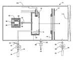
- FIG. 1is a schematic of an indirectly heated cathode ion source, illustrating three optional placements for the etchant material.
- FIG. 2is a schematic of the direct dissociative plasma configuration described herein.
- FIG. 3is a schematic diagram of a 300 amu residual gas analyzer, used to monitor by-products of the residue removal reactions. 1 is the global replacement of vacuum chamber with vacuum chamber needed? We should pick one or the other 2 this is ok for XeF 2 but not for NF 3
- FIG. 4is an RGA trace as a function of time showing the efficacy of XeF 2 in removing boron residue from an aluminum base layer.
- FIG. 5is an RGA trace as a function of time illustrating that XeF 2 does not react with a tungsten layer.
- the present inventionrelates to a method and apparatus for cleaning the ion source region of an ion implantation system used in the fabrication of a microelectronic device. Specifically, the present invention relates to the in situ removal of residue from the vacuum chamber of the ion implanter and components contained therein by contacting the vacuum chamber and/or components with a gas-phase reactive halide composition, e.g., XeF 2 , NF 3 , F 2 , XeF 6 , SF 6 , C 2 F 6 , IF 5 or IF 7 , for sufficient time and under sufficient conditions to at least partially remove the residue from the components, and to do so in such a manner that residue is removed selectively with respect to the materials from which the components of the ion implanter are constructed.
- a gas-phase reactive halide compositione.g., XeF 2 , NF 3 , F 2 , XeF 6 , SF 6 , C 2 F 6 , IF 5 or IF 7
- ion source regionincludes the vacuum chamber, the source arc chamber, the source insulators, the extraction electrodes, the suppression electrodes, the high voltage insulators and the source bushing.
- the reactive halide gasmay for example include a XeF 2 vapor.
- XeF 2will sublime at room temperature, but may be heated using a heating means to increase the rate of sublimation.
- XeF 2is known to be an effective silicon etchant and has been used as a silicon selective etchant in Micro Electro Mechanical System (MEMS) device processing because it is extremely selective to SiO 2 and other dielectric materials.
- MEMSMicro Electro Mechanical System
- XeF 2reacts with silicon according to the following reaction. 2XeF 2 (g)+Si(s) ⁇ 2Xe(g)+SiF 4 (g) (1)
- the silicon/XeF 2 reactioncan occur without activation, i.e., plasma or thermal heating.
- the reactions disclosed hereinmay occur with or without energetic activation.
- the “residue”may comprise, consist essentially of or consist of silicon, boron, phosphorus, germanium or arsenic.
- the method and apparatus taught hereinis used to at least partially remove the residue from the components of the ion implanter, and to do so in such a manner that residue is removed selectively with respect to the materials from which the components of the ion implanter are constructed, e.g., aluminum, tungsten, etc.
- the term “at least partially remove”is defined as the removal of at least about 25%, more preferably at least about 50%, and most preferably at least about 75% of the residue to be removed.
- gas-phase reactive halide compositione.g., a composition including XeF 2
- a stagnant modee.g., a composition including XeF 2
- a continuous modee.g., a continuous mode
- a direct introduction modee.g., a direct introduction mode
- XeF 2 compositionother reactive halide compositions may be used including, but not limited to, XeF 6 , SF 6 , C 2 F 6 , IF 5 or IF 7 . It is further noted that the XeF 2 composition may comprise, consist essentially of or consist of XeF 2 .
- an etchant container with the XeF 2 composition disposed thereinis communicatively attached to the chamber of the ion implanter to be cleaned, wherein the etchant container and the chamber to be cleaned have a valve disposed therebetween.
- the valvemay be manually or remotely opened whereby the XeF 2 vapor is permitted to fill the chamber to be cleaned until a pre-determined pressure is attained.
- the etchant containermay be moderately heated to increase the sublimation rate and/or the sublimation pressure.
- the cleaning apparatusincludes a separate holding chamber of sufficient volume positioned between the etchant container and vacuum chamber.
- the XeF 2may be flowed first into the holding chamber and stored therein until a pre-determined pressure threshold is reached.
- Such holding chamberserves to allow immediate gas flow to the vacuum chamber on demand and to shorten the “waiting-period” associated with sublimation.
- the walls of the holding chambermay be heated to permit higher pressure storage while avoiding condensation of XeF 2 on interior surfaces of the chamber.
- the holding chambermay further comprise flow-regulating devices, such as a mass flow controller, to achieve reproducible delivery of XeF 2 into the vacuum chamber.
- the vacuum chamberis sealed and the XeF 2 permitted to react for sufficient time and under sufficient conditions to at least partially remove the residue from the vacuum chamber and the components contained therein.
- the vacuum chambercan then be evacuated and the cleaning process repeated as needed.
- the evacuated gas mixturemay be further directed to abatement units including, but not limited to, chemical and/or physical adsorption beds, incinerators, wet scrubbers, or a combination thereof.
- the internal pressure, time, and number of repeat cleaningsmay be readily determined by those of ordinary skill in the art.
- the nature and extent of the cleaning of the residuemay be empirically determined while varying the time and/or contacting conditions (such as temperature, pressure, concentration and partial pressure) of the XeF 2 composition to identify the process conditions producing a desired residue removal result.
- the pressure of the XeF 2 composition in the vacuum chambermay be about 0.3 Torr to about 4.0 Torr, preferably about 0.3 Torr to about 0.7 Torr, and the length of cleaning about 1 to about 4 minutes, which may be repeated about two (2) to about ten (10) times.
- the pressure of the XeF 2is about 0.35 Torr and the length of cleaning about 1 minute.
- the pressure in the vacuum chamber during cleaningshould be carefully monitored as the pressure will gradually increase as the cleaning reaction proceeds and should plateau when the reaction has run its course.
- a residual gas analyzermay be used to measure the concentration of XeF 2 and other reaction byproducts, which may also be useful for monitoring the progress of the cleaning process.
- a residual gas analyzer(RGA), as shown schematically in FIG. 3 , may be attached to the vacuum chamber and used to monitor the by-products of the residue removal reactions.
- the RGAmay be a 200 amu or 300 amu analyzer, most preferably a 300 amu analyzer.
- the XeF 2 gasis generated without energetic activation, although activation is contemplated herein.
- effective cleaningcan be performed at room temperature, although cleaning is contemplated at temperature in a range of about 0° C. to about 1000° C. depending on the circumstances.
- the process parametersare chosen to ensure that the reactive halide gas is essentially non-reactive with the ion source region components material of construction.
- “essentially non-reactive”corresponds to less than about 5% of the total reactive halide gas reacts with the components of the ion source region, preferably less than about 2%, most preferably less than about 1%.
- FIG. 1An example of the stagnant mode for cleaning an ion source region 10 is shown in FIG. 1 , which includes a vacuum chamber 100 , an arc chamber 16 , the acceleration electrode 14 , the deceleration electrode 12 , the cathode 18 , the anticathode 20 and the gate valve 102 .
- the etchant container 80 holding the XeF 2may be communicatively connected to the arc chamber 16 by the dedicated vapor feed line 90 (as shown) or alternatively, although not shown in FIG. 1 , the etchant container 80 may be communicatively connected to the vacuum chamber 100 .
- valve 84is manually or automatically opened to permit the XeF 2 to flow from the etchant container 80 to the arc chamber 16 .
- the XeF 2 from an etchant container such as 80may be introduced into the arc chamber via a reactive gas inlet line (e.g., component 22 ) instead of a dedicated XeF 2 inlet line.
- Sublimation of the XeF 2 sourcemay be assisted by heating the etchant container 80 using a heating means including, but not limited to, heater wires 88 , or an oven.
- the entire etchant container housing 82may be water cooled.
- a holding chambermay be situated between the etchant container and the vacuum or arc chamber. Following at least partial removal of the residue from the interior of the chamber to be cleaned, valve 92 is opened and the gases are evacuated using pump 96 via outlet line 94 .
- an etchant container with the XeF 2 composition disposed thereinis directly or indirectly communicatively attached to the vacuum chamber or to the arc chamber, whereby the etchant container and the chambers to be cleaned has at least one valve disposed therebetween.
- An inert carrier gasmay be arranged to flow continuously over the XeF 2 composition in the etchant container to deliver a steady stream of XeF 2 to the chamber to be cleaned.
- the flow rate of the carrier gas, temperature of the etchant container, and cleaning timeare experimental parameters readily determined by those skilled in the art.
- a holding chambermay be situated between the etchant container and the chamber to be cleaned.
- FIG. 1An example of the continuous mode, wherein the etchant container is communicatively connected to the arc chamber, is shown in FIG. 1 .
- the etchant container 40 holding the XeF 2 compositionis communicatively connected to the gas inlet line 22 via the valve 42 .
- Outlet valve 92 , pump 96 and outlet line 94are positioned to withdraw gases from the vacuum chamber 100 .
- inert gas container 44 , valve 46 , valve 42 and valve 92are open, and pump 96 is operating, inert gas flows continuously over the XeF 2 composition in the etchant container 40 and the mixture is introduced into the arc chamber 16 via the gas inlet line 22 .
- the gasesegress out of the chamber via outlet line 94 .
- the XeF 2 /inert gas mixturemay be introduced into the arc chamber via a dedicated XeF 2 vapor feed line (i.e., analogous to component 90 ).
- Inert gases contemplated hereininclude, but are not limited to, argon, nitrogen, xenon, and helium.
- a further alternativeincludes sublimation assistance by heating the etchant container 40 using heating means, as described previously with regards to the stagnant mode.
- FIG. 1illustrates the direct introduction of the XeF 2 composition into the vacuum chamber 100 .
- XeF 2 from etchant container 60is communicatively connected to the vacuum chamber 100 via a dedicated inlet line.
- inert gas container 64When inert gas container 64 , valve 66 , valve 62 and valve 92 are open, and pump 96 is operating, inert gas flows continuously over the XeF 2 composition in the etchant container 60 and the mixture is introduced into the vacuum chamber 100 via the dedicated inlet line.
- an etchant container with pre-measured amounts of XeF 2 compositione.g., in the form of pellets, is introduced into the sealed vacuum chamber 100 .
- the XeF 2completely sublimates in the vacuum chamber and the XeF 2 is permitted to react for sufficient time and under sufficient conditions to at least partially remove the residue from the ion source region components.
- the amount of etchant and the time required for cleaningare readily determined by those skilled in the art. Methods for mechanical dispensing, i.e., etchant containers, are readily engineered by those skilled in the art.
- valve 92is opened and the gases are evacuated using pump 96 via outlet line 94 . Direct introduction cleaning may be repeated as necessary.
- the reactive halide gasmay for example comprise a nitrogen trifluoride (NF 3 ) vapor.
- NF 3is used in the semiconductor industry as a fluorine source for plasma etching, e.g., in situ chamber cleaning of CVD reactors. Additional applications include etching of polysilicon, silicon nitride, tungsten silicide and tungsten films.
- NF 3dissociates into reactive halide species in the plasma, such as fluorine radicals and/or fluoride ions, said reactive halide species subsequently reacting with the residue to be removed. For example, if the residue includes boron, cleaning occurs according to the following reaction. 3F 2 (g)+2B(s) ⁇ 2BF 3 (g) (5)
- a NF 3 source 222is communicatively connected to the arc chamber 210 , with a valve situated therebetween 220 (see FIG. 2 ).
- the NF 3 sourceis communicatively connected with the reactive gas, e.g., BF 3 , inlet tube 218 , allowing introduction of NF 3 simultaneously with other ion source dopant materials.
- the reactive gase.g., BF 3
- inlet tube 218e.g., inlet tube 218
- other means of introducing NF 3 into the arc chamberare contemplated, for example via a dedicated NF 3 inlet line.
- NF 3enters the arc chamber 210 and the fluoride ions are generated using the existing plasma equipment (e.g., the filament 212 , cathode 214 and the anticathode 216 ) or some additional electronic means arranged within the arc chamber 210 .
- Diluent gasesmay be added to the arc chamber to dilute the highly reactive fluoride ions.
- Parameterssuch as NF 3 flow rate into the arc chamber, amount of diluent gas, chamber pressure and time required for cleaning are readily determined by those skilled in the art. Multiple pressures and flow rates are also contemplated, wherein the different pressures and flow rates are used sequentially to effect different plasma shapes and consequently different concentration profiles. Different profiles may be useful for cleaning different areas of the arc chamber, i.e., outer corners, etc.
- the gasesare evacuated via an outlet line and optionally abated.
- Additional cleaning gases contemplated for introduction using the direct dissociative plasma introduction mode, in addition to NF 3include XeF 2 , XeF 6 , IF 5 , IF 7 , SF 6 and C 2 F 6 .
- the reactive halide gasis fluorine, for example as delivered from Advanced Technology Materials VAC cylinder (Danbury, Conn., USA).
- Fluorineis an extremely corrosive gas and can be used with or without thermal or electrical activation. Without activation, the fluorine gas can be admitted directly to the ion source region, wherein the gas is permitted to spontaneously react for sufficient time and under sufficient conditions to at least partially remove the residue. If additional activation is required, components may be heated or left at an elevated temperature and the gas permitted to react for sufficient time to at least partially remove the residue.
- a plasmamay be generated within the arc chamber (as described previously) to further induce fluorine activation.
- the etchant gasmay be blended with the implanting species, e.g., boron trifluoride, so that etching and implanting may occur simultaneously, which is cost effective in terms of minimization of down time and elimination of additional expensive delivery systems.
- implanting speciese.g., boron trifluoride
- the advantages of the present inventioninclude, but are not limited to, selective cleaning of unwanted residue in the ion source region of an ion implantation system, the ability to clean the residue without using plasma-induced radicals thereby minimizing damage to the components of the ion source region, and effective cleaning at room temperature.
- Residue removal from the ion source region using the method introduced hereinreduces source glitching and extraction arcing, thereby contributing to more stable operation of the ion implanter. Further, the ion source lifetime and MTBF are increased, with a concomitant decrease in preventative maintenance costs and time.
- In situ cleaning of the ion source regionshould be performed about 1 to 2 times per week, although the number of cleanings may be more or less often depending on how often the ion implanter is used. Typically, the length of the entire cleaning operation is about 1 hour, although the cleaning time may be more or less.
- the ion sourceis turned off and the source isolation valve is closed prior to introduction of the etchant gas (or the etchant container in the direct introduction mode). Following residue removal, the ion source is restarted and normal ion implanter operations may be resumed.
- off-line (ex situ) cleaning of the components of the ion source region using a vapor phaseis disclosed.
- components from any part of the ion implanter which are delicatee.g., graphite-containing components
- off-line cleanerssuch as harsh abrasives or liquids.
- Off-line cleaning using a vapor phase materialis an advance in the art because abrasives can damage the delicate components and liquids which enter the pores of the delicate components during cleaning must be pumped out of the pores during pump down of the ion source region.
- the ion source or any other power suppliesare turned off, relevant isolation valves are closed, and the ion source or other vacuum chamber is vented to atmospheric pressure.
- the ion source regionis allowed to cool to room temperature before disengagement of the components to be cleaned from the ion source region.
- the componentsare removed from the implanter and positioned in a separate, off-line vacuum chamber with a simple pumping system and valves.
- Etchant gasfor example XeF 2
- the off-line vacuum chamberis a stand alone unit that is able to service numerous ion implanters, e.g., upwards of 10-12, in the fab.
- Test sampleswere prepared using electron beam deposition of aluminum, boron, tungsten and silicon on glass microscope slides. The aluminum was used as a bottom layer barrier on the glass slide. Some samples were capped with a protective silicon layer while others were left uncapped and allowed to oxidize. The test samples were sequentially placed into an ex situ XeF 2 reactor and etched for 16 one-minute pulse-etch cycles at a pressure of 300-400 mTorr at room temperature.
- FIG. 4illustrates the removal, as determined by RGA, of boron from a glass slide having a base layer of 500 nm of aluminum with 500 nm of boron deposited thereon. There was no silicon capping layer therefore the boron could have potentially formed an oxide layer prior to etching.
- the XeF 2 etch processremoved most of the boron in about 4 cycles with a concomitant increase in unreacted XeF 2 , indicating that boron removal was decreasing or had ceased altogether.
- FIG. 4illustrates that the boron layer was readily removed using the XeF 2 system and method taught herein, even if an oxide layer had formed thereon prior to etching.
- FIG. 5illustrates the removal, as determined by RGA, of tungsten from a glass slide having a base layer of 500 nm of aluminum with 150 nm of tungsten deposited thereon. There was no silicon capping layer therefore the tungsten could have potentially formed an oxide layer prior to etching. No tungsten compounds were observed by RGA however, the presence of XeF 2 was significant, indicating that no tungsten removal was occurring.
- FIGS. 4 and 5illustrate that the system and method taught herein selectively removes ion implantation residue, e.g., boron, while being essentially non-reactive with the materials of construction of the ion implanter, e.g., tungsten and aluminum.
Landscapes
- Chemical & Material Sciences (AREA)
- Engineering & Computer Science (AREA)
- Physics & Mathematics (AREA)
- Chemical Kinetics & Catalysis (AREA)
- Mechanical Engineering (AREA)
- Metallurgy (AREA)
- Organic Chemistry (AREA)
- Materials Engineering (AREA)
- Analytical Chemistry (AREA)
- General Chemical & Material Sciences (AREA)
- Public Health (AREA)
- Plasma & Fusion (AREA)
- Epidemiology (AREA)
- Health & Medical Sciences (AREA)
- Nonlinear Science (AREA)
- Crystallography & Structural Chemistry (AREA)
- Manufacturing & Machinery (AREA)
- General Physics & Mathematics (AREA)
- Optics & Photonics (AREA)
- Drying Of Semiconductors (AREA)
- Cleaning Or Drying Semiconductors (AREA)
- Physical Vapour Deposition (AREA)
- Electron Sources, Ion Sources (AREA)
Abstract
Description
- (a) introducing an etchant gas from an etchant container into a vacuum chamber of the semiconductor manufacturing tool;
- (b) terminating introduction of the etchant gas into the vacuum chamber upon attainment of a predetermined pressure in the vacuum chamber; and
- (c) reacting the etchant gas with a residue in the vacuum chamber for a sufficient time to at least partially remove the residue from the interior of the vacuum chamber or at least one component contained therein;
wherein the etchant gas is chosen to react selectively with the residue in the vacuum chamber, while being essentially non-reactive with the interior of the vacuum chamber or the components contained therein.
- (a) introducing an etchant material from an etchant container into a vacuum chamber of the ion source region;
- (b) terminating introduction of the etchant gas into the vacuum chamber upon attainment of a predetermined pressure;
- (c) dissociating the etchant material into a reactive halide species in the vacuum chamber using a plasma means positioned in said vacuum chamber; and
- (d) reacting the reactive halide species with a residue in the vacuum chamber for a sufficient time to at least partially remove the residue from the vacuum chamber.
- (a) an etchant material source having an etchant material disposed therein, wherein the etchant material source is communicatively connected to, and is situated upstream of, the vacuum chamber; and
- (b) a valve between the etchant material source and the vacuum chamber;
- wherein said apparatus is further characterized by comprising at least one of the following components (I) and (II):
- (I) a heating means for the etchant material source; and
- (II) an inert gas source having an inert gas disposed therein, wherein the inert gas source is communicatively connected to, and is situated upstream of, the etchant material source.
- (a) positioning the component in an ex situ vacuum chamber;
- (b) introducing an etchant gas from an etchant container into the ex situ vacuum chamber;
- (c) terminating introduction of the etchant gas into the vacuum chamber upon attainment of a predetermined pressure in the vacuum chamber; and
- (d) reacting the etchant gas with a residue in the vacuum chamber for a sufficient time to at least partially remove the residue from the at least one component contained therein;
- wherein the etchant gas is chosen to react selectively with the residue on the at least one component, while being essentially non-reactive with the interior of the vacuum chamber.
2XeF2(g)+Si(s)→2Xe(g)+SiF4(g) (1)
Importantly, the silicon/XeF2reaction can occur without activation, i.e., plasma or thermal heating.
3XeF2(g)+2B(s)→3Xe(g)+2BF3(g) (2)
The use of XeF2as an etchant for arsenic, phosphorus and germanium has not been reported to the best of our knowledge; however, XeF2may prove to be an effective etchant for these materials as well according to the following reactions (3) and (4).
5XeF2(g)+2As(s)→5Xe(g)+2AsF5(g) (3)
5XeF2(g)+2P(s)→5Xe(g)+2PF5(g) (4)
Similar to the silicon/XeF2reaction, the reactions disclosed herein may occur with or without energetic activation. As used herein, the “residue” may comprise, consist essentially of or consist of silicon, boron, phosphorus, germanium or arsenic.
3F2(g)+2B(s)→2BF3(g) (5)
Claims (39)
Priority Applications (12)
| Application Number | Priority Date | Filing Date | Title |
|---|---|---|---|
| US10/973,673US7819981B2 (en) | 2004-10-26 | 2004-10-26 | Methods for cleaning ion implanter components |
| EP05823352.9AEP1807224A4 (en) | 2004-10-26 | 2005-10-21 | Novel methods for cleaning ion implanter components |
| CNA2005800443901ACN101437629A (en) | 2004-10-26 | 2005-10-21 | Novel methods for cleaning ion implanter components |
| KR1020147016073AKR20140085599A (en) | 2004-10-26 | 2005-10-21 | Novel methods for cleaning ion implanter components |
| KR1020137002724AKR20130019458A (en) | 2004-10-26 | 2005-10-21 | Novel methods for cleaning ion implanter components |
| PCT/US2005/038102WO2006047373A2 (en) | 2004-10-26 | 2005-10-21 | Novel methods for cleaning ion implanter components |
| KR1020077012037AKR20070085495A (en) | 2004-10-26 | 2005-10-21 | New method for cleaning ion implanter components |
| JP2007539016AJP5227025B2 (en) | 2004-10-26 | 2005-10-21 | Novel method for cleaning ion implanter components |
| SG200907013-7ASG156669A1 (en) | 2004-10-26 | 2005-10-21 | Novel methods for cleaning ion implanter components |
| US11/577,852US20090095713A1 (en) | 2004-10-26 | 2005-10-21 | Novel methods for cleaning ion implanter components |
| TW094137265ATWI412620B (en) | 2004-10-26 | 2005-10-25 | Methods and apparatus for cleaning semiconductor manufacturing tool |
| JP2012161702AJP2013055328A (en) | 2004-10-26 | 2012-07-20 | Novel methods for cleaning ion implanter components |
Applications Claiming Priority (1)
| Application Number | Priority Date | Filing Date | Title |
|---|---|---|---|
| US10/973,673US7819981B2 (en) | 2004-10-26 | 2004-10-26 | Methods for cleaning ion implanter components |
Related Child Applications (1)
| Application Number | Title | Priority Date | Filing Date |
|---|---|---|---|
| US11/577,852ContinuationUS20090095713A1 (en) | 2004-10-26 | 2005-10-21 | Novel methods for cleaning ion implanter components |
Publications (2)
| Publication Number | Publication Date |
|---|---|
| US20060086376A1 US20060086376A1 (en) | 2006-04-27 |
| US7819981B2true US7819981B2 (en) | 2010-10-26 |
Family
ID=36205072
Family Applications (2)
| Application Number | Title | Priority Date | Filing Date |
|---|---|---|---|
| US10/973,673Expired - Fee RelatedUS7819981B2 (en) | 2004-10-26 | 2004-10-26 | Methods for cleaning ion implanter components |
| US11/577,852AbandonedUS20090095713A1 (en) | 2004-10-26 | 2005-10-21 | Novel methods for cleaning ion implanter components |
Family Applications After (1)
| Application Number | Title | Priority Date | Filing Date |
|---|---|---|---|
| US11/577,852AbandonedUS20090095713A1 (en) | 2004-10-26 | 2005-10-21 | Novel methods for cleaning ion implanter components |
Country Status (8)
| Country | Link |
|---|---|
| US (2) | US7819981B2 (en) |
| EP (1) | EP1807224A4 (en) |
| JP (2) | JP5227025B2 (en) |
| KR (3) | KR20140085599A (en) |
| CN (1) | CN101437629A (en) |
| SG (1) | SG156669A1 (en) |
| TW (1) | TWI412620B (en) |
| WO (1) | WO2006047373A2 (en) |
Cited By (11)
| Publication number | Priority date | Publication date | Assignee | Title |
|---|---|---|---|---|
| US20080191153A1 (en)* | 2005-03-16 | 2008-08-14 | Advanced Technology Materials, Inc. | System For Delivery Of Reagents From Solid Sources Thereof |
| US20090095713A1 (en)* | 2004-10-26 | 2009-04-16 | Advanced Technology Materials, Inc. | Novel methods for cleaning ion implanter components |
| US20100112795A1 (en)* | 2005-08-30 | 2010-05-06 | Advanced Technology Materials, Inc. | Method of forming ultra-shallow junctions for semiconductor devices |
| US20100154835A1 (en)* | 2006-04-26 | 2010-06-24 | Advanced Technology Materials, Inc. | Cleaning of semiconductor processing systems |
| US20100327159A1 (en)* | 2009-06-26 | 2010-12-30 | Varian Semiconductor Equipment Associates, Inc. | Ion Source Cleaning End Point Detection |
| US20110260621A1 (en)* | 2008-10-17 | 2011-10-27 | Pascal Sortais | Low-power gaseous plasma source |
| US20140199492A1 (en)* | 2013-01-16 | 2014-07-17 | Nissin Ion Equipment Co., Ltd. | Ion implanter and method of operating ion implanter |
| US9960042B2 (en) | 2012-02-14 | 2018-05-01 | Entegris Inc. | Carbon dopant gas and co-flow for implant beam and source life performance improvement |
| US9991095B2 (en) | 2008-02-11 | 2018-06-05 | Entegris, Inc. | Ion source cleaning in semiconductor processing systems |
| US10497569B2 (en) | 2009-07-23 | 2019-12-03 | Entegris, Inc. | Carbon materials for carbon implantation |
| US12112859B2 (en) | 2021-10-01 | 2024-10-08 | Shine Technologies, Llc | Ion production system with fibrous lattice for ion collection |
Families Citing this family (55)
| Publication number | Priority date | Publication date | Assignee | Title |
|---|---|---|---|---|
| US7422983B2 (en)* | 2005-02-24 | 2008-09-09 | International Business Machines Corporation | Ta-TaN selective removal process for integrated device fabrication |
| US20100224264A1 (en) | 2005-06-22 | 2010-09-09 | Advanced Technology Materials, Inc. | Apparatus and process for integrated gas blending |
| US7491947B2 (en)* | 2005-08-17 | 2009-02-17 | Varian Semiconductor Equipment Associates, Inc. | Technique for improving performance and extending lifetime of indirectly heated cathode ion source |
| US7943204B2 (en) | 2005-08-30 | 2011-05-17 | Advanced Technology Materials, Inc. | Boron ion implantation using alternative fluorinated boron precursors, and formation of large boron hydrides for implantation |
| DE102005047081B4 (en)* | 2005-09-30 | 2019-01-31 | Robert Bosch Gmbh | Process for the plasma-free etching of silicon with the etching gas ClF3 or XeF2 |
| DE102005054605B4 (en)* | 2005-11-16 | 2010-09-30 | Bruker Daltonik Gmbh | Automatic cleaning of ion sources |
| US8278222B2 (en)* | 2005-11-22 | 2012-10-02 | Air Products And Chemicals, Inc. | Selective etching and formation of xenon difluoride |
| US20080142039A1 (en)* | 2006-12-13 | 2008-06-19 | Advanced Technology Materials, Inc. | Removal of nitride deposits |
| SG166102A1 (en) | 2007-03-31 | 2010-11-29 | Advanced Tech Materials | Methods for stripping material for wafer reclamation |
| JP5011013B2 (en)* | 2007-07-24 | 2012-08-29 | 大陽日酸株式会社 | Xenon difluoride gas supply device |
| US20090084988A1 (en)* | 2007-09-27 | 2009-04-02 | Varian Semiconductor Equipment Associates, Inc. | Single wafer implanter for silicon-on-insulator wafer fabrication |
| JP2011523764A (en)* | 2008-05-30 | 2011-08-18 | アクセリス テクノロジーズ, インコーポレイテッド | Control of particles in a semiconductor wafer when borohydride is implanted into the semiconductor wafer |
| US7888662B2 (en)* | 2008-06-20 | 2011-02-15 | Varian Semiconductor Equipment Associates, Inc. | Ion source cleaning method and apparatus |
| US8809800B2 (en)* | 2008-08-04 | 2014-08-19 | Varian Semicoductor Equipment Associates, Inc. | Ion source and a method for in-situ cleaning thereof |
| US8263944B2 (en)* | 2008-12-22 | 2012-09-11 | Varian Semiconductor Equipment Associates, Inc. | Directional gas injection for an ion source cathode assembly |
| KR101658975B1 (en)* | 2009-02-11 | 2016-09-23 | 엔테그리스, 아이엔씨. | Ion source cleaning in semiconductor processing systems |
| US8110889B2 (en) | 2009-04-28 | 2012-02-07 | Applied Materials, Inc. | MOCVD single chamber split process for LED manufacturing |
| WO2010129289A2 (en)* | 2009-04-28 | 2010-11-11 | Applied Materials, Inc. | Decontamination of mocvd chamber using nh3 purge after in-situ cleaning |
| US9627180B2 (en)* | 2009-10-01 | 2017-04-18 | Praxair Technology, Inc. | Method for ion source component cleaning |
| FR2951581B1 (en)* | 2009-10-19 | 2011-12-16 | Ecole Polytech | METHOD FOR MANUFACTURING A MULTILAYER FILM COMPRISING AT LEAST ONE ULTRA-THIN LAYER OF CRYSTALLINE SILICON AND DEVICES OBTAINED THEREBY |
| US8598022B2 (en) | 2009-10-27 | 2013-12-03 | Advanced Technology Materials, Inc. | Isotopically-enriched boron-containing compounds, and methods of making and using same |
| SG10201605310RA (en)* | 2009-10-27 | 2016-08-30 | Entegris Inc | Ion implantation system and method |
| US20110108058A1 (en)* | 2009-11-11 | 2011-05-12 | Axcelis Technologies, Inc. | Method and apparatus for cleaning residue from an ion source component |
| FR2957454B1 (en)* | 2010-03-09 | 2013-05-17 | Essilor Int | METHOD FOR CONDITIONING AN ION CANNON |
| US9984855B2 (en)* | 2010-11-17 | 2018-05-29 | Axcelis Technologies, Inc. | Implementation of co-gases for germanium and boron ion implants |
| US20130017644A1 (en)* | 2011-02-18 | 2013-01-17 | Air Products And Chemicals, Inc. | Fluorine Based Chamber Clean With Nitrogen Trifluoride Backup |
| JP2012204248A (en)* | 2011-03-28 | 2012-10-22 | Panasonic Corp | Plasma generating device and washing and cleaning device using the same |
| US8822913B2 (en) | 2011-12-06 | 2014-09-02 | Fei Company | Inductively-coupled plasma ion source for use with a focused ion beam column with selectable ions |
| US9093372B2 (en) | 2012-03-30 | 2015-07-28 | Varian Semiconductor Equipment Associates, Inc. | Technique for processing a substrate |
| US9062377B2 (en)* | 2012-10-05 | 2015-06-23 | Varian Semiconductor Equipment Associates, Inc. | Reducing glitching in an ion implanter |
| CN103785647A (en)* | 2012-10-26 | 2014-05-14 | 上海华虹宏力半导体制造有限公司 | Method for improving service life of parts through ion chamber automatic cleaning through ion injection device |
| JP5950855B2 (en)* | 2013-03-19 | 2016-07-13 | 住友重機械イオンテクノロジー株式会社 | Ion implantation apparatus and cleaning method of ion implantation apparatus |
| US9006690B2 (en)* | 2013-05-03 | 2015-04-14 | Axcelis Technologies, Inc. | Extraction electrode assembly voltage modulation in an ion implantation system |
| JP6201496B2 (en)* | 2013-08-02 | 2017-09-27 | セントラル硝子株式会社 | IF7-derived iodine fluoride compound recovery method and recovery device |
| US10269537B2 (en) | 2013-12-16 | 2019-04-23 | Varian Semiconductor Equipment Associates, Inc. | Vacuum assembly for an ion implanter system |
| KR102111914B1 (en)* | 2014-03-06 | 2020-05-18 | 어플라이드 머티어리얼스, 인코포레이티드 | Plasma abatement of compounds containing heavy atoms |
| US9878901B2 (en)* | 2014-04-04 | 2018-01-30 | Analog Devices, Inc. | Fabrication of tungsten MEMS structures |
| US9330874B2 (en)* | 2014-08-11 | 2016-05-03 | Innovative Micro Technology | Solder bump sealing method and device |
| DE112014006989B4 (en) | 2014-09-25 | 2022-12-22 | Mitsubishi Electric Corporation | ion implanter |
| US10522330B2 (en)* | 2015-06-12 | 2019-12-31 | Varian Semiconductor Equipment Associates, Inc. | In-situ plasma cleaning of process chamber components |
| CN106298421A (en)* | 2015-06-23 | 2017-01-04 | 应用材料公司 | In order to the method and apparatus eliminating the spontaneous combustion by-product from ion implantation technology |
| US10062548B2 (en)* | 2015-08-31 | 2018-08-28 | Varian Semiconductor Equipment Associates, Inc. | Gas injection system for ion beam device |
| WO2017189194A1 (en)* | 2016-04-26 | 2017-11-02 | Applied Materials, Inc. | Temperature controlled remote plasma clean for exhaust deposit removal |
| CN109196617B (en)* | 2016-05-13 | 2021-02-12 | 恩特格里斯公司 | Fluorinated compositions for improving ion source performance in nitrogen ion implantation |
| CN107424895B (en)* | 2016-05-24 | 2021-04-09 | 北京北方华创微电子装备有限公司 | Front-end processing device of semiconductor equipment |
| US10730082B2 (en)* | 2016-10-26 | 2020-08-04 | Varian Semiconductor Equipment Associates, Inc. | Apparatus and method for differential in situ cleaning |
| US10161034B2 (en) | 2017-04-21 | 2018-12-25 | Lam Research Corporation | Rapid chamber clean using concurrent in-situ and remote plasma sources |
| CN110496825B (en)* | 2019-08-22 | 2021-04-13 | 上海华力集成电路制造有限公司 | Device and method for removing vacuum cavity pollution particles |
| JP7385809B2 (en)* | 2019-09-05 | 2023-11-24 | 日新イオン機器株式会社 | How to clean ion beam irradiation equipment |
| EP3815801B1 (en)* | 2019-10-30 | 2025-06-25 | Bond Pulse GmbH | Method for cleaning a surface and vacuum connection method, and retrofitting set for a surface cleaning device, surface cleaning device, and vacuum connecting device comprising a surface cleaning device |
| US10957509B1 (en)* | 2019-11-07 | 2021-03-23 | Applied Materials, Inc. | Insertable target holder for improved stability and performance for solid dopant materials |
| KR20210137395A (en)* | 2020-05-07 | 2021-11-17 | 에이에스엠 아이피 홀딩 비.브이. | Apparatus and methods for performing an in-situ etch of reaction chambers with fluorine-based radicals |
| US11881376B2 (en)* | 2020-10-02 | 2024-01-23 | Entegris, Inc. | Method and systems useful for producing aluminum ions |
| CN113984275B (en)* | 2021-12-24 | 2022-05-10 | 北京凯世通半导体有限公司 | Method for monitoring ultralow temperature ion implantation equipment by measuring vacuum degree |
| US20250253125A1 (en)* | 2024-02-07 | 2025-08-07 | Axcelis Technologies, Inc. | System and method for managing solid phase precursors for an ion implantation system |
Citations (80)
| Publication number | Priority date | Publication date | Assignee | Title |
|---|---|---|---|---|
| US5144147A (en) | 1990-08-31 | 1992-09-01 | Kabushiki Kaisha Toshiba | Ion implantation apparatus and method of cleaning the same |
| US5370568A (en) | 1993-03-12 | 1994-12-06 | Harris Corporation | Curing of a tungsten filament in an ion implanter |
| US5413670A (en) | 1993-07-08 | 1995-05-09 | Air Products And Chemicals, Inc. | Method for plasma etching or cleaning with diluted NF3 |
| US5421957A (en) | 1993-07-30 | 1995-06-06 | Applied Materials, Inc. | Low temperature etching in cold-wall CVD systems |
| JPH0855804A (en) | 1994-08-10 | 1996-02-27 | Toshiba Corp | Method for manufacturing semiconductor thin film |
| US5554845A (en) | 1994-11-14 | 1996-09-10 | Santa Barbara Research Center | Method and apparatus to effectively eliminate optical interference structure in detector response |
| US5554854A (en) | 1995-07-17 | 1996-09-10 | Eaton Corporation | In situ removal of contaminants from the interior surfaces of an ion beam implanter |
| US5565038A (en)* | 1991-05-16 | 1996-10-15 | Intel Corporation | Interhalogen cleaning of process equipment |
| US5620526A (en) | 1993-09-10 | 1997-04-15 | Fujitsu Limited | In-situ cleaning of plasma treatment chamber |
| US5633506A (en) | 1995-07-17 | 1997-05-27 | Eaton Corporation | Method and apparatus for in situ removal of contaminants from ion beam neutralization and implantation apparatuses |
| US5767021A (en) | 1992-06-22 | 1998-06-16 | Matsushita Electric Industrial Co., Ltd. | Dry etching method, chemical vapor deposition method, and apparatus for processing semiconductor substrate |
| US5940724A (en) | 1997-04-30 | 1999-08-17 | International Business Machines Corporation | Method for extended ion implanter source lifetime |
| US5943594A (en) | 1997-04-30 | 1999-08-24 | International Business Machines Corporation | Method for extended ion implanter source lifetime with control mechanism |
| EP0945892A2 (en) | 1998-03-27 | 1999-09-29 | Eaton Corporation | System and method for in-process cleaning of an ion source |
| US5977552A (en) | 1995-11-24 | 1999-11-02 | Applied Materials, Inc. | Boron ion sources for ion implantation apparatus |
| US5988187A (en) | 1996-07-09 | 1999-11-23 | Lam Research Corporation | Chemical vapor deposition system with a plasma chamber having separate process gas and cleaning gas injection ports |
| US6033973A (en)* | 1994-12-06 | 2000-03-07 | Semiconductor Energy Laboratory Co., Ltd. | Ion doping device and method of cleaning ion doping system |
| JP2000222724A (en) | 1999-02-02 | 2000-08-11 | Mitsubishi Chemicals Corp | Film forming method and magnetic recording medium manufacturing method |
| US6143191A (en) | 1997-11-10 | 2000-11-07 | Advanced Technology Materials, Inc. | Method for etch fabrication of iridium-based electrode structures |
| US6221169B1 (en) | 1999-05-10 | 2001-04-24 | Axcelis Technologies, Inc. | System and method for cleaning contaminated surfaces in an ion implanter |
| US6224785B1 (en) | 1997-08-29 | 2001-05-01 | Advanced Technology Materials, Inc. | Aqueous ammonium fluoride and amine containing compositions for cleaning inorganic residues on semiconductor substrates |
| US6254792B1 (en) | 1997-11-10 | 2001-07-03 | Advanced Technology Materials, Inc. | Isotropic dry cleaning process for noble metal integrated circuit structures |
| US6259105B1 (en)* | 1999-05-10 | 2001-07-10 | Axcelis Technologies, Inc. | System and method for cleaning silicon-coated surfaces in an ion implanter |
| US6267909B1 (en) | 1997-04-02 | 2001-07-31 | Advanced Technology & Materials Inc. | Planarization composition for removing metal films |
| US6290864B1 (en)* | 1999-10-26 | 2001-09-18 | Reflectivity, Inc. | Fluoride gas etching of silicon with improved selectivity |
| US6306807B1 (en) | 1998-05-18 | 2001-10-23 | Advanced Technology Materials, Inc. | Boric acid containing compositions for stripping residues from semiconductor substrates |
| US6322756B1 (en) | 1996-12-31 | 2001-11-27 | Advanced Technology And Materials, Inc. | Effluent gas stream treatment system having utility for oxidation treatment of semiconductor manufacturing effluent gases |
| US6322600B1 (en) | 1997-04-23 | 2001-11-27 | Advanced Technology Materials, Inc. | Planarization compositions and methods for removing interlayer dielectric films |
| US6344432B1 (en) | 1999-08-20 | 2002-02-05 | Advanced Technology Materials, Inc. | Formulations including a 1,3-dicarbonyl compound chelating agent and copper corrosion inhibiting agents for stripping residues from semiconductor substrates containing copper structures |
| US6355933B1 (en) | 1999-01-13 | 2002-03-12 | Advanced Micro Devices, Inc. | Ion source and method for using same |
| US20020033229A1 (en)* | 2000-09-19 | 2002-03-21 | Lebouitz Kyle S. | Apparatus for etching semiconductor samples and a source for providing a gas by sublimination thereto |
| US6379575B1 (en) | 1997-10-21 | 2002-04-30 | Applied Materials, Inc. | Treatment of etching chambers using activated cleaning gas |
| WO2002050883A1 (en)* | 2000-12-18 | 2002-06-27 | Sumitomo Precision Products Co., Ltd | Cleaning method and etching method |
| US20020083961A1 (en)* | 2000-10-04 | 2002-07-04 | Toshihito Tsuga | Method and apparatus for cleaning semiconductor wafer |
| US6559462B1 (en) | 2000-10-31 | 2003-05-06 | International Business Machines Corporation | Method to reduce downtime while implanting GeF4 |
| US6566315B2 (en) | 2000-12-08 | 2003-05-20 | Advanced Technology Materials, Inc. | Formulations including a 1,3-dicarbonyl compound chelating agent and copper corrosion inhibiting agents for stripping residues from semiconductor substrates containing copper structures |
| US20030098038A1 (en) | 2001-11-26 | 2003-05-29 | Siegele Stephen H. | System and method for on-site generation and distribution of fluorine for fabrication processes |
| US6620258B1 (en) | 1999-05-21 | 2003-09-16 | Kojair Tech Oy | Method for washing instruments used in semiconductor industry |
| US6620256B1 (en)* | 1998-04-28 | 2003-09-16 | Advanced Technology Materials, Inc. | Non-plasma in-situ cleaning of processing chambers using static flow methods |
| US20030183244A1 (en) | 2002-04-02 | 2003-10-02 | Applied Materials, Inc. | Method of cleaning a semiconductor processing chamber |
| US20040006249A1 (en) | 2002-07-08 | 2004-01-08 | Showa Denko K.K., Nikon Corporation | Fluorination treatment apparatus, process for producing fluorination treated substance, and fluorination treated substance |
| US6699399B1 (en) | 1997-11-12 | 2004-03-02 | Applied Materials, Inc | Self-cleaning etch process |
| US6756600B2 (en) | 1999-02-19 | 2004-06-29 | Advanced Micro Devices, Inc. | Ion implantation with improved ion source life expectancy |
| US6767836B2 (en) | 2002-09-04 | 2004-07-27 | Asm Japan K.K. | Method of cleaning a CVD reaction chamber using an active oxygen species |
| US6812648B2 (en) | 2002-10-21 | 2004-11-02 | Guardian Industries Corp. | Method of cleaning ion source, and corresponding apparatus/system |
| US6841141B2 (en) | 2002-09-26 | 2005-01-11 | Advanced Technology Materials, Inc. | System for in-situ generation of fluorine radicals and/or fluorine-containing interhalogen (XFn) compounds for use in cleaning semiconductor processing chambers |
| US6843258B2 (en) | 2000-12-19 | 2005-01-18 | Applied Materials, Inc. | On-site cleaning gas generation for process chamber cleaning |
| US6846424B2 (en) | 1997-11-10 | 2005-01-25 | Advanced Technology Materials, Inc. | Plasma-assisted dry etching of noble metal-based materials |
| US20050016838A1 (en) | 2003-06-06 | 2005-01-27 | Hirohiko Murata | Ion source apparatus and cleaning optimized method thereof |
| US6851432B2 (en) | 2001-04-19 | 2005-02-08 | Advanced Technology Materials, Inc. | Cleaning compositions |
| US6880561B2 (en) | 2000-03-27 | 2005-04-19 | Applied Materials, Inc. | Fluorine process for cleaning semiconductor process chamber |
| US6902629B2 (en) | 2002-04-12 | 2005-06-07 | Applied Materials, Inc. | Method for cleaning a process chamber |
| WO2005059942A2 (en) | 2003-12-12 | 2005-06-30 | Semequip, Inc. | Method and apparatus for extending equipment uptime in ion implantation |
| US6921062B2 (en) | 2002-07-23 | 2005-07-26 | Advanced Technology Materials, Inc. | Vaporizer delivery ampoule |
| WO2005072252A2 (en) | 2004-01-22 | 2005-08-11 | Semequip Inc. | Isotopically-enriched boranes and methods of preparing them |
| GB2412488A (en) | 2004-03-26 | 2005-09-28 | Applied Materials Inc | Ion sources |
| US20050252529A1 (en) | 2004-05-12 | 2005-11-17 | Ridgeway Robert G | Low temperature CVD chamber cleaning using dilute NF3 |
| US20050260354A1 (en) | 2004-05-20 | 2005-11-24 | Varian Semiconductor Equipment Associates, Inc. | In-situ process chamber preparation methods for plasma ion implantation systems |
| US20060005856A1 (en) | 2004-06-29 | 2006-01-12 | Applied Materials, Inc. | Reduction of reactive gas attack on substrate heater |
| US20060019039A1 (en) | 2004-07-20 | 2006-01-26 | Applied Materials, Inc. | Plasma immersion ion implantation reactor having multiple ion shower grids |
| US20060086376A1 (en) | 2004-10-26 | 2006-04-27 | Dimeo Frank Jr | Novel methods for cleaning ion implanter components |
| US7037813B2 (en) | 2000-08-11 | 2006-05-02 | Applied Materials, Inc. | Plasma immersion ion implantation process using a capacitively coupled plasma source having low dissociation and low minimum plasma voltage |
| US7037376B2 (en) | 2003-04-11 | 2006-05-02 | Applied Materials Inc. | Backflush chamber clean |
| US7080545B2 (en) | 2002-10-17 | 2006-07-25 | Advanced Technology Materials, Inc. | Apparatus and process for sensing fluoro species in semiconductor processing systems |
| US20060169915A1 (en) | 2004-11-12 | 2006-08-03 | Varian Semiconductor Equipment Associates, Inc. | Ion source configuration for production of ionized clusters, ionized molecules and ionized mono-atoms |
| US20060272776A1 (en) | 2003-12-12 | 2006-12-07 | Horsky Thomas N | Method and apparatus for extracting ions from an ion source for use in ion implantation |
| US7168436B2 (en) | 1997-12-18 | 2007-01-30 | Central Glass Company, Limited | Gas for removing deposit and removal method using same |
| US7201807B2 (en) | 2002-12-26 | 2007-04-10 | Samsung Electronics Co., Ltd. | Method for cleaning a deposition chamber and deposition apparatus for performing in situ cleaning |
| US7201174B2 (en) | 2000-08-08 | 2007-04-10 | Tokyo Electron Limited | Processing apparatus and cleaning method |
| US20070117396A1 (en) | 2005-11-22 | 2007-05-24 | Dingjun Wu | Selective etching of titanium nitride with xenon difluoride |
| US7228724B2 (en) | 2002-10-17 | 2007-06-12 | Advanced Technology Materials, Inc. | Apparatus and process for sensing target gas species in semiconductor processing systems |
| US7288491B2 (en) | 2000-08-11 | 2007-10-30 | Applied Materials, Inc. | Plasma immersion ion implantation process |
| US20070259111A1 (en) | 2006-05-05 | 2007-11-08 | Singh Kaushal K | Method and apparatus for photo-excitation of chemicals for atomic layer deposition of dielectric film |
| US7296458B2 (en) | 2002-10-17 | 2007-11-20 | Advanced Technology Materials, Inc | Nickel-coated free-standing silicon carbide structure for sensing fluoro or halogen species in semiconductor processing systems, and processes of making and using same |
| US7300038B2 (en) | 2002-07-23 | 2007-11-27 | Advanced Technology Materials, Inc. | Method and apparatus to help promote contact of gas with vaporized material |
| US20080142039A1 (en) | 2006-12-13 | 2008-06-19 | Advanced Technology Materials, Inc. | Removal of nitride deposits |
| US20080191153A1 (en) | 2005-03-16 | 2008-08-14 | Advanced Technology Materials, Inc. | System For Delivery Of Reagents From Solid Sources Thereof |
| US20080223409A1 (en) | 2003-12-12 | 2008-09-18 | Horsky Thomas N | Method and apparatus for extending equipment uptime in ion implantation |
| WO2009102762A2 (en) | 2008-02-11 | 2009-08-20 | Sweeney Joseph D | Ion source cleaning in semiconductor processing systems |
| US20100022095A1 (en) | 2005-11-22 | 2010-01-28 | Air Products And Chemicals, Inc. | Selective Etching and Formation of Xenon Difluoride |
Family Cites Families (40)
| Publication number | Priority date | Publication date | Assignee | Title |
|---|---|---|---|---|
| US3625749A (en)* | 1966-04-06 | 1971-12-07 | Matsushita Electronics Corp | Method for deposition of silicon dioxide films |
| US3602778A (en)* | 1967-09-25 | 1971-08-31 | Hitachi Ltd | Zener diode and method of making the same |
| JPS4820106B1 (en)* | 1968-03-08 | 1973-06-19 | ||
| US3658586A (en)* | 1969-04-11 | 1972-04-25 | Rca Corp | Epitaxial silicon on hydrogen magnesium aluminate spinel single crystals |
| US3725749A (en)* | 1971-06-30 | 1973-04-03 | Monsanto Co | GaAS{11 {11 {11 P{11 {11 ELECTROLUMINESCENT DEVICE DOPED WITH ISOELECTRONIC IMPURITIES |
| JPS5183473A (en)* | 1975-01-20 | 1976-07-22 | Hitachi Ltd | Fujunbutsuno doopinguhoho |
| US4128733A (en)* | 1977-12-27 | 1978-12-05 | Hughes Aircraft Company | Multijunction gallium aluminum arsenide-gallium arsenide-germanium solar cell and process for fabricating same |
| US4600801A (en)* | 1984-11-02 | 1986-07-15 | Sovonics Solar Systems | Fluorinated, p-doped microcrystalline silicon semiconductor alloy material |
| US4718240A (en)* | 1985-03-01 | 1988-01-12 | Helix Technology Corporation | Cryopump regeneration method and apparatus |
| US4703183A (en)* | 1985-12-05 | 1987-10-27 | Eaton Corporation | Ion implantation chamber purification method and apparatus |
| JP2813762B2 (en)* | 1990-02-23 | 1998-10-22 | 東京エレクトロン株式会社 | Ion implanter |
| US5436180A (en)* | 1994-02-28 | 1995-07-25 | Motorola, Inc. | Method for reducing base resistance in epitaxial-based bipolar transistor |
| US5513499A (en)* | 1994-04-08 | 1996-05-07 | Ebara Technologies Incorporated | Method and apparatus for cryopump regeneration using turbomolecular pump |
| GB9709659D0 (en)* | 1997-05-13 | 1997-07-02 | Surface Tech Sys Ltd | Method and apparatus for etching a workpiece |
| US5851270A (en)* | 1997-05-20 | 1998-12-22 | Advanced Technology Materials, Inc. | Low pressure gas source and dispensing apparatus with enhanced diffusive/extractive means |
| US6534007B1 (en)* | 1997-08-01 | 2003-03-18 | Applied Komatsu Technology, Inc. | Method and apparatus for detecting the endpoint of a chamber cleaning |
| TW352464B (en)* | 1997-09-10 | 1999-02-11 | United Semiconductor Corp | Method for reducing cross contamination in ion implantor |
| JPH11317174A (en)* | 1998-04-30 | 1999-11-16 | Sozo Kagaku:Kk | Cleaning method and cleaning mechanism of ion source insulating flange with gas |
| US6130436A (en)* | 1998-06-02 | 2000-10-10 | Varian Semiconductor Equipment Associates, Inc. | Acceleration and analysis architecture for ion implanter |
| US6346452B1 (en)* | 1999-05-03 | 2002-02-12 | National Semiconductor Corporation | Method for controlling an N-type dopant concentration depth profile in bipolar transistor epitaxial layers |
| JP2000350970A (en)* | 1999-05-10 | 2000-12-19 | Eaton Corp | Method and apparatus for cleaning contaminated surface in ion injector |
| DE10011274A1 (en)* | 2000-03-08 | 2001-09-13 | Wolff Walsrode Ag | Plasma-treated sheet materials |
| TW522445B (en)* | 2000-09-15 | 2003-03-01 | Varian Semiconductor Equipment | Faraday system for ion implanters |
| US6580082B1 (en)* | 2000-09-26 | 2003-06-17 | Axcelis Technologies, Inc. | System and method for delivering cooling gas from atmospheric pressure to a high vacuum through a rotating seal in a batch ion implanter |
| JP2002313776A (en)* | 2001-04-19 | 2002-10-25 | Toshiba Corp | Dry etching method and dry etching apparatus |
| US6529424B2 (en)* | 2001-05-17 | 2003-03-04 | Koninklijke Philips Electronics N.V. | Propagation delay independent SDRAM data capture device and method |
| US6835414B2 (en)* | 2001-07-27 | 2004-12-28 | Unaxis Balzers Aktiengesellschaft | Method for producing coated substrates |
| JP3987312B2 (en)* | 2001-08-31 | 2007-10-10 | 株式会社東芝 | Semiconductor device manufacturing apparatus and manufacturing method, and semiconductor manufacturing apparatus cleaning method |
| US6718126B2 (en)* | 2001-09-14 | 2004-04-06 | Applied Materials, Inc. | Apparatus and method for vaporizing solid precursor for CVD or atomic layer deposition |
| JP3891834B2 (en)* | 2001-12-04 | 2007-03-14 | 大陽日酸株式会社 | Gas supply method and apparatus |
| US6620225B2 (en)* | 2002-01-10 | 2003-09-16 | Advanced Technology Materials, Inc. | Adsorbents for low vapor pressure fluid storage and delivery |
| JP2003272554A (en)* | 2002-03-15 | 2003-09-26 | Seiko Epson Corp | Ion implantation apparatus and operation control method thereof |
| JP2003297280A (en)* | 2002-03-29 | 2003-10-17 | Toshiba Corp | Ion implanter |
| US7186385B2 (en)* | 2002-07-17 | 2007-03-06 | Applied Materials, Inc. | Apparatus for providing gas to a processing chamber |
| US7098143B2 (en)* | 2003-04-25 | 2006-08-29 | Texas Instruments Incorporated | Etching method using an at least semi-solid media |
| US6895766B2 (en)* | 2003-06-27 | 2005-05-24 | Helix Technology Corporation | Fail-safe cryopump safety purge delay |
| US7168438B2 (en)* | 2004-09-07 | 2007-01-30 | Hsi-Lu Hung | Control device for opening and closing automatic umbrella |
| DE102004051635A1 (en)* | 2004-10-23 | 2006-05-18 | Man Roland Druckmaschinen Ag | Method for cutting register setting in a web-fed rotary printing press |
| US20060115590A1 (en)* | 2004-11-29 | 2006-06-01 | Tokyo Electron Limited; International Business Machines Corporation | Method and system for performing in-situ cleaning of a deposition system |
| US7641627B2 (en)* | 2005-02-23 | 2010-01-05 | Camras Carl B | Method and apparatus for reducing intraocular pressure |
- 2004
- 2004-10-26USUS10/973,673patent/US7819981B2/ennot_activeExpired - Fee Related
- 2005
- 2005-10-21SGSG200907013-7Apatent/SG156669A1/enunknown
- 2005-10-21JPJP2007539016Apatent/JP5227025B2/ennot_activeExpired - Fee Related
- 2005-10-21KRKR1020147016073Apatent/KR20140085599A/ennot_activeCeased
- 2005-10-21USUS11/577,852patent/US20090095713A1/ennot_activeAbandoned
- 2005-10-21KRKR1020077012037Apatent/KR20070085495A/ennot_activeCeased
- 2005-10-21EPEP05823352.9Apatent/EP1807224A4/ennot_activeWithdrawn
- 2005-10-21CNCNA2005800443901Apatent/CN101437629A/enactivePending
- 2005-10-21WOPCT/US2005/038102patent/WO2006047373A2/enactiveApplication Filing
- 2005-10-21KRKR1020137002724Apatent/KR20130019458A/ennot_activeCeased
- 2005-10-25TWTW094137265Apatent/TWI412620B/ennot_activeIP Right Cessation
- 2012
- 2012-07-20JPJP2012161702Apatent/JP2013055328A/enactivePending
Patent Citations (96)
| Publication number | Priority date | Publication date | Assignee | Title |
|---|---|---|---|---|
| US5144147A (en) | 1990-08-31 | 1992-09-01 | Kabushiki Kaisha Toshiba | Ion implantation apparatus and method of cleaning the same |
| US5565038A (en)* | 1991-05-16 | 1996-10-15 | Intel Corporation | Interhalogen cleaning of process equipment |
| US5767021A (en) | 1992-06-22 | 1998-06-16 | Matsushita Electric Industrial Co., Ltd. | Dry etching method, chemical vapor deposition method, and apparatus for processing semiconductor substrate |
| US5370568A (en) | 1993-03-12 | 1994-12-06 | Harris Corporation | Curing of a tungsten filament in an ion implanter |
| US5413670A (en) | 1993-07-08 | 1995-05-09 | Air Products And Chemicals, Inc. | Method for plasma etching or cleaning with diluted NF3 |
| US5421957A (en) | 1993-07-30 | 1995-06-06 | Applied Materials, Inc. | Low temperature etching in cold-wall CVD systems |
| US5620526A (en) | 1993-09-10 | 1997-04-15 | Fujitsu Limited | In-situ cleaning of plasma treatment chamber |
| JPH0855804A (en) | 1994-08-10 | 1996-02-27 | Toshiba Corp | Method for manufacturing semiconductor thin film |
| US5554845A (en) | 1994-11-14 | 1996-09-10 | Santa Barbara Research Center | Method and apparatus to effectively eliminate optical interference structure in detector response |
| US6033973A (en)* | 1994-12-06 | 2000-03-07 | Semiconductor Energy Laboratory Co., Ltd. | Ion doping device and method of cleaning ion doping system |
| US5554854A (en) | 1995-07-17 | 1996-09-10 | Eaton Corporation | In situ removal of contaminants from the interior surfaces of an ion beam implanter |
| US5633506A (en) | 1995-07-17 | 1997-05-27 | Eaton Corporation | Method and apparatus for in situ removal of contaminants from ion beam neutralization and implantation apparatuses |
| US5977552A (en) | 1995-11-24 | 1999-11-02 | Applied Materials, Inc. | Boron ion sources for ion implantation apparatus |
| US5988187A (en) | 1996-07-09 | 1999-11-23 | Lam Research Corporation | Chemical vapor deposition system with a plasma chamber having separate process gas and cleaning gas injection ports |
| US6322756B1 (en) | 1996-12-31 | 2001-11-27 | Advanced Technology And Materials, Inc. | Effluent gas stream treatment system having utility for oxidation treatment of semiconductor manufacturing effluent gases |
| US6267909B1 (en) | 1997-04-02 | 2001-07-31 | Advanced Technology & Materials Inc. | Planarization composition for removing metal films |
| US6322600B1 (en) | 1997-04-23 | 2001-11-27 | Advanced Technology Materials, Inc. | Planarization compositions and methods for removing interlayer dielectric films |
| US5940724A (en) | 1997-04-30 | 1999-08-17 | International Business Machines Corporation | Method for extended ion implanter source lifetime |
| US5943594A (en) | 1997-04-30 | 1999-08-24 | International Business Machines Corporation | Method for extended ion implanter source lifetime with control mechanism |
| US6224785B1 (en) | 1997-08-29 | 2001-05-01 | Advanced Technology Materials, Inc. | Aqueous ammonium fluoride and amine containing compositions for cleaning inorganic residues on semiconductor substrates |
| US6379575B1 (en) | 1997-10-21 | 2002-04-30 | Applied Materials, Inc. | Treatment of etching chambers using activated cleaning gas |
| US6846424B2 (en) | 1997-11-10 | 2005-01-25 | Advanced Technology Materials, Inc. | Plasma-assisted dry etching of noble metal-based materials |
| US6254792B1 (en) | 1997-11-10 | 2001-07-03 | Advanced Technology Materials, Inc. | Isotropic dry cleaning process for noble metal integrated circuit structures |
| US6143191A (en) | 1997-11-10 | 2000-11-07 | Advanced Technology Materials, Inc. | Method for etch fabrication of iridium-based electrode structures |
| US6709610B2 (en) | 1997-11-10 | 2004-03-23 | Advanced Technology Materials, Inc. | Isotropic dry cleaning process for noble metal integrated circuit structures |
| US20020011463A1 (en)* | 1997-11-10 | 2002-01-31 | Advanced Technology Materials, Inc. | Isotropic dry cleaning process for noble metal integrated circuit structures |
| US6699399B1 (en) | 1997-11-12 | 2004-03-02 | Applied Materials, Inc | Self-cleaning etch process |
| US7168436B2 (en) | 1997-12-18 | 2007-01-30 | Central Glass Company, Limited | Gas for removing deposit and removal method using same |
| US6135128A (en) | 1998-03-27 | 2000-10-24 | Eaton Corporation | Method for in-process cleaning of an ion source |
| EP0945892A2 (en) | 1998-03-27 | 1999-09-29 | Eaton Corporation | System and method for in-process cleaning of an ion source |
| US6620256B1 (en)* | 1998-04-28 | 2003-09-16 | Advanced Technology Materials, Inc. | Non-plasma in-situ cleaning of processing chambers using static flow methods |
| US6306807B1 (en) | 1998-05-18 | 2001-10-23 | Advanced Technology Materials, Inc. | Boric acid containing compositions for stripping residues from semiconductor substrates |
| US6355933B1 (en) | 1999-01-13 | 2002-03-12 | Advanced Micro Devices, Inc. | Ion source and method for using same |
| JP2000222724A (en) | 1999-02-02 | 2000-08-11 | Mitsubishi Chemicals Corp | Film forming method and magnetic recording medium manufacturing method |
| US6756600B2 (en) | 1999-02-19 | 2004-06-29 | Advanced Micro Devices, Inc. | Ion implantation with improved ion source life expectancy |
| US6221169B1 (en) | 1999-05-10 | 2001-04-24 | Axcelis Technologies, Inc. | System and method for cleaning contaminated surfaces in an ion implanter |
| US6259105B1 (en)* | 1999-05-10 | 2001-07-10 | Axcelis Technologies, Inc. | System and method for cleaning silicon-coated surfaces in an ion implanter |
| US6620258B1 (en) | 1999-05-21 | 2003-09-16 | Kojair Tech Oy | Method for washing instruments used in semiconductor industry |
| US6344432B1 (en) | 1999-08-20 | 2002-02-05 | Advanced Technology Materials, Inc. | Formulations including a 1,3-dicarbonyl compound chelating agent and copper corrosion inhibiting agents for stripping residues from semiconductor substrates containing copper structures |
| US6290864B1 (en)* | 1999-10-26 | 2001-09-18 | Reflectivity, Inc. | Fluoride gas etching of silicon with improved selectivity |
| US6880561B2 (en) | 2000-03-27 | 2005-04-19 | Applied Materials, Inc. | Fluorine process for cleaning semiconductor process chamber |
| US7201174B2 (en) | 2000-08-08 | 2007-04-10 | Tokyo Electron Limited | Processing apparatus and cleaning method |
| US7037813B2 (en) | 2000-08-11 | 2006-05-02 | Applied Materials, Inc. | Plasma immersion ion implantation process using a capacitively coupled plasma source having low dissociation and low minimum plasma voltage |
| US7288491B2 (en) | 2000-08-11 | 2007-10-30 | Applied Materials, Inc. | Plasma immersion ion implantation process |
| US6887337B2 (en) | 2000-09-19 | 2005-05-03 | Xactix, Inc. | Apparatus for etching semiconductor samples and a source for providing a gas by sublimation thereto |
| US20020033229A1 (en)* | 2000-09-19 | 2002-03-21 | Lebouitz Kyle S. | Apparatus for etching semiconductor samples and a source for providing a gas by sublimination thereto |
| US20050230046A1 (en) | 2000-09-19 | 2005-10-20 | Lebouitz Kyle S | Apparatus for etching semiconductor samples and a source for providing a gas by sublimation thereto |
| US20020083961A1 (en)* | 2000-10-04 | 2002-07-04 | Toshihito Tsuga | Method and apparatus for cleaning semiconductor wafer |
| US6559462B1 (en) | 2000-10-31 | 2003-05-06 | International Business Machines Corporation | Method to reduce downtime while implanting GeF4 |
| US6566315B2 (en) | 2000-12-08 | 2003-05-20 | Advanced Technology Materials, Inc. | Formulations including a 1,3-dicarbonyl compound chelating agent and copper corrosion inhibiting agents for stripping residues from semiconductor substrates containing copper structures |
| US20040108296A1 (en)* | 2000-12-18 | 2004-06-10 | Tokiko Kanayama | Cleaning method and etching method |
| WO2002050883A1 (en)* | 2000-12-18 | 2002-06-27 | Sumitomo Precision Products Co., Ltd | Cleaning method and etching method |
| US6843258B2 (en) | 2000-12-19 | 2005-01-18 | Applied Materials, Inc. | On-site cleaning gas generation for process chamber cleaning |
| US6851432B2 (en) | 2001-04-19 | 2005-02-08 | Advanced Technology Materials, Inc. | Cleaning compositions |
| US20030098038A1 (en) | 2001-11-26 | 2003-05-29 | Siegele Stephen H. | System and method for on-site generation and distribution of fluorine for fabrication processes |
| US6843858B2 (en) | 2002-04-02 | 2005-01-18 | Applied Materials, Inc. | Method of cleaning a semiconductor processing chamber |
| US20030183244A1 (en) | 2002-04-02 | 2003-10-02 | Applied Materials, Inc. | Method of cleaning a semiconductor processing chamber |
| US6902629B2 (en) | 2002-04-12 | 2005-06-07 | Applied Materials, Inc. | Method for cleaning a process chamber |
| US20040006249A1 (en) | 2002-07-08 | 2004-01-08 | Showa Denko K.K., Nikon Corporation | Fluorination treatment apparatus, process for producing fluorination treated substance, and fluorination treated substance |
| US7487956B2 (en) | 2002-07-23 | 2009-02-10 | Advanced Technology Materials, Inc. | Method and apparatus to help promote contact of gas with vaporized material |
| US7556244B2 (en) | 2002-07-23 | 2009-07-07 | Advanced Technology Materials, Inc. | Method and apparatus to help promote contact of gas with vaporized material |
| US7300038B2 (en) | 2002-07-23 | 2007-11-27 | Advanced Technology Materials, Inc. | Method and apparatus to help promote contact of gas with vaporized material |
| US6921062B2 (en) | 2002-07-23 | 2005-07-26 | Advanced Technology Materials, Inc. | Vaporizer delivery ampoule |
| US6767836B2 (en) | 2002-09-04 | 2004-07-27 | Asm Japan K.K. | Method of cleaning a CVD reaction chamber using an active oxygen species |
| US6841141B2 (en) | 2002-09-26 | 2005-01-11 | Advanced Technology Materials, Inc. | System for in-situ generation of fluorine radicals and/or fluorine-containing interhalogen (XFn) compounds for use in cleaning semiconductor processing chambers |
| US7296458B2 (en) | 2002-10-17 | 2007-11-20 | Advanced Technology Materials, Inc | Nickel-coated free-standing silicon carbide structure for sensing fluoro or halogen species in semiconductor processing systems, and processes of making and using same |
| US7080545B2 (en) | 2002-10-17 | 2006-07-25 | Advanced Technology Materials, Inc. | Apparatus and process for sensing fluoro species in semiconductor processing systems |
| US7296460B2 (en) | 2002-10-17 | 2007-11-20 | Advanced Technology Materials, Inc. | Apparatus and process for sensing fluoro species in semiconductor processing systems |
| US7228724B2 (en) | 2002-10-17 | 2007-06-12 | Advanced Technology Materials, Inc. | Apparatus and process for sensing target gas species in semiconductor processing systems |
| US6812648B2 (en) | 2002-10-21 | 2004-11-02 | Guardian Industries Corp. | Method of cleaning ion source, and corresponding apparatus/system |
| US7201807B2 (en) | 2002-12-26 | 2007-04-10 | Samsung Electronics Co., Ltd. | Method for cleaning a deposition chamber and deposition apparatus for performing in situ cleaning |
| US7037376B2 (en) | 2003-04-11 | 2006-05-02 | Applied Materials Inc. | Backflush chamber clean |
| US20050016838A1 (en) | 2003-06-06 | 2005-01-27 | Hirohiko Murata | Ion source apparatus and cleaning optimized method thereof |
| US20060272776A1 (en) | 2003-12-12 | 2006-12-07 | Horsky Thomas N | Method and apparatus for extracting ions from an ion source for use in ion implantation |
| US20070210260A1 (en) | 2003-12-12 | 2007-09-13 | Horsky Thomas N | Method And Apparatus For Extending Equipment Uptime In Ion Implantation |
| US20060272775A1 (en) | 2003-12-12 | 2006-12-07 | Horsky Thomas N | Method and apparatus for extracting ions from an ion source for use in ion implantation |
| US20080121811A1 (en) | 2003-12-12 | 2008-05-29 | Horsky Thomas N | Method and apparatus for extending equipment uptime in ion implantation |
| US20070108395A1 (en) | 2003-12-12 | 2007-05-17 | Semequip | Method and apparatus for extracting ions from an ion source for use in ion implantation |
| WO2005059942A2 (en) | 2003-12-12 | 2005-06-30 | Semequip, Inc. | Method and apparatus for extending equipment uptime in ion implantation |
| US20070241689A1 (en) | 2003-12-12 | 2007-10-18 | Horsky Thomas N | Method and apparatus for extending equipment uptime in ion implantation |
| US20080223409A1 (en) | 2003-12-12 | 2008-09-18 | Horsky Thomas N | Method and apparatus for extending equipment uptime in ion implantation |
| WO2005072252A2 (en) | 2004-01-22 | 2005-08-11 | Semequip Inc. | Isotopically-enriched boranes and methods of preparing them |
| GB2412488A (en) | 2004-03-26 | 2005-09-28 | Applied Materials Inc | Ion sources |
| US20050252529A1 (en) | 2004-05-12 | 2005-11-17 | Ridgeway Robert G | Low temperature CVD chamber cleaning using dilute NF3 |
| US20050260354A1 (en) | 2004-05-20 | 2005-11-24 | Varian Semiconductor Equipment Associates, Inc. | In-situ process chamber preparation methods for plasma ion implantation systems |
| US20060005856A1 (en) | 2004-06-29 | 2006-01-12 | Applied Materials, Inc. | Reduction of reactive gas attack on substrate heater |
| US20060019039A1 (en) | 2004-07-20 | 2006-01-26 | Applied Materials, Inc. | Plasma immersion ion implantation reactor having multiple ion shower grids |
| US20090095713A1 (en) | 2004-10-26 | 2009-04-16 | Advanced Technology Materials, Inc. | Novel methods for cleaning ion implanter components |
| US20060086376A1 (en) | 2004-10-26 | 2006-04-27 | Dimeo Frank Jr | Novel methods for cleaning ion implanter components |
| US20060169915A1 (en) | 2004-11-12 | 2006-08-03 | Varian Semiconductor Equipment Associates, Inc. | Ion source configuration for production of ionized clusters, ionized molecules and ionized mono-atoms |
| US20080191153A1 (en) | 2005-03-16 | 2008-08-14 | Advanced Technology Materials, Inc. | System For Delivery Of Reagents From Solid Sources Thereof |
| US20070117396A1 (en) | 2005-11-22 | 2007-05-24 | Dingjun Wu | Selective etching of titanium nitride with xenon difluoride |
| US20100022095A1 (en) | 2005-11-22 | 2010-01-28 | Air Products And Chemicals, Inc. | Selective Etching and Formation of Xenon Difluoride |
| US20070259111A1 (en) | 2006-05-05 | 2007-11-08 | Singh Kaushal K | Method and apparatus for photo-excitation of chemicals for atomic layer deposition of dielectric film |
| US20080142039A1 (en) | 2006-12-13 | 2008-06-19 | Advanced Technology Materials, Inc. | Removal of nitride deposits |
| WO2009102762A2 (en) | 2008-02-11 | 2009-08-20 | Sweeney Joseph D | Ion source cleaning in semiconductor processing systems |
Non-Patent Citations (12)
| Title |
|---|
| Arnó J. et al., "Fluorine Gas: Safe Packaging and Application of a Non-Global Warming Gas for Semiconductor Materials Processing", Micromagazine, 6 pages, (2000). |
| Arnó J. et al., "Safe Fluorine Gas Source for Semiconductor Materials Processing", Electrochemical Society Proceedings, vol. 2001-6, pp. 48-58 (2001). |
| Bartlett, N., Proc. of the Chem. Soc., 218 (1962). |
| Chang, F.I., et al., Proceedings of SPIE, 2641, 117-128 (1995). |
| Chernick, C.L., et al., Science, 138, 136-138 (1962). |
| Co-pending U.S. Appl. No. 12/298,727. |
| Co-pending U.S. Appl. No. 12/358,723. |
| Co-pending U.S. Appl. No. 12/438,502. |
| S.R. Walther, B.O. Pedersen and C.M. McKenn, Ion Sources For Commercial Ion Implanter Applications, 1991, IEEE.* |
| Vugts, M.J.M., et al., J. Vac. Sci. Technol. A, 14(5), 2766-2774 (1996). |
| Williams, K.R., et al., J. Microelectromechanical Systems, 5(4), 256-269 (1996). |
| Winters, H.F., et al., Appl. Phys. Lett., 34(1), 70-73 (1979). |
Cited By (15)
| Publication number | Priority date | Publication date | Assignee | Title |
|---|---|---|---|---|
| US20090095713A1 (en)* | 2004-10-26 | 2009-04-16 | Advanced Technology Materials, Inc. | Novel methods for cleaning ion implanter components |
| US20080191153A1 (en)* | 2005-03-16 | 2008-08-14 | Advanced Technology Materials, Inc. | System For Delivery Of Reagents From Solid Sources Thereof |
| US20100112795A1 (en)* | 2005-08-30 | 2010-05-06 | Advanced Technology Materials, Inc. | Method of forming ultra-shallow junctions for semiconductor devices |
| US20100154835A1 (en)* | 2006-04-26 | 2010-06-24 | Advanced Technology Materials, Inc. | Cleaning of semiconductor processing systems |
| US8603252B2 (en) | 2006-04-26 | 2013-12-10 | Advanced Technology Materials, Inc. | Cleaning of semiconductor processing systems |
| US9991095B2 (en) | 2008-02-11 | 2018-06-05 | Entegris, Inc. | Ion source cleaning in semiconductor processing systems |
| US20110260621A1 (en)* | 2008-10-17 | 2011-10-27 | Pascal Sortais | Low-power gaseous plasma source |
| US8664862B2 (en)* | 2008-10-17 | 2014-03-04 | Centre National De La Recherche Scientifique | Low-power gaseous plasma source |
| US8003959B2 (en)* | 2009-06-26 | 2011-08-23 | Varian Semiconductor Equipment Associates, Inc. | Ion source cleaning end point detection |
| US20100327159A1 (en)* | 2009-06-26 | 2010-12-30 | Varian Semiconductor Equipment Associates, Inc. | Ion Source Cleaning End Point Detection |
| US10497569B2 (en) | 2009-07-23 | 2019-12-03 | Entegris, Inc. | Carbon materials for carbon implantation |
| US9960042B2 (en) | 2012-02-14 | 2018-05-01 | Entegris Inc. | Carbon dopant gas and co-flow for implant beam and source life performance improvement |
| US10354877B2 (en) | 2012-02-14 | 2019-07-16 | Entegris, Inc. | Carbon dopant gas and co-flow for implant beam and source life performance improvement |
| US20140199492A1 (en)* | 2013-01-16 | 2014-07-17 | Nissin Ion Equipment Co., Ltd. | Ion implanter and method of operating ion implanter |
| US12112859B2 (en) | 2021-10-01 | 2024-10-08 | Shine Technologies, Llc | Ion production system with fibrous lattice for ion collection |
Also Published As
| Publication number | Publication date |
|---|---|
| JP2008518482A (en) | 2008-05-29 |
| WO2006047373A3 (en) | 2009-04-23 |
| KR20070085495A (en) | 2007-08-27 |
| US20060086376A1 (en) | 2006-04-27 |
| KR20130019458A (en) | 2013-02-26 |
| TW200624585A (en) | 2006-07-16 |
| JP5227025B2 (en) | 2013-07-03 |
| CN101437629A (en) | 2009-05-20 |
| KR20140085599A (en) | 2014-07-07 |
| JP2013055328A (en) | 2013-03-21 |
| EP1807224A4 (en) | 2014-02-19 |
| WO2006047373A8 (en) | 2006-08-10 |
| EP1807224A2 (en) | 2007-07-18 |
| TWI412620B (en) | 2013-10-21 |
| US20090095713A1 (en) | 2009-04-16 |
| SG156669A1 (en) | 2009-11-26 |
| WO2006047373A2 (en) | 2006-05-04 |
Similar Documents
| Publication | Publication Date | Title |
|---|---|---|
| US7819981B2 (en) | Methods for cleaning ion implanter components | |
| US8603252B2 (en) | Cleaning of semiconductor processing systems | |
| JP5686423B2 (en) | Ion source cleaning and ion implantation system in semiconductor process system | |
| CN102396048B (en) | Ion source cleaning method in semiconductor manufacturing system | |
| CN111263971A (en) | Hydrogen co-generation when aluminum iodide is used as the ion source material |
Legal Events
| Date | Code | Title | Description |
|---|---|---|---|
| AS | Assignment | Owner name:ADVANCED TECHNOLOGY MATERIALS, INC., CONNECTICUT Free format text:ASSIGNMENT OF ASSIGNORS INTEREST;ASSIGNORS:DIMEO, FRANK, JR.;DIETZ, JAMES A.;OLANDER, W. KARL;AND OTHERS;SIGNING DATES FROM 20041021 TO 20050408;REEL/FRAME:016080/0286 Owner name:ADVANCED TECHNOLOGY MATERIALS, INC., CONNECTICUT Free format text:ASSIGNMENT OF ASSIGNORS INTEREST;ASSIGNORS:DIMEO, FRANK, JR.;DIETZ, JAMES A.;OLANDER, W. KARL;AND OTHERS;REEL/FRAME:016080/0286;SIGNING DATES FROM 20041021 TO 20050408 | |
| AS | Assignment | Owner name:ADVANCED TECHNOLOGY MATERIALS, INC., CONNECTICUT Free format text:ASSIGNMENT OF ASSIGNORS INTEREST;ASSIGNOR:ARNO, JOSE I.;REEL/FRAME:018770/0634 Effective date:20060610 | |
| FEPP | Fee payment procedure | Free format text:PAYOR NUMBER ASSIGNED (ORIGINAL EVENT CODE: ASPN); ENTITY STATUS OF PATENT OWNER: LARGE ENTITY | |
| FPAY | Fee payment | Year of fee payment:4 | |
| AS | Assignment | Owner name:GOLDMAN SACHS BANK USA, AS COLLATERAL AGENT, NEW YORK Free format text:SECURITY INTEREST;ASSIGNORS:ENTEGRIS, INC.;POCO GRAPHITE, INC.;ATMI, INC.;AND OTHERS;REEL/FRAME:032815/0852 Effective date:20140430 Owner name:GOLDMAN SACHS BANK USA, AS COLLATERAL AGENT, NEW Y Free format text:SECURITY INTEREST;ASSIGNORS:ENTEGRIS, INC.;POCO GRAPHITE, INC.;ATMI, INC.;AND OTHERS;REEL/FRAME:032815/0852 Effective date:20140430 | |
| AS | Assignment | Owner name:GOLDMAN SACHS BANK USA, AS COLLATERAL AGENT, NEW YORK Free format text:SECURITY INTEREST;ASSIGNORS:ENTEGRIS, INC.;POCO GRAPHITE, INC.;ATMI, INC.;AND OTHERS;REEL/FRAME:032812/0192 Effective date:20140430 Owner name:GOLDMAN SACHS BANK USA, AS COLLATERAL AGENT, NEW Y Free format text:SECURITY INTEREST;ASSIGNORS:ENTEGRIS, INC.;POCO GRAPHITE, INC.;ATMI, INC.;AND OTHERS;REEL/FRAME:032812/0192 Effective date:20140430 | |
| AS | Assignment | Owner name:ENTEGRIS, INC., MASSACHUSETTS Free format text:ASSIGNMENT OF ASSIGNORS INTEREST;ASSIGNOR:ADVANCED TECHNOLOGY MATERIALS, INC.;REEL/FRAME:034894/0025 Effective date:20150204 | |
| FEPP | Fee payment procedure | Free format text:MAINTENANCE FEE REMINDER MAILED (ORIGINAL EVENT CODE: REM.) | |
| AS | Assignment | Owner name:POCO GRAPHITE, INC., MASSACHUSETTS Free format text:RELEASE BY SECURED PARTY;ASSIGNOR:GOLDMAN SACHS BANK USA, AS COLLATERAL AGENT;REEL/FRAME:047477/0032 Effective date:20181106 Owner name:ATMI, INC., CONNECTICUT Free format text:RELEASE BY SECURED PARTY;ASSIGNOR:GOLDMAN SACHS BANK USA, AS COLLATERAL AGENT;REEL/FRAME:047477/0032 Effective date:20181106 Owner name:ENTEGRIS, INC., MASSACHUSETTS Free format text:RELEASE BY SECURED PARTY;ASSIGNOR:GOLDMAN SACHS BANK USA, AS COLLATERAL AGENT;REEL/FRAME:047477/0032 Effective date:20181106 Owner name:ADVANCED TECHNOLOGY MATERIALS, INC., CONNECTICUT Free format text:RELEASE BY SECURED PARTY;ASSIGNOR:GOLDMAN SACHS BANK USA, AS COLLATERAL AGENT;REEL/FRAME:047477/0032 Effective date:20181106 Owner name:ATMI PACKAGING, INC., CONNECTICUT Free format text:RELEASE BY SECURED PARTY;ASSIGNOR:GOLDMAN SACHS BANK USA, AS COLLATERAL AGENT;REEL/FRAME:047477/0032 Effective date:20181106 Owner name:ATMI, INC., CONNECTICUT Free format text:RELEASE BY SECURED PARTY;ASSIGNOR:GOLDMAN SACHS BANK USA, AS COLLATERAL AGENT;REEL/FRAME:047477/0151 Effective date:20181106 Owner name:POCO GRAPHITE, INC., MASSACHUSETTS Free format text:RELEASE BY SECURED PARTY;ASSIGNOR:GOLDMAN SACHS BANK USA, AS COLLATERAL AGENT;REEL/FRAME:047477/0151 Effective date:20181106 Owner name:ATMI PACKAGING, INC., CONNECTICUT Free format text:RELEASE BY SECURED PARTY;ASSIGNOR:GOLDMAN SACHS BANK USA, AS COLLATERAL AGENT;REEL/FRAME:047477/0151 Effective date:20181106 Owner name:ENTEGRIS, INC., MASSACHUSETTS Free format text:RELEASE BY SECURED PARTY;ASSIGNOR:GOLDMAN SACHS BANK USA, AS COLLATERAL AGENT;REEL/FRAME:047477/0151 Effective date:20181106 Owner name:ADVANCED TECHNOLOGY MATERIALS, INC., CONNECTICUT Free format text:RELEASE BY SECURED PARTY;ASSIGNOR:GOLDMAN SACHS BANK USA, AS COLLATERAL AGENT;REEL/FRAME:047477/0151 Effective date:20181106 | |
| LAPS | Lapse for failure to pay maintenance fees | Free format text:PATENT EXPIRED FOR FAILURE TO PAY MAINTENANCE FEES (ORIGINAL EVENT CODE: EXP.); ENTITY STATUS OF PATENT OWNER: LARGE ENTITY | |
| STCH | Information on status: patent discontinuation | Free format text:PATENT EXPIRED DUE TO NONPAYMENT OF MAINTENANCE FEES UNDER 37 CFR 1.362 | |
| FP | Lapsed due to failure to pay maintenance fee | Effective date:20181026 |