US7818653B2 - Methods of soft-input soft-output decoding for nonvolatile memory - Google Patents
Methods of soft-input soft-output decoding for nonvolatile memoryDownload PDFInfo
- Publication number
- US7818653B2 US7818653B2US11/536,286US53628606AUS7818653B2US 7818653 B2US7818653 B2US 7818653B2US 53628606 AUS53628606 AUS 53628606AUS 7818653 B2US7818653 B2US 7818653B2
- Authority
- US
- United States
- Prior art keywords
- likelihood
- data
- bits
- likelihood values
- output
- Prior art date
- Legal status (The legal status is an assumption and is not a legal conclusion. Google has not performed a legal analysis and makes no representation as to the accuracy of the status listed.)
- Active, expires
Links
Images


Classifications
- G—PHYSICS
- G06—COMPUTING OR CALCULATING; COUNTING
- G06F—ELECTRIC DIGITAL DATA PROCESSING
- G06F11/00—Error detection; Error correction; Monitoring
- G06F11/07—Responding to the occurrence of a fault, e.g. fault tolerance
- G06F11/08—Error detection or correction by redundancy in data representation, e.g. by using checking codes
- G06F11/10—Adding special bits or symbols to the coded information, e.g. parity check, casting out 9's or 11's
- G06F11/1008—Adding special bits or symbols to the coded information, e.g. parity check, casting out 9's or 11's in individual solid state devices
- G06F11/1072—Adding special bits or symbols to the coded information, e.g. parity check, casting out 9's or 11's in individual solid state devices in multilevel memories
- H—ELECTRICITY
- H03—ELECTRONIC CIRCUITRY
- H03M—CODING; DECODING; CODE CONVERSION IN GENERAL
- H03M13/00—Coding, decoding or code conversion, for error detection or error correction; Coding theory basic assumptions; Coding bounds; Error probability evaluation methods; Channel models; Simulation or testing of codes
- H03M13/03—Error detection or forward error correction by redundancy in data representation, i.e. code words containing more digits than the source words
- H03M13/05—Error detection or forward error correction by redundancy in data representation, i.e. code words containing more digits than the source words using block codes, i.e. a predetermined number of check bits joined to a predetermined number of information bits
- H03M13/11—Error detection or forward error correction by redundancy in data representation, i.e. code words containing more digits than the source words using block codes, i.e. a predetermined number of check bits joined to a predetermined number of information bits using multiple parity bits
- H03M13/1102—Codes on graphs and decoding on graphs, e.g. low-density parity check [LDPC] codes
- H—ELECTRICITY
- H03—ELECTRONIC CIRCUITRY
- H03M—CODING; DECODING; CODE CONVERSION IN GENERAL
- H03M13/00—Coding, decoding or code conversion, for error detection or error correction; Coding theory basic assumptions; Coding bounds; Error probability evaluation methods; Channel models; Simulation or testing of codes
- H03M13/29—Coding, decoding or code conversion, for error detection or error correction; Coding theory basic assumptions; Coding bounds; Error probability evaluation methods; Channel models; Simulation or testing of codes combining two or more codes or code structures, e.g. product codes, generalised product codes, concatenated codes, inner and outer codes
- H03M13/2906—Coding, decoding or code conversion, for error detection or error correction; Coding theory basic assumptions; Coding bounds; Error probability evaluation methods; Channel models; Simulation or testing of codes combining two or more codes or code structures, e.g. product codes, generalised product codes, concatenated codes, inner and outer codes using block codes
- H—ELECTRICITY
- H03—ELECTRONIC CIRCUITRY
- H03M—CODING; DECODING; CODE CONVERSION IN GENERAL
- H03M13/00—Coding, decoding or code conversion, for error detection or error correction; Coding theory basic assumptions; Coding bounds; Error probability evaluation methods; Channel models; Simulation or testing of codes
- H03M13/29—Coding, decoding or code conversion, for error detection or error correction; Coding theory basic assumptions; Coding bounds; Error probability evaluation methods; Channel models; Simulation or testing of codes combining two or more codes or code structures, e.g. product codes, generalised product codes, concatenated codes, inner and outer codes
- H03M13/2957—Turbo codes and decoding
- H03M13/296—Particular turbo code structure
- H03M13/2963—Turbo-block codes, i.e. turbo codes based on block codes, e.g. turbo decoding of product codes
- H—ELECTRICITY
- H03—ELECTRONIC CIRCUITRY
- H03M—CODING; DECODING; CODE CONVERSION IN GENERAL
- H03M13/00—Coding, decoding or code conversion, for error detection or error correction; Coding theory basic assumptions; Coding bounds; Error probability evaluation methods; Channel models; Simulation or testing of codes
- H03M13/37—Decoding methods or techniques, not specific to the particular type of coding provided for in groups H03M13/03 - H03M13/35
- H03M13/45—Soft decoding, i.e. using symbol reliability information
Definitions
- This inventionrelates to nonvolatile memory systems and to methods of operating nonvolatile memory systems.
- Nonvolatile memory systemsare used in various applications. Some nonvolatile memory systems are embedded in a larger system such as a personal computer. Other nonvolatile memory systems are removably connected to a host system and may be interchanged between different host systems. Examples of such removable memory systems include memory cards and USB flash drives. Electronic circuit cards, including non-volatile memory cards, have been commercially implemented according to a number of well-known standards. Memory cards are used with personal computers, cellular telephones, personal digital assistants (PDAs), digital still cameras, digital movie cameras, portable audio players and other host electronic devices for the storage of large amounts of data.
- PDAspersonal digital assistants
- Such cardsusually contain a re-programmable non-volatile semiconductor memory cell array along with a controller that controls and supports operation of the memory cell array and interfaces with a host to which the card is connected.
- a controllerthat controls and supports operation of the memory cell array and interfaces with a host to which the card is connected.
- Several of the same type of cardmay be interchanged in a host card slot designed to accept that type of card.
- a card made according to one standardis usually not useable with a host designed to operate with a card of another standard.
- Memory card standardsinclude PC Card, CompactFlashTM card (CFTM card), SmartMediaTM card, MultiMediaCard (MMCTM), Secure Digital (SD) card, a miniSDTM card, Subscriber Identity Module (SIM), Memory StickTM, Memory Stick Duo card and microSD/TransFlashTM memory module standards.
- USB flash drive productscommercially available from SanDisk Corporation under its trademark “Cruzer®.” USB flash drives are typically larger and shaped differently than the memory cards described above.
- Data stored in a nonvolatile memory systemmay contain erroneous bits when data is read.
- Traditional ways to reconstruct corrupted datainclude the application of Error Correction Codes (ECCs).
- ECCsError Correction Codes
- Simple Error Correction Codesencode data by storing additional parity bits, which set the parity of groups of bits to a required logical value, when the data is written into the memory system. If during storage the data is erroneous, the parity of groups of bits may change. Upon reading the data from the memory system, the parity of the group of the bits is computed once again by the ECC. Because of the data corruption the computed parity may not match the required parity condition, and the ECC may detect the corruption.
- ECCscan have at least two functions: error detection and error correction. Capability for each of these functions is typically measured in the number of bits can be detected as erroneous and subsequently corrected. Detection capability can be the same or greater than the correction capability. A typical ECC can detect a higher number of error bits than it can correct. A collection of data bits and parity bits is sometimes called a word.
- An early exampleis the (7,4) Hamming code, which has the capability of detecting up to two errors per word (seven bits in this example) and has the capability of correcting one error in such a seven-bit word.
- More sophisticated ECCscan correct more than a single error per word, but it becomes computationally increasingly complex to reconstruct the data.
- Common practiceis to recover the data with some acceptably small likelihood of incorrect recovery.
- the probability of reliable data recoveryalso decreases rapidly or the associated costs in additional hardware and/or performance become prohibitively high.
- datacan be represented by the threshold voltages of transistors.
- different digital data storage valuescorrespond to different voltage ranges. If, for some reason, before or during the read operation the voltage levels shift from their programmed ranges, an error occurs. The error may be detected by the ECC and in some cases these errors may be corrected.
- a nonvolatile memory arrayis connected to a decoder so that encoded data read from the memory array is used to calculate likelihood values associated with bits stored in the memory array.
- a decoderis a Soft-Input Soft-Output (SISO) decoder.
- the encoded datamay be read with a high resolution that gives an indication of likelihood associated with a data bit, not just the logical value of the data bit. For example, where binary data is encoded as +1/ ⁇ 1 volt in a memory, the actual voltage read may be used by the ECC decoder instead of just the sign.
- Likelihood valuesmay be derived from the values read or other sources. Likelihood values may be provided as a soft-input to a SISO decoder.
- the output of the SISO decodermay be converted to a hard-output by a converter. The hard-output represents corrected data.
- a SISO decodermay perform calculations in multiple iterations until some predetermined condition is met.
- a high resolution readmay be achieved by selecting appropriate voltages for individual read steps so that a higher density of reads occurs for a certain portion of a particular threshold voltage function than occurs at another portion. This provides additional resolution for areas of interest, for example, where threshold voltage functions have significant overlap.
- a demodulatormay convert voltages from a memory array into likelihood values Where more than one bit is stored in a cell, a separate likelihood value may be obtained for each bit. Such likelihood values may be used as a soft-input for a SISO decoder.
- FIG. 1shows likelihood functions of threshold voltages of cells programmed to a logic 1 state and a logic 0 state in a nonvolatile memory, including a voltage V D used to discriminate logic 1 and logic 0 states.
- FIG. 2shows components of a memory system including a memory array, modulator/demodulator circuits and encoder/decoder circuits.
- FIG. 3shows likelihood function of read threshold voltages of cells programmed to a logic 1 state and a logic 0 state, showing threshold voltage values.
- FIG. 4shows components of a memory system including a memory array, modulator/demodulator circuits and encoder/decoder circuits, a demodulator providing likelihood values to a decoder.
- FIG. 5shows a NAND string connected to a sense amplifier to read the state of a memory cell.
- FIG. 6Ashows likelihood functions of read threshold voltages of cells programmed to a logic 1 state and a logic 0 state including three threshold voltages.
- FIG. 6Bshows likelihood functions of read threshold voltages of cells programmed to four states and shows threshold voltages where cells are read.
- FIG. 7shows individual likelihood values for both a first and a second bit as a function of threshold voltage in a memory that stores two bits per cell.
- FIG. 8shows an encoder/decoder unit having a Soft-Input Soft-Output (SISO) decoder.
- SISOSoft-Input Soft-Output
- FIG. 9shows an exemplary encoding scheme where the input data is arranged in a square matrix and a parity bit is calculated for each row and column.
- FIG. 10shows a particular example of a signal that is subject to noise causing errors in data that are not correctable using a hard-input decoder but are correctable using a SISO decoder.
- FIG. 11shows an alternative encoding scheme where parity bits are calculated for input data, the input data arranged in rows and columns, a parity bit calculated for each row and column.
- FIG. 12shows components of a memory system including an encoder that provides the encoding shown in FIG. 11 and a demodulator that provides raw likelihood values to a SISO decoder.
- FIG. 13Ashows a first horizontal iteration performed by the SISO decoder of FIG. 12 .
- FIG. 13Bshows a first vertical iteration performed by the SISO decoder of FIG. 12 .
- FIG. 13Cshows a second horizontal iteration performed by the SISO decoder of FIG. 12 .
- FIG. 13Dshows a second vertical iteration performed by the SISO decoder of FIG. 12 .
- FIG. 14shows a Low Density Parity Check (LDPC) parity check matrix used in a SISO decoder.
- LDPCLow Density Parity Check
- FIG. 15shows an encoder/decoder having concatenated encoders and having concatenated decoders.
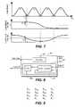
- FIG. 1shows the relationship between a physical parameter indicating a memory cell state (threshold voltage, V T ) and the logical values to which the memory cell may be programmed.
- V Tthreshold voltage
- the cellstores one bit of data.
- Cells programmed to the logic 0 stategenerally have a higher threshold voltage than cells in the logic 1 (unprogrammed) state.
- the logic 1 stateis the unprogrammed state of the memory cell.
- a first likelihood functionis shown for cells programmed to logic 1 and a second for cells programmed to logic 0. However, these functions have some degree of overlap between them.
- a discrimination voltage V Dis used in reading such cells. Cells having a threshold voltage below V D are considered to be in state 1, while those having a threshold voltage above V D are considered to be in state 0. As FIG. 1 shows, this may not always be correct. Because of the overlap between functions, there is a non-zero likelihood that a memory cell programmed to a logic 1 state will be read as having a threshold voltage greater than V D and so will be read as being in a logic 0 state. Similarly, there is a non-zero likelihood that a memory cell programmed to a logic 0 state will be read as having a logic 1 state.
- Overlap between functionsoccurs for a number of reasons including physical defects in the memory array and disturbance caused to programmed cells by later programming or reading operations in the memory array. Overlap may also occur due to a general lack of ability to keep a large number of cells within a very tight threshold voltage range. Certain programming techniques may allow functions of threshold voltages to be narrowed (have smaller standard deviations). However, such programming may take more time. In some memory systems, more than one bit is stored in a memory cell. In general, it is desirable to store as many bits as possible in a memory cell. In order to efficiently use the available threshold voltage range, functions for adjacent states may be such that they significantly overlap.
- Nonvolatile memory systemscommonly employ ECC methods to overcome errors that occur in data that is read from a memory array. Such methods generally calculate some additional ECC bits from input data to be stored in a memory array according to an encoding system. Other ECC schemes may map input data to output data in a more complex way. The ECC bits are stored generally along with the input data or may be stored separately. The input data and ECC bits are later read from the nonvolatile memory array together and a decoder uses both the data and ECC bits to check if any errors are present. In some cases, such ECC bits may also be used to identify a bit that is in error.
- ECC bitsto data bits is not the only way to encode data before storing it in a nonvolatile memory.
- data bitsmay be encoded according to a scheme that provides the following transformations: 00 to 1111, 01 to 1100, 10 to 0011 and 11 to 0000.
- FIG. 2shows an example of input data being stored in a memory system 200 .
- Input datais first received by an ECC unit 201 that includes an encoder 203 .
- the input datamay be host data to be stored in memory system 200 or may be data generated by a memory controller.
- the example of FIG. 2shows four input data bits 1001 .
- Encoder 203then calculates ECC bits (1111) from the input data bits using an encoding scheme.
- One example of an encoding schemeis to generate ECC bits that are parity bits for selected groups of data bits.
- Modulator 207converts the digital data sent by ECC unit 201 to a form in which it is written in a memory array 209 .
- the digital datais converted to a plurality of threshold voltage values in a plurality of memory cells.
- various circuits used to convert digital data to a stored threshold voltage in a memory cellmay be considered to form a modulator.
- each memory cellmay hold one bit of data.
- each memory cellmay have a threshold voltage in one of two ranges, one signifying a logic “1” state and the other signifying a logic “0” state as shown in FIG.
- the memory cells storing a logic “1” statehave a threshold voltage that is less than V D ( ⁇ V D ) while the memory cells storing a logic “0” state have a threshold voltage that is greater than V D (>V D ).
- Cellsmay be programmed and verified to a nominal threshold voltage higher than V D to ensure that, at least initially, there is some preferred separation between cells programmed to the two logic states.
- Datamay be stored in memory array 209 for some period of time. During this time, various events may occur to cause threshold voltages of memory cells to change. In particular, operations involving programming and reading may require voltages to be applied to word lines and bit lines in a manner that affects other previously programmed cells. Such disturbs are particularly common where dimensions of devices are reduced so that the interaction between adjacent cells is significant. Charge may also be lost over long periods of time. Such data retention failures can also cause data to change when read. As a result of such changes, data bits may be read out having different states than the data bits originally programmed. In the example of FIG. 2 , one input data bit 211 is read as having a threshold value less than V D ( ⁇ V D ) when it was originally written having a threshold value greater than V D (>V D ).
- the threshold voltages of memory cellsare converted to bits of data by a demodulator 213 in modulation/demodulation unit 205 .
- Demodulator 213may include sense amplifiers that read a voltage or current from a memory cell in memory array 209 and derive the state of the cell from the reading.
- a memory cell having a threshold voltage less than V Dgives a demodulated output of “1”
- a memory cell having a threshold voltage that is greater than V D (>V D )gives a demodulated output of “0.”
- the second bit 208 of this sequenceis in error as a result of being stored in the memory array 209 .
- Decoder 215determines from data bits and ECC bits if there are any errors. If a small number of errors is present that is within the correction capability of the code, the errors are corrected. If large numbers of errors are present, they may be identified but not corrected if they are within the detection capability of the code. If the number of errors exceeds the detection capability of the code, the errors may not be detected, or may result in an erroneous correction. In the example of FIG. 2 , the error in the second bit is detected and is corrected. This provides an output (1001) from decoder 215 that is identical to the input sequence.
- decoding of memory system 200is considered to be hard-input hard-output decoding because decoder 215 receives only data bits representing input data bits and ECC bits, and decoder 215 outputs a corrected sequence of data bits corresponding to input data bits (or fails to give an output if the number of errors is too high).
- FIG. 4shows a memory system 421 using a data storage process that is similar to that of memory system 200 (using the same input data bits and ECC bits) with a different read process.
- memory system 421instead of simply determining whether a threshold voltage is above or below a particular value, memory system 421 reads threshold voltages as shown in FIG. 3 . It will be understood that actual threshold voltage is not necessarily read. Other means of cell operation may be used to store and retrieve data (e.g. current sensing). Voltage sensing is merely used as an example. Generally, threshold voltage refers to a gate voltage at which a transistor turns on.
- FIG. 4shows a read occurring that provides more detailed information than the previous example. This may be considered a read with a higher resolution than that of FIG.
- the readings corresponding to the second and third bitsare in error.
- the raw voltages read from memory array 423 of FIG. 4 by a series of read operationsare sent to a demodulator 425 in a modulation/demodulation circuit 427 .
- the raw voltageshave a finite resolution dictated by the resolution of the Analog-to-Digital conversion.
- raw datais converted into likelihood data.
- each cell readingis converted into a likelihood that the corresponding bit is a one or a zero.
- the series of readings from the memory array(0.75, 0.05, 0.10, 0.15, 1.25, 1.0, 3.0, and 0.5 volts) can indicate not only the state of the cell, but can also be used to provide a degree of certainty as to that state.
- Thismay be expressed as a likelihood that a memory cell was programmed with a particular bit. Thus, readings that are close to 0 volts may give low likelihood values, while readings that are farther from 0 volts give higher likelihood values.
- the likelihood values shownare log likelihood ratios (explained in detail below). This provides negative numbers for cells in a logic 0 state and positive numbers for cells in a logic 1 state, with the magnitude of the number indicating the likelihood that the state is correctly identified.
- the second and third likelihood values(0.1, 0.2) indicate logic “1”. The second and third values indicate likelihoods that are quite low.
- Likelihood valuesare sent to a decoder 429 in an ECC unit 431 (in some cases, obtaining likelihood values from raw values may be considered as being performed in the decoder).
- the decoder 429performs decoding operations on likelihood values.
- Such a decodermay be considered a soft-input decoder.
- soft-inputrefers to an input that includes some quality information related to data that are to be decoded. The additional information provided as a soft-input generally allows a decoder to obtain better results.
- a decodermay perform decoding calculations using a soft-input to provide calculated likelihood values as an output. This is considered a soft-output and such a decoder is considered a Soft-Input Soft-Output (SISO) decoder.
- SISOSoft-Input Soft-Output
- a SISO decodermay form part of a larger decoder that provides a hard output to another unit. SISO decoders generally provide good performance and in some cases may provide better performance than is possible with hard-input hard-output decoding. In particular, for the same amount of overhead (number of ECC bits) a SISO decoder may provide greater error correction capability.
- a suitable encoding/decoding schememay be implemented and demodulation is adapted to efficiently obtain a soft-input without excessive complexity and without requiring excessive time for reading data from the memory array.
- a soft-input for a SISO decoderis provided by reading data in a nonvolatile memory array with a resolution that resolves a larger number of states than were used in programming the memory.
- datamay be written by programming a memory cell to one of two threshold voltage ranges and subsequently read by resolving three or more threshold voltage ranges.
- the number of threshold voltage ranges used in readingwill be some multiple of the number of threshold voltage ranges used in programming (for example, twice as many). However, this is not always the case.
- An encoder/decoder circuitmay be formed as a dedicated circuit or may this function may be performed by firmware in a controller.
- a controlleris an Application Specific Integrated Circuit (ASIC) that has circuits designed for specific functions such as ECC and also has firmware to manage controller operations.
- ASICApplication Specific Integrated Circuit
- an encoder/decodermay be formed by a combination of hardware and firmware in the memory controller.
- the modulator/demodulator circuitsmay be on a memory chip, on a controller chip, on a separate chip or some combination.
- modulation circuitswill include at least some components on the memory chip (such as peripheral circuits connected to a memory array). While FIG. 4 indicates threshold voltages being read to a high resolution (an analog read), the degree of resolution chosen may depend on a number of factors including the type of nonvolatile memory used.
- FIG. 5shows a string 541 of a NAND flash memory array undergoing a read operation.
- a NAND flash memoryis comprised of strings of memory cells connected in series, isolated by select transistors in groups collectively called blocks, the basic unit of erase.
- the other cells of the stringare turned on hard so that the current flowing through the sting depends on the selected cell.
- Appropriate bias voltagesare placed on the gates of the string select transistors 543 , 545 at either end of string 541 (typically, one end is connected to ground) and one or more voltages are sequentially applied to the word line that extends over the selected cell. For a cell holding one bit of data, only a single voltage may be needed.
- a voltage sequencetypically consists of sequentially increasing voltage steps or a binary search pattern. Each step corresponds to a discrimination voltage.
- a cell storing two bitsrequires four states and a cell storing three bits requires eight states etc.
- a sense amplifier 547 attached to a bit linedetermines when the cell switches on and the word line voltage that first causes such switching indicates the threshold voltage range of the cell.
- the resolution of the read operationdepends on the number of voltage steps provided. For example, a single bit read may require 25 microseconds to complete a sensing operation, while a two bit read for the same memory requires 75 microseconds to complete the three sensing operations to fully resolve four states. More voltage steps provide a higher resolution but this requires more time.
- FIG. 6Ashows as example of a single-bit memory cell that is read with a high resolution that resolves more states than the number of states used in programming the memory.
- the horizontal axisindicates threshold voltage (V T ) and the vertical axis indicates likelihood of a cell having this threshold voltage for a given programmed state.
- V Tthreshold voltage
- a single readwas performed to determine if a cell was programmed into one of two states.
- three readsare performed to determine if the cell is in one of four read threshold voltage ranges, 651 - 654 .
- the cellis programmed to one of two threshold voltage ranges (corresponding to two logic states) and is later read with a resolution that identifies the cell as being in one of four threshold voltage ranges (four read states).
- Voltages V 1 , V 2 , V 3 chosen for performing readsare such that the four threshold voltage ranges 651 - 654 are not equal in size and reads are concentrated near where the two functions (for logic 1 and logic 0) overlap.
- One read(at a discrimination voltage V 2 ) is similar to that of FIG. 1 and indicates which state (0 or 1) the memory cell is in.
- the other two reads(at V 1 and V 3 ) are within the threshold voltage ranges of logic 0 and logic 1 but are not centered in these threshold voltage ranges. Instead, these reads are arranged closer to V 2 .
- the four read threshold voltage ranges 651 - 654give an indication of the likelihood that a particular read bit is correct.
- a reading below V 1has a high likelihood of being correct
- a reading between V 1 and V 2has a lower likelihood of being correct
- a reading between V 2 and V 3has a comparatively low likelihood of being correct
- a reading above V 3has a higher likelihood of being correct. It can be seen that reading with a resolution that resolves a higher number of states than were used in programming allows a read operation to obtain likelihood information regarding the data being read.
- FIG. 6Bshows an example of a two-bit MLC memory cell being read with a high resolution that resolves more states than the number of programmed states.
- FIG. 6Bshows a series of read operations being performed with increasing resolution.
- the threshold voltage of the cellis resolved into one of four states corresponding to a threshold voltage less than V 1 , between V 1 and V 2 , between V 2 and V 3 , and greater than V 3 .
- This first readresolves the same number of states as were used in programming.
- a second read READ 2is performed to give a higher resolution.
- READ 2resolves a programmed state such as “10” into three read states that correspond to a central portion of the threshold voltage function (between V 5 and V 6 ) and two outer portions of the threshold voltage function (one between V 1 and V 5 , the other between V 6 and V 2 ).
- a third read, READ 3is performed to give higher resolution again.
- READ 3resolves the read states of READ 2 so that outer portions are further resolved. In this example, read states corresponding to central portions are not further resolved.
- the read operationsmay be performed in the order READ 1 , then READ 2 , then READ 3 or in any other order. Alternatively, individual read steps may be performed in some other order so that they are combined in a single read operation.
- read stepsmay be performed starting from the lowest threshold voltage and going up sequentially according to threshold voltage.
- the read steps of READ 1 , READ 2 and READ 3are arranged in a pattern having a higher density of read operations for outer portions of the threshold voltage function of a particular programmed state than for a central portion. This provides more information regarding outer portions of threshold voltage functions than central portions of such functions. This is because a cell having a threshold voltage in a central portion of a threshold voltage function for a particular state may be assumed to have a high likelihood of being in that state (close to zero likelihood of being in another state) so that further resolution is not required. Outer portions of a particular function may overlap a neighboring function. More information about such an overlap region (where likelihood values change) is desirable.
- a single read stepmay provide information regarding the programmed level of a memory cell.
- the state of a memory cellis read by measuring the current through the cell under certain biasing conditions.
- a current mirrorcan be used to replicate the current from the cell, the replicated current can then be compared with several reference currents in parallel.
- a high resolution readmay be performed in a single step.
- FIG. 7shows how likelihood values related to individual bits may be derived from threshold voltage information from a cell storing more than one bit of data. In this case, individual likelihood values are assigned to each bit.
- FIG. 7shows a likelihood function for the four states (11, 10, 00, 01) of FIG. 6 .
- FIG. 7also shows a likelihood across all four threshold voltage ranges for the first bit (leftmost bit). Likelihood here is shown as the likelihood that a particular bit is a “1,” likelihood could also be given in terms of likelihood that a bit is a “0.”
- a likelihood level of 0is shown. This is the level at which there is an equal likelihood of a 1 or a 0. Below the 0 level, there is a larger likelihood of a 0.
- FIG. 7shows a likelihood across all four threshold voltage ranges for the second bit (rightmost bit). This likelihood is high at either end of the threshold voltage range and low in the middle. Thus, the likelihood values for the two bits have very different patterns.
- FIG. 7shows a threshold voltage V 1 that gives a first-bit likelihood P 1 and a second bit likelihood P 2 .
- P 1is large because threshold voltage V 1 is not close to a threshold voltage associated with a state having a “0” as the first bit.
- P 2is small because V 1 is close to the threshold voltage range for the “10” state. This indicates that, while this bit is probably a 1, the likelihood is little higher than the likelihood that it is a 0.
- FIG. 7shows that likelihood may be very different for different bits stored in the same cell. Even where a read operation indicates a threshold voltage that is in a region of overlap between threshold voltage ranges of neighboring states and thus has an increased risk of being misread, an individual bit may have a very high likelihood value where the overlap is between two states that both have the individual bit in common.
- a demodulatormay use correlation between threshold voltage and individual bit likelihood values like those shown in FIG. 7 to provide raw likelihood values based on readings from a memory array. Where a read operation identifies a threshold voltage range for a cell, likelihood values for each bit may be associated with each such range. Likelihood values may be derived from a variety of information such as characteristics of memory cell behavior for a given technology or from experience of a given memory device. In some cases, likelihood values may vary at different stages during the lifetime of a device.
- LLRLog Likelihood Ratio
- x) is the likelihood that the bit is a “1” and P(d0
- LLRis a convenient way to express likelihood though other systems may also be used. In order to obtain likelihood information from readings from a memory, some conversion or demodulation is generally performed. One convenient manner of performing such demodulation is to use a lookup table that tabulates the relationship between threshold voltage (or some measured parameter in the memory) and the likelihood values of one or more bits.
- a tablemay have N ⁇ R entries so that a likelihood is given for each bit for each read state.
- a high resolution readmay provide likelihood information regarding data stored in the memory.
- Such raw likelihood datamay be provided to a decoder as a soft-input to the decoder.
- FIG. 8shows soft-input data such as described above being supplied to a decoder system 861 that includes a SISO decoder 863 .
- SISO decodersgenerally accept raw likelihood data and perform ECC calculations on the raw likelihood data to provide calculated likelihood data.
- the calculated likelihood datamay be considered a soft-output.
- such a soft-outputis then provided as an input to the SISO decoder so that a second decoding iteration is performed.
- a SISO decodermay perform successive iterations until at least one predetermined condition is achieved.
- a predetermined conditionmay be that all bits have a likelihood that is greater than a certain minimum value.
- a predetermined conditioncould also be an aggregate of likelihood values such as a mean likelihood value.
- a predetermined conditionmay be convergence of results from one iteration to the next (i.e. keep iterating until there is little improvement from additional iterations).
- a predetermined conditionmay be that a predetermined number of iterations are completed. Combinations of these conditions may also be used.
- Decodingis performed using an encoded pattern in the data that is the result of encoding performed by encoder 865 on the data before it was stored.
- Encoder 865 and decoder system 861are both considered parts of ECC unit 867 , which may be implemented in a memory system such as memory system 421 (ECC unit 867 is an example of a unit that may be used as ECC unit 431 ).
- ECC unit 867is an example of a unit that may be used as ECC unit 431 ).
- Various encoding schemesare possible for use with a SISO decoder.
- Decoder 861also includes a hard-soft converter 864 to convert a soft-output from SISO decoder 865 to a hard output
- FIG. 9shows an exemplary encoding scheme that may be used in a SISO decoder such as SISO decoder 863 .
- Data entries D 11 -D 33are arranged in rows and columns with parity bits calculated for each row and column. For example, P 1 is calculated from the row comprising entries D 11 , D 12 and D 13 . Similarly, P 2 is calculated from the row comprising entries D 21 , D 22 and D 23 . P 4 is calculated from the column D 11 , D 21 and D 23 .
- FIG. 10shows the outcome when the data encoded as shown in FIG. 9 is later decoded in both a hard-input hard-output decoder and in a SISO decoder.
- the two logical states of a binary systemare represented by ⁇ 1 and +1 instead of 0 and 1 respectively. It will be understood that any suitable notation may be used and this notation is simply convenient for this example. For soft numbers, the sign indicates whether the bit is most likely a 0 or a 1 and the magnitude of the number indicates the likelihood that this is the correct value.
- a signal 101is shown as a group of bits that include data bits and parity bits calculated according to the encoding scheme of FIG. 9 .
- the signalis generally the output of an encoder that has suitable circuits to calculate parity bits.
- the signalmay be sent to a modulator which then provides suitable voltages to memory cells to program the memory cells to states to record the signal data.
- Noise 103is shown affecting two data bits in this example.
- Noiseis not limited to data bits and may also affect parity bits.
- Noisemay be the result of some physical characteristic of particular cells or may be the result of disturbs that occur in memory when one cell is affected by operations carried out on other cells in the array.
- noiseis considered additive so that data read from the memory reflects the signal data plus the noise, which then becomes the input data for decoding. But noise may have either positive or negative effects on the read value.
- Input 105is the raw data obtained from a demodulator connected to a memory. For example, where a read operation is performed with a high resolution, input data may be generated in this form so that a bit of either signal or parity data is represented by 0.1 instead of a 1 or a 0. This may be considered a likelihood value with a positive value indicating a 1 and a negative value indicating a 0, the magnitude of the value indicating the likelihood that the indicated state is correct. Input 105 may be considered a soft-input because it includes more than a simple 0 or 1 value.
- input 105is converted to hard input 107 by replacing all positive values by +1 and replacing all negative values by ⁇ 1.
- the most significant bitrepresents the sign and may be used as the means of conversion.
- the hard-input hard-output decodermay attempt to correct the data using this hard input.
- parity calculationsindicate an error in each of the second and third rows and an error in each of the second and third columns. There is no unique solution in this situation because D 22 and D 33 could be in error or alternatively D 32 and D 23 could be in error.
- the hard-input hard-output detectorcannot determine which of these solutions is correct. Therefore, a hard-input hard-output decoder is unable to correct the data in this situation
- soft-input correction data 109is generated for the first row from the input.
- Each entry of soft-input correction data 109is calculated from the sign of the product of the other entries in the same row and the magnitude of the smallest entry in the row (calculation of likelihood values is described in more detail below). This gives an indication of what the other entries in the row indicate the entry should be and may be considered a calculated likelihood or an extrinsic likelihood (as opposed to the intrinsic likelihood of the Input).
- the soft-input correction data 109is then added to Input 105 to obtain the soft-output 111 of the first row-iteration.
- the soft-output 111 of the first row-iterationthus combines the intrinsic and extrinsic likelihood values.
- the soft-outputreflects both intrinsic likelihood information from the raw data and extrinsic likelihood information derived from the other entries in the same row that share the same parity bit. Looking at the sign of the soft-output 113 at this point (converting the soft-output to a hard-output) shows that the data is fully corrected.
- the soft-input soft-output decodingcan correct this data where a hard-input hard-output decoder could not.
- the soft-input soft-output decodercan make this correction in one iteration using only row parity calculations. If correction was not completed, then further calculations could be performed using column parity calculations. If such a first column-iteration did not provide full correction, then a second row-iteration could be performed. Thus, a SISO may continue to work towards a solution where a hard-input decoder stops without finding a solution.
- parity bitsare calculated for both rows and columns of the input data (just two input data entries per row or column in this example).
- parity bitsare calculated to be the sum modulo 2 of the input data bits of the row or column.
- FIG. 12shows the input data being received by an encoder 121 in an ECC unit 123 that calculates the parity bits and appends them to the data.
- an encoder 121in an ECC unit 123 that calculates the parity bits and appends them to the data.
- four bits of parity dataare appended to four bits of input data.
- the input data and parity bitsthus form encoded signal data that is sent to a modulator 125 .
- Modulator 125programs individual memory cells according to the signal data. In this case, two bits are stored in a memory cell of memory array 126 , so the eight bits of signal data are stored in four cells having respective threshold voltage levels V 1 -V 4 . Subsequently the memory cells are read as having threshold voltage ranges V 1 ′-V 4 ′.
- the read threshold voltage rangesare demodulated in a demodulator 127 to provide raw likelihood data (1.5, 1.0, 0.2, 0.3, 2.5, 2.0, 6.0, 1.0). This may be obtained using a lookup table or otherwise. In some cases, providing raw likelihood data is considered as a function within a decoder, but for the present case it is considered as taking place within demodulator 127 . A raw likelihood value is obtained for each bit so that even though bits are stored in the same cell, they may have different raw likelihood values. In the present example, demodulator 127 provides likelihood values as Log Likelihood Ratio values, though likelihood may be expressed in other formats also.
- FIGS. 13A-13Dshow how SISO decoder 129 corrects input data.
- Decoder 129is a particular example of a SISO decoder that may be used in a memory system such as memory system 421 (decoder 129 may be used as decoder 429 )
- FIG. 13Ashows a first horizontal iteration using row parity bits 131 to obtain first calculated likelihood values 133 from row likelihood values 132 .
- LLRsare added to obtain calculated likelihood values 133 .
- the sum of two LLRs in this exampleis given by the product of the signs of the two LLRs and ( ⁇ 1), multiplied by the smaller LLR value.
- ⁇indicates LLR addition. Applying this LLR addition to the entries provides calculated likelihood values shown.
- the calculated likelihood corresponding to entry D 11is 0.1 ⁇ 2.5 ⁇ 0.1
- the calculated likelihood corresponding to entry D 12is 1.5 ⁇ 2.5 ⁇ 1.5.
- Calculated (extrinsic) likelihood values 133are then added to the raw (intrinsic) likelihood values 132 to obtain output likelihood values 135 from the first horizontal iteration. So the output likelihood value corresponding to entry D 11 is the raw likelihood value 1.5 plus the calculated likelihood value ⁇ 0.1, giving 1.4.
- the output likelihood values 135 of the top row (1.4, ⁇ 1.4)indicate relatively high likelihood values indicating that the correct bits are 1 and 0.
- likelihood values 135 on the bottom row ( ⁇ 0.1, 0.1)indicate low likelihood values that the bits are 0 and 1 respectively. These likelihood values indicate the correct input bits. However, such low likelihood values may not be considered good enough to terminate decoding at this point. So, additional iterations may be performed.
- FIG. 13Bshows the output likelihood values 135 from the first horizontal iteration being subjected to a first vertical iteration using column parity bits 137 .
- Calculated likelihood values 139 of the first vertical iterationare calculated in the same manner as before, this time along columns using column parity entries 137 .
- D 11is obtained from the LLR sum of D 12 and P 3 ( ⁇ 0.1 and 6.0, giving 0.1).
- D 12is obtained from the LLR sum of D 11 and P 3 (1.4 and 6.0, giving ⁇ 1.4). In this way, calculated likelihood values 139 are obtained for each entry.
- the calculated (extrinsic) likelihood values 139are added to the input likelihood values 135 (the output likelihood values of the first horizontal iteration) to obtain output likelihood values 141 of the first vertical iteration.
- the output likelihood values 141 obtained from the first vertical iteration(1.5, ⁇ 1.5, ⁇ 1.5, 1.1) may be considered sufficiently good to terminate decoding at this point. However, depending on the predetermined condition required to terminate decoding, more decoding iterations may be performed.
- FIG. 13Cshows a second horizontal iteration being performed.
- the calculated likelihood values 139 from the first vertical iterationare first added to the raw likelihood values 132 to obtain input values 143 .
- the input values 143are then used with row parity entries 131 as before to obtain second horizontal calculated likelihood values 145 .
- the second horizontal likelihood values 145are then added to the input values 132 to obtain the output likelihood values 147 of the second horizontal iteration.
- the output likelihood values 147 of the second horizontal iterationdo not provide an overall improvement in likelihood values from the output of the first vertical iteration.
- FIG. 13Dshows a second vertical iteration being performed.
- the output values 147 from the second horizontal iterationare used as input values for this iteration.
- Column parity entries 137are used with the input values to obtain calculated likelihood values 149 as before.
- Calculated likelihood values 149are then added to the input likelihood values 147 to obtain output likelihood values 151 .
- Output values 151 from the second vertical iterationare shown to be improved compared with output values 141 from the first vertical iteration. Thus, it can be seen that additional iterations may provide additional improvement in the data.
- Iterative decodingmay cycle through iterations until some predetermined condition is met.
- the predetermined conditionmay be that each likelihood value in an output set of likelihood values exceeds some minimum likelihood value.
- the predetermined conditionmay be some parameter derived from more than one likelihood value, such as a mean or average likelihood.
- the predetermined conditionmay simply be that a certain number of iterations are preformed.
- a SISO decoderprovides output likelihood values that are then subject to another operation that indicates whether additional SISO iterations should be performed or not.
- FIGS. 13A-13Dmay be considered an example of a technique known as Turbo decoding.
- Horizontal and vertical parity bitsprovide two alternative encoding schemes that can be separately decoded. Using two such decoding schemes together and using the output from one decoding scheme as the input for the other, turbo coding generally provides high error correction capability.
- Efficient decodingdepends on having a suitable encoding/decoding scheme.
- Various schemesare known for encoding data in a manner that is suitable for subsequent decoding in a SISO decoder.
- Encoding/decoding schemesinclude, but are not limited to, turbo codes, product codes, BCH codes, Reed-Solomon codes, convolutional codes (see U.S. patent application Ser. Nos. 11/383,401 and 11/383,405), Hamming codes, and Low Density Parity Check (LDPC) codes.
- LDPCLow Density Parity Check
- LDPC codesare codes that have a parity check matrix that meets certain requirements, resulting in a sparse parity check matrix. This means that each parity check is performed over a relatively small number of bits.
- An example of a parity check matrix H for an LDPC codeis shown in FIG. 14 .
- the conditions for an LDPC codeare: (1) The number of 1s in each row is the same and the number is small in comparison to the total number of entries in the row. (2) The number of is in each column is the same and the number is small in comparison with the total number of entries in the column. (3) The number of 1s in common between any two columns is not greater than 1 (the number of 1s in common may only be zero or one).
- Irregular LDPC codesallow some deviation in the number of 1s in columns and rows. Looking at H, each row has three 1s, out of a total of seven entries in a row, so that condition (1) is met. Each column has three 1s, out of a total of seven entries in a column, so that condition (2) is met. No two columns have more than one 1 in common, so that condition (3) is met. For example, the first, second and fourth columns all have a 1 as the top entry, but none of these columns has another 1 in common.
- matrix Hdefines an LDPC code. The code consists of all code words that satisfy matrix H. This means that seven different parity check conditions (defined by the seven rows) must be met. Each parity check condition looks at three entries in a word. For example, the first row indicates that the first, second and fourth entries in a word must have a sum modulo two of zero.
- Datamay be encoded according to an LDPC code by calculating certain parity bits to form a codeword.
- a codeword of the parity check matrix Hmay be formed of four data bits and three parity bits calculated from the four data bits. Each parity bit is calculated from a relatively small number of data bits, so encoding may be relatively simple, even where a large number of entries are encoded as a block.
- a suitable LDPC code for memory applicationsuses a word of about 4,000-8,000 bits (1-2 sectors, where a sector is 512 bytes). For example, encoding according to the LDPC code may add approximately 12% to the unencoded data. The number of is in a row of a parity check matrix for such a code may be about 32 out of about 4000, so that even though the word is large, the parity calculations are not excessively long. Thus, parity bits may be relatively easily calculated during encoding and parity may also be relatively easily checked during decoding.
- LDPC codesmay be used with hard-input hard-output decoding or SISO decoding. As shown earlier, SISO decoding can sometimes improve performance over hard-input hard-output decoding.
- Raw likelihood valuesmay be supplied to a SISO decoder as LLRs or in some other form.
- An LDPCcan use a SISO decoder in an iterative manner. An entry is common to several parity groups so that a calculated likelihood value obtained from one group provides improved data for another parity group. Such calculations may be iteratively performed until some predetermined condition is met.
- LDPC decodingmay sometimes provide poor results when the number of errors is very low. Correcting errors below a certain number becomes difficult creating an “error floor.”
- One solution to this problemis to combine LDPC decoding with some other form of decoding.
- a hard-input hard-output decoder using BCH or some similar algebraic codemay be added to an LDPC decoder.
- the LDPC decoderreduces the number of errors to some low level, and then the BCH decoder decodes the remaining errors. Decoders operating in series in this manner are referred to as “concatenated.” Concatenated encoding is also performed before data is stored in the memory array in this case.
- FIG. 15shows an example of concatenated encoding and decoding in an ECC unit 155 that includes an encoding system 157 and a decoding system 159 .
- Datais received by the ECC unit 155 and is first encoded in encoder A where it is encoded according to encoding scheme A. Then, the encoded data is sent to encoder B where it is encoded according to encoding scheme B.
- encoding scheme Ais a BCH encoding scheme that adds parity bits to the input data, increasing the amount of data by approximately 4% in one example.
- Encoding scheme Bis an LDPC encoding scheme that adds additional parity bits to the encoded data from encoder A, adding an additional 12% to the data in this example.
- the doubly encoded datais then send to a modulation/demodulation unit and is programmed to a nonvolatile memory array. Subsequently, the doubly encoded data is read from the memory array and is demodulated to provide a soft-input to decoder B. Decoder B decodes data using encoding scheme B. Similarly, decoder A uses encoding scheme A. Decoder B of this example is a SISO decoder that performs one or more decoding iterations on the doubly encoded data. When some predetermined condition is met, decoder B sends output data to decoder A. The output data from decoder B does not generally include entries for parity bits added by encoder B.
- decoder BThe output of decoder B is a soft-output.
- This soft outputmay be converted to a hard-data in a soft-hard converter 161 that removes likelihood information and converts the data to binary information.
- This hard datais then provided as a hard-input to decoder A which performs hard-input, hard-output decoding.
- the hard-output from the second decoderis then sent out of ECC unit 155 as corrected data.
- the predetermined condition for terminating iterative decoding in decoder Bis that decoder A indicates that the data is good. After an iteration is completed in decoder B, a soft-output may be converted to hard data and provided as a hard-input to decoder A. Decoder A then attempts to decode the data. If decoder A cannot decode the data, then decoder B performs at least one additional iteration. If decoder A can decode the data, then no more iterations are required in decoder B. Thus, in this example, decoder A provides a feedback 163 to decoder B to indicate when the decoder B should terminate.
- FIG. 15deals with concatenation of hard-input hard-output and SISO coding
- Other combinationsmay also be used.
- Two or more SISO decodersmay be used in series and two or more hard-input hard-output decoders may also be used.
- Soft-input in the examples described aboveis obtained by reading data with a higher resolution than was used to program the data.
- other informationmay be used to derive soft-input data. Any quality information provided in addition to a simple 1 or 0 determination regarding a data bit stored in memory may be used to provide a soft-input.
- a countis maintained of the number of times a block has been erased. Physical properties of the memory may change in a predictable manner as erase count increases, making certain errors more likely. An erase count may be used to obtain likelihood data where such a pattern is known. Other factors known to affect programmed data in a predictable way may also be used to obtain likelihood information.
- datamay be read from the memory array with the same resolution used to program it and still be used to provide a soft-input.
- Various sources of likelihood informationmay be combined.
- likelihood information from reading data with a high resolutionmay be combined with likelihood data from another source.
- a soft-inputis not limited to likelihood information obtained directly from reading the memory array.
- nonvolatile memoriesare currently in use and the techniques described here may be applied to any suitable nonvolatile memory systems.
- memory systemsmay include, but are not limited to, memory systems based on ferroelectric storage (FRAM or FeRAM), memory systems based on magnetoresistive storage (MRAM), and memories based on phase change (PRAM or “OUM” for “Ovonic Unified Memory”).
Landscapes
- Engineering & Computer Science (AREA)
- Theoretical Computer Science (AREA)
- Quality & Reliability (AREA)
- Physics & Mathematics (AREA)
- General Engineering & Computer Science (AREA)
- General Physics & Mathematics (AREA)
- Read Only Memory (AREA)
- Error Detection And Correction (AREA)
Abstract
Description
where P(d=1|x) is the likelihood that the bit is a “1” and P(d=0|x) is the likelihood that the bit is a “0.” LLR is a convenient way to express likelihood though other systems may also be used. In order to obtain likelihood information from readings from a memory, some conversion or demodulation is generally performed. One convenient manner of performing such demodulation is to use a lookup table that tabulates the relationship between threshold voltage (or some measured parameter in the memory) and the likelihood values of one or more bits. Where the resolution of the read operation divides the threshold voltage range of a memory cell into N read states and the cell stores R bits, a table may have N×R entries so that a likelihood is given for each bit for each read state. In this way, a high resolution read may provide likelihood information regarding data stored in the memory. Such raw likelihood data may be provided to a decoder as a soft-input to the decoder.
LLR(D1)⊕LLR(D2)≈(−1)×sgn[LLR(D1)]×sgn[LLR(D2)]×min[LLR(D1),LLR(D2)]
Where ⊕ indicates LLR addition. Applying this LLR addition to the entries provides calculated likelihood values shown. For example, the calculated likelihood corresponding to entry D11is 0.1⊕2.5≈−0.1, the calculated likelihood corresponding to entry D12is 1.5⊕2.5≈−1.5. Calculated (extrinsic) likelihood values133 are then added to the raw (intrinsic) likelihood values132 to obtain output likelihood values135 from the first horizontal iteration. So the output likelihood value corresponding to entry D11 is the raw likelihood value 1.5 plus the calculated likelihood value −0.1, giving 1.4. As can be seen, the output likelihood values135 of the top row (1.4, −1.4) indicate relatively high likelihood values indicating that the correct bits are 1 and 0. However, likelihood values135 on the bottom row (−0.1, 0.1) indicate low likelihood values that the bits are 0 and 1 respectively. These likelihood values indicate the correct input bits. However, such low likelihood values may not be considered good enough to terminate decoding at this point. So, additional iterations may be performed.
Claims (25)
Priority Applications (4)
| Application Number | Priority Date | Filing Date | Title |
|---|---|---|---|
| US11/536,286US7818653B2 (en) | 2006-09-28 | 2006-09-28 | Methods of soft-input soft-output decoding for nonvolatile memory |
| TW096134734ATWI353521B (en) | 2006-09-28 | 2007-09-17 | Soft-input soft-output decoder for nonvolatile mem |
| PCT/US2007/078819WO2008042593A1 (en) | 2006-09-28 | 2007-09-19 | Nonvolatile memory with error correction based on the likehood the error may occur |
| KR1020097008466AKR20090086523A (en) | 2006-09-28 | 2007-09-19 | Non-volatile memory with error correction based on the probability that an error can occur |
Applications Claiming Priority (1)
| Application Number | Priority Date | Filing Date | Title |
|---|---|---|---|
| US11/536,286US7818653B2 (en) | 2006-09-28 | 2006-09-28 | Methods of soft-input soft-output decoding for nonvolatile memory |
Publications (2)
| Publication Number | Publication Date |
|---|---|
| US20080092026A1 US20080092026A1 (en) | 2008-04-17 |
| US7818653B2true US7818653B2 (en) | 2010-10-19 |
Family
ID=39304435
Family Applications (1)
| Application Number | Title | Priority Date | Filing Date |
|---|---|---|---|
| US11/536,286Active2029-08-19US7818653B2 (en) | 2006-09-28 | 2006-09-28 | Methods of soft-input soft-output decoding for nonvolatile memory |
Country Status (1)
| Country | Link |
|---|---|
| US (1) | US7818653B2 (en) |
Cited By (12)
| Publication number | Priority date | Publication date | Assignee | Title |
|---|---|---|---|---|
| US20100169745A1 (en)* | 2006-08-22 | 2010-07-01 | Panasonic Corporation | Soft output decoder, iterative decoder, and soft decision value calculating method |
| US20100223225A1 (en)* | 2009-03-02 | 2010-09-02 | Lyric Semiconductor, Inc. | Analog computation using numerical representations with uncertainty |
| US20100223538A1 (en)* | 2009-03-02 | 2010-09-02 | Kabushiki Kaisha Toshiba | Semiconductor memory apparatus and method of decoding coded data |
| US20100246287A1 (en)* | 2009-03-27 | 2010-09-30 | Lyric Semiconductor, Inc. | Storage devices with soft processing |
| US20110239092A1 (en)* | 2010-03-24 | 2011-09-29 | Koji Horisaki | Memory system |
| CN102655021A (en)* | 2011-03-02 | 2012-09-05 | 株式会社东芝 | Semiconductor memory device and decoding method |
| US8832525B2 (en) | 2011-11-15 | 2014-09-09 | Silicon Motion, Inc. | Memory controller with low density parity check code decoding capability and relevant memory controlling method |
| US8990659B2 (en) | 2007-11-30 | 2015-03-24 | Apple Inc. | Efficient re-read operations in analog memory cell arrays |
| US9270297B2 (en) | 2011-07-31 | 2016-02-23 | SanDisk Technologies, Inc. | Error-correction decoding with reduced memory and power requirements |
| US9570174B2 (en) | 2013-10-14 | 2017-02-14 | Samsung Electronics Co., Ltd. | Coding method and decoding method in memory system |
| US11495296B2 (en) | 2021-01-20 | 2022-11-08 | Western Digital Technologies, Inc. | Read threshold calibration for nonvolatile memory with encoded foggy-fine programming |
| US11650756B2 (en) | 2020-12-28 | 2023-05-16 | Western Digital Technologies, Inc. | Nonvolatile memory with encoding for foggy-fine programming with soft bits |
Families Citing this family (124)
| Publication number | Priority date | Publication date | Assignee | Title |
|---|---|---|---|---|
| US8645793B2 (en) | 2008-06-03 | 2014-02-04 | Marvell International Ltd. | Statistical tracking for flash memory |
| US8725929B1 (en) | 2006-11-06 | 2014-05-13 | Marvell World Trade Ltd. | Adaptive read and write systems and methods for memory cells |
| US20080092015A1 (en)* | 2006-09-28 | 2008-04-17 | Yigal Brandman | Nonvolatile memory with adaptive operation |
| US7805663B2 (en)* | 2006-09-28 | 2010-09-28 | Sandisk Corporation | Methods of adapting operation of nonvolatile memory |
| US7904783B2 (en)* | 2006-09-28 | 2011-03-08 | Sandisk Corporation | Soft-input soft-output decoder for nonvolatile memory |
| US8001441B2 (en)* | 2006-11-03 | 2011-08-16 | Sandisk Technologies Inc. | Nonvolatile memory with modulated error correction coding |
| US7904788B2 (en)* | 2006-11-03 | 2011-03-08 | Sandisk Corporation | Methods of varying read threshold voltage in nonvolatile memory |
| US7904780B2 (en)* | 2006-11-03 | 2011-03-08 | Sandisk Corporation | Methods of modulating error correction coding |
| US7558109B2 (en)* | 2006-11-03 | 2009-07-07 | Sandisk Corporation | Nonvolatile memory with variable read threshold |
| US7941590B2 (en)* | 2006-11-06 | 2011-05-10 | Marvell World Trade Ltd. | Adaptive read and write systems and methods for memory cells |
| US7904793B2 (en)* | 2007-03-29 | 2011-03-08 | Sandisk Corporation | Method for decoding data in non-volatile storage using reliability metrics based on multiple reads |
| US7966550B2 (en)* | 2007-03-31 | 2011-06-21 | Sandisk Technologies Inc. | Soft bit data transmission for error correction control in non-volatile memory |
| US7966546B2 (en)* | 2007-03-31 | 2011-06-21 | Sandisk Technologies Inc. | Non-volatile memory with soft bit data transmission for error correction control |
| US7975209B2 (en)* | 2007-03-31 | 2011-07-05 | Sandisk Technologies Inc. | Non-volatile memory with guided simulated annealing error correction control |
| US7971127B2 (en)* | 2007-03-31 | 2011-06-28 | Sandisk Technologies Inc. | Guided simulated annealing in non-volatile memory error correction control |
| US7808834B1 (en) | 2007-04-13 | 2010-10-05 | Marvell International Ltd. | Incremental memory refresh |
| US7849383B2 (en)* | 2007-06-25 | 2010-12-07 | Sandisk Corporation | Systems and methods for reading nonvolatile memory using multiple reading schemes |
| US8031526B1 (en) | 2007-08-23 | 2011-10-04 | Marvell International Ltd. | Write pre-compensation for nonvolatile memory |
| US8189381B1 (en) | 2007-08-28 | 2012-05-29 | Marvell International Ltd. | System and method for reading flash memory cells |
| US8085605B2 (en) | 2007-08-29 | 2011-12-27 | Marvell World Trade Ltd. | Sequence detection for flash memory with inter-cell interference |
| US8365040B2 (en) | 2007-09-20 | 2013-01-29 | Densbits Technologies Ltd. | Systems and methods for handling immediate data errors in flash memory |
| US8650352B2 (en)* | 2007-09-20 | 2014-02-11 | Densbits Technologies Ltd. | Systems and methods for determining logical values of coupled flash memory cells |
| US8694715B2 (en) | 2007-10-22 | 2014-04-08 | Densbits Technologies Ltd. | Methods for adaptively programming flash memory devices and flash memory systems incorporating same |
| US8443242B2 (en) | 2007-10-25 | 2013-05-14 | Densbits Technologies Ltd. | Systems and methods for multiple coding rates in flash devices |
| US8335977B2 (en) | 2007-12-05 | 2012-12-18 | Densbits Technologies Ltd. | Flash memory apparatus and methods using a plurality of decoding stages including optional use of concatenated BCH codes and/or designation of “first below” cells |
| US8321625B2 (en) | 2007-12-05 | 2012-11-27 | Densbits Technologies Ltd. | Flash memory device with physical cell value deterioration accommodation and methods useful in conjunction therewith |
| WO2009072105A2 (en)* | 2007-12-05 | 2009-06-11 | Densbits Technologies Ltd. | A low power chien-search based bch/rs decoding system for flash memory, mobile communications devices and other applications |
| US8359516B2 (en) | 2007-12-12 | 2013-01-22 | Densbits Technologies Ltd. | Systems and methods for error correction and decoding on multi-level physical media |
| US8276051B2 (en) | 2007-12-12 | 2012-09-25 | Densbits Technologies Ltd. | Chien-search system employing a clock-gating scheme to save power for error correction decoder and other applications |
| US20090157480A1 (en)* | 2007-12-14 | 2009-06-18 | Smith Alexander E | Intelligent broadcast techniques to optimize wireless device bandwidth usage |
| US8327246B2 (en) | 2007-12-18 | 2012-12-04 | Densbits Technologies Ltd. | Apparatus for coding at a plurality of rates in multi-level flash memory systems, and methods useful in conjunction therewith |
| WO2009118720A2 (en)* | 2008-03-25 | 2009-10-01 | Densbits Technologies Ltd. | Apparatus and methods for hardware-efficient unbiased rounding |
| US20090319860A1 (en)* | 2008-06-23 | 2009-12-24 | Ramot At Tel Aviv University Ltd. | Overcoming ldpc trapping sets by decoder reset |
| US8370711B2 (en) | 2008-06-23 | 2013-02-05 | Ramot At Tel Aviv University Ltd. | Interruption criteria for block decoding |
| US8332725B2 (en) | 2008-08-20 | 2012-12-11 | Densbits Technologies Ltd. | Reprogramming non volatile memory portions |
| US8301979B2 (en)* | 2008-10-07 | 2012-10-30 | Sandisk Il Ltd. | Low density parity code (LDPC) decoding for memory with multiple log likelihood ratio (LLR) decoders |
| US8633732B2 (en)* | 2009-03-02 | 2014-01-21 | Mitsubishi Electric Research Laboratories, Inc. | Circuits for soft logical functions |
| WO2010101941A1 (en)* | 2009-03-02 | 2010-09-10 | David Reynolds | Circuits for soft logical functions |
| US20100220514A1 (en)* | 2009-03-02 | 2010-09-02 | Lyric Semiconductor, Inc. | Storage devices with soft processing |
| US9048830B2 (en) | 2009-03-02 | 2015-06-02 | David Reynolds | Circuits for soft logical functions |
| US8458574B2 (en) | 2009-04-06 | 2013-06-04 | Densbits Technologies Ltd. | Compact chien-search based decoding apparatus and method |
| US8819385B2 (en) | 2009-04-06 | 2014-08-26 | Densbits Technologies Ltd. | Device and method for managing a flash memory |
| US8566510B2 (en) | 2009-05-12 | 2013-10-22 | Densbits Technologies Ltd. | Systems and method for flash memory management |
| US8305812B2 (en)* | 2009-08-26 | 2012-11-06 | Densbits Technologies Ltd. | Flash memory module and method for programming a page of flash memory cells |
| US9330767B1 (en) | 2009-08-26 | 2016-05-03 | Avago Technologies General Ip (Singapore) Pte. Ltd. | Flash memory module and method for programming a page of flash memory cells |
| US8995197B1 (en) | 2009-08-26 | 2015-03-31 | Densbits Technologies Ltd. | System and methods for dynamic erase and program control for flash memory device memories |
| US8868821B2 (en) | 2009-08-26 | 2014-10-21 | Densbits Technologies Ltd. | Systems and methods for pre-equalization and code design for a flash memory |
| US8413015B2 (en) | 2009-09-21 | 2013-04-02 | Sandisk Technologies Inc. | Nonvolatile memory controller with scalable pipelined error correction |
| US8730729B2 (en) | 2009-10-15 | 2014-05-20 | Densbits Technologies Ltd. | Systems and methods for averaging error rates in non-volatile devices and storage systems |
| US8724387B2 (en) | 2009-10-22 | 2014-05-13 | Densbits Technologies Ltd. | Method, system, and computer readable medium for reading and programming flash memory cells using multiple bias voltages |
| US8626988B2 (en)* | 2009-11-19 | 2014-01-07 | Densbits Technologies Ltd. | System and method for uncoded bit error rate equalization via interleaving |
| US9037777B2 (en)* | 2009-12-22 | 2015-05-19 | Densbits Technologies Ltd. | Device, system, and method for reducing program/read disturb in flash arrays |
| US8607124B2 (en)* | 2009-12-24 | 2013-12-10 | Densbits Technologies Ltd. | System and method for setting a flash memory cell read threshold |
| US8341502B2 (en)* | 2010-02-28 | 2012-12-25 | Densbits Technologies Ltd. | System and method for multi-dimensional decoding |
| US8516274B2 (en) | 2010-04-06 | 2013-08-20 | Densbits Technologies Ltd. | Method, system and medium for analog encryption in a flash memory |
| US8527840B2 (en) | 2010-04-06 | 2013-09-03 | Densbits Technologies Ltd. | System and method for restoring damaged data programmed on a flash device |
| US8745317B2 (en) | 2010-04-07 | 2014-06-03 | Densbits Technologies Ltd. | System and method for storing information in a multi-level cell memory |
| US9021177B2 (en) | 2010-04-29 | 2015-04-28 | Densbits Technologies Ltd. | System and method for allocating and using spare blocks in a flash memory |
| US8468431B2 (en) | 2010-07-01 | 2013-06-18 | Densbits Technologies Ltd. | System and method for multi-dimensional encoding and decoding |
| US8539311B2 (en) | 2010-07-01 | 2013-09-17 | Densbits Technologies Ltd. | System and method for data recovery in multi-level cell memories |
| US20120008414A1 (en) | 2010-07-06 | 2012-01-12 | Michael Katz | Systems and methods for storing, retrieving, and adjusting read thresholds in flash memory storage system |
| US8964464B2 (en) | 2010-08-24 | 2015-02-24 | Densbits Technologies Ltd. | System and method for accelerated sampling |
| US8508995B2 (en) | 2010-09-15 | 2013-08-13 | Densbits Technologies Ltd. | System and method for adjusting read voltage thresholds in memories |
| US9063878B2 (en) | 2010-11-03 | 2015-06-23 | Densbits Technologies Ltd. | Method, system and computer readable medium for copy back |
| US8464137B2 (en) | 2010-12-03 | 2013-06-11 | International Business Machines Corporation | Probabilistic multi-tier error correction in not-and (NAND) flash memory |
| US8850100B2 (en) | 2010-12-07 | 2014-09-30 | Densbits Technologies Ltd. | Interleaving codeword portions between multiple planes and/or dies of a flash memory device |
| US9292377B2 (en)* | 2011-01-04 | 2016-03-22 | Seagate Technology Llc | Detection and decoding in flash memories using correlation of neighboring bits and probability based reliability values |
| US9898361B2 (en)* | 2011-01-04 | 2018-02-20 | Seagate Technology Llc | Multi-tier detection and decoding in flash memories |
| US10079068B2 (en) | 2011-02-23 | 2018-09-18 | Avago Technologies General Ip (Singapore) Pte. Ltd. | Devices and method for wear estimation based memory management |
| US9502117B2 (en)* | 2011-03-14 | 2016-11-22 | Seagate Technology Llc | Cell-level statistics collection for detection and decoding in flash memories |
| US8693258B2 (en) | 2011-03-17 | 2014-04-08 | Densbits Technologies Ltd. | Obtaining soft information using a hard interface |
| US8990665B1 (en) | 2011-04-06 | 2015-03-24 | Densbits Technologies Ltd. | System, method and computer program product for joint search of a read threshold and soft decoding |
| US9396106B2 (en) | 2011-05-12 | 2016-07-19 | Avago Technologies General Ip (Singapore) Pte. Ltd. | Advanced management of a non-volatile memory |
| US9110785B1 (en) | 2011-05-12 | 2015-08-18 | Densbits Technologies Ltd. | Ordered merge of data sectors that belong to memory space portions |
| US9372792B1 (en) | 2011-05-12 | 2016-06-21 | Avago Technologies General Ip (Singapore) Pte. Ltd. | Advanced management of a non-volatile memory |
| US9501392B1 (en) | 2011-05-12 | 2016-11-22 | Avago Technologies General Ip (Singapore) Pte. Ltd. | Management of a non-volatile memory module |
| US9195592B1 (en) | 2011-05-12 | 2015-11-24 | Densbits Technologies Ltd. | Advanced management of a non-volatile memory |
| US8996790B1 (en) | 2011-05-12 | 2015-03-31 | Densbits Technologies Ltd. | System and method for flash memory management |
| US8667211B2 (en) | 2011-06-01 | 2014-03-04 | Densbits Technologies Ltd. | System and method for managing a non-volatile memory |
| US8588003B1 (en) | 2011-08-01 | 2013-11-19 | Densbits Technologies Ltd. | System, method and computer program product for programming and for recovering from a power failure |
| US8553468B2 (en) | 2011-09-21 | 2013-10-08 | Densbits Technologies Ltd. | System and method for managing erase operations in a non-volatile memory |
| US8947941B2 (en) | 2012-02-09 | 2015-02-03 | Densbits Technologies Ltd. | State responsive operations relating to flash memory cells |
| US8996788B2 (en) | 2012-02-09 | 2015-03-31 | Densbits Technologies Ltd. | Configurable flash interface |
| US8996793B1 (en) | 2012-04-24 | 2015-03-31 | Densbits Technologies Ltd. | System, method and computer readable medium for generating soft information |
| US8838937B1 (en) | 2012-05-23 | 2014-09-16 | Densbits Technologies Ltd. | Methods, systems and computer readable medium for writing and reading data |
| US8879325B1 (en) | 2012-05-30 | 2014-11-04 | Densbits Technologies Ltd. | System, method and computer program product for processing read threshold information and for reading a flash memory module |
| TWI594254B (en)* | 2012-07-17 | 2017-08-01 | 慧榮科技股份有限公司 | Method for reading data from block of flash memory and associated memory device |
| US9921954B1 (en) | 2012-08-27 | 2018-03-20 | Avago Technologies General Ip (Singapore) Pte. Ltd. | Method and system for split flash memory management between host and storage controller |
| US9368225B1 (en) | 2012-11-21 | 2016-06-14 | Avago Technologies General Ip (Singapore) Pte. Ltd. | Determining read thresholds based upon read error direction statistics |
| US9069659B1 (en) | 2013-01-03 | 2015-06-30 | Densbits Technologies Ltd. | Read threshold determination using reference read threshold |
| US9349489B2 (en) | 2013-01-11 | 2016-05-24 | Sandisk Technologies Inc. | Systems and methods to update reference voltages in response to data retention in non-volatile memory |
| US9318215B2 (en) | 2013-02-14 | 2016-04-19 | Sandisk Technologies Inc. | Systems and methods to update reference voltages of non-volatile memory |
| US9697905B2 (en)* | 2013-05-31 | 2017-07-04 | Sandisk Technologies Llc | Updating read voltages using syndrome weight comparisons |
| US10475523B2 (en) | 2013-05-31 | 2019-11-12 | Western Digital Technologies, Inc. | Updating read voltages triggered by the rate of temperature change |
| US9728263B2 (en) | 2013-05-31 | 2017-08-08 | Sandisk Technologies Llc | Method and device for iteratively updating read voltages |
| US9136876B1 (en) | 2013-06-13 | 2015-09-15 | Densbits Technologies Ltd. | Size limited multi-dimensional decoding |
| US9164828B2 (en)* | 2013-09-26 | 2015-10-20 | Seagate Technology Llc | Systems and methods for enhanced data recovery in a solid state memory system |
| US9413491B1 (en) | 2013-10-08 | 2016-08-09 | Avago Technologies General Ip (Singapore) Pte. Ltd. | System and method for multiple dimension decoding and encoding a message |
| US9786388B1 (en) | 2013-10-09 | 2017-10-10 | Avago Technologies General Ip (Singapore) Pte. Ltd. | Detecting and managing bad columns |
| US9397706B1 (en) | 2013-10-09 | 2016-07-19 | Avago Technologies General Ip (Singapore) Pte. Ltd. | System and method for irregular multiple dimension decoding and encoding |
| US9348694B1 (en) | 2013-10-09 | 2016-05-24 | Avago Technologies General Ip (Singapore) Pte. Ltd. | Detecting and managing bad columns |
| US9536612B1 (en) | 2014-01-23 | 2017-01-03 | Avago Technologies General Ip (Singapore) Pte. Ltd | Digital signaling processing for three dimensional flash memory arrays |
| US10120792B1 (en) | 2014-01-29 | 2018-11-06 | Avago Technologies General Ip (Singapore) Pte. Ltd. | Programming an embedded flash storage device |
| US9542262B1 (en) | 2014-05-29 | 2017-01-10 | Avago Technologies General Ip (Singapore) Pte. Ltd. | Error correction |
| US9460783B2 (en) | 2014-06-03 | 2016-10-04 | Micron Technology, Inc. | Determining soft data |
| US9892033B1 (en) | 2014-06-24 | 2018-02-13 | Avago Technologies General Ip (Singapore) Pte. Ltd. | Management of memory units |
| US9972393B1 (en) | 2014-07-03 | 2018-05-15 | Avago Technologies General Ip (Singapore) Pte. Ltd. | Accelerating programming of a flash memory module |
| US9584159B1 (en) | 2014-07-03 | 2017-02-28 | Avago Technologies General Ip (Singapore) Pte. Ltd. | Interleaved encoding |
| US9449702B1 (en) | 2014-07-08 | 2016-09-20 | Avago Technologies General Ip (Singapore) Pte. Ltd. | Power management |
| US9524211B1 (en) | 2014-11-18 | 2016-12-20 | Avago Technologies General Ip (Singapore) Pte. Ltd. | Codeword management |
| US10305515B1 (en) | 2015-02-02 | 2019-05-28 | Avago Technologies International Sales Pte. Limited | System and method for encoding using multiple linear feedback shift registers |
| US10628255B1 (en) | 2015-06-11 | 2020-04-21 | Avago Technologies International Sales Pte. Limited | Multi-dimensional decoding |
| US9851921B1 (en) | 2015-07-05 | 2017-12-26 | Avago Technologies General Ip (Singapore) Pte. Ltd. | Flash memory chip processing |
| TWI575532B (en)* | 2016-03-02 | 2017-03-21 | 群聯電子股份有限公司 | Decoding method, memory control circuit unit and memory storage apparatus |
| US9954558B1 (en) | 2016-03-03 | 2018-04-24 | Avago Technologies General Ip (Singapore) Pte. Ltd. | Fast decoding of data stored in a flash memory |
| US10177794B1 (en)* | 2016-12-07 | 2019-01-08 | Xilinx, Inc. | Method and apparatus for error detection and correction |
| US10418097B2 (en) | 2017-11-27 | 2019-09-17 | Western Digital Technologies, Inc. | Non-volatile storage system with read calibration |
| US10304550B1 (en) | 2017-11-29 | 2019-05-28 | Sandisk Technologies Llc | Sense amplifier with negative threshold sensing for non-volatile memory |
| TWI645683B (en)* | 2018-01-31 | 2018-12-21 | 大陸商深圳衡宇芯片科技有限公司 | Partial concatenated coding system using algebraic code and ldpc code |
| US10811091B2 (en) | 2018-10-12 | 2020-10-20 | Western Digital Technologies, Inc. | Adaptive processing for read threshold voltage calibration |
| US10643695B1 (en) | 2019-01-10 | 2020-05-05 | Sandisk Technologies Llc | Concurrent multi-state program verify for non-volatile memory |
| US10915396B1 (en)* | 2019-07-18 | 2021-02-09 | SK Hynix Inc. | Soft-input soft-output component code decoder for generalized low-density parity-check codes |
| US11024392B1 (en) | 2019-12-23 | 2021-06-01 | Sandisk Technologies Llc | Sense amplifier for bidirectional sensing of memory cells of a non-volatile memory |
| CN113129993B (en)* | 2020-01-16 | 2024-06-11 | 华邦电子股份有限公司 | Memory device and data reading method thereof |
Citations (79)
| Publication number | Priority date | Publication date | Assignee | Title |
|---|---|---|---|---|
| US5043940A (en) | 1988-06-08 | 1991-08-27 | Eliyahou Harari | Flash EEPROM memory systems having multistate storage cells |
| US5070032A (en) | 1989-03-15 | 1991-12-03 | Sundisk Corporation | Method of making dense flash eeprom semiconductor memory structures |
| US5095344A (en) | 1988-06-08 | 1992-03-10 | Eliyahou Harari | Highly compact eprom and flash eeprom devices |
| US5172338A (en) | 1989-04-13 | 1992-12-15 | Sundisk Corporation | Multi-state EEprom read and write circuits and techniques |
| US5313421A (en) | 1992-01-14 | 1994-05-17 | Sundisk Corporation | EEPROM with split gate source side injection |
| US5315541A (en) | 1992-07-24 | 1994-05-24 | Sundisk Corporation | Segmented column memory array |
| US5343063A (en) | 1990-12-18 | 1994-08-30 | Sundisk Corporation | Dense vertical programmable read only memory cell structure and processes for making them |
| US5532962A (en) | 1992-05-20 | 1996-07-02 | Sandisk Corporation | Soft errors handling in EEPROM devices |
| US5570315A (en) | 1993-09-21 | 1996-10-29 | Kabushiki Kaisha Toshiba | Multi-state EEPROM having write-verify control circuit |
| US5657332A (en) | 1992-05-20 | 1997-08-12 | Sandisk Corporation | Soft errors handling in EEPROM devices |
| US5661053A (en) | 1994-05-25 | 1997-08-26 | Sandisk Corporation | Method of making dense flash EEPROM cell array and peripheral supporting circuits formed in deposited field oxide with the use of spacers |
| US5774397A (en) | 1993-06-29 | 1998-06-30 | Kabushiki Kaisha Toshiba | Non-volatile semiconductor memory device and method of programming a non-volatile memory cell to a predetermined state |
| US5909449A (en) | 1997-09-08 | 1999-06-01 | Invox Technology | Multibit-per-cell non-volatile memory with error detection and correction |
| US5930167A (en) | 1997-07-30 | 1999-07-27 | Sandisk Corporation | Multi-state non-volatile flash memory capable of being its own two state write cache |
| US6046935A (en) | 1996-03-18 | 2000-04-04 | Kabushiki Kaisha Toshiba | Semiconductor device and memory system |
| WO2000041507A2 (en) | 1999-01-11 | 2000-07-20 | Ericsson Inc. | Reduced-state sequence estimation with set partitioning |
| US6222762B1 (en) | 1992-01-14 | 2001-04-24 | Sandisk Corporation | Multi-state memory |
| US6279133B1 (en) | 1997-12-31 | 2001-08-21 | Kawasaki Steel Corporation | Method and apparatus for significantly improving the reliability of multilevel memory architecture |
| EP1137001A1 (en) | 2000-03-23 | 2001-09-26 | Sony Corporation | Reproduction of recorded data using a soft input/soft output demodulator |
| US6298461B1 (en) | 1998-04-06 | 2001-10-02 | Nortel Networks Limited | Encoding and decoding methods and apparatus |
| US6301151B1 (en) | 2000-08-09 | 2001-10-09 | Information Storage Devices, Inc. | Adaptive programming method and apparatus for flash memory analog storage |
| US6397364B1 (en) | 1998-04-20 | 2002-05-28 | Mordecai Barkan | Digital data representation for multi-bit data storage and transmission |
| US6456528B1 (en) | 2001-09-17 | 2002-09-24 | Sandisk Corporation | Selective operation of a multi-state non-volatile memory system in a binary mode |
| US6467062B1 (en) | 1997-12-10 | 2002-10-15 | Mordecai Barkan | Digital data (multi-bit) storage with discrete analog memory cells |
| US6469931B1 (en) | 2001-01-04 | 2002-10-22 | M-Systems Flash Disk Pioneers Ltd. | Method for increasing information content in a computer memory |
| US6522580B2 (en) | 2001-06-27 | 2003-02-18 | Sandisk Corporation | Operating techniques for reducing effects of coupling between storage elements of a non-volatile memory operated in multiple data states |
| US20030147277A1 (en) | 1999-10-07 | 2003-08-07 | Monolithic System Technology, Inc. | Non-volatile memory cell fabricated with slight modification to a conventional logic process and methods of operating same |
| US20030217323A1 (en) | 2002-05-20 | 2003-11-20 | Sandisk Corporation | Increasing the effectiveness of error correction codes and operating multi-level memory systems by using information about the quality of the stored data |
| US6674385B2 (en) | 2000-10-31 | 2004-01-06 | Stmicroelectronics S.R.L. | Analog-to-digital conversion method and device, in high-density multilevel non-volatile memory devices |
| US6680986B1 (en)* | 1999-11-22 | 2004-01-20 | Intelsat Global Service Corporation | Method for implementing shared channel decoder for onboard processing satellites |
| US20040034827A1 (en)* | 2002-08-15 | 2004-02-19 | Ba-Zhong Shen | Low density parity check (LDPC) code decoder using min*, min**, max* or max** and their respective inverses |
| US6785164B2 (en) | 2002-01-18 | 2004-08-31 | Sandisk Corporation | Reducing the effects of noise in non-volatile memories through multiple reads |
| US20050013171A1 (en) | 2003-06-17 | 2005-01-20 | Amir Ban | Methods of increasing the reliability of a flash memory |
| US6873549B2 (en) | 2000-09-27 | 2005-03-29 | Sandisk Corporation | Writable tracking cells |
| US20050157824A1 (en)* | 2000-11-17 | 2005-07-21 | Sony Corporation | Decoding apparatus, decoding method, data-receiving apparatus and data-receiving method |
| US6925007B2 (en) | 2001-10-31 | 2005-08-02 | Sandisk Corporation | Multi-state non-volatile integrated circuit memory systems that employ dielectric storage elements |
| US6941412B2 (en) | 2002-08-29 | 2005-09-06 | Sandisk Corporation | Symbol frequency leveling in a storage system |
| US20050204212A1 (en) | 2004-02-27 | 2005-09-15 | Mitsuhiro Noguchi | Data memory system |
| US20050213393A1 (en) | 2004-03-14 | 2005-09-29 | M-Systems Flash Disk Pioneers, Ltd. | States encoding in multi-bit flash cells for optimizing error rate |
| US6977844B2 (en) | 2000-10-31 | 2005-12-20 | Sandisk Corporation | Method of reducing disturbs in non-volatile memory |
| US6983428B2 (en) | 2002-09-24 | 2006-01-03 | Sandisk Corporation | Highly compact non-volatile memory and method thereof |
| US6988233B2 (en) | 2000-11-30 | 2006-01-17 | Matsushita Electric Industrial Co., Ltd. | Decoding device and decoding method |
| US7012835B2 (en) | 2003-10-03 | 2006-03-14 | Sandisk Corporation | Flash memory data correction and scrub techniques |
| US7035146B2 (en) | 2004-01-21 | 2006-04-25 | Sandisk Corporation | Programming non-volatile memory |
| US7039846B2 (en) | 2000-04-04 | 2006-05-02 | Comtech Telecommunications Corp. | Enhanced turbo product code decoder system utilizing a codeword organization method |
| US20060101193A1 (en) | 2004-11-08 | 2006-05-11 | M-Systems Flash Disk Pioneers, Ltd. | States encoding in multi-bit flash cells for optimizing error rate |
| US20060107127A1 (en) | 2004-11-03 | 2006-05-18 | Jong-Yeol Park | Data management technique for improving data reliability |
| US20060114814A1 (en) | 2004-11-30 | 2006-06-01 | Kabushiki Kaisha Toshiba | Orthogonal frequency division demodulator, method and computer program product |
| US7088621B2 (en) | 2004-05-05 | 2006-08-08 | Sandisk Corporation | Bitline governed approach for coarse/fine programming |
| US7092290B2 (en) | 2004-11-16 | 2006-08-15 | Sandisk Corporation | High speed programming system with reduced over programming |
| US7139192B1 (en) | 2002-12-06 | 2006-11-21 | Samsung Electronics Co., Ltd. | Programming of multi-level memory cells on a continuous word line |
| US20070086239A1 (en) | 2005-10-17 | 2007-04-19 | M-Systems Flash Disk Pioneers, Ltd. | Probabilistic error correction in multi-bit-per-cell flash memory |
| US20070089034A1 (en) | 2005-10-13 | 2007-04-19 | M-Systems Flash Disk Pioneers, Ltd. | Method of error correction in MBC flash memory |
| US20070124652A1 (en) | 2005-11-15 | 2007-05-31 | Ramot At Tel Aviv University Ltd. | Method and device for multi phase error-correction |
| US7231580B2 (en) | 2003-03-17 | 2007-06-12 | Renesas Technology Corp. | Nonvolatile memory apparatus and data processing system |
| US20070150790A1 (en) | 2005-12-27 | 2007-06-28 | Gross Stephen J | Method of storing downloadable firmware on bulk media |
| US20070150791A1 (en) | 2005-12-27 | 2007-06-28 | Gross Stephen J | Storing downloadable firmware on bulk media |
| US7249289B2 (en) | 2000-07-10 | 2007-07-24 | Elpida Memory, Inc. | Method of deciding error rate and semiconductor integrated circuit device |
| US20070171714A1 (en) | 2006-01-20 | 2007-07-26 | Marvell International Ltd. | Flash memory with coding and signal processing |
| US20070171730A1 (en) | 2006-01-20 | 2007-07-26 | Marvell International Ltd. | Method and system for error correction in flash memory |
| US20070208905A1 (en)* | 2006-03-06 | 2007-09-06 | Ramot At Tel-Aviv University Ltd. | Multi-bit-per-cell flash memory device with non-bijective mapping |
| US20070266295A1 (en) | 2006-05-15 | 2007-11-15 | Conley Kevin M | Convolutional Coding Methods for Nonvolatile Memory |
| US20070266296A1 (en) | 2006-05-15 | 2007-11-15 | Conley Kevin M | Nonvolatile Memory with Convolutional Coding |
| US20070283227A1 (en) | 2006-05-21 | 2007-12-06 | Ramot At Tel Aviv University Ltd. | Error correction decoding by trial and error |
| US20080010581A1 (en) | 2006-07-04 | 2008-01-10 | Ramot At Tel Aviv University Ltd. | Method of error correction in a multi-bit-per-cell flash memory |
| US7338781B2 (en) | 2003-03-10 | 2008-03-04 | Bayer Healthcare Ag | Organic anion transporting (oat)-like protein UST3-LIKE1 and uses thereof |
| US20080082897A1 (en) | 2006-09-28 | 2008-04-03 | Yigal Brandman | Soft-Input Soft-Output Decoder for Nonvolatile Memory |
| WO2008042598A2 (en) | 2006-09-28 | 2008-04-10 | Sandisk Corporation | Involatile memory with soft-input,soft-output (siso) decoder, statistical unit and adaptive operation |
| WO2008042593A1 (en) | 2006-09-28 | 2008-04-10 | Sandisk Corporation | Nonvolatile memory with error correction based on the likehood the error may occur |
| US20080092015A1 (en) | 2006-09-28 | 2008-04-17 | Yigal Brandman | Nonvolatile memory with adaptive operation |
| US20080092014A1 (en) | 2006-09-28 | 2008-04-17 | Yigal Brandman | Methods of Adapting Operation of Nonvolatile Memory |
| US20080109702A1 (en) | 2006-11-03 | 2008-05-08 | Yigal Brandman | Methods of Modulating Error Correction Coding |
| US20080109703A1 (en) | 2006-11-03 | 2008-05-08 | Yigal Brandman | Nonvolatile Memory With Modulated Error Correction Coding |
| US20080123419A1 (en) | 2006-11-03 | 2008-05-29 | Yigal Brandman | Methods of Varying Read Threshold Voltage in Nonvolatile Memory |
| US20080123420A1 (en) | 2006-11-03 | 2008-05-29 | Yigal Brandman | Nonvolatile Memory With Variable Read Threshold |
| US20080198650A1 (en) | 2006-05-12 | 2008-08-21 | Anobit Technologies Ltd. | Distortion Estimation And Cancellation In Memory Devices |
| US7424648B2 (en) | 2005-03-10 | 2008-09-09 | Matsushita Electric Industrial Co., Ltd. | Nonvolatile memory system, nonvolatile memory device, data read method, and data read program |
| US7500167B2 (en) | 2002-09-30 | 2009-03-03 | Alcatel-Lucent Usa Inc. | BER calculation device for calculating the BER during the decoding of an input signal |
| US7607053B2 (en) | 2003-12-30 | 2009-10-20 | Telefonaktiebolaget L M Ericsson (Publ) | Method and device for calculating bit error rate of received signal |
- 2006
- 2006-09-28USUS11/536,286patent/US7818653B2/enactiveActive
Patent Citations (85)
| Publication number | Priority date | Publication date | Assignee | Title |
|---|---|---|---|---|
| US5095344A (en) | 1988-06-08 | 1992-03-10 | Eliyahou Harari | Highly compact eprom and flash eeprom devices |
| US5043940A (en) | 1988-06-08 | 1991-08-27 | Eliyahou Harari | Flash EEPROM memory systems having multistate storage cells |
| US5070032A (en) | 1989-03-15 | 1991-12-03 | Sundisk Corporation | Method of making dense flash eeprom semiconductor memory structures |
| US5172338A (en) | 1989-04-13 | 1992-12-15 | Sundisk Corporation | Multi-state EEprom read and write circuits and techniques |
| US5172338B1 (en) | 1989-04-13 | 1997-07-08 | Sandisk Corp | Multi-state eeprom read and write circuits and techniques |
| US5343063A (en) | 1990-12-18 | 1994-08-30 | Sundisk Corporation | Dense vertical programmable read only memory cell structure and processes for making them |
| US6222762B1 (en) | 1992-01-14 | 2001-04-24 | Sandisk Corporation | Multi-state memory |
| US5313421A (en) | 1992-01-14 | 1994-05-17 | Sundisk Corporation | EEPROM with split gate source side injection |
| US5532962A (en) | 1992-05-20 | 1996-07-02 | Sandisk Corporation | Soft errors handling in EEPROM devices |
| US5657332A (en) | 1992-05-20 | 1997-08-12 | Sandisk Corporation | Soft errors handling in EEPROM devices |
| US5315541A (en) | 1992-07-24 | 1994-05-24 | Sundisk Corporation | Segmented column memory array |
| US5774397A (en) | 1993-06-29 | 1998-06-30 | Kabushiki Kaisha Toshiba | Non-volatile semiconductor memory device and method of programming a non-volatile memory cell to a predetermined state |
| US5570315A (en) | 1993-09-21 | 1996-10-29 | Kabushiki Kaisha Toshiba | Multi-state EEPROM having write-verify control circuit |
| US5661053A (en) | 1994-05-25 | 1997-08-26 | Sandisk Corporation | Method of making dense flash EEPROM cell array and peripheral supporting circuits formed in deposited field oxide with the use of spacers |
| US6046935A (en) | 1996-03-18 | 2000-04-04 | Kabushiki Kaisha Toshiba | Semiconductor device and memory system |
| US5930167A (en) | 1997-07-30 | 1999-07-27 | Sandisk Corporation | Multi-state non-volatile flash memory capable of being its own two state write cache |
| US6894926B2 (en) | 1997-08-07 | 2005-05-17 | Sandisk Corporation | Multi-state memory |
| US5909449A (en) | 1997-09-08 | 1999-06-01 | Invox Technology | Multibit-per-cell non-volatile memory with error detection and correction |
| US6467062B1 (en) | 1997-12-10 | 2002-10-15 | Mordecai Barkan | Digital data (multi-bit) storage with discrete analog memory cells |
| US6279133B1 (en) | 1997-12-31 | 2001-08-21 | Kawasaki Steel Corporation | Method and apparatus for significantly improving the reliability of multilevel memory architecture |
| US6298461B1 (en) | 1998-04-06 | 2001-10-02 | Nortel Networks Limited | Encoding and decoding methods and apparatus |
| US6397364B1 (en) | 1998-04-20 | 2002-05-28 | Mordecai Barkan | Digital data representation for multi-bit data storage and transmission |
| WO2000041507A2 (en) | 1999-01-11 | 2000-07-20 | Ericsson Inc. | Reduced-state sequence estimation with set partitioning |
| US20030147277A1 (en) | 1999-10-07 | 2003-08-07 | Monolithic System Technology, Inc. | Non-volatile memory cell fabricated with slight modification to a conventional logic process and methods of operating same |
| US6680986B1 (en)* | 1999-11-22 | 2004-01-20 | Intelsat Global Service Corporation | Method for implementing shared channel decoder for onboard processing satellites |
| EP1137001A1 (en) | 2000-03-23 | 2001-09-26 | Sony Corporation | Reproduction of recorded data using a soft input/soft output demodulator |
| US7039846B2 (en) | 2000-04-04 | 2006-05-02 | Comtech Telecommunications Corp. | Enhanced turbo product code decoder system utilizing a codeword organization method |
| US7249289B2 (en) | 2000-07-10 | 2007-07-24 | Elpida Memory, Inc. | Method of deciding error rate and semiconductor integrated circuit device |
| US6301151B1 (en) | 2000-08-09 | 2001-10-09 | Information Storage Devices, Inc. | Adaptive programming method and apparatus for flash memory analog storage |
| US6873549B2 (en) | 2000-09-27 | 2005-03-29 | Sandisk Corporation | Writable tracking cells |
| US6674385B2 (en) | 2000-10-31 | 2004-01-06 | Stmicroelectronics S.R.L. | Analog-to-digital conversion method and device, in high-density multilevel non-volatile memory devices |
| US6977844B2 (en) | 2000-10-31 | 2005-12-20 | Sandisk Corporation | Method of reducing disturbs in non-volatile memory |
| US20050157824A1 (en)* | 2000-11-17 | 2005-07-21 | Sony Corporation | Decoding apparatus, decoding method, data-receiving apparatus and data-receiving method |
| US6988233B2 (en) | 2000-11-30 | 2006-01-17 | Matsushita Electric Industrial Co., Ltd. | Decoding device and decoding method |
| US6469931B1 (en) | 2001-01-04 | 2002-10-22 | M-Systems Flash Disk Pioneers Ltd. | Method for increasing information content in a computer memory |
| US6522580B2 (en) | 2001-06-27 | 2003-02-18 | Sandisk Corporation | Operating techniques for reducing effects of coupling between storage elements of a non-volatile memory operated in multiple data states |
| US6456528B1 (en) | 2001-09-17 | 2002-09-24 | Sandisk Corporation | Selective operation of a multi-state non-volatile memory system in a binary mode |
| US6925007B2 (en) | 2001-10-31 | 2005-08-02 | Sandisk Corporation | Multi-state non-volatile integrated circuit memory systems that employ dielectric storage elements |
| US6952365B2 (en) | 2002-01-18 | 2005-10-04 | Sandisk Corporation | Reducing the effects of noise in non-volatile memories through multiple reads |
| US6785164B2 (en) | 2002-01-18 | 2004-08-31 | Sandisk Corporation | Reducing the effects of noise in non-volatile memories through multiple reads |
| US6751766B2 (en) | 2002-05-20 | 2004-06-15 | Sandisk Corporation | Increasing the effectiveness of error correction codes and operating multi-level memory systems by using information about the quality of the stored data |
| US20030217323A1 (en) | 2002-05-20 | 2003-11-20 | Sandisk Corporation | Increasing the effectiveness of error correction codes and operating multi-level memory systems by using information about the quality of the stored data |
| US20040034827A1 (en)* | 2002-08-15 | 2004-02-19 | Ba-Zhong Shen | Low density parity check (LDPC) code decoder using min*, min**, max* or max** and their respective inverses |
| US6941412B2 (en) | 2002-08-29 | 2005-09-06 | Sandisk Corporation | Symbol frequency leveling in a storage system |
| US6983428B2 (en) | 2002-09-24 | 2006-01-03 | Sandisk Corporation | Highly compact non-volatile memory and method thereof |
| US7500167B2 (en) | 2002-09-30 | 2009-03-03 | Alcatel-Lucent Usa Inc. | BER calculation device for calculating the BER during the decoding of an input signal |
| US7139192B1 (en) | 2002-12-06 | 2006-11-21 | Samsung Electronics Co., Ltd. | Programming of multi-level memory cells on a continuous word line |
| US7338781B2 (en) | 2003-03-10 | 2008-03-04 | Bayer Healthcare Ag | Organic anion transporting (oat)-like protein UST3-LIKE1 and uses thereof |
| US7231580B2 (en) | 2003-03-17 | 2007-06-12 | Renesas Technology Corp. | Nonvolatile memory apparatus and data processing system |
| US20050013171A1 (en) | 2003-06-17 | 2005-01-20 | Amir Ban | Methods of increasing the reliability of a flash memory |
| US7012835B2 (en) | 2003-10-03 | 2006-03-14 | Sandisk Corporation | Flash memory data correction and scrub techniques |
| US7607053B2 (en) | 2003-12-30 | 2009-10-20 | Telefonaktiebolaget L M Ericsson (Publ) | Method and device for calculating bit error rate of received signal |
| US7035146B2 (en) | 2004-01-21 | 2006-04-25 | Sandisk Corporation | Programming non-volatile memory |
| US20050204212A1 (en) | 2004-02-27 | 2005-09-15 | Mitsuhiro Noguchi | Data memory system |
| US20050213393A1 (en) | 2004-03-14 | 2005-09-29 | M-Systems Flash Disk Pioneers, Ltd. | States encoding in multi-bit flash cells for optimizing error rate |
| US7088621B2 (en) | 2004-05-05 | 2006-08-08 | Sandisk Corporation | Bitline governed approach for coarse/fine programming |
| US20060107127A1 (en) | 2004-11-03 | 2006-05-18 | Jong-Yeol Park | Data management technique for improving data reliability |
| US20060101193A1 (en) | 2004-11-08 | 2006-05-11 | M-Systems Flash Disk Pioneers, Ltd. | States encoding in multi-bit flash cells for optimizing error rate |
| US7092290B2 (en) | 2004-11-16 | 2006-08-15 | Sandisk Corporation | High speed programming system with reduced over programming |
| US20060114814A1 (en) | 2004-11-30 | 2006-06-01 | Kabushiki Kaisha Toshiba | Orthogonal frequency division demodulator, method and computer program product |
| US7424648B2 (en) | 2005-03-10 | 2008-09-09 | Matsushita Electric Industrial Co., Ltd. | Nonvolatile memory system, nonvolatile memory device, data read method, and data read program |
| US20070089034A1 (en) | 2005-10-13 | 2007-04-19 | M-Systems Flash Disk Pioneers, Ltd. | Method of error correction in MBC flash memory |
| US20070086239A1 (en) | 2005-10-17 | 2007-04-19 | M-Systems Flash Disk Pioneers, Ltd. | Probabilistic error correction in multi-bit-per-cell flash memory |
| US20070124652A1 (en) | 2005-11-15 | 2007-05-31 | Ramot At Tel Aviv University Ltd. | Method and device for multi phase error-correction |
| US20070150790A1 (en) | 2005-12-27 | 2007-06-28 | Gross Stephen J | Method of storing downloadable firmware on bulk media |
| US20070150791A1 (en) | 2005-12-27 | 2007-06-28 | Gross Stephen J | Storing downloadable firmware on bulk media |
| US20070171730A1 (en) | 2006-01-20 | 2007-07-26 | Marvell International Ltd. | Method and system for error correction in flash memory |
| US20070171714A1 (en) | 2006-01-20 | 2007-07-26 | Marvell International Ltd. | Flash memory with coding and signal processing |
| US7388781B2 (en) | 2006-03-06 | 2008-06-17 | Sandisk Il Ltd. | Multi-bit-per-cell flash memory device with non-bijective mapping |
| US20070208905A1 (en)* | 2006-03-06 | 2007-09-06 | Ramot At Tel-Aviv University Ltd. | Multi-bit-per-cell flash memory device with non-bijective mapping |
| US20080198650A1 (en) | 2006-05-12 | 2008-08-21 | Anobit Technologies Ltd. | Distortion Estimation And Cancellation In Memory Devices |
| US20070266295A1 (en) | 2006-05-15 | 2007-11-15 | Conley Kevin M | Convolutional Coding Methods for Nonvolatile Memory |
| WO2007133963A2 (en) | 2006-05-15 | 2007-11-22 | Sandisk Corporation | Nonvolatile memory with convolutional coding for error correction |
| US20070266296A1 (en) | 2006-05-15 | 2007-11-15 | Conley Kevin M | Nonvolatile Memory with Convolutional Coding |
| US20070283227A1 (en) | 2006-05-21 | 2007-12-06 | Ramot At Tel Aviv University Ltd. | Error correction decoding by trial and error |
| US20080010581A1 (en) | 2006-07-04 | 2008-01-10 | Ramot At Tel Aviv University Ltd. | Method of error correction in a multi-bit-per-cell flash memory |
| US20080082897A1 (en) | 2006-09-28 | 2008-04-03 | Yigal Brandman | Soft-Input Soft-Output Decoder for Nonvolatile Memory |
| US20080092014A1 (en) | 2006-09-28 | 2008-04-17 | Yigal Brandman | Methods of Adapting Operation of Nonvolatile Memory |
| US20080092015A1 (en) | 2006-09-28 | 2008-04-17 | Yigal Brandman | Nonvolatile memory with adaptive operation |
| WO2008042593A1 (en) | 2006-09-28 | 2008-04-10 | Sandisk Corporation | Nonvolatile memory with error correction based on the likehood the error may occur |
| WO2008042598A2 (en) | 2006-09-28 | 2008-04-10 | Sandisk Corporation | Involatile memory with soft-input,soft-output (siso) decoder, statistical unit and adaptive operation |
| US20080109703A1 (en) | 2006-11-03 | 2008-05-08 | Yigal Brandman | Nonvolatile Memory With Modulated Error Correction Coding |
| US20080123419A1 (en) | 2006-11-03 | 2008-05-29 | Yigal Brandman | Methods of Varying Read Threshold Voltage in Nonvolatile Memory |
| US20080123420A1 (en) | 2006-11-03 | 2008-05-29 | Yigal Brandman | Nonvolatile Memory With Variable Read Threshold |
| US20080109702A1 (en) | 2006-11-03 | 2008-05-08 | Yigal Brandman | Methods of Modulating Error Correction Coding |
Non-Patent Citations (26)
| Title |
|---|
| "Convolutional Code", Wikipedia, http://en.wikipedia.org/wiki/Convolutional-code, downloaded Mar. 23, 2006, 2 pages. |
| "Error Correcting Codes", http://www.dcs.ed.ac.uk/home/stg/pub/E/ecc.html, downloaded Mar. 18, 2005, 2 pages. |
| "Noisy Channel Coding Theorem", Wikipedia, http://en.wikipedia.org/wiki/Shannon%27s-theorem, downloaded Mar. 23, 2006, 3 pages. |
| "Turbo Code", Wikipedia, http://en.wikipedia.org/wiki/Turbo-code, downloaded Mar. 23, 2006, 4 pages. |
| Bernard Sklar, "Fundamentals of Turbo Codes," Prentice Hall, Mar. 15, 2002, 30 pages. |
| Chip Fleming, "A Tutorial on Convolutional Coding with Viterbi Decoding," http://home.netcom.com/~chip.f/viterbi/tutorial.html, dated Jan. 31, 2003, downloaded Mar. 23, 2006, 5 pages. |
| Chip Fleming, "A Tutorial on Convolutional Coding with Viterbi Decoding," http://home.netcom.com/˜chip.f/viterbi/tutorial.html, dated Jan. 31, 2003, downloaded Mar. 23, 2006, 5 pages. |
| EP Examination Report mailed Oct. 9, 2009 in Application No. 07814918.4. |
| International Search Report mailed Apr. 25, 2008 in International Application No. PCT/US2007/078841. |
| International Searching Authority Search Report mailed Mar. 17, 2008 in International Application No. PCT/US2007/078819. |
| R.Y.S. Tee et al., "Generalized Low-Density Parity-Check Coding Aided Multilevel Codes," IEEE, 2006, 5 pages. |
| U.S Office Action mailed Dec. 29, 2009 in U.S. Appl. No. 11/536,347. |
| U.S Office Action mailed Jan. 28, 2010 in U.S. Appl. No. 11/536,372. |
| U.S. Appl. No. 11/383,401, filed May 15, 2006, Conley. |
| U.S. Appl. No. 11/383,405, filed May 15, 2006, Conley. |
| U.S. Appl. No. 11/536,286, filed Sep. 28, 2006, Brandman et al. |
| U.S. Appl. No. 11/536,327, filed Sep. 28, 2006, Brandman et al. |
| U.S. Appl. No. 11/536,347, filed Sep. 28, 2006, Brandman et al. |
| U.S. Appl. No. 11/536,372, filed Sep. 28, 2006, Brandman et al. |
| U.S. Appl. No. 11/556,615, filed Nov. 3, 2006, Brandman et al. |
| U.S. Appl. No. 11/556,626, filed Nov. 3, 2006, Brandman et al. |
| U.S. Appl. No. 11/556,632, filed Nov. 3, 2006, Brandman. |
| U.S. Appl. No. 11/556,636, filed Nov. 3, 2006, Brandman. |
| U.S. Office Action dated Jan. 6, 2010 in U.S. Appl. No. 11/536,327. |
| Written Opinion mailed Apr. 25, 2008 in International Application No. PCT/US2007/078841. |
| Written Opinion of the International Searching Authority mailed Mar. 17, 2008 in International Application No. PCT/US2007/078819. |
Cited By (21)
| Publication number | Priority date | Publication date | Assignee | Title |
|---|---|---|---|---|
| US8261163B2 (en)* | 2006-08-22 | 2012-09-04 | Panasonic Corporation | Soft output decoder, iterative decoder, and soft decision value calculating method |
| US20100169745A1 (en)* | 2006-08-22 | 2010-07-01 | Panasonic Corporation | Soft output decoder, iterative decoder, and soft decision value calculating method |
| US8990659B2 (en) | 2007-11-30 | 2015-03-24 | Apple Inc. | Efficient re-read operations in analog memory cell arrays |
| US20100223225A1 (en)* | 2009-03-02 | 2010-09-02 | Lyric Semiconductor, Inc. | Analog computation using numerical representations with uncertainty |
| US20100223538A1 (en)* | 2009-03-02 | 2010-09-02 | Kabushiki Kaisha Toshiba | Semiconductor memory apparatus and method of decoding coded data |
| US8458114B2 (en) | 2009-03-02 | 2013-06-04 | Analog Devices, Inc. | Analog computation using numerical representations with uncertainty |
| US20100246287A1 (en)* | 2009-03-27 | 2010-09-30 | Lyric Semiconductor, Inc. | Storage devices with soft processing |
| US20100246289A1 (en)* | 2009-03-27 | 2010-09-30 | Lyric Semiconductor, Inc. | Storage devices with soft processing |
| US8107306B2 (en) | 2009-03-27 | 2012-01-31 | Analog Devices, Inc. | Storage devices with soft processing |
| US8179731B2 (en) | 2009-03-27 | 2012-05-15 | Analog Devices, Inc. | Storage devices with soft processing |
| US9036420B2 (en) | 2009-03-27 | 2015-05-19 | Analog Devices, Inc. | Storage devices with soft processing |
| US20110239092A1 (en)* | 2010-03-24 | 2011-09-29 | Koji Horisaki | Memory system |
| US8385117B2 (en)* | 2011-03-02 | 2013-02-26 | Kabushiki Kaisha Toshiba | Semiconductor memory device and decoding method |
| CN102655021B (en)* | 2011-03-02 | 2015-05-06 | 株式会社东芝 | Semiconductor memory device and decoding method |
| CN102655021A (en)* | 2011-03-02 | 2012-09-05 | 株式会社东芝 | Semiconductor memory device and decoding method |
| US9270297B2 (en) | 2011-07-31 | 2016-02-23 | SanDisk Technologies, Inc. | Error-correction decoding with reduced memory and power requirements |
| TWI460733B (en)* | 2011-11-15 | 2014-11-11 | Silicon Motion Inc | Memory controller with low density parity check code decoding capability and relevant memory controlling method |
| US8832525B2 (en) | 2011-11-15 | 2014-09-09 | Silicon Motion, Inc. | Memory controller with low density parity check code decoding capability and relevant memory controlling method |
| US9570174B2 (en) | 2013-10-14 | 2017-02-14 | Samsung Electronics Co., Ltd. | Coding method and decoding method in memory system |
| US11650756B2 (en) | 2020-12-28 | 2023-05-16 | Western Digital Technologies, Inc. | Nonvolatile memory with encoding for foggy-fine programming with soft bits |
| US11495296B2 (en) | 2021-01-20 | 2022-11-08 | Western Digital Technologies, Inc. | Read threshold calibration for nonvolatile memory with encoded foggy-fine programming |
Also Published As
| Publication number | Publication date |
|---|---|
| US20080092026A1 (en) | 2008-04-17 |
Similar Documents
| Publication | Publication Date | Title |
|---|---|---|
| US7818653B2 (en) | Methods of soft-input soft-output decoding for nonvolatile memory | |
| US7904783B2 (en) | Soft-input soft-output decoder for nonvolatile memory | |
| WO2008042593A1 (en) | Nonvolatile memory with error correction based on the likehood the error may occur | |
| US7805663B2 (en) | Methods of adapting operation of nonvolatile memory | |
| US8001441B2 (en) | Nonvolatile memory with modulated error correction coding | |
| US7904780B2 (en) | Methods of modulating error correction coding | |
| US7558109B2 (en) | Nonvolatile memory with variable read threshold | |
| JP5297380B2 (en) | Statistical unit and adaptive operation in non-volatile memory with soft input soft output (SISO) decoder | |
| US20080092015A1 (en) | Nonvolatile memory with adaptive operation | |
| US7904788B2 (en) | Methods of varying read threshold voltage in nonvolatile memory | |
| EP2084709B1 (en) | Nonvolatile memory with variable read threshold | |
| US8713401B2 (en) | Error recovery storage along a memory string | |
| US7840875B2 (en) | Convolutional coding methods for nonvolatile memory | |
| US20070266296A1 (en) | Nonvolatile Memory with Convolutional Coding | |
| US8990668B2 (en) | Decoding data stored in solid-state memory | |
| KR20140091665A (en) | Differential vector storage for non-volatile memory | |
| CN112331244B (en) | Soft input soft output component code decoder for generalized low density parity check code | |
| WO2008057820A1 (en) | Nonvolatile memory with modulated error correction coding | |
| US20240311236A1 (en) | Efficient hard decoding of error correction code via extrinsic bit information |
Legal Events
| Date | Code | Title | Description |
|---|---|---|---|
| AS | Assignment | Owner name:SANDISK CORPORATION, CALIFORNIA Free format text:ASSIGNMENT OF ASSIGNORS INTEREST;ASSIGNORS:BRANDMAN, YIGAL;CONLEY, KEVIN M.;REEL/FRAME:018644/0222 Effective date:20060927 | |
| STCF | Information on status: patent grant | Free format text:PATENTED CASE | |
| AS | Assignment | Owner name:SANDISK TECHNOLOGIES INC., TEXAS Free format text:ASSIGNMENT OF ASSIGNORS INTEREST;ASSIGNOR:SANDISK CORPORATION;REEL/FRAME:026381/0979 Effective date:20110404 | |
| FPAY | Fee payment | Year of fee payment:4 | |
| AS | Assignment | Owner name:SANDISK TECHNOLOGIES LLC, TEXAS Free format text:CHANGE OF NAME;ASSIGNOR:SANDISK TECHNOLOGIES INC;REEL/FRAME:038809/0472 Effective date:20160516 | |
| MAFP | Maintenance fee payment | Free format text:PAYMENT OF MAINTENANCE FEE, 8TH YEAR, LARGE ENTITY (ORIGINAL EVENT CODE: M1552) Year of fee payment:8 | |
| MAFP | Maintenance fee payment | Free format text:PAYMENT OF MAINTENANCE FEE, 12TH YEAR, LARGE ENTITY (ORIGINAL EVENT CODE: M1553); ENTITY STATUS OF PATENT OWNER: LARGE ENTITY Year of fee payment:12 | |
| AS | Assignment | Owner name:SANDISK TECHNOLOGIES, INC., CALIFORNIA Free format text:ASSIGNMENT OF ASSIGNORS INTEREST;ASSIGNOR:SANDISK TECHNOLOGIES LLC;REEL/FRAME:069796/0423 Effective date:20241227 | |
| AS | Assignment | Owner name:SANDISK TECHNOLOGIES, INC., CALIFORNIA Free format text:PARTIAL RELEASE OF SECURITY INTERESTS;ASSIGNOR:JPMORGAN CHASE BANK, N.A., AS AGENT;REEL/FRAME:071382/0001 Effective date:20250424 Owner name:JPMORGAN CHASE BANK, N.A., AS COLLATERAL AGENT, ILLINOIS Free format text:SECURITY AGREEMENT;ASSIGNOR:SANDISK TECHNOLOGIES, INC.;REEL/FRAME:071050/0001 Effective date:20250424 |