US7813400B2 - Group-III nitride based laser diode and method for fabricating same - Google Patents
Group-III nitride based laser diode and method for fabricating sameDownload PDFInfo
- Publication number
- US7813400B2 US7813400B2US11/600,617US60061706AUS7813400B2US 7813400 B2US7813400 B2US 7813400B2US 60061706 AUS60061706 AUS 60061706AUS 7813400 B2US7813400 B2US 7813400B2
- Authority
- US
- United States
- Prior art keywords
- laser diode
- layer
- ridge
- contact
- active region
- Prior art date
- Legal status (The legal status is an assumption and is not a legal conclusion. Google has not performed a legal analysis and makes no representation as to the accuracy of the status listed.)
- Active
Links
Images

Classifications
- H—ELECTRICITY
- H01—ELECTRIC ELEMENTS
- H01S—DEVICES USING THE PROCESS OF LIGHT AMPLIFICATION BY STIMULATED EMISSION OF RADIATION [LASER] TO AMPLIFY OR GENERATE LIGHT; DEVICES USING STIMULATED EMISSION OF ELECTROMAGNETIC RADIATION IN WAVE RANGES OTHER THAN OPTICAL
- H01S5/00—Semiconductor lasers
- H01S5/30—Structure or shape of the active region; Materials used for the active region
- H01S5/34—Structure or shape of the active region; Materials used for the active region comprising quantum well or superlattice structures, e.g. single quantum well [SQW] lasers, multiple quantum well [MQW] lasers or graded index separate confinement heterostructure [GRINSCH] lasers
- H01S5/343—Structure or shape of the active region; Materials used for the active region comprising quantum well or superlattice structures, e.g. single quantum well [SQW] lasers, multiple quantum well [MQW] lasers or graded index separate confinement heterostructure [GRINSCH] lasers in AIIIBV compounds, e.g. AlGaAs-laser, InP-based laser
- H01S5/34333—Structure or shape of the active region; Materials used for the active region comprising quantum well or superlattice structures, e.g. single quantum well [SQW] lasers, multiple quantum well [MQW] lasers or graded index separate confinement heterostructure [GRINSCH] lasers in AIIIBV compounds, e.g. AlGaAs-laser, InP-based laser with a well layer based on Ga(In)N or Ga(In)P, e.g. blue laser
- B—PERFORMING OPERATIONS; TRANSPORTING
- B82—NANOTECHNOLOGY
- B82Y—SPECIFIC USES OR APPLICATIONS OF NANOSTRUCTURES; MEASUREMENT OR ANALYSIS OF NANOSTRUCTURES; MANUFACTURE OR TREATMENT OF NANOSTRUCTURES
- B82Y20/00—Nanooptics, e.g. quantum optics or photonic crystals
- H—ELECTRICITY
- H01—ELECTRIC ELEMENTS
- H01S—DEVICES USING THE PROCESS OF LIGHT AMPLIFICATION BY STIMULATED EMISSION OF RADIATION [LASER] TO AMPLIFY OR GENERATE LIGHT; DEVICES USING STIMULATED EMISSION OF ELECTROMAGNETIC RADIATION IN WAVE RANGES OTHER THAN OPTICAL
- H01S2304/00—Special growth methods for semiconductor lasers
- H—ELECTRICITY
- H01—ELECTRIC ELEMENTS
- H01S—DEVICES USING THE PROCESS OF LIGHT AMPLIFICATION BY STIMULATED EMISSION OF RADIATION [LASER] TO AMPLIFY OR GENERATE LIGHT; DEVICES USING STIMULATED EMISSION OF ELECTROMAGNETIC RADIATION IN WAVE RANGES OTHER THAN OPTICAL
- H01S5/00—Semiconductor lasers
- H01S5/0014—Measuring characteristics or properties thereof
- H01S5/0021—Degradation or life time measurements
- H—ELECTRICITY
- H01—ELECTRIC ELEMENTS
- H01S—DEVICES USING THE PROCESS OF LIGHT AMPLIFICATION BY STIMULATED EMISSION OF RADIATION [LASER] TO AMPLIFY OR GENERATE LIGHT; DEVICES USING STIMULATED EMISSION OF ELECTROMAGNETIC RADIATION IN WAVE RANGES OTHER THAN OPTICAL
- H01S5/00—Semiconductor lasers
- H01S5/02—Structural details or components not essential to laser action
- H01S5/0201—Separation of the wafer into individual elements, e.g. by dicing, cleaving, etching or directly during growth
- H01S5/0202—Cleaving
- H—ELECTRICITY
- H01—ELECTRIC ELEMENTS
- H01S—DEVICES USING THE PROCESS OF LIGHT AMPLIFICATION BY STIMULATED EMISSION OF RADIATION [LASER] TO AMPLIFY OR GENERATE LIGHT; DEVICES USING STIMULATED EMISSION OF ELECTROMAGNETIC RADIATION IN WAVE RANGES OTHER THAN OPTICAL
- H01S5/00—Semiconductor lasers
- H01S5/20—Structure or shape of the semiconductor body to guide the optical wave ; Confining structures perpendicular to the optical axis, e.g. index or gain guiding, stripe geometry, broad area lasers, gain tailoring, transverse or lateral reflectors, special cladding structures, MQW barrier reflection layers
- H01S5/2004—Confining in the direction perpendicular to the layer structure
- H01S5/2009—Confining in the direction perpendicular to the layer structure by using electron barrier layers
- H—ELECTRICITY
- H01—ELECTRIC ELEMENTS
- H01S—DEVICES USING THE PROCESS OF LIGHT AMPLIFICATION BY STIMULATED EMISSION OF RADIATION [LASER] TO AMPLIFY OR GENERATE LIGHT; DEVICES USING STIMULATED EMISSION OF ELECTROMAGNETIC RADIATION IN WAVE RANGES OTHER THAN OPTICAL
- H01S5/00—Semiconductor lasers
- H01S5/20—Structure or shape of the semiconductor body to guide the optical wave ; Confining structures perpendicular to the optical axis, e.g. index or gain guiding, stripe geometry, broad area lasers, gain tailoring, transverse or lateral reflectors, special cladding structures, MQW barrier reflection layers
- H01S5/2054—Methods of obtaining the confinement
- H01S5/2081—Methods of obtaining the confinement using special etching techniques
- H—ELECTRICITY
- H01—ELECTRIC ELEMENTS
- H01S—DEVICES USING THE PROCESS OF LIGHT AMPLIFICATION BY STIMULATED EMISSION OF RADIATION [LASER] TO AMPLIFY OR GENERATE LIGHT; DEVICES USING STIMULATED EMISSION OF ELECTROMAGNETIC RADIATION IN WAVE RANGES OTHER THAN OPTICAL
- H01S5/00—Semiconductor lasers
- H01S5/20—Structure or shape of the semiconductor body to guide the optical wave ; Confining structures perpendicular to the optical axis, e.g. index or gain guiding, stripe geometry, broad area lasers, gain tailoring, transverse or lateral reflectors, special cladding structures, MQW barrier reflection layers
- H01S5/22—Structure or shape of the semiconductor body to guide the optical wave ; Confining structures perpendicular to the optical axis, e.g. index or gain guiding, stripe geometry, broad area lasers, gain tailoring, transverse or lateral reflectors, special cladding structures, MQW barrier reflection layers having a ridge or stripe structure
- H—ELECTRICITY
- H01—ELECTRIC ELEMENTS
- H01S—DEVICES USING THE PROCESS OF LIGHT AMPLIFICATION BY STIMULATED EMISSION OF RADIATION [LASER] TO AMPLIFY OR GENERATE LIGHT; DEVICES USING STIMULATED EMISSION OF ELECTROMAGNETIC RADIATION IN WAVE RANGES OTHER THAN OPTICAL
- H01S5/00—Semiconductor lasers
- H01S5/30—Structure or shape of the active region; Materials used for the active region
- H01S5/305—Structure or shape of the active region; Materials used for the active region characterised by the doping materials used in the laser structure
- H01S5/3054—Structure or shape of the active region; Materials used for the active region characterised by the doping materials used in the laser structure p-doping
- H01S5/3063—Structure or shape of the active region; Materials used for the active region characterised by the doping materials used in the laser structure p-doping using Mg
- H—ELECTRICITY
- H01—ELECTRIC ELEMENTS
- H01S—DEVICES USING THE PROCESS OF LIGHT AMPLIFICATION BY STIMULATED EMISSION OF RADIATION [LASER] TO AMPLIFY OR GENERATE LIGHT; DEVICES USING STIMULATED EMISSION OF ELECTROMAGNETIC RADIATION IN WAVE RANGES OTHER THAN OPTICAL
- H01S5/00—Semiconductor lasers
- H01S5/30—Structure or shape of the active region; Materials used for the active region
- H01S5/32—Structure or shape of the active region; Materials used for the active region comprising PN junctions, e.g. hetero- or double- heterostructures
- H01S5/3211—Structure or shape of the active region; Materials used for the active region comprising PN junctions, e.g. hetero- or double- heterostructures characterised by special cladding layers, e.g. details on band-discontinuities
- H01S5/3216—Structure or shape of the active region; Materials used for the active region comprising PN junctions, e.g. hetero- or double- heterostructures characterised by special cladding layers, e.g. details on band-discontinuities quantum well or superlattice cladding layers
- Y—GENERAL TAGGING OF NEW TECHNOLOGICAL DEVELOPMENTS; GENERAL TAGGING OF CROSS-SECTIONAL TECHNOLOGIES SPANNING OVER SEVERAL SECTIONS OF THE IPC; TECHNICAL SUBJECTS COVERED BY FORMER USPC CROSS-REFERENCE ART COLLECTIONS [XRACs] AND DIGESTS
- Y10—TECHNICAL SUBJECTS COVERED BY FORMER USPC
- Y10T—TECHNICAL SUBJECTS COVERED BY FORMER US CLASSIFICATION
- Y10T428/00—Stock material or miscellaneous articles
- Y10T428/12—All metal or with adjacent metals
- Y10T428/12493—Composite; i.e., plural, adjacent, spatially distinct metal components [e.g., layers, joint, etc.]
- Y10T428/12771—Transition metal-base component
- Y10T428/12861—Group VIII or IB metal-base component
- Y10T428/12875—Platinum group metal-base component
Definitions
- This inventionrelates to laser diodes, and more particularly to nitride based semiconductor laser diodes and methods for fabricating same.
- a laseris a device that produces a beam of coherent light as a result of stimulated emission.
- Light beams produced by laserscan have high energy because of their single wavelength, frequency, and coherence.
- a number of materialsare capable of producing a lasing effect and include certain high-purity crystals (such as ruby), semiconductors, certain types of glass, certain gasses including carbon dioxide, helium, argon and neon, and certain plasmas.
- semiconductor lasersare similar to other lasers in that the emitted radiation has spacial and temporal coherence, and like other lasers, semiconductor lasers produce a beam of light that is highly monochromatic (i.e., of narrow bandwidth) and is highly directional. Overall, semiconductor lasers provide very efficient systems that are easily modulated by modulating the current directed across the devices. Additionally, because semiconductor lasers have very short photon lifetimes, they can be used to produce high-frequency modulation.
- One type of semiconductor laser diodeis referred to as an edge emitting laser where the stimulated emission is from the side surface or edge of the laser diode.
- These devicestypically have epitaxial layers in the form of waveguiding or reflective elements (cladding layers) with a light generating active region between the reflective elements. Additional layers can be included between the reflective elements to form a laser cavity.
- the edges of the laser diodecan be cleaved during manufacturing to form edge reflective surfaces or facets.
- a total reflectivity (TR) materialcan cover one edge, and an anti reflectivity (AR) material can cover the opposite edge. Light from the active region is reflected between the edges and within the cavity by the reflective elements, with stimulated emission emitting from the edge with the AR material. After application of the TR and AR materials, the individual laser diodes can be separated.
- a known characteristic of laser diodesis that the frequency of radiation that can be produced by the particular laser diode is related to the bandgap of the particular semiconductor material. Smaller bandgaps produce lower energy, shorter wavelength photons, while wider bandgaps produce higher energy, shorter wavelength photons.
- One semiconductor material commonly used for lasersis indium gallium aluminum phosphide (InGaAlP), which has a bandgap that is generally dependant upon the mole of atomic fraction of each element present. This material, regardless of the different element atomic fraction, produces only light in the red portion of the visible spectrum, i.e., about 600 to 700 nanometers (nm).
- Laser diodesthat produce shorter wavelengths not only produce different colors of radiation, but offer other advantages.
- laser diodesand in particular edge emitting laser diodes, can be used with optical storage and memory devices (e.g. compact disks (CD) digital video disks (DVD), high definition (HD) DVDs, and Blue Ray DVDs).
- optical storage and memory devicese.g. compact disks (CD) digital video disks (DVD), high definition (HD) DVDs, and Blue Ray DVDs.
- Their shorter wavelengthenables the storage and memory devices to hold proportionally more information.
- an optical storage device storing information using blue lightcan hold approximately 32 times the amount of information as one using red light, using the same storage space.
- GaNgallium nitride
- GaNcan produce light in the blue and ultra violet (UV) frequency spectrums because of its relatively high bandgap (3.36 eV at room temperature).
- UVultra violet
- This interesthas resulted in developments related to the structure and fabrication of Group-III nitride based laser diodes [For example see U.S. Pat. Nos. 5,592,501 and 5,838,706 to Edmond et al]
- Group-III nitride laser diodescan require relatively high threshold currents and voltages to reach laser radiation because of optical and electrical inefficiencies. These elevated current and voltage levels can result in heat being generated during laser diode operation.
- laser diodesare driven by a pulsed signal that results in pulsed laser light being emitted from the laser diode. The heat generated within the laser diode typically does not present a problem during pulsed laser diode operation because the laser diode has the opportunity to cool during the lows of the signal.
- CWcontinuous wave
- Driving many current Group-III based laser diodes with a CW having the threshold current and voltage necessary for laser emissioncan result in heating that can damage or destroy the laser diode.
- Heat sinks or other cooling methods/devicescan be employed to reduce operating heat within these laser diodes, but the methods/devices can increase the cost and complexity of the devices and can require additional space.
- the present inventionis generally directed to laser diode epitaxial structure having improved operating characteristics and improved reliability, and methods for fabricating the epitaxial structures.
- the improved operating characteristicsinclude operation as reduced current and voltage thresholds, which allow for efficient operation at reduced temperature.
- One embodiment of a laser diode according to the present inventioncomprises a first separate confinement heterostructure and an active region on the first separate confinement heterostructure.
- a second separate confinement heterostructureis on the active region and one or more epitaxial layers is on the second separate confinement heterostructure.
- a ridgeis formed in the epitaxial layers with a first mesa around the ridge. The first mesa is 0.1 to 0.2 microns above the second confinement heterostructure.
- One method for fabricating a laser diode according to the present inventioncomprises providing a growth wafer and growing a first guiding layer on the growth wafer. An active region is grown on the first guiding layer and a second guiding layer is grown on the active region. One or more epitaxial layers are grown on the second guiding layer. A ridge is etched and a first mesa is formed on the epitaxial layers, the first mesa being 0.1 to 0.2 microns above the second guiding layer.
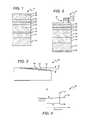
- FIG. 1is sectional view of one embodiment of a laser diode according to the present invention
- FIG. 2is a sectional view of an off-angle substrate according to the present invention.
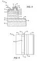
- FIG. 3is a sectional view of another embodiment of a laser diode according to the present invention.
- FIG. 4is a graph showing laser diode threshold current operation
- FIG. 5is a sectional view of still another embodiment of a laser diode according to the present invention.
- FIG. 6is a plan view of another embodiment of a laser diode according to the present invention.
- the present inventionprovides high reliability, high output power nitride-based laser diode characterized by reduced threshold current densities and reduced threshold voltages.
- the present inventionis particularly adapted for laser diodes having a ridge for optical and electrical confinement, with the ridge being etched to level in the laser diode structure that allows for reduced threshold current operation while at the same time allowing for reliable lifetime operation.
- the present inventionis also directed to additional laser diode structural and manufacturing improvements that further enhance laser diode operation.
- first, second, etc.may be used herein to describe various layers, elements, components and/or sections, these layers, elements, components, and/or sections should not be limited by these terms. These terms are only used to distinguish one layer, element, component, or section from another. Thus, a first layer, element, component, or section discussed below could be termed a second element, component, or section without departing from the teachings of the present invention.
- Embodiments of the inventionare described herein with reference to cross-sectional view illustrations that are schematic illustrations of idealized embodiments of the invention. It is understood that many of the layers will have different relative thicknesses compared to those shown and that the laser diodes will have different shapes. Further, variations from the shapes of the illustrations as a result, for example, of manufacturing techniques and/or tolerances are expected. Embodiments of the invention should not be construed as limited to the particular shapes of the regions illustrated herein but are to include deviations in shapes that result, for example, from manufacturing. A region illustrated or described as square or rectangular will typically have rounded or curved features due to normal manufacturing tolerances. Thus, the regions illustrated in the figures are schematic in nature and their shapes are not intended to illustrate the precise shape of a region of a device and are not intended to limit the scope of the invention.
- Embodiments of the present inventionmay be particularly well suited for use in nitride-based devices such as Group III-nitride based laser diodes.
- Group III nitriderefers to those semiconducting compounds formed between nitrogen and the elements in Group III of the periodic table, usually aluminum (Al), gallium (Ga), and/or indium (In).
- Alaluminum
- Gagallium
- Inindium
- the termalso refers to ternary and quaternary compounds, such as AlGaN and AlInGaN.
- the Group III elementscan combine with nitrogen to form binary (e.g., GaN), ternary (e.g., AlGaN and AlInN), and quaternary (e.g., AlInGaN) compounds. These compounds all have empirical formulas in which one mole of nitrogen is combined with a total of one mole of the Group III elements. Accordingly, formulas such as Al x Ga 1 ⁇ x N, where 0 ⁇ 1, are often used to describe them.
- FIG. 1shows one embodiment of a laser diode 10 according to the present invention at an intermediate fabrication stage.
- a single laser diode 10is shown, it is understood that many laser diodes are typically fabricated on a single substrate wafer, with the devices then being separated into individual devices using known processes, such as facet cleaving to form die arrays and die separation using scribe and break processes.
- the layers of laser diodes according to the present inventioncan be formed or grown on a substrate wafer using known fabrication processes such as growth in a reactor by metalorganic chemical vapor deposition (MOCVD).
- MOCVDmetalorganic chemical vapor deposition
- the present inventioncan be utilized with many different laser diode structures arranged in different ways, with the laser diode 10 being only one example of such a laser diode structure.
- the laser diode 10comprises a substrate 12 that can be made of many different materials such as sapphire, silicon carbide, or GaN.
- the preferred laser diode 10is formed on a free-standing GaN substrate lateral epitaxial overgrown (LEO) pendeo GaN, or a substrate with a lateral epitaxial overgrowth layer on the a substrate such as silicon or silicon carbide.
- the substratecan be GaN grown by hybrid vapor-phase epitaxy (HVPE)
- Threading dislocation densities in GaN based epitaxial structurescan enhance the operating characteristics and if the initial epitaxial layers are grown with low threading dislocation densities it will spread to the layers that follow. It is preferable that the threading dislocation densities be less than approximately 5 ⁇ 10 5 cm ⁇ 2 in the laser diode's GaN based epitaxial layers, which can reduce threshold current. This can also reduce dopant (Mg) diffusion to the active region, which can improve reliability.
- Different fabrication processescan be used according to the present invention to achieve low dislocation densities such as pendeo or lateral epitaxy overgrowth of GaN. This can be done as one of the first layers in the laser diode.
- a GaN layeris formed on a substrate, such as sapphire. Pillars with top surface mesas are etched in the GaN layer and partially into the sapphire substrate. GaN is grown over the pillars and substrate, and GaN grows on the mesas of the pillars as well as laterally outward. The GaN grown on the mesas has substantially the same dislocation density as the pillar below, but the threading dislocation from the pillar does not propagate to the laterally grown GaN. The laterally grown GaN grows together between adjacent pillars to form a reduced dislocation density surface. This reduced dislocation will spread to subsequent growth layers.
- FIG. 2illustrates one embodiment of an off-angle cut substrate 40 according to the present invention and it is understood that for ease of understanding, the substrate 40 and its features are not to scale.
- the substrate 40is cut with off-angle 42 , the crystalline nature of the substrate results in the formation of steps 44 along the cut surface with step edges 46 between the steps 44 . If the off-angle 44 of the cut can be controlled, a consistent and repeatable step surface can be formed.
- Atoms from the growth gasattach to the growing surface in a low energy configuration, and for substrate 40 when the growth atoms 48 encounter the surface of the step edge 46 they attach at the step edge 46 as a low energy configuration.
- the film or epitaxial layergrow smoothly in a step flow mode growth by the atoms 48 first attaching to the step edges 46 and then terrace growing across the surface of each step 44 . This in turn provides for a smoother interface for the layers grown on the substrate 40 , including the quantum well growth.
- the off-angle 44 of the substrate 40can be at different angles with a suitable range of angles being between 0.1 to 5°, and a preferred off-angle being 0.5 to 1°.
- An n-type contact layer 14is grown on the substrate 12 and comprises a semiconductor material suitable for spreading current from an n-contact to the active region.
- a semiconductor material suitable for spreading current from an n-contact to the active regioncan be used for the n-type contact layer, with a preferred material being n-type doped GaN, with a suitable dopant being silicon (Si).
- the n-contactcan be formed on the substrate 12 and currents from an electrical signal applied to the n-contact conducts through the substrate 12 and n-contact layer 14 , to the active region of the laser diode 10 .
- a lateral geometrycan be used for contacting the device.
- the laser diode 10can be etched to form a mesa in the n-type contact layer 14 and the n-contact is deposited on the contact layer mesa. Current spreads from the contact, through the n-type contact layer 14 and to the laser diode's active region.
- laser diodes formed on a conductive substratecan effectively spread current without the n-type contact layer 14 , and that these embodiments can be arranged without the n-type contact layer 14 . It is further understood that other embodiments of the present invention can have the substrate removed, and contact can be made directly to the epitaxial layers.
- a compliance layer 16can be included on the n-type layer to help reduce the strain between the n-contact layer 14 and subsequent epitaxial layers of the laser diode 10 .
- the compliance layercan be made of many different materials, with a preferred compliance layer being made of an n-type InGaN with Si doping.
- a waveguiding element 18is included on the compliance layer 16 with a preferred waveguiding element being a strained layer superlattice (SLS) structure comprising layers of semiconductor material. Many different materials can be used for the n-type SLS layers with preferred materials being AlGaN/GaN with Si-doping of the GaN layer(s) only.
- SLSstrained layer superlattice
- n-type guiding layer 20is formed on the n-type SLS 18 with the guiding layer also referred to as a separate confinement heterostructure (SCH).
- the n-type SCH 20serves as part of the light path to the edges of the laser diode 10 and ultimately out the emission edge of the laser diode 10 .
- the light from the active region traveling toward the waveguiding elements (n-type SLS 20 and the p-type SLS described below)is reflected, and light traveling toward the laser diode's edges is reflected until stimulated emission is out one of the edges.
- the n-type SCH layer 20 and p-type SCH layerserve as the primary reflection cavity for this reflected light.
- the n-type SCH 20can comprise many different materials with a preferred material being n-type doped GaN grown with Si doping.
- the active region 22is grown on the n-type SCH layer 20 and the active region can comprise different layers arranged in different ways, with a preferred active region comprising a MQW region that can have different numbers of quantum wells and barrier layers.
- MQW active region 22comprises three quantum wells and associated barrier layers made of InGaN.
- the laser diode 10further comprises an electron blocking layer 24 formed on the MQW active region 22 .
- the blocking layer 24comprises a material that blocks electrons from passing from the MOW active region 22 into the p-type SCH layer (described below), but lets holes pass through to form the p-type SCH layer to the MQW active region 22 . By blocking electrons, the blocking layer encourages recombination in the MQW active region 22 .
- the blocking layercan be made of many different materials, with a suitable material being p-type A 1 GaN with Mg doping.
- a p-type guiding layer or SCH 26is formed on the electron blocking layer 24 .
- the p-type SCHcan be made of many different materials with a suitable material being p-type GaN with Mg doping.
- a second waveguiding element 28is included on the p-type SCH layer 26 , with the waveguiding element 28 preferably comprising a p-type SLS made of AlGaN/GaN layers with Mg doping the GaN layer only.
- a p-type contact layer 30is included on the p-type SLS.
- the contact layercan also comprise many different materials, with a preferred material being p-type GaN with Mg-doping.
- the laser diode 10 as shown in FIG. 1can then have a p-contact and n-contact deposited on it using known techniques such as photolithography and liftoff techniques.
- the p-contactis typically deposited on the p-type contact layer 30 and the n-contact can be on either the substrate (for conductive substrates) or on the n-contact mesa as further described below. More commonly, however, a ridge etched from the laser diodes top surface. The ridge provides electrical and optical confinement and index-guiding for the particular wavelength of light generated by the laser diode's active region. This in turn can allow for operation at lower threshold currents and voltages.
- the ridgecan be formed using known mask and etching processes with a suitable etching process being plasma reactive ion etching (RIE).
- RIEplasma reactive ion etching
- the p- and n-contactscan be made of many different materials such as gold (Au), nickel (Ni), platinum (Pt), Al, or combinations thereof.
- FIG. 3shows the laser diode 10 at a subsequent fabrication step having a ridge 32 etched from its top surface with the ridge arranged to provide optical and electrical confinement, which can result in lower threshold and current operation.
- the ridge 32can have many different widths with some ridges being 2 ⁇ m or less wide, and preferably in the range of 1.7 to 2 ⁇ m.
- the etching of the ridge 32can be to different depths in the laser diode 10 , with a preferred depth according to the present invention being through the p-contact layer 30 and a portion of the p-type SLS 28 .
- the ridge 32is etched through the p-type SLS 28 until the etch reaches 1 to 2 ⁇ m (microns) above the p-type SCH 26 .
- the graph 50shows the threshold current operation for a laser diode over time, with the laser diode having a ridge.
- the first plot 52shows a threshold current operation for a laser diode according to the present invention having a ridge etched to 1-2 ⁇ m from the p-type SCH. As shown, the threshold current remains relatively constant over time.
- the second line 54shows the threshold current operation for a laser diode with the ridge etched into the p-type SCH.
- the threshold current at the beginning of operationis lower than that of line 52 , but the reliability of the laser diode is negatively impacted by this etch depth.
- a failure point 56is reached where the threshold current increases dramatically and laser diode fails to operate.
- FIG. 3shows the laser diode 10 at a subsequent fabrication step having a ridge 32 etched from its top surface with the ridge arranged to provide optical and electrical confinement, which can result in lower threshold and current operation.
- the ridge 32can have many different widths with some ridges being 2 ⁇ m or less wide, and preferably in the range of 1.7 to 2 ⁇ m.
- the etching of the ridge 32can be to different depths in the laser diode 10 , with a preferred depth according to the present invention being through the p-contact layer 30 and a portion of the p-type SLS 28 .
- the ridge 32is etched through the p-type SLS 28 until the etch reaches 0.1 to 0.2 ⁇ m (microns) above the p-type SCH 26 .
- the graph 50shows the threshold current operation for a laser diode over time, with the laser diode having a ridge.
- the first plot 52shows a threshold current operation for a laser diode according to the present invention having a ridge etched to 0.1 to 0.2 ⁇ m from the p-type SCH. As shown, the threshold current remains relatively constant over time.
- the second line 54shows the threshold current operation for a laser diode with the ridge etched into the p-type SCH.
- the threshold current at the beginning of operationis lower than that of line 52 , but the reliability of the laser diode is negatively impacted by this etch depth.
- a failure point 56is reached where the threshold current increases dramatically and laser diode fails to operate.
- the laser diode 10also comprises a p-contact (ohmic metal) 34 on the top surface of the ridge 32 , which is the p-contact layer 30 .
- An n-contact (ohmic metal) 36can also be included on the substrate 12 for those embodiments having a conductive substrate.
- the p- and n-contacts 34 , 36can be made of many different materials, with preferred p-contacts being made of platinum (Pt), gold (Au), nickel (Ni), or combinations thereof, and preferred n-contacts being made of titanium (Ti), Al, Au, Ni, or combinations thereof.
- the p- and n-contactscan also be deposited using know methods.
- FIG. 5shows another embodiment of a laser diode 60 according to the present invention having the same or similar layers as those shown in FIGS. 1 and 3 and described above. For those same and similar layers, the same reference numbers are used with the understanding that the description of those layers above applies to laser diode 60 .
- the laser diode 60has a non-conductive substrate 62 and for electrical contact to be made to the n-contact layer 64 , a contact n-mesa 66 is formed by etching the layers above the n-contact layer 64 .
- n-contact 68is deposited on the mesa, and when a bias is applied across the p- and n-contacts 34 , 68 current from the n-contact 68 spreads into the n-contact layer 64 and to the active region 22 .
- the ridge 32 for laser diode 60can have the same etch depth (0.1 to 0.2 ⁇ m) to provide low voltage and threshold current operation.
- FIG. 6shows a top view of a laser diode 90 (without insulating layer, bond pad or wire bond) according to the present invention, having a ridge 92 , p-mesa 94 , n-mesa 96 , p-contact 98 , and n-contact 100 , all of which are arranged similar to corresponding features in laser diode 10 and 60 described above and shown in FIGS. 3 and 5 .
- the individual laser diodesundergo a cleaving to form the laser diodes on the wafer into rows of diode arrays, with the cleaving forming the edge facets on opposite sides of the laser diode.
- the ridge 92 , p- and n-mesas 94 , 96 , p-contact 98 , and n-contact 100can all be formed prior to cleaving. According to the present invention, however, the p-contact 98 should not run completely along the ridge 92 when formed on the ridge 92 . By instead providing a setback 102 the danger of p-contact 98 peel-off during cleaving and operation is reduced. In one embodiment according to the present invention, the p-contact 98 has a setback 102 that is in the range of approximately 5-10 ⁇ m, although other setback lengths can also be used.
- the p-contactis a combination of Ni and Au, and because light does not pass through the p-contact, it does not need to be transparent.
- annealing of the completed laser structureis completed in a nitrogen gas only to provide good ohmic contact.
- the p-contactdoes not need to be oxidized during annealing to be made transparent, so oxidizing gas (oxygen) is not needed as part of the annealing gas.
- oxidizing gasoxygen
- Different anneal time frames and temperaturescan be used, with the preferred annealing process taking approximately 10 minutes at a temperature range of 600-700° C., with a preferred temperature being approximately 650° C.
- the plasma cleanercan comprise different compounds, with a preferred compound comprising an O 2 plasma cleaning process.
- the plasma cleaning processcan be performed in commercially available systems such as the Technics Model PE-IIA Plasma Etching System or SPI Plasma-Etch II Plasma Etcher, Cleaner and Asher.
- the asher descumshould be used on the facets after cleaving and prior to high reflectivity (HR) and anti-reflectivity (AR) coating of the facets.
- the plasma cleaningshould also be used following photolithography and wet etch steps such as following etching of the ridge or n-type mesa or photolithography for formation of the n-contact or pad metal, all which are described above.
- the plasma cleaningshould also be used when mounting the laser diode in commercially available packaging or can.
- the canshould be cleaned with a plasma cleaner and the laser diode can then be mounted in the can.
- the laser diodecan be bonded with AuSn solder or similar material. After mounting the can should again be subjected to plasma cleaning, then filled with an inert gas (N 2 , argon, etc.) and then hermitically sealed. This cleaning process reduces the contaminants that can remain after mounting of the laser diode and sealing of the can.
Landscapes
- Physics & Mathematics (AREA)
- Optics & Photonics (AREA)
- Chemical & Material Sciences (AREA)
- Engineering & Computer Science (AREA)
- Nanotechnology (AREA)
- Life Sciences & Earth Sciences (AREA)
- Biophysics (AREA)
- Crystallography & Structural Chemistry (AREA)
- Condensed Matter Physics & Semiconductors (AREA)
- General Physics & Mathematics (AREA)
- Electromagnetism (AREA)
- Semiconductor Lasers (AREA)
Abstract
Description
Claims (20)
Priority Applications (2)
| Application Number | Priority Date | Filing Date | Title |
|---|---|---|---|
| US11/600,617US7813400B2 (en) | 2006-11-15 | 2006-11-15 | Group-III nitride based laser diode and method for fabricating same |
| US12/880,392US8050304B2 (en) | 2006-11-15 | 2010-09-13 | Group-III nitride based laser diode and method for fabricating same |
Applications Claiming Priority (1)
| Application Number | Priority Date | Filing Date | Title |
|---|---|---|---|
| US11/600,617US7813400B2 (en) | 2006-11-15 | 2006-11-15 | Group-III nitride based laser diode and method for fabricating same |
Related Child Applications (1)
| Application Number | Title | Priority Date | Filing Date |
|---|---|---|---|
| US12/880,392DivisionUS8050304B2 (en) | 2006-11-15 | 2010-09-13 | Group-III nitride based laser diode and method for fabricating same |
Publications (2)
| Publication Number | Publication Date |
|---|---|
| US20080112453A1 US20080112453A1 (en) | 2008-05-15 |
| US7813400B2true US7813400B2 (en) | 2010-10-12 |
Family
ID=39369175
Family Applications (2)
| Application Number | Title | Priority Date | Filing Date |
|---|---|---|---|
| US11/600,617ActiveUS7813400B2 (en) | 2006-11-15 | 2006-11-15 | Group-III nitride based laser diode and method for fabricating same |
| US12/880,392ActiveUS8050304B2 (en) | 2006-11-15 | 2010-09-13 | Group-III nitride based laser diode and method for fabricating same |
Family Applications After (1)
| Application Number | Title | Priority Date | Filing Date |
|---|---|---|---|
| US12/880,392ActiveUS8050304B2 (en) | 2006-11-15 | 2010-09-13 | Group-III nitride based laser diode and method for fabricating same |
Country Status (1)
| Country | Link |
|---|---|
| US (2) | US7813400B2 (en) |
Cited By (17)
| Publication number | Priority date | Publication date | Assignee | Title |
|---|---|---|---|---|
| US8395165B2 (en) | 2011-07-08 | 2013-03-12 | Bridelux, Inc. | Laterally contacted blue LED with superlattice current spreading layer |
| US8564010B2 (en) | 2011-08-04 | 2013-10-22 | Toshiba Techno Center Inc. | Distributed current blocking structures for light emitting diodes |
| US8664679B2 (en) | 2011-09-29 | 2014-03-04 | Toshiba Techno Center Inc. | Light emitting devices having light coupling layers with recessed electrodes |
| US8686430B2 (en) | 2011-09-07 | 2014-04-01 | Toshiba Techno Center Inc. | Buffer layer for GaN-on-Si LED |
| US8698163B2 (en) | 2011-09-29 | 2014-04-15 | Toshiba Techno Center Inc. | P-type doping layers for use with light emitting devices |
| US8853668B2 (en) | 2011-09-29 | 2014-10-07 | Kabushiki Kaisha Toshiba | Light emitting regions for use with light emitting devices |
| US8865565B2 (en) | 2011-08-02 | 2014-10-21 | Kabushiki Kaisha Toshiba | LED having a low defect N-type layer that has grown on a silicon substrate |
| US8916906B2 (en) | 2011-07-29 | 2014-12-23 | Kabushiki Kaisha Toshiba | Boron-containing buffer layer for growing gallium nitride on silicon |
| US9012921B2 (en) | 2011-09-29 | 2015-04-21 | Kabushiki Kaisha Toshiba | Light emitting devices having light coupling layers |
| US9012939B2 (en) | 2011-08-02 | 2015-04-21 | Kabushiki Kaisha Toshiba | N-type gallium-nitride layer having multiple conductive intervening layers |
| US9130068B2 (en) | 2011-09-29 | 2015-09-08 | Manutius Ip, Inc. | Light emitting devices having dislocation density maintaining buffer layers |
| US9142743B2 (en) | 2011-08-02 | 2015-09-22 | Kabushiki Kaisha Toshiba | High temperature gold-free wafer bonding for light emitting diodes |
| US9159869B2 (en) | 2011-08-03 | 2015-10-13 | Kabushiki Kaisha Toshiba | LED on silicon substrate using zinc-sulfide as buffer layer |
| US9178114B2 (en) | 2011-09-29 | 2015-11-03 | Manutius Ip, Inc. | P-type doping layers for use with light emitting devices |
| US9343641B2 (en) | 2011-08-02 | 2016-05-17 | Manutius Ip, Inc. | Non-reactive barrier metal for eutectic bonding process |
| US9617656B2 (en) | 2011-07-25 | 2017-04-11 | Toshiba Corporation | Nucleation of aluminum nitride on a silicon substrate using an ammonia preflow |
| US10256385B2 (en) | 2007-10-31 | 2019-04-09 | Cree, Inc. | Light emitting die (LED) packages and related methods |
Families Citing this family (4)
| Publication number | Priority date | Publication date | Assignee | Title |
|---|---|---|---|---|
| US8358673B2 (en)* | 2011-02-17 | 2013-01-22 | Corning Incorporated | Strain balanced laser diode |
| CN108598233A (en)* | 2018-04-18 | 2018-09-28 | 湘能华磊光电股份有限公司 | A kind of LED outer layer growths method |
| CN110335927B (en)* | 2019-07-11 | 2020-10-30 | 马鞍山杰生半导体有限公司 | Ultraviolet LED and preparation method thereof |
| CN118174142B (en)* | 2024-05-14 | 2024-08-30 | 武汉鑫威源电子科技有限公司 | Blue laser and preparation method thereof, and preparation method of epitaxial structure |
Citations (35)
| Publication number | Priority date | Publication date | Assignee | Title |
|---|---|---|---|---|
| US4152044A (en) | 1977-06-17 | 1979-05-01 | International Telephone And Telegraph Corporation | Galium aluminum arsenide graded index waveguide |
| FR2586844A1 (en) | 1985-08-27 | 1987-03-06 | Sofrela Sa | Signalling device using light-emitting diodes |
| US4675575A (en) | 1984-07-13 | 1987-06-23 | E & G Enterprises | Light-emitting diode assemblies and systems therefore |
| US5477436A (en) | 1992-08-29 | 1995-12-19 | Robert Bosch Gmbh | Illuminating device for motor vehicles |
| US5592501A (en) | 1994-09-20 | 1997-01-07 | Cree Research, Inc. | Low-strain laser structures with group III nitride active layers |
| FR2759188A1 (en) | 1997-01-31 | 1998-08-07 | Thery Hindrick | Signal light used for controlling road traffic |
| WO1998056043A1 (en) | 1997-06-03 | 1998-12-10 | Daimlerchrysler Ag | Semiconductor component and method for producing the same |
| EP0936682A1 (en) | 1996-07-29 | 1999-08-18 | Nichia Chemical Industries, Ltd. | Light emitting device and display device |
| US6046464A (en) | 1995-03-29 | 2000-04-04 | North Carolina State University | Integrated heterostructures of group III-V nitride semiconductor materials including epitaxial ohmic contact comprising multiple quantum well |
| US6330111B1 (en) | 2000-06-13 | 2001-12-11 | Kenneth J. Myers, Edward Greenberg | Lighting elements including light emitting diodes, microprism sheet, reflector, and diffusing agent |
| US6331915B1 (en) | 2000-06-13 | 2001-12-18 | Kenneth J. Myers | Lighting element including light emitting diodes, microprism sheet, reflector, and diffusing agent |
| WO2002011212A1 (en) | 2000-07-27 | 2002-02-07 | Caldus Semiconductor, Inc. | W/wc/tac ohmic and rectifying contacts on sic |
| US20020015013A1 (en) | 2000-06-28 | 2002-02-07 | Larry Ragle | Integrated color LED chip |
| FR2814220A1 (en) | 2000-09-18 | 2002-03-22 | Koito Mfg Co Ltd | VEHICLE LAMP COMPRISING SEVERAL PHOTOEMISSIVE DIODES |
| US20020054495A1 (en) | 2000-09-18 | 2002-05-09 | Koito Manufacturing Co., Ltd. | Vehicle lamp |
| US20030015708A1 (en) | 2001-07-23 | 2003-01-23 | Primit Parikh | Gallium nitride based diodes with low forward voltage and low reverse current operation |
| US20030020069A1 (en)* | 2001-07-25 | 2003-01-30 | Motorola, Inc. | Structure and method for optimizing transmission media through dielectric layering and doping in semiconductor structures and devices utilizing the formation of a compliant substrate |
| WO2003044870A1 (en) | 2001-11-22 | 2003-05-30 | Mireille Georges | Light-emitting diode illuminating optical device |
| US20030165169A1 (en)* | 2002-03-01 | 2003-09-04 | Opnext Japan, Inc. | Semiconductor laser diode and optical module |
| EP1349202A2 (en) | 2002-03-28 | 2003-10-01 | Rohm Co., Ltd. | Semiconductor device and method of manufacturing the same |
| WO2003080763A1 (en) | 2002-03-25 | 2003-10-02 | Philips Intellectual Property & Standards Gmbh | Tri-color white light led lamp |
| US6746889B1 (en) | 2001-03-27 | 2004-06-08 | Emcore Corporation | Optoelectronic device with improved light extraction |
| US6784463B2 (en) | 1997-06-03 | 2004-08-31 | Lumileds Lighting U.S., Llc | III-Phospide and III-Arsenide flip chip light-emitting devices |
| US20040207313A1 (en) | 2003-04-21 | 2004-10-21 | Sharp Kabushiki Kaisha | LED device and portable telephone, digital camera and LCD apparatus using the same |
| US20050173692A1 (en) | 2002-12-27 | 2005-08-11 | Park Young H. | Vertical GaN light emitting diode and method for manufacturing the same |
| US6932497B1 (en) | 2003-12-17 | 2005-08-23 | Jean-San Huang | Signal light and rear-view mirror arrangement |
| US20060034576A1 (en)* | 2004-08-16 | 2006-02-16 | Merritt Scott A | Superluminescent diodes having high output power and reduced internal reflections |
| US20060081862A1 (en) | 2004-10-14 | 2006-04-20 | Chua Janet B Y | Device and method for emitting output light using quantum dots and non-quantum fluorescent material |
| EP1653255A2 (en) | 2004-10-29 | 2006-05-03 | Pentair Water Pool and Spa, Inc. | Selectable beam lens for underwater light |
| EP1681509A1 (en) | 2005-01-17 | 2006-07-19 | Omron Corporation | Luminescent light source and luminescent source array |
| US7087936B2 (en) | 2003-04-30 | 2006-08-08 | Cree, Inc. | Methods of forming light-emitting devices having an antireflective layer that has a graded index of refraction |
| WO2007005844A2 (en) | 2005-07-05 | 2007-01-11 | International Rectifier Corporation | Schottky diode with improved surge capability |
| US20070025231A1 (en)* | 2005-07-29 | 2007-02-01 | Masanao Ochiai | Semiconductor laser device |
| US20070090383A1 (en) | 2000-12-28 | 2007-04-26 | Toyoda Gosei Co., Ltd. | Light emitting device |
| US20080036364A1 (en) | 2006-08-10 | 2008-02-14 | Intematix Corporation | Two-phase yellow phosphor with self-adjusting emission wavelength |
Family Cites Families (12)
| Publication number | Priority date | Publication date | Assignee | Title |
|---|---|---|---|---|
| US678A (en)* | 1838-04-05 | bennet woodcroft | ||
| US4933302A (en)* | 1989-04-19 | 1990-06-12 | International Business Machines Corporation | Formation of laser mirror facets and integration of optoelectronics |
| US6744800B1 (en)* | 1998-12-30 | 2004-06-01 | Xerox Corporation | Method and structure for nitride based laser diode arrays on an insulating substrate |
| JP4024994B2 (en)* | 2000-06-30 | 2007-12-19 | 株式会社東芝 | Semiconductor light emitting device |
| US6833564B2 (en) | 2001-11-02 | 2004-12-21 | Lumileds Lighting U.S., Llc | Indium gallium nitride separate confinement heterostructure light emitting devices |
| US6969874B1 (en)* | 2003-06-12 | 2005-11-29 | Sandia Corporation | Flip-chip light emitting diode with resonant optical microcavity |
| US20050077535A1 (en) | 2003-10-08 | 2005-04-14 | Joinscan Electronics Co., Ltd | LED and its manufacturing process |
| TWI291770B (en) | 2003-11-14 | 2007-12-21 | Hon Hai Prec Ind Co Ltd | Surface light source device and light emitting diode |
| JP4442216B2 (en) | 2003-12-19 | 2010-03-31 | 豊田合成株式会社 | LED lamp device |
| US7170111B2 (en) | 2004-02-05 | 2007-01-30 | Cree, Inc. | Nitride heterojunction transistors having charge-transfer induced energy barriers and methods of fabricating the same |
| WO2005104247A1 (en) | 2004-04-19 | 2005-11-03 | Matsushita Electric Industrial Co., Ltd. | Method for fabricating led illumination light source and led illumination light source |
| TWI255566B (en) | 2005-03-04 | 2006-05-21 | Jemitek Electronics Corp | Led |
- 2006
- 2006-11-15USUS11/600,617patent/US7813400B2/enactiveActive
- 2010
- 2010-09-13USUS12/880,392patent/US8050304B2/enactiveActive
Patent Citations (38)
| Publication number | Priority date | Publication date | Assignee | Title |
|---|---|---|---|---|
| US4152044A (en) | 1977-06-17 | 1979-05-01 | International Telephone And Telegraph Corporation | Galium aluminum arsenide graded index waveguide |
| US4675575A (en) | 1984-07-13 | 1987-06-23 | E & G Enterprises | Light-emitting diode assemblies and systems therefore |
| FR2586844A1 (en) | 1985-08-27 | 1987-03-06 | Sofrela Sa | Signalling device using light-emitting diodes |
| US5477436A (en) | 1992-08-29 | 1995-12-19 | Robert Bosch Gmbh | Illuminating device for motor vehicles |
| US5592501A (en) | 1994-09-20 | 1997-01-07 | Cree Research, Inc. | Low-strain laser structures with group III nitride active layers |
| US5838706A (en) | 1994-09-20 | 1998-11-17 | Cree Research, Inc. | Low-strain laser structures with group III nitride active layers |
| US6046464A (en) | 1995-03-29 | 2000-04-04 | North Carolina State University | Integrated heterostructures of group III-V nitride semiconductor materials including epitaxial ohmic contact comprising multiple quantum well |
| EP0936682A1 (en) | 1996-07-29 | 1999-08-18 | Nichia Chemical Industries, Ltd. | Light emitting device and display device |
| FR2759188A1 (en) | 1997-01-31 | 1998-08-07 | Thery Hindrick | Signal light used for controlling road traffic |
| WO1998056043A1 (en) | 1997-06-03 | 1998-12-10 | Daimlerchrysler Ag | Semiconductor component and method for producing the same |
| US6784463B2 (en) | 1997-06-03 | 2004-08-31 | Lumileds Lighting U.S., Llc | III-Phospide and III-Arsenide flip chip light-emitting devices |
| US6330111B1 (en) | 2000-06-13 | 2001-12-11 | Kenneth J. Myers, Edward Greenberg | Lighting elements including light emitting diodes, microprism sheet, reflector, and diffusing agent |
| US6331915B1 (en) | 2000-06-13 | 2001-12-18 | Kenneth J. Myers | Lighting element including light emitting diodes, microprism sheet, reflector, and diffusing agent |
| US20020015013A1 (en) | 2000-06-28 | 2002-02-07 | Larry Ragle | Integrated color LED chip |
| WO2002011212A1 (en) | 2000-07-27 | 2002-02-07 | Caldus Semiconductor, Inc. | W/wc/tac ohmic and rectifying contacts on sic |
| FR2814220A1 (en) | 2000-09-18 | 2002-03-22 | Koito Mfg Co Ltd | VEHICLE LAMP COMPRISING SEVERAL PHOTOEMISSIVE DIODES |
| US20020054495A1 (en) | 2000-09-18 | 2002-05-09 | Koito Manufacturing Co., Ltd. | Vehicle lamp |
| US6657393B2 (en) | 2000-09-18 | 2003-12-02 | Koito Manufacturing Co., Ltd. | Vehicle lamp having light sources with LEDs arranged in two groups |
| US20070090383A1 (en) | 2000-12-28 | 2007-04-26 | Toyoda Gosei Co., Ltd. | Light emitting device |
| US6746889B1 (en) | 2001-03-27 | 2004-06-08 | Emcore Corporation | Optoelectronic device with improved light extraction |
| US20030015708A1 (en) | 2001-07-23 | 2003-01-23 | Primit Parikh | Gallium nitride based diodes with low forward voltage and low reverse current operation |
| US20030020069A1 (en)* | 2001-07-25 | 2003-01-30 | Motorola, Inc. | Structure and method for optimizing transmission media through dielectric layering and doping in semiconductor structures and devices utilizing the formation of a compliant substrate |
| WO2003044870A1 (en) | 2001-11-22 | 2003-05-30 | Mireille Georges | Light-emitting diode illuminating optical device |
| US20030165169A1 (en)* | 2002-03-01 | 2003-09-04 | Opnext Japan, Inc. | Semiconductor laser diode and optical module |
| WO2003080763A1 (en) | 2002-03-25 | 2003-10-02 | Philips Intellectual Property & Standards Gmbh | Tri-color white light led lamp |
| EP1349202A2 (en) | 2002-03-28 | 2003-10-01 | Rohm Co., Ltd. | Semiconductor device and method of manufacturing the same |
| US20050173692A1 (en) | 2002-12-27 | 2005-08-11 | Park Young H. | Vertical GaN light emitting diode and method for manufacturing the same |
| US20040207313A1 (en) | 2003-04-21 | 2004-10-21 | Sharp Kabushiki Kaisha | LED device and portable telephone, digital camera and LCD apparatus using the same |
| US7087936B2 (en) | 2003-04-30 | 2006-08-08 | Cree, Inc. | Methods of forming light-emitting devices having an antireflective layer that has a graded index of refraction |
| US6932497B1 (en) | 2003-12-17 | 2005-08-23 | Jean-San Huang | Signal light and rear-view mirror arrangement |
| US20060034576A1 (en)* | 2004-08-16 | 2006-02-16 | Merritt Scott A | Superluminescent diodes having high output power and reduced internal reflections |
| US20060081862A1 (en) | 2004-10-14 | 2006-04-20 | Chua Janet B Y | Device and method for emitting output light using quantum dots and non-quantum fluorescent material |
| EP1653255A2 (en) | 2004-10-29 | 2006-05-03 | Pentair Water Pool and Spa, Inc. | Selectable beam lens for underwater light |
| US20060158899A1 (en) | 2005-01-17 | 2006-07-20 | Omron Corporation | Luminescent light source and luminescent light source array |
| EP1681509A1 (en) | 2005-01-17 | 2006-07-19 | Omron Corporation | Luminescent light source and luminescent source array |
| WO2007005844A2 (en) | 2005-07-05 | 2007-01-11 | International Rectifier Corporation | Schottky diode with improved surge capability |
| US20070025231A1 (en)* | 2005-07-29 | 2007-02-01 | Masanao Ochiai | Semiconductor laser device |
| US20080036364A1 (en) | 2006-08-10 | 2008-02-14 | Intematix Corporation | Two-phase yellow phosphor with self-adjusting emission wavelength |
Non-Patent Citations (55)
| Title |
|---|
| (From related application) Canadian Patent Application No. 2,454,310, Office Action dated Feb. 9, 2010. |
| Asbeck et al."Enhancement of Base Conductivity Via the Piezoelectric Effect in AlGaN/GaN HBTs", Solid State Electronics, Elsevier Science Pub. Barking GB, vol. 44, No. 2, Feb. 1, 2000 pp. 211-219, XP004186190. |
| Copending U.S. Appl. No. 11/443,741, date: Jun. 14, 2007. |
| Copending U.S. Appl. No. 11/685,761, date: Mar. 13, 2007. |
| Copending U.S. Appl. No. 11/939,059, date: Nov. 13, 2007. |
| European Communication from related European Appl. 02 798 906.0-1235, Dated Feb. 6, 2009. |
| European Search Report from related European Application No. 07254498.4, received on Feb. 11, 2010. |
| European Search Report re related EP Appl. 08160129.6.2222, Dated: Dec. 15, 2008. |
| European Search Report re related European Application No. 08253301.9-2222, Feb. 24, 2009. |
| European Search Report, Feb. 24, 2009, re related European Application No. EP 08253301. |
| International Search Report for PCT/US2008/004453, Date: Sep. 9, 2008. |
| Kim J K et al. "Strongly Enhanced Phosphor Efficiency in GaInN White Light-Emitting Diodes Using Remote Phosphor Configuration and Diffuse Reflector Cup", Japanese Journal of Applied Physics, Japan Society of Applied Physics, Tokyo, JP, vol. 44, No. 20-23, Jan. 1, 2005, XP-001236966. |
| Notice of First Office Action from related China Patent Application No. 200710142217.6, dated: Jun. 22, 2009. |
| Notice Requesting Submission of Opinion re related Korean Application No. 10-2004-7001033, dated: Mar. 9, 2009. |
| Offical Notice of Final Decision of Rejection re related Japanesse Patent Appl. No. 2003-529535, Dated: Jan. 6, 2009. |
| Office Action from related U.S. Appl. No. 11/600,618, dated: Feb. 4, 2010. |
| Official Communication from the EPO regarding related European Application 08253301.9, dated: Nov. 17, 2009. |
| PCT Search Report and Written Opinion PCT/US2007/086237, date: May 8, 2008 in related application. |
| PCT Search Report and Written Opinion PCT/US2007/086242, Date: Mar. 4, 2008. |
| PCT Search Report and Written Opinion PCT/US2007/12403, Date: Aug. 6, 2008. |
| Publication No. 2005/077535, Publication Date: Apr. 14, 2005. |
| Publication No. 2005/152127, Publication Date: Jul. 14, 2005. |
| Publication No. 2006/220046, Publication Date: Oct. 5, 2006. |
| Publication No. 2008/074032 Publication Date: Mar. 27, 2008. |
| Sakai et al., "Experimental Investigation of Dependence of Electrical Characteristics on Device Parameters in Trench MOS Barrier Schottky Diodes", 1998, International Symposium on Power Semiconductor Devices & ICs, Kyoto, pp. 293-296. |
| Sakai et al., "Experimental Investigation of Dependence of Electrical Characteristics on Device Parameters in Trench Mos Barrier Shottky Diodes", Proceedings of 1998 International Symposium on Power Semiconductor Devices & ICs, Kyoto, pp. 293-296, Jun. 1998. |
| Second Office Action from related Chinese Application No. 200710142217.6, dated: Nov. 6, 2009. |
| Simon et al. "Polarization-Induced 3-Dimensional Electron Slabs in Graded A1GaN Layers", Materials Research Society Symposium Proceedings 2006 Materials Research Society US, vol. 892, Nov. 28, 2005, pp. 417-722. |
| The Second Office Action from People's Republic of China, re: China Application No. 200480027969.2, date: Jul. 4, 2008. |
| U.S. Appl. No. 11/613,692, filed Dec. 20, 2006. |
| U.S. Appl. No. 11/614,180, filed Dec. 21, 2006. |
| U.S. Appl. No. 11/624,811, filed Jan. 19, 2007. |
| U.S. Appl. No. 11/736,799, filed Apr. 18, 2007. |
| U.S. Appl. No. 11/743,754, filed May 3, 2007. |
| U.S. Appl. No. 11/751,982, filed May 22, 2007. |
| U.S. Appl. No. 11/751,990, filed May 22, 2007. |
| U.S. Appl. No. 11/753,103, filed May 24, 2007. |
| U.S. Appl. No. 11/755,153, filed May 30, 2007. |
| U.S. Appl. No. 11/818,818, filed Jun. 14, 2007. |
| U.S. Appl. No. 11/843,243, filed Aug. 22, 2007. |
| U.S. Appl. No. 11/856,421, filed Sep. 17, 2007. |
| U.S. Appl. No. 11/859,048, filed Sep. 21, 2007. |
| U.S. Appl. No. 11/870,679, filed Oct. 11, 2007. |
| U.S. Appl. No. 11/877,038, filed Oct. 23, 2007. |
| U.S. Appl. No. 11/936,163, filed Nov. 7, 2007. |
| U.S. Appl. No. 11/939,047, filed Nov. 13, 2007. |
| U.S. Appl. No. 11/939,052, filed Nov. 13, 2007. |
| U.S. Appl. No. 11/948,041, filed Nov. 30, 2007. |
| U.S. Appl. No. 11/949,222, filed Dec. 3, 2007. |
| U.S. Appl. No. 12/002,429, filed Dec. 4, 2007. |
| U.S. Appl. No. 12/045,729, filed Mar. 11, 2008. |
| U.S. Appl. No. 12/174,053, filed Jul. 16, 2008. |
| Written Opinion for PCT/US2008/004453, Date: Sep. 9, 2008. |
| Zhang AP et al, "Comparison of Gan P-I-N and Schottky Rectifier Performance" IEEE Transactions on Electron Devices, IEEE Inc. New York, US, vol. 48, No. 3, pp. 407-411, Mar. 2001. |
| Zhang et al. "Comparison of GaN P-I-N and Schottky Rectifier Performance", IEEE Transactions on Electron Devices, vol. 48, No. 3, Mar. 2001, pp. 407-411. |
Cited By (21)
| Publication number | Priority date | Publication date | Assignee | Title |
|---|---|---|---|---|
| US10256385B2 (en) | 2007-10-31 | 2019-04-09 | Cree, Inc. | Light emitting die (LED) packages and related methods |
| US8395165B2 (en) | 2011-07-08 | 2013-03-12 | Bridelux, Inc. | Laterally contacted blue LED with superlattice current spreading layer |
| US9617656B2 (en) | 2011-07-25 | 2017-04-11 | Toshiba Corporation | Nucleation of aluminum nitride on a silicon substrate using an ammonia preflow |
| US10174439B2 (en) | 2011-07-25 | 2019-01-08 | Samsung Electronics Co., Ltd. | Nucleation of aluminum nitride on a silicon substrate using an ammonia preflow |
| US8916906B2 (en) | 2011-07-29 | 2014-12-23 | Kabushiki Kaisha Toshiba | Boron-containing buffer layer for growing gallium nitride on silicon |
| US9012939B2 (en) | 2011-08-02 | 2015-04-21 | Kabushiki Kaisha Toshiba | N-type gallium-nitride layer having multiple conductive intervening layers |
| US8865565B2 (en) | 2011-08-02 | 2014-10-21 | Kabushiki Kaisha Toshiba | LED having a low defect N-type layer that has grown on a silicon substrate |
| US9343641B2 (en) | 2011-08-02 | 2016-05-17 | Manutius Ip, Inc. | Non-reactive barrier metal for eutectic bonding process |
| US9142743B2 (en) | 2011-08-02 | 2015-09-22 | Kabushiki Kaisha Toshiba | High temperature gold-free wafer bonding for light emitting diodes |
| US9159869B2 (en) | 2011-08-03 | 2015-10-13 | Kabushiki Kaisha Toshiba | LED on silicon substrate using zinc-sulfide as buffer layer |
| US8564010B2 (en) | 2011-08-04 | 2013-10-22 | Toshiba Techno Center Inc. | Distributed current blocking structures for light emitting diodes |
| US9070833B2 (en) | 2011-08-04 | 2015-06-30 | Kabushiki Kaisha Toshiba | Distributed current blocking structures for light emitting diodes |
| US8686430B2 (en) | 2011-09-07 | 2014-04-01 | Toshiba Techno Center Inc. | Buffer layer for GaN-on-Si LED |
| US8853668B2 (en) | 2011-09-29 | 2014-10-07 | Kabushiki Kaisha Toshiba | Light emitting regions for use with light emitting devices |
| US9178114B2 (en) | 2011-09-29 | 2015-11-03 | Manutius Ip, Inc. | P-type doping layers for use with light emitting devices |
| US9299881B2 (en) | 2011-09-29 | 2016-03-29 | Kabishiki Kaisha Toshiba | Light emitting devices having light coupling layers |
| US9130068B2 (en) | 2011-09-29 | 2015-09-08 | Manutius Ip, Inc. | Light emitting devices having dislocation density maintaining buffer layers |
| US9490392B2 (en) | 2011-09-29 | 2016-11-08 | Toshiba Corporation | P-type doping layers for use with light emitting devices |
| US9012921B2 (en) | 2011-09-29 | 2015-04-21 | Kabushiki Kaisha Toshiba | Light emitting devices having light coupling layers |
| US8698163B2 (en) | 2011-09-29 | 2014-04-15 | Toshiba Techno Center Inc. | P-type doping layers for use with light emitting devices |
| US8664679B2 (en) | 2011-09-29 | 2014-03-04 | Toshiba Techno Center Inc. | Light emitting devices having light coupling layers with recessed electrodes |
Also Published As
| Publication number | Publication date |
|---|---|
| US20100330720A1 (en) | 2010-12-30 |
| US20080112453A1 (en) | 2008-05-15 |
| US8050304B2 (en) | 2011-11-01 |
Similar Documents
| Publication | Publication Date | Title |
|---|---|---|
| US7813400B2 (en) | Group-III nitride based laser diode and method for fabricating same | |
| US8679876B2 (en) | Laser diode and method for fabricating same | |
| US7642626B2 (en) | Semiconductor devices including mesa structures and multiple passivation layers | |
| US6319742B1 (en) | Method of forming nitride based semiconductor layer | |
| US6984841B2 (en) | Nitride semiconductor light emitting element and production thereof | |
| JP4169821B2 (en) | Light emitting diode | |
| JP3316479B2 (en) | Semiconductor device, semiconductor light emitting device, and method of manufacturing semiconductor device | |
| US7485902B2 (en) | Nitride-based semiconductor light-emitting device | |
| US20080049806A1 (en) | Nitride semiconductor laser and method for fabricating the same | |
| US20080217632A1 (en) | Gan-Based III-V Compound Semiconductor Light-Emitting Element and Method for Manufacturing Thereof | |
| US7755101B2 (en) | Semiconductor light emitting device | |
| WO2001095446A1 (en) | Semiconductor laser device, and method of manufacturing the same | |
| JP2008109092A (en) | Semiconductor light emitting device | |
| JP2003124573A (en) | Method of manufacturing semiconductor light emitting device, method of manufacturing semiconductor device, method of manufacturing device, method of growing nitride-based III-V compound semiconductor layer, method of growing semiconductor layer, and method of growing layer | |
| US20060094244A1 (en) | Nitride semiconductor device and fabrication method thereof | |
| JP3460581B2 (en) | Method for growing nitride semiconductor and nitride semiconductor device | |
| US20030227026A1 (en) | Nitride semiconductor, semiconductor device, and manufacturing methods for the same | |
| US20030039286A1 (en) | Method of fabricating semiconductor laser device and semiconductor laser device | |
| JP4493041B2 (en) | Nitride semiconductor light emitting device | |
| JP4617907B2 (en) | Optically integrated semiconductor light emitting device | |
| WO2001039342A1 (en) | Semiconductor light emitting element | |
| JP2001237499A (en) | Manufacturing method of semiconductor light-emitting element | |
| JP3349506B2 (en) | Method of forming nitride-based semiconductor layer | |
| JP2005327753A (en) | Semiconductor laser device | |
| JP2002084036A (en) | Nitride semiconductor laser device |
Legal Events
| Date | Code | Title | Description |
|---|---|---|---|
| AS | Assignment | Owner name:CREE, INC., CALIFORNIA Free format text:ASSIGNMENT OF ASSIGNORS INTEREST;ASSIGNORS:DENBAARS, STEVEN;NAKAMURA, SHUJI;HANSEN, MONICA;REEL/FRAME:018658/0583 Effective date:20061207 | |
| STCF | Information on status: patent grant | Free format text:PATENTED CASE | |
| FPAY | Fee payment | Year of fee payment:4 | |
| MAFP | Maintenance fee payment | Free format text:PAYMENT OF MAINTENANCE FEE, 8TH YEAR, LARGE ENTITY (ORIGINAL EVENT CODE: M1552) Year of fee payment:8 | |
| AS | Assignment | Owner name:CREELED, INC., NORTH CAROLINA Free format text:ASSIGNMENT OF ASSIGNORS INTEREST;ASSIGNOR:CREE, INC.;REEL/FRAME:057017/0311 Effective date:20210301 | |
| AS | Assignment | Owner name:CITIZENS BANK, N.A., MASSACHUSETTS Free format text:SECURITY INTEREST;ASSIGNORS:SMART MODULAR TECHNOLOGIES, INC.;SMART HIGH RELIABILITY SOLUTIONS, LLC;SMART EMBEDDED COMPUTING, INC.;AND OTHERS;REEL/FRAME:058983/0001 Effective date:20220207 | |
| MAFP | Maintenance fee payment | Free format text:PAYMENT OF MAINTENANCE FEE, 12TH YEAR, LARGE ENTITY (ORIGINAL EVENT CODE: M1553); ENTITY STATUS OF PATENT OWNER: LARGE ENTITY Year of fee payment:12 | |
| AS | Assignment | Owner name:SMART MODULAR TECHNOLOGIES, INC., CALIFORNIA Free format text:RELEASE OF PATENT SECURITY INTEREST RECORDED AT R/F 058983/0001;ASSIGNOR:CITIZENS BANK, N.A.;REEL/FRAME:071725/0207 Effective date:20250624 Owner name:SMART EMBEDDED COMPUTING, INC., ARIZONA Free format text:RELEASE OF PATENT SECURITY INTEREST RECORDED AT R/F 058983/0001;ASSIGNOR:CITIZENS BANK, N.A.;REEL/FRAME:071725/0207 Effective date:20250624 Owner name:SMART HIGH RELIABILITY SOLUTIONS LLC, CALIFORNIA Free format text:RELEASE OF PATENT SECURITY INTEREST RECORDED AT R/F 058983/0001;ASSIGNOR:CITIZENS BANK, N.A.;REEL/FRAME:071725/0207 Effective date:20250624 Owner name:CREELED, INC., CALIFORNIA Free format text:RELEASE OF PATENT SECURITY INTEREST RECORDED AT R/F 058983/0001;ASSIGNOR:CITIZENS BANK, N.A.;REEL/FRAME:071725/0207 Effective date:20250624 | |
| AS | Assignment | Owner name:JPMORGAN CHASE BANK, N.A., ILLINOIS Free format text:PATENT SECURITY AGREEMENT;ASSIGNORS:CREELED, INC.;PENGUIN SOLUTIONS CORPORATION (DE);SMART EMBEDDED COMPUTING, INC.;AND OTHERS;REEL/FRAME:071755/0001 Effective date:20250624 |