US7812686B2 - Adjustable low-loss interface - Google Patents
Adjustable low-loss interfaceDownload PDFInfo
- Publication number
- US7812686B2 US7812686B2US12/039,529US3952908AUS7812686B2US 7812686 B2US7812686 B2US 7812686B2US 3952908 AUS3952908 AUS 3952908AUS 7812686 B2US7812686 B2US 7812686B2
- Authority
- US
- United States
- Prior art keywords
- interface
- cavity
- impedance
- energy transmission
- integrated circuit
- Prior art date
- Legal status (The legal status is an assumption and is not a legal conclusion. Google has not performed a legal analysis and makes no representation as to the accuracy of the status listed.)
- Active, expires
Links
- 230000005540biological transmissionEffects0.000claimsabstractdescription53
- 238000002955isolationMethods0.000claimsabstractdescription43
- 230000007704transitionEffects0.000claimsdescription21
- 239000003989dielectric materialSubstances0.000claimsdescription8
- 229910052751metalInorganic materials0.000claimsdescription6
- 239000002184metalSubstances0.000claimsdescription6
- 230000037361pathwayEffects0.000claimsdescription6
- 239000000758substrateSubstances0.000claims3
- 239000000463materialSubstances0.000description17
- 230000008859changeEffects0.000description7
- 230000032258transportEffects0.000description7
- RYGMFSIKBFXOCR-UHFFFAOYSA-NCopperChemical compound[Cu]RYGMFSIKBFXOCR-UHFFFAOYSA-N0.000description5
- 229910052802copperInorganic materials0.000description5
- 239000010949copperSubstances0.000description5
- 230000007423decreaseEffects0.000description4
- PCHJSUWPFVWCPO-UHFFFAOYSA-NgoldChemical compound[Au]PCHJSUWPFVWCPO-UHFFFAOYSA-N0.000description4
- 229910052737goldInorganic materials0.000description4
- 239000010931goldSubstances0.000description4
- 229910052709silverInorganic materials0.000description4
- 239000004332silverSubstances0.000description4
- 229910052782aluminiumInorganic materials0.000description3
- XAGFODPZIPBFFR-UHFFFAOYSA-NaluminiumChemical compound[Al]XAGFODPZIPBFFR-UHFFFAOYSA-N0.000description3
- 238000003780insertionMethods0.000description3
- 230000037431insertionEffects0.000description3
- 239000004677NylonSubstances0.000description2
- BQCADISMDOOEFD-UHFFFAOYSA-NSilverChemical compound[Ag]BQCADISMDOOEFD-UHFFFAOYSA-N0.000description2
- 229910045601alloyInorganic materials0.000description2
- 239000000956alloySubstances0.000description2
- 238000004519manufacturing processMethods0.000description2
- 238000012986modificationMethods0.000description2
- 230000004048modificationEffects0.000description2
- 229920001778nylonPolymers0.000description2
- 239000010935stainless steelSubstances0.000description2
- 229910001220stainless steelInorganic materials0.000description2
- 230000001131transforming effectEffects0.000description2
- 229910001369BrassInorganic materials0.000description1
- 239000006096absorbing agentSubstances0.000description1
- 229910052790berylliumInorganic materials0.000description1
- ATBAMAFKBVZNFJ-UHFFFAOYSA-Nberyllium atomChemical compound[Be]ATBAMAFKBVZNFJ-UHFFFAOYSA-N0.000description1
- 239000010951brassSubstances0.000description1
- 239000000919ceramicSubstances0.000description1
- 239000004020conductorSubstances0.000description1
- 230000003993interactionEffects0.000description1
- 230000007246mechanismEffects0.000description1
- 150000002739metalsChemical class0.000description1
- 239000012811non-conductive materialSubstances0.000description1
- 230000010355oscillationEffects0.000description1
- 239000004033plasticSubstances0.000description1
- 229920003023plasticPolymers0.000description1
- 239000000523sampleSubstances0.000description1
- 230000035945sensitivityEffects0.000description1
- 230000003746surface roughnessEffects0.000description1
- 230000009466transformationEffects0.000description1
- WFKWXMTUELFFGS-UHFFFAOYSA-NtungstenChemical compound[W]WFKWXMTUELFFGS-UHFFFAOYSA-N0.000description1
- 229910052721tungstenInorganic materials0.000description1
- 239000010937tungstenSubstances0.000description1
Images

Classifications
- H—ELECTRICITY
- H01—ELECTRIC ELEMENTS
- H01P—WAVEGUIDES; RESONATORS, LINES, OR OTHER DEVICES OF THE WAVEGUIDE TYPE
- H01P5/00—Coupling devices of the waveguide type
- H01P5/08—Coupling devices of the waveguide type for linking dissimilar lines or devices
- H01P5/10—Coupling devices of the waveguide type for linking dissimilar lines or devices for coupling balanced lines or devices with unbalanced lines or devices
- H01P5/107—Hollow-waveguide/strip-line transitions
Definitions
- the present inventiongenerally relates to an interface for use, for example, between an integrated circuit and a waveguide. More particularly, the present invention relates to an impedance matching interface such as a step launch that transports or transforms energy from an integrated circuit, such as a monolithic microwave integrated circuit. In one exemplary embodiment, the impedance matching capability is adjustable.
- circuits and other electronic devicesthat produce energy waves, such as electromagnetic waves and microwaves. These circuits produce energy waves that are delivered to a destination through different wires, guides, and other mediums.
- Transitioning microwave signals from one mode to another or interfacing to another mediumis “lossy.” By being lossy, a portion of the signal is lost as it travels through the circuits, wires, and other mediums. Stated another way, a signal entering a lossy material will be greater at the point of entry than at the point of exit.
- Waveguidesare structures that define a cavity that carries energy waves to a particular destination. Unfortunately, signal loss is still problematic with certain waves because the connection or interface between the circuit generating the energy waves and the waveguide can be lossy itself.
- the interfaces between a waveguide and an integrated circuittend to be lossy in part, due to the initial transition from a circuit such as a MMIC to the interface.
- This initial transition between an integrated circuit and an interfaceis lossy due to the impedance difference between the integrated circuit and interface.
- One way to reduce this initial lossis to closely match the impedance of the MMIC or other integrated circuit with the interface at the transition point.
- MMICshave some of the greatest and most noticeable amounts of signal loss due to due to the types of interfaces used to connect MMICs to other energy transmission devices, such as waveguides. Moreover, impedance miss-matches from the MMIC to the waveguide enhance signal losses. For example, the impedance of the MMIC, for example fifty ohms, may not match the impedance of the connected waveguide, which is much higher, typically several hundred ohms higher than the impendence of the MMIC. Further, the MMIC and waveguide also likely have different modes of energy wave propagation.
- Interconnects between a MMIC and waveguidecomprise numerous structures that include wirebond, microstrips, pins, and other devices to connect a circuit to a waveguide or another structure. Each part of a matching network has associated loss. These interfaces also attempt to match and transform the impedance of the MMIC to the impedance at the waveguide. These types of interfaces are known generally as “impedance matching interfaces” or “impedance matching and transforming interfaces” and these interfaces transform impedance and wave mode propagation of the energy traveling through the interface.
- Rippleis unwanted gain variation versus frequence due to the mismatch of impedances at two electronic devices, such as a microstrip track and MMIC or from a microstrip to a suspended stripline or from a suspended stripline to a waveguide.
- a mismatchthere is a return wave that generates a standing wave. This standing wave is what causes the ripple versus frequency.
- an interfacefor connecting two devices where energy is transmitted or received there between.
- the interface of the present inventionis a low-loss interface that directly connects a MMIC to a waveguide without the use of dielectric materials.
- the interfacefurther comprises an isolation wall located between an input region and output region of one of the devices that transmits or receives energy.
- a turning screw or other adjustable memberis provided to increase or decrease the cavity volume within the interface and/or the waveguide cavity to most closely match the impedance at the connection point between the circuit and interface.
- FIG. 1illustrates a cross sectional view of an interface connecting a MMIC to a waveguide wherein the interface is a single ridge interface comprising an isolation wall and an adjustable turning screw in accordance with an exemplary embodiment of the present invention
- FIG. 2illustrates a cross sectional view of an interface with a double ridge step launch in accordance with another exemplary embodiment of the present invention
- FIG. 3illustrates a cross sectional view of an interface connecting a MMIC to a waveguide wherein the interface has a ninety degree transference of energy in accordance with another exemplary embodiment of the present invention
- FIG. 4illustrates a cross sectional view of an interface in accordance with another exemplary embodiment of the present invention
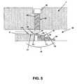
- FIG. 5illustrates a cross sectional view of an interface with a turning screw being on the opposing side of a step launch according to another exemplary embodiment of the present invention
- FIG. 6illustrates a cross sectional view of an interface connected to two electronic circuits and an interface according to another exemplary embodiment of the present invention.
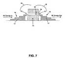
- FIG. 7illustrates a side view of two interfaces located on the input and output side of a circuit according to another exemplary embodiment of the present invention.
- an interface for connecting an integrated circuit to an energy transmission device such as a waveguideis disclosed.
- the interfacewill be referred to as interface 10 .
- an interface 10is provided between an integrated circuit 11 and an energy transmission device 13 .
- Certain exemplary interfaces 10 that may be used with the present inventionare disclosed in co-pending and commonly owned U.S. patent application Ser. No. 11/853,287 entitled “Low-Loss Interface” which is incorporated in its entirety by reference.
- Interface 10connects integrated circuit 11 , such as a MMIC, to another energy transmission device 13 such as a waveguide. While the terms integrated circuit 11 and energy transmission device 13 are used herein, it should be understood that interface 10 can connect any energy transmission, reception, or similar device and fall within the scope of the present invention. With particular reference to FIGS. 1 and 2 , interface 10 , integrated circuit 11 , and energy transmission device 13 are typically located within another structure 7 that surrounds various components that comprise the system that interface 10 , integrated circuit 11 , and energy transmission device 13 are part of. Structure 7 can comprise a lid and base as discussed below or structure 7 can be a single unit with space for integrated circuit 11 , interface 10 and energy transmission device 13 . In certain exemplary embodiments, structure 7 is constructed from a metal such as aluminum or copper. In other exemplary embodiments, structure 7 is plated with another metal such as gold or silver.
- integrated circuit 11is a monolithic microwave integrated circuit (MMIC).
- MMICmonolithic microwave integrated circuit
- Integrated circuit 11is part of an electronic system and is connected to another electronic device such as a microstrip 5 (or any other electronic device) at an input region 14 and further connected to energy transmission device 13 at an output region 16 .
- Input region 14 and output region 16can be any know device that is capable of forming an electronic connection such as a wirebond. Further, various known connection mechanisms such as ribbon bonds can be used to connect input region 14 and output region 16 to other devices as explained herein.
- integrated circuit 11comprises discrete components on a circuit board such as power amplifiers, low noise amplifiers, detectors, limiters, isolators, switches, filters, multiplexers, couplers, and the like.
- Integrated circuit 11can be any type of circuit, circuit board, printed circuit board, integrated circuit, discrete component, combination of discrete components, or other type of device or medium that produces, receives, or transfers electronic waves such as microwave signals.
- circuitor “integrated circuit” are not limited to devices with discrete components on a circuit board, but rather includes any device that passes energy waves such as wires, cables, or waveguides.
- energy transmission device 13can be any type of device or medium configured to transport energy.
- energy transmission device 13is a waveguide that transports microwave energy waves.
- energy transmission device 13comprises wires, cables or other devices configured to transport and guide energy waves from one source to another.
- Yet other exemplary energy transmission device 13comprises other integrated circuits such as a MMIC or anything else that transport electrical energy.
- interface 10comprises a stepped transition defining an interface cavity 18 that increases in size up to the size of a waveguide cavity 20 .
- the stepped transitionmay comprise a step launch 15 defining a body 17 which in turn defines a series of ridges or steps 30 , 32 , 34 , and 36 disposed between interface cavity 18 and waveguide cavity 20 .
- Body 17further defines a space 19 that leads into waveguide cavity 20 .
- step launch 15is configured such that space 19 between successive steps 30 , 32 , 34 , etc. increases in the direction from interface cavity 18 to waveguide cavity 20 .
- the depth and/or height of each stepmay be the same from step to step so that each step may resemble the step before it.
- the height of each stepis 0.5 mm at Ka band frequencies. At lower frequencies, the height can more significant, an exemplary height is 3 mm. In other embodiments, however, the depth and/or height of each step may vary compared to one or more other steps in the step launch. Steps are not limited to being monotonic. Moreover, the corner or edges of steps 30 , 32 , 34 , and 36 are rounded to the range of 0.001 mm to 1 mm in one exemplary embodiment which further reduces loss.
- Step launch 15can be constructed from any conductive material that minimizes loss.
- step launch 15is gold plated.
- step launch 15is comprised of silver, copper, aluminum, plated plastics, plated ceramics, various metals and/or alloys, and/or other similar materials with low resistance. Any materials configured to facilitate impedance matching and reduce signal loss can be used to construct step launch 15 .
- step launch 15comprises a single ridge step launch (e.g., steps 30 , 32 , 34 , etc. on one side only). Step launch 15 is configured to provide a stepped transition from the impedance of integrated circuit 11 to the impedance of energy transmission device 13 .
- interface 10comprises double ridge device (e.g. steps 30 , 32 , 34 etc. on two sides) and may be formed from two pieces of energy transmission material such as a lid 26 and a package base 28 connected together.
- lid 26 and base 28are formed in such a shape that when these two parts are properly aligned they form space 19 that comprises step launch 15 of interface 10 and that further comprises energy transmission device 13 .
- the two housing portionsare shaped such that when they are brought together they form a recess that is interface 10 and energy transmission device 13 and where interface 10 is a gradual transition to waveguide cavity 20 .
- Interface 10can be located on lid 26 or on the base 28 as shown. When interface 10 is disposed on lid 26 , insertion loss may be less than 0.2 dB when energy frequency is increased from 15 GHz to 38.6 GHz. In various other exemplary embodiments, interface 10 forms an abrupt mechanical transition from integrated circuit 11 to the waveguide cavity or other energy transmission device 13 .
- step launch 15comprises a double ridge step launch to accommodate waveguide cavities or other similar energy transmission devices with various sizes and impedance requirements.
- the number and size of stepsis typically related to the frequency. The lower the frequency the larger the size of waveguide cavity 20 in that the larger waveguide 20 , the greater number of steps may be used to match the output impedance of integrated circuit 11 to waveguide cavity 20 . Having more steps will reduce minimize return loss and RF discontinues in the transition.
- the steps length and heightcan be selected to reduce loss depending on the application that interface 10 is used for.
- the second ridge or step of the step launchcan be built to be longer than the first ridge as shown.
- the insertion losshas been shown to be less than 0.2 dB from 27 GHz to 38.6 GHz. In other embodiments, adjusting the various dimensions of the ridges or steps has reduced insertion loss to less than 0.1 dB based on an energy frequency increase from 27 GHz to 38.4 GHz.
- step launch 15can comprise a smooth, slopped transition without steps.
- the angle of the transitioncan be whatever angle needed to accommodate energy transmission device 13 .
- Certain exemplary stepped transitions for various step launches 15include, but are not limited to, triangular, exponential, or Klopfenstein tapers.
- Interface 10may comprise an isolation wall 22 that is located between input region 14 and output region 16 .
- Isolation wall 22is any structure that separates input region 14 from output region 15 and is configured to reduce ripple and other interference between input region 14 and output region 16 to reduce loss.
- Certain exemplary isolation walls 22comprise metal structures, microwave absorbers, and dielectrics. Reducing the ripple at this location also reduces the overall loss of energy waves at the transition between integrated circuit 11 and energy transmission device 13 .
- isolation wall 22isolates the input and output pads (i.e. the input region 14 and output region 16 ) present on integrated circuit 11 such as a MMIC. Isolating the input region 14 and output region 16 of a MMIC reduces unwanted feedback. This makes for more stable MMIC or other integrated circuit 11 that will not oscillate.
- isolation wall 22prevents loss at high frequencies and increases performance.
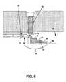
- Isolation wall 22can be constructed from the same material as structure 7 such as aluminum or copper or it can be constructed of another material and plated with silver or gold. In this exemplary embodiment, isolation wall 22 is approximately ten millimeters thick. In other exemplary embodiments, isolation wall 22 is approximately ten to fifty millimeters thick. Any size or shape of isolation wall 22 that is configured to reduce ripple by isolating input region 14 from output region 16 falls within the scope of the present invention. Further, isolation wall 22 can be a simply a vertical member depicted in FIGS. 3 , 4 , and 5 or it can have a flange 24 or other similar horizontal member as depicted in FIGS. 1 and 2 .
- isolation wall 22is placed at a distance of approximately 0.5 to 0.05 millimeters above integrated circuit 11 . In other exemplary embodiments, isolation wall is placed at a distance in the range of 0.25 millimeters above integrated circuit 11 or anywhere in a range of approximately 0.25 to 0.5 millimeters above integrated circuit 11 . In yet other exemplary embodiments, other height ranges can be used and fall within the scope of the present invention. Further, in an exemplary embodiment when a MMIC is used as integrated circuit 11 , the isolation wall was placed immediately after the last gain stage on the MMIC and before the output wirebond. However, isolation wall 22 can be placed at any location along interface 10 and fall within the scope of the present invention.
- interface 10further comprises a wirebond 12 directly connecting step launch 15 to integrated circuit 11 .
- wirebond 12can be any shape and consist of any number of wirebond.
- Wirebond 12may comprise an electrically conductive low-loss material and wirebond 12 can comprise leads, pins, ribbons or anything else that connects two or more devices that transmit energy.
- Certain exemplary materialsinclude, but are not limited to, gold, silver, copper, various alloys, beryllium, copper, tungsten, and/or other similar materials with high conductivity and low resistance.
- wirebond 12any device or piece of material configured to transport energy can be used as wirebond 12 .
- Certain exemplary wirebondare 0.15 millimeters to 25 millimeters in length.
- Wirebond 12can be any size suitable for the particular location that interface 10 is used for. For example, if a long distance is required between integrated circuit 11 and step launch 15 , wirebond 12 can be longer to accommodate that distance.
- wirebond 12can be a probe, a coaxial pin, cable or another type of device with a coaxial configuration.
- wirebond 12is a spongy material such as disclosed in the co-pending patent application noted above entitled “Low-Loss Interface” wherein such application was previously incorporated in its entirety by reference.
- wirebond 12can be connected to interface 10 at various locations. For example, as depicted in the exemplary embodiment of FIGS. 1 and 2 , wirebond 12 is connected directly from the integrated circuit 11 output region 16 to isolation wall 22 . However, in the exemplary embodiment depicted in FIGS. 3 , 4 , and 5 , wirebond 12 is directly connected to integrated circuit 11 and to step launch 15 .
- isolation wall 22can be used in conjunction with interface 10 and fall within the scope of the present invention.
- two, three or more isolation walls 22can be used and placed in various positions at various heights above integrated circuit 11 or other components.
- Numerous isolation wallscan also be constructed of different materials, have different sizes, or they can be constructed of the same material and have the same size.
- interface 10further comprises turning screw 38 .
- Turning screw 38is any adjustable member configured to adjust the size or volume of interface cavity 18 to minimize loss by closely matching the impedance of integrated circuit 11 with interface 10 at the connection between interface 10 and integrated circuit 11 . The impedance is matched by adjusting the volume of interface cavity 18 to provide an interface cavity 18 with the correct dimensions to reduce the most loss.
- turning screw 38is constructed from stainless steel, brass, or nylon. The screw can be constructed from electrically conductive or non-conductive material.
- the tip of turning screw 38 that is disposed within interface cavitycan be constructed from the same or similar material as the remainder of turning screw 38 .
- the shaft of turning screw 38could be constructed from nylon while the tip is constructed of stainless steel.
- any other device that adjusts interface cavity 18 (or waveguide cavity 20 )falls within the scope of the present invention.
- Other exemplary devicesinclude adjustable pins, bolts, or other similar cylindrical structures.
- a rack and pinion devicecould also be used instead of turning screw 38 in another exemplary embodiment of the invention.
- multiple turning screws or other similar devices as described hereincan be used. In this exemplary embodiment, screws are placed directly over two or more of steps 30 , 32 , 34 , and 36 to adjust the spaces in interface cavity 18 and space 19 above steps 30 , 32 , 34 , and 36 .
- turning screw 38can be omitted and the size of interface cavity 18 can be adjusted by moving structure 7 or by moving lid 26 or package base 28 .
- turning screw 38 and other similar devicescan be omitted entirely and interface cavity 18 can have a constant non-adjustable size.
- turning screw 38comprises a shaft 40 connected to a head 42 .
- Turning screw 38is adjustable and adjusts the size of interface cavity 18 to create a size that enables interface 10 to have the least amount of loss depending on the particular application that interface 10 is used for.
- turning screw 38enables the user to tune the impedance matching between interface 10 and integrated circuit 11 at the connection point.
- turning screw 38may be adjusted until the interface cavity 18 is such that the least amount of loss occurs. Loss is reduced because interface cavity 18 near output region 16 is adjusted to allow the impedance of integrated circuit 11 to most closely match the impedance of cavity 13 at the location of interface cavity 18 .
- the impedance of interface 10 at step launch 15may be sixty ohms while the impedance of integrated circuit 11 is fifty ohms. However, if the size of interface cavity 18 is adjusted to eight millimeters, the impedance of interface 10 at step launch 15 may be matched exactly to be fifty ohms. Adjusting turning screw 38 allows for this precise impedance matching to occur.
- turning screw 38enables interface 10 to be customized to reduce loss depending on the specific location in which it is used.
- turning screw 38can be removed and the space occupied by turning screw 38 can be filled with another material.
- turning screw 38can be connected to interface 10 or oriented in numerous different ways to adjust interface cavity 18 . As shown in FIGS. 1 , 2 , and 5 , turning screw 38 is seated within body 7 or lid 26 respectively in order to place shaft 40 directly above output region 16 on the opposing side of interface 10 . In other exemplary embodiments depicted in FIGS. 3 and 4 , turning screw 38 is oriented in such a manner as to tune from the bottom of the waveguide cavity. Turning screw 38 can be located anywhere on interface 10 and fall within the scope of the present invention.
- interface 10serves as a pathway for various energy waves, such as RF waves and microwaves.
- Interface 10provides impedance and mode transformation to meet the desired impedances and modes of integrated circuit 11 and energy transmission device 13 .
- the impedance of step launch 15changes with first step 30 and second step 32 (and possibly additional steps 34 , 36 ) to eventually match the impedance and mode of energy wave propagation of energy transmission device 13 on the opposing end of interface 10 .
- first step 30 and second step 32and possibly additional steps 34 , 36
- this disclosurealso contemplates changing the size of the opening in the horizontal direction.
- the size of the cavity in step launch 15may change from end to end by increasing the height, width, diameter, and/or making any other suitable change to the size or volume of the cavity.
- a MMICproduces microwave energy that experiences a certain first impedance of fifty ohms.
- the impedance of interface 10has been adjusted to be fifty ohms be changing the size of interface cavity 18 using turning screw 38 .
- the energy produced by the MMICis produced at output region 16 with less ripple than normal MMIC's due to the placement of isolation wall 22 between input region 14 and output region 16 .
- This energy experiencing a fifty ohm impedanceis passed into interface 10 through wirebond 12 and then enters step launch 15 .
- the energy and associated energy waves produced by the MMICis able to easily transition from the MMIC to interface 10 due to turning screw 38 being set to allow interface cavity 18 to have the size or volume to reduce loss the most.
- step launch 15is configured to handle energy experiencing, for example a fifty ohm impedance with minimal loss.
- the impedance of step launch 15gradually changes until it is equal to the impedance of the energy transmission device 13 . Therefore, the impedance the energy experiences as it travels through step launch 15 gradually changes until the impedance the energy experiences is equal to that it will experience in energy transmission device 13 .
- graduallymeans changing less abruptly than a direct change from the MMIC impedance to the waveguide impedance in one place.
- the energy transmission device 13may have a second impedance of three-hundred and seventy ohms and interface 10 must match the fifty ohm impedance of integrated circuit 11 to the much larger impedance of energy transmission device 13 with minimal loss.
- the impedanceis changed gradually on interface 10 depending on the number of transition steps or ridges defined by step launch 15 until it reaches three-hundred and seventy seven ohms, the impedance of the energy transmission device 15 .
- the impedancemay slightly change with each step, 30 , 32 , and 34 as it travels through step launch 15 .
- the impedancemight start out at fifty ohms at step 30 , change to one hundred and fifty ohms at step 32 , and finally to three-hundred and seventy seven ohms at step 34 .
- the impedanceis changed by the slope of step launch 15 . Gradually changing the impedance the energy experiences minimizes loss as the energy travels through interface 10 .
- a mode of wave propagation for energy transmission device 13such as a waveguide may be TE 10 (Transverse Electric, 10) while integrated circuit 11 such as a MMIC may have a microstrip mode of wave propagation of quasi-TEM (Traverse Electromagnetic).
- Interface 10is configured to change the mode of wave propagation from integrated circuit 11 to energy transmission device 13 in the same manner it changes the impedance.
- interface 10can be used in connection with an electrical system that comprises more than one circuit such as integrated circuit 11 .
- interface 10can be part of an electrical system that comprises two circuits such as integrated circuit 11 and a secondary circuit 44 .
- the circuitsare arranged serially, however, in other embodiments, other arrangements of circuits are contemplated.
- Certain exemplary secondary circuitscomprise a microwave circuit or network.
- isolation wall 22is placed over integrated circuit 11 .
- isolation wall 22could be placed anywhere as noted above and more than one isolation wall 22 can be used and fall within the scope of the present invention.
- secondary circuit 44may can be any circuit or other electronic device such as a MMIC or it may comprise discrete components on a circuit board such as power amplifiers, low noise amplifiers, low noise amplifiers, detectors, limiters, isolators, switches, filters, multiplexers, couplers, and the like.
- Secondary circuitcan be any type of circuit, circuit board, printed circuit board, integrated circuit, discrete component, combination of discrete components, or other type of device or medium that produces, receives, or transfers electronic waves such as microwave signals.
- circuitor “integrated circuit” are not limited to devices with discrete components on a circuit board, but rather include any device that passes energy waves such as wires, cables, or waveguides.
- interface 10can be used with an electrical system.
- interface 10can be on both the input and output sides (relative to the direction of energy flow, such as RF energy) of integrated circuit 11 or a plurality of circuits such as a secondary circuit 44 discussed above.
- Both interface 10 's located on input region 14 and output region 16 of integrated circuit 11comprise step launches 15 with a number of steps, however any step launch 15 or other similar device can be used and fall within the scope of the present invention.
- isolation wall 22is placed at either the input or output side of integrated circuit 11 or two isolation walls 22 can be used on both sides. Alternatively, a single isolation wall 22 can be used and placed above the middle of integrated circuit 11 . As shown in this exemplary embodiment, a direct wirebond 12 interface is used to connect both the input and output regions of integrated circuit 11 to step launches 15 .
- interface 10is capable of matching the impedance of energy transmission device 13 with little or no signal loss.
- Interface 10does not require the use of dielectric materials and/or microstrips in one exemplary embodiment. In other exemplary embodiments, some dielectric materials may be used in the manufacture of various components of interface 10 .
Landscapes
- Microwave Amplifiers (AREA)
- Semiconductor Integrated Circuits (AREA)
Abstract
Description
Claims (24)
Priority Applications (4)
| Application Number | Priority Date | Filing Date | Title |
|---|---|---|---|
| US12/039,529US7812686B2 (en) | 2008-02-28 | 2008-02-28 | Adjustable low-loss interface |
| PCT/US2008/075969WO2009036134A1 (en) | 2007-09-11 | 2008-09-11 | Low-loss interface |
| EP08799446.3AEP2201679B1 (en) | 2007-09-11 | 2008-09-11 | Low-loss interface |
| TW098106087ATWI533502B (en) | 2008-02-28 | 2009-02-26 | Adjustable low-loss interface |
Applications Claiming Priority (1)
| Application Number | Priority Date | Filing Date | Title |
|---|---|---|---|
| US12/039,529US7812686B2 (en) | 2008-02-28 | 2008-02-28 | Adjustable low-loss interface |
Publications (2)
| Publication Number | Publication Date |
|---|---|
| US20090219107A1 US20090219107A1 (en) | 2009-09-03 |
| US7812686B2true US7812686B2 (en) | 2010-10-12 |
Family
ID=41012739
Family Applications (1)
| Application Number | Title | Priority Date | Filing Date |
|---|---|---|---|
| US12/039,529Active2028-05-15US7812686B2 (en) | 2007-09-11 | 2008-02-28 | Adjustable low-loss interface |
Country Status (2)
| Country | Link |
|---|---|
| US (1) | US7812686B2 (en) |
| TW (1) | TWI533502B (en) |
Cited By (153)
| Publication number | Priority date | Publication date | Assignee | Title |
|---|---|---|---|---|
| US20130271235A1 (en)* | 2011-01-25 | 2013-10-17 | Nec Corporation | Coaxial waveguide converter and ridge waveguide |
| US9544006B2 (en) | 2014-11-20 | 2017-01-10 | At&T Intellectual Property I, L.P. | Transmission device with mode division multiplexing and methods for use therewith |
| US9577306B2 (en) | 2014-10-21 | 2017-02-21 | At&T Intellectual Property I, L.P. | Guided-wave transmission device and methods for use therewith |
| US9596001B2 (en) | 2014-10-21 | 2017-03-14 | At&T Intellectual Property I, L.P. | Apparatus for providing communication services and methods thereof |
| US9608692B2 (en) | 2015-06-11 | 2017-03-28 | At&T Intellectual Property I, L.P. | Repeater and methods for use therewith |
| US9608740B2 (en) | 2015-07-15 | 2017-03-28 | At&T Intellectual Property I, L.P. | Method and apparatus for launching a wave mode that mitigates interference |
| US9615269B2 (en) | 2014-10-02 | 2017-04-04 | At&T Intellectual Property I, L.P. | Method and apparatus that provides fault tolerance in a communication network |
| US9627768B2 (en) | 2014-10-21 | 2017-04-18 | At&T Intellectual Property I, L.P. | Guided-wave transmission device with non-fundamental mode propagation and methods for use therewith |
| US9628116B2 (en) | 2015-07-14 | 2017-04-18 | At&T Intellectual Property I, L.P. | Apparatus and methods for transmitting wireless signals |
| US9640850B2 (en) | 2015-06-25 | 2017-05-02 | At&T Intellectual Property I, L.P. | Methods and apparatus for inducing a non-fundamental wave mode on a transmission medium |
| US9654173B2 (en) | 2014-11-20 | 2017-05-16 | At&T Intellectual Property I, L.P. | Apparatus for powering a communication device and methods thereof |
| US9653770B2 (en) | 2014-10-21 | 2017-05-16 | At&T Intellectual Property I, L.P. | Guided wave coupler, coupling module and methods for use therewith |
| US9661505B2 (en) | 2013-11-06 | 2017-05-23 | At&T Intellectual Property I, L.P. | Surface-wave communications and methods thereof |
| US9667317B2 (en) | 2015-06-15 | 2017-05-30 | At&T Intellectual Property I, L.P. | Method and apparatus for providing security using network traffic adjustments |
| US9685992B2 (en) | 2014-10-03 | 2017-06-20 | At&T Intellectual Property I, L.P. | Circuit panel network and methods thereof |
| US9692101B2 (en) | 2014-08-26 | 2017-06-27 | At&T Intellectual Property I, L.P. | Guided wave couplers for coupling electromagnetic waves between a waveguide surface and a surface of a wire |
| US9699785B2 (en) | 2012-12-05 | 2017-07-04 | At&T Intellectual Property I, L.P. | Backhaul link for distributed antenna system |
| US9705610B2 (en) | 2014-10-21 | 2017-07-11 | At&T Intellectual Property I, L.P. | Transmission device with impairment compensation and methods for use therewith |
| US9705561B2 (en) | 2015-04-24 | 2017-07-11 | At&T Intellectual Property I, L.P. | Directional coupling device and methods for use therewith |
| US9712350B2 (en) | 2014-11-20 | 2017-07-18 | At&T Intellectual Property I, L.P. | Transmission device with channel equalization and control and methods for use therewith |
| US9722318B2 (en) | 2015-07-14 | 2017-08-01 | At&T Intellectual Property I, L.P. | Method and apparatus for coupling an antenna to a device |
| US9729197B2 (en) | 2015-10-01 | 2017-08-08 | At&T Intellectual Property I, L.P. | Method and apparatus for communicating network management traffic over a network |
| US9735833B2 (en) | 2015-07-31 | 2017-08-15 | At&T Intellectual Property I, L.P. | Method and apparatus for communications management in a neighborhood network |
| US9742462B2 (en) | 2014-12-04 | 2017-08-22 | At&T Intellectual Property I, L.P. | Transmission medium and communication interfaces and methods for use therewith |
| US9749053B2 (en) | 2015-07-23 | 2017-08-29 | At&T Intellectual Property I, L.P. | Node device, repeater and methods for use therewith |
| US9749013B2 (en) | 2015-03-17 | 2017-08-29 | At&T Intellectual Property I, L.P. | Method and apparatus for reducing attenuation of electromagnetic waves guided by a transmission medium |
| US9748626B2 (en) | 2015-05-14 | 2017-08-29 | At&T Intellectual Property I, L.P. | Plurality of cables having different cross-sectional shapes which are bundled together to form a transmission medium |
| US9762289B2 (en) | 2014-10-14 | 2017-09-12 | At&T Intellectual Property I, L.P. | Method and apparatus for transmitting or receiving signals in a transportation system |
| US9768833B2 (en) | 2014-09-15 | 2017-09-19 | At&T Intellectual Property I, L.P. | Method and apparatus for sensing a condition in a transmission medium of electromagnetic waves |
| US9769128B2 (en) | 2015-09-28 | 2017-09-19 | At&T Intellectual Property I, L.P. | Method and apparatus for encryption of communications over a network |
| US9769020B2 (en) | 2014-10-21 | 2017-09-19 | At&T Intellectual Property I, L.P. | Method and apparatus for responding to events affecting communications in a communication network |
| US9780834B2 (en) | 2014-10-21 | 2017-10-03 | At&T Intellectual Property I, L.P. | Method and apparatus for transmitting electromagnetic waves |
| US9787412B2 (en) | 2015-06-25 | 2017-10-10 | At&T Intellectual Property I, L.P. | Methods and apparatus for inducing a fundamental wave mode on a transmission medium |
| US9793954B2 (en) | 2015-04-28 | 2017-10-17 | At&T Intellectual Property I, L.P. | Magnetic coupling device and methods for use therewith |
| US9793951B2 (en) | 2015-07-15 | 2017-10-17 | At&T Intellectual Property I, L.P. | Method and apparatus for launching a wave mode that mitigates interference |
| US9793955B2 (en) | 2015-04-24 | 2017-10-17 | At&T Intellectual Property I, Lp | Passive electrical coupling device and methods for use therewith |
| US9794003B2 (en) | 2013-12-10 | 2017-10-17 | At&T Intellectual Property I, L.P. | Quasi-optical coupler |
| US9800327B2 (en) | 2014-11-20 | 2017-10-24 | At&T Intellectual Property I, L.P. | Apparatus for controlling operations of a communication device and methods thereof |
| US9820146B2 (en) | 2015-06-12 | 2017-11-14 | At&T Intellectual Property I, L.P. | Method and apparatus for authentication and identity management of communicating devices |
| US9838078B2 (en) | 2015-07-31 | 2017-12-05 | At&T Intellectual Property I, L.P. | Method and apparatus for exchanging communication signals |
| US9838896B1 (en) | 2016-12-09 | 2017-12-05 | At&T Intellectual Property I, L.P. | Method and apparatus for assessing network coverage |
| US9836957B2 (en) | 2015-07-14 | 2017-12-05 | At&T Intellectual Property I, L.P. | Method and apparatus for communicating with premises equipment |
| US9847850B2 (en) | 2014-10-14 | 2017-12-19 | At&T Intellectual Property I, L.P. | Method and apparatus for adjusting a mode of communication in a communication network |
| US9847566B2 (en) | 2015-07-14 | 2017-12-19 | At&T Intellectual Property I, L.P. | Method and apparatus for adjusting a field of a signal to mitigate interference |
| US9853342B2 (en) | 2015-07-14 | 2017-12-26 | At&T Intellectual Property I, L.P. | Dielectric transmission medium connector and methods for use therewith |
| US9860075B1 (en) | 2016-08-26 | 2018-01-02 | At&T Intellectual Property I, L.P. | Method and communication node for broadband distribution |
| US9865911B2 (en) | 2015-06-25 | 2018-01-09 | At&T Intellectual Property I, L.P. | Waveguide system for slot radiating first electromagnetic waves that are combined into a non-fundamental wave mode second electromagnetic wave on a transmission medium |
| US9866276B2 (en) | 2014-10-10 | 2018-01-09 | At&T Intellectual Property I, L.P. | Method and apparatus for arranging communication sessions in a communication system |
| US9866309B2 (en) | 2015-06-03 | 2018-01-09 | At&T Intellectual Property I, Lp | Host node device and methods for use therewith |
| US9871283B2 (en) | 2015-07-23 | 2018-01-16 | At&T Intellectual Property I, Lp | Transmission medium having a dielectric core comprised of plural members connected by a ball and socket configuration |
| US9871282B2 (en) | 2015-05-14 | 2018-01-16 | At&T Intellectual Property I, L.P. | At least one transmission medium having a dielectric surface that is covered at least in part by a second dielectric |
| US9876570B2 (en) | 2015-02-20 | 2018-01-23 | At&T Intellectual Property I, Lp | Guided-wave transmission device with non-fundamental mode propagation and methods for use therewith |
| US9876264B2 (en) | 2015-10-02 | 2018-01-23 | At&T Intellectual Property I, Lp | Communication system, guided wave switch and methods for use therewith |
| US9876605B1 (en) | 2016-10-21 | 2018-01-23 | At&T Intellectual Property I, L.P. | Launcher and coupling system to support desired guided wave mode |
| US9882277B2 (en) | 2015-10-02 | 2018-01-30 | At&T Intellectual Property I, Lp | Communication device and antenna assembly with actuated gimbal mount |
| US9882257B2 (en) | 2015-07-14 | 2018-01-30 | At&T Intellectual Property I, L.P. | Method and apparatus for launching a wave mode that mitigates interference |
| US9887447B2 (en) | 2015-05-14 | 2018-02-06 | At&T Intellectual Property I, L.P. | Transmission medium having multiple cores and methods for use therewith |
| US9893795B1 (en) | 2016-12-07 | 2018-02-13 | At&T Intellectual Property I, Lp | Method and repeater for broadband distribution |
| US9906269B2 (en) | 2014-09-17 | 2018-02-27 | At&T Intellectual Property I, L.P. | Monitoring and mitigating conditions in a communication network |
| US9904535B2 (en) | 2015-09-14 | 2018-02-27 | At&T Intellectual Property I, L.P. | Method and apparatus for distributing software |
| US9911020B1 (en) | 2016-12-08 | 2018-03-06 | At&T Intellectual Property I, L.P. | Method and apparatus for tracking via a radio frequency identification device |
| US9912382B2 (en) | 2015-06-03 | 2018-03-06 | At&T Intellectual Property I, Lp | Network termination and methods for use therewith |
| US9912419B1 (en) | 2016-08-24 | 2018-03-06 | At&T Intellectual Property I, L.P. | Method and apparatus for managing a fault in a distributed antenna system |
| US9913139B2 (en) | 2015-06-09 | 2018-03-06 | At&T Intellectual Property I, L.P. | Signal fingerprinting for authentication of communicating devices |
| US9912027B2 (en) | 2015-07-23 | 2018-03-06 | At&T Intellectual Property I, L.P. | Method and apparatus for exchanging communication signals |
| US9917341B2 (en) | 2015-05-27 | 2018-03-13 | At&T Intellectual Property I, L.P. | Apparatus and method for launching electromagnetic waves and for modifying radial dimensions of the propagating electromagnetic waves |
| US9930668B2 (en) | 2013-05-31 | 2018-03-27 | At&T Intellectual Property I, L.P. | Remote distributed antenna system |
| US9927517B1 (en) | 2016-12-06 | 2018-03-27 | At&T Intellectual Property I, L.P. | Apparatus and methods for sensing rainfall |
| US9948354B2 (en) | 2015-04-28 | 2018-04-17 | At&T Intellectual Property I, L.P. | Magnetic coupling device with reflective plate and methods for use therewith |
| US9948333B2 (en) | 2015-07-23 | 2018-04-17 | At&T Intellectual Property I, L.P. | Method and apparatus for wireless communications to mitigate interference |
| US9954287B2 (en) | 2014-11-20 | 2018-04-24 | At&T Intellectual Property I, L.P. | Apparatus for converting wireless signals and electromagnetic waves and methods thereof |
| US9967173B2 (en) | 2015-07-31 | 2018-05-08 | At&T Intellectual Property I, L.P. | Method and apparatus for authentication and identity management of communicating devices |
| US9973940B1 (en) | 2017-02-27 | 2018-05-15 | At&T Intellectual Property I, L.P. | Apparatus and methods for dynamic impedance matching of a guided wave launcher |
| US9991580B2 (en) | 2016-10-21 | 2018-06-05 | At&T Intellectual Property I, L.P. | Launcher and coupling system for guided wave mode cancellation |
| US9998870B1 (en) | 2016-12-08 | 2018-06-12 | At&T Intellectual Property I, L.P. | Method and apparatus for proximity sensing |
| US9997819B2 (en) | 2015-06-09 | 2018-06-12 | At&T Intellectual Property I, L.P. | Transmission medium and method for facilitating propagation of electromagnetic waves via a core |
| US9999038B2 (en) | 2013-05-31 | 2018-06-12 | At&T Intellectual Property I, L.P. | Remote distributed antenna system |
| US10009063B2 (en) | 2015-09-16 | 2018-06-26 | At&T Intellectual Property I, L.P. | Method and apparatus for use with a radio distributed antenna system having an out-of-band reference signal |
| US10009067B2 (en) | 2014-12-04 | 2018-06-26 | At&T Intellectual Property I, L.P. | Method and apparatus for configuring a communication interface |
| US10009901B2 (en) | 2015-09-16 | 2018-06-26 | At&T Intellectual Property I, L.P. | Method, apparatus, and computer-readable storage medium for managing utilization of wireless resources between base stations |
| US10009065B2 (en) | 2012-12-05 | 2018-06-26 | At&T Intellectual Property I, L.P. | Backhaul link for distributed antenna system |
| US10020587B2 (en) | 2015-07-31 | 2018-07-10 | At&T Intellectual Property I, L.P. | Radial antenna and methods for use therewith |
| US10020844B2 (en) | 2016-12-06 | 2018-07-10 | T&T Intellectual Property I, L.P. | Method and apparatus for broadcast communication via guided waves |
| US10027397B2 (en) | 2016-12-07 | 2018-07-17 | At&T Intellectual Property I, L.P. | Distributed antenna system and methods for use therewith |
| US10033107B2 (en) | 2015-07-14 | 2018-07-24 | At&T Intellectual Property I, L.P. | Method and apparatus for coupling an antenna to a device |
| US10033108B2 (en) | 2015-07-14 | 2018-07-24 | At&T Intellectual Property I, L.P. | Apparatus and methods for generating an electromagnetic wave having a wave mode that mitigates interference |
| US10044409B2 (en) | 2015-07-14 | 2018-08-07 | At&T Intellectual Property I, L.P. | Transmission medium and methods for use therewith |
| US10069535B2 (en) | 2016-12-08 | 2018-09-04 | At&T Intellectual Property I, L.P. | Apparatus and methods for launching electromagnetic waves having a certain electric field structure |
| US10079661B2 (en) | 2015-09-16 | 2018-09-18 | At&T Intellectual Property I, L.P. | Method and apparatus for use with a radio distributed antenna system having a clock reference |
| US10090606B2 (en) | 2015-07-15 | 2018-10-02 | At&T Intellectual Property I, L.P. | Antenna system with dielectric array and methods for use therewith |
| US10090594B2 (en) | 2016-11-23 | 2018-10-02 | At&T Intellectual Property I, L.P. | Antenna system having structural configurations for assembly |
| US10103422B2 (en) | 2016-12-08 | 2018-10-16 | At&T Intellectual Property I, L.P. | Method and apparatus for mounting network devices |
| US10103801B2 (en) | 2015-06-03 | 2018-10-16 | At&T Intellectual Property I, L.P. | Host node device and methods for use therewith |
| US10136434B2 (en) | 2015-09-16 | 2018-11-20 | At&T Intellectual Property I, L.P. | Method and apparatus for use with a radio distributed antenna system having an ultra-wideband control channel |
| US10135145B2 (en) | 2016-12-06 | 2018-11-20 | At&T Intellectual Property I, L.P. | Apparatus and methods for generating an electromagnetic wave along a transmission medium |
| US10135146B2 (en) | 2016-10-18 | 2018-11-20 | At&T Intellectual Property I, L.P. | Apparatus and methods for launching guided waves via circuits |
| US10135147B2 (en) | 2016-10-18 | 2018-11-20 | At&T Intellectual Property I, L.P. | Apparatus and methods for launching guided waves via an antenna |
| US10139820B2 (en) | 2016-12-07 | 2018-11-27 | At&T Intellectual Property I, L.P. | Method and apparatus for deploying equipment of a communication system |
| US10142086B2 (en) | 2015-06-11 | 2018-11-27 | At&T Intellectual Property I, L.P. | Repeater and methods for use therewith |
| US10144036B2 (en) | 2015-01-30 | 2018-12-04 | At&T Intellectual Property I, L.P. | Method and apparatus for mitigating interference affecting a propagation of electromagnetic waves guided by a transmission medium |
| US10148016B2 (en) | 2015-07-14 | 2018-12-04 | At&T Intellectual Property I, L.P. | Apparatus and methods for communicating utilizing an antenna array |
| US10170840B2 (en) | 2015-07-14 | 2019-01-01 | At&T Intellectual Property I, L.P. | Apparatus and methods for sending or receiving electromagnetic signals |
| US10168695B2 (en) | 2016-12-07 | 2019-01-01 | At&T Intellectual Property I, L.P. | Method and apparatus for controlling an unmanned aircraft |
| US10178445B2 (en) | 2016-11-23 | 2019-01-08 | At&T Intellectual Property I, L.P. | Methods, devices, and systems for load balancing between a plurality of waveguides |
| US10205655B2 (en) | 2015-07-14 | 2019-02-12 | At&T Intellectual Property I, L.P. | Apparatus and methods for communicating utilizing an antenna array and multiple communication paths |
| US10225025B2 (en) | 2016-11-03 | 2019-03-05 | At&T Intellectual Property I, L.P. | Method and apparatus for detecting a fault in a communication system |
| US10224634B2 (en) | 2016-11-03 | 2019-03-05 | At&T Intellectual Property I, L.P. | Methods and apparatus for adjusting an operational characteristic of an antenna |
| US10243270B2 (en) | 2016-12-07 | 2019-03-26 | At&T Intellectual Property I, L.P. | Beam adaptive multi-feed dielectric antenna system and methods for use therewith |
| US10243784B2 (en) | 2014-11-20 | 2019-03-26 | At&T Intellectual Property I, L.P. | System for generating topology information and methods thereof |
| US10264586B2 (en) | 2016-12-09 | 2019-04-16 | At&T Mobility Ii Llc | Cloud-based packet controller and methods for use therewith |
| US10291334B2 (en) | 2016-11-03 | 2019-05-14 | At&T Intellectual Property I, L.P. | System for detecting a fault in a communication system |
| US10291311B2 (en) | 2016-09-09 | 2019-05-14 | At&T Intellectual Property I, L.P. | Method and apparatus for mitigating a fault in a distributed antenna system |
| US10298293B2 (en) | 2017-03-13 | 2019-05-21 | At&T Intellectual Property I, L.P. | Apparatus of communication utilizing wireless network devices |
| US10305190B2 (en) | 2016-12-01 | 2019-05-28 | At&T Intellectual Property I, L.P. | Reflecting dielectric antenna system and methods for use therewith |
| US10312567B2 (en) | 2016-10-26 | 2019-06-04 | At&T Intellectual Property I, L.P. | Launcher with planar strip antenna and methods for use therewith |
| US10320586B2 (en) | 2015-07-14 | 2019-06-11 | At&T Intellectual Property I, L.P. | Apparatus and methods for generating non-interfering electromagnetic waves on an insulated transmission medium |
| US10326494B2 (en) | 2016-12-06 | 2019-06-18 | At&T Intellectual Property I, L.P. | Apparatus for measurement de-embedding and methods for use therewith |
| US10326689B2 (en) | 2016-12-08 | 2019-06-18 | At&T Intellectual Property I, L.P. | Method and system for providing alternative communication paths |
| US10340983B2 (en) | 2016-12-09 | 2019-07-02 | At&T Intellectual Property I, L.P. | Method and apparatus for surveying remote sites via guided wave communications |
| US10340601B2 (en) | 2016-11-23 | 2019-07-02 | At&T Intellectual Property I, L.P. | Multi-antenna system and methods for use therewith |
| US10340603B2 (en) | 2016-11-23 | 2019-07-02 | At&T Intellectual Property I, L.P. | Antenna system having shielded structural configurations for assembly |
| US10340573B2 (en) | 2016-10-26 | 2019-07-02 | At&T Intellectual Property I, L.P. | Launcher with cylindrical coupling device and methods for use therewith |
| US10340600B2 (en) | 2016-10-18 | 2019-07-02 | At&T Intellectual Property I, L.P. | Apparatus and methods for launching guided waves via plural waveguide systems |
| US10341142B2 (en) | 2015-07-14 | 2019-07-02 | At&T Intellectual Property I, L.P. | Apparatus and methods for generating non-interfering electromagnetic waves on an uninsulated conductor |
| US10355367B2 (en) | 2015-10-16 | 2019-07-16 | At&T Intellectual Property I, L.P. | Antenna structure for exchanging wireless signals |
| US10359749B2 (en) | 2016-12-07 | 2019-07-23 | At&T Intellectual Property I, L.P. | Method and apparatus for utilities management via guided wave communication |
| US10361489B2 (en) | 2016-12-01 | 2019-07-23 | At&T Intellectual Property I, L.P. | Dielectric dish antenna system and methods for use therewith |
| US10374316B2 (en) | 2016-10-21 | 2019-08-06 | At&T Intellectual Property I, L.P. | System and dielectric antenna with non-uniform dielectric |
| US10382976B2 (en) | 2016-12-06 | 2019-08-13 | At&T Intellectual Property I, L.P. | Method and apparatus for managing wireless communications based on communication paths and network device positions |
| US10389029B2 (en) | 2016-12-07 | 2019-08-20 | At&T Intellectual Property I, L.P. | Multi-feed dielectric antenna system with core selection and methods for use therewith |
| US10389037B2 (en) | 2016-12-08 | 2019-08-20 | At&T Intellectual Property I, L.P. | Apparatus and methods for selecting sections of an antenna array and use therewith |
| US10411356B2 (en) | 2016-12-08 | 2019-09-10 | At&T Intellectual Property I, L.P. | Apparatus and methods for selectively targeting communication devices with an antenna array |
| US10439675B2 (en) | 2016-12-06 | 2019-10-08 | At&T Intellectual Property I, L.P. | Method and apparatus for repeating guided wave communication signals |
| US10446936B2 (en) | 2016-12-07 | 2019-10-15 | At&T Intellectual Property I, L.P. | Multi-feed dielectric antenna system and methods for use therewith |
| US10498044B2 (en) | 2016-11-03 | 2019-12-03 | At&T Intellectual Property I, L.P. | Apparatus for configuring a surface of an antenna |
| US10530505B2 (en) | 2016-12-08 | 2020-01-07 | At&T Intellectual Property I, L.P. | Apparatus and methods for launching electromagnetic waves along a transmission medium |
| US10535928B2 (en) | 2016-11-23 | 2020-01-14 | At&T Intellectual Property I, L.P. | Antenna system and methods for use therewith |
| US10547348B2 (en) | 2016-12-07 | 2020-01-28 | At&T Intellectual Property I, L.P. | Method and apparatus for switching transmission mediums in a communication system |
| US10601494B2 (en) | 2016-12-08 | 2020-03-24 | At&T Intellectual Property I, L.P. | Dual-band communication device and method for use therewith |
| US10637149B2 (en) | 2016-12-06 | 2020-04-28 | At&T Intellectual Property I, L.P. | Injection molded dielectric antenna and methods for use therewith |
| US10650940B2 (en) | 2015-05-15 | 2020-05-12 | At&T Intellectual Property I, L.P. | Transmission medium having a conductive material and methods for use therewith |
| US10665942B2 (en) | 2015-10-16 | 2020-05-26 | At&T Intellectual Property I, L.P. | Method and apparatus for adjusting wireless communications |
| US10694379B2 (en) | 2016-12-06 | 2020-06-23 | At&T Intellectual Property I, L.P. | Waveguide system with device-based authentication and methods for use therewith |
| US10727599B2 (en) | 2016-12-06 | 2020-07-28 | At&T Intellectual Property I, L.P. | Launcher with slot antenna and methods for use therewith |
| US10755542B2 (en) | 2016-12-06 | 2020-08-25 | At&T Intellectual Property I, L.P. | Method and apparatus for surveillance via guided wave communication |
| US10777873B2 (en) | 2016-12-08 | 2020-09-15 | At&T Intellectual Property I, L.P. | Method and apparatus for mounting network devices |
| US10784670B2 (en) | 2015-07-23 | 2020-09-22 | At&T Intellectual Property I, L.P. | Antenna support for aligning an antenna |
| US10797781B2 (en) | 2015-06-03 | 2020-10-06 | At&T Intellectual Property I, L.P. | Client node device and methods for use therewith |
| US10811767B2 (en) | 2016-10-21 | 2020-10-20 | At&T Intellectual Property I, L.P. | System and dielectric antenna with convex dielectric radome |
| US10819035B2 (en) | 2016-12-06 | 2020-10-27 | At&T Intellectual Property I, L.P. | Launcher with helical antenna and methods for use therewith |
| US10916969B2 (en) | 2016-12-08 | 2021-02-09 | At&T Intellectual Property I, L.P. | Method and apparatus for providing power using an inductive coupling |
| US10938108B2 (en) | 2016-12-08 | 2021-03-02 | At&T Intellectual Property I, L.P. | Frequency selective multi-feed dielectric antenna system and methods for use therewith |
| US11032819B2 (en) | 2016-09-15 | 2021-06-08 | At&T Intellectual Property I, L.P. | Method and apparatus for use with a radio distributed antenna system having a control channel reference signal |
Families Citing this family (5)
| Publication number | Priority date | Publication date | Assignee | Title |
|---|---|---|---|---|
| US9564671B2 (en)* | 2014-12-28 | 2017-02-07 | International Business Machines Corporation | Direct chip to waveguide transition including ring shaped antennas disposed in a thinned periphery of the chip |
| DK3257106T3 (en)* | 2015-02-11 | 2020-11-30 | Fincantieri Spa | WAVE RADIATOR ELEMENT AND METHOD OF MANUFACTURE THEREOF |
| JP6839122B2 (en)* | 2018-03-19 | 2021-03-03 | 日本電信電話株式会社 | High frequency connection structure |
| DE102021117730B4 (en) | 2021-07-08 | 2025-05-15 | Tesat-Spacecom Gmbh & Co. Kg | High-frequency module with impedance matching filter |
| CN113904081B (en)* | 2021-08-26 | 2022-06-28 | 中国电子科技集团公司第二十九研究所 | Grounding terahertz waveguide suspension microstrip conversion circuit connecting device |
Citations (32)
| Publication number | Priority date | Publication date | Assignee | Title |
|---|---|---|---|---|
| US3109054A (en) | 1959-02-09 | 1963-10-29 | Bendix Corp | Stem assembly for electrical components |
| US3987451A (en) | 1975-02-07 | 1976-10-19 | Texas Instruments Incorporated | Beam type planar array antenna system |
| US4608713A (en) | 1983-01-20 | 1986-08-26 | Matsushita Electric Industrial Co., Ltd. | Frequency converter |
| US4678868A (en) | 1979-06-25 | 1987-07-07 | Medtronic, Inc. | Hermetic electrical feedthrough assembly |
| US4868639A (en) | 1986-08-11 | 1989-09-19 | Fujitsu Limited | Semiconductor device having waveguide-coaxial line transformation structure |
| US4947111A (en) | 1989-04-06 | 1990-08-07 | Harris Corporation | Test fixture for multi-GHZ microwave integrated circuits |
| US4967168A (en) | 1989-08-31 | 1990-10-30 | At&T Bell Laboratories | Coaxial-wave guide coupling assemblages |
| US5019829A (en) | 1989-02-08 | 1991-05-28 | Heckman Douglas E | Plug-in package for microwave integrated circuit having cover-mounted antenna |
| US5045820A (en) | 1989-09-27 | 1991-09-03 | Motorola, Inc. | Three-dimensional microwave circuit carrier and integral waveguide coupler |
| US5170142A (en) | 1991-09-09 | 1992-12-08 | Watkins-Johnson Company | Radio frequency feedthrough seal and method |
| US5198786A (en) | 1991-12-04 | 1993-03-30 | Raytheon Company | Waveguide transition circuit |
| US5218373A (en) | 1990-10-01 | 1993-06-08 | Harris Corporation | Hermetically sealed waffle-wall configured assembly including sidewall and cover radiating elements and a base-sealed waveguide window |
| US5223672A (en) | 1990-06-11 | 1993-06-29 | Trw Inc. | Hermetically sealed aluminum package for hybrid microcircuits |
| WO1994000966A1 (en) | 1992-06-22 | 1994-01-06 | Cirqon Technologies Corporation | Ceramic substrates with highly conductive metal vias |
| US5361049A (en)* | 1986-04-14 | 1994-11-01 | The United States Of America As Represented By The Secretary Of The Navy | Transition from double-ridge waveguide to suspended substrate |
| JPH06338709A (en) | 1993-05-31 | 1994-12-06 | Toshiba Corp | Coaxial beads |
| US5376901A (en) | 1993-05-28 | 1994-12-27 | Trw Inc. | Hermetically sealed millimeter waveguide launch transition feedthrough |
| US5468380A (en) | 1989-04-26 | 1995-11-21 | Nippon Kayaku Kabushiki Kaisha | Method for quantitatively measuring sugar-alcohol, column and kit therefor |
| US5488380A (en) | 1991-05-24 | 1996-01-30 | The Boeing Company | Packaging architecture for phased arrays |
| US5678210A (en) | 1995-03-17 | 1997-10-14 | Hughes Electronics | Method and apparatus of coupling a transmitter to a waveguide in a remote ground terminal |
| US5945894A (en) | 1995-03-22 | 1999-08-31 | Murata Manufacturing Co., Ltd. | Dielectric resonator and filter utilizing a non-radiative dielectric waveguide device |
| US5969580A (en)* | 1996-10-01 | 1999-10-19 | Alcatel | Transition between a ridge waveguide and a planar circuit which faces in the same direction |
| EP0954045A2 (en) | 1998-04-28 | 1999-11-03 | TRW Inc. | Millimeter wave ceramic-metal feedthroughs |
| US6232849B1 (en) | 1992-07-23 | 2001-05-15 | Stephen John Flynn | RF waveguide signal transition apparatus |
| US6265950B1 (en) | 1996-09-11 | 2001-07-24 | Robert Bosch Gmbh | Transition from a waveguide to a strip transmission line |
| US6363605B1 (en) | 1999-11-03 | 2002-04-02 | Yi-Chi Shih | Method for fabricating a plurality of non-symmetrical waveguide probes |
| WO2003084001A1 (en) | 2002-04-01 | 2003-10-09 | Gigalane Co., Ltd. | Coaxial connector and connection structure including the same |
| US6911877B2 (en) | 2003-02-26 | 2005-06-28 | Agilent Technologies, Inc. | Coplanar waveguide launch package |
| US7068121B2 (en)* | 2003-06-30 | 2006-06-27 | Tyco Technology Resources | Apparatus for signal transitioning from a device to a waveguide |
| EP1744395A1 (en) | 2005-07-12 | 2007-01-17 | Siemens S.p.A. | Microwave power combiners/splitters on high-loss dielectric substrates |
| US20070096805A1 (en) | 2003-01-03 | 2007-05-03 | Junghyun Kim | Multiple power mode amplifier with bias modulation option and without bypass switches |
| US7486157B2 (en)* | 2005-09-14 | 2009-02-03 | Kabushiki Kaisha Toshiba | Package for high frequency waves containing high frequency electronic circuit |
Family Cites Families (2)
| Publication number | Priority date | Publication date | Assignee | Title |
|---|---|---|---|---|
| US20040038587A1 (en)* | 2002-08-23 | 2004-02-26 | Yeung Hubert K. | High frequency coaxial connector for microcircuit packaging |
| US7011529B2 (en)* | 2004-03-01 | 2006-03-14 | Anritsu Company | Hermetic glass bead assembly having high frequency compensation |
- 2008
- 2008-02-28USUS12/039,529patent/US7812686B2/enactiveActive
- 2009
- 2009-02-26TWTW098106087Apatent/TWI533502B/enactive
Patent Citations (32)
| Publication number | Priority date | Publication date | Assignee | Title |
|---|---|---|---|---|
| US3109054A (en) | 1959-02-09 | 1963-10-29 | Bendix Corp | Stem assembly for electrical components |
| US3987451A (en) | 1975-02-07 | 1976-10-19 | Texas Instruments Incorporated | Beam type planar array antenna system |
| US4678868A (en) | 1979-06-25 | 1987-07-07 | Medtronic, Inc. | Hermetic electrical feedthrough assembly |
| US4608713A (en) | 1983-01-20 | 1986-08-26 | Matsushita Electric Industrial Co., Ltd. | Frequency converter |
| US5361049A (en)* | 1986-04-14 | 1994-11-01 | The United States Of America As Represented By The Secretary Of The Navy | Transition from double-ridge waveguide to suspended substrate |
| US4868639A (en) | 1986-08-11 | 1989-09-19 | Fujitsu Limited | Semiconductor device having waveguide-coaxial line transformation structure |
| US5019829A (en) | 1989-02-08 | 1991-05-28 | Heckman Douglas E | Plug-in package for microwave integrated circuit having cover-mounted antenna |
| US4947111A (en) | 1989-04-06 | 1990-08-07 | Harris Corporation | Test fixture for multi-GHZ microwave integrated circuits |
| US5468380A (en) | 1989-04-26 | 1995-11-21 | Nippon Kayaku Kabushiki Kaisha | Method for quantitatively measuring sugar-alcohol, column and kit therefor |
| US4967168A (en) | 1989-08-31 | 1990-10-30 | At&T Bell Laboratories | Coaxial-wave guide coupling assemblages |
| US5045820A (en) | 1989-09-27 | 1991-09-03 | Motorola, Inc. | Three-dimensional microwave circuit carrier and integral waveguide coupler |
| US5223672A (en) | 1990-06-11 | 1993-06-29 | Trw Inc. | Hermetically sealed aluminum package for hybrid microcircuits |
| US5218373A (en) | 1990-10-01 | 1993-06-08 | Harris Corporation | Hermetically sealed waffle-wall configured assembly including sidewall and cover radiating elements and a base-sealed waveguide window |
| US5488380A (en) | 1991-05-24 | 1996-01-30 | The Boeing Company | Packaging architecture for phased arrays |
| US5170142A (en) | 1991-09-09 | 1992-12-08 | Watkins-Johnson Company | Radio frequency feedthrough seal and method |
| US5198786A (en) | 1991-12-04 | 1993-03-30 | Raytheon Company | Waveguide transition circuit |
| WO1994000966A1 (en) | 1992-06-22 | 1994-01-06 | Cirqon Technologies Corporation | Ceramic substrates with highly conductive metal vias |
| US6232849B1 (en) | 1992-07-23 | 2001-05-15 | Stephen John Flynn | RF waveguide signal transition apparatus |
| US5376901A (en) | 1993-05-28 | 1994-12-27 | Trw Inc. | Hermetically sealed millimeter waveguide launch transition feedthrough |
| JPH06338709A (en) | 1993-05-31 | 1994-12-06 | Toshiba Corp | Coaxial beads |
| US5678210A (en) | 1995-03-17 | 1997-10-14 | Hughes Electronics | Method and apparatus of coupling a transmitter to a waveguide in a remote ground terminal |
| US5945894A (en) | 1995-03-22 | 1999-08-31 | Murata Manufacturing Co., Ltd. | Dielectric resonator and filter utilizing a non-radiative dielectric waveguide device |
| US6265950B1 (en) | 1996-09-11 | 2001-07-24 | Robert Bosch Gmbh | Transition from a waveguide to a strip transmission line |
| US5969580A (en)* | 1996-10-01 | 1999-10-19 | Alcatel | Transition between a ridge waveguide and a planar circuit which faces in the same direction |
| EP0954045A2 (en) | 1998-04-28 | 1999-11-03 | TRW Inc. | Millimeter wave ceramic-metal feedthroughs |
| US6363605B1 (en) | 1999-11-03 | 2002-04-02 | Yi-Chi Shih | Method for fabricating a plurality of non-symmetrical waveguide probes |
| WO2003084001A1 (en) | 2002-04-01 | 2003-10-09 | Gigalane Co., Ltd. | Coaxial connector and connection structure including the same |
| US20070096805A1 (en) | 2003-01-03 | 2007-05-03 | Junghyun Kim | Multiple power mode amplifier with bias modulation option and without bypass switches |
| US6911877B2 (en) | 2003-02-26 | 2005-06-28 | Agilent Technologies, Inc. | Coplanar waveguide launch package |
| US7068121B2 (en)* | 2003-06-30 | 2006-06-27 | Tyco Technology Resources | Apparatus for signal transitioning from a device to a waveguide |
| EP1744395A1 (en) | 2005-07-12 | 2007-01-17 | Siemens S.p.A. | Microwave power combiners/splitters on high-loss dielectric substrates |
| US7486157B2 (en)* | 2005-09-14 | 2009-02-03 | Kabushiki Kaisha Toshiba | Package for high frequency waves containing high frequency electronic circuit |
Non-Patent Citations (28)
| Title |
|---|
| Final Office Action dated Jun. 19, 2009 for U.S. Appl. No. 11/874,369. |
| Final Office Action dated Nov. 12, 2009 for U.S. Appl. No. 11/853,287. |
| First Written Opinion of International PCT Application No. PCT/US2008/075969 dated Nov. 18, 2008. |
| First Written Opinion of International PCT Application No. PCT/US2009/037023 dated Oct. 12, 2009. |
| International Preliminary Report on Patentability dated Mar. 16, 2010 for International Patent Application No. PCT/US2008/075969. |
| International Preliminary Report on Patentability for International Application No. PCT/US2008/062095 dated May 20, 2009. |
| International Search Report and Written Opinion from related PCT application (PCT/US2008/06205) dated Aug. 8, 2008. |
| International Search Report for International Application No. PCT/KR03/00597 dated Jul. 9, 2003. |
| Nonfinal Office Action dated Apr. 15, 2009 for U.S. Appl. No. 11/853,287. |
| Nonfinal Office Action dated Apr. 16, 2010 for U.S. Appl. No. 11/874,369. |
| Nonfinal Office Action dated Dec. 12, 2008 for U.S. Appl. No. 11/743,496. |
| Nonfinal Office Action dated Jan. 5, 2009 for U.S. Appl. No. 11/874,369. |
| Nonfinal Office Action dated Mar. 2, 2010 for U.S. Appl. No. 11/853,287. |
| Nonfinal Office Action dated Nov. 18, 2009 for U.S. Appl. No. 11/874,369. |
| Notice of Allowance dated Apr. 6, 2009 for U.S. Appl. No. 11/743,496. |
| Notice of Allowance dated Jun. 16, 2010 for U.S. Appl. No. 11/853,287. |
| Notice of Allowance dated Oct. 1, 2009 for U.S. Appl. No. 11/743,496. |
| Notice of Allowance for U.S. Appl. No. 11/743,496 dated Oct. 1, 2009. |
| Notice of Allowance for U.S. Appl. No. 11/874,369 dated Aug. 12, 2010. |
| Office Action dated Apr. 15, 2009 for U.S. Appl. No. 11/853,287. |
| Office Action dated Jan. 5, 2009 for U.S. Appl. No. 11/874,369. |
| Office Action for U.S. Appl. No. 11/853,287 dated Mar. 2, 2010. |
| Office Action for U.S. Appl. No. 11/853,287 dated Nov. 12, 2009. |
| Office Action for U.S. Appl. No. 11/874,369 dated Jan. 5, 2009. |
| Office Action for U.S. Appl. No. 11/874,369 dated Jun. 19, 2009. |
| Office Action for U.S. Appl. No. 11/874,369 dated Nov. 18, 2009. |
| Response to Office Action for U.S. Appl. No. 11/853,287 dated Feb. 19, 2010. |
| Response to Office Action for U.S. Appl. No. 11/874,369 dated Feb. 15, 2010. |
Cited By (192)
| Publication number | Priority date | Publication date | Assignee | Title |
|---|---|---|---|---|
| US20130271235A1 (en)* | 2011-01-25 | 2013-10-17 | Nec Corporation | Coaxial waveguide converter and ridge waveguide |
| US9118098B2 (en)* | 2011-01-25 | 2015-08-25 | Nec Corporation | Coaxial waveguide converter and ridge waveguide |
| US9699785B2 (en) | 2012-12-05 | 2017-07-04 | At&T Intellectual Property I, L.P. | Backhaul link for distributed antenna system |
| US9788326B2 (en) | 2012-12-05 | 2017-10-10 | At&T Intellectual Property I, L.P. | Backhaul link for distributed antenna system |
| US10194437B2 (en) | 2012-12-05 | 2019-01-29 | At&T Intellectual Property I, L.P. | Backhaul link for distributed antenna system |
| US10009065B2 (en) | 2012-12-05 | 2018-06-26 | At&T Intellectual Property I, L.P. | Backhaul link for distributed antenna system |
| US10091787B2 (en) | 2013-05-31 | 2018-10-02 | At&T Intellectual Property I, L.P. | Remote distributed antenna system |
| US9999038B2 (en) | 2013-05-31 | 2018-06-12 | At&T Intellectual Property I, L.P. | Remote distributed antenna system |
| US9930668B2 (en) | 2013-05-31 | 2018-03-27 | At&T Intellectual Property I, L.P. | Remote distributed antenna system |
| US10051630B2 (en) | 2013-05-31 | 2018-08-14 | At&T Intellectual Property I, L.P. | Remote distributed antenna system |
| US9661505B2 (en) | 2013-11-06 | 2017-05-23 | At&T Intellectual Property I, L.P. | Surface-wave communications and methods thereof |
| US9674711B2 (en) | 2013-11-06 | 2017-06-06 | At&T Intellectual Property I, L.P. | Surface-wave communications and methods thereof |
| US9876584B2 (en) | 2013-12-10 | 2018-01-23 | At&T Intellectual Property I, L.P. | Quasi-optical coupler |
| US9794003B2 (en) | 2013-12-10 | 2017-10-17 | At&T Intellectual Property I, L.P. | Quasi-optical coupler |
| US9692101B2 (en) | 2014-08-26 | 2017-06-27 | At&T Intellectual Property I, L.P. | Guided wave couplers for coupling electromagnetic waves between a waveguide surface and a surface of a wire |
| US10096881B2 (en) | 2014-08-26 | 2018-10-09 | At&T Intellectual Property I, L.P. | Guided wave couplers for coupling electromagnetic waves to an outer surface of a transmission medium |
| US9768833B2 (en) | 2014-09-15 | 2017-09-19 | At&T Intellectual Property I, L.P. | Method and apparatus for sensing a condition in a transmission medium of electromagnetic waves |
| US9906269B2 (en) | 2014-09-17 | 2018-02-27 | At&T Intellectual Property I, L.P. | Monitoring and mitigating conditions in a communication network |
| US10063280B2 (en) | 2014-09-17 | 2018-08-28 | At&T Intellectual Property I, L.P. | Monitoring and mitigating conditions in a communication network |
| US9973416B2 (en) | 2014-10-02 | 2018-05-15 | At&T Intellectual Property I, L.P. | Method and apparatus that provides fault tolerance in a communication network |
| US9998932B2 (en) | 2014-10-02 | 2018-06-12 | At&T Intellectual Property I, L.P. | Method and apparatus that provides fault tolerance in a communication network |
| US9615269B2 (en) | 2014-10-02 | 2017-04-04 | At&T Intellectual Property I, L.P. | Method and apparatus that provides fault tolerance in a communication network |
| US9685992B2 (en) | 2014-10-03 | 2017-06-20 | At&T Intellectual Property I, L.P. | Circuit panel network and methods thereof |
| US9866276B2 (en) | 2014-10-10 | 2018-01-09 | At&T Intellectual Property I, L.P. | Method and apparatus for arranging communication sessions in a communication system |
| US9847850B2 (en) | 2014-10-14 | 2017-12-19 | At&T Intellectual Property I, L.P. | Method and apparatus for adjusting a mode of communication in a communication network |
| US9973299B2 (en) | 2014-10-14 | 2018-05-15 | At&T Intellectual Property I, L.P. | Method and apparatus for adjusting a mode of communication in a communication network |
| US9762289B2 (en) | 2014-10-14 | 2017-09-12 | At&T Intellectual Property I, L.P. | Method and apparatus for transmitting or receiving signals in a transportation system |
| US9653770B2 (en) | 2014-10-21 | 2017-05-16 | At&T Intellectual Property I, L.P. | Guided wave coupler, coupling module and methods for use therewith |
| US9912033B2 (en) | 2014-10-21 | 2018-03-06 | At&T Intellectual Property I, Lp | Guided wave coupler, coupling module and methods for use therewith |
| US9871558B2 (en) | 2014-10-21 | 2018-01-16 | At&T Intellectual Property I, L.P. | Guided-wave transmission device and methods for use therewith |
| US9577306B2 (en) | 2014-10-21 | 2017-02-21 | At&T Intellectual Property I, L.P. | Guided-wave transmission device and methods for use therewith |
| US9596001B2 (en) | 2014-10-21 | 2017-03-14 | At&T Intellectual Property I, L.P. | Apparatus for providing communication services and methods thereof |
| US9948355B2 (en) | 2014-10-21 | 2018-04-17 | At&T Intellectual Property I, L.P. | Apparatus for providing communication services and methods thereof |
| US9627768B2 (en) | 2014-10-21 | 2017-04-18 | At&T Intellectual Property I, L.P. | Guided-wave transmission device with non-fundamental mode propagation and methods for use therewith |
| US9769020B2 (en) | 2014-10-21 | 2017-09-19 | At&T Intellectual Property I, L.P. | Method and apparatus for responding to events affecting communications in a communication network |
| US9780834B2 (en) | 2014-10-21 | 2017-10-03 | At&T Intellectual Property I, L.P. | Method and apparatus for transmitting electromagnetic waves |
| US9960808B2 (en) | 2014-10-21 | 2018-05-01 | At&T Intellectual Property I, L.P. | Guided-wave transmission device and methods for use therewith |
| US9954286B2 (en) | 2014-10-21 | 2018-04-24 | At&T Intellectual Property I, L.P. | Guided-wave transmission device with non-fundamental mode propagation and methods for use therewith |
| US9705610B2 (en) | 2014-10-21 | 2017-07-11 | At&T Intellectual Property I, L.P. | Transmission device with impairment compensation and methods for use therewith |
| US9876587B2 (en) | 2014-10-21 | 2018-01-23 | At&T Intellectual Property I, L.P. | Transmission device with impairment compensation and methods for use therewith |
| US10243784B2 (en) | 2014-11-20 | 2019-03-26 | At&T Intellectual Property I, L.P. | System for generating topology information and methods thereof |
| US9654173B2 (en) | 2014-11-20 | 2017-05-16 | At&T Intellectual Property I, L.P. | Apparatus for powering a communication device and methods thereof |
| US9800327B2 (en) | 2014-11-20 | 2017-10-24 | At&T Intellectual Property I, L.P. | Apparatus for controlling operations of a communication device and methods thereof |
| US9749083B2 (en) | 2014-11-20 | 2017-08-29 | At&T Intellectual Property I, L.P. | Transmission device with mode division multiplexing and methods for use therewith |
| US9712350B2 (en) | 2014-11-20 | 2017-07-18 | At&T Intellectual Property I, L.P. | Transmission device with channel equalization and control and methods for use therewith |
| US9544006B2 (en) | 2014-11-20 | 2017-01-10 | At&T Intellectual Property I, L.P. | Transmission device with mode division multiplexing and methods for use therewith |
| US9742521B2 (en) | 2014-11-20 | 2017-08-22 | At&T Intellectual Property I, L.P. | Transmission device with mode division multiplexing and methods for use therewith |
| US9954287B2 (en) | 2014-11-20 | 2018-04-24 | At&T Intellectual Property I, L.P. | Apparatus for converting wireless signals and electromagnetic waves and methods thereof |
| US10009067B2 (en) | 2014-12-04 | 2018-06-26 | At&T Intellectual Property I, L.P. | Method and apparatus for configuring a communication interface |
| US9742462B2 (en) | 2014-12-04 | 2017-08-22 | At&T Intellectual Property I, L.P. | Transmission medium and communication interfaces and methods for use therewith |
| US10144036B2 (en) | 2015-01-30 | 2018-12-04 | At&T Intellectual Property I, L.P. | Method and apparatus for mitigating interference affecting a propagation of electromagnetic waves guided by a transmission medium |
| US9876570B2 (en) | 2015-02-20 | 2018-01-23 | At&T Intellectual Property I, Lp | Guided-wave transmission device with non-fundamental mode propagation and methods for use therewith |
| US9876571B2 (en) | 2015-02-20 | 2018-01-23 | At&T Intellectual Property I, Lp | Guided-wave transmission device with non-fundamental mode propagation and methods for use therewith |
| US9749013B2 (en) | 2015-03-17 | 2017-08-29 | At&T Intellectual Property I, L.P. | Method and apparatus for reducing attenuation of electromagnetic waves guided by a transmission medium |
| US9705561B2 (en) | 2015-04-24 | 2017-07-11 | At&T Intellectual Property I, L.P. | Directional coupling device and methods for use therewith |
| US9793955B2 (en) | 2015-04-24 | 2017-10-17 | At&T Intellectual Property I, Lp | Passive electrical coupling device and methods for use therewith |
| US10224981B2 (en) | 2015-04-24 | 2019-03-05 | At&T Intellectual Property I, Lp | Passive electrical coupling device and methods for use therewith |
| US9831912B2 (en) | 2015-04-24 | 2017-11-28 | At&T Intellectual Property I, Lp | Directional coupling device and methods for use therewith |
| US9948354B2 (en) | 2015-04-28 | 2018-04-17 | At&T Intellectual Property I, L.P. | Magnetic coupling device with reflective plate and methods for use therewith |
| US9793954B2 (en) | 2015-04-28 | 2017-10-17 | At&T Intellectual Property I, L.P. | Magnetic coupling device and methods for use therewith |
| US9748626B2 (en) | 2015-05-14 | 2017-08-29 | At&T Intellectual Property I, L.P. | Plurality of cables having different cross-sectional shapes which are bundled together to form a transmission medium |
| US9871282B2 (en) | 2015-05-14 | 2018-01-16 | At&T Intellectual Property I, L.P. | At least one transmission medium having a dielectric surface that is covered at least in part by a second dielectric |
| US9887447B2 (en) | 2015-05-14 | 2018-02-06 | At&T Intellectual Property I, L.P. | Transmission medium having multiple cores and methods for use therewith |
| US10650940B2 (en) | 2015-05-15 | 2020-05-12 | At&T Intellectual Property I, L.P. | Transmission medium having a conductive material and methods for use therewith |
| US9917341B2 (en) | 2015-05-27 | 2018-03-13 | At&T Intellectual Property I, L.P. | Apparatus and method for launching electromagnetic waves and for modifying radial dimensions of the propagating electromagnetic waves |
| US10103801B2 (en) | 2015-06-03 | 2018-10-16 | At&T Intellectual Property I, L.P. | Host node device and methods for use therewith |
| US9967002B2 (en) | 2015-06-03 | 2018-05-08 | At&T Intellectual I, Lp | Network termination and methods for use therewith |
| US10797781B2 (en) | 2015-06-03 | 2020-10-06 | At&T Intellectual Property I, L.P. | Client node device and methods for use therewith |
| US10050697B2 (en) | 2015-06-03 | 2018-08-14 | At&T Intellectual Property I, L.P. | Host node device and methods for use therewith |
| US9935703B2 (en) | 2015-06-03 | 2018-04-03 | At&T Intellectual Property I, L.P. | Host node device and methods for use therewith |
| US9912381B2 (en) | 2015-06-03 | 2018-03-06 | At&T Intellectual Property I, Lp | Network termination and methods for use therewith |
| US9866309B2 (en) | 2015-06-03 | 2018-01-09 | At&T Intellectual Property I, Lp | Host node device and methods for use therewith |
| US10812174B2 (en) | 2015-06-03 | 2020-10-20 | At&T Intellectual Property I, L.P. | Client node device and methods for use therewith |
| US9912382B2 (en) | 2015-06-03 | 2018-03-06 | At&T Intellectual Property I, Lp | Network termination and methods for use therewith |
| US9997819B2 (en) | 2015-06-09 | 2018-06-12 | At&T Intellectual Property I, L.P. | Transmission medium and method for facilitating propagation of electromagnetic waves via a core |
| US9913139B2 (en) | 2015-06-09 | 2018-03-06 | At&T Intellectual Property I, L.P. | Signal fingerprinting for authentication of communicating devices |
| US10142086B2 (en) | 2015-06-11 | 2018-11-27 | At&T Intellectual Property I, L.P. | Repeater and methods for use therewith |
| US10027398B2 (en) | 2015-06-11 | 2018-07-17 | At&T Intellectual Property I, Lp | Repeater and methods for use therewith |
| US10142010B2 (en) | 2015-06-11 | 2018-11-27 | At&T Intellectual Property I, L.P. | Repeater and methods for use therewith |
| US9608692B2 (en) | 2015-06-11 | 2017-03-28 | At&T Intellectual Property I, L.P. | Repeater and methods for use therewith |
| US9820146B2 (en) | 2015-06-12 | 2017-11-14 | At&T Intellectual Property I, L.P. | Method and apparatus for authentication and identity management of communicating devices |
| US9667317B2 (en) | 2015-06-15 | 2017-05-30 | At&T Intellectual Property I, L.P. | Method and apparatus for providing security using network traffic adjustments |
| US9787412B2 (en) | 2015-06-25 | 2017-10-10 | At&T Intellectual Property I, L.P. | Methods and apparatus for inducing a fundamental wave mode on a transmission medium |
| US9882657B2 (en) | 2015-06-25 | 2018-01-30 | At&T Intellectual Property I, L.P. | Methods and apparatus for inducing a fundamental wave mode on a transmission medium |
| US9640850B2 (en) | 2015-06-25 | 2017-05-02 | At&T Intellectual Property I, L.P. | Methods and apparatus for inducing a non-fundamental wave mode on a transmission medium |
| US10069185B2 (en) | 2015-06-25 | 2018-09-04 | At&T Intellectual Property I, L.P. | Methods and apparatus for inducing a non-fundamental wave mode on a transmission medium |
| US9865911B2 (en) | 2015-06-25 | 2018-01-09 | At&T Intellectual Property I, L.P. | Waveguide system for slot radiating first electromagnetic waves that are combined into a non-fundamental wave mode second electromagnetic wave on a transmission medium |
| US9836957B2 (en) | 2015-07-14 | 2017-12-05 | At&T Intellectual Property I, L.P. | Method and apparatus for communicating with premises equipment |
| US10320586B2 (en) | 2015-07-14 | 2019-06-11 | At&T Intellectual Property I, L.P. | Apparatus and methods for generating non-interfering electromagnetic waves on an insulated transmission medium |
| US10148016B2 (en) | 2015-07-14 | 2018-12-04 | At&T Intellectual Property I, L.P. | Apparatus and methods for communicating utilizing an antenna array |
| US10170840B2 (en) | 2015-07-14 | 2019-01-01 | At&T Intellectual Property I, L.P. | Apparatus and methods for sending or receiving electromagnetic signals |
| US10205655B2 (en) | 2015-07-14 | 2019-02-12 | At&T Intellectual Property I, L.P. | Apparatus and methods for communicating utilizing an antenna array and multiple communication paths |
| US9929755B2 (en) | 2015-07-14 | 2018-03-27 | At&T Intellectual Property I, L.P. | Method and apparatus for coupling an antenna to a device |
| US9847566B2 (en) | 2015-07-14 | 2017-12-19 | At&T Intellectual Property I, L.P. | Method and apparatus for adjusting a field of a signal to mitigate interference |
| US9628116B2 (en) | 2015-07-14 | 2017-04-18 | At&T Intellectual Property I, L.P. | Apparatus and methods for transmitting wireless signals |
| US9853342B2 (en) | 2015-07-14 | 2017-12-26 | At&T Intellectual Property I, L.P. | Dielectric transmission medium connector and methods for use therewith |
| US9947982B2 (en) | 2015-07-14 | 2018-04-17 | At&T Intellectual Property I, Lp | Dielectric transmission medium connector and methods for use therewith |
| US10044409B2 (en) | 2015-07-14 | 2018-08-07 | At&T Intellectual Property I, L.P. | Transmission medium and methods for use therewith |
| US9722318B2 (en) | 2015-07-14 | 2017-08-01 | At&T Intellectual Property I, L.P. | Method and apparatus for coupling an antenna to a device |
| US10033108B2 (en) | 2015-07-14 | 2018-07-24 | At&T Intellectual Property I, L.P. | Apparatus and methods for generating an electromagnetic wave having a wave mode that mitigates interference |
| US10033107B2 (en) | 2015-07-14 | 2018-07-24 | At&T Intellectual Property I, L.P. | Method and apparatus for coupling an antenna to a device |
| US10341142B2 (en) | 2015-07-14 | 2019-07-02 | At&T Intellectual Property I, L.P. | Apparatus and methods for generating non-interfering electromagnetic waves on an uninsulated conductor |
| US9882257B2 (en) | 2015-07-14 | 2018-01-30 | At&T Intellectual Property I, L.P. | Method and apparatus for launching a wave mode that mitigates interference |
| US9608740B2 (en) | 2015-07-15 | 2017-03-28 | At&T Intellectual Property I, L.P. | Method and apparatus for launching a wave mode that mitigates interference |
| US9793951B2 (en) | 2015-07-15 | 2017-10-17 | At&T Intellectual Property I, L.P. | Method and apparatus for launching a wave mode that mitigates interference |
| US10090606B2 (en) | 2015-07-15 | 2018-10-02 | At&T Intellectual Property I, L.P. | Antenna system with dielectric array and methods for use therewith |
| US9871283B2 (en) | 2015-07-23 | 2018-01-16 | At&T Intellectual Property I, Lp | Transmission medium having a dielectric core comprised of plural members connected by a ball and socket configuration |
| US9806818B2 (en) | 2015-07-23 | 2017-10-31 | At&T Intellectual Property I, Lp | Node device, repeater and methods for use therewith |
| US9948333B2 (en) | 2015-07-23 | 2018-04-17 | At&T Intellectual Property I, L.P. | Method and apparatus for wireless communications to mitigate interference |
| US9749053B2 (en) | 2015-07-23 | 2017-08-29 | At&T Intellectual Property I, L.P. | Node device, repeater and methods for use therewith |
| US9912027B2 (en) | 2015-07-23 | 2018-03-06 | At&T Intellectual Property I, L.P. | Method and apparatus for exchanging communication signals |
| US10074886B2 (en) | 2015-07-23 | 2018-09-11 | At&T Intellectual Property I, L.P. | Dielectric transmission medium comprising a plurality of rigid dielectric members coupled together in a ball and socket configuration |
| US10784670B2 (en) | 2015-07-23 | 2020-09-22 | At&T Intellectual Property I, L.P. | Antenna support for aligning an antenna |
| US9838078B2 (en) | 2015-07-31 | 2017-12-05 | At&T Intellectual Property I, L.P. | Method and apparatus for exchanging communication signals |
| US10020587B2 (en) | 2015-07-31 | 2018-07-10 | At&T Intellectual Property I, L.P. | Radial antenna and methods for use therewith |
| US9967173B2 (en) | 2015-07-31 | 2018-05-08 | At&T Intellectual Property I, L.P. | Method and apparatus for authentication and identity management of communicating devices |
| US9735833B2 (en) | 2015-07-31 | 2017-08-15 | At&T Intellectual Property I, L.P. | Method and apparatus for communications management in a neighborhood network |
| US9904535B2 (en) | 2015-09-14 | 2018-02-27 | At&T Intellectual Property I, L.P. | Method and apparatus for distributing software |
| US10225842B2 (en) | 2015-09-16 | 2019-03-05 | At&T Intellectual Property I, L.P. | Method, device and storage medium for communications using a modulated signal and a reference signal |
| US10079661B2 (en) | 2015-09-16 | 2018-09-18 | At&T Intellectual Property I, L.P. | Method and apparatus for use with a radio distributed antenna system having a clock reference |
| US10009901B2 (en) | 2015-09-16 | 2018-06-26 | At&T Intellectual Property I, L.P. | Method, apparatus, and computer-readable storage medium for managing utilization of wireless resources between base stations |
| US10136434B2 (en) | 2015-09-16 | 2018-11-20 | At&T Intellectual Property I, L.P. | Method and apparatus for use with a radio distributed antenna system having an ultra-wideband control channel |
| US10009063B2 (en) | 2015-09-16 | 2018-06-26 | At&T Intellectual Property I, L.P. | Method and apparatus for use with a radio distributed antenna system having an out-of-band reference signal |
| US10349418B2 (en) | 2015-09-16 | 2019-07-09 | At&T Intellectual Property I, L.P. | Method and apparatus for managing utilization of wireless resources via use of a reference signal to reduce distortion |
| US9769128B2 (en) | 2015-09-28 | 2017-09-19 | At&T Intellectual Property I, L.P. | Method and apparatus for encryption of communications over a network |
| US9729197B2 (en) | 2015-10-01 | 2017-08-08 | At&T Intellectual Property I, L.P. | Method and apparatus for communicating network management traffic over a network |
| US9876264B2 (en) | 2015-10-02 | 2018-01-23 | At&T Intellectual Property I, Lp | Communication system, guided wave switch and methods for use therewith |
| US9882277B2 (en) | 2015-10-02 | 2018-01-30 | At&T Intellectual Property I, Lp | Communication device and antenna assembly with actuated gimbal mount |
| US10355367B2 (en) | 2015-10-16 | 2019-07-16 | At&T Intellectual Property I, L.P. | Antenna structure for exchanging wireless signals |
| US10665942B2 (en) | 2015-10-16 | 2020-05-26 | At&T Intellectual Property I, L.P. | Method and apparatus for adjusting wireless communications |
| US9912419B1 (en) | 2016-08-24 | 2018-03-06 | At&T Intellectual Property I, L.P. | Method and apparatus for managing a fault in a distributed antenna system |
| US9860075B1 (en) | 2016-08-26 | 2018-01-02 | At&T Intellectual Property I, L.P. | Method and communication node for broadband distribution |
| US10291311B2 (en) | 2016-09-09 | 2019-05-14 | At&T Intellectual Property I, L.P. | Method and apparatus for mitigating a fault in a distributed antenna system |
| US11032819B2 (en) | 2016-09-15 | 2021-06-08 | At&T Intellectual Property I, L.P. | Method and apparatus for use with a radio distributed antenna system having a control channel reference signal |
| US10135147B2 (en) | 2016-10-18 | 2018-11-20 | At&T Intellectual Property I, L.P. | Apparatus and methods for launching guided waves via an antenna |
| US10135146B2 (en) | 2016-10-18 | 2018-11-20 | At&T Intellectual Property I, L.P. | Apparatus and methods for launching guided waves via circuits |
| US11183767B2 (en) | 2016-10-18 | 2021-11-23 | At&T Intellectual Property I, L.P. | Apparatus and methods for launching guided waves via an antenna |
| US10340600B2 (en) | 2016-10-18 | 2019-07-02 | At&T Intellectual Property I, L.P. | Apparatus and methods for launching guided waves via plural waveguide systems |
| US10374316B2 (en) | 2016-10-21 | 2019-08-06 | At&T Intellectual Property I, L.P. | System and dielectric antenna with non-uniform dielectric |
| US9876605B1 (en) | 2016-10-21 | 2018-01-23 | At&T Intellectual Property I, L.P. | Launcher and coupling system to support desired guided wave mode |
| US10811767B2 (en) | 2016-10-21 | 2020-10-20 | At&T Intellectual Property I, L.P. | System and dielectric antenna with convex dielectric radome |
| US9991580B2 (en) | 2016-10-21 | 2018-06-05 | At&T Intellectual Property I, L.P. | Launcher and coupling system for guided wave mode cancellation |
| US10340573B2 (en) | 2016-10-26 | 2019-07-02 | At&T Intellectual Property I, L.P. | Launcher with cylindrical coupling device and methods for use therewith |
| US10312567B2 (en) | 2016-10-26 | 2019-06-04 | At&T Intellectual Property I, L.P. | Launcher with planar strip antenna and methods for use therewith |
| US10498044B2 (en) | 2016-11-03 | 2019-12-03 | At&T Intellectual Property I, L.P. | Apparatus for configuring a surface of an antenna |
| US10225025B2 (en) | 2016-11-03 | 2019-03-05 | At&T Intellectual Property I, L.P. | Method and apparatus for detecting a fault in a communication system |
| US10224634B2 (en) | 2016-11-03 | 2019-03-05 | At&T Intellectual Property I, L.P. | Methods and apparatus for adjusting an operational characteristic of an antenna |
| US10291334B2 (en) | 2016-11-03 | 2019-05-14 | At&T Intellectual Property I, L.P. | System for detecting a fault in a communication system |
| US10340603B2 (en) | 2016-11-23 | 2019-07-02 | At&T Intellectual Property I, L.P. | Antenna system having shielded structural configurations for assembly |
| US10340601B2 (en) | 2016-11-23 | 2019-07-02 | At&T Intellectual Property I, L.P. | Multi-antenna system and methods for use therewith |
| US10178445B2 (en) | 2016-11-23 | 2019-01-08 | At&T Intellectual Property I, L.P. | Methods, devices, and systems for load balancing between a plurality of waveguides |
| US10535928B2 (en) | 2016-11-23 | 2020-01-14 | At&T Intellectual Property I, L.P. | Antenna system and methods for use therewith |
| US10090594B2 (en) | 2016-11-23 | 2018-10-02 | At&T Intellectual Property I, L.P. | Antenna system having structural configurations for assembly |
| US10361489B2 (en) | 2016-12-01 | 2019-07-23 | At&T Intellectual Property I, L.P. | Dielectric dish antenna system and methods for use therewith |
| US10305190B2 (en) | 2016-12-01 | 2019-05-28 | At&T Intellectual Property I, L.P. | Reflecting dielectric antenna system and methods for use therewith |
| US10694379B2 (en) | 2016-12-06 | 2020-06-23 | At&T Intellectual Property I, L.P. | Waveguide system with device-based authentication and methods for use therewith |
| US10439675B2 (en) | 2016-12-06 | 2019-10-08 | At&T Intellectual Property I, L.P. | Method and apparatus for repeating guided wave communication signals |
| US9927517B1 (en) | 2016-12-06 | 2018-03-27 | At&T Intellectual Property I, L.P. | Apparatus and methods for sensing rainfall |
| US10637149B2 (en) | 2016-12-06 | 2020-04-28 | At&T Intellectual Property I, L.P. | Injection molded dielectric antenna and methods for use therewith |
| US10819035B2 (en) | 2016-12-06 | 2020-10-27 | At&T Intellectual Property I, L.P. | Launcher with helical antenna and methods for use therewith |
| US10020844B2 (en) | 2016-12-06 | 2018-07-10 | T&T Intellectual Property I, L.P. | Method and apparatus for broadcast communication via guided waves |
| US10326494B2 (en) | 2016-12-06 | 2019-06-18 | At&T Intellectual Property I, L.P. | Apparatus for measurement de-embedding and methods for use therewith |
| US10135145B2 (en) | 2016-12-06 | 2018-11-20 | At&T Intellectual Property I, L.P. | Apparatus and methods for generating an electromagnetic wave along a transmission medium |
| US10727599B2 (en) | 2016-12-06 | 2020-07-28 | At&T Intellectual Property I, L.P. | Launcher with slot antenna and methods for use therewith |
| US10755542B2 (en) | 2016-12-06 | 2020-08-25 | At&T Intellectual Property I, L.P. | Method and apparatus for surveillance via guided wave communication |
| US10382976B2 (en) | 2016-12-06 | 2019-08-13 | At&T Intellectual Property I, L.P. | Method and apparatus for managing wireless communications based on communication paths and network device positions |
| US9893795B1 (en) | 2016-12-07 | 2018-02-13 | At&T Intellectual Property I, Lp | Method and repeater for broadband distribution |
| US10027397B2 (en) | 2016-12-07 | 2018-07-17 | At&T Intellectual Property I, L.P. | Distributed antenna system and methods for use therewith |
| US10168695B2 (en) | 2016-12-07 | 2019-01-01 | At&T Intellectual Property I, L.P. | Method and apparatus for controlling an unmanned aircraft |
| US10389029B2 (en) | 2016-12-07 | 2019-08-20 | At&T Intellectual Property I, L.P. | Multi-feed dielectric antenna system with core selection and methods for use therewith |
| US10446936B2 (en) | 2016-12-07 | 2019-10-15 | At&T Intellectual Property I, L.P. | Multi-feed dielectric antenna system and methods for use therewith |
| US10359749B2 (en) | 2016-12-07 | 2019-07-23 | At&T Intellectual Property I, L.P. | Method and apparatus for utilities management via guided wave communication |
| US10243270B2 (en) | 2016-12-07 | 2019-03-26 | At&T Intellectual Property I, L.P. | Beam adaptive multi-feed dielectric antenna system and methods for use therewith |
| US10139820B2 (en) | 2016-12-07 | 2018-11-27 | At&T Intellectual Property I, L.P. | Method and apparatus for deploying equipment of a communication system |
| US10547348B2 (en) | 2016-12-07 | 2020-01-28 | At&T Intellectual Property I, L.P. | Method and apparatus for switching transmission mediums in a communication system |
| US10326689B2 (en) | 2016-12-08 | 2019-06-18 | At&T Intellectual Property I, L.P. | Method and system for providing alternative communication paths |
| US10916969B2 (en) | 2016-12-08 | 2021-02-09 | At&T Intellectual Property I, L.P. | Method and apparatus for providing power using an inductive coupling |
| US9998870B1 (en) | 2016-12-08 | 2018-06-12 | At&T Intellectual Property I, L.P. | Method and apparatus for proximity sensing |
| US9911020B1 (en) | 2016-12-08 | 2018-03-06 | At&T Intellectual Property I, L.P. | Method and apparatus for tracking via a radio frequency identification device |
| US10389037B2 (en) | 2016-12-08 | 2019-08-20 | At&T Intellectual Property I, L.P. | Apparatus and methods for selecting sections of an antenna array and use therewith |
| US10601494B2 (en) | 2016-12-08 | 2020-03-24 | At&T Intellectual Property I, L.P. | Dual-band communication device and method for use therewith |
| US10411356B2 (en) | 2016-12-08 | 2019-09-10 | At&T Intellectual Property I, L.P. | Apparatus and methods for selectively targeting communication devices with an antenna array |
| US10777873B2 (en) | 2016-12-08 | 2020-09-15 | At&T Intellectual Property I, L.P. | Method and apparatus for mounting network devices |
| US10103422B2 (en) | 2016-12-08 | 2018-10-16 | At&T Intellectual Property I, L.P. | Method and apparatus for mounting network devices |
| US10938108B2 (en) | 2016-12-08 | 2021-03-02 | At&T Intellectual Property I, L.P. | Frequency selective multi-feed dielectric antenna system and methods for use therewith |
| US10069535B2 (en) | 2016-12-08 | 2018-09-04 | At&T Intellectual Property I, L.P. | Apparatus and methods for launching electromagnetic waves having a certain electric field structure |
| US10530505B2 (en) | 2016-12-08 | 2020-01-07 | At&T Intellectual Property I, L.P. | Apparatus and methods for launching electromagnetic waves along a transmission medium |
| US9838896B1 (en) | 2016-12-09 | 2017-12-05 | At&T Intellectual Property I, L.P. | Method and apparatus for assessing network coverage |
| US10340983B2 (en) | 2016-12-09 | 2019-07-02 | At&T Intellectual Property I, L.P. | Method and apparatus for surveying remote sites via guided wave communications |
| US10264586B2 (en) | 2016-12-09 | 2019-04-16 | At&T Mobility Ii Llc | Cloud-based packet controller and methods for use therewith |
| US9973940B1 (en) | 2017-02-27 | 2018-05-15 | At&T Intellectual Property I, L.P. | Apparatus and methods for dynamic impedance matching of a guided wave launcher |
| US10298293B2 (en) | 2017-03-13 | 2019-05-21 | At&T Intellectual Property I, L.P. | Apparatus of communication utilizing wireless network devices |
Also Published As
| Publication number | Publication date |
|---|---|
| TW200950207A (en) | 2009-12-01 |
| US20090219107A1 (en) | 2009-09-03 |
| TWI533502B (en) | 2016-05-11 |
Similar Documents
| Publication | Publication Date | Title |
|---|---|---|
| US7812686B2 (en) | Adjustable low-loss interface | |
| US7782156B2 (en) | Low-loss interface | |
| US7855612B2 (en) | Direct coaxial interface for circuits | |
| US5867073A (en) | Waveguide to transmission line transition | |
| USH956H (en) | Waveguide fed spiral antenna | |
| US4651115A (en) | Waveguide-to-microstrip transition | |
| US6967543B2 (en) | Microstrip-to-waveguide power combiner for radio frequency power combining | |
| CN1694304B (en) | Contactless transition element between wave guide and micro strip line | |
| US9368854B2 (en) | Multi-level power amplification system | |
| CN108604722A (en) | Transition devices including non-contact transitions or connections between SIWs and waveguides or antennas | |
| EP1494309B1 (en) | Apparatus for signal transitioning from a device to a waveguide | |
| CN113270705B (en) | Microstrip line probe conversion structure of millimeter wave transceiver antenna | |
| EP3490056A1 (en) | Diplexer and transmitting and receiving system | |
| CA2010479C (en) | Reduced-height waveguide-to-microstrip transition | |
| JP6907918B2 (en) | Connector and connector flat line connection structure | |
| CN114188686B (en) | H-face waveguide/microstrip probe conversion device | |
| EP2201679B1 (en) | Low-loss interface | |
| CN117728138B (en) | Welding-free connecting mechanism of coaxial connector and planar microstrip | |
| US6663424B1 (en) | Ultra wideband interconnect solution | |
| JP2010178305A (en) | Waveguide power distributer | |
| US4970477A (en) | Microwave adjustment device for a transition between a hollow waveguide and a plane transmission line | |
| US5942944A (en) | Low loss based power divider/combiner for millimeter wave circuits | |
| JP2006005846A (en) | Waveguide microstrip line converter | |
| Bates et al. | Millimetre wave finline balanced mixers | |
| JP4707187B2 (en) | High frequency circuit |
Legal Events
| Date | Code | Title | Description |
|---|---|---|---|
| AS | Assignment | Owner name:VIASAT, INC., CALIFORNIA Free format text:ASSIGNMENT OF ASSIGNORS INTEREST;ASSIGNORS:WOODS, CHARLES;LOPEZ, NOEL;REEL/FRAME:020622/0715 Effective date:20080228 | |
| STCF | Information on status: patent grant | Free format text:PATENTED CASE | |
| AS | Assignment | Owner name:UNION BANK, N.A., CALIFORNIA Free format text:SECURITY AGREEMENT;ASSIGNOR:VIASAT, INC.;REEL/FRAME:028184/0152 Effective date:20120509 | |
| FPAY | Fee payment | Year of fee payment:4 | |
| MAFP | Maintenance fee payment | Free format text:PAYMENT OF MAINTENANCE FEE, 8TH YEAR, LARGE ENTITY (ORIGINAL EVENT CODE: M1552) Year of fee payment:8 | |
| AS | Assignment | Owner name:WILMINGTON TRUST, NATIONAL ASSOCIATION, AS COLLATE Free format text:SECURITY INTEREST;ASSIGNOR:VIASAT, INC.;REEL/FRAME:048715/0589 Effective date:20190327 Owner name:WILMINGTON TRUST, NATIONAL ASSOCIATION, AS COLLATERAL TRUSTEE, MINNESOTA Free format text:SECURITY INTEREST;ASSIGNOR:VIASAT, INC.;REEL/FRAME:048715/0589 Effective date:20190327 | |
| AS | Assignment | Owner name:BANK OF AMERICA, N.A., NORTH CAROLINA Free format text:SECURITY AGREEMENT;ASSIGNOR:VIASAT, INC.;REEL/FRAME:059332/0558 Effective date:20220304 | |
| MAFP | Maintenance fee payment | Free format text:PAYMENT OF MAINTENANCE FEE, 12TH YEAR, LARGE ENTITY (ORIGINAL EVENT CODE: M1553); ENTITY STATUS OF PATENT OWNER: LARGE ENTITY Year of fee payment:12 | |
| AS | Assignment | Owner name:BANK OF AMERICA, N.A., AS AGENT, NORTH CAROLINA Free format text:SECURITY AGREEMENT;ASSIGNOR:VIASAT, INC.;REEL/FRAME:063822/0446 Effective date:20230530 |