US7812369B2 - Fabrication of single or multiple gate field plates - Google Patents
Fabrication of single or multiple gate field platesDownload PDFInfo
- Publication number
- US7812369B2 US7812369B2US10/570,964US57096404AUS7812369B2US 7812369 B2US7812369 B2US 7812369B2US 57096404 AUS57096404 AUS 57096404AUS 7812369 B2US7812369 B2US 7812369B2
- Authority
- US
- United States
- Prior art keywords
- layer
- hemt
- gate electrode
- field plate
- gate
- Prior art date
- Legal status (The legal status is an assumption and is not a legal conclusion. Google has not performed a legal analysis and makes no representation as to the accuracy of the status listed.)
- Expired - Lifetime
Links
Images


Classifications
- H—ELECTRICITY
- H10—SEMICONDUCTOR DEVICES; ELECTRIC SOLID-STATE DEVICES NOT OTHERWISE PROVIDED FOR
- H10D—INORGANIC ELECTRIC SEMICONDUCTOR DEVICES
- H10D64/00—Electrodes of devices having potential barriers
- H10D64/111—Field plates
- H10D64/112—Field plates comprising multiple field plate segments
- H—ELECTRICITY
- H01—ELECTRIC ELEMENTS
- H01L—SEMICONDUCTOR DEVICES NOT COVERED BY CLASS H10
- H01L21/00—Processes or apparatus adapted for the manufacture or treatment of semiconductor or solid state devices or of parts thereof
- H01L21/02—Manufacture or treatment of semiconductor devices or of parts thereof
- H01L21/04—Manufacture or treatment of semiconductor devices or of parts thereof the devices having potential barriers, e.g. a PN junction, depletion layer or carrier concentration layer
- H01L21/18—Manufacture or treatment of semiconductor devices or of parts thereof the devices having potential barriers, e.g. a PN junction, depletion layer or carrier concentration layer the devices having semiconductor bodies comprising elements of Group IV of the Periodic Table or AIIIBV compounds with or without impurities, e.g. doping materials
- H—ELECTRICITY
- H10—SEMICONDUCTOR DEVICES; ELECTRIC SOLID-STATE DEVICES NOT OTHERWISE PROVIDED FOR
- H10D—INORGANIC ELECTRIC SEMICONDUCTOR DEVICES
- H10D30/00—Field-effect transistors [FET]
- H10D30/01—Manufacture or treatment
- H10D30/015—Manufacture or treatment of FETs having heterojunction interface channels or heterojunction gate electrodes, e.g. HEMT
- H—ELECTRICITY
- H10—SEMICONDUCTOR DEVICES; ELECTRIC SOLID-STATE DEVICES NOT OTHERWISE PROVIDED FOR
- H10D—INORGANIC ELECTRIC SEMICONDUCTOR DEVICES
- H10D30/00—Field-effect transistors [FET]
- H10D30/40—FETs having zero-dimensional [0D], one-dimensional [1D] or two-dimensional [2D] charge carrier gas channels
- H10D30/47—FETs having zero-dimensional [0D], one-dimensional [1D] or two-dimensional [2D] charge carrier gas channels having 2D charge carrier gas channels, e.g. nanoribbon FETs or high electron mobility transistors [HEMT]
- H10D30/471—High electron mobility transistors [HEMT] or high hole mobility transistors [HHMT]
- H10D30/475—High electron mobility transistors [HEMT] or high hole mobility transistors [HHMT] having wider bandgap layer formed on top of lower bandgap active layer, e.g. undoped barrier HEMTs such as i-AlGaN/GaN HEMTs
- H10D30/4755—High electron mobility transistors [HEMT] or high hole mobility transistors [HHMT] having wider bandgap layer formed on top of lower bandgap active layer, e.g. undoped barrier HEMTs such as i-AlGaN/GaN HEMTs having wide bandgap charge-carrier supplying layers, e.g. modulation doped HEMTs such as n-AlGaAs/GaAs HEMTs
- H—ELECTRICITY
- H10—SEMICONDUCTOR DEVICES; ELECTRIC SOLID-STATE DEVICES NOT OTHERWISE PROVIDED FOR
- H10D—INORGANIC ELECTRIC SEMICONDUCTOR DEVICES
- H10D44/00—Charge transfer devices
- H10D44/40—Charge-coupled devices [CCD]
- H10D44/45—Charge-coupled devices [CCD] having field effect produced by insulated gate electrodes
- H—ELECTRICITY
- H10—SEMICONDUCTOR DEVICES; ELECTRIC SOLID-STATE DEVICES NOT OTHERWISE PROVIDED FOR
- H10D—INORGANIC ELECTRIC SEMICONDUCTOR DEVICES
- H10D62/00—Semiconductor bodies, or regions thereof, of devices having potential barriers
- H10D62/80—Semiconductor bodies, or regions thereof, of devices having potential barriers characterised by the materials
- H10D62/82—Heterojunctions
- H10D62/824—Heterojunctions comprising only Group III-V materials heterojunctions, e.g. GaN/AlGaN heterojunctions
- H—ELECTRICITY
- H10—SEMICONDUCTOR DEVICES; ELECTRIC SOLID-STATE DEVICES NOT OTHERWISE PROVIDED FOR
- H10D—INORGANIC ELECTRIC SEMICONDUCTOR DEVICES
- H10D62/00—Semiconductor bodies, or regions thereof, of devices having potential barriers
- H10D62/80—Semiconductor bodies, or regions thereof, of devices having potential barriers characterised by the materials
- H10D62/85—Semiconductor bodies, or regions thereof, of devices having potential barriers characterised by the materials being Group III-V materials, e.g. GaAs
- H10D62/8503—Nitride Group III-V materials, e.g. AlN or GaN
- H—ELECTRICITY
- H10—SEMICONDUCTOR DEVICES; ELECTRIC SOLID-STATE DEVICES NOT OTHERWISE PROVIDED FOR
- H10D—INORGANIC ELECTRIC SEMICONDUCTOR DEVICES
- H10D64/00—Electrodes of devices having potential barriers
- H10D64/01—Manufacture or treatment
- H10D64/031—Manufacture or treatment of data-storage electrodes
- H10D64/037—Manufacture or treatment of data-storage electrodes comprising charge-trapping insulators
- H—ELECTRICITY
- H10—SEMICONDUCTOR DEVICES; ELECTRIC SOLID-STATE DEVICES NOT OTHERWISE PROVIDED FOR
- H10D—INORGANIC ELECTRIC SEMICONDUCTOR DEVICES
- H10D64/00—Electrodes of devices having potential barriers
- H10D64/111—Field plates
- H—ELECTRICITY
- H10—SEMICONDUCTOR DEVICES; ELECTRIC SOLID-STATE DEVICES NOT OTHERWISE PROVIDED FOR
- H10D—INORGANIC ELECTRIC SEMICONDUCTOR DEVICES
- H10D64/00—Electrodes of devices having potential barriers
- H10D64/20—Electrodes characterised by their shapes, relative sizes or dispositions
- H10D64/23—Electrodes carrying the current to be rectified, amplified, oscillated or switched, e.g. sources, drains, anodes or cathodes
- H10D64/251—Source or drain electrodes for field-effect devices
- H10D64/256—Source or drain electrodes for field-effect devices for lateral devices wherein the source or drain electrodes are recessed in semiconductor bodies
- H—ELECTRICITY
- H10—SEMICONDUCTOR DEVICES; ELECTRIC SOLID-STATE DEVICES NOT OTHERWISE PROVIDED FOR
- H10D—INORGANIC ELECTRIC SEMICONDUCTOR DEVICES
- H10D64/00—Electrodes of devices having potential barriers
- H10D64/20—Electrodes characterised by their shapes, relative sizes or dispositions
- H10D64/27—Electrodes not carrying the current to be rectified, amplified, oscillated or switched, e.g. gates
- H10D64/311—Gate electrodes for field-effect devices
- H—ELECTRICITY
- H10—SEMICONDUCTOR DEVICES; ELECTRIC SOLID-STATE DEVICES NOT OTHERWISE PROVIDED FOR
- H10D—INORGANIC ELECTRIC SEMICONDUCTOR DEVICES
- H10D84/00—Integrated devices formed in or on semiconductor substrates that comprise only semiconducting layers, e.g. on Si wafers or on GaAs-on-Si wafers
- H10D84/01—Manufacture or treatment
- H—ELECTRICITY
- H10—SEMICONDUCTOR DEVICES; ELECTRIC SOLID-STATE DEVICES NOT OTHERWISE PROVIDED FOR
- H10D—INORGANIC ELECTRIC SEMICONDUCTOR DEVICES
- H10D30/00—Field-effect transistors [FET]
- H10D30/60—Insulated-gate field-effect transistors [IGFET]
- H10D30/62—Fin field-effect transistors [FinFET]
- H—ELECTRICITY
- H10—SEMICONDUCTOR DEVICES; ELECTRIC SOLID-STATE DEVICES NOT OTHERWISE PROVIDED FOR
- H10D—INORGANIC ELECTRIC SEMICONDUCTOR DEVICES
- H10D62/00—Semiconductor bodies, or regions thereof, of devices having potential barriers
- H10D62/80—Semiconductor bodies, or regions thereof, of devices having potential barriers characterised by the materials
- H10D62/85—Semiconductor bodies, or regions thereof, of devices having potential barriers characterised by the materials being Group III-V materials, e.g. GaAs
- H10D62/854—Semiconductor bodies, or regions thereof, of devices having potential barriers characterised by the materials being Group III-V materials, e.g. GaAs further characterised by the dopants
- H—ELECTRICITY
- H10—SEMICONDUCTOR DEVICES; ELECTRIC SOLID-STATE DEVICES NOT OTHERWISE PROVIDED FOR
- H10D—INORGANIC ELECTRIC SEMICONDUCTOR DEVICES
- H10D64/00—Electrodes of devices having potential barriers
- H10D64/20—Electrodes characterised by their shapes, relative sizes or dispositions
- H10D64/27—Electrodes not carrying the current to be rectified, amplified, oscillated or switched, e.g. gates
- H10D64/311—Gate electrodes for field-effect devices
- H10D64/411—Gate electrodes for field-effect devices for FETs
Definitions
- This inventionrelates to semiconductor devices, and more particularly, to the fabrication of single or multiple gate field plates.
- Field platingis a well-known technique for improving device performance under high electric field operation as well as alleviating surface traps phenomena [1], [2].
- field platinghas been an effective and well-known technique in order to alleviate all the detrimental effects (breakdown voltages, trapping effects, reliability) that take places in devices operating at high electric field.
- the basic concept of field platingrelies on the vertical depletion of the device active region, thus enabling larger extensions of the horizontal depletion region. This results in a lower electric field in the device active region for a given bias voltage, alleviating all the detrimental effects (low breakdown, trapping phenomena, poor reliability) that take place whenever a device is operated at a high electric field. Moreover, a field plate positioned in the gate drain access region has also the capability of modulating the device active region, resulting in a decrease of surface traps effects that prevent proper device operation under large radio frequency (RF) signals
- RFradio frequency
- Embodiments of the present inventionprovide improved methods of fabricating single and multiple gate field plates.
- a fabrication process according to the inventionuses consecutive steps of dielectric material deposition or growth, dielectric material etch and metal evaporation on the surface of field effect transistors.
- the advantages of the fabrication processinclude tight control of the dielectric material thickness, and the absence of any exposure of the surface of the device active region to any dry or wet etch process that may induce damage in the semiconductor material forming the field effect transistor.
- the dielectric material deposited on the device surfacedoes not need to be removed from the device intrinsic regions, which enables the realization of field-plated devices without damage caused by the dry or wet etch processes.
- Using multiple gate field platesreduces gate resistance through the use of multiple connections, thus improving performances of large periphery and/or sub-micron gate devices.
- parallel gate contactscan be deposited on top of the dielectric material, in order to significantly reduce gate resistance by electrically connecting the parallel gate contacts on device extrinsic regions.
- FIG. 1Ais a cross-sectional and FIG. 1B is a top view of a field effect transistor (FET);
- FETfield effect transistor
- FIG. 2Ais a device cross-section and FIG. 2B is a device top view illustrating dielectric material deposition/growth;
- FIG. 3Ais a device cross-section and FIG. 3B is a device top view illustrating dielectric material being removed from device extrinsic regions;
- FIG. 4Ais a device cross-section and FIG. 4B is a device top view illustrating evaporation of gate field plate;
- FIG. 5Ais a device cross-section and FIG. 5B is a device top view illustrating an example of multiple field plate structure
- FIG. 6is a graph of simulation of f max dependence vs. gate finger width
- FIG. 7Ais a device cross-section
- FIG. 7Bis a device top view
- FIG. 7Cis a device cross-section illustrating a multiple field plate device for reduced gate resistance
- FIG. 8is a schematic cross-section of a unit cell of a nitride-based HEMT (High Electron Mobility Transistor) device;
- FIG. 9is a schematic cross-section of a unit cell of a nitride-based HEMT device having a different configuration from the device illustrated in FIG. 8 ;
- FIG. 10is a graph that illustrates the effect of field plate distance on device performance.
- the present inventiondescribes a simple fabrication process for the realization of single or multiple gate field plate structures for field effect transistors (FETs).
- FETsfield effect transistors
- the present inventionuses simple and typically well-controlled consecutive processing steps of dielectric material deposition or growth, dielectric material etch and metal evaporation.
- FIGS. 1A , 1 B, 2 A, 2 B, 3 A, 3 C, 4 A, and 4 Billustrate the steps of one possible realization of the fabrication process according an embodiment of the invention, wherein the fabrication process comprises a method of fabricating gate field plates.
- FIG. 1Ais a cross-sectional and FIG. 1B is a top view of a field effect transistor (FET) 10 that includes source and drain ohmic contacts 12 and 14 , a gate contact 16 and an active region 18 .
- FETfield effect transistor
- the steps of the fabrication processare applied on the field effect transistor 10 or other device.
- the methodgenerally comprises performing consecutive steps of dielectric material deposition or growth, dielectric material etch and metal evaporation to create one or more field plates on a surface of the device, wherein the steps permit a tight control on field plate operation and wherein the dielectric material deposited on the surface does not need to be removed from the active region 18 , thereby enabling realization of a field-plated device without using a low-damage dielectric material dry or wet etch process.
- the performing stepfurther comprises the steps of: (1) depositing or growing the dielectric material on the intrinsic and extrinsic regions of the device, wherein the dielectric material thickness is controlled in order to achieve proper operation of the device; (2) patterning the dielectric material by the dry or wet etch process or by a lift-off process, so that the dielectric material remains principally on an active region of the device; and (3) evaporating a field plate on the patterned dielectric material, wherein gate and field plate contacts are electrically shorted at least at one side of the extrinsic region, providing a low resistance connection therebetween.
- FIG. 2Ais a device cross-section and FIG. 2B is a device top view illustrating the first step of the fabrication process, which comprises depositing or growing the dielectric material 20 on intrinsic and extrinsic regions of the device 10 .
- the dielectric material 20 thicknessis the critical parameter to be controlled in order to achieve proper operation of the finished device 10 . However, this is usually a well controlled process in most deposition/growth techniques, e.g., PECVD (Plasma Enhanced Chemical Vapor Deposition).
- PECVDPlasma Enhanced Chemical Vapor Deposition
- Typical materialsare silicon nitrides and oxides, but others can be used, as long as they can be patterned by dry or wet etching or by lift-off.
- FIG. 3Ais a device cross-section and FIG. 3B is a device top view illustrating the second step of the fabrication process, which comprises patterning the dielectric material 20 , by etch or removal from device extrinsic regions 22 , so that the dielectric material 20 remains principally on an active region 18 of the device 10 .
- the patternis formed by etching, it should be stressed that the device 10 surface will be protected during this step, preventing any exposure of the surface of the active region 18 to any dry or wet etch process that may induce damage in the semiconductor material forming the device.
- ohmic contacts 12 , 14are electrically accessible, as well as the gate portion 16 that resides in the device extrinsic region 22 .
- FIG. 4Ais a device cross-section and FIG. 4B is a device top view illustrating the third step of the fabrication process, which comprises creating a field plate 24 on the patterned dielectric material 20 , wherein gate 16 and field plate 24 contacts are electrically shorted at least at one side of the extrinsic region, providing a low resistance connection therebetween.
- metal evaporationis used to form the field plate 24 , wherein the field plate 24 comprised of a metal stripe or contact.
- the field plate 24is positioned in a gate 16 drain access region, thereby providing a capability of modulating the active region 18 , resulting in a decrease of surface traps effect that prevent proper device operation under large RF signals.
- the field plate 24is connected to both sides of the device intrinsic region, and the gate 16 and field plate 24 are electrically shorted at least at one side of the extrinsic region 22 , providing a low resistance connection between the two metal lines thereof.
- the offset and length of the field plate 24are optimized with respect to the targeted device performance, i.e., breakdown voltage, RF performance, etc.
- the three steps of dielectric material deposition/growth, dielectric material etch and metal evaporation described in FIGS. 2A , 2 B, 3 A, 3 B, 4 A and 4 Bcan be repeated.
- FIG. 5Ais a device cross-section and FIG. 5B is a device top view illustrating an example of creating multiple connections using multiple gate field plates in order to reduce gate resistance, thereby improving the performance of a large periphery device and/or sub-micron gate device.
- This exampleis a two field plate structure, which includes another layer of dielectric material 26 and another field plate 28 comprised of a metal stripe or contact. Dielectric material 26 thickness, field plate 28 length and offset with respect to the gate 16 and other field plates 24 , and the number of field plates 24 , 28 introduced, comprise fabrication process parameters. Using multiple field plates 24 , 28 allows more freedom in device 10 design, and has a significant impact in the realization of high voltage devices 10 .
- Another advantage of the present inventionis the possibility of alleviating the decrease in RF performance induced by gate resistance in a large periphery device.
- the frequency of maximum oscillation (f max )decreases at the increasing of the gate finger width due to the increase in gate resistance.
- FIG. 6is a graph of simulation of f max dependence vs. gate finger width.
- the introduction of a field plate structure shorted on both ends of the active regioncan improve f max performances of devices with large finger width.
- Using a field plate with a resistance Rf equivalent to the gate resistance Rg and connected to both sides of the active regionsignificantly improves f max performance. Further improvement can be achieved by lowering field plate resistance. It should be stressed that this decrease will be observed only if the parasitic capacitances added by the field plate structure are negligible compared to those of the intrinsic device. This can be achieved by proper choice of dielectric material and its thickness, and has to be considered as an optimization process.
- the gate and field platescan be connected without introducing any additional parasitic capacitance to the device.
- device performanceimproves only if the introduced parasitic capacitance is small as compared to those of the intrinsic device.
- the spacing between individual active regionsis used to engineer the thermal impedance of the device more effectively than a device with a conventional topology.
- Critical parametersare the choice of dielectric material, the thickness of the dielectric material, and the length of the field plates. These critical parameters have to be considered as optimization steps of the proposed fabrication process.
- sub-micron devicescan take advantage of the present invention.
- sub-micron gatesare fabricated using a T-shape process, since the T-shape reduces gate resistance as compared to a standard gate shape. Low gate resistance can be achieved even with sub-micron gates by creating the multiple connections without a T-shape process.
- a parallel gate contactcan be deposited on top of the dielectric material by properly adjusting the material dielectric thickness, in order to significantly reduce gate resistance by creating multiple connections using the parallel field plates on the device extrinsic regions.
- the low resistance pathis provided by the parallel field plates, through a proper choice of the width at which the connection between the gate and field plates occurs.
- FIG. 7Ais a device cross-section
- FIG. 7Bis a device top view
- FIG. 7Cis a device cross-section illustrating examples of multiple field plate structures for reduced gate resistance.
- having a field plate covering the gate source access region, such as shown in FIGS. 7A , 7 B and 7 C,is also used for of modulating source access resistance for improving device linearity performance.
- GaN based transistors including AlGaN/GaN High Electron Mobility Transistors (HEMTs)are capable of very high voltage and high power operation at RF, microwave and millimeter-wave frequencies.
- HEMTsHigh Electron Mobility Transistors
- SiN passivationhas been successfully employed to alleviate this trapping problem, resulting in high performance devices with power densities over 10 W/mm at 10 GHz.
- [3]discloses methods and structures for reducing the trapping effect in GaN transistors.
- charge trappingis still an issue.
- the present inventionhas been successfully utilized for improving the performance of AlGaN/GaN HEMT power devices.
- power densities of 12 W/mm and 18.8 W/mmhave been achieved for devices on sapphire and silicon carbide substrate, respectively.
- the present inventioncan be used in the development of AlGaN/GaN HEMTs technology and other semiconductor devices. Using properly designed multiple field plates greatly improves both breakdown and large RF signal performance in such devices.
- a GaN-based HEMTincludes a channel layer and a barrier layer on the channel layer.
- Metal source and drain ohmic contactsare formed in contact with the barrier layer.
- a gate contactis formed on the barrier layer between the source and drain contacts and a spacer layer is formed above the barrier layer.
- the spacer layermay be formed before or after formation of the gate contact.
- a conductive field plateis formed above the spacer layer and extends a distance Lf (field plate distance) from the edge of the gate contact towards the drain contact. The field plate may be electrically connected to the gate contact.
- the field plateis formed during the same deposition step as an extension of the gate contact. In other embodiments, the field plate and gate contact are formed during separate deposition steps. This arrangement may reduce the peak electric field in the device resulting in increased breakdown voltage and reduced trapping. The reduction of the electric field may also yield other benefits such as reduced leakage currents and enhanced reliability.
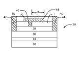
- FIG. 8is a schematic cross-section of a unit cell 30 of a nitride-based HEMT device.
- the device 30includes a substrate 32 , which may comprise silicon carbide, sapphire, spinel, ZnO, silicon or any other material capable of supporting growth of Group III-nitride materials.
- MOCVDMetalorganic Chemical Vapor Deposition
- HVPEHydride Vapor Phase Epitaxy
- MBEMolecular Beam Epitaxy
- a high resistivity Group III-nitride channel layer 36is formed on the nucleation layer 34 .
- Each of the channel layer 36 and barrier layer 38may comprise sub-layers that may comprise doped or undoped layers of Group III-nitride materials. Exemplary structures are illustrated in [3], [9], [10], [11] and [12]. Other nitride-based HEMT structures are illustrated in [13] and [14].
- a Group III-nitride semiconductor spacer layer 40is grown on the Al x Ga 1 ⁇ x N barrier layer 28 .
- Spacer layer 40may have a uniform or graded composition. Spacer layer 40 may be undoped and/or may be designed to be fully depleted as grown.
- Source 42 and drain 44 electrodesare formed making ohmic contacts through the barrier layer 38 such that an electric current flows between the source and drain electrodes 42 , 44 via a two-dimensional electron gas (2DEG) induced at the heterointerface between the channel layer 36 and barrier layer 38 when a gate electrode 46 is biased at an appropriate level.
- 2DEGtwo-dimensional electron gas
- the spacer layer 40may be etched and the gate electrode 46 deposited such that the bottom of the gate electrode 46 is on the surface of barrier layer 38 .
- the metal forming the gate electrode 46may be patterned to extend across spacer layer 40 so that the top of the gate 46 forms a field plate structure 48 extending a distance Lf away from the edge of gate 46 towards drain 44 .
- the part of the gate 46 metal resting on the spacer layer 40forms an epitaxial field plate 48 .
- the structureis covered with a dielectric passivation layer 50 such as silicon nitride. Methods of forming the dielectric passivation 50 are described in detail in the patents and publications referenced above.
- FIG. 9is a schematic cross-section of a unit cell 30 of a nitride-based HEMT device having a different configuration from the device illustrated in FIG. 8 .
- the substrate 32 , nucleation layer 34 , channel layer 36 and barrier layer 38 in the device 30 illustrated in FIG. 9are similar to the corresponding layers illustrated in FIG. 8 .
- the substrate 32comprises semi-insulating 4H—SiC commercially available from Cree, Inc.
- the gate electrode 46is formed after formation of barrier layer 38 and passivation layer 50 is deposited on the device.
- a field plate 48is then formed on the passivation layer 50 overlapping the gate 46 and extending a distance Lf in the gate-drain region.
- passivation layer 50serves as a spacer layer for the field plate 48 .
- the overlap of the field plate 48 above the gate 46 and the amount of extension in the gate-drain regionmay be varied for optimum results.
- Field plate 48 and gate 46may be electrically connected with a via or other connection (not shown).
- the field plate 48may extend a distance Lf of 0.2 to 1 ⁇ m. In some embodiments, the field plate 48 may extend a distance Lf of 0.5 to 0.9 ⁇ m. In preferred embodiments, the field plate 48 may extend a distance Lf of 0.7 ⁇ m.
- a GaN-based HEMT structure in accordance with the embodiment of FIG. 9was constructed and tested.
- the deviceachieved a power density of 32 W/mm with 55% Power Added Efficiency (PAE) operating at 120 V and 4 GHz.
- PAEPower Added Efficiency
- the effect of field plate distance (Lf) on device performancewas tested.
- Deviceswere fabricated generally in accordance with the embodiment of FIG. 9 except that the field plate length Lf was varied from a distance of 0 to 0.9 ⁇ m.
- the PAE of the resulting deviceswas then measured. As illustrated in FIG. 10 , the PAE showed improvement once the field plate length was extended to 0.5 ⁇ m, with an optimum length of about 0.7 ⁇ m. However, the optimum length may depend on the specific device design as well as operating voltage and frequency.
Landscapes
- Engineering & Computer Science (AREA)
- Manufacturing & Machinery (AREA)
- Physics & Mathematics (AREA)
- Condensed Matter Physics & Semiconductors (AREA)
- General Physics & Mathematics (AREA)
- Computer Hardware Design (AREA)
- Microelectronics & Electronic Packaging (AREA)
- Power Engineering (AREA)
- Junction Field-Effect Transistors (AREA)
- Electrodes Of Semiconductors (AREA)
Abstract
Description
Claims (23)
Priority Applications (3)
| Application Number | Priority Date | Filing Date | Title |
|---|---|---|---|
| US10/570,964US7812369B2 (en) | 2003-09-09 | 2004-09-09 | Fabrication of single or multiple gate field plates |
| US12/898,341US9496353B2 (en) | 2003-09-09 | 2010-10-05 | Fabrication of single or multiple gate field plates |
| US15/283,008US10109713B2 (en) | 2003-09-09 | 2016-09-30 | Fabrication of single or multiple gate field plates |
Applications Claiming Priority (3)
| Application Number | Priority Date | Filing Date | Title |
|---|---|---|---|
| US50155703P | 2003-09-09 | 2003-09-09 | |
| US10/570,964US7812369B2 (en) | 2003-09-09 | 2004-09-09 | Fabrication of single or multiple gate field plates |
| PCT/US2004/029324WO2005024909A2 (en) | 2003-09-09 | 2004-09-09 | Fabrication of single or multiple gate field plates |
Related Parent Applications (1)
| Application Number | Title | Priority Date | Filing Date |
|---|---|---|---|
| PCT/US2004/029324A-371-Of-InternationalWO2005024909A2 (en) | 2003-09-09 | 2004-09-09 | Fabrication of single or multiple gate field plates |
Related Child Applications (1)
| Application Number | Title | Priority Date | Filing Date |
|---|---|---|---|
| US12/898,341DivisionUS9496353B2 (en) | 2003-09-09 | 2010-10-05 | Fabrication of single or multiple gate field plates |
Publications (2)
| Publication Number | Publication Date |
|---|---|
| US20070059873A1 US20070059873A1 (en) | 2007-03-15 |
| US7812369B2true US7812369B2 (en) | 2010-10-12 |
Family
ID=34312287
Family Applications (3)
| Application Number | Title | Priority Date | Filing Date |
|---|---|---|---|
| US10/570,964Expired - LifetimeUS7812369B2 (en) | 2003-09-09 | 2004-09-09 | Fabrication of single or multiple gate field plates |
| US12/898,341Expired - LifetimeUS9496353B2 (en) | 2003-09-09 | 2010-10-05 | Fabrication of single or multiple gate field plates |
| US15/283,008Expired - LifetimeUS10109713B2 (en) | 2003-09-09 | 2016-09-30 | Fabrication of single or multiple gate field plates |
Family Applications After (2)
| Application Number | Title | Priority Date | Filing Date |
|---|---|---|---|
| US12/898,341Expired - LifetimeUS9496353B2 (en) | 2003-09-09 | 2010-10-05 | Fabrication of single or multiple gate field plates |
| US15/283,008Expired - LifetimeUS10109713B2 (en) | 2003-09-09 | 2016-09-30 | Fabrication of single or multiple gate field plates |
Country Status (8)
| Country | Link |
|---|---|
| US (3) | US7812369B2 (en) |
| EP (2) | EP2592655B1 (en) |
| JP (3) | JP2007505483A (en) |
| KR (1) | KR101128376B1 (en) |
| CN (1) | CN100541745C (en) |
| CA (1) | CA2538077C (en) |
| TW (3) | TWI430341B (en) |
| WO (1) | WO2005024909A2 (en) |
Cited By (54)
| Publication number | Priority date | Publication date | Assignee | Title |
|---|---|---|---|---|
| US20050253167A1 (en)* | 2004-05-13 | 2005-11-17 | Cree, Inc. | Wide bandgap field effect transistors with source connected field plates |
| US20060202272A1 (en)* | 2005-03-11 | 2006-09-14 | Cree, Inc. | Wide bandgap transistors with gate-source field plates |
| US20090267116A1 (en)* | 2004-05-11 | 2009-10-29 | Cree,Inc. | Wide bandgap transistors with multiple field plates |
| US20110169054A1 (en)* | 2004-05-11 | 2011-07-14 | Cree, Inc. | Wide bandgap hemts with source connected field plates |
| US8237198B2 (en) | 2008-12-10 | 2012-08-07 | Transphorm Inc. | Semiconductor heterostructure diodes |
| US20120223366A1 (en)* | 2006-11-21 | 2012-09-06 | Cree, Inc. | High voltage gan transistor |
| US8289065B2 (en) | 2008-09-23 | 2012-10-16 | Transphorm Inc. | Inductive load power switching circuits |
| US8389977B2 (en) | 2009-12-10 | 2013-03-05 | Transphorm Inc. | Reverse side engineered III-nitride devices |
| US8390000B2 (en) | 2009-08-28 | 2013-03-05 | Transphorm Inc. | Semiconductor devices with field plates |
| US8519438B2 (en) | 2008-04-23 | 2013-08-27 | Transphorm Inc. | Enhancement mode III-N HEMTs |
| US8598937B2 (en) | 2011-10-07 | 2013-12-03 | Transphorm Inc. | High power semiconductor electronic components with increased reliability |
| US8643062B2 (en) | 2011-02-02 | 2014-02-04 | Transphorm Inc. | III-N device structures and methods |
| US8716141B2 (en) | 2011-03-04 | 2014-05-06 | Transphorm Inc. | Electrode configurations for semiconductor devices |
| US8742459B2 (en) | 2009-05-14 | 2014-06-03 | Transphorm Inc. | High voltage III-nitride semiconductor devices |
| US8742460B2 (en) | 2010-12-15 | 2014-06-03 | Transphorm Inc. | Transistors with isolation regions |
| US8772842B2 (en) | 2011-03-04 | 2014-07-08 | Transphorm, Inc. | Semiconductor diodes with low reverse bias currents |
| US8901604B2 (en) | 2011-09-06 | 2014-12-02 | Transphorm Inc. | Semiconductor devices with guard rings |
| WO2014200753A2 (en) | 2013-06-09 | 2014-12-18 | Cree, Inc. | Recessed field plate transistor structures |
| WO2014200820A1 (en) | 2013-06-09 | 2014-12-18 | Cree, Inc | Cascode structures with gan cap layers |
| US8933486B2 (en) | 2006-11-13 | 2015-01-13 | Cree, Inc. | GaN based HEMTs with buried field plates |
| US9093366B2 (en) | 2012-04-09 | 2015-07-28 | Transphorm Inc. | N-polar III-nitride transistors |
| US9165766B2 (en) | 2012-02-03 | 2015-10-20 | Transphorm Inc. | Buffer layer structures suited for III-nitride devices with foreign substrates |
| US9171730B2 (en) | 2013-02-15 | 2015-10-27 | Transphorm Inc. | Electrodes for semiconductor devices and methods of forming the same |
| US9184275B2 (en) | 2012-06-27 | 2015-11-10 | Transphorm Inc. | Semiconductor devices with integrated hole collectors |
| US9245993B2 (en) | 2013-03-15 | 2016-01-26 | Transphorm Inc. | Carbon doping semiconductor devices |
| US9257547B2 (en) | 2011-09-13 | 2016-02-09 | Transphorm Inc. | III-N device structures having a non-insulating substrate |
| US9318593B2 (en) | 2014-07-21 | 2016-04-19 | Transphorm Inc. | Forming enhancement mode III-nitride devices |
| US9397173B2 (en) | 2003-09-09 | 2016-07-19 | Cree, Inc. | Wide bandgap transistor devices with field plates |
| US9443938B2 (en) | 2013-07-19 | 2016-09-13 | Transphorm Inc. | III-nitride transistor including a p-type depleting layer |
| US9536967B2 (en) | 2014-12-16 | 2017-01-03 | Transphorm Inc. | Recessed ohmic contacts in a III-N device |
| US9536966B2 (en) | 2014-12-16 | 2017-01-03 | Transphorm Inc. | Gate structures for III-N devices |
| US20170025506A1 (en)* | 2003-09-09 | 2017-01-26 | The Regents Of The University Of California | Fabrication of single or multiple gate field plates |
| US9590060B2 (en) | 2013-03-13 | 2017-03-07 | Transphorm Inc. | Enhancement-mode III-nitride devices |
| US9679981B2 (en) | 2013-06-09 | 2017-06-13 | Cree, Inc. | Cascode structures for GaN HEMTs |
| US20190006498A1 (en)* | 2015-11-06 | 2019-01-03 | Taiwan Semiconductor Manufacturing Company Ltd. | High-electron-mobility transistor and manufacturing method thereof |
| US10192980B2 (en) | 2016-06-24 | 2019-01-29 | Cree, Inc. | Gallium nitride high-electron mobility transistors with deep implanted p-type layers in silicon carbide substrates for power switching and radio frequency applications and process for making the same |
| US10224401B2 (en) | 2016-05-31 | 2019-03-05 | Transphorm Inc. | III-nitride devices including a graded depleting layer |
| US10354879B2 (en) | 2016-06-24 | 2019-07-16 | Cree, Inc. | Depletion mode semiconductor devices including current dependent resistance |
| US10840334B2 (en) | 2016-06-24 | 2020-11-17 | Cree, Inc. | Gallium nitride high-electron mobility transistors with deep implanted p-type layers in silicon carbide substrates for power switching and radio frequency applications and process for making the same |
| US10892356B2 (en) | 2016-06-24 | 2021-01-12 | Cree, Inc. | Group III-nitride high-electron mobility transistors with buried p-type layers and process for making the same |
| US11004952B1 (en) | 2019-11-05 | 2021-05-11 | United Microelectronics Corp. | High-electron mobility transistor and fabrication method thereof |
| WO2021146229A1 (en) | 2020-01-14 | 2021-07-22 | Cree, Inc. | Group iii hemt and capacitor that share structural features |
| US11088271B2 (en) | 2019-10-30 | 2021-08-10 | United Microelectronics Corp. | High electron mobility transistor and method for fabricating the same |
| WO2021257853A1 (en) | 2020-06-17 | 2021-12-23 | Cree, Inc. | Multi-stage decoupling networks integrated with on-package impedance matching networks for rf power amplifiers |
| US11316019B2 (en) | 2020-07-29 | 2022-04-26 | Globalfoundries U.S. Inc. | Symmetric arrangement of field plates in semiconductor devices |
| US11322599B2 (en) | 2016-01-15 | 2022-05-03 | Transphorm Technology, Inc. | Enhancement mode III-nitride devices having an Al1-xSixO gate insulator |
| US11430882B2 (en) | 2016-06-24 | 2022-08-30 | Wolfspeed, Inc. | Gallium nitride high-electron mobility transistors with p-type layers and process for making the same |
| US11929428B2 (en) | 2021-05-17 | 2024-03-12 | Wolfspeed, Inc. | Circuits and group III-nitride high-electron mobility transistors with buried p-type layers improving overload recovery and process for implementing the same |
| US12148820B2 (en) | 2021-12-20 | 2024-11-19 | Nxp B.V. | Transistors with source-connected field plates |
| US12230699B2 (en) | 2019-10-23 | 2025-02-18 | Analog Devices, Inc. | Modification of electric fields of compound semiconductor devices |
| US12342560B2 (en) | 2021-12-20 | 2025-06-24 | Nxp Usa, Inc. | Transistors with source-connected field plates |
| US12349433B2 (en) | 2021-12-20 | 2025-07-01 | Nxp Usa, Inc. | Transistors with self-aligned source-connected field plates |
| US12402341B2 (en) | 2022-03-11 | 2025-08-26 | Sumitomo Electric Industries, Ltd. | Method for manufacturing semiconductor device |
| US12402346B2 (en) | 2021-05-17 | 2025-08-26 | Wolfspeed, Inc. | Circuits and group III-nitride transistors with buried p-layers and controlled gate voltages and methods thereof |
Families Citing this family (33)
| Publication number | Priority date | Publication date | Assignee | Title |
|---|---|---|---|---|
| US7612390B2 (en) | 2004-02-05 | 2009-11-03 | Cree, Inc. | Heterojunction transistors including energy barriers |
| US20050218414A1 (en)* | 2004-03-30 | 2005-10-06 | Tetsuzo Ueda | 4H-polytype gallium nitride-based semiconductor device on a 4H-polytype substrate |
| US7161194B2 (en) | 2004-12-06 | 2007-01-09 | Cree, Inc. | High power density and/or linearity transistors |
| JP2006286698A (en)* | 2005-03-31 | 2006-10-19 | Furukawa Electric Co Ltd:The | Electronic device and power converter |
| US20060223293A1 (en)* | 2005-04-01 | 2006-10-05 | Raytheon Company | Semiconductor devices having improved field plates |
| JP4968068B2 (en) | 2005-06-10 | 2012-07-04 | 日本電気株式会社 | Field effect transistor |
| EP1901341A4 (en)* | 2005-06-10 | 2009-07-15 | Nec Corp | FIELD EFFECT TRANSISTOR |
| US8114717B2 (en)* | 2005-11-15 | 2012-02-14 | The Regents Of The University Of California | Methods to shape the electric field in electron devices, passivate dislocations and point defects, and enhance the luminescence efficiency of optical devices |
| US7592211B2 (en) | 2006-01-17 | 2009-09-22 | Cree, Inc. | Methods of fabricating transistors including supported gate electrodes |
| US7566918B2 (en) | 2006-02-23 | 2009-07-28 | Cree, Inc. | Nitride based transistors for millimeter wave operation |
| US7388236B2 (en) | 2006-03-29 | 2008-06-17 | Cree, Inc. | High efficiency and/or high power density wide bandgap transistors |
| JP5217151B2 (en)* | 2006-08-25 | 2013-06-19 | 日亜化学工業株式会社 | Field effect transistor and manufacturing method thereof |
| KR100782430B1 (en)* | 2006-09-22 | 2007-12-05 | 한국과학기술원 | Gallium Nitride based high electron mobility transistor structure with internal field electrodes for high power |
| US7501670B2 (en)* | 2007-03-20 | 2009-03-10 | Velox Semiconductor Corporation | Cascode circuit employing a depletion-mode, GaN-based FET |
| WO2009116015A1 (en)* | 2008-03-20 | 2009-09-24 | Nxp B.V. | Finfet transistor with high-voltage capability and cmos-compatible method for fabricating the same |
| JP5499441B2 (en)* | 2008-04-01 | 2014-05-21 | 沖電気工業株式会社 | Semiconductor device and manufacturing method thereof |
| US8829999B2 (en) | 2010-05-20 | 2014-09-09 | Cree, Inc. | Low noise amplifiers including group III nitride based high electron mobility transistors |
| CN102201442B (en)* | 2011-04-02 | 2014-06-18 | 中国科学院苏州纳米技术与纳米仿生研究所 | Heterojunction field effect transistor based on channel array structure |
| WO2014050054A1 (en)* | 2012-09-28 | 2014-04-03 | パナソニック株式会社 | Semiconductor device |
| JP2014165280A (en)* | 2013-02-22 | 2014-09-08 | Toshiba Corp | Semiconductor device |
| US9407214B2 (en) | 2013-06-28 | 2016-08-02 | Cree, Inc. | MMIC power amplifier |
| US20150171860A1 (en)* | 2013-11-13 | 2015-06-18 | Skyworks Solutions, Inc. | Circuits and methods for improved quality factor in a stack of transistors |
| US9093394B1 (en)* | 2013-12-16 | 2015-07-28 | Hrl Laboratories, Llc | Method and structure for encapsulation and interconnection of transistors |
| JP2015195288A (en)* | 2014-03-31 | 2015-11-05 | 住友電工デバイス・イノベーション株式会社 | Semiconductor device and semiconductor device manufacturing method |
| CN104332498B (en)* | 2014-09-01 | 2018-01-05 | 苏州捷芯威半导体有限公司 | A kind of tiltedly preparation method of field plate power device and oblique field plate power device |
| US9722063B1 (en)* | 2016-04-11 | 2017-08-01 | Power Integrations, Inc. | Protective insulator for HFET devices |
| KR20180068172A (en)* | 2016-12-13 | 2018-06-21 | (주)웨이비스 | A HEMT and manufacturing method thereof |
| CN107170797B (en)* | 2017-03-29 | 2020-04-14 | 西安电子科技大学 | Drainage field plate-based current aperture heterojunction transistor and fabrication method thereof |
| FR3105580A1 (en)* | 2019-12-20 | 2021-06-25 | Thales | IMPROVED HEMT TRANSISTOR |
| US11424356B2 (en) | 2020-03-16 | 2022-08-23 | Raytheon Company | Transistor having resistive field plate |
| US12408403B2 (en)* | 2020-10-27 | 2025-09-02 | Macom Technology Solutions Holdings, Inc. | Field effect transistor with stacked unit subcell structure |
| US12191383B2 (en) | 2021-12-24 | 2025-01-07 | Nxp Usa, Inc. | Semiconductor device with an insulating region formed between a control electrode and a conductive element and method of fabrication therefor |
| WO2025059208A1 (en)* | 2023-09-13 | 2025-03-20 | Soctera, Inc. | Current collapse reduction using aluminum nitride back barrier and in-situ two-step passivation |
Citations (24)
| Publication number | Priority date | Publication date | Assignee | Title |
|---|---|---|---|---|
| US4999682A (en) | 1987-08-14 | 1991-03-12 | Regents Of The University Of Minnesota | Electronic and optoelectronic laser devices utilizing light hole properties |
| US5192987A (en) | 1991-05-17 | 1993-03-09 | Apa Optics, Inc. | High electron mobility transistor with GaN/Alx Ga1-x N heterojunctions |
| US5290393A (en) | 1991-01-31 | 1994-03-01 | Nichia Kagaku Kogyo K.K. | Crystal growth method for gallium nitride-based compound semiconductor |
| US5393993A (en) | 1993-12-13 | 1995-02-28 | Cree Research, Inc. | Buffer structure between silicon carbide and gallium nitride and resulting semiconductor devices |
| US5523589A (en) | 1994-09-20 | 1996-06-04 | Cree Research, Inc. | Vertical geometry light emitting diode with group III nitride active layer and extended lifetime |
| US5686738A (en) | 1991-03-18 | 1997-11-11 | Trustees Of Boston University | Highly insulating monocrystalline gallium nitride thin films |
| US5739554A (en) | 1995-05-08 | 1998-04-14 | Cree Research, Inc. | Double heterojunction light emitting diode with gallium nitride active layer |
| US6294801B1 (en)* | 1998-05-01 | 2001-09-25 | Oki Electric Industry Co., Ltd. | Semiconductor device with Schottky layer |
| US6316793B1 (en) | 1998-06-12 | 2001-11-13 | Cree, Inc. | Nitride based transistors on semi-insulating silicon carbide substrates |
| US6316820B1 (en)* | 1997-07-25 | 2001-11-13 | Hughes Electronics Corporation | Passivation layer and process for semiconductor devices |
| US20020005528A1 (en)* | 2000-07-17 | 2002-01-17 | Fujitsu Quantum Devices Limited | High-speed compound semiconductor device operable at large output power with minimum leakage current |
| US6445038B1 (en) | 1998-01-09 | 2002-09-03 | Infineon Technologies Ag | Silicon on insulator high-voltage switch |
| US20020145172A1 (en) | 2001-03-12 | 2002-10-10 | Naoto Fujishima | High withstand voltage semiconductor device |
| US6465814B2 (en)* | 2000-06-29 | 2002-10-15 | Nec Corporation | Semiconductor device |
| US20020167023A1 (en) | 2001-05-11 | 2002-11-14 | Cree Lighting Company And Regents Of The University Of California | Group-III nitride based high electron mobility transistor (HEMT) with barrier/spacer layer |
| US20020171096A1 (en) | 2001-05-17 | 2002-11-21 | Nec Corporation | Schottky gate field effect transistor with high output characteristic |
| US20030006437A1 (en) | 1998-09-22 | 2003-01-09 | Nec Corporation | Field effect transistor |
| US20030020092A1 (en) | 2001-07-24 | 2003-01-30 | Primit Parikh | Insulating gate AlGaN/GaN HEMT |
| US6548333B2 (en) | 2000-12-01 | 2003-04-15 | Cree, Inc. | Aluminum gallium nitride/gallium nitride high electron mobility transistors having a gate contact on a gallium nitride based cap segment |
| US20030102482A1 (en) | 2001-12-03 | 2003-06-05 | Saxler Adam William | Strain balanced nitride heterojunction transistors and methods of fabricating strain balanced nitride heterojunction transistors |
| WO2003050849A2 (en) | 2001-12-06 | 2003-06-19 | Hrl Laboratories, Llc | High power-low noise microwave gan heterojunction field effet transistor |
| US6586781B2 (en) | 2000-02-04 | 2003-07-01 | Cree Lighting Company | Group III nitride based FETs and HEMTs with reduced trapping and method for producing the same |
| US20030136986A1 (en)* | 2001-12-07 | 2003-07-24 | Elmasry Nadia A. | Transition metal doped ferromagnetic III-V nitride material films and methods of fabricating the same |
| US7126426B2 (en)* | 2003-09-09 | 2006-10-24 | Cree, Inc. | Cascode amplifier structures including wide bandgap field effect transistor with field plates |
Family Cites Families (44)
| Publication number | Priority date | Publication date | Assignee | Title |
|---|---|---|---|---|
| BE401036A (en) | 1933-06-27 | |||
| JPS5893377A (en) | 1981-11-30 | 1983-06-03 | Fujitsu Ltd | Semiconductor device |
| JPH04162633A (en) | 1990-10-26 | 1992-06-08 | Fuji Xerox Co Ltd | Thin film transistor |
| JP3135939B2 (en)* | 1991-06-20 | 2001-02-19 | 富士通株式会社 | HEMT type semiconductor device |
| JPH05326563A (en)* | 1992-05-21 | 1993-12-10 | Toshiba Corp | Semiconductor device |
| JPH06124965A (en) | 1992-10-09 | 1994-05-06 | Sumitomo Electric Ind Ltd | Field effect transistor |
| JPH06163600A (en) | 1992-11-26 | 1994-06-10 | Nec Corp | Field-effect transistor |
| US6002148A (en)* | 1995-06-30 | 1999-12-14 | Motorola, Inc. | Silicon carbide transistor and method |
| KR0167273B1 (en) | 1995-12-02 | 1998-12-15 | 문정환 | High voltage mosfet device and manufacturing method thereof |
| JPH09232827A (en)* | 1996-02-21 | 1997-09-05 | Oki Electric Ind Co Ltd | Semiconductor device and transmission / reception switching type antenna switch circuit |
| JP3616447B2 (en)* | 1996-02-27 | 2005-02-02 | 富士通株式会社 | Semiconductor device |
| TW373247B (en) | 1998-04-02 | 1999-11-01 | Taiwan Semiconductor Mfg Co Ltd | Contact face having uplift and delay S/D and stock silicon gate electrode P type gold oxygen semi-field effect transistor forming method |
| US6009023A (en) | 1998-05-26 | 1999-12-28 | Etron Technology, Inc. | High performance DRAM structure employing multiple thickness gate oxide |
| JP3111985B2 (en)* | 1998-06-16 | 2000-11-27 | 日本電気株式会社 | Field-effect transistor |
| JP2000082671A (en) | 1998-06-26 | 2000-03-21 | Sony Corp | Nitride based iii-v compound semiconductor device and its manufacture |
| JP3271613B2 (en)* | 1999-05-06 | 2002-04-02 | 日本電気株式会社 | Field effect transistor |
| TW517260B (en) | 1999-05-15 | 2003-01-11 | Semiconductor Energy Lab | Semiconductor device and method for its fabrication |
| JP2001085670A (en) | 1999-09-14 | 2001-03-30 | Nec Corp | Field effect transistor and method of manufacturing the same |
| US6774449B1 (en) | 1999-09-16 | 2004-08-10 | Matsushita Electric Industrial Co., Ltd. | Semiconductor device and method for fabricating the same |
| JP3344416B2 (en) | 1999-09-16 | 2002-11-11 | 松下電器産業株式会社 | Semiconductor device and method of manufacturing the same |
| US6639255B2 (en)* | 1999-12-08 | 2003-10-28 | Matsushita Electric Industrial Co., Ltd. | GaN-based HFET having a surface-leakage reducing cap layer |
| JP4592938B2 (en) | 1999-12-08 | 2010-12-08 | パナソニック株式会社 | Semiconductor device |
| JP2001237250A (en)* | 2000-02-22 | 2001-08-31 | Nec Corp | Semiconductor device |
| JP2001326335A (en)* | 2000-05-18 | 2001-11-22 | Nec Corp | Field effect transistor |
| JP4198339B2 (en) | 2000-07-17 | 2008-12-17 | ユーディナデバイス株式会社 | Compound semiconductor device |
| US6690042B2 (en)* | 2000-09-27 | 2004-02-10 | Sensor Electronic Technology, Inc. | Metal oxide semiconductor heterostructure field effect transistor |
| JP2002118122A (en)* | 2000-10-06 | 2002-04-19 | Nec Corp | Schottky gate field effect transistor |
| TW466747B (en) | 2000-12-14 | 2001-12-01 | United Microelectronics Corp | Using inner field ring and complex multiple field plates to reduce surface breakdown of power LDMOSFET |
| JP2001230263A (en)* | 2001-01-29 | 2001-08-24 | Nec Corp | Field effect transistor |
| JP4220683B2 (en) | 2001-03-27 | 2009-02-04 | パナソニック株式会社 | Semiconductor device |
| JP2003059948A (en) | 2001-08-20 | 2003-02-28 | Sanken Electric Co Ltd | Semiconductor device and production method therefor |
| JP2003100778A (en) | 2001-09-26 | 2003-04-04 | Toshiba Corp | Semiconductor device |
| TW511190B (en) | 2001-11-09 | 2002-11-21 | Macronix Int Co Ltd | Non-volatile semiconductor memory device with multi-layer gate insulating structure |
| JP4117535B2 (en)* | 2001-11-30 | 2008-07-16 | 信越半導体株式会社 | Compound semiconductor device |
| JP3705431B2 (en)* | 2002-03-28 | 2005-10-12 | ユーディナデバイス株式会社 | Semiconductor device and manufacturing method thereof |
| US6559513B1 (en)* | 2002-04-22 | 2003-05-06 | M/A-Com, Inc. | Field-plate MESFET |
| US6893947B2 (en)* | 2002-06-25 | 2005-05-17 | Freescale Semiconductor, Inc. | Advanced RF enhancement-mode FETs with improved gate properties |
| JP3790500B2 (en)* | 2002-07-16 | 2006-06-28 | ユーディナデバイス株式会社 | Field effect transistor and manufacturing method thereof |
| US6740535B2 (en) | 2002-07-29 | 2004-05-25 | International Business Machines Corporation | Enhanced T-gate structure for modulation doped field effect transistors |
| US6933544B2 (en) | 2003-01-29 | 2005-08-23 | Kabushiki Kaisha Toshiba | Power semiconductor device |
| US7812369B2 (en)* | 2003-09-09 | 2010-10-12 | The Regents Of The University Of California | Fabrication of single or multiple gate field plates |
| US7501669B2 (en)* | 2003-09-09 | 2009-03-10 | Cree, Inc. | Wide bandgap transistor devices with field plates |
| US7573078B2 (en)* | 2004-05-11 | 2009-08-11 | Cree, Inc. | Wide bandgap transistors with multiple field plates |
| US7692263B2 (en)* | 2006-11-21 | 2010-04-06 | Cree, Inc. | High voltage GaN transistors |
- 2004
- 2004-09-09USUS10/570,964patent/US7812369B2/ennot_activeExpired - Lifetime
- 2004-09-09EPEP12192425.2Apatent/EP2592655B1/ennot_activeExpired - Lifetime
- 2004-09-09WOPCT/US2004/029324patent/WO2005024909A2/enactiveApplication Filing
- 2004-09-09TWTW093127327Apatent/TWI430341B/ennot_activeIP Right Cessation
- 2004-09-09JPJP2006525544Apatent/JP2007505483A/enactivePending
- 2004-09-09CNCNB2004800259769Apatent/CN100541745C/ennot_activeExpired - Lifetime
- 2004-09-09TWTW100142118Apatent/TWI431674B/ennot_activeIP Right Cessation
- 2004-09-09KRKR1020067004893Apatent/KR101128376B1/ennot_activeExpired - Lifetime
- 2004-09-09EPEP04788636.1Apatent/EP1665358B1/ennot_activeExpired - Lifetime
- 2004-09-09TWTW103103844Apatent/TWI560783B/ennot_activeIP Right Cessation
- 2004-09-09CACA2538077Apatent/CA2538077C/ennot_activeExpired - Lifetime
- 2010
- 2010-10-05USUS12/898,341patent/US9496353B2/ennot_activeExpired - Lifetime
- 2011
- 2011-10-19JPJP2011229873Apatent/JP2012044207A/ennot_activeWithdrawn
- 2012
- 2012-03-30JPJP2012081726Apatent/JP2012164994A/ennot_activeWithdrawn
- 2016
- 2016-09-30USUS15/283,008patent/US10109713B2/ennot_activeExpired - Lifetime
Patent Citations (26)
| Publication number | Priority date | Publication date | Assignee | Title |
|---|---|---|---|---|
| US4999682A (en) | 1987-08-14 | 1991-03-12 | Regents Of The University Of Minnesota | Electronic and optoelectronic laser devices utilizing light hole properties |
| US5290393A (en) | 1991-01-31 | 1994-03-01 | Nichia Kagaku Kogyo K.K. | Crystal growth method for gallium nitride-based compound semiconductor |
| US5686738A (en) | 1991-03-18 | 1997-11-11 | Trustees Of Boston University | Highly insulating monocrystalline gallium nitride thin films |
| US5192987A (en) | 1991-05-17 | 1993-03-09 | Apa Optics, Inc. | High electron mobility transistor with GaN/Alx Ga1-x N heterojunctions |
| US5296395A (en) | 1991-05-17 | 1994-03-22 | Apa Optics, Inc. | Method of making a high electron mobility transistor |
| US5393993A (en) | 1993-12-13 | 1995-02-28 | Cree Research, Inc. | Buffer structure between silicon carbide and gallium nitride and resulting semiconductor devices |
| US5523589A (en) | 1994-09-20 | 1996-06-04 | Cree Research, Inc. | Vertical geometry light emitting diode with group III nitride active layer and extended lifetime |
| US5739554A (en) | 1995-05-08 | 1998-04-14 | Cree Research, Inc. | Double heterojunction light emitting diode with gallium nitride active layer |
| US6316820B1 (en)* | 1997-07-25 | 2001-11-13 | Hughes Electronics Corporation | Passivation layer and process for semiconductor devices |
| US6445038B1 (en) | 1998-01-09 | 2002-09-03 | Infineon Technologies Ag | Silicon on insulator high-voltage switch |
| US6294801B1 (en)* | 1998-05-01 | 2001-09-25 | Oki Electric Industry Co., Ltd. | Semiconductor device with Schottky layer |
| US6316793B1 (en) | 1998-06-12 | 2001-11-13 | Cree, Inc. | Nitride based transistors on semi-insulating silicon carbide substrates |
| US20030006437A1 (en) | 1998-09-22 | 2003-01-09 | Nec Corporation | Field effect transistor |
| US6586781B2 (en) | 2000-02-04 | 2003-07-01 | Cree Lighting Company | Group III nitride based FETs and HEMTs with reduced trapping and method for producing the same |
| US6465814B2 (en)* | 2000-06-29 | 2002-10-15 | Nec Corporation | Semiconductor device |
| US6586813B2 (en) | 2000-07-17 | 2003-07-01 | Fujitsu Quantum Devices Limited | High-speed compound semiconductor device operable at large output power with minimum leakage current |
| US20020005528A1 (en)* | 2000-07-17 | 2002-01-17 | Fujitsu Quantum Devices Limited | High-speed compound semiconductor device operable at large output power with minimum leakage current |
| US6548333B2 (en) | 2000-12-01 | 2003-04-15 | Cree, Inc. | Aluminum gallium nitride/gallium nitride high electron mobility transistors having a gate contact on a gallium nitride based cap segment |
| US20020145172A1 (en) | 2001-03-12 | 2002-10-10 | Naoto Fujishima | High withstand voltage semiconductor device |
| US20020167023A1 (en) | 2001-05-11 | 2002-11-14 | Cree Lighting Company And Regents Of The University Of California | Group-III nitride based high electron mobility transistor (HEMT) with barrier/spacer layer |
| US20020171096A1 (en) | 2001-05-17 | 2002-11-21 | Nec Corporation | Schottky gate field effect transistor with high output characteristic |
| US20030020092A1 (en) | 2001-07-24 | 2003-01-30 | Primit Parikh | Insulating gate AlGaN/GaN HEMT |
| US20030102482A1 (en) | 2001-12-03 | 2003-06-05 | Saxler Adam William | Strain balanced nitride heterojunction transistors and methods of fabricating strain balanced nitride heterojunction transistors |
| WO2003050849A2 (en) | 2001-12-06 | 2003-06-19 | Hrl Laboratories, Llc | High power-low noise microwave gan heterojunction field effet transistor |
| US20030136986A1 (en)* | 2001-12-07 | 2003-07-24 | Elmasry Nadia A. | Transition metal doped ferromagnetic III-V nitride material films and methods of fabricating the same |
| US7126426B2 (en)* | 2003-09-09 | 2006-10-24 | Cree, Inc. | Cascode amplifier structures including wide bandgap field effect transistor with field plates |
Non-Patent Citations (19)
| Title |
|---|
| A.T. Ping et al., "DC and Microwave Performance of High-Current AlGaN/GaN Heterostructure Field Effect Transistors Grown on p-Type Sic Substrates",IEEE Electron Device Letters, vol. 19, No. 2, Feb. 1998, pp. 54-56. |
| B. Gelmont et al., "Monte Carlo Simulation of Electron Transport in Gallium Nitride", 1983 American Institute of Physics, vol. 74, No. 3, pp. 1818-1821. |
| Chinese Office Action issued May 16, 2008, Application No. 200480025976.9. |
| G.J. Sullivan et al., "High-power 10 GHz Operation of AlGaN HFET's on Insulating SiC", IEEE Electron Device Letters, vol. 19, No. 6, Jun. 1998. |
| K. Asano et al., "Novel High Power AlGaAs/GaAs HFET with a Field-Modulating Plate Operated at 35V Drain Voltage", 1998 International Electron Devices Meeting, Technical Digest, pp. 3.3.1-3.3.4. |
| Lester F. Eastman et al., "GaN Materials for High Power Microwave Amplifiers", Mnt, Res. Soc. Symp. Proc. vol. 512, 1996 Materials Research Society. |
| Li, "High breakdown voltage GaN HFET with field plate," Electronic Letters, Feb. 1, 2001, vol. 37, No. 3, pp. 196-197. |
| Miroslav Micovic et al, "AlGaN/GaN Heterojunction Field Effect Transistors Grown by Nitrogen Plasma Assisted Molecular Beam Epitaxy", IEEE Transactions on Electron Devices, vol. 48, No. 3, Mar. 2001, pp. 591-596. |
| R. Gaska et al., "Electron transport in AlGaN-GaN heterostructures grown on 6H-SiC substrates", 1998 American Institute of Physics, vol. 72, No. 6, pp. 707-709. |
| R. Gaska et al., "High-Temperature Performance of AlGaN/GaN HFET's on SiC Substrates", IEEE Electron Device Leters, vol. 18, No. 10, Oct. 1997, pp. 492-494. |
| Richard C. Dorf, "The Electrical Engineering Handbook", Second Edition, CRC Press, IEEE Press, 1997. |
| Shreepad Karmalkar et al., "Very high voltage AlGaN/GaN high electron mobility transistors using a field plate deposited on a stepped insulator", 2001 Elsevier Science Ltd., Solid-State Electronics 45 (2001) pp. 1645-1652. |
| Wataru Saito et al., "600V AlGaN/GaN Power-HEMT: Design, Fabrication and Demonstration on High Voltage DC-DC Converter", IEDM 03-587, 2003 IEEE, pp. 23.7.1-23.7.4. |
| Wu et al., "30-W/mm GaN HEMTs by Field Plate Optimization", IEEE Electron Device Letters, vol. 25, No. 3, 2004. |
| Wu et al., "High-gain Microwave GaN HEMTs with Source-terminated Field-plates", Cree Santa Barbara Technology Center, Goleta, CA. |
| Y. Ando et al., "10-W/mm AlGaN-GaN HFET With a Field Modulating Plate", IEEE Electron Device Letters, vol. 24, No. 5, pp. 289-292, May 2003. |
| Y.-F. Wu et al., "High Al-Content AlGaN/GaN MODFET's for Ultrahigh Performance", IEEE Electron Device Letters, vol. 19, No. 2, Feb. 1998, pp. 50-53. |
| Yi-Feng Wu et al., "GaN-Based FETs for Microwave Power Amplification", IEICE Trans. Electron., vol. E82-C, No. 11, Nov. 1999, pp. 1895-1905. |
| Yi-Feng Wu et al., "Very-High Power Density AlGaN/GaN HEMTs", IEEE Transactions on Electronic Devices, vol. 48, No. 3, Mar. 2001, pp. 586-590. |
Cited By (109)
| Publication number | Priority date | Publication date | Assignee | Title |
|---|---|---|---|---|
| US10109713B2 (en)* | 2003-09-09 | 2018-10-23 | The Regents Of The University Of California | Fabrication of single or multiple gate field plates |
| US20170025506A1 (en)* | 2003-09-09 | 2017-01-26 | The Regents Of The University Of California | Fabrication of single or multiple gate field plates |
| US9397173B2 (en) | 2003-09-09 | 2016-07-19 | Cree, Inc. | Wide bandgap transistor devices with field plates |
| US20110169054A1 (en)* | 2004-05-11 | 2011-07-14 | Cree, Inc. | Wide bandgap hemts with source connected field plates |
| US8664695B2 (en)* | 2004-05-11 | 2014-03-04 | Cree, Inc. | Wide bandgap transistors with multiple field plates |
| US20090267116A1 (en)* | 2004-05-11 | 2009-10-29 | Cree,Inc. | Wide bandgap transistors with multiple field plates |
| US8592867B2 (en) | 2004-05-11 | 2013-11-26 | Cree, Inc. | Wide bandgap HEMTS with source connected field plates |
| US9773877B2 (en) | 2004-05-13 | 2017-09-26 | Cree, Inc. | Wide bandgap field effect transistors with source connected field plates |
| US20050253167A1 (en)* | 2004-05-13 | 2005-11-17 | Cree, Inc. | Wide bandgap field effect transistors with source connected field plates |
| US11791385B2 (en) | 2005-03-11 | 2023-10-17 | Wolfspeed, Inc. | Wide bandgap transistors with gate-source field plates |
| US20060202272A1 (en)* | 2005-03-11 | 2006-09-14 | Cree, Inc. | Wide bandgap transistors with gate-source field plates |
| US8933486B2 (en) | 2006-11-13 | 2015-01-13 | Cree, Inc. | GaN based HEMTs with buried field plates |
| US20120223366A1 (en)* | 2006-11-21 | 2012-09-06 | Cree, Inc. | High voltage gan transistor |
| US9041064B2 (en)* | 2006-11-21 | 2015-05-26 | Cree, Inc. | High voltage GaN transistor |
| US9450081B2 (en) | 2006-11-21 | 2016-09-20 | Cree, Inc. | High voltage GaN transistor |
| US8519438B2 (en) | 2008-04-23 | 2013-08-27 | Transphorm Inc. | Enhancement mode III-N HEMTs |
| US8841702B2 (en) | 2008-04-23 | 2014-09-23 | Transphorm Inc. | Enhancement mode III-N HEMTs |
| US9941399B2 (en) | 2008-04-23 | 2018-04-10 | Transphorm Inc. | Enhancement mode III-N HEMTs |
| US9196716B2 (en) | 2008-04-23 | 2015-11-24 | Transphorm Inc. | Enhancement mode III-N HEMTs |
| US9437708B2 (en) | 2008-04-23 | 2016-09-06 | Transphorm Inc. | Enhancement mode III-N HEMTs |
| US8493129B2 (en) | 2008-09-23 | 2013-07-23 | Transphorm Inc. | Inductive load power switching circuits |
| US8531232B2 (en) | 2008-09-23 | 2013-09-10 | Transphorm Inc. | Inductive load power switching circuits |
| US8816751B2 (en) | 2008-09-23 | 2014-08-26 | Transphorm Inc. | Inductive load power switching circuits |
| US8289065B2 (en) | 2008-09-23 | 2012-10-16 | Transphorm Inc. | Inductive load power switching circuits |
| US9690314B2 (en) | 2008-09-23 | 2017-06-27 | Transphorm Inc. | Inductive load power switching circuits |
| US9041065B2 (en) | 2008-12-10 | 2015-05-26 | Transphorm Inc. | Semiconductor heterostructure diodes |
| US8541818B2 (en) | 2008-12-10 | 2013-09-24 | Transphorm Inc. | Semiconductor heterostructure diodes |
| US8237198B2 (en) | 2008-12-10 | 2012-08-07 | Transphorm Inc. | Semiconductor heterostructure diodes |
| US8742459B2 (en) | 2009-05-14 | 2014-06-03 | Transphorm Inc. | High voltage III-nitride semiconductor devices |
| US9293561B2 (en) | 2009-05-14 | 2016-03-22 | Transphorm Inc. | High voltage III-nitride semiconductor devices |
| US9373699B2 (en) | 2009-08-28 | 2016-06-21 | Transphorm Inc. | Semiconductor devices with field plates |
| US8390000B2 (en) | 2009-08-28 | 2013-03-05 | Transphorm Inc. | Semiconductor devices with field plates |
| US8692294B2 (en) | 2009-08-28 | 2014-04-08 | Transphorm Inc. | Semiconductor devices with field plates |
| US9831315B2 (en) | 2009-08-28 | 2017-11-28 | Transphorm Inc. | Semiconductor devices with field plates |
| US9111961B2 (en) | 2009-08-28 | 2015-08-18 | Transphorm Inc. | Semiconductor devices with field plates |
| US8389977B2 (en) | 2009-12-10 | 2013-03-05 | Transphorm Inc. | Reverse side engineered III-nitride devices |
| US10199217B2 (en) | 2009-12-10 | 2019-02-05 | Transphorm Inc. | Methods of forming reverse side engineered III-nitride devices |
| US9496137B2 (en) | 2009-12-10 | 2016-11-15 | Transphorm Inc. | Methods of forming reverse side engineered III-nitride devices |
| US9147760B2 (en) | 2010-12-15 | 2015-09-29 | Transphorm Inc. | Transistors with isolation regions |
| US9437707B2 (en) | 2010-12-15 | 2016-09-06 | Transphorm Inc. | Transistors with isolation regions |
| US8742460B2 (en) | 2010-12-15 | 2014-06-03 | Transphorm Inc. | Transistors with isolation regions |
| US8643062B2 (en) | 2011-02-02 | 2014-02-04 | Transphorm Inc. | III-N device structures and methods |
| US9224671B2 (en) | 2011-02-02 | 2015-12-29 | Transphorm Inc. | III-N device structures and methods |
| US8895421B2 (en) | 2011-02-02 | 2014-11-25 | Transphorm Inc. | III-N device structures and methods |
| US8716141B2 (en) | 2011-03-04 | 2014-05-06 | Transphorm Inc. | Electrode configurations for semiconductor devices |
| US9142659B2 (en) | 2011-03-04 | 2015-09-22 | Transphorm Inc. | Electrode configurations for semiconductor devices |
| US8895423B2 (en) | 2011-03-04 | 2014-11-25 | Transphorm Inc. | Method for making semiconductor diodes with low reverse bias currents |
| US8772842B2 (en) | 2011-03-04 | 2014-07-08 | Transphorm, Inc. | Semiconductor diodes with low reverse bias currents |
| US9224805B2 (en) | 2011-09-06 | 2015-12-29 | Transphorm Inc. | Semiconductor devices with guard rings |
| US8901604B2 (en) | 2011-09-06 | 2014-12-02 | Transphorm Inc. | Semiconductor devices with guard rings |
| US9257547B2 (en) | 2011-09-13 | 2016-02-09 | Transphorm Inc. | III-N device structures having a non-insulating substrate |
| US9171836B2 (en) | 2011-10-07 | 2015-10-27 | Transphorm Inc. | Method of forming electronic components with increased reliability |
| US8598937B2 (en) | 2011-10-07 | 2013-12-03 | Transphorm Inc. | High power semiconductor electronic components with increased reliability |
| US8860495B2 (en) | 2011-10-07 | 2014-10-14 | Transphorm Inc. | Method of forming electronic components with increased reliability |
| US9165766B2 (en) | 2012-02-03 | 2015-10-20 | Transphorm Inc. | Buffer layer structures suited for III-nitride devices with foreign substrates |
| US9685323B2 (en) | 2012-02-03 | 2017-06-20 | Transphorm Inc. | Buffer layer structures suited for III-nitride devices with foreign substrates |
| US9490324B2 (en) | 2012-04-09 | 2016-11-08 | Transphorm Inc. | N-polar III-nitride transistors |
| US9093366B2 (en) | 2012-04-09 | 2015-07-28 | Transphorm Inc. | N-polar III-nitride transistors |
| US9634100B2 (en) | 2012-06-27 | 2017-04-25 | Transphorm Inc. | Semiconductor devices with integrated hole collectors |
| US9184275B2 (en) | 2012-06-27 | 2015-11-10 | Transphorm Inc. | Semiconductor devices with integrated hole collectors |
| US9520491B2 (en) | 2013-02-15 | 2016-12-13 | Transphorm Inc. | Electrodes for semiconductor devices and methods of forming the same |
| US9171730B2 (en) | 2013-02-15 | 2015-10-27 | Transphorm Inc. | Electrodes for semiconductor devices and methods of forming the same |
| US9590060B2 (en) | 2013-03-13 | 2017-03-07 | Transphorm Inc. | Enhancement-mode III-nitride devices |
| US10535763B2 (en) | 2013-03-13 | 2020-01-14 | Transphorm Inc. | Enhancement-mode III-nitride devices |
| US10043898B2 (en) | 2013-03-13 | 2018-08-07 | Transphorm Inc. | Enhancement-mode III-nitride devices |
| US9245992B2 (en) | 2013-03-15 | 2016-01-26 | Transphorm Inc. | Carbon doping semiconductor devices |
| US9245993B2 (en) | 2013-03-15 | 2016-01-26 | Transphorm Inc. | Carbon doping semiconductor devices |
| US9865719B2 (en) | 2013-03-15 | 2018-01-09 | Transphorm Inc. | Carbon doping semiconductor devices |
| US9679981B2 (en) | 2013-06-09 | 2017-06-13 | Cree, Inc. | Cascode structures for GaN HEMTs |
| WO2014200753A2 (en) | 2013-06-09 | 2014-12-18 | Cree, Inc. | Recessed field plate transistor structures |
| US9755059B2 (en) | 2013-06-09 | 2017-09-05 | Cree, Inc. | Cascode structures with GaN cap layers |
| WO2014200820A1 (en) | 2013-06-09 | 2014-12-18 | Cree, Inc | Cascode structures with gan cap layers |
| US9847411B2 (en) | 2013-06-09 | 2017-12-19 | Cree, Inc. | Recessed field plate transistor structures |
| US9842922B2 (en) | 2013-07-19 | 2017-12-12 | Transphorm Inc. | III-nitride transistor including a p-type depleting layer |
| US10043896B2 (en) | 2013-07-19 | 2018-08-07 | Transphorm Inc. | III-Nitride transistor including a III-N depleting layer |
| US9443938B2 (en) | 2013-07-19 | 2016-09-13 | Transphorm Inc. | III-nitride transistor including a p-type depleting layer |
| US9935190B2 (en) | 2014-07-21 | 2018-04-03 | Transphorm Inc. | Forming enhancement mode III-nitride devices |
| US9318593B2 (en) | 2014-07-21 | 2016-04-19 | Transphorm Inc. | Forming enhancement mode III-nitride devices |
| US9536966B2 (en) | 2014-12-16 | 2017-01-03 | Transphorm Inc. | Gate structures for III-N devices |
| US9536967B2 (en) | 2014-12-16 | 2017-01-03 | Transphorm Inc. | Recessed ohmic contacts in a III-N device |
| US20190006498A1 (en)* | 2015-11-06 | 2019-01-03 | Taiwan Semiconductor Manufacturing Company Ltd. | High-electron-mobility transistor and manufacturing method thereof |
| US11011380B2 (en)* | 2015-11-06 | 2021-05-18 | Taiwan Semiconductor Manufacturing Company Ltd. | High-electron-mobility transistor and manufacturing method thereof |
| US11322599B2 (en) | 2016-01-15 | 2022-05-03 | Transphorm Technology, Inc. | Enhancement mode III-nitride devices having an Al1-xSixO gate insulator |
| US10629681B2 (en) | 2016-05-31 | 2020-04-21 | Transphorm Technology, Inc. | III-nitride devices including a graded depleting layer |
| US11121216B2 (en) | 2016-05-31 | 2021-09-14 | Transphorm Technology, Inc. | III-nitride devices including a graded depleting layer |
| US10224401B2 (en) | 2016-05-31 | 2019-03-05 | Transphorm Inc. | III-nitride devices including a graded depleting layer |
| US12142674B2 (en) | 2016-06-24 | 2024-11-12 | Wolfspeed, Inc. | Gallium Nitride high-electron mobility transistors with p-type layers and process for making the same |
| US10892356B2 (en) | 2016-06-24 | 2021-01-12 | Cree, Inc. | Group III-nitride high-electron mobility transistors with buried p-type layers and process for making the same |
| US10840334B2 (en) | 2016-06-24 | 2020-11-17 | Cree, Inc. | Gallium nitride high-electron mobility transistors with deep implanted p-type layers in silicon carbide substrates for power switching and radio frequency applications and process for making the same |
| US11862719B2 (en) | 2016-06-24 | 2024-01-02 | Wolfspeed, Inc. | Group III-nitride high-electron mobility transistors with buried p-type layers and process for making the same |
| US10354879B2 (en) | 2016-06-24 | 2019-07-16 | Cree, Inc. | Depletion mode semiconductor devices including current dependent resistance |
| US11430882B2 (en) | 2016-06-24 | 2022-08-30 | Wolfspeed, Inc. | Gallium nitride high-electron mobility transistors with p-type layers and process for making the same |
| US11244831B2 (en) | 2016-06-24 | 2022-02-08 | Wolfspeed, Inc. | Depletion mode semiconductor devices including current dependent resistance |
| US10192980B2 (en) | 2016-06-24 | 2019-01-29 | Cree, Inc. | Gallium nitride high-electron mobility transistors with deep implanted p-type layers in silicon carbide substrates for power switching and radio frequency applications and process for making the same |
| US12230699B2 (en) | 2019-10-23 | 2025-02-18 | Analog Devices, Inc. | Modification of electric fields of compound semiconductor devices |
| US12107157B2 (en) | 2019-10-30 | 2024-10-01 | United Microelectronics Corp. | High electron mobility transistor and method for fabricating the same |
| US11088271B2 (en) | 2019-10-30 | 2021-08-10 | United Microelectronics Corp. | High electron mobility transistor and method for fabricating the same |
| US11749748B2 (en) | 2019-10-30 | 2023-09-05 | United Microelectronics Corp. | High electron mobility transistor and method for fabricating the same |
| US11004952B1 (en) | 2019-11-05 | 2021-05-11 | United Microelectronics Corp. | High-electron mobility transistor and fabrication method thereof |
| WO2021146229A1 (en) | 2020-01-14 | 2021-07-22 | Cree, Inc. | Group iii hemt and capacitor that share structural features |
| WO2021257853A1 (en) | 2020-06-17 | 2021-12-23 | Cree, Inc. | Multi-stage decoupling networks integrated with on-package impedance matching networks for rf power amplifiers |
| US11616127B2 (en) | 2020-07-29 | 2023-03-28 | Globalfoundries U.S. Inc. | Symmetric arrangement of field plates in semiconductor devices |
| US11316019B2 (en) | 2020-07-29 | 2022-04-26 | Globalfoundries U.S. Inc. | Symmetric arrangement of field plates in semiconductor devices |
| US11929428B2 (en) | 2021-05-17 | 2024-03-12 | Wolfspeed, Inc. | Circuits and group III-nitride high-electron mobility transistors with buried p-type layers improving overload recovery and process for implementing the same |
| US12402346B2 (en) | 2021-05-17 | 2025-08-26 | Wolfspeed, Inc. | Circuits and group III-nitride transistors with buried p-layers and controlled gate voltages and methods thereof |
| US12148820B2 (en) | 2021-12-20 | 2024-11-19 | Nxp B.V. | Transistors with source-connected field plates |
| US12342560B2 (en) | 2021-12-20 | 2025-06-24 | Nxp Usa, Inc. | Transistors with source-connected field plates |
| US12349433B2 (en) | 2021-12-20 | 2025-07-01 | Nxp Usa, Inc. | Transistors with self-aligned source-connected field plates |
| US12402341B2 (en) | 2022-03-11 | 2025-08-26 | Sumitomo Electric Industries, Ltd. | Method for manufacturing semiconductor device |
Also Published As
| Publication number | Publication date |
|---|---|
| TWI430341B (en) | 2014-03-11 |
| CN1853261A (en) | 2006-10-25 |
| TW200522170A (en) | 2005-07-01 |
| CA2538077C (en) | 2015-09-01 |
| KR101128376B1 (en) | 2012-03-23 |
| JP2012044207A (en) | 2012-03-01 |
| US20110018062A1 (en) | 2011-01-27 |
| US10109713B2 (en) | 2018-10-23 |
| TW201426883A (en) | 2014-07-01 |
| EP1665358A2 (en) | 2006-06-07 |
| KR20070019641A (en) | 2007-02-15 |
| JP2007505483A (en) | 2007-03-08 |
| US20170025506A1 (en) | 2017-01-26 |
| EP2592655A1 (en) | 2013-05-15 |
| WO2005024909A2 (en) | 2005-03-17 |
| WO2005024909A3 (en) | 2006-01-26 |
| JP2012164994A (en) | 2012-08-30 |
| CA2538077A1 (en) | 2005-03-17 |
| CN100541745C (en) | 2009-09-16 |
| TW201209895A (en) | 2012-03-01 |
| US20070059873A1 (en) | 2007-03-15 |
| TWI560783B (en) | 2016-12-01 |
| EP1665358B1 (en) | 2020-07-01 |
| US9496353B2 (en) | 2016-11-15 |
| EP2592655B1 (en) | 2019-11-06 |
| TWI431674B (en) | 2014-03-21 |
| EP1665358A4 (en) | 2010-08-25 |
Similar Documents
| Publication | Publication Date | Title |
|---|---|---|
| US10109713B2 (en) | Fabrication of single or multiple gate field plates | |
| US7501669B2 (en) | Wide bandgap transistor devices with field plates | |
| US11791385B2 (en) | Wide bandgap transistors with gate-source field plates | |
| US7915644B2 (en) | Wide bandgap HEMTs with source connected field plates | |
| CN103887334B (en) | GaN high electron mobility transistor and GaN diode | |
| US11594625B2 (en) | III-N transistor structures with stepped cap layers | |
| US20250022947A1 (en) | Hemt transistor with adjusted gate-source distance, and manufacturing method thereof |
Legal Events
| Date | Code | Title | Description |
|---|---|---|---|
| AS | Assignment | Owner name:THE REGENTS OF THE UNIVERSITY OF CALIFORNIA, CALIF Free format text:ASSIGNMENT OF ASSIGNORS INTEREST;ASSIGNORS:CHINI, ALESSANDRO;MISHRA, UMESH K.;REEL/FRAME:015511/0529;SIGNING DATES FROM 20040915 TO 20041228 Owner name:THE REGENTS OF THE UNIVERSITY OF CALIFORNIA, CALIF Free format text:ASSIGNMENT OF ASSIGNORS INTEREST;ASSIGNORS:CHINI, ALESSANDRO;MISHRA, UMESH K.;SIGNING DATES FROM 20040915 TO 20041228;REEL/FRAME:015511/0529 | |
| AS | Assignment | Owner name:CREE, INC., NORTH CAROLINA Free format text:ASSIGNMENT OF ASSIGNORS INTEREST;ASSIGNORS:PARIKH, PRIMIT;WU, YIFENG;REEL/FRAME:015516/0453 Effective date:20040930 | |
| STCF | Information on status: patent grant | Free format text:PATENTED CASE | |
| AS | Assignment | Owner name:NAVY, SECRETARY OF THE UNITED STATES OF AMERICA, V Free format text:CONFIRMATORY LICENSE;ASSIGNOR:CALIFORNIA, UNIVERSITY OF;REEL/FRAME:028164/0196 Effective date:20101110 | |
| FPAY | Fee payment | Year of fee payment:4 | |
| MAFP | Maintenance fee payment | Free format text:PAYMENT OF MAINTENANCE FEE, 8TH YEAR, LARGE ENTITY (ORIGINAL EVENT CODE: M1552) Year of fee payment:8 | |
| MAFP | Maintenance fee payment | Free format text:PAYMENT OF MAINTENANCE FEE, 12TH YEAR, LARGE ENTITY (ORIGINAL EVENT CODE: M1553); ENTITY STATUS OF PATENT OWNER: LARGE ENTITY Year of fee payment:12 | |
| AS | Assignment | Owner name:WOLFSPEED, INC., NORTH CAROLINA Free format text:CHANGE OF NAME;ASSIGNOR:CREE, INC.;REEL/FRAME:064615/0365 Effective date:20211001 | |
| AS | Assignment | Owner name:MACOM TECHNOLOGY SOLUTIONS HOLDINGS, INC., MASSACHUSETTS Free format text:ASSIGNMENT OF ASSIGNORS INTEREST;ASSIGNOR:WOLFSPEED, INC.;REEL/FRAME:066236/0086 Effective date:20231206 |