US7811873B2 - Method for fabricating MOS-FET - Google Patents
Method for fabricating MOS-FETDownload PDFInfo
- Publication number
- US7811873B2 US7811873B2US11/853,070US85307007AUS7811873B2US 7811873 B2US7811873 B2US 7811873B2US 85307007 AUS85307007 AUS 85307007AUS 7811873 B2US7811873 B2US 7811873B2
- Authority
- US
- United States
- Prior art keywords
- soi layer
- impurity
- channel
- annealing
- soi
- Prior art date
- Legal status (The legal status is an assumption and is not a legal conclusion. Google has not performed a legal analysis and makes no representation as to the accuracy of the status listed.)
- Expired - Fee Related, expires
Links
- 238000000034methodMethods0.000titleclaimsabstractdescription38
- 239000012535impuritySubstances0.000claimsabstractdescription81
- 238000000137annealingMethods0.000claimsabstractdescription34
- 238000005468ion implantationMethods0.000claimsabstractdescription24
- 239000000758substrateSubstances0.000claimsabstractdescription23
- 230000008569processEffects0.000claimsabstractdescription15
- 239000012298atmosphereSubstances0.000claimsabstractdescription12
- XUIMIQQOPSSXEZ-UHFFFAOYSA-NSiliconChemical compound[Si]XUIMIQQOPSSXEZ-UHFFFAOYSA-N0.000claimsdescription44
- 229910052710siliconInorganic materials0.000claimsdescription44
- 239000010703siliconSubstances0.000claimsdescription43
- 239000004065semiconductorSubstances0.000claimsdescription6
- 238000002513implantationMethods0.000claimsdescription5
- 238000010438heat treatmentMethods0.000claimsdescription3
- 238000004519manufacturing processMethods0.000claims1
- 239000010410layerSubstances0.000description73
- 238000009792diffusion processMethods0.000description25
- 239000002019doping agentSubstances0.000description13
- ZOXJGFHDIHLPTG-UHFFFAOYSA-NBoronChemical group[B]ZOXJGFHDIHLPTG-UHFFFAOYSA-N0.000description9
- 229910052796boronInorganic materials0.000description9
- 230000015572biosynthetic processEffects0.000description6
- 239000013078crystalSubstances0.000description5
- 230000001052transient effectEffects0.000description5
- OAICVXFJPJFONN-UHFFFAOYSA-NPhosphorusChemical compound[P]OAICVXFJPJFONN-UHFFFAOYSA-N0.000description4
- 229910052785arsenicInorganic materials0.000description4
- RQNWIZPPADIBDY-UHFFFAOYSA-Narsenic atomChemical compound[As]RQNWIZPPADIBDY-UHFFFAOYSA-N0.000description4
- 238000005530etchingMethods0.000description4
- 229910052698phosphorusInorganic materials0.000description4
- 239000011574phosphorusSubstances0.000description4
- 230000005669field effectEffects0.000description3
- 239000007943implantSubstances0.000description3
- 230000003647oxidationEffects0.000description3
- 238000007254oxidation reactionMethods0.000description3
- 230000007547defectEffects0.000description2
- 230000000694effectsEffects0.000description2
- 239000012299nitrogen atmosphereSubstances0.000description2
- 230000003071parasitic effectEffects0.000description2
- 229910021420polycrystalline siliconInorganic materials0.000description2
- 229920005591polysiliconPolymers0.000description2
- 230000009467reductionEffects0.000description2
- 239000002344surface layerSubstances0.000description2
- 229910015890BF2Inorganic materials0.000description1
- 229910052581Si3N4Inorganic materials0.000description1
- 230000001133accelerationEffects0.000description1
- 230000009471actionEffects0.000description1
- 230000003247decreasing effectEffects0.000description1
- OKZIUSOJQLYFSE-UHFFFAOYSA-NdifluoroboronChemical compoundF[B]FOKZIUSOJQLYFSE-UHFFFAOYSA-N0.000description1
- 238000002474experimental methodMethods0.000description1
- 230000006872improvementEffects0.000description1
- 229910052738indiumInorganic materials0.000description1
- APFVFJFRJDLVQX-UHFFFAOYSA-Nindium atomChemical compound[In]APFVFJFRJDLVQX-UHFFFAOYSA-N0.000description1
- 239000012212insulatorSubstances0.000description1
- 239000000463materialSubstances0.000description1
- 238000005259measurementMethods0.000description1
- 238000000059patterningMethods0.000description1
- HQVNEWCFYHHQES-UHFFFAOYSA-Nsilicon nitrideChemical compoundN12[Si]34N5[Si]62N3[Si]51N64HQVNEWCFYHHQES-UHFFFAOYSA-N0.000description1
- 230000003245working effectEffects0.000description1
Images


Classifications
- H—ELECTRICITY
- H10—SEMICONDUCTOR DEVICES; ELECTRIC SOLID-STATE DEVICES NOT OTHERWISE PROVIDED FOR
- H10D—INORGANIC ELECTRIC SEMICONDUCTOR DEVICES
- H10D30/00—Field-effect transistors [FET]
- H10D30/60—Insulated-gate field-effect transistors [IGFET]
- H10D30/67—Thin-film transistors [TFT]
- H10D30/6757—Thin-film transistors [TFT] characterised by the structure of the channel, e.g. transverse or longitudinal shape or doping profile
- H—ELECTRICITY
- H10—SEMICONDUCTOR DEVICES; ELECTRIC SOLID-STATE DEVICES NOT OTHERWISE PROVIDED FOR
- H10D—INORGANIC ELECTRIC SEMICONDUCTOR DEVICES
- H10D30/00—Field-effect transistors [FET]
- H10D30/01—Manufacture or treatment
- H10D30/021—Manufacture or treatment of FETs having insulated gates [IGFET]
- H10D30/031—Manufacture or treatment of FETs having insulated gates [IGFET] of thin-film transistors [TFT]
- H10D30/0321—Manufacture or treatment of FETs having insulated gates [IGFET] of thin-film transistors [TFT] comprising silicon, e.g. amorphous silicon or polysilicon
- H10D30/0323—Manufacture or treatment of FETs having insulated gates [IGFET] of thin-film transistors [TFT] comprising silicon, e.g. amorphous silicon or polysilicon comprising monocrystalline silicon
- H—ELECTRICITY
- H10—SEMICONDUCTOR DEVICES; ELECTRIC SOLID-STATE DEVICES NOT OTHERWISE PROVIDED FOR
- H10D—INORGANIC ELECTRIC SEMICONDUCTOR DEVICES
- H10D30/00—Field-effect transistors [FET]
- H10D30/60—Insulated-gate field-effect transistors [IGFET]
- H10D30/67—Thin-film transistors [TFT]
- H10D30/6704—Thin-film transistors [TFT] having supplementary regions or layers in the thin films or in the insulated bulk substrates for controlling properties of the device
- H10D30/6706—Thin-film transistors [TFT] having supplementary regions or layers in the thin films or in the insulated bulk substrates for controlling properties of the device for preventing leakage current
Definitions
- the present inventionrelates to a method for fabricating MOS-FET (field-effect transistor) using a SOI (Silicon On Insulator) type semiconductor substrate.
- a SOI substrateis a substrate in which a silicon single-crystal layer is formed on a silicon substrate with an insulating film layer formed on a surface layer portion.
- the fully depleted type SOIhas the whole SOI layer depleted.
- the partial depleted type SOIpartially has a portion not depleted. In order to make best of the characteristics of the SOI device that the parasitic capacity between a device and a substrate can be reduced and the like, the fully depleted type is more advantageous.
- the thickness of a silicon layer (SOI layer) forming a transistor with a threshold voltage applicable to a circuitis 50 nm or less.
- a position of a peak value of the impurity concentration in the channel regionis set at a position shallower than a depth where the impurity concentration exceeds a carrier concentration in an inversion layer.
- the impurity concentration on the surface of the channel regionbecomes higher than that in a buried insulating film.
- a fabricating method disclosed in Japanese Patent Laid-Open No. 2000-349295proposes a method for controlling a peak position of an implanted impurity and for epitaxial growth of a high-concentration layer using etching of a dummy layer or the SOI layer corresponding to the thickness of the dummy layer.
- the method using the dummy layeris accompanied by fluctuation of the impurity peak position in a wafer face when the impurity is ion-implanted.
- the peak of the implanted impurityneeds to be at a sufficiently deep position in the SOI layer.
- application of the method to the fully depleted type SOI having a thin SOI layer with the thickness of 50 nm or lessis difficult.
- the dose amount in the channel regionis fluctuated by fluctuation of the etching.
- the method using the epitaxial growthhas a problem that a throughput is poor with the growth under the condition that a single crystal SOI layer is sufficiently obtained.
- the present inventionis a method for fabricating MOS-FET for solving the above problems. Specifically, this is a method for fabricating MOS-FET semiconductor device in which the impurity concentration on the surface side of the channel region in the fully depleted type SOI layer is higher than that on the buried insulating film side.
- a first mode of the present inventionincludes, in a method for fabricating MOS-FET using a SOI substrate, a process of ion-implantation of an impurity into a channel region of the SOI layer; and a process of channel-annealing in a non-oxidized atmosphere.
- a concentration peak of the impurityis made to exist in the SOI layer.
- the impurityis distributed with a high concentration in the vicinity of the surface of the SOI layer under the following condition with an anneal temperature at T (K) and an annealing time at t (minutes): 506 ⁇ 1000 /T ⁇ 490 ⁇ t ⁇ 400 ⁇ 1000 /T ⁇ 386
- a second mode of the present inventioncomprises, in a method for fabricating MOS-FET using a SOI substrate, a process for ion-implantation of an impurity into a channel region of the SOI layer; and a process of channel annealing in a non-oxidized atmosphere.
- a concentration peak of the impurityis made to exist in the SOI layer.
- the channel-annealingis carried out in a non-oxidized atmosphere at 600 to 750° C. for 5 to 90 minutes.
- the present inventionis particularly effective for a substrate for which the SOI technology is employed. That is because, in the SOI substrate, a material boundary on the back face in addition to the need of a large quantity of point defects in the vicinity of the surface becomes an element in controlling the diffusion. Also, in terms of the film thickness of the SOI layer and the impurity quantity in the channel region, it is suitable for the fully depleted type SOI layer. That is, with the impurity concentration peak value in the SOI layer at approximately 80 nm, for example, the impurity concentration distribution can not be controlled even if the anneal conditions are adjusted similarly to the case of a bulk substrate.
- a silicon single crystal layer to be the SOI layeris formed.
- an impurity for threshold voltage controlis ion-implanted.
- the impurityis ion-implanted by adjusting implanting energy so that the peak of the impurity concentration being ion-implanted is in the SOI layer.
- channel-annealingis carried out in a non-oxidized atmosphere, and the impurities are locally collected to the vicinity of a boundary with a gate insulating film in the SOI layer.
- the impuritiesare distributed with a higher concentration in the vicinity of the boundary with the gate insulating film rather than the vicinity of the boundary with the buried insulating film.
- the channel-annealingcauses excessive enhanced diffusion and locally collects the impurities to the vicinity of the boundary with the gate insulating film in the SOI layer. Then, a MOS-FET semiconductor device having the fully depleted type SOI layer in which the off-leak current is reduced and the threshold value is increase can be obtained.
- the concentration peak in the impurity before channel-annealing after ion-implantationpreferably exists in the vicinity of the center in the SOI layer. Then, fluctuation in the introduced impurity amount can be reduced.
- the interstitial silicon contributing to excessive enhanced diffusionis increased, and the interstitial silicon may be introduced into the channel region by silicon implantation in addition to the ion implantation of the impurities.
- the dose amount of said ion-implanted impurityis preferably 1.0 ⁇ 10 12 cm ⁇ 2 or more and 1.0 ⁇ 10 13 cm ⁇ 2 or less.
- the silicon regionis not made into amorphous but all the generated interstitial silicon contributes to heat diffusion.
- the dopant joined to the interstitial silicon due to excessive enhanced diffusionis diffused at a speed extremely higher than the impurity diffusion in thermal equilibrium.
- the impurityis effectively moved locally to the vicinity of a boundary with the gate insulating film in the SOI layer by the excessive enhanced diffusion.
- the impurity concentration on the surface side in the channel region of the fully depleted type SOI layerbecomes higher than that on the buried insulating film side.
- a steep profile of the impurity (dopant)can be created.
- MOS-FETfully depleted type MOS field-effect transistor
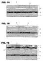
- FIGS. 1A to 1Hare partial sectional views illustrating a part of a method for fabricating a field-effect transistor according to an embodiment of the present invention.
- FIG. 2is a graph for explaining an action of the present invention and a SIMS result illustrating boron concentration distribution in a channel region.
- FIGS. 1A to 1Hshow an essential part of a method for fabricating a semiconductor device of the present invention.
- a buried oxide film 2 and a SOI layer 3are formed on a silicon substrate 1 , and a SOI substrate is formed as shown in FIG. 1A .
- the film thickness of the SOI layer 3is preferably such that a fully depleted type transistor can be formed and impurity distribution can be formed by ion-implantation in the channel region, which is 20 to 50 nm. If the thickness of the SOI layer 3 is smaller than 20 nm, for example, the impurity amount to be introduced into the SOI layer is fluctuated by diffusion at ion-implantation, and formation of a practical transistor becomes difficult.
- an impurity 5is ion-implanted in the channel region for threshold voltage control in the SOI substrate.
- the impurity 5P-type impurity such as boron, BF 2 or indium is used for an N-type MOSFET.
- a P-type impuritysuch as arsenic or phosphorus is used.
- implanting energyis selected so that its concentration peak exists in the SOI layer, which is ion implantation of approximately 1 ⁇ 10 12 to 1 ⁇ 10 13 cm ⁇ 2 .
- the concentration peak of the impurity 5is distributed in the vicinity of the center in the SOI layer 3 as much as possible, when seen in the thickness direction of the SOI layer 3 .
- the fluctuation of the implanted impurity 5can be reduced.
- channel-annealingis carried out at an implantation acceleration 18 keV (BF 2 ) in a nitrogen atmosphere, for example.
- the channel-annealingis continuously carried out for 5 to 90 minutes in a range 600 to 750° C.
- the annealing treatmentas shown in FIG. 1B , excessive enhanced diffusion is caused in the implanted impurity 5 , which is moved to the vicinity of a boundary (surface of the SOI layer) between a gate insulating film ( 6 ) and the SOI layer 3 .
- the impurity 5is distributed with a high concentration in the vicinity of the boundary with the gate insulating film ( 6 ) rather than the vicinity of the boundary with the buried insulating film 2 .
- the channel-annealing temperatureexceeds 750° C.
- the impurity amount moving to the vicinity of the Si surfaceis decreased.
- the annealing timefalls below 5 minutes, extra interstitial silicon introduced into the Si substrate by ion implantation remains in the substrate and causes re-diffusion of the impurity having been moved to the vicinity of the surface in the substrate by the subsequent heat treatment. It is possible to set the anneal temperature at 600° C. or less, but it makes a required annealing time remarkably longer than 90 minutes, which lowers the throughput.
- channel-annealinga nitrogen atmosphere or the like is used so that the channel region is not exposed to an oxidized atmosphere.
- the relation between the channel-annealing temperature and timeshall be as follows with the channel-annealing temperature at T (K) and channel-annealing time as t (minutes): 506 ⁇ 1000 /T ⁇ 490 ⁇ t ⁇ 400 ⁇ 1000 /T ⁇ 386
- This formulais derived from results of a theoretical experiment of calibration based on actual measurement.
- the working effect of the present inventioncan be obtained on the low temperature side even if time is somewhat longer. However, in the above range, a process with a shorter treatment time and higher throughput can be obtained. With this condition, a semiconductor device can be stably manufactured, even allowing for errors between equipment.
- a gate insulating film 6is formed on the SOI layer 3 .
- the formation of the gate insulating film 6may be either before or after introduction of the impurity 5 into the channel region 4 . Since the annealing treatment after formation of the gate insulating film is carried out through a thin gate insulating film, oxidation progresses in an oxidized atmosphere, and thus, annealing treatment in a non-oxidized atmosphere is important.
- a polysilicon layer 7is formed for a gate electrode.
- a gate impurityphosphorus or arsenic, for example, may be implanted for the N-type MOSFET, while boron or BF2, for example, may be implanted for the P-type MOSFET.
- the ion-implantation dose amount of this gate impurityis set approximately at 2 ⁇ 10 15 cm ⁇ 2 , for example.
- the polysilicon layer 7 and the gate insulating film 6are given patterning so as to form a gate electrode 8 .
- An extremely thin oxide filmmay be formed in advance on the surface of the gate electrode 8 by oxidation treatment.
- a pocket 9is formed by ion implantation of ion of the same conductive type as an ion species in the channel region into the surface layer portion of the SOI layer 3 .
- This pocket 9restricts threshold voltage drop at on/off of a transistor.
- an LDD (Lightly Doped Drain) region 10 with the impurity concentration lower than the impurity concentration in the normal source/drain region by a single- or double-digit figureis provided ( FIG. 1F ).
- the LDD region 10is formed by implanting phosphorus or arsenic for the N-type MOSFET or boron or BF 2 for the P-type MOSFET, for example.
- a side wall 11is formed on the side faces of the gate electrode 8 and the gate insulating film 6 .
- the side wall 11is formed by accumulating a silicon nitride film and etching it back, for example.
- a diffusion layer 12is formed by ion implantation of the impurity.
- phosphorus or arsenicis implanted for the N-type MOSFET, while boron or BF 2 may be ion-implanted for the P-type MOSFET.
- the impurity introduced into the channel region 4has a dose amount of 1 ⁇ 10 12 to 1 ⁇ 10 13 cm ⁇ 2 .
- excess interstitial siliconis generated in an amount of approximately 5 ⁇ 10 12 to 3 ⁇ 10 13 cm ⁇ 2 .
- the silicon regionis not made into amorphous but all the generated interstitial silicon contributes to diffusion.
- the impurity bonded to the excess interstitial silicon (dopant)is diffused at a speed extremely higher than that of impurity diffusion in a normal thermal equilibrium. This is called transient enhanced diffusion. The degree of dopant diffusion in the transient enhanced diffusion depends on the dopant amount to be bonded to the interstitial silicon.
- the interstitial siliconis bonded to a silicon atom on the interface between oxide silicon and silicon single crystal during the course of annealing and disappears.
- the interstitial siliconremains sufficiently longer than the bonding speed between the interstitial silicon and the dopant.
- the transient enhanced diffusionis a phenomenon found in the diffusion layer 12 and the LDD layer 10 , but not in the channel region 4 .
- the large amount of generated interstitial siliconcauses the transient enhanced diffusion.
- the LDD layer 10since the shallow peak impurity concentration and close to the interface with the gate insulating film causes the similar diffusion. In channel formation by a bulk silicon device, the peak position of the impurity concentration is as deep as approximately 80 nm in the shallow case. Also, since the concentration of the introduced impurity is low, the amount of generated interstitial silicon is small. Therefore, the transient enhanced diffusion does not occur with the bulk silicon device.
- the film thickness of the SOI layer 3 of the present inventionis approximately 20 to 50 nm, and the concentration peak of the impurity at ion implantation is made to exist in the SOI layer 3 .
- the concentration peak by this ion implantationis 50 nm at the deepest.
- FIG. 2An SIMS result examining boron concentration distribution in the channel region before and after the channel-annealing by ion implantation of BF 2 of 5E 12 cm ⁇ 2 in the SOI layer with the film thickness of 40 nm is shown in FIG. 2 .
- the unit of boron concentration(vertical axis) is cm 3 .
- the profile immediately after ion implantation of BF 2is indicated by a dot line.
- the profile after the channel-annealing at 620° C. for 70 minutesis indicated by a solid line.
- the concentration peak of the impurityexists in the vicinity of the center in the SOI layer.
- the impurity concentration close to the surfacebecomes higher.
- the dopant profile (impurity distribution) in which the concentration is steeply lowered toward the deep portion in the SOI layeris obtained by the channel-annealing.
- interstitial siliconmay be introduced by silicon implantation. By this arrangement, fluctuation in excess interstitial silicon distribution can be reduced.
Landscapes
- Thin Film Transistor (AREA)
Abstract
Description
506×1000/T−490<t<400×1000/T−386
- 1: Silicon substrate
- 3: SOI layer
- 5: Impurity (dopant)
- 8: Gate electrode
- 9: Pocket
- 10: LDD region
- 12: Diffusion layer
506×1000/T−490<t<400×1000/T−386
Claims (8)
Applications Claiming Priority (2)
| Application Number | Priority Date | Filing Date | Title |
|---|---|---|---|
| JP2006266316AJP2008085253A (en) | 2006-09-29 | 2006-09-29 | Manufacturing method of semiconductor device |
| JP2006-266316 | 2006-09-29 |
Publications (2)
| Publication Number | Publication Date |
|---|---|
| US20080081402A1 US20080081402A1 (en) | 2008-04-03 |
| US7811873B2true US7811873B2 (en) | 2010-10-12 |
Family
ID=39261601
Family Applications (1)
| Application Number | Title | Priority Date | Filing Date |
|---|---|---|---|
| US11/853,070Expired - Fee RelatedUS7811873B2 (en) | 2006-09-29 | 2007-09-11 | Method for fabricating MOS-FET |
Country Status (2)
| Country | Link |
|---|---|
| US (1) | US7811873B2 (en) |
| JP (1) | JP2008085253A (en) |
Cited By (46)
| Publication number | Priority date | Publication date | Assignee | Title |
|---|---|---|---|---|
| US8404551B2 (en) | 2010-12-03 | 2013-03-26 | Suvolta, Inc. | Source/drain extension control for advanced transistors |
| US8421162B2 (en) | 2009-09-30 | 2013-04-16 | Suvolta, Inc. | Advanced transistors with punch through suppression |
| US8461875B1 (en) | 2011-02-18 | 2013-06-11 | Suvolta, Inc. | Digital circuits having improved transistors, and methods therefor |
| US8525271B2 (en) | 2011-03-03 | 2013-09-03 | Suvolta, Inc. | Semiconductor structure with improved channel stack and method for fabrication thereof |
| US8530286B2 (en) | 2010-04-12 | 2013-09-10 | Suvolta, Inc. | Low power semiconductor transistor structure and method of fabrication thereof |
| US8569128B2 (en) | 2010-06-21 | 2013-10-29 | Suvolta, Inc. | Semiconductor structure and method of fabrication thereof with mixed metal types |
| US8569156B1 (en) | 2011-05-16 | 2013-10-29 | Suvolta, Inc. | Reducing or eliminating pre-amorphization in transistor manufacture |
| US8599623B1 (en) | 2011-12-23 | 2013-12-03 | Suvolta, Inc. | Circuits and methods for measuring circuit elements in an integrated circuit device |
| US8614128B1 (en) | 2011-08-23 | 2013-12-24 | Suvolta, Inc. | CMOS structures and processes based on selective thinning |
| US8629016B1 (en) | 2011-07-26 | 2014-01-14 | Suvolta, Inc. | Multiple transistor types formed in a common epitaxial layer by differential out-diffusion from a doped underlayer |
| US8637955B1 (en) | 2012-08-31 | 2014-01-28 | Suvolta, Inc. | Semiconductor structure with reduced junction leakage and method of fabrication thereof |
| US8645878B1 (en) | 2011-08-23 | 2014-02-04 | Suvolta, Inc. | Porting a circuit design from a first semiconductor process to a second semiconductor process |
| US8713511B1 (en) | 2011-09-16 | 2014-04-29 | Suvolta, Inc. | Tools and methods for yield-aware semiconductor manufacturing process target generation |
| US8735987B1 (en) | 2011-06-06 | 2014-05-27 | Suvolta, Inc. | CMOS gate stack structures and processes |
| US8748270B1 (en) | 2011-03-30 | 2014-06-10 | Suvolta, Inc. | Process for manufacturing an improved analog transistor |
| US8748986B1 (en) | 2011-08-05 | 2014-06-10 | Suvolta, Inc. | Electronic device with controlled threshold voltage |
| US8759872B2 (en) | 2010-06-22 | 2014-06-24 | Suvolta, Inc. | Transistor with threshold voltage set notch and method of fabrication thereof |
| US8796048B1 (en) | 2011-05-11 | 2014-08-05 | Suvolta, Inc. | Monitoring and measurement of thin film layers |
| US8811068B1 (en) | 2011-05-13 | 2014-08-19 | Suvolta, Inc. | Integrated circuit devices and methods |
| US8816754B1 (en) | 2012-11-02 | 2014-08-26 | Suvolta, Inc. | Body bias circuits and methods |
| US8819603B1 (en) | 2011-12-15 | 2014-08-26 | Suvolta, Inc. | Memory circuits and methods of making and designing the same |
| US8863064B1 (en) | 2012-03-23 | 2014-10-14 | Suvolta, Inc. | SRAM cell layout structure and devices therefrom |
| US8877619B1 (en) | 2012-01-23 | 2014-11-04 | Suvolta, Inc. | Process for manufacture of integrated circuits with different channel doping transistor architectures and devices therefrom |
| US8883600B1 (en) | 2011-12-22 | 2014-11-11 | Suvolta, Inc. | Transistor having reduced junction leakage and methods of forming thereof |
| US8895327B1 (en) | 2011-12-09 | 2014-11-25 | Suvolta, Inc. | Tipless transistors, short-tip transistors, and methods and circuits therefor |
| US8970289B1 (en) | 2012-01-23 | 2015-03-03 | Suvolta, Inc. | Circuits and devices for generating bi-directional body bias voltages, and methods therefor |
| US8995204B2 (en) | 2011-06-23 | 2015-03-31 | Suvolta, Inc. | Circuit devices and methods having adjustable transistor body bias |
| US8999861B1 (en) | 2011-05-11 | 2015-04-07 | Suvolta, Inc. | Semiconductor structure with substitutional boron and method for fabrication thereof |
| US9041126B2 (en) | 2012-09-21 | 2015-05-26 | Mie Fujitsu Semiconductor Limited | Deeply depleted MOS transistors having a screening layer and methods thereof |
| US9054219B1 (en) | 2011-08-05 | 2015-06-09 | Mie Fujitsu Semiconductor Limited | Semiconductor devices having fin structures and fabrication methods thereof |
| US9070477B1 (en) | 2012-12-12 | 2015-06-30 | Mie Fujitsu Semiconductor Limited | Bit interleaved low voltage static random access memory (SRAM) and related methods |
| US9093550B1 (en) | 2012-01-31 | 2015-07-28 | Mie Fujitsu Semiconductor Limited | Integrated circuits having a plurality of high-K metal gate FETs with various combinations of channel foundation structure and gate stack structure and methods of making same |
| US9093997B1 (en) | 2012-11-15 | 2015-07-28 | Mie Fujitsu Semiconductor Limited | Slew based process and bias monitors and related methods |
| US9112484B1 (en) | 2012-12-20 | 2015-08-18 | Mie Fujitsu Semiconductor Limited | Integrated circuit process and bias monitors and related methods |
| US9112057B1 (en) | 2012-09-18 | 2015-08-18 | Mie Fujitsu Semiconductor Limited | Semiconductor devices with dopant migration suppression and method of fabrication thereof |
| US9236466B1 (en) | 2011-10-07 | 2016-01-12 | Mie Fujitsu Semiconductor Limited | Analog circuits having improved insulated gate transistors, and methods therefor |
| US9263346B2 (en) | 2013-01-18 | 2016-02-16 | Renesas Electronics Corporation | Semiconductor device with silicon layer containing carbon |
| US9268885B1 (en) | 2013-02-28 | 2016-02-23 | Mie Fujitsu Semiconductor Limited | Integrated circuit device methods and models with predicted device metric variations |
| US9299698B2 (en) | 2012-06-27 | 2016-03-29 | Mie Fujitsu Semiconductor Limited | Semiconductor structure with multiple transistors having various threshold voltages |
| US9299801B1 (en) | 2013-03-14 | 2016-03-29 | Mie Fujitsu Semiconductor Limited | Method for fabricating a transistor device with a tuned dopant profile |
| US9319013B2 (en) | 2014-08-19 | 2016-04-19 | Mie Fujitsu Semiconductor Limited | Operational amplifier input offset correction with transistor threshold voltage adjustment |
| US9406567B1 (en) | 2012-02-28 | 2016-08-02 | Mie Fujitsu Semiconductor Limited | Method for fabricating multiple transistor devices on a substrate with varying threshold voltages |
| US9431068B2 (en) | 2012-10-31 | 2016-08-30 | Mie Fujitsu Semiconductor Limited | Dynamic random access memory (DRAM) with low variation transistor peripheral circuits |
| US9478571B1 (en) | 2013-05-24 | 2016-10-25 | Mie Fujitsu Semiconductor Limited | Buried channel deeply depleted channel transistor |
| US9710006B2 (en) | 2014-07-25 | 2017-07-18 | Mie Fujitsu Semiconductor Limited | Power up body bias circuits and methods |
| US10074568B2 (en) | 2009-09-30 | 2018-09-11 | Mie Fujitsu Semiconductor Limited | Electronic devices and systems, and methods for making and using same |
Families Citing this family (2)
| Publication number | Priority date | Publication date | Assignee | Title |
|---|---|---|---|---|
| JP2011176039A (en)* | 2010-02-23 | 2011-09-08 | Oki Semiconductor Co Ltd | Semiconductor integrated device, and method of manufacturing the same |
| JP2012004471A (en)* | 2010-06-21 | 2012-01-05 | Toshiba Corp | Semiconductor device and method of manufacturing the same |
Citations (5)
| Publication number | Priority date | Publication date | Assignee | Title |
|---|---|---|---|---|
| JP2000349295A (en) | 1999-06-08 | 2000-12-15 | Nec Corp | Field effect transistor and its manufacture |
| JP2002270846A (en) | 2001-03-12 | 2002-09-20 | Oki Electric Ind Co Ltd | Method for manufacturing semiconductor device |
| US20030122164A1 (en)* | 2001-02-07 | 2003-07-03 | Hiroshi Komatsu | Semiconductor device and its manufacturing method |
| US6861322B2 (en)* | 2001-05-29 | 2005-03-01 | Oki Electric Industry Co., Ltd. | Method of manufacturing a semiconductor device |
| US20090023269A1 (en)* | 2003-09-05 | 2009-01-22 | Nobuyuki Morimoto | Method for producing soi wafer |
- 2006
- 2006-09-29JPJP2006266316Apatent/JP2008085253A/enactivePending
- 2007
- 2007-09-11USUS11/853,070patent/US7811873B2/ennot_activeExpired - Fee Related
Patent Citations (6)
| Publication number | Priority date | Publication date | Assignee | Title |
|---|---|---|---|---|
| JP2000349295A (en) | 1999-06-08 | 2000-12-15 | Nec Corp | Field effect transistor and its manufacture |
| US20030122164A1 (en)* | 2001-02-07 | 2003-07-03 | Hiroshi Komatsu | Semiconductor device and its manufacturing method |
| JP2002270846A (en) | 2001-03-12 | 2002-09-20 | Oki Electric Ind Co Ltd | Method for manufacturing semiconductor device |
| US6825074B2 (en) | 2001-03-12 | 2004-11-30 | Oki Electric Industry Co., Ltd. | Method of manufacturing a silicon-on-insulator (SOI) semiconductor device |
| US6861322B2 (en)* | 2001-05-29 | 2005-03-01 | Oki Electric Industry Co., Ltd. | Method of manufacturing a semiconductor device |
| US20090023269A1 (en)* | 2003-09-05 | 2009-01-22 | Nobuyuki Morimoto | Method for producing soi wafer |
Cited By (97)
| Publication number | Priority date | Publication date | Assignee | Title |
|---|---|---|---|---|
| US8421162B2 (en) | 2009-09-30 | 2013-04-16 | Suvolta, Inc. | Advanced transistors with punch through suppression |
| US10074568B2 (en) | 2009-09-30 | 2018-09-11 | Mie Fujitsu Semiconductor Limited | Electronic devices and systems, and methods for making and using same |
| US10217668B2 (en) | 2009-09-30 | 2019-02-26 | Mie Fujitsu Semiconductor Limited | Electronic devices and systems, and methods for making and using the same |
| US10224244B2 (en) | 2009-09-30 | 2019-03-05 | Mie Fujitsu Semiconductor Limited | Electronic devices and systems, and methods for making and using the same |
| US10325986B2 (en) | 2009-09-30 | 2019-06-18 | Mie Fujitsu Semiconductor Limited | Advanced transistors with punch through suppression |
| US9263523B2 (en) | 2009-09-30 | 2016-02-16 | Mie Fujitsu Semiconductor Limited | Advanced transistors with punch through suppression |
| US11887895B2 (en) | 2009-09-30 | 2024-01-30 | United Semiconductor Japan Co., Ltd. | Electronic devices and systems, and methods for making and using the same |
| US9508800B2 (en) | 2009-09-30 | 2016-11-29 | Mie Fujitsu Semiconductor Limited | Advanced transistors with punch through suppression |
| US11062950B2 (en) | 2009-09-30 | 2021-07-13 | United Semiconductor Japan Co., Ltd. | Electronic devices and systems, and methods for making and using the same |
| US9496261B2 (en) | 2010-04-12 | 2016-11-15 | Mie Fujitsu Semiconductor Limited | Low power semiconductor transistor structure and method of fabrication thereof |
| US8530286B2 (en) | 2010-04-12 | 2013-09-10 | Suvolta, Inc. | Low power semiconductor transistor structure and method of fabrication thereof |
| US9865596B2 (en) | 2010-04-12 | 2018-01-09 | Mie Fujitsu Semiconductor Limited | Low power semiconductor transistor structure and method of fabrication thereof |
| US9224733B2 (en) | 2010-06-21 | 2015-12-29 | Mie Fujitsu Semiconductor Limited | Semiconductor structure and method of fabrication thereof with mixed metal types |
| US8569128B2 (en) | 2010-06-21 | 2013-10-29 | Suvolta, Inc. | Semiconductor structure and method of fabrication thereof with mixed metal types |
| US8759872B2 (en) | 2010-06-22 | 2014-06-24 | Suvolta, Inc. | Transistor with threshold voltage set notch and method of fabrication thereof |
| US9922977B2 (en) | 2010-06-22 | 2018-03-20 | Mie Fujitsu Semiconductor Limited | Transistor with threshold voltage set notch and method of fabrication thereof |
| US9418987B2 (en) | 2010-06-22 | 2016-08-16 | Mie Fujitsu Semiconductor Limited | Transistor with threshold voltage set notch and method of fabrication thereof |
| US8404551B2 (en) | 2010-12-03 | 2013-03-26 | Suvolta, Inc. | Source/drain extension control for advanced transistors |
| US9006843B2 (en) | 2010-12-03 | 2015-04-14 | Suvolta, Inc. | Source/drain extension control for advanced transistors |
| US8686511B2 (en) | 2010-12-03 | 2014-04-01 | Suvolta, Inc. | Source/drain extension control for advanced transistors |
| US8563384B2 (en) | 2010-12-03 | 2013-10-22 | Suvolta, Inc. | Source/drain extension control for advanced transistors |
| US9838012B2 (en) | 2011-02-18 | 2017-12-05 | Mie Fujitsu Semiconductor Limited | Digital circuits having improved transistors, and methods therefor |
| US8461875B1 (en) | 2011-02-18 | 2013-06-11 | Suvolta, Inc. | Digital circuits having improved transistors, and methods therefor |
| US9680470B2 (en) | 2011-02-18 | 2017-06-13 | Mie Fujitsu Semiconductor Limited | Digital circuits having improved transistors, and methods therefor |
| US9985631B2 (en) | 2011-02-18 | 2018-05-29 | Mie Fujitsu Semiconductor Limited | Digital circuits having improved transistors, and methods therefor |
| US9184750B1 (en) | 2011-02-18 | 2015-11-10 | Mie Fujitsu Semiconductor Limited | Digital circuits having improved transistors, and methods therefor |
| US10250257B2 (en) | 2011-02-18 | 2019-04-02 | Mie Fujitsu Semiconductor Limited | Digital circuits having improved transistors, and methods therefor |
| US8525271B2 (en) | 2011-03-03 | 2013-09-03 | Suvolta, Inc. | Semiconductor structure with improved channel stack and method for fabrication thereof |
| US9111785B2 (en) | 2011-03-03 | 2015-08-18 | Mie Fujitsu Semiconductor Limited | Semiconductor structure with improved channel stack and method for fabrication thereof |
| US9093469B2 (en) | 2011-03-30 | 2015-07-28 | Mie Fujitsu Semiconductor Limited | Analog transistor |
| US8748270B1 (en) | 2011-03-30 | 2014-06-10 | Suvolta, Inc. | Process for manufacturing an improved analog transistor |
| US8999861B1 (en) | 2011-05-11 | 2015-04-07 | Suvolta, Inc. | Semiconductor structure with substitutional boron and method for fabrication thereof |
| US8796048B1 (en) | 2011-05-11 | 2014-08-05 | Suvolta, Inc. | Monitoring and measurement of thin film layers |
| US8811068B1 (en) | 2011-05-13 | 2014-08-19 | Suvolta, Inc. | Integrated circuit devices and methods |
| US9741428B2 (en) | 2011-05-13 | 2017-08-22 | Mie Fujitsu Semiconductor Limited | Integrated circuit devices and methods |
| US9966130B2 (en) | 2011-05-13 | 2018-05-08 | Mie Fujitsu Semiconductor Limited | Integrated circuit devices and methods |
| US9362291B1 (en) | 2011-05-13 | 2016-06-07 | Mie Fujitsu Semiconductor Limited | Integrated circuit devices and methods |
| US8937005B2 (en) | 2011-05-16 | 2015-01-20 | Suvolta, Inc. | Reducing or eliminating pre-amorphization in transistor manufacture |
| US9514940B2 (en) | 2011-05-16 | 2016-12-06 | Mie Fujitsu Semiconductor Limited | Reducing or eliminating pre-amorphization in transistor manufacture |
| US8569156B1 (en) | 2011-05-16 | 2013-10-29 | Suvolta, Inc. | Reducing or eliminating pre-amorphization in transistor manufacture |
| US9793172B2 (en) | 2011-05-16 | 2017-10-17 | Mie Fujitsu Semiconductor Limited | Reducing or eliminating pre-amorphization in transistor manufacture |
| US8735987B1 (en) | 2011-06-06 | 2014-05-27 | Suvolta, Inc. | CMOS gate stack structures and processes |
| US9281248B1 (en) | 2011-06-06 | 2016-03-08 | Mie Fujitsu Semiconductor Limited | CMOS gate stack structures and processes |
| US8995204B2 (en) | 2011-06-23 | 2015-03-31 | Suvolta, Inc. | Circuit devices and methods having adjustable transistor body bias |
| US8653604B1 (en) | 2011-07-26 | 2014-02-18 | Suvolta, Inc. | Multiple transistor types formed in a common epitaxial layer by differential out-diffusion from a doped underlayer |
| US8916937B1 (en) | 2011-07-26 | 2014-12-23 | Suvolta, Inc. | Multiple transistor types formed in a common epitaxial layer by differential out-diffusion from a doped underlayer |
| US8629016B1 (en) | 2011-07-26 | 2014-01-14 | Suvolta, Inc. | Multiple transistor types formed in a common epitaxial layer by differential out-diffusion from a doped underlayer |
| US8963249B1 (en) | 2011-08-05 | 2015-02-24 | Suvolta, Inc. | Electronic device with controlled threshold voltage |
| US8748986B1 (en) | 2011-08-05 | 2014-06-10 | Suvolta, Inc. | Electronic device with controlled threshold voltage |
| US9054219B1 (en) | 2011-08-05 | 2015-06-09 | Mie Fujitsu Semiconductor Limited | Semiconductor devices having fin structures and fabrication methods thereof |
| US8645878B1 (en) | 2011-08-23 | 2014-02-04 | Suvolta, Inc. | Porting a circuit design from a first semiconductor process to a second semiconductor process |
| US9117746B1 (en) | 2011-08-23 | 2015-08-25 | Mie Fujitsu Semiconductor Limited | Porting a circuit design from a first semiconductor process to a second semiconductor process |
| US9391076B1 (en) | 2011-08-23 | 2016-07-12 | Mie Fujitsu Semiconductor Limited | CMOS structures and processes based on selective thinning |
| US8614128B1 (en) | 2011-08-23 | 2013-12-24 | Suvolta, Inc. | CMOS structures and processes based on selective thinning |
| US8806395B1 (en) | 2011-08-23 | 2014-08-12 | Suvolta, Inc. | Porting a circuit design from a first semiconductor process to a second semiconductor process |
| US8713511B1 (en) | 2011-09-16 | 2014-04-29 | Suvolta, Inc. | Tools and methods for yield-aware semiconductor manufacturing process target generation |
| US9236466B1 (en) | 2011-10-07 | 2016-01-12 | Mie Fujitsu Semiconductor Limited | Analog circuits having improved insulated gate transistors, and methods therefor |
| US8895327B1 (en) | 2011-12-09 | 2014-11-25 | Suvolta, Inc. | Tipless transistors, short-tip transistors, and methods and circuits therefor |
| US8819603B1 (en) | 2011-12-15 | 2014-08-26 | Suvolta, Inc. | Memory circuits and methods of making and designing the same |
| US9196727B2 (en) | 2011-12-22 | 2015-11-24 | Mie Fujitsu Semiconductor Limited | High uniformity screen and epitaxial layers for CMOS devices |
| US9368624B2 (en) | 2011-12-22 | 2016-06-14 | Mie Fujitsu Semiconductor Limited | Method for fabricating a transistor with reduced junction leakage current |
| US8883600B1 (en) | 2011-12-22 | 2014-11-11 | Suvolta, Inc. | Transistor having reduced junction leakage and methods of forming thereof |
| US8599623B1 (en) | 2011-12-23 | 2013-12-03 | Suvolta, Inc. | Circuits and methods for measuring circuit elements in an integrated circuit device |
| US8877619B1 (en) | 2012-01-23 | 2014-11-04 | Suvolta, Inc. | Process for manufacture of integrated circuits with different channel doping transistor architectures and devices therefrom |
| US8970289B1 (en) | 2012-01-23 | 2015-03-03 | Suvolta, Inc. | Circuits and devices for generating bi-directional body bias voltages, and methods therefor |
| US9385047B2 (en) | 2012-01-31 | 2016-07-05 | Mie Fujitsu Semiconductor Limited | Integrated circuits having a plurality of high-K metal gate FETs with various combinations of channel foundation structure and gate stack structure and methods of making same |
| US9093550B1 (en) | 2012-01-31 | 2015-07-28 | Mie Fujitsu Semiconductor Limited | Integrated circuits having a plurality of high-K metal gate FETs with various combinations of channel foundation structure and gate stack structure and methods of making same |
| US9406567B1 (en) | 2012-02-28 | 2016-08-02 | Mie Fujitsu Semiconductor Limited | Method for fabricating multiple transistor devices on a substrate with varying threshold voltages |
| US8863064B1 (en) | 2012-03-23 | 2014-10-14 | Suvolta, Inc. | SRAM cell layout structure and devices therefrom |
| US10014387B2 (en) | 2012-06-27 | 2018-07-03 | Mie Fujitsu Semiconductor Limited | Semiconductor structure with multiple transistors having various threshold voltages |
| US10217838B2 (en) | 2012-06-27 | 2019-02-26 | Mie Fujitsu Semiconductor Limited | Semiconductor structure with multiple transistors having various threshold voltages |
| US9812550B2 (en) | 2012-06-27 | 2017-11-07 | Mie Fujitsu Semiconductor Limited | Semiconductor structure with multiple transistors having various threshold voltages |
| US9299698B2 (en) | 2012-06-27 | 2016-03-29 | Mie Fujitsu Semiconductor Limited | Semiconductor structure with multiple transistors having various threshold voltages |
| US8637955B1 (en) | 2012-08-31 | 2014-01-28 | Suvolta, Inc. | Semiconductor structure with reduced junction leakage and method of fabrication thereof |
| US9105711B2 (en) | 2012-08-31 | 2015-08-11 | Mie Fujitsu Semiconductor Limited | Semiconductor structure with reduced junction leakage and method of fabrication thereof |
| US9112057B1 (en) | 2012-09-18 | 2015-08-18 | Mie Fujitsu Semiconductor Limited | Semiconductor devices with dopant migration suppression and method of fabrication thereof |
| US9041126B2 (en) | 2012-09-21 | 2015-05-26 | Mie Fujitsu Semiconductor Limited | Deeply depleted MOS transistors having a screening layer and methods thereof |
| US9431068B2 (en) | 2012-10-31 | 2016-08-30 | Mie Fujitsu Semiconductor Limited | Dynamic random access memory (DRAM) with low variation transistor peripheral circuits |
| US8816754B1 (en) | 2012-11-02 | 2014-08-26 | Suvolta, Inc. | Body bias circuits and methods |
| US9154123B1 (en) | 2012-11-02 | 2015-10-06 | Mie Fujitsu Semiconductor Limited | Body bias circuits and methods |
| US9319034B2 (en) | 2012-11-15 | 2016-04-19 | Mie Fujitsu Semiconductor Limited | Slew based process and bias monitors and related methods |
| US9093997B1 (en) | 2012-11-15 | 2015-07-28 | Mie Fujitsu Semiconductor Limited | Slew based process and bias monitors and related methods |
| US9070477B1 (en) | 2012-12-12 | 2015-06-30 | Mie Fujitsu Semiconductor Limited | Bit interleaved low voltage static random access memory (SRAM) and related methods |
| US9276561B2 (en) | 2012-12-20 | 2016-03-01 | Mie Fujitsu Semiconductor Limited | Integrated circuit process and bias monitors and related methods |
| US9112484B1 (en) | 2012-12-20 | 2015-08-18 | Mie Fujitsu Semiconductor Limited | Integrated circuit process and bias monitors and related methods |
| US9722044B2 (en) | 2013-01-18 | 2017-08-01 | Renesas Electronics Corporation | Manufacturing method of semiconductor device with silicon layer containing carbon |
| US10411112B2 (en) | 2013-01-18 | 2019-09-10 | Renesas Electronics Corporation | Semiconductor device with silicon layer containing carbon |
| US9263346B2 (en) | 2013-01-18 | 2016-02-16 | Renesas Electronics Corporation | Semiconductor device with silicon layer containing carbon |
| US9268885B1 (en) | 2013-02-28 | 2016-02-23 | Mie Fujitsu Semiconductor Limited | Integrated circuit device methods and models with predicted device metric variations |
| US9299801B1 (en) | 2013-03-14 | 2016-03-29 | Mie Fujitsu Semiconductor Limited | Method for fabricating a transistor device with a tuned dopant profile |
| US9893148B2 (en) | 2013-03-14 | 2018-02-13 | Mie Fujitsu Semiconductor Limited | Method for fabricating a transistor device with a tuned dopant profile |
| US9577041B2 (en) | 2013-03-14 | 2017-02-21 | Mie Fujitsu Semiconductor Limited | Method for fabricating a transistor device with a tuned dopant profile |
| US9786703B2 (en) | 2013-05-24 | 2017-10-10 | Mie Fujitsu Semiconductor Limited | Buried channel deeply depleted channel transistor |
| US9478571B1 (en) | 2013-05-24 | 2016-10-25 | Mie Fujitsu Semiconductor Limited | Buried channel deeply depleted channel transistor |
| US9991300B2 (en) | 2013-05-24 | 2018-06-05 | Mie Fujitsu Semiconductor Limited | Buried channel deeply depleted channel transistor |
| US9710006B2 (en) | 2014-07-25 | 2017-07-18 | Mie Fujitsu Semiconductor Limited | Power up body bias circuits and methods |
| US9319013B2 (en) | 2014-08-19 | 2016-04-19 | Mie Fujitsu Semiconductor Limited | Operational amplifier input offset correction with transistor threshold voltage adjustment |
Also Published As
| Publication number | Publication date |
|---|---|
| US20080081402A1 (en) | 2008-04-03 |
| JP2008085253A (en) | 2008-04-10 |
Similar Documents
| Publication | Publication Date | Title |
|---|---|---|
| US7811873B2 (en) | Method for fabricating MOS-FET | |
| US6372591B1 (en) | Fabrication method of semiconductor device using ion implantation | |
| US7195987B2 (en) | Methods of forming CMOS integrated circuit devices and substrates having buried silicon germanium layers therein | |
| US7091093B1 (en) | Method for fabricating a semiconductor device having a pocket dopant diffused layer | |
| US8067805B2 (en) | Ultra shallow junction formation by epitaxial interface limited diffusion | |
| US6881987B2 (en) | pMOS device having ultra shallow super-steep-retrograde epi-channel with dual channel doping and method for fabricating the same | |
| US7118980B2 (en) | Solid phase epitaxy recrystallization by laser annealing | |
| US7700450B2 (en) | Method for forming MOS transistor | |
| EP0789400A2 (en) | Semiconductor device and method for fabricating the same | |
| US5909622A (en) | Asymmetrical p-channel transistor formed by nitrided oxide and large tilt angle LDD implant | |
| JP2007073578A (en) | Semiconductor device and manufacturing method thereof | |
| US8440514B2 (en) | Semiconductor device and method for manufacturing the same | |
| US5893739A (en) | Asymmetrical P-channel transistor having a boron migration barrier and a selectively formed sidewall spacer | |
| US20060284249A1 (en) | Impurity co-implantation to improve transistor performance | |
| US6432802B1 (en) | Method for fabricating semiconductor device | |
| JPH1050988A (en) | Insulated gate field effect transistor and method of manufacturing the same | |
| US20060275964A1 (en) | Semiconductor device and method for fabricating the same | |
| US6104064A (en) | Asymmetrical transistor structure | |
| US6080630A (en) | Method for forming a MOS device with self-compensating VT -implants | |
| JPH10256539A (en) | Semiconductor device and manufacturing method thereof | |
| US5783458A (en) | Asymmetrical p-channel transistor having nitrided oxide patterned to allow select formation of a grown sidewall spacer | |
| US6847089B2 (en) | Gate edge diode leakage reduction | |
| US7151032B2 (en) | Methods of fabricating semiconductor devices | |
| JPH10341017A (en) | Fabrication of mis transistor | |
| US7019363B1 (en) | MOS transistor with asymmetrical source/drain extensions |
Legal Events
| Date | Code | Title | Description |
|---|---|---|---|
| AS | Assignment | Owner name:OKI ELECTRIC INDUSTRY CO., LTD., JAPAN Free format text:ASSIGNMENT OF ASSIGNORS INTEREST;ASSIGNOR:MOCHIZUKI, MARIE;REEL/FRAME:019813/0295 Effective date:20070827 | |
| AS | Assignment | Owner name:OKI SEMICONDUCTOR CO., LTD., JAPAN Free format text:CHANGE OF NAME;ASSIGNOR:OKI ELECTRIC INDUSTRY CO., LTD.;REEL/FRAME:022162/0586 Effective date:20081001 Owner name:OKI SEMICONDUCTOR CO., LTD.,JAPAN Free format text:CHANGE OF NAME;ASSIGNOR:OKI ELECTRIC INDUSTRY CO., LTD.;REEL/FRAME:022162/0586 Effective date:20081001 | |
| AS | Assignment | Owner name:LAPIS SEMICONDUCTOR CO., LTD., JAPAN Free format text:CHANGE OF NAME;ASSIGNOR:OKI SEMICONDUCTOR CO., LTD;REEL/FRAME:032495/0483 Effective date:20111003 | |
| REMI | Maintenance fee reminder mailed | ||
| LAPS | Lapse for failure to pay maintenance fees | ||
| STCH | Information on status: patent discontinuation | Free format text:PATENT EXPIRED DUE TO NONPAYMENT OF MAINTENANCE FEES UNDER 37 CFR 1.362 | |
| FP | Lapsed due to failure to pay maintenance fee | Effective date:20141012 |