US7811421B2 - High deposition rate sputtering - Google Patents
High deposition rate sputteringDownload PDFInfo
- Publication number
- US7811421B2 US7811421B2US11/183,463US18346305AUS7811421B2US 7811421 B2US7811421 B2US 7811421B2US 18346305 AUS18346305 AUS 18346305AUS 7811421 B2US7811421 B2US 7811421B2
- Authority
- US
- United States
- Prior art keywords
- ionized plasma
- sputtering
- strongly
- cathode assembly
- anode
- Prior art date
- Legal status (The legal status is an assumption and is not a legal conclusion. Google has not performed a legal analysis and makes no representation as to the accuracy of the status listed.)
- Expired - Fee Related, expires
Links
- 238000004544sputter depositionMethods0.000titleclaimsabstractdescription139
- 238000000151depositionMethods0.000titleclaimsabstractdescription24
- 230000008021depositionEffects0.000titleclaimsdescription22
- 150000002500ionsChemical class0.000claimsabstractdescription80
- 238000000034methodMethods0.000claimsabstractdescription57
- 238000005477sputtering targetMethods0.000claimsabstractdescription54
- 230000005291magnetic effectEffects0.000claimsdescription95
- 230000008569processEffects0.000claimsdescription27
- 239000000758substrateSubstances0.000claimsdescription27
- 230000007935neutral effectEffects0.000claimsdescription15
- 239000002344surface layerSubstances0.000claimsdescription6
- 238000005240physical vapour depositionMethods0.000claimsdescription4
- 230000005684electric fieldEffects0.000abstractdescription40
- 210000002381plasmaAnatomy0.000description211
- 239000007789gasSubstances0.000description86
- 239000013077target materialSubstances0.000description35
- 238000001755magnetron sputter depositionMethods0.000description27
- 230000001965increasing effectEffects0.000description24
- XKRFYHLGVUSROY-UHFFFAOYSA-NargonSubstances[Ar]XKRFYHLGVUSROY-UHFFFAOYSA-N0.000description21
- 229910052786argonInorganic materials0.000description14
- 238000000752ionisation methodMethods0.000description14
- 239000000463materialSubstances0.000description12
- 239000002245particleSubstances0.000description9
- 239000012212insulatorSubstances0.000description8
- 230000003993interactionEffects0.000description8
- 230000015556catabolic processEffects0.000description7
- 230000015572biosynthetic processEffects0.000description6
- 238000001816coolingMethods0.000description6
- 230000003628erosive effectEffects0.000description6
- 239000000696magnetic materialSubstances0.000description6
- -1argon ionsChemical class0.000description5
- 238000009792diffusion processMethods0.000description5
- 239000002360explosiveSubstances0.000description5
- 239000012530fluidSubstances0.000description5
- 230000005540biological transmissionEffects0.000description4
- 238000002294plasma sputter depositionMethods0.000description4
- 238000012546transferMethods0.000description4
- 238000004891communicationMethods0.000description3
- 238000009826distributionMethods0.000description3
- 230000005284excitationEffects0.000description3
- 238000010438heat treatmentMethods0.000description3
- 230000003116impacting effectEffects0.000description3
- 239000007788liquidSubstances0.000description3
- 230000005292diamagnetic effectEffects0.000description2
- 239000003989dielectric materialSubstances0.000description2
- 238000010894electron beam technologyMethods0.000description2
- 230000002708enhancing effectEffects0.000description2
- 238000009616inductively coupled plasmaMethods0.000description2
- 238000010884ion-beam techniqueMethods0.000description2
- 238000002844meltingMethods0.000description2
- 230000008018meltingEffects0.000description2
- 239000000203mixtureSubstances0.000description2
- 229910052756noble gasInorganic materials0.000description2
- 230000000737periodic effectEffects0.000description2
- 230000005855radiationEffects0.000description2
- 230000004044responseEffects0.000description2
- 230000001133accelerationEffects0.000description1
- 238000009825accumulationMethods0.000description1
- 230000001154acute effectEffects0.000description1
- 238000000429assemblyMethods0.000description1
- 230000000712assemblyEffects0.000description1
- 230000008859changeEffects0.000description1
- 239000002131composite materialSubstances0.000description1
- 239000012141concentrateSubstances0.000description1
- 239000004020conductorSubstances0.000description1
- 238000011109contaminationMethods0.000description1
- 239000002826coolantSubstances0.000description1
- 239000013078crystalSubstances0.000description1
- 238000013461designMethods0.000description1
- 239000003302ferromagnetic materialSubstances0.000description1
- 230000004907fluxEffects0.000description1
- 229910052734heliumInorganic materials0.000description1
- 239000001307heliumSubstances0.000description1
- SWQJXJOGLNCZEY-UHFFFAOYSA-Nhelium atomChemical compound[He]SWQJXJOGLNCZEY-UHFFFAOYSA-N0.000description1
- 239000011261inert gasSubstances0.000description1
- 238000010849ion bombardmentMethods0.000description1
- 238000012886linear functionMethods0.000description1
- 238000004519manufacturing processMethods0.000description1
- 239000002184metalSubstances0.000description1
- 239000007769metal materialSubstances0.000description1
- 238000012544monitoring processMethods0.000description1
- 150000002835noble gasesChemical class0.000description1
- 239000012811non-conductive materialSubstances0.000description1
- 239000002861polymer materialSubstances0.000description1
- 238000012545processingMethods0.000description1
- 238000005086pumpingMethods0.000description1
- 239000011819refractory materialSubstances0.000description1
- 239000004065semiconductorSubstances0.000description1
- 229910001220stainless steelInorganic materials0.000description1
- 239000010935stainless steelSubstances0.000description1
- 230000001629suppressionEffects0.000description1
Images


Classifications
- C—CHEMISTRY; METALLURGY
- C23—COATING METALLIC MATERIAL; COATING MATERIAL WITH METALLIC MATERIAL; CHEMICAL SURFACE TREATMENT; DIFFUSION TREATMENT OF METALLIC MATERIAL; COATING BY VACUUM EVAPORATION, BY SPUTTERING, BY ION IMPLANTATION OR BY CHEMICAL VAPOUR DEPOSITION, IN GENERAL; INHIBITING CORROSION OF METALLIC MATERIAL OR INCRUSTATION IN GENERAL
- C23C—COATING METALLIC MATERIAL; COATING MATERIAL WITH METALLIC MATERIAL; SURFACE TREATMENT OF METALLIC MATERIAL BY DIFFUSION INTO THE SURFACE, BY CHEMICAL CONVERSION OR SUBSTITUTION; COATING BY VACUUM EVAPORATION, BY SPUTTERING, BY ION IMPLANTATION OR BY CHEMICAL VAPOUR DEPOSITION, IN GENERAL
- C23C14/00—Coating by vacuum evaporation, by sputtering or by ion implantation of the coating forming material
- C23C14/22—Coating by vacuum evaporation, by sputtering or by ion implantation of the coating forming material characterised by the process of coating
- C23C14/34—Sputtering
- C23C14/35—Sputtering by application of a magnetic field, e.g. magnetron sputtering
- C23C14/354—Introduction of auxiliary energy into the plasma
- C—CHEMISTRY; METALLURGY
- C23—COATING METALLIC MATERIAL; COATING MATERIAL WITH METALLIC MATERIAL; CHEMICAL SURFACE TREATMENT; DIFFUSION TREATMENT OF METALLIC MATERIAL; COATING BY VACUUM EVAPORATION, BY SPUTTERING, BY ION IMPLANTATION OR BY CHEMICAL VAPOUR DEPOSITION, IN GENERAL; INHIBITING CORROSION OF METALLIC MATERIAL OR INCRUSTATION IN GENERAL
- C23C—COATING METALLIC MATERIAL; COATING MATERIAL WITH METALLIC MATERIAL; SURFACE TREATMENT OF METALLIC MATERIAL BY DIFFUSION INTO THE SURFACE, BY CHEMICAL CONVERSION OR SUBSTITUTION; COATING BY VACUUM EVAPORATION, BY SPUTTERING, BY ION IMPLANTATION OR BY CHEMICAL VAPOUR DEPOSITION, IN GENERAL
- C23C14/00—Coating by vacuum evaporation, by sputtering or by ion implantation of the coating forming material
- C23C14/22—Coating by vacuum evaporation, by sputtering or by ion implantation of the coating forming material characterised by the process of coating
- C23C14/228—Gas flow assisted PVD deposition
- C—CHEMISTRY; METALLURGY
- C23—COATING METALLIC MATERIAL; COATING MATERIAL WITH METALLIC MATERIAL; CHEMICAL SURFACE TREATMENT; DIFFUSION TREATMENT OF METALLIC MATERIAL; COATING BY VACUUM EVAPORATION, BY SPUTTERING, BY ION IMPLANTATION OR BY CHEMICAL VAPOUR DEPOSITION, IN GENERAL; INHIBITING CORROSION OF METALLIC MATERIAL OR INCRUSTATION IN GENERAL
- C23C—COATING METALLIC MATERIAL; COATING MATERIAL WITH METALLIC MATERIAL; SURFACE TREATMENT OF METALLIC MATERIAL BY DIFFUSION INTO THE SURFACE, BY CHEMICAL CONVERSION OR SUBSTITUTION; COATING BY VACUUM EVAPORATION, BY SPUTTERING, BY ION IMPLANTATION OR BY CHEMICAL VAPOUR DEPOSITION, IN GENERAL
- C23C14/00—Coating by vacuum evaporation, by sputtering or by ion implantation of the coating forming material
- C23C14/22—Coating by vacuum evaporation, by sputtering or by ion implantation of the coating forming material characterised by the process of coating
- C23C14/34—Sputtering
- C23C14/3407—Cathode assembly for sputtering apparatus, e.g. Target
- C23C14/3414—Metallurgical or chemical aspects of target preparation, e.g. casting, powder metallurgy
- C—CHEMISTRY; METALLURGY
- C23—COATING METALLIC MATERIAL; COATING MATERIAL WITH METALLIC MATERIAL; CHEMICAL SURFACE TREATMENT; DIFFUSION TREATMENT OF METALLIC MATERIAL; COATING BY VACUUM EVAPORATION, BY SPUTTERING, BY ION IMPLANTATION OR BY CHEMICAL VAPOUR DEPOSITION, IN GENERAL; INHIBITING CORROSION OF METALLIC MATERIAL OR INCRUSTATION IN GENERAL
- C23C—COATING METALLIC MATERIAL; COATING MATERIAL WITH METALLIC MATERIAL; SURFACE TREATMENT OF METALLIC MATERIAL BY DIFFUSION INTO THE SURFACE, BY CHEMICAL CONVERSION OR SUBSTITUTION; COATING BY VACUUM EVAPORATION, BY SPUTTERING, BY ION IMPLANTATION OR BY CHEMICAL VAPOUR DEPOSITION, IN GENERAL
- C23C14/00—Coating by vacuum evaporation, by sputtering or by ion implantation of the coating forming material
- C23C14/22—Coating by vacuum evaporation, by sputtering or by ion implantation of the coating forming material characterised by the process of coating
- C23C14/34—Sputtering
- C23C14/3485—Sputtering using pulsed power to the target
- C—CHEMISTRY; METALLURGY
- C23—COATING METALLIC MATERIAL; COATING MATERIAL WITH METALLIC MATERIAL; CHEMICAL SURFACE TREATMENT; DIFFUSION TREATMENT OF METALLIC MATERIAL; COATING BY VACUUM EVAPORATION, BY SPUTTERING, BY ION IMPLANTATION OR BY CHEMICAL VAPOUR DEPOSITION, IN GENERAL; INHIBITING CORROSION OF METALLIC MATERIAL OR INCRUSTATION IN GENERAL
- C23C—COATING METALLIC MATERIAL; COATING MATERIAL WITH METALLIC MATERIAL; SURFACE TREATMENT OF METALLIC MATERIAL BY DIFFUSION INTO THE SURFACE, BY CHEMICAL CONVERSION OR SUBSTITUTION; COATING BY VACUUM EVAPORATION, BY SPUTTERING, BY ION IMPLANTATION OR BY CHEMICAL VAPOUR DEPOSITION, IN GENERAL
- C23C14/00—Coating by vacuum evaporation, by sputtering or by ion implantation of the coating forming material
- C23C14/22—Coating by vacuum evaporation, by sputtering or by ion implantation of the coating forming material characterised by the process of coating
- C23C14/34—Sputtering
- C23C14/3492—Variation of parameters during sputtering
- C—CHEMISTRY; METALLURGY
- C23—COATING METALLIC MATERIAL; COATING MATERIAL WITH METALLIC MATERIAL; CHEMICAL SURFACE TREATMENT; DIFFUSION TREATMENT OF METALLIC MATERIAL; COATING BY VACUUM EVAPORATION, BY SPUTTERING, BY ION IMPLANTATION OR BY CHEMICAL VAPOUR DEPOSITION, IN GENERAL; INHIBITING CORROSION OF METALLIC MATERIAL OR INCRUSTATION IN GENERAL
- C23C—COATING METALLIC MATERIAL; COATING MATERIAL WITH METALLIC MATERIAL; SURFACE TREATMENT OF METALLIC MATERIAL BY DIFFUSION INTO THE SURFACE, BY CHEMICAL CONVERSION OR SUBSTITUTION; COATING BY VACUUM EVAPORATION, BY SPUTTERING, BY ION IMPLANTATION OR BY CHEMICAL VAPOUR DEPOSITION, IN GENERAL
- C23C14/00—Coating by vacuum evaporation, by sputtering or by ion implantation of the coating forming material
- C23C14/22—Coating by vacuum evaporation, by sputtering or by ion implantation of the coating forming material characterised by the process of coating
- C23C14/34—Sputtering
- C23C14/35—Sputtering by application of a magnetic field, e.g. magnetron sputtering
- C—CHEMISTRY; METALLURGY
- C23—COATING METALLIC MATERIAL; COATING MATERIAL WITH METALLIC MATERIAL; CHEMICAL SURFACE TREATMENT; DIFFUSION TREATMENT OF METALLIC MATERIAL; COATING BY VACUUM EVAPORATION, BY SPUTTERING, BY ION IMPLANTATION OR BY CHEMICAL VAPOUR DEPOSITION, IN GENERAL; INHIBITING CORROSION OF METALLIC MATERIAL OR INCRUSTATION IN GENERAL
- C23C—COATING METALLIC MATERIAL; COATING MATERIAL WITH METALLIC MATERIAL; SURFACE TREATMENT OF METALLIC MATERIAL BY DIFFUSION INTO THE SURFACE, BY CHEMICAL CONVERSION OR SUBSTITUTION; COATING BY VACUUM EVAPORATION, BY SPUTTERING, BY ION IMPLANTATION OR BY CHEMICAL VAPOUR DEPOSITION, IN GENERAL
- C23C14/00—Coating by vacuum evaporation, by sputtering or by ion implantation of the coating forming material
- C23C14/22—Coating by vacuum evaporation, by sputtering or by ion implantation of the coating forming material characterised by the process of coating
- C23C14/54—Controlling or regulating the coating process
- C23C14/542—Controlling the film thickness or evaporation rate
- H—ELECTRICITY
- H01—ELECTRIC ELEMENTS
- H01J—ELECTRIC DISCHARGE TUBES OR DISCHARGE LAMPS
- H01J37/00—Discharge tubes with provision for introducing objects or material to be exposed to the discharge, e.g. for the purpose of examination or processing thereof
- H01J37/32—Gas-filled discharge tubes
- H01J37/32431—Constructional details of the reactor
- H01J37/3266—Magnetic control means
- H—ELECTRICITY
- H01—ELECTRIC ELEMENTS
- H01J—ELECTRIC DISCHARGE TUBES OR DISCHARGE LAMPS
- H01J37/00—Discharge tubes with provision for introducing objects or material to be exposed to the discharge, e.g. for the purpose of examination or processing thereof
- H01J37/32—Gas-filled discharge tubes
- H01J37/32431—Constructional details of the reactor
- H01J37/32697—Electrostatic control
- H—ELECTRICITY
- H01—ELECTRIC ELEMENTS
- H01J—ELECTRIC DISCHARGE TUBES OR DISCHARGE LAMPS
- H01J37/00—Discharge tubes with provision for introducing objects or material to be exposed to the discharge, e.g. for the purpose of examination or processing thereof
- H01J37/32—Gas-filled discharge tubes
- H01J37/34—Gas-filled discharge tubes operating with cathodic sputtering
- H01J37/3402—Gas-filled discharge tubes operating with cathodic sputtering using supplementary magnetic fields
- H01J37/3405—Magnetron sputtering
- H01J37/3408—Planar magnetron sputtering
- H—ELECTRICITY
- H01—ELECTRIC ELEMENTS
- H01J—ELECTRIC DISCHARGE TUBES OR DISCHARGE LAMPS
- H01J37/00—Discharge tubes with provision for introducing objects or material to be exposed to the discharge, e.g. for the purpose of examination or processing thereof
- H01J37/32—Gas-filled discharge tubes
- H01J37/34—Gas-filled discharge tubes operating with cathodic sputtering
- H01J37/3411—Constructional aspects of the reactor
- H01J37/3414—Targets
- H01J37/3426—Material
- H01J37/3429—Plural materials
- H—ELECTRICITY
- H01—ELECTRIC ELEMENTS
- H01J—ELECTRIC DISCHARGE TUBES OR DISCHARGE LAMPS
- H01J37/00—Discharge tubes with provision for introducing objects or material to be exposed to the discharge, e.g. for the purpose of examination or processing thereof
- H01J37/32—Gas-filled discharge tubes
- H01J37/34—Gas-filled discharge tubes operating with cathodic sputtering
- H01J37/3411—Constructional aspects of the reactor
- H01J37/345—Magnet arrangements in particular for cathodic sputtering apparatus
- H01J37/3455—Movable magnets
- H—ELECTRICITY
- H01—ELECTRIC ELEMENTS
- H01J—ELECTRIC DISCHARGE TUBES OR DISCHARGE LAMPS
- H01J37/00—Discharge tubes with provision for introducing objects or material to be exposed to the discharge, e.g. for the purpose of examination or processing thereof
- H01J37/32—Gas-filled discharge tubes
- H01J37/34—Gas-filled discharge tubes operating with cathodic sputtering
- H01J37/3464—Operating strategies
- H01J37/3467—Pulsed operation, e.g. HIPIMS
- H—ELECTRICITY
- H01—ELECTRIC ELEMENTS
- H01J—ELECTRIC DISCHARGE TUBES OR DISCHARGE LAMPS
- H01J37/00—Discharge tubes with provision for introducing objects or material to be exposed to the discharge, e.g. for the purpose of examination or processing thereof
- H01J37/32—Gas-filled discharge tubes
- H01J37/34—Gas-filled discharge tubes operating with cathodic sputtering
- H01J37/3476—Testing and control
- H—ELECTRICITY
- H01—ELECTRIC ELEMENTS
- H01L—SEMICONDUCTOR DEVICES NOT COVERED BY CLASS H10
- H01L21/00—Processes or apparatus adapted for the manufacture or treatment of semiconductor or solid state devices or of parts thereof
- H01L21/02—Manufacture or treatment of semiconductor devices or of parts thereof
- H01L21/02104—Forming layers
- H01L21/02107—Forming insulating materials on a substrate
- H01L21/02225—Forming insulating materials on a substrate characterised by the process for the formation of the insulating layer
- H01L21/0226—Forming insulating materials on a substrate characterised by the process for the formation of the insulating layer formation by a deposition process
- H01L21/02263—Forming insulating materials on a substrate characterised by the process for the formation of the insulating layer formation by a deposition process deposition from the gas or vapour phase
- H01L21/02266—Forming insulating materials on a substrate characterised by the process for the formation of the insulating layer formation by a deposition process deposition from the gas or vapour phase deposition by physical ablation of a target, e.g. sputtering, reactive sputtering, physical vapour deposition or pulsed laser deposition
Definitions
- Sputteringis a well-known technique for depositing films on substrates. Sputtering is the physical ejection of atoms from a target surface and is sometimes referred to as physical vapor deposition (PVD). Ions, such as argon ions, are generated and then directed to a target surface where the ions physically sputter target material atoms. The target material atoms ballistically flow to a substrate where they deposit as a film of target material.
- PVDphysical vapor deposition
- Diode sputtering systemsinclude a target and an anode. Sputtering is achieved in a diode sputtering system by establishing an electrical discharge in a gas between two parallel-plate electrodes inside a chamber. A potential of several kilovolts is typically applied between planar electrodes in an inert gas atmosphere (e.g., argon) at pressures that are between about 10 ⁇ 1 and 10 ⁇ 2 Torr. A plasma discharge is then formed. The plasma discharge is separated from each electrode by what is referred to as the dark space.
- an inert gas atmospheree.g., argon
- the plasma dischargehas a relatively constant positive potential with respect to the target. Ions are drawn out of the plasma, and are accelerated across the cathode dark space.
- the targethas a lower potential than the region in which the plasma is formed. Therefore, the target attracts positive ions. Positive ions move towards the target with a high velocity. Positive ions then impact the target and cause atoms to physically dislodge or sputter from the target. The sputtered atoms then propagate to a substrate where they deposit a film of sputtered target material.
- the plasmais replenished by electron-ion pairs formed by the collision of neutral molecules with secondary electrons generated at the target surface.
- planar magnetron sputtering systemis a planar magnetron sputtering system.
- Planar magnetron sputtering systemsare similar in configuration to diode sputtering systems. However, the magnets (permanent or electromagnets) in planar magnetron sputtering systems are placed behind the cathode. The magnetic field lines generated by the magnets enter and leave the target cathode substantially normal to the cathode surface. Electrons are trapped in the electric and magnetic fields. The trapped electrons enhance the efficiency of the discharge and reduce the energy dissipated by electrons arriving at the substrate.
- target utilizationis defined herein to be a metric of how uniform the target material erodes during sputtering. For example, high target utilization would indicate that the target material erodes in a highly uniform manner.
- deposition rateis defined herein to mean the amount of material deposited on the substrate per unit of time. In general, the deposition rate is proportional to the sputtering yield.
- sputtering yieldis defined herein to mean the number of target atoms ejected from the target per incident particle. Thus, increasing the sputtering yield will increase the deposition rate.
- FIG. 1illustrates a cross-sectional view of a known magnetron sputtering apparatus having a pulsed power source.
- FIG. 2illustrates a cross-sectional view of a prior art cathode assembly having a cathode cooling system.
- FIG. 3illustrates a known process for sputtering material from a target.
- FIGS. 5A , AB, AC, 5 Dillustrate cross-sectional views of the magnetron sputtering apparatus of FIG. 4 .
- FIG. 6illustrates graphical representations of the applied voltage, current, and power as a function of time for periodic pulses applied to the plasma in the magnetron sputtering apparatus of FIG. 4 .
- FIGS. 7A , 7 B, 7 C, 7 Dillustrate various simulated magnetic field distributions proximate to the cathode assembly for various electron ExB drift currents in a magnetically enhanced plasma sputtering apparatus according to the invention.
- FIG. 8illustrates a graphical representation of sputtering yield as a function of temperature of the sputtering target.
- FIG. 10illustrates a cross-sectional view of a cathode assembly according to one embodiment of the invention.
- FIGS. 11 , 11 A, 11 Bis a flowchart of an illustrative process of enhancing a sputtering yield of a sputtering target according to the present invention.
- the sputtering processcan be quantified in terms of the sputtering yield.
- the term “sputtering yield”is defined herein to mean the number of target atoms ejected from the target per incident particle. The sputtering yield depends on several factors, such as the target species, bombarding species, energy of the bombarding ions, and the angle of incidence of the bombarding ions. In typical known sputtering processes, the sputtering yield is generally insensitive to target temperature.
- the deposition rate of a sputtering processis generally proportional to the sputtering yield.
- increasing the sputtering yieldtypically will increase the deposition rate.
- One way to increase the sputtering yieldis to increase the ion density of the plasma so that a larger ion flux impacts the surface of the target.
- the density of the plasmais generally proportional to the number of ionizing collisions in the plasma.
- Magnetic fieldscan be used to confine electrons in the plasma to increase the number of ionizing collisions between electrons and neutral atoms in the plasma.
- the magnetic and electric fields in magnetron sputtering systemsare concentrated in narrow regions close to the surface of the target. These narrow regions are located between the poles of the magnets used for producing the magnetic field. Most of the ionization of the sputtering gas occurs in these localized regions. The location of the ionization regions causes non-uniform erosion or wear of the target that results in poor target utilization.
- Increasing the power applied between the target and the anodecan increase the production of ionized gas and, therefore, increase the target utilization and the sputtering yield. However, increasing the applied power can lead to undesirable target heating and target damage. Furthermore, increasing the voltage applied between the target and the anode increases the probability of establishing an undesirable electrical discharge (an electrical arc) in the process chamber. An undesirable electrical discharge can corrupt the sputtering process.
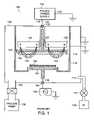
- FIG. 1illustrates a cross-sectional view of a known magnetron sputtering apparatus 100 having a pulsed power source 102 .
- the known magnetron sputtering apparatus 100includes a vacuum chamber 104 where the sputtering process is performed.
- the vacuum chamber 104is positioned in fluid communication with a vacuum pump 106 via a conduit 108 .
- the vacuum pump 106is adapted to evacuate the vacuum chamber 104 to high vacuum.
- the pressure inside the vacuum chamber 104is generally less than 100 Pa during operation.
- a feed gas source 109such as an argon gas source, is coupled to the vacuum chamber 104 by a gas inlet 110 .
- a valve 112controls the gas flow from the feed gas source 109 .
- the magnetron sputtering apparatus 100also includes a cathode assembly 114 having a target 116 .
- the cathode assembly 114is generally in the shape of a circular disk.
- the cathode assembly 114is electrically connected to a first output 118 of the pulsed power supply 102 with an electrical transmission line 120 .
- the cathode assembly 114is typically coupled to the negative potential of the pulsed power supply 102 .
- an insulator 122can be used to pass the electrical transmission line 120 through a wall of the vacuum chamber 104 .
- a grounded shield 124can be positioned behind the cathode assembly 114 to protect a magnet 126 from bombarding ions.
- the magnet 126 shown in FIG. 1is generally shaped in the form of a ring that has its south pole 127 on the inside of the ring and its north pole 128 on the outside of the ring. Many other magnet configurations can also be used.
- An anode 130is positioned in the vacuum chamber 104 proximate to the cathode assembly 114 .
- the anode 130is typically coupled to ground.
- a second output 132 of the pulsed power supply 102is also typically coupled to ground.
- a substrate 134is positioned in the vacuum chamber 104 on a substrate support 135 to receive the sputtered target material from the target 116 .
- the substrate 134can be electrically connected to a bias voltage power supply 136 with a transmission line 138 .
- an insulator 140can be used to pass the electrical transmission line 138 through a wall of the vacuum chamber 104 .
- the pulsed power supply 102applies a voltage pulse between the cathode assembly 114 and the anode 130 that has a sufficient amplitude to ionize the argon feed gas in the vacuum chamber 104 .
- the typical ionization processis referred to as direct ionization or atomic ionization by electron impact and can be described as follows: Ar+e ⁇ ⁇ Ar + +2e ⁇
- Arrepresents a neutral argon atom in the feed gas and e ⁇ represents an ionizing electron generated in response to the voltage pulse applied between the cathode assembly 114 and the anode 130 .
- the collision between the neutral argon atom and the ionizing electronresults in an argon ion (Ar + ) and two electrons.
- the negatively biased cathode assembly 114attracts positively charged ions with sufficient acceleration so that the ions sputter the target material from the target 116 .
- a portion of the sputtered target materialis deposited on the substrate 134 .
- Sputtering systemsare generally calibrated to determine the deposition rate under certain operating conditions.
- the erosion rate of the target 116can be expressed by the following equation:
- kis a constant
- jis the ion current density in mA/cm 2
- Yis the sputtering yield in atoms/ion
- Mis the atomic weight in grams
- ⁇is the density in gm/cm 3 of the target material.
- the deposition rateis generally proportional to the sputtering yield Y.
- FIG. 2illustrates a cross-sectional view of a prior art cathode assembly 114 ′ having a cathode cooling system.
- the cathode assembly 114 ′includes target 116 ′.
- the cathode cooling systemalso includes a conduit 150 that contains a fluid 152 for conducting heat away from the cathode assembly 114 ′.
- the fluid 152can be a liquid coolant or a gas, for example.
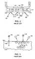
- FIG. 3illustrates a known process for sputtering material from a target 116 ′.
- An ion 154 having a mass M i and a velocity v iimpacts a target particle 162 having a mass M t which is initially at rest on the surface 156 of the target 116 ′.
- the ion 154impacts the surface 156 at normal incidence.
- the momentum from the ion 154transfers to the target particle 162 driving the target particle 162 into the target 116 ′.
- the ejection of a sputtered particle 164 from the target 114 ′generally requires a sequence of collisions for a component of the initial momentum vector to change by more than ninety degrees.
- an incident ion 154experiences a cascade of collisions and its energy is partitioned over a region of the target surface 156 .
- the sputtering momentum exchangeoccurs primarily within a region extending only about ten angstroms below the surface 156 .
- the incident ion 154generally strikes two lattice atoms 166 , 168 almost simultaneously. This low energy knock-on receives a side component of momentum and initiates sputtering of one or more of its neighbors.
- the primary knock-onis driven into the target 114 ′, where it can be reflected and sometimes returned to the surface 156 to produce sputtering by impacting the rear of a surface atom 170 .
- a fraction of the kinetic energy of the incident ion 154is transferred to the target particle 162 .
- This kinetic energy transfer functioncan be expressed as follows:
- the sputtering yield Ycan be expressed as follows, assuming perpendicular ion incidence onto a substantially planar surface 156 :
- ⁇is the energy transfer function
- ⁇is a near-linear function of the ratio of the mass of the target atom 162 to the mass of the incident ion 154
- Eis the kinetic energy of the incident ion 154
- Uis the surface binding energy for the target material.
- the mass dependence of ⁇does not vary greatly from one material to another.
- the primary material-sensitive factoris the surface binding energy, and this has only a first power dependence.
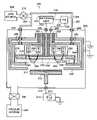
- FIG. 4illustrates a cross-sectional view of an embodiment of a magnetron sputtering apparatus 200 according to the present invention.
- the magnetron sputtering apparatus 200includes a chamber 202 , such as a vacuum chamber.
- the chamber 202is coupled in fluid communication to a vacuum system 204 through a vacuum valve 206 .
- the chamber 202is electrically coupled to ground potential.
- the chamber 202is coupled to a feed gas source 208 by one or more gas lines 207 .
- the gas lines 207are isolated from the chamber and other components by insulators 209 . Additionally, the gas lines 207 can be isolated from the feed gas source using in-line insulating couplers (not shown).
- a gas flow control system 210controls the gas flow to the chamber 202 .
- the gas source 208can contain any feed gas.
- the feed gascan be a noble gas or a mixture of noble gases.
- the feed gascan also be a reactive gas, a non-reactive gas, or a mixture of both reactive and non-reactive gases.
- the magnetron sputtering apparatus 200also includes a cathode assembly 216 .
- the cathode assembly 216includes a cathode 218 and a sputtering target 220 composed of target material.
- the cathode 218is formed of a metal.
- the cathode 218is formed of a chemically inert material, such as stainless steel.
- the sputtering target 220is in physical contact with the cathode 218 .
- the sputtering target 220is positioned inside the cathode 218 as shown in FIG. 4 .
- the distance from the sputtering target 220 to the substrate 211can vary from a few centimeters to about one hundred centimeters.
- the target materialcan be any material suitable for sputtering.
- the target materialcan be a metallic material, polymer material, superconductive material, magnetic material including ferromagnetic material, non-magnetic material, conductive material, non-conductive material, composite material, reactive material, or a refractory material.
- the cathode assembly 216is coupled to an output 222 of a matching unit 224 .
- An insulator 226isolates the cathode assembly 216 from a grounded wall of the chamber 202 .
- An input 230 of the matching unit 224is coupled to a first output 232 of a pulsed power supply 234 .
- a second output 236 of the pulsed power supply 234is coupled to an anode 238 .
- An insulator 240isolates the anode 238 from a grounded wall of the chamber 202 .
- Another insulator 242isolates the anode 238 from the cathode assembly 216 .
- the first output 232 of the pulsed power supply 234is directly coupled to the cathode assembly 216 .
- the second output 236 of the pulsed power supply 234 and the anode 238are both coupled to ground.
- the first output 232 of the pulsed power supply 234couples a negative voltage impulse to the cathode assembly 216 .
- the second output 236 of the pulsed power supply 234couples a positive voltage impulse to the anode 238 .
- the pulsed power supply 234generates peak voltage levels of between about 5 kV and about 30 kV. In one embodiment, operating voltages are generally between about 50V and 1 kV. In one embodiment, the pulsed power supply 234 sustains discharge current levels that are on order of about 1 A to 5,000 A depending on the volume of the plasma. Typical operating currents varying from less than about one hundred amperes to more than a few thousand amperes depending on the volume of the plasma. In one embodiment, the power pulses have a repetition rate that is below 1 kHz. In one embodiment, the pulse width of the pulses generated by the pulsed power supply 234 is substantially between about one microsecond and several seconds.
- the magnetron sputtering apparatus 200also includes a magnet assembly 252 .
- the magnet assembly 252is adapted to create a magnetic field 254 proximate to the cathode assembly 216 .
- the magnet assembly 252can include permanent magnets 256 , or alternatively, electro-magnets (not shown).
- the configuration of the magnet assembly 252can be varied depending on the desired shape and strength of the magnetic field 254 .
- the magnet assemblycan have either a balanced or unbalanced configuration.
- the magnet assembly 252includes switching electro-magnets, which generate a pulsed magnetic field proximate to the cathode assembly 216 .
- additional magnet assembliescan be placed at various locations around and throughout the chamber 202 to direct different types of sputtered target materials to the substrate 212 .
- the magnetron sputtering apparatus 200is operated by generating the magnetic field 254 proximate to the cathode assembly 216 .
- the permanent magnets 256continuously generate the magnetic field 254 .
- electro-magnets(not shown) generate the magnetic field 254 by energizing a current source that is coupled to the electro-magnets.
- the strength of the magnetic field 254is between about fifty gauss and two thousand gauss.
- the feed gasis supplied to the chamber 202 directly between the cathode assembly 216 and the anode 238 .
- Directly injecting the feed gas between the cathode assembly 216 and the anode 238can increase the flow rate of the gas between the cathode assembly 216 and the anode 238 .
- Increasing the flow rate of the gasallows longer duration impulses and thus, can result in the formation higher density plasmas.
- the flow of the feed gasis further discussed herein.
- the weakly-ionized plasmais also referred to as a pre-ionized plasma.
- the peak plasma density of the pre-ionized plasmais between about 10 6 and 10 12 cm ⁇ 3 for argon feed gas.
- the pressure in the chambervaries from about 10 ⁇ 3 to 10 Torr. The peak plasma density of the pre-ionized plasma depends on the properties of the specific plasma processing system.
- the pulsed power supply 234generates a low power pulse having an initial voltage that is between about 100V and 5 kV with a discharge current that is between about 0.1 A and 100 A in order to generate the weakly-ionized plasma.
- the width of the pulsecan be on the order of 0.1 microseconds to one hundred seconds. Specific parameters of the pulse are discussed herein in more detail.
- the pulsed power supply 234applies a voltage between the cathode assembly 216 and the anode 238 before the feed gas is supplied between the cathode assembly 216 and the anode 238 . In another embodiment, the pulsed power supply 234 applies a voltage between the cathode assembly 216 and the anode 238 after the feed gas is supplied between the cathode assembly 216 and the anode 238 .
- a direct current (DC) power supply(not shown) is used to generate and maintain the weakly-ionized or pre-ionized plasma.
- the DC power supplyis adapted to generate a voltage that is large enough to ignite the pre-ionized plasma.
- the DC power supplygenerates an initial voltage of several kilovolts between the cathode assembly 216 and the anode 238 in order to generate and maintain the pre-ionized plasma.
- the initial voltage between the cathode assembly 216 and the anode 238creates a plasma discharge voltage that is on the order of 100V to 1000V with a discharge current that is on the order of 0.1 A to 100 A.
- the direct current required to generate and maintain the pre-ionized plasmais a function of the volume of the plasma.
- the current required to generate and maintain the pre-ionized plasmais a function of the strength of the magnetic field in the region 245 .
- the DC power supplygenerates a current that is on order of 1 mA to 100 A depending on the volume of the plasma and the strength of the magnetic field in the region 245 .
- the DC power supplycan be adapted to generate and maintain an initial peak voltage between the cathode assembly 216 and the anode 238 before the introduction of the feed gas.
- an alternating current (AC) power supply(not shown) is used to generate and maintain the weakly-ionized or pre-ionized plasma.
- the weakly-ionized or pre-ionized plasmacan be generated and maintained using electron cyclotron resonance (ECR), capacitively coupled plasma discharge (CCP), or inductively coupled plasma (ICP) discharge.
- ECRelectron cyclotron resonance
- CCPcapacitively coupled plasma discharge
- ICPinductively coupled plasma
- AC power suppliescan require less power to generate and maintain a weakly-ionized plasma than a DC power supply.
- the pre-ionized or weakly-ionized plasmacan be generated by numerous other techniques, such as UV radiation techniques, X-ray techniques, electron beam techniques, ion beam techniques, or ionizing filament techniques.
- the weakly-ionized plasmais formed outside of the region 245 and then diffuses into the region 245 .
- Forming a weakly-ionized or pre-ionized plasmasubstantially eliminates the probability of establishing a breakdown condition in the chamber 202 when high-power pulses are applied between the cathode assembly 216 and the anode 238 .
- Uniformly distributing the weakly-ionized or pre-ionized plasma over the cathode arearesults in a more uniform strongly ionized plasma when a high power pulse is applied.
- the probability of establishing a breakdown conditionis substantially eliminated because the weakly-ionized plasma has a low-level of ionization that provides electrical conductivity through the plasma. This conductivity greatly reduces or prevents the possibility of a breakdown condition when high power is applied to the plasma.
- high-power pulsesare then generated between the cathode assembly 216 and the anode 238 .
- the pulsed power supply 234generates the high-power pulses.
- the desired power level of the high-power pulsedepends on several factors including the desired deposition rate, the density of the pre-ionized plasma, and the volume of the plasma, for example. In one embodiment, the power level of the high-power pulse is in the range of about 1 kW to about 10 MW.
- the high-power pulsesare rapidly applied across the weakly-ionized plasma.
- the high-power pulsesare substantially instantly applied across the weakly-ionized plasma in a substantially explosive manner. This rapid application of the high-power pulses can result in a surface layer of the target 220 being almost instantly evaporated.
- Each of the high-power pulsesare maintained for a predetermined time that, in one embodiment, is in the range of about one microsecond to about ten seconds. In one embodiment, the repetition frequency or repetition rate of the high-power pulses is in the range of between about 0.1 Hz to 1 kHz. In order to minimize undesirable substrate heating, the average power generated by the pulsed power supply 234 can be less than one megawatt depending on the volume of the plasma.
- the high-power pulseis applied so rapidly that a surface layer of the target 220 is substantially vaporized and only a small quantity of heat is conducted through the cathode assembly 216 .
- the thermal energy in at least one of the cathode assembly 216 , the anode 238 , and the substrate support 212is conducted away or dissipated by liquid or gas cooling such as helium cooling (not shown).
- the high-power pulsesgenerate a strong electric field between the cathode assembly 216 and the anode 238 .
- This strong electric fieldis substantially located in the region 245 across the gap 244 between the cathode assembly 216 and the anode 238 .
- the electric fieldis a pulsed electric field.
- the electric fieldis a quasi-static electric field.
- the term “quasi-static electric field”is defined herein to mean an electric field that has a characteristic time of electric field variation that is much greater than the collision time for electrons with neutral gas particles. Such a time of electric field variation can be on the order of ten seconds. The strength and the position of the strong electric field will be discussed in more detail herein.
- the high-power pulsesgenerate a highly-ionized or a strongly-ionized plasma from the weakly-ionized plasma.
- the discharge current that is formed from this strongly-ionized plasmacan be on the order of 5 kA for a pressure that is on the order of about 100 mTorr and 10 Torr.
- the positively charged ions in the strongly-ionized plasmaaccelerate at high velocity towards the sputtering target 220 .
- the accelerated ionsimpact the surface of the sputtering target 220 , causing the target material to be sputtered.
- the strongly-ionized plasma of the present inventionresults in a very high sputtering rate of the target material.
- the strongly-ionized plasmatends to diffuse homogenously in the region 246 and, therefore tends to create a more homogeneous plasma volume.
- the homogenous diffusionresults in accelerated ions impacting the surface of the sputtering target 220 in a more uniform manner than with conventional magnetron sputtering. Consequently, the surface of the sputtering target 220 is eroded more evenly and, thus higher target utilization is achieved.
- the target materialis sputtered more uniformly across the surface of the sputtering target 220 , the uniformity and homogeneity of the material deposited on the substrate 211 is also increased without the necessity of rotating the substrate 211 and/or the magnet assembly 252 .
- the high-power pulsed magnetron sputtering system 200 of the present inventiongenerates a relatively high electron temperature plasma and a relatively high density plasma.
- One application for the high-power pulsed magnetron sputtering system 200 of the present inventionis ionized physical vapor deposition (IPVD), which is a technique that converts neutral sputtered atoms into positive ions in order to enhance the sputtering process.
- IPVDionized physical vapor deposition
- FIG. 5A through FIG. 5Dillustrate cross-sectional views of the sputtering apparatus 200 having the pulsed power supply 234 .
- FIG. 5Aillustrates a cross-sectional view of the sputtering apparatus 200 having the pulsed power supply 234 at a time before the pulsed power supply 234 is activated.
- FIG. 5Aillustrates the cathode assembly 216 including the sputtering target 220 .
- the cathode assembly 216is coupled to the output 222 of the matching unit 224 .
- the input 230 of the matching unit 224is coupled to the first output 232 of the pulsed power supply 234 .
- the second output 236 of the pulsed power supply 234is coupled to the anode 238 .
- the anode 238is positioned so as to form a gap 244 between the anode 238 and the cathode assembly 216 that is sufficient to allow current to flow through the region 245 between the anode 238 and the cathode assembly 216 .
- the width of the gap 244is between approximately 0.3 cm and 10 cm.
- the surface area of the cathode assembly 216determines the volume of the region 245 .
- the gap 244 and the total volume of the region 245are parameters in the ionization process as described herein.
- the gas lines 207provide feed gas 256 from the feed gas source 208 ( FIG. 4 ) proximate to the anode 238 and the cathode assembly 216 .
- the feed gas 256 from the gas source 208is supplied by the gas flow control system 210 ( FIG. 4 ).
- the feed gas 256is supplied between the cathode assembly 216 and the anode 238 .
- Directly injecting the feed gas 256 between the cathode assembly 216 and the anode 238can increase the flow rate of the feed gas 256 .
- Thiscauses a rapid volume exchange in the region 245 between the cathode assembly 216 and the anode 238 , which permits a high power pulse having a longer duration to be applied across the gap 244 .
- the longer duration high power pulseresults in the formation of more dense plasma. This volume exchange is described herein in more detail.
- FIG. 5Billustrates the cathode assembly 216 after the feed gas 256 is supplied between the cathode assembly 216 and the anode 238 .
- the pulsed power supply 234applies a voltage pulse between the cathode assembly 216 and the anode 238 .
- the pulsed power supply 234applies a negative voltage pulse to the cathode assembly 216 .
- the characteristics of the voltage pulseare chosen such that an electric field 260 develops between the cathode assembly 216 and the anode 238 that creates a weakly-ionized plasma 262 in the region 245 between the anode 238 and the cathode assembly 216 .
- the weakly-ionized plasma 262is also referred to as a pre-ionized plasma.
- the pulsed power supply 234generates the weakly-ionized plasma 262 by generating a low power pulse having an initial voltage that is in the range of 100V to 5 kV with a discharge current that is in the range of 0.1 A to 100 A.
- the width of the pulsecan be in the range of 0.1 microseconds to one hundred seconds. Specific parameters of the pulse are discussed herein in more detail.
- an alternating current (AC) power supply(not shown) is used to generate and maintain the weakly-ionized or pre-ionized plasma 262 .
- the weakly-ionized or pre-ionized plasma 262can be generated and maintained using electron cyclotron resonance (ECR), capacitively coupled plasma discharge (CCP), or inductively coupled plasma (ICP) discharge.
- ECRelectron cyclotron resonance
- CCPcapacitively coupled plasma discharge
- ICPinductively coupled plasma
- the pre-ionized or weakly-ionized plasma 262can be generated by numerous other techniques, such as UV radiation techniques, X-ray techniques, electron beam techniques, ion beam techniques, or ionizing filament techniques. These techniques include components used in ionization sources according to the invention.
- the weakly-ionized plasmais formed outside of the region 245 and then diffuses into the region 245 .
- the weakly-ionized plasma 262diffuses generally in a homogeneous manner through the region 264 .
- the homogeneous diffusiontends to facilitate the creation of a highly uniform strongly-ionized plasma in the region 264 .
- the weakly-ionized plasma 262is trapped proximate to the cathode assembly 216 by a magnetic field. Specifically, electrons in the weakly-ionized plasma 262 are trapped by a magnetic field generated proximate to the cathode assembly 216 .
- the strength of the magnetic fieldis in the range of fifty to two thousand gauss.
- the pulsed power supply 234generates high-power pulses between the cathode assembly 216 and the anode 238 ( FIG. 5C ) after the weakly-ionized plasma 262 is formed.
- the desired power level of the high-power pulsesdepends on several factors including the density of the weakly-ionized plasma 262 and the volume of the plasma. In one embodiment, the power level of the high-power pulse is in the range of about 1 kW to about 10 MW or higher.
- the high-power pulsesgenerate a strong electric field 266 between the cathode assembly 216 and the anode 238 .
- the strong electric field 266is substantially located in the region 245 between the cathode assembly 216 and the anode 238 .
- the electric field 266is a pulsed electric field.
- the electric field 266is a quasi-static electric field. The strength and the position of the strong electric field 266 will be discussed in more detail herein.
- FIG. 5Dillustrates the high-power pulses generating a highly-ionized or a strongly-ionized plasma 268 from the weakly-ionized plasma 262 .
- the strongly-ionized plasma 268is also referred to as a high-density plasma.
- the discharge current that is formed from the strongly-ionized plasma 268can be on the order of about 1,000 A or more with a discharge voltage in the range of 50V to 1,000V for a pressure that is in the range of 5 mTorr and 10 Torr.
- the strongly-ionized plasma 268tends to diffuse homogenously in the region 264 . The homogenous diffusion creates a more homogeneous plasma volume.
- the homogenous diffusionresults in accelerated ions 272 in the strongly-ionized plasma 268 impacting the surface of the sputtering target 220 in a more uniform manner than with conventional magnetron sputtering. Consequently, the surface of the sputtering target 220 is eroded more evenly and, thus higher target utilization is achieved. Furthermore, since the target material is sputtered more uniformly across the surface of the sputtering target 220 , the target material is deposited more uniformly on the substrate 211 ( FIG. 4 ) without the necessity of rotating the substrate and/or the magnetron.
- the strong electric field 266facilitates a multi-step ionization process of the feed gas 256 that substantially increases the rate at which the strongly-ionized plasma 268 is formed.
- the multi-step or stepwise ionization processis described as follows.
- a pre-ionizing voltageis applied between the cathode assembly 216 and the anode 238 across the feed gas 256 , which forms the weakly-ionized plasma 262 .
- the weakly-ionized plasma 262is generally formed in the region 245 and diffuses to the region 264 as the feed gas 256 continues to flow.
- a magnetic field 254( FIG. 4 ) is generated in the region 245 and extends to the center of the cathode assembly 216 . This magnetic field tends to assist in diffusing electrons from the region 245 to the region 264 .
- the electrons in the weakly-ionized plasma 262are substantially trapped in the region 264 by the magnetic field 245 .
- the volume of weakly-ionized plasma 262 in the region 245is rapidly exchanged with a fresh volume of feed gas 256 .
- the pulsed power supply 234applies a high-power pulse between the cathode assembly 216 and the anode 238 after the formation of the weakly-ionized plasma 262 ( FIG. 2C ).
- This high-power pulsegenerates the strong electric field 266 in the region 245 between the cathode assembly 216 and the anode 238 .
- the strong electric field 266results in collisions occurring between neutral atoms 270 , electrons (not shown), and ions 272 in the weakly-ionized plasma 262 . These collisions generate numerous excited atoms 274 in the weakly-ionized plasma 262 .
- the accumulation of excited atoms 274 in the weakly-ionized plasma 262alters the ionization process.
- the strong electric field 266facilitates a multi-step ionization process of an atomic feed gas that significantly increases the rate at which the strongly-ionized plasma 268 is formed.
- the multi-step ionization processhas an efficiency that increases as the density of excited atoms 274 in the weakly-ionized plasma 262 increases.
- the strong electric field 266enhances the formation of ions of a molecular or atomic feed gas.
- the distance or gap 244 between the cathode assembly 216 and the anode 238is chosen so as to maximize the rate of excitation of the atoms.
- the value of the electric field 266 in the region 245depends on the voltage level applied by the pulsed power supply 234 and the dimensions of the gap 244 between the anode 238 and the cathode assembly 216 .
- the strength of the electric field 266is in range of 10V/cm to 10 5 V/cm depending on various system parameters and operating conditions of the plasma system.
- the gap 244is in the range of 0.30 cm to 10 cm depending on various parameters of the desired plasma.
- the electric field 266 in the region 245is rapidly applied to the pre-ionized or weakly-ionized plasma 262 .
- the rapidly applied electric field 266is generated by applying a voltage pulse having a rise time that is in the range of 0.1 microsecond to ten seconds.
- the dimensions of the gap 244 and the parameters of the applied electric field 266are varied to determine the optimum condition for a relatively high rate of excitation of the atoms 270 in the region 245 .
- an argon atomrequires an energy of about 11.55 eV to become excited.
- the weakly-ionized plasma 262is formed and the atoms 270 in the weakly-ionized plasma 262 experience a stepwise ionization process.
- the excited atoms 274 in the weakly-ionized plasma 262then encounter the electrons (not shown) that are in the region 264 .
- the excited atoms 274only require about 4 eV of energy to ionize while neutral atoms 270 require about 15.76 eV of energy to ionize. Therefore, the excited atoms 274 will ionize at a much higher rate than the neutral atoms 270 .
- ions 272 in the strongly-ionized plasma 268strike the cathode assembly 216 causing secondary electron emission. These secondary electrons interact with neutral 270 or excited atoms 274 in the strongly-ionized plasma 268 . This process further increases the density of ions 272 in the strongly-ionized plasma 268 as the feed gas 256 is replenished.
- the multi-step ionization process corresponding to the rapid application of the electric field 266can be described as follows: Ar+e ⁇ ⁇ Ar*+e ⁇ Ar+e ⁇ ⁇ Ar + +2e ⁇
- the excited argon atoms 274generally require less energy to become ionized than neutral argon atoms 270 .
- the excited atoms 274tend to more rapidly ionize near the surface of the cathode assembly 216 than the neutral argon atoms 270 .
- the efficiency of the ionization processrapidly increases. This increased efficiency eventually results in an avalanche-like increase in the density of the strongly-ionized plasma 268 .
- the proportion of the energy applied to the weakly-ionized plasma 262 that is transformed to the excited atoms 274is very high for a pulsed discharge in the feed gas 256 .
- high power pulsesare applied to a weakly-ionized plasma 262 across the gap 244 to generate the strong electric field 266 between the anode 238 and the cathode assembly 216 .
- This strong electric field 266generates excited atoms 274 in the weakly-ionized plasma 262 .
- the excited atoms 274are rapidly ionized by secondary electrons emitted by the cathode assembly 216 .
- This rapid ionizationresults in a strongly-ionized plasma 268 having a large ion density being formed in the area 264 proximate to the cathode assembly 216 .
- the strongly-ionized plasma 268is also referred to as a high-density plasma.
- a higher density plasmais generated by controlling the flow of the feed gas 256 in the region 245 .
- a first volume of feed gas 256is supplied to the region 245 .
- the first volume of feed gas 256is then ionized to form a weakly-ionized plasma 262 in the region 245 .
- the pulsed power supply 234applies a high power electrical pulse across the weakly-ionized plasma 262 .
- the high power electrical pulsegenerates a strongly-ionized plasma 268 from the weakly-ionized plasma 262 .
- the level and duration of the high power electrical pulseis limited by the level and duration of the power that the strongly-ionized plasma 268 can absorb before the high power discharge contracts and terminates.
- the strength and the duration of the high-power electrical pulseare increased and thus the density of the strongly-ionized plasma 268 is increased by increasing the flow rate of the feed gas 256 .
- the strongly-ionized plasma 268is transported through the region 245 by a rapid volume exchange of feed gas 256 .
- feed gas 256moves through the region 245 , it interacts with the moving strongly-ionized plasma 268 and also becomes strongly-ionized from the applied high-power electrical pulse.
- the ionization processcan be a combination of direct ionization and/or stepwise ionization as described herein. Transporting the strongly-ionized plasma 268 through the region 245 by a rapid volume exchange of the feed gas 256 increases the level and the duration of the power that can be applied to the strongly-ionized plasma 268 and, thus, generates a higher density strongly-ionized plasma in the region 264 .
- a magnetic field(not shown) can be generated proximate to the cathode assembly 216 .
- the magnetic fieldsubstantially traps electrons in the weakly-ionized plasma 262 and secondary electrons from the cathode assembly 216 proximate to the cathode assembly 216 .
- the trapped electronsionize the excited atoms 274 generating the strongly-ionized plasma 268 .
- the magnetic fieldis generated in the region 245 to substantially trap electrons in the area where the weakly-ionized plasma 262 is ignited.
- a strongly-ionized plasma 268is used to sputter magnetic materials.
- Conventional magnetron sputteringgenerally is not suitable for sputtering magnetic materials, since the magnetic field generated by the magnetron can be absorbed by the magnetic target.
- Traditional RF diode sputteringcan be used to sputter magnetic materials. However, this method generally results in very poor uniformity of the sputtered film, relatively low plasma density, and relatively low deposition rate.
- magnetic materialscan be sputtering by driving a target assembly including a magnetic target material with a RF power supply (not shown).
- the RF power supplycan provide a power of up to about 10 kW.
- a substantially uniform weakly-ionized plasmacan be generated by applying RF power across a feed gas that is located proximate to the target assembly.
- the strongly-ionized plasmais generated by applying a strong electric field across the weakly-ionized plasma as described herein. Since the RF power supply applies a negative voltage bias to the target assembly, ions in the strongly-ionized plasma bombard the target material causing sputtering.
- a strongly-ionized plasma 268 according to the present inventionis used to sputter dielectric materials.
- Dielectric materialsare sputtered according to the present invention by driving a target assembly including a dielectric target material with a RF power supply (not shown).
- the RF power supplycan provide a power of up to about 10 kW.
- a substantially uniform weakly-ionized plasmacan be generated by applying RF power across a feed gas that is located proximate to the target assembly.
- a magnetic fieldcan be generated proximate to the target assembly in order to trap electrons in the weakly-ionized plasma.
- the strongly-ionized plasmais generated by applying a strong electric field across the weakly-ionized plasma as described herein. Since the RF power supply applies a negative voltage bias to the target assembly, ions in the strongly-ionized plasma bombard the target material causing sputtering.
- a DC power supply(not shown) is used to create a weakly-ionized plasma 232 for sputtering a dielectric target material according to the present invention.
- the dielectric target materialis positioned relative to the cathode 218 such that an area of the cathode 218 can conduct a direct current between the anode 238 and the cathode 218 .
- FIG. 6illustrates graphical representations 320 , 322 , and 324 of the absolute value of applied voltage, current, and power, respectively, as a function of time for periodic pulses applied to the plasma in the sputtering apparatus 200 of FIG. 4 .
- the feed gas 256flows proximate to the cathode assembly 216 before the pulsed power supply 234 is activated.
- the time required for a sufficient quantity of feed gas 256 to flow proximate to the cathode assembly 216depends on several factors including the flow rate of the feed gas 256 and the desired pressure in the region 245 .
- the power supply 234generates a constant power.
- the pulsed power supply 234generates a voltage 326 across the anode 238 and the cathode assembly 216 .
- the voltage 326is approximately between 100V and 5 kV.
- the period between time t 0 and time t 1can be on the order of several microseconds up to several milliseconds.
- the current 328 and the power 330have constant values.
- the voltage 326 at time t 2is in the range of 100V to 5 kV.
- the current 334 at time t 2is in the range of 0.1 A to 100 A.
- the power 336 delivered at time t 2is in the range of 0.01 kW to 100 kW.
- the period between time t 1 and time t 2is in the range of one microsecond to one hundred seconds to allow the pre-ionized plasma 262 to form and be maintained at a sufficient plasma density.
- the power 336 from the pulsed power supply 234is continuously applied in order to maintain the weakly-ionized plasma 262 .
- the pulsed power supply 234can be designed so as to output a continuous nominal power in order to sustain the weakly-ionized plasma 262 .
- the pulsed power supply 234delivers a large voltage pulse 338 across the weakly-ionized plasma 262 .
- the large voltage pulse 338has a voltage that is in the range of 200V to 30 kV.
- the period between time t 2 and time t 3is in the range of 0.1 microsecond to ten seconds.
- the large voltage pulse 338is applied before the current across the weakly-ionized plasma 262 begins to increase.
- the period between time t 3 and time t 4can be between about ten nanoseconds and one microsecond.
- time t 4 and time t 5the voltage 340 drops as the current 342 increases.
- the power 344also increases between time t 4 and time t 5 , until a quasi-stationary state exists between the voltage 346 and the current 348 .
- the period between time t 4 and time t 5is on order of several hundreds nanoseconds.
- the pulsed power supply 234delivers a high power pulse having a maximum power 350 and a pulse width that is sufficient to transform the weakly-ionized plasma 262 to a strongly-ionized plasma 268 (see FIG. 2D ). At time t 6 , the maximum power 350 is terminated. In one embodiment, the pulsed power supply 234 continues to supply a background power that is sufficient to maintain the plasma after time t 6 .
- the power supply 234generates a constant voltage.
- the applied voltage 320is continuously applied from time t 2 until time t 6 .
- the current 322 and the power 324rise until time t 6 where they maintain a constant voltage level, and then the voltage 320 is terminated.
- the values for the current, power and voltageare optimized for generating exited atoms.
- the efficiency of the ionization processis increased by generating a magnetic field proximate to the cathode assembly 216 .
- the magnetic fieldsubstantially traps electrons in the weakly-ionized plasma 262 proximate to the cathode assembly 216 .
- the trapped electronsionize the excited atoms 274 thereby generating the strongly-ionized plasma 268 .
- the magnetically enhanced plasmahas strong diamagnetic properties.
- strong diamagnetic propertiesis defined herein to mean that the magnetically enhanced high-density plasma discharge tends to exclude external magnetic fields from the plasma volume.
- FIG. 7A through FIG. 7Dillustrate various simulated magnetic field distributions 400 , 402 , 404 , and 406 proximate to the cathode assembly 216 for various electron ExB drift currents in a magnetically enhanced plasma sputtering apparatus according to the invention.
- the magnetically enhanced plasma generating apparatusincludes a magnet assembly 252 that is positioned proximate to the cathode assembly 216 .
- the magnet assembly 252generates a magnetic field proximate to the cathode assembly 216 .
- the strength of the magnetic fieldis in the range of fifty to two thousand gauss.
- the simulated magnetic fields distributions 400 , 402 , 404 , and 406indicate that high-power plasmas having high current density tend to diffuse homogeneously in an area 246 of the magnetically enhanced plasma sputtering apparatus.
- the high-power pulses applied between the cathode assembly 216 and the anode 238generate secondary electrons from the cathode assembly 216 that move in a substantially circular motion proximate to the cathode assembly 216 according to crossed electric and magnetic fields.
- the substantially circular motion of the electronsgenerates an electron ExB drift current.
- the magnitude of the electron ExB drift currentis proportional to the magnitude of the discharge current in the plasma and, in one embodiment, is approximately in the range of three to ten times the magnitude of the discharge current.
- the electron ExB drift currentdefines a substantially circular shape for a low current density plasma.
- the substantially circular electron ExB drift currenttends to describe a more complex shape as the interaction of the magnetic field generated by the magnet assembly 252 , the electric field generated by the high-power pulse, and the magnetic field generated by the electron ExB drift current become more acute.
- the electron ExB drift currenthas a substantially cycloidal shape.
- the exact shape of the electron ExB drift currentcan be complex and depends on various factors.
- the electron ExB drift current 410is in the range of three to ten times as great as the discharge current.
- the discharge currentis in the range of 10 A to 30 A.
- the magnetic field lines 408 shown in FIG. 7Aindicate that the magnetic field generated by the magnet assembly 252 is substantially undisturbed by the relatively small magnetic field that is generated by the relatively small electron ExB drift current 410 .
- the magnetic field lines 418 that are generated by the magnet assembly 252exhibit substantial distortion that is caused by the relatively strong magnetic field generated by the relatively large electron ExB drift current 420 .
- the larger electron ExB drift current 420generates a stronger magnetic field that strongly interacts with and can begin to dominate the magnetic field generated by the magnet assembly 252 .
- FIG. 7Dillustrates the magnetic field lines 424 produced from the interaction of the magnetic field generated by the magnet assembly 252 and the magnetic field generated by an electron ExB drift current 426 .
- the electron ExB drift current 426is generated proximate to the cathode assembly 216 .
- the electron ExB drift current 426is approximately 5 kA.
- the discharge current in this exampleis approximately between 500 A and 1,700 A.
- the magnetic field lines 424 generated by the magnet assembly 252exhibit relatively high distortion due to their interaction with the relatively strong magnetic field generated by the relatively large electron ExB drift current 426 .
- the relatively large electron ExB drift current 426generates a very strong magnetic field that is substantially stronger than the magnetic field generated by the magnet assembly 252 .
- the present inventiongenerates a very high discharge current and a very high sputtering yield.
- the high-power pulseis applied almost instantaneously, causing an explosive reaction at the surface of the target.
- the explosive reactionrapidly vaporizes a surface layer of the target.
- FIG. 8illustrates a graphical representation 500 of sputtering yield Y as a function of temperature T of the sputtering target 220 of FIG. 4 .
- a higher deposition ratecan be achieved according to the present invention by using a thermal sputtering process.
- the deposition rateis increased by increasing the sputtering yield.
- the sputtering yield of the target 220is increased as the temperature of the target 220 is increased.
- the sputtering yieldslowly increases in a substantially linear manner as shown in region 502 . In the region 502 , the sputtering yield generally does not depend on the temperature of the target 220 .
- the sputtering yieldincreases at a non-linear rate. In one embodiment, the sputtering yield increases at an exponential rate.
- the temperature T 0is approximately equal to 0.7 T m , where T m is the melting point of the target material. In another embodiment, the temperature T 0 is approximately equal to U/40 k, where U is the binding energy for a surface atom and k is Boltzman's constant.
- ⁇ T Mis the maximum difference of the target temperature from the temperature T 0
- Ris the initial radius of the high temperature area on the target
- ⁇is the time period for the high temperature in the high temperature area
- ⁇is the coefficient for the temperature conductivity
- Uis the binding energy
- the sputtering yieldincreases non-linearly. In one embodiment, the sputtering yield increases substantially in an exponential manner.
- a high power pulseis applied to a weakly-ionized plasma 262 ( FIG. 5C ) for a relatively short duration. This high power pulse creates a strongly-ionized plasma 268 ( FIG. 5D ) that contains a high density of energetic ions 272 .
- FIG. 9illustrates a process 510 for sputtering atoms 512 from a target 220 according one embodiment of the invention.
- the target 220is negatively biased.
- the negative biascauses the energetic ions 272 in the strongly-ionized plasma 268 to vigorously impact the surface 514 of the target 220 , thereby causing the temperature of the target to rapidly increase.
- the sputtering yieldincreases nonlinearly.
- the sputtering yieldincreases almost exponentially. Consequently, the deposition rate rapidly increases.
- the sputtering yieldcan depend on the properties of the target material, such as the crystal structure, the binding energy of the surface atoms, and/or the melting point of the target material.
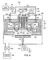
- FIG. 10illustrates a cross-sectional view of a cathode assembly 216 according to one embodiment of the invention.
- the target materialis evaporated in an avalanche-like manner.
- the high-power pulsegenerates thermal energy 516 into only a shallow depth of the target 220 so as to not substantially increase an average temperature of the target 220 .
- the target materialis almost instantly evaporated. However damage to the target 220 itself is minimal because thermal energy only penetrates into the shallow skin depth.
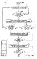
- FIG. 11is a flowchart 600 of an illustrative process of enhancing a sputtering yield of a sputtering target according to the present invention.
- the processis initiated (step 602 ) by pumping the chamber 202 down to a specific pressure (step 604 ).
- the pressure in the chamberis evaluated (step 606 ).
- a feed gasis then pumped into the chamber (step 608 ).
- the gas pressureis evaluated (step 610 ). If the gas pressure is correct, the pressure in the chamber is again evaluated (step 612 ).
- an appropriate magnetic field 254( FIG. 4 ) can be generated proximate to the feed gas 256 ( FIG. 5B ) (step 614 ).
- a magnet assembly 252can include at least one permanent magnet, and thus the magnetic field is generated constantly, even before the process is initiated.
- a magnetic assembly 252includes at least one electromagnet, and thus the magnetic field is generated only when the electromagnet is operating. In one embodiment, the magnetic field 254 is then evaluated (step 616 ).
- the feed gas 256is ionized to generate a weakly-ionized plasma 262 (step 618 ).
- the weakly-ionized plasma 262is generated by creating a relatively low current discharge in the gap 244 between the cathode assembly 216 and the anode 238 .
- the weakly-ionized plasma 262can be generated by creating a relatively low current discharge between an ionizing electrode and the cathode assembly 216 .
- an electrodeis heated to emit electrons proximate to the cathode assembly 216 .
- a relatively low current dischargeis created between the anode 238 and the electrode in order to generate the weakly-ionized plasma 262 .
- the weakly-ionized plasma 262is generated by applying a potential across the gap 244 between the cathode assembly 216 and the anode 238 after the introduction of the feed gas 256 .
- a strongly-ionized plasma 268( FIG. 5D ) is generated from the weakly-ionized plasma 262 (step 622 ).
- the strongly-ionized plasma 268is generated by applying a high-power pulse between the cathode assembly 216 and the anode 238 . As described herein, the high-power pulse causes a strong electric field 266 to be generated in the gap 244 between the anode 238 and the cathode assembly 216 .
- the strong electric field 266causes the feed gas to experience stepwise ionization.
- the feed gasincludes a molecular gases and the strong electric field 266 increases the formation of ions that enhance the strongly-ionized plasma 268 .
- the strongly-ionized plasma 268is substantially homogeneous in the area 264 of FIG. 5D . This homogeneity results in more uniform erosion of the sputtering target 220 and, therefore, relatively high target utilization. Since the cathode assembly 216 is negatively biased relative to the anode 238 , the cathode assembly 216 attracts ions from the strongly-ionized substantially uniform plasma. This causes the ions to bombard the cathode assembly 216 , thereby resulting in sputtering of the target material.
- the strongly-ionized plasmais enhanced through the rapid exchange of the strongly-ionized plasma with a fresh volume of feed gas 256 (step 624 ). This rapid exchange occurs in the region 245 . In one embodiment, the rapid exchange of the strongly-ionized plasma occurs during the duration of the high-power pulse.
- the sputtering yieldis monitored (step 628 ) by known monitoring techniques. If the sputtering yield is insufficient (step 630 ), the power delivered to the plasma is increased (step 632 ). In one embodiment, increasing the magnitude of the high-power pulse applied between the cathode assembly 216 and the anode 238 increases the power delivered to the plasma. In one embodiment, the power delivered to the plasma is sufficient to vaporize a surface layer of the target. This increases the sputtering yield in a substantially nonlinear fashion.
- the sputter yieldis again evaluated (step 628 ). This process continues until the sputter yield is sufficient (step 630 ), and sputtering continues (step 634 ). Once the sputter deposition is completed (step 636 ), the sputter process is terminated (step 638 ).
Landscapes
- Chemical & Material Sciences (AREA)
- Engineering & Computer Science (AREA)
- Physics & Mathematics (AREA)
- Plasma & Fusion (AREA)
- Analytical Chemistry (AREA)
- Chemical Kinetics & Catalysis (AREA)
- Materials Engineering (AREA)
- Mechanical Engineering (AREA)
- Metallurgy (AREA)
- Organic Chemistry (AREA)
- Optics & Photonics (AREA)
- Condensed Matter Physics & Semiconductors (AREA)
- General Physics & Mathematics (AREA)
- Manufacturing & Machinery (AREA)
- Computer Hardware Design (AREA)
- Microelectronics & Electronic Packaging (AREA)
- Power Engineering (AREA)
- Physical Vapour Deposition (AREA)
- Inorganic Compounds Of Heavy Metals (AREA)
- Plasma Technology (AREA)
- Coating By Spraying Or Casting (AREA)
- Disintegrating Or Milling (AREA)
Abstract
Description
Ar+e−→Ar++2e−
Ar+e−→Ar*+e−
Ar+e−→Ar++2e−
- where Ar represents a
neutral argon atom 270 in thefeed gas 256 and e− represents an ionizing electron generated in response to apre-ionized plasma 262, when sufficient voltage is applied between thecathode assembly 216 and theanode 238. Additionally, Ar* represents anexcited argon atom 274 in the weakly-ionizedplasma 262. The collision between theexcited argon atom 274 and the ionizing electron results in an argon ion (Ar+) and two electrons.
- where Ar represents a
RD=K×Y×I
Claims (48)
Priority Applications (3)
| Application Number | Priority Date | Filing Date | Title |
|---|---|---|---|
| US11/183,463US7811421B2 (en) | 2002-11-14 | 2005-07-18 | High deposition rate sputtering |
| US12/879,036US20100326815A1 (en) | 2002-11-14 | 2010-09-10 | High Power Pulse Ionized Physical Vapor Deposition |
| US15/219,975US20170029936A1 (en) | 2002-11-14 | 2016-07-26 | High power pulse ionized physical vapor deposition |
Applications Claiming Priority (3)
| Application Number | Priority Date | Filing Date | Title |
|---|---|---|---|
| US10/065,739US6896773B2 (en) | 2002-11-14 | 2002-11-14 | High deposition rate sputtering |
| US11/091,814US20050178654A1 (en) | 2002-11-14 | 2005-03-28 | High deposition rate sputtering |
| US11/183,463US7811421B2 (en) | 2002-11-14 | 2005-07-18 | High deposition rate sputtering |
Related Parent Applications (1)
| Application Number | Title | Priority Date | Filing Date |
|---|---|---|---|
| US11/091,814ContinuationUS20050178654A1 (en) | 2002-11-14 | 2005-03-28 | High deposition rate sputtering |
Related Child Applications (1)
| Application Number | Title | Priority Date | Filing Date |
|---|---|---|---|
| US12/879,036ContinuationUS20100326815A1 (en) | 2002-11-14 | 2010-09-10 | High Power Pulse Ionized Physical Vapor Deposition |
Publications (2)
| Publication Number | Publication Date |
|---|---|
| US20050252763A1 US20050252763A1 (en) | 2005-11-17 |
| US7811421B2true US7811421B2 (en) | 2010-10-12 |
Family
ID=32296386
Family Applications (5)
| Application Number | Title | Priority Date | Filing Date |
|---|---|---|---|
| US10/065,739Expired - LifetimeUS6896773B2 (en) | 2002-11-14 | 2002-11-14 | High deposition rate sputtering |
| US11/091,814AbandonedUS20050178654A1 (en) | 2002-11-14 | 2005-03-28 | High deposition rate sputtering |
| US11/183,463Expired - Fee RelatedUS7811421B2 (en) | 2002-11-14 | 2005-07-18 | High deposition rate sputtering |
| US12/879,036AbandonedUS20100326815A1 (en) | 2002-11-14 | 2010-09-10 | High Power Pulse Ionized Physical Vapor Deposition |
| US15/219,975AbandonedUS20170029936A1 (en) | 2002-11-14 | 2016-07-26 | High power pulse ionized physical vapor deposition |
Family Applications Before (2)
| Application Number | Title | Priority Date | Filing Date |
|---|---|---|---|
| US10/065,739Expired - LifetimeUS6896773B2 (en) | 2002-11-14 | 2002-11-14 | High deposition rate sputtering |
| US11/091,814AbandonedUS20050178654A1 (en) | 2002-11-14 | 2005-03-28 | High deposition rate sputtering |
Family Applications After (2)
| Application Number | Title | Priority Date | Filing Date |
|---|---|---|---|
| US12/879,036AbandonedUS20100326815A1 (en) | 2002-11-14 | 2010-09-10 | High Power Pulse Ionized Physical Vapor Deposition |
| US15/219,975AbandonedUS20170029936A1 (en) | 2002-11-14 | 2016-07-26 | High power pulse ionized physical vapor deposition |
Country Status (7)
| Country | Link |
|---|---|
| US (5) | US6896773B2 (en) |
| EP (1) | EP1560943B1 (en) |
| JP (1) | JP4722486B2 (en) |
| AT (1) | ATE484606T1 (en) |
| AU (1) | AU2003285072A1 (en) |
| DE (1) | DE60334561D1 (en) |
| WO (1) | WO2004044261A2 (en) |
Cited By (8)
| Publication number | Priority date | Publication date | Assignee | Title |
|---|---|---|---|---|
| US20090321249A1 (en)* | 2003-11-19 | 2009-12-31 | Zond, Inc. | Method of Hard Coating a Blade |
| US20100326815A1 (en)* | 2002-11-14 | 2010-12-30 | Zond, Inc. | High Power Pulse Ionized Physical Vapor Deposition |
| US7966909B2 (en) | 2007-07-25 | 2011-06-28 | The Gillette Company | Process of forming a razor blade |
| US9117563B2 (en) | 2014-01-13 | 2015-08-25 | Cold Quanta, Inc. | Ultra-cold-matter system with thermally-isolated nested source cell |
| US9123508B2 (en) | 2004-02-22 | 2015-09-01 | Zond, Llc | Apparatus and method for sputtering hard coatings |
| TWI611734B (en)* | 2011-02-25 | 2018-01-11 | 東麗股份有限公司 | Magnetron electrode for plasma processing,magnetron sputtering electrode and film formation method by using the electrode |
| US9960025B1 (en) | 2013-11-11 | 2018-05-01 | Coldquanta Inc. | Cold-matter system having ion pump integrated with channel cell |
| US9960026B1 (en) | 2013-11-11 | 2018-05-01 | Coldquanta Inc. | Ion pump with direct molecule flow channel through anode |
Families Citing this family (59)
| Publication number | Priority date | Publication date | Assignee | Title |
|---|---|---|---|---|
| US6808607B2 (en)* | 2002-09-25 | 2004-10-26 | Advanced Energy Industries, Inc. | High peak power plasma pulsed supply with arc handling |
| US7147759B2 (en)* | 2002-09-30 | 2006-12-12 | Zond, Inc. | High-power pulsed magnetron sputtering |
| US6806651B1 (en)* | 2003-04-22 | 2004-10-19 | Zond, Inc. | High-density plasma source |
| US7095179B2 (en)* | 2004-02-22 | 2006-08-22 | Zond, Inc. | Methods and apparatus for generating strongly-ionized plasmas with ionizational instabilities |
| US7663319B2 (en)* | 2004-02-22 | 2010-02-16 | Zond, Inc. | Methods and apparatus for generating strongly-ionized plasmas with ionizational instabilities |
| EP1580298A1 (en)* | 2004-03-22 | 2005-09-28 | Materia Nova A.S.B.L | Process and apparatus for pulsed magnetron sputtering |
| US7750575B2 (en)* | 2004-04-07 | 2010-07-06 | Zond, Inc. | High density plasma source |
| US20100090101A1 (en)* | 2004-06-04 | 2010-04-15 | Ionwerks, Inc. | Gold implantation/deposition of biological samples for laser desorption two and three dimensional depth profiling of biological tissues |
| EP1803142A1 (en) | 2004-09-24 | 2007-07-04 | Zond, Inc. | Apparatus for generating high-current electrical discharges |
| CN101326303B (en)* | 2005-10-18 | 2012-07-18 | 西南研究院 | Erosion resistant coatings |
| US20090214787A1 (en)* | 2005-10-18 | 2009-08-27 | Southwest Research Institute | Erosion Resistant Coatings |
| US20070158181A1 (en)* | 2006-01-12 | 2007-07-12 | Seagate Technology Llc | Method & apparatus for cathode sputtering with uniform process gas distribution |
| GB0608582D0 (en)* | 2006-05-02 | 2006-06-07 | Univ Sheffield Hallam | High power impulse magnetron sputtering vapour deposition |
| US9812302B2 (en)* | 2007-03-16 | 2017-11-07 | National University Corporation Tohoku University | Magnetron sputtering apparatus |
| JP5283084B2 (en)* | 2007-04-06 | 2013-09-04 | 国立大学法人東北大学 | Magnetron sputtering equipment |
| KR101923221B1 (en)* | 2007-12-07 | 2018-11-28 | 에바텍 아크티엔게젤샤프트 | Reactive sputtering with hipims |
| WO2011006109A2 (en)* | 2008-01-30 | 2011-01-13 | Applied Materials, Inc. | High efficiency low energy microwave ion/electron source |
| US7993733B2 (en)* | 2008-02-20 | 2011-08-09 | Applied Materials, Inc. | Index modified coating on polymer substrate |
| US20090238998A1 (en)* | 2008-03-18 | 2009-09-24 | Applied Materials, Inc. | Coaxial microwave assisted deposition and etch systems |
| US20090238993A1 (en)* | 2008-03-19 | 2009-09-24 | Applied Materials, Inc. | Surface preheating treatment of plastics substrate |
| US8057649B2 (en)* | 2008-05-06 | 2011-11-15 | Applied Materials, Inc. | Microwave rotatable sputtering deposition |
| US8349156B2 (en)* | 2008-05-14 | 2013-01-08 | Applied Materials, Inc. | Microwave-assisted rotatable PVD |
| US20100078320A1 (en)* | 2008-09-26 | 2010-04-01 | Applied Materials, Inc. | Microwave plasma containment shield shaping |
| US20100078315A1 (en)* | 2008-09-26 | 2010-04-01 | Applied Materials, Inc. | Microstrip antenna assisted ipvd |
| DE102008050499B4 (en) | 2008-10-07 | 2014-02-06 | Systec System- Und Anlagentechnik Gmbh & Co. Kg | PVD coating method, apparatus for carrying out the method and substrates coated by the method |
| US20120138452A1 (en)* | 2009-04-17 | 2012-06-07 | The Regents Of The University Of California | Method and Apparatus for Super-High Rate Deposition |
| TW201130007A (en)* | 2009-07-09 | 2011-09-01 | Applied Materials Inc | High efficiency low energy microwave ion/electron source |
| US8790791B2 (en) | 2010-04-15 | 2014-07-29 | Southwest Research Institute | Oxidation resistant nanocrystalline MCrAl(Y) coatings and methods of forming such coatings |
| CN102534521A (en)* | 2010-12-13 | 2012-07-04 | 中国科学院沈阳科学仪器研制中心有限公司 | Magnetron target gas distribution structure |
| RU2463382C2 (en)* | 2010-12-16 | 2012-10-10 | Валерий Михайлович Башков | Method and device to produce multilayer composite nanostructured coatings and materials |
| DE102010061487A1 (en) | 2010-12-22 | 2012-06-28 | EB Immobilien und Maschinen GmbH & Co. KG | Method for performing physical vapor deposition (PVD) and plasma-assisted chemical vapor deposition (PACVD) treatment on substrate in plasma chamber of sputtering apparatus, involves obtaining desired layer thickness on substrate |
| US9511572B2 (en) | 2011-05-25 | 2016-12-06 | Southwest Research Institute | Nanocrystalline interlayer coating for increasing service life of thermal barrier coating on high temperature components |
| EP2541584B1 (en) | 2011-06-27 | 2018-08-08 | TRUMPF Huettinger Sp. Z o. o. | Generating a highly ionized plasma in a plasma chamber |
| US9175382B2 (en) | 2011-10-25 | 2015-11-03 | Intermolecular, Inc. | High metal ionization sputter gun |
| KR20140014780A (en)* | 2012-07-26 | 2014-02-06 | 주식회사 아비즈알 | Magnetron sputtering apparatus having magnetron cooling unit |
| WO2014105872A2 (en)* | 2012-12-27 | 2014-07-03 | Flir Systems, Inc. | Deposition systems and methods |
| US9018108B2 (en) | 2013-01-25 | 2015-04-28 | Applied Materials, Inc. | Low shrinkage dielectric films |
| DE102013103762A1 (en)* | 2013-04-15 | 2014-10-16 | Von Ardenne Anlagentechnik Gmbh | coating arrangement |
| JP6403269B2 (en)* | 2014-07-30 | 2018-10-10 | 株式会社神戸製鋼所 | Arc evaporation source |
| CN104694900A (en)* | 2015-03-27 | 2015-06-10 | 中国工程物理研究院激光聚变研究中心 | Eccentric compression type thin film sample holder |
| US9523146B1 (en) | 2015-06-17 | 2016-12-20 | Southwest Research Institute | Ti—Si—C—N piston ring coatings |
| US10043670B2 (en)* | 2015-10-22 | 2018-08-07 | Applied Materials, Inc. | Systems and methods for low resistivity physical vapor deposition of a tungsten film |
| CN105441889A (en)* | 2015-12-22 | 2016-03-30 | 大连维钛克科技股份有限公司 | Ion source magnetic field distribution structure |
| US10927449B2 (en)* | 2017-01-25 | 2021-02-23 | Applied Materials, Inc. | Extension of PVD chamber with multiple reaction gases, high bias power, and high power impulse source for deposition, implantation, and treatment |
| CN107475677A (en)* | 2017-08-18 | 2017-12-15 | 嘉兴申宁精密科技有限公司 | A kind of device using physical gas-phase deposition sputter coating |
| JP6836976B2 (en)* | 2017-09-26 | 2021-03-03 | 東京エレクトロン株式会社 | Plasma processing equipment |
| CN110112094B (en)* | 2018-02-01 | 2021-06-04 | 长鑫存储技术有限公司 | Aluminum film low-temperature sputtering method, aluminum conductor layer manufacturing method and structure with aluminum conductor layer |
| JP6920245B2 (en)* | 2018-04-23 | 2021-08-18 | 東京エレクトロン株式会社 | Temperature control method |
| KR102376127B1 (en)* | 2018-05-30 | 2022-03-18 | 도시바 미쓰비시덴키 산교시스템 가부시키가이샤 | active gas generator |
| CA3103016C (en) | 2018-06-20 | 2024-01-16 | Board Of Trustees Of Michigan State University | Single beam plasma source |
| JP7257807B2 (en)* | 2019-02-12 | 2023-04-14 | 東京エレクトロン株式会社 | sputtering equipment |
| WO2020198012A1 (en) | 2019-03-26 | 2020-10-01 | Board Of Trustees Of Michigan State University | Single beam plasma source |
| FR3097237B1 (en)* | 2019-06-11 | 2021-05-28 | Safran | PROCESS FOR COATING A SUBSTRATE WITH TANTALUM NITRIDE |
| CN113170567B (en) | 2019-11-12 | 2023-11-28 | 东芝三菱电机产业系统株式会社 | Active gas generating device |
| CN113179676B (en) | 2019-11-27 | 2024-04-09 | 东芝三菱电机产业系统株式会社 | Active gas generating device |
| EP3886139B1 (en)* | 2020-03-16 | 2024-02-07 | Vapor Technologies, Inc. | Convertible magnetics for rotary cathode |
| CN111560588B (en)* | 2020-05-09 | 2022-05-03 | 南方科技大学 | Magnetron sputtering target and magnetron sputtering device for ultrahigh vacuum environment |
| CN114032518A (en)* | 2021-10-29 | 2022-02-11 | 北京航空航天大学 | Bipolar pulsed magnetron sputtering system and method for improving deposition ion flux and energy |
| CN114032519A (en)* | 2021-10-29 | 2022-02-11 | 北京航空航天大学 | Electromagnetic field coupling bipolar pulse magnetron sputtering system and method for improving flow and energy |
Citations (42)
| Publication number | Priority date | Publication date | Assignee | Title |
|---|---|---|---|---|
| GB1339910A (en) | 1970-05-13 | 1973-12-05 | United Aircraft Corp | Alloy deposition by liquid phase sputtering |
| JPS57194254A (en) | 1981-05-25 | 1982-11-29 | Ulvac Corp | Cathode for insulator target in rf sputtering |
| DE3210351A1 (en) | 1982-03-20 | 1983-09-22 | Leybold-Heraeus GmbH, 5000 Köln | Process and device for producing magnetic recording films |
| US4588490A (en) | 1985-05-22 | 1986-05-13 | International Business Machines Corporation | Hollow cathode enhanced magnetron sputter device |
| JPS62216637A (en) | 1986-03-19 | 1987-09-24 | Anelva Corp | plasma processing equipment |
| US5015493A (en) | 1987-01-11 | 1991-05-14 | Reinar Gruen | Process and apparatus for coating conducting pieces using a pulsed glow discharge |
| US5083061A (en) | 1989-11-20 | 1992-01-21 | Tokyo Electron Limited | Electron beam excited ion source |
| US5286360A (en) | 1992-01-29 | 1994-02-15 | Leybold Aktiengesellschaft | Apparatus for coating a substrate, especially with electrically nonconductive coatings |
| RU2029411C1 (en) | 1992-04-29 | 1995-02-20 | Научно-производственная фирма "Плазматек" | Method of plasma etching of thin films |
| JPH0867981A (en) | 1994-08-26 | 1996-03-12 | Aneruba Kk | Sputtering device |
| RU2058429C1 (en) | 1993-06-17 | 1996-04-20 | Георгий Владимирович Ходаченко | Method for film spraying |
| JPH08293470A (en) | 1995-04-21 | 1996-11-05 | Sony Corp | Film formation device and method |
| US5576939A (en) | 1995-05-05 | 1996-11-19 | Drummond; Geoffrey N. | Enhanced thin film DC plasma power supply |
| EP0788139A1 (en) | 1996-02-02 | 1997-08-06 | Commissariat A L'energie Atomique | Cathodic spulter coating method and device using a target heated at high temperature |
| US5718813A (en) | 1992-12-30 | 1998-02-17 | Advanced Energy Industries, Inc. | Enhanced reactive DC sputtering system |
| US5728278A (en) | 1990-11-29 | 1998-03-17 | Canon Kabushiki Kaisha/Applied Materials Japan Inc. | Plasma processing apparatus |
| US5733418A (en) | 1996-05-07 | 1998-03-31 | Pld Advanced Automation Systems, Inc. | Sputtering method and apparatus |
| WO1998040532A1 (en) | 1997-03-11 | 1998-09-17 | Chemfilt R & D Aktiebolag | A method and apparatus for magnetically enhanced sputtering |
| US6057244A (en) | 1998-07-31 | 2000-05-02 | Applied Materials, Inc. | Method for improved sputter etch processing |
| US6083361A (en) | 1997-05-28 | 2000-07-04 | Anelva Corporation | Sputter device |
| US6086730A (en) | 1999-04-22 | 2000-07-11 | Komag, Incorporated | Method of sputtering a carbon protective film on a magnetic disk with high sp3 content |
| US6217717B1 (en) | 1992-12-30 | 2001-04-17 | Advanced Energy Industries, Inc. | Periodically clearing thin film plasma processing system |
| US6238537B1 (en) | 1998-08-06 | 2001-05-29 | Kaufman & Robinson, Inc. | Ion assisted deposition source |
| US6251242B1 (en)* | 2000-01-21 | 2001-06-26 | Applied Materials, Inc. | Magnetron and target producing an extended plasma region in a sputter reactor |
| US6327163B1 (en) | 1999-04-27 | 2001-12-04 | Science Research Laboratory, Inc. | Solid state pulsed power supply |
| WO2001098553A1 (en) | 2000-06-19 | 2001-12-27 | Chemfilt R & D Ab | Pulsed highly ionized magnetron sputtering |
| US20020033480A1 (en) | 1995-07-20 | 2002-03-21 | Olympus Optical Co., Ltd. | Process for producing thin film, thin film and optical instrument including the same |
| US6361667B1 (en) | 1997-03-18 | 2002-03-26 | Anelva Corporation | Ionization sputtering apparatus |
| US6413383B1 (en) | 1999-10-08 | 2002-07-02 | Applied Materials, Inc. | Method for igniting a plasma in a sputter reactor |
| US6413382B1 (en) | 2000-11-03 | 2002-07-02 | Applied Materials, Inc. | Pulsed sputtering with a small rotating magnetron |
| US6436251B2 (en) | 2000-01-21 | 2002-08-20 | Applied Materials, Inc. | Vault-shaped target and magnetron having both distributed and localized magnets |
| US20020114897A1 (en) | 2001-02-21 | 2002-08-22 | Masahiro Sumiya | Plasma processing method and apparatus |
| WO2002103078A1 (en)* | 2001-06-14 | 2002-12-27 | Chemfilt R & D Aktiebolag | Method and apparatus for plasma generation |
| JP2004010979A (en) | 2002-06-07 | 2004-01-15 | Sdc:Kk | Method and apparatus of plasma carburization treatment |
| US6808607B2 (en) | 2002-09-25 | 2004-10-26 | Advanced Energy Industries, Inc. | High peak power plasma pulsed supply with arc handling |
| GB2401116A (en) | 2003-04-28 | 2004-11-03 | Hauzer Techno Coating Bv | Plasma Assisted Chemical Vapour Deposition |
| US20050103620A1 (en) | 2003-11-19 | 2005-05-19 | Zond, Inc. | Plasma source with segmented magnetron cathode |
| US6896773B2 (en)* | 2002-11-14 | 2005-05-24 | Zond, Inc. | High deposition rate sputtering |
| US20050109607A1 (en) | 2003-11-20 | 2005-05-26 | Ehiasarian Arutiun P. | Combined coating process comprising magnetic field-assisted, high-power, pulsed cathode sputtering and an unbalanced magnetron |
| US20050184669A1 (en) | 2004-02-22 | 2005-08-25 | Zond, Inc. | Methods and Apparatus for Generating Strongly-Ionized Plasmas with Ionizational Instabilities |
| US7147759B2 (en)* | 2002-09-30 | 2006-12-12 | Zond, Inc. | High-power pulsed magnetron sputtering |
| US20090263966A1 (en) | 2008-04-03 | 2009-10-22 | Oc Oerlikon Balzers Ag | Apparatus for sputtering and a method of fabricating a metallization structure |
Family Cites Families (56)
| Publication number | Priority date | Publication date | Assignee | Title |
|---|---|---|---|---|
| FR1488482A (en)* | 1965-07-16 | 1967-11-02 | ||
| US3461054A (en)* | 1966-03-24 | 1969-08-12 | Bell Telephone Labor Inc | Cathodic sputtering from a cathodically biased target electrode having an rf potential superimposed on the cathodic bias |
| US3761836A (en)* | 1972-01-07 | 1973-09-25 | United Aircraft Corp | Magnetically compensated cross field flowing gas laser |
| US4407708A (en)* | 1981-08-06 | 1983-10-04 | Eaton Corporation | Method for operating a magnetron sputtering apparatus |
| US5429070A (en)* | 1989-06-13 | 1995-07-04 | Plasma & Materials Technologies, Inc. | High density plasma deposition and etching apparatus |
| DE59004614D1 (en)* | 1989-06-27 | 1994-03-24 | Hauzer Holding | METHOD AND DEVICE FOR COATING SUBSTRATES. |
| US5045166A (en)* | 1990-05-21 | 1991-09-03 | Mcnc | Magnetron method and apparatus for producing high density ionic gas discharge |
| DE4108474A1 (en)* | 1991-03-15 | 1992-09-17 | Lambda Physik Forschung | DEVICE FOR PREIONING A PULSED GAS LASER |
| CA2108673A1 (en)* | 1991-04-19 | 1992-10-20 | John Marshall | Method and apparatus for linear magnetron sputtering |
| US5330800A (en)* | 1992-11-04 | 1994-07-19 | Hughes Aircraft Company | High impedance plasma ion implantation method and apparatus |
| US5427669A (en)* | 1992-12-30 | 1995-06-27 | Advanced Energy Industries, Inc. | Thin film DC plasma processing system |
| US6190512B1 (en)* | 1993-09-07 | 2001-02-20 | Tokyo Electron Arizona Inc. | Soft plasma ignition in plasma processing chambers |
| SE501888C2 (en)* | 1993-10-18 | 1995-06-12 | Ladislav Bardos | A method and apparatus for generating a discharge in own vapor from a radio frequency electrode for continuous self-sputtering of the electrode |
| JP3250699B2 (en)* | 1994-02-03 | 2002-01-28 | 東京エレクトロン株式会社 | Plasma processing equipment |
| DE4412906C1 (en)* | 1994-04-14 | 1995-07-13 | Fraunhofer Ges Forschung | Ion-assisted vacuum coating |
| US5651865A (en)* | 1994-06-17 | 1997-07-29 | Eni | Preferential sputtering of insulators from conductive targets |
| JPH08279495A (en)* | 1995-02-07 | 1996-10-22 | Seiko Epson Corp | Plasma processing apparatus and method |
| WO1996031899A1 (en)* | 1995-04-07 | 1996-10-10 | Advanced Energy Industries, Inc. | Adjustable energy quantum thin film plasma processing system |
| US5702573A (en)* | 1996-01-29 | 1997-12-30 | Varian Associates, Inc. | Method and apparatus for improved low pressure collimated magnetron sputter deposition of metal films |
| US5917286A (en)* | 1996-05-08 | 1999-06-29 | Advanced Energy Industries, Inc. | Pulsed direct current power supply configurations for generating plasmas |
| DE19702187C2 (en)* | 1997-01-23 | 2002-06-27 | Fraunhofer Ges Forschung | Method and device for operating magnetron discharges |
| JP3846970B2 (en)* | 1997-04-14 | 2006-11-15 | キヤノンアネルバ株式会社 | Ionization sputtering equipment |
| DE19720251A1 (en)* | 1997-05-15 | 1998-11-19 | Fraunhofer Ges Forschung | Thin film coating method for magnetic record carrying disks |
| US6238527B1 (en)* | 1997-10-08 | 2001-05-29 | Canon Kabushiki Kaisha | Thin film forming apparatus and method of forming thin film of compound by using the same |
| US5976327A (en)* | 1997-12-12 | 1999-11-02 | Applied Materials, Inc. | Step coverage and overhang improvement by pedestal bias voltage modulation |
| US6124675A (en)* | 1998-06-01 | 2000-09-26 | University Of Montreal | Metastable atom bombardment source |
| DE19851062C1 (en)* | 1998-11-05 | 2000-06-15 | Ibm | Process for coating magnetic storage disks and magnetic storage disk produced thereafter |
| US6183614B1 (en)* | 1999-02-12 | 2001-02-06 | Applied Materials, Inc. | Rotating sputter magnetron assembly |
| US6306265B1 (en)* | 1999-02-12 | 2001-10-23 | Applied Materials, Inc. | High-density plasma for ionized metal deposition capable of exciting a plasma wave |
| US6497802B2 (en)* | 1999-02-12 | 2002-12-24 | Applied Materials, Inc. | Self ionized plasma sputtering |
| JP4351755B2 (en)* | 1999-03-12 | 2009-10-28 | キヤノンアネルバ株式会社 | Thin film forming method and thin film forming apparatus |
| US6319355B1 (en)* | 1999-06-30 | 2001-11-20 | Lam Research Corporation | Plasma processor with coil responsive to variable amplitude rf envelope |
| US6290821B1 (en)* | 1999-07-15 | 2001-09-18 | Seagate Technology Llc | Sputter deposition utilizing pulsed cathode and substrate bias power |
| US8696875B2 (en)* | 1999-10-08 | 2014-04-15 | Applied Materials, Inc. | Self-ionized and inductively-coupled plasma for sputtering and resputtering |
| US20010050220A1 (en)* | 1999-11-16 | 2001-12-13 | Applied Materials, Inc. | Method and apparatus for physical vapor deposition using modulated power |
| US6350353B2 (en)* | 1999-11-24 | 2002-02-26 | Applied Materials, Inc. | Alternate steps of IMP and sputtering process to improve sidewall coverage |
| US6344419B1 (en)* | 1999-12-03 | 2002-02-05 | Applied Materials, Inc. | Pulsed-mode RF bias for sidewall coverage improvement |
| US6277249B1 (en)* | 2000-01-21 | 2001-08-21 | Applied Materials Inc. | Integrated process for copper via filling using a magnetron and target producing highly energetic ions |
| DE10015244C2 (en)* | 2000-03-28 | 2002-09-19 | Fraunhofer Ges Forschung | Method and circuit arrangement for pulsed energy feed in magnetron discharges |
| US6679981B1 (en)* | 2000-05-11 | 2004-01-20 | Applied Materials, Inc. | Inductive plasma loop enhancing magnetron sputtering |
| US6447655B2 (en)* | 2000-05-30 | 2002-09-10 | Alexander D. Lantsman | DC plasma power supply for a sputter deposition |
| US6352629B1 (en)* | 2000-07-10 | 2002-03-05 | Applied Materials, Inc. | Coaxial electromagnet in a magnetron sputtering reactor |
| DE10051509B4 (en)* | 2000-10-18 | 2007-08-30 | Fraunhofer-Gesellschaft zur Förderung der angewandten Forschung e.V. | Method for producing a thin-film system and use of the method |
| US6663754B2 (en)* | 2001-04-13 | 2003-12-16 | Applied Materials, Inc. | Tubular magnet as center pole in unbalanced sputtering magnetron |
| CN100355058C (en)* | 2001-05-04 | 2007-12-12 | 东京毅力科创株式会社 | Ionized PVD with sequential deposition and etching |
| US20030029715A1 (en)* | 2001-07-25 | 2003-02-13 | Applied Materials, Inc. | An Apparatus For Annealing Substrates In Physical Vapor Deposition Systems |
| US6730196B2 (en)* | 2002-08-01 | 2004-05-04 | Applied Materials, Inc. | Auxiliary electromagnets in a magnetron sputter reactor |
| US6896775B2 (en)* | 2002-10-29 | 2005-05-24 | Zond, Inc. | High-power pulsed magnetically enhanced plasma processing |
| US6853142B2 (en)* | 2002-11-04 | 2005-02-08 | Zond, Inc. | Methods and apparatus for generating high-density plasma |
| US20040112735A1 (en)* | 2002-12-17 | 2004-06-17 | Applied Materials, Inc. | Pulsed magnetron for sputter deposition |
| US6899796B2 (en)* | 2003-01-10 | 2005-05-31 | Applied Materials, Inc. | Partially filling copper seed layer |
| US6805779B2 (en)* | 2003-03-21 | 2004-10-19 | Zond, Inc. | Plasma generation using multi-step ionization |
| US6806651B1 (en)* | 2003-04-22 | 2004-10-19 | Zond, Inc. | High-density plasma source |
| US6903511B2 (en)* | 2003-05-06 | 2005-06-07 | Zond, Inc. | Generation of uniformly-distributed plasma |
| US9771648B2 (en)* | 2004-08-13 | 2017-09-26 | Zond, Inc. | Method of ionized physical vapor deposition sputter coating high aspect-ratio structures |
| EP1803142A1 (en)* | 2004-09-24 | 2007-07-04 | Zond, Inc. | Apparatus for generating high-current electrical discharges |
- 2002
- 2002-11-14USUS10/065,739patent/US6896773B2/ennot_activeExpired - Lifetime
- 2003
- 2003-10-29EPEP03779387Apatent/EP1560943B1/ennot_activeRevoked
- 2003-10-29DEDE60334561Tpatent/DE60334561D1/ennot_activeExpired - Lifetime
- 2003-10-29JPJP2004551595Apatent/JP4722486B2/ennot_activeExpired - Fee Related
- 2003-10-29WOPCT/US2003/034226patent/WO2004044261A2/enactiveApplication Filing
- 2003-10-29AUAU2003285072Apatent/AU2003285072A1/ennot_activeAbandoned
- 2003-10-29ATAT03779387Tpatent/ATE484606T1/ennot_activeIP Right Cessation
- 2005
- 2005-03-28USUS11/091,814patent/US20050178654A1/ennot_activeAbandoned
- 2005-07-18USUS11/183,463patent/US7811421B2/ennot_activeExpired - Fee Related
- 2010
- 2010-09-10USUS12/879,036patent/US20100326815A1/ennot_activeAbandoned
- 2016
- 2016-07-26USUS15/219,975patent/US20170029936A1/ennot_activeAbandoned
Patent Citations (47)
| Publication number | Priority date | Publication date | Assignee | Title |
|---|---|---|---|---|
| GB1339910A (en) | 1970-05-13 | 1973-12-05 | United Aircraft Corp | Alloy deposition by liquid phase sputtering |
| JPS57194254A (en) | 1981-05-25 | 1982-11-29 | Ulvac Corp | Cathode for insulator target in rf sputtering |
| DE3210351A1 (en) | 1982-03-20 | 1983-09-22 | Leybold-Heraeus GmbH, 5000 Köln | Process and device for producing magnetic recording films |
| US4588490A (en) | 1985-05-22 | 1986-05-13 | International Business Machines Corporation | Hollow cathode enhanced magnetron sputter device |
| JPS62216637A (en) | 1986-03-19 | 1987-09-24 | Anelva Corp | plasma processing equipment |
| US5015493A (en) | 1987-01-11 | 1991-05-14 | Reinar Gruen | Process and apparatus for coating conducting pieces using a pulsed glow discharge |
| US5083061A (en) | 1989-11-20 | 1992-01-21 | Tokyo Electron Limited | Electron beam excited ion source |
| US5728278A (en) | 1990-11-29 | 1998-03-17 | Canon Kabushiki Kaisha/Applied Materials Japan Inc. | Plasma processing apparatus |
| US5286360A (en) | 1992-01-29 | 1994-02-15 | Leybold Aktiengesellschaft | Apparatus for coating a substrate, especially with electrically nonconductive coatings |
| RU2029411C1 (en) | 1992-04-29 | 1995-02-20 | Научно-производственная фирма "Плазматек" | Method of plasma etching of thin films |
| US6521099B1 (en) | 1992-12-30 | 2003-02-18 | Advanced Energy Industries, Inc. | Periodically clearing thin film plasma processing system |
| US6217717B1 (en) | 1992-12-30 | 2001-04-17 | Advanced Energy Industries, Inc. | Periodically clearing thin film plasma processing system |
| US5718813A (en) | 1992-12-30 | 1998-02-17 | Advanced Energy Industries, Inc. | Enhanced reactive DC sputtering system |
| US6024844A (en) | 1992-12-30 | 2000-02-15 | Advanced Energy Industries, Inc. | Enhanced reactive DC sputtering system |
| RU2058429C1 (en) | 1993-06-17 | 1996-04-20 | Георгий Владимирович Ходаченко | Method for film spraying |
| JPH0867981A (en) | 1994-08-26 | 1996-03-12 | Aneruba Kk | Sputtering device |
| JPH08293470A (en) | 1995-04-21 | 1996-11-05 | Sony Corp | Film formation device and method |
| US5576939A (en) | 1995-05-05 | 1996-11-19 | Drummond; Geoffrey N. | Enhanced thin film DC plasma power supply |
| US20020033480A1 (en) | 1995-07-20 | 2002-03-21 | Olympus Optical Co., Ltd. | Process for producing thin film, thin film and optical instrument including the same |
| EP0788139A1 (en) | 1996-02-02 | 1997-08-06 | Commissariat A L'energie Atomique | Cathodic spulter coating method and device using a target heated at high temperature |
| US5733418A (en) | 1996-05-07 | 1998-03-31 | Pld Advanced Automation Systems, Inc. | Sputtering method and apparatus |
| US6296742B1 (en) | 1997-03-11 | 2001-10-02 | Chemfilt R & D Aktiebolag | Method and apparatus for magnetically enhanced sputtering |
| WO1998040532A1 (en) | 1997-03-11 | 1998-09-17 | Chemfilt R & D Aktiebolag | A method and apparatus for magnetically enhanced sputtering |
| US6361667B1 (en) | 1997-03-18 | 2002-03-26 | Anelva Corporation | Ionization sputtering apparatus |
| US6083361A (en) | 1997-05-28 | 2000-07-04 | Anelva Corporation | Sputter device |
| US6057244A (en) | 1998-07-31 | 2000-05-02 | Applied Materials, Inc. | Method for improved sputter etch processing |
| US6238537B1 (en) | 1998-08-06 | 2001-05-29 | Kaufman & Robinson, Inc. | Ion assisted deposition source |
| US6086730A (en) | 1999-04-22 | 2000-07-11 | Komag, Incorporated | Method of sputtering a carbon protective film on a magnetic disk with high sp3 content |
| US6327163B1 (en) | 1999-04-27 | 2001-12-04 | Science Research Laboratory, Inc. | Solid state pulsed power supply |
| US6413383B1 (en) | 1999-10-08 | 2002-07-02 | Applied Materials, Inc. | Method for igniting a plasma in a sputter reactor |
| US6251242B1 (en)* | 2000-01-21 | 2001-06-26 | Applied Materials, Inc. | Magnetron and target producing an extended plasma region in a sputter reactor |
| US6436251B2 (en) | 2000-01-21 | 2002-08-20 | Applied Materials, Inc. | Vault-shaped target and magnetron having both distributed and localized magnets |
| WO2001098553A1 (en) | 2000-06-19 | 2001-12-27 | Chemfilt R & D Ab | Pulsed highly ionized magnetron sputtering |
| US6413382B1 (en) | 2000-11-03 | 2002-07-02 | Applied Materials, Inc. | Pulsed sputtering with a small rotating magnetron |
| US20020114897A1 (en) | 2001-02-21 | 2002-08-22 | Masahiro Sumiya | Plasma processing method and apparatus |
| US20050092596A1 (en) | 2001-06-14 | 2005-05-05 | Vladimir Kouznetsov | Method and apparatus for plasma generation |
| WO2002103078A1 (en)* | 2001-06-14 | 2002-12-27 | Chemfilt R & D Aktiebolag | Method and apparatus for plasma generation |
| JP2004010979A (en) | 2002-06-07 | 2004-01-15 | Sdc:Kk | Method and apparatus of plasma carburization treatment |
| US6808607B2 (en) | 2002-09-25 | 2004-10-26 | Advanced Energy Industries, Inc. | High peak power plasma pulsed supply with arc handling |
| US7147759B2 (en)* | 2002-09-30 | 2006-12-12 | Zond, Inc. | High-power pulsed magnetron sputtering |
| US6896773B2 (en)* | 2002-11-14 | 2005-05-24 | Zond, Inc. | High deposition rate sputtering |
| GB2401116A (en) | 2003-04-28 | 2004-11-03 | Hauzer Techno Coating Bv | Plasma Assisted Chemical Vapour Deposition |
| US20050103620A1 (en) | 2003-11-19 | 2005-05-19 | Zond, Inc. | Plasma source with segmented magnetron cathode |
| US20050109607A1 (en) | 2003-11-20 | 2005-05-26 | Ehiasarian Arutiun P. | Combined coating process comprising magnetic field-assisted, high-power, pulsed cathode sputtering and an unbalanced magnetron |
| US20050184669A1 (en) | 2004-02-22 | 2005-08-25 | Zond, Inc. | Methods and Apparatus for Generating Strongly-Ionized Plasmas with Ionizational Instabilities |
| US7095179B2 (en)* | 2004-02-22 | 2006-08-22 | Zond, Inc. | Methods and apparatus for generating strongly-ionized plasmas with ionizational instabilities |
| US20090263966A1 (en) | 2008-04-03 | 2009-10-22 | Oc Oerlikon Balzers Ag | Apparatus for sputtering and a method of fabricating a metallization structure |
Non-Patent Citations (102)
| Title |
|---|
| "Notification Concerning Transmittal Of Copy Of International Preliminary Report On Patentability (Chapter I Of The Patent Cooperation Treaty)" For PCT/US2008/004605, Oct. 29, 2009, 9 pgs., The International Bureau Of WIPO, Geneva, Switzerland. |
| "Notification Concerning Transmittal Of Copy Of International Preliminary Report On Patentability (Chapter I Of The Patent Cooperation Treaty)" For PCT/US2008/004644, Nov. 5, 2009, 10 pgs., The International Bureau Of WIPO, Geneva, Switzerland. |
| "Notification Of Transmittal Of The International Search Report Or The Declaration" For PCT/US03/34226, Jun. 23, 2004, 6 pages, The International Searching Authority/EPO, Rijswijk, The Netherlands. |
| "Notifice of Allowance" for US Patent No. 6,805,779, Jun. 29, 2004, 14 Pages, USPTO. |
| "Notifice of Allowance" For US Patent No. 6,806,651, Jul. 12, 2004, 9 Pages, USPTO. |
| "Notifice of Allowance" For US Patent No. 6,806,652, Jul. 2, 2004, 9 Pages, USPTO. |
| "Notifice of Allowance" For US Patent No. 6,853,142, Mar. 29, 2004, 20 Pages, USPTO. |
| "Notifice of Allowance" For US Patent No. 6,896,773, Jan. 7, 2005, 12 Pages, USPTO. |
| "Notifice of Allowance" For US Patent No. 6,896,775, Jan. 18, 2005, 20 Pages, USPTO. |
| "Notifice of Allowance" For US Patent No. 6,903,511, Nov. 2, 2005, 9 Pages, USPTO. |
| "Notifice of Allowance" for US Patent No. 7,095,179, May 2, 2006, 18 Pages, USPTO. |
| "Notifice of Allowance" For US Patent No. 7,147,759, Oct. 11, 2006, 12 Pages, USPTO. |
| "Notifice of Allowance" For US Patent No. 7,345,429, Nov. 30, 2007, 8 Pages, USPTO. |
| "Notifice of Allowance" For US Patent No. 7,446,479, Jul. 15, 2008, 16 Pages, USPTO. |
| "Notifice of Allowance" For US Patent No. 7,604,716, Jun. 11, 2009, 16 Pages, USPTO. |
| "Notifice of Allowance" For US Patent No. 7,663,319, Oct. 8, 2009, 50 Pages, USPTO. |
| "Office Action" For European Patent Application No. 03-776-584.9-1226, Sep. 18, 2008, 6 pages, the European Patent Office. |
| "Office Action" For European Patent Application No. 03-779-387.4-1215, Oct. 10, 2007, 4 pages, the European Patent Office. |
| "Office Action" For European Patent Application No. 03-781-508.1-1226, Apr. 1, 2008, 5 pages, the European Patent Office. |
| "Office Action" For European Patent Application No. 03-781-508.1-1226, Apr. 7, 2010, 3 pages, the European Patent Office. |
| "Office Action" For European Patent Application No. 04-716-928.9-2208, Dec. 15, 2006, 5 pages, the European Patent Office. |
| "Office Action" For European Patent Application No. 04-749-844.9-2208, Jan. 28, 2009, 2 pages, the European Patent Office. |
| "Office Action" For European Patent Application No. 04-750-797.5-2208, Oct. 16, 2008, 5 pages, the European Patent Office. |
| "Office Action" For European Patent Application No. 04-810-268.5.2208, Apr. 23, 2009, 3 pages, the European Patent Office. |
| "Office Action" For European Patent Application No. 05-723-194.6-1226, Nov. 5, 2009, 6 pages, the European Patent Office. |
| "Office Action" For European Patent Application No. 05-800-880.6-1226, Jan. 25, 2010, 3 pages, the European Patent Office. |
| "Office Action" For Japanese Patent Application No. 2004-551595, Aug. 24, 2009, 2 pages, the Japanese Patent Office. |
| "Office Action" for U.S. Appl. No. 10/065,277, Aug. 30, 2004, 14 pages, The USPTO, US. |
| "Office Action" for U.S. Appl. No. 10/065,277, Jan. 11, 2006, 15 pages, The USPTO, US. |
| "Office Action" for U.S. Appl. No. 10/065,277, Jan. 15, 2004, 12 pages, The USPTO, US. |
| "Office Action" for U.S. Appl. No. 10/065,277, Jul. 18, 2006, 6 pages, The USPTO, US. |
| "Office Action" for U.S. Appl. No. 10/065,277, May 27, 2005, 13 pages, The USPTO, US. |
| "Office Action" for U.S. Appl. No. 10/065,629, Oct. 7, 2003, 11 pages, The USPTO, US. |
| "Office Action" for U.S. Appl. No. 10/065,739, Feb. 18, 2004, 14 pages, The USPTO, US. |
| "Office Action" for U.S. Appl. No. 10/065,739, May 20, 2004, 14 pages, The USPTO, US. |
| "Office Action" for U.S. Appl. No. 10/249,202, Feb. 11, 2004, 6 pages, The USPTO, US. |
| "Office Action" for U.S. Appl. No. 10/249,595, Apr. 22, 2004, 5 pages, The USPTO, US. |
| "Office Action" for U.S. Appl. No. 10/249,774, Aug. 27, 2004, 6 pages, The USPTO, US. |
| "Office Action" for U.S. Appl. No. 10/249,844, Apr. 23, 2004, 5 pages, The USPTO, US. |
| "Office Action" for U.S. Appl. No. 10/553,893, Mar. 7, 2008, 6 pages, The USPTO, US. |
| "Office Action" for U.S. Appl. No. 10/708,281, Dec. 20, 2005, 14 pages, The USPTO, US. |
| "Office Action" for U.S. Appl. No. 10/708,281, May 18, 2005, 15 pages, The USPTO, US. |
| "Office Action" for U.S. Appl. No. 10/710,946, Apr. 10, 2009, 18 pages, The USPTO, US. |
| "Office Action" for U.S. Appl. No. 10/710,946, Feb. 21, 2008, 18 pages, The USPTO, US. |
| "Office Action" for U.S. Appl. No. 10/710,946, Nov. 16, 2007, 7 pages, The USPTO, US. |
| "Office Action" for U.S. Appl. No. 10/897,257, Jan. 14, 2009, 7 pages, The USPTO, US. |
| "Office Action" for U.S. Appl. No. 10/897,257, Mar. 27, 2008, 13 pages, The USPTO, US. |
| "Office Action" for U.S. Appl. No. 10/949,427, Apr. 21, 2006, 6 pages, The USPTO, US. |
| "Office Action" for U.S. Appl. No. 11/091,814, Jul. 14, 2008, 19 pages, The USPTO, US. |
| "Office Action" for U.S. Appl. No. 11/130,315, Jul. 3, 2008, 10 pages, The USPTO, US. |
| "Office Action" for U.S. Appl. No. 11/162,824, Apr. 28, 2008, 8 pages, The USPTO, US. |
| "Office Action" for U.S. Appl. No. 11/162,824, Jan. 23, 2009, 10 pages, The USPTO, US. |
| "Office Action" for U.S. Appl. No. 11/162,824, May 18, 2009, 9 pages, The USPTO, US. |
| "Office Action" for U.S. Appl. No. 11/376,036, Jul. 25, 2007, 7 pages, The USPTO, US. |
| "Office Action" for U.S. Appl. No. 11/608,833, Mar. 11, 2009, 8 pages, The USPTO, US. |
| "Office Action" for U.S. Appl. No. 12/245,193, Apr. 2, 2009, 4 pages, The USPTO, US. |
| "Response to Office Action" For European Patent Application No. 03-776-584.9-1226, Jul. 23, 2009, 12 pages. |
| "Response to Office Action" For European Patent Application No. 03-779-387.4-1215, Apr. 21, 2008, 15 pages. |
| "Response to Office Action" For European Patent Application No. 03-781-508.1-1226, Oct. 13, 2008, 13 pages. |
| "Response to Office Action" For European Patent Application No. 04-716-928.9-2208, Jul. 24, 2007, 20 pages. |
| "Response to Office Action" For European Patent Application No. 04-810-268.5.2208, May 29, 2009, 2 pages. |
| "Response to Office Action" For Japanese Patent Application No. 2004-551595, Feb. 18, 2010, 3 pages. |
| "Summons to Oral Proceedings" For European Patent Application No. 03-779-387.4-1215, Dec. 15, 2009, 6 pages, the European Patent Office. |
| "Supplement to Response to Office Action" For European Patent Application No. 03-781-508.1-1226, Oct. 23, 2008, 4 pages. |
| Biberman, L. M., et al., Kinetics of Nonequilibrium Low-Temperature Plasmas, 1987. |
| Booth, et al., The Transition From Symmetric To Asymmetric Discharges In Pulsed 13.56 MHz Capacitively Coupled Plasmas, J. Appl. Phys., Jul. 15, 1997, pp. 552-560, vol. 82(2), American Institute of Physics. |
| Bugaev, S. P., et al., Investigation Of A High-Current Pulsed Magnetron Discharge Initiated In The Low-Pressure Diffuse Arc Plasma, XVIIth International Symposium On Discharges and Electrical Insulation In Vacuum, 1996, pp. 1074-1076. |
| Bugaev, S. P., et al., Ion-Assisted Pulsed Magnetron Sputtering Deposition Of Ta-C Films, Thin Solid Films, 2001, pp. 16-26, vol. 389, Elsevier Science B.V., Feb. 2001. |
| Bunshah, et al., Deposition Technologies For Films And Coatings, Materials Science Series, pp. 176-183, Noyes Publications, Park Ridge, New Jersey. |
| Chistyakov, High-Power Pulsed Magnetically Enhanced Plasma Processing, U.S. Appl. No. 10/061,551, filed Oct. 29, 2002. |
| Chistyakov, High-Power Pulsed Magnetron Sputtering, U.S. Appl. No. 10/065,277, filed Sep. 30, 2002. |
| Chistyakov, Methods And Apparatus For Generating High-Density Plasma, U.S. Appl. No. 10/065,629, filed Nov. 4, 2002. |
| Daugherty, et al., Attachment-Dominated Electron-Beam-Ionized Discharges, Applied Science Letters, May 15, 1976, vol. 28, No. 10, American Institute of Physics. |
| D'Couto, G. C., et al., In Situ Physical Vapor Deposition of Ionized Ti and TiN Thin Films Using Hollow Cathode Magnetron Plasma Source, J. Vac. Sci. Technol. B, Jan./Feb. 2001, pp. 244-249, vol. 19. No. 1, American Vacuum Society. |
| Ehiasarian, A. P., et al., High Power Pulsed Magnetron Sputtered CrNx Films, Dunnschicht-/Plasmatechnik, 2003, pp. 1480-1487, Jun. 2003. |
| Ehiasarian, A. P., et al., Influence Of High Power Densities On The Composition Of Pulsed Magnetron Plasmas, Vacuum, 2002, pp. 147-154, vol. 65, Elsevier Science Ltd. |
| Encyclopedia Of Low Temperature Plasma, p. 119, vol. 3. |
| Encyclopedia Of Low Temperature Plasma, p. 123, vol. 3. |
| Goto, et al., Dual Excitation Reactive Ion Etcher For Low Energy Plasma Processing, J. Vac. Sci. Technol. A., Sep./Oct. 1992, pp. 3048-3054, vol. 10, No. 5, American Vacuum Society. |
| Gudmundsson, J. T. et al., Evolution Of The Electron Energy Distribution And Plasma Parameters In A Pulsed Magnetron Discharge, Applied Physics Letters, May 28, 2001, pp. 3427-3429, vol. 78, No. 22, American Institute Of Physics. |
| Gudmundsson, J. T. et al., Spatial and Temporal Behavior Of The Plasma Parameters In A Pulsed Magnetron Discharge, Surface and Coatings Technology, 2002, pp. 249-256, vol. 161, Elsevier Science B.V., Jul. 2002. |
| Hopwood, J., Ionized Physical Vapor Deposition Of Integrated Circuit Interconnects, Physics Of Plasmas, May 1998, pp. 1624-1631, vol. 5, No. 5, American Institute Of Physics. |
| Kervalishvii, N. A., et al., Low-Pressure Discharge in Crossed Fields (E.H) In A Magnetron And Penning Cell, Sov. Phys. Tech. Phys., 1976, pp. 1591-1596, vol. 20, No. 12, American Institute Of Physics. |
| Korneev, V.V., Electric Fields In A Nonequilibrium Inhomogeneous Weakly Ionized Plasma, Sov. J. Plasma Phys., Nov.-Dec. 1978, pp. 784-785, vol. 4, No. 6, American Institute of Physics. |
| Kouznetsov, et al., A Novel Pulsed Magnetron Sputter Technique Utilizing Very High Target Power Densities, Surface & Coatings Technology, pp. 290-293, Elsevier Sciences S. A. |
| Lebedev, S. Ya., et al., Cathode Sputtering Under The Action Of Cesium Ions, Soviet Physics-Technical Physics, Dec. 1964, pp. 854-856, vol. 9, No. 6. |
| Lindquist, et al., High Selectivity Plasma Etching Of Silicon Dioxide With A Dual Frequency 27/2 MHz Capacitive RF Discharge. |
| Macak, et al., Ionized Sputter Deposition Using An Extremely High Plasma Density Pulsed Magnetron Discharge, J. Vac. Sci. Technol. A. Jul./Aug. 2000, pp. 1533-1537, vol. 18, No. 4, American Vacuum Society. |
| Macak, Reactive Sputter Deposition Process Of A1203 And Characterization Of A Novel High Plasma Density Pulsed Magnetron Discharge, Linkoping Studies In Science And Technology, 1999, pp. 1-2: Sweden. |
| Mesyats, G. A., et al., Pulsed Electrical Discharge In Vacuum, Springer-Verlag. |
| Mozgrin, et al., High-Current Low-Pressure Quasi-Stationary Discharge In A Magnetic Field: Experimental Research, Plasma Physics Reports, 1995, pp. 400-409, vol. 21, No. 5, Mozgrin Feitsov Khodachenko. |
| Notice Of Reasons For Rejection, Japanese Patent Office, Aug. 24, 2009, 27 Pages, Japan. |
| Oks, E. M., et al., Plasma Emission Properties Of A Superdense Glow Discharge Excited In Crossed Electric And Magnetic Fields, Sov. Phys. Tech. Phys., Jun. 1991, pp. 712-714, vol. 36, No. 6, American Institute of Physics. |
| Rasmussen, C. E., et al., Ionization And Current Growth In An E X B Discharge, Plasma Physics, 1969, pp. 183-195, vol. 11, Pergamon Press, Northern Ireland. |
| Redhead, P. A., Instabilities In Cross-Field Discharges At Low Pressures, Vacuum, 1988, pp. 901-906, vol. 38, No. 8-10, Pergamon Press, Great Britain. |
| Rossnagel, et al., Induced Drift Currents In Circular Planar Magnetrons, J. Vac. Sci. Technol. A., Jan./Feb. 1987, pp. 88-91, vol. 5, No. 1, American Vacuum Society. |
| Sheridan, et al., Electron Velocity Distribution Functions In A Sputtering Magnetron Discharge For The EXB Direction, J. Vac. Sci. Technol. A., Jul./Aug. 1998, pp. 2173-2176, vol. 16, No. 4, American Vacuum Society. |
| Steinbruchel, Ch., A Simple Formula For Low-Energy Sputtering Yields, Appl. Phys. A., 1985, pp. 37-42, vol. 36, Springer-Verlag. |
| Streinbruchel, A Simple Formula For Low-Energy Sputtering Yields, Applied Physics A., 1985, pp. 37-42, vol. 36, Springer-Verlag. |
| Turenko, et al., Magnetron Discharge In The Vapor Of The Cathode Material, Soviet Technical Physics Letters, Jul. 1989, pp. 519-520, vol. 15, No. 7, New York, US. |
| US 5,863,392, 01/1999, Drummond et al. (withdrawn) |
| Westwood, W. D., The Current-Voltage Characteristic Of Magnetron Sputtering Systems, J. Appl. Phys., Dec. 1983, pp. 6841-6846, vol. 54, No. 12, American Institute Of Physics. |
Cited By (10)
| Publication number | Priority date | Publication date | Assignee | Title |
|---|---|---|---|---|
| US20100326815A1 (en)* | 2002-11-14 | 2010-12-30 | Zond, Inc. | High Power Pulse Ionized Physical Vapor Deposition |
| US20090321249A1 (en)* | 2003-11-19 | 2009-12-31 | Zond, Inc. | Method of Hard Coating a Blade |
| US9123508B2 (en) | 2004-02-22 | 2015-09-01 | Zond, Llc | Apparatus and method for sputtering hard coatings |
| US9771648B2 (en) | 2004-08-13 | 2017-09-26 | Zond, Inc. | Method of ionized physical vapor deposition sputter coating high aspect-ratio structures |
| US7966909B2 (en) | 2007-07-25 | 2011-06-28 | The Gillette Company | Process of forming a razor blade |
| US20110209988A1 (en)* | 2007-07-25 | 2011-09-01 | John Madeira | Thin film coating of blades |
| TWI611734B (en)* | 2011-02-25 | 2018-01-11 | 東麗股份有限公司 | Magnetron electrode for plasma processing,magnetron sputtering electrode and film formation method by using the electrode |
| US9960025B1 (en) | 2013-11-11 | 2018-05-01 | Coldquanta Inc. | Cold-matter system having ion pump integrated with channel cell |
| US9960026B1 (en) | 2013-11-11 | 2018-05-01 | Coldquanta Inc. | Ion pump with direct molecule flow channel through anode |
| US9117563B2 (en) | 2014-01-13 | 2015-08-25 | Cold Quanta, Inc. | Ultra-cold-matter system with thermally-isolated nested source cell |
Also Published As
| Publication number | Publication date |
|---|---|
| AU2003285072A1 (en) | 2004-06-03 |
| WO2004044261A2 (en) | 2004-05-27 |
| US20050252763A1 (en) | 2005-11-17 |
| US20050178654A1 (en) | 2005-08-18 |
| JP2006506521A (en) | 2006-02-23 |
| WO2004044261A3 (en) | 2004-08-26 |
| US20170029936A1 (en) | 2017-02-02 |
| US20100326815A1 (en) | 2010-12-30 |
| JP4722486B2 (en) | 2011-07-13 |
| EP1560943A2 (en) | 2005-08-10 |
| EP1560943B1 (en) | 2010-10-13 |
| DE60334561D1 (en) | 2010-11-25 |
| US6896773B2 (en) | 2005-05-24 |
| US20040094411A1 (en) | 2004-05-20 |
| ATE484606T1 (en) | 2010-10-15 |
| AU2003285072A8 (en) | 2004-06-03 |
Similar Documents
| Publication | Publication Date | Title |
|---|---|---|
| US7811421B2 (en) | High deposition rate sputtering | |
| EP1556882B1 (en) | High-power pulsed magnetically enhanced plasma processing | |
| US7147759B2 (en) | High-power pulsed magnetron sputtering | |
| US7604716B2 (en) | Methods and apparatus for generating high-density plasma | |
| US6903511B2 (en) | Generation of uniformly-distributed plasma | |
| US6806651B1 (en) | High-density plasma source | |
| US7750575B2 (en) | High density plasma source | |
| US6805779B2 (en) | Plasma generation using multi-step ionization | |
| US20090200158A1 (en) | High power impulse magnetron sputtering vapour deposition | |
| WO2004095498A2 (en) | High-density plasma source using excited atoms |
Legal Events
| Date | Code | Title | Description |
|---|---|---|---|
| AS | Assignment | Owner name:ZOND, INC., MASSACHUSETTS Free format text:ASSIGNMENT OF ASSIGNORS INTEREST;ASSIGNOR:CHISTYAKOV, ROMAN;REEL/FRAME:027559/0320 Effective date:20120113 | |
| FPAY | Fee payment | Year of fee payment:4 | |
| IPR | Aia trial proceeding filed before the patent and appeal board: inter partes review | Free format text:TRIAL NO: IPR2014-00473 Opponent name:INTEL CORPORATION Effective date:20140307 Free format text:TRIAL NO: IPR2014-00470 Opponent name:INTEL CORPORATION Effective date:20140307 Free format text:TRIAL NO: IPR2014-00468 Opponent name:INTEL CORPORATION Effective date:20140228 | |
| IPR | Aia trial proceeding filed before the patent and appeal board: inter partes review | Free format text:TRIAL NO: IPR2014-00800 Opponent name:TAIWAN SEMICONDUCTOR MANUFACTURING COMPANY, LTD. Effective date:20140522 Free format text:TRIAL NO: IPR2014-00802 Opponent name:TAIWAN SEMICONDUCTOR MANUFACTURING COMPANY, LTD. Effective date:20140522 Free format text:TRIAL NO: IPR2014-00805 Opponent name:TAIWAN SEMICONDUCTOR MANUFACTURING COMPANY, LTD. Effective date:20140523 | |
| IPR | Aia trial proceeding filed before the patent and appeal board: inter partes review | Free format text:TRIAL NO: IPR2014-00848 Opponent name:FUJITSU SEMICONDUCTOR LIMITED FUJITSU SEMICONDUC Effective date:20140529 Free format text:TRIAL NO: IPR2014-00844 Opponent name:FUJITSU SEMICONDUCTOR LIMITED FUJITSU SEMICONDUC Effective date:20140529 Free format text:TRIAL NO: IPR2014-00851 Opponent name:FUJITSU SEMICONDUCTOR LIMITED FUJITSU SEMICONDUC Effective date:20140530 | |
| IPR | Aia trial proceeding filed before the patent and appeal board: inter partes review | Free format text:TRIAL NO: IPR2014-01071 Opponent name:ADVANCED MICRO DEVICES, INC.,RENESAS ELECTRONICS C Effective date:20140630 Free format text:TRIAL NO: IPR2014-01069 Opponent name:ADVANCED MICRO DEVICES, INC.,RENESAS ELECTRONICS C Effective date:20140630 Free format text:TRIAL NO: IPR2014-00990 Opponent name:THE GILLETTE COMPANY Effective date:20140619 Free format text:TRIAL NO: IPR2014-01037 Opponent name:ADVANCED MICRO DEVICES, INC.,RENESAS ELECTRONICS C Effective date:20140630 Free format text:TRIAL NO: IPR2014-00992 Opponent name:THE GILLETTE COMPANY Effective date:20140619 Free format text:TRIAL NO: IPR2014-00991 Opponent name:THE GILLETTE COMPANY Effective date:20140619 | |
| IPRC | Trial and appeal board: inter partes review certificate | Kind code of ref document:K1 Free format text:INTER PARTES REVIEW CERTIFICATE; TRIAL NO. IPR2014-00800, MAY 22, 2014; TRIAL NO. IPR2014-00844, MAY 29, 2014; TRIAL NO. IPR2014-00991, JUN. 19, 2014; TRIAL NO. IPR2014-01037, JUN. 30, 2014; TRIAL NO. IPR2014-00802, MAY 22, 2014; TRIAL NO. IPR2014-00848, MAY 29, 2014; TRIAL NO. IPR2014-00992, JUN. 19, 2014; TRIAL NO. IPR2014-01071, JUN. 30, 2014; TRIAL NO. IPR2014-00805, MAY 23, 2014; TRIAL NO. IPR2014-00851, MAY 30, 2014; TRIAL NO. IPR2014-00990, JUN. 19, 2014; TRIAL NO. IPR2014-01069, JUN. 30, 2014INTER PARTES REVIEW CERTIFICATE FOR PATENT 7,811,421, ISSUED OCT. 12, 2010, APPL. NO. 11/183,463, JUL. 18, 2005INTER PARTES REVIEW CERTIFICATE ISSUED MAR. 15, 2018 Effective date:20180315 | |
| FEPP | Fee payment procedure | Free format text:MAINTENANCE FEE REMINDER MAILED (ORIGINAL EVENT CODE: REM.) | |
| LAPS | Lapse for failure to pay maintenance fees | Free format text:PATENT EXPIRED FOR FAILURE TO PAY MAINTENANCE FEES (ORIGINAL EVENT CODE: EXP.); ENTITY STATUS OF PATENT OWNER: SMALL ENTITY | |
| STCH | Information on status: patent discontinuation | Free format text:PATENT EXPIRED DUE TO NONPAYMENT OF MAINTENANCE FEES UNDER 37 CFR 1.362 | |
| FP | Lapsed due to failure to pay maintenance fee | Effective date:20181012 |