US7808042B2 - Systems and devices including multi-gate transistors and methods of using, making, and operating the same - Google Patents
Systems and devices including multi-gate transistors and methods of using, making, and operating the sameDownload PDFInfo
- Publication number
- US7808042B2 US7808042B2US12/052,537US5253708AUS7808042B2US 7808042 B2US7808042 B2US 7808042B2US 5253708 AUS5253708 AUS 5253708AUS 7808042 B2US7808042 B2US 7808042B2
- Authority
- US
- United States
- Prior art keywords
- fin
- generally
- mask
- transistors
- transistor
- Prior art date
- Legal status (The legal status is an assumption and is not a legal conclusion. Google has not performed a legal analysis and makes no representation as to the accuracy of the status listed.)
- Active
Links
- 238000000034methodMethods0.000titleabstractdescription16
- 125000006850spacer groupChemical group0.000claimsdescription35
- 239000003989dielectric materialSubstances0.000claims2
- 239000000463materialSubstances0.000description30
- 239000000758substrateSubstances0.000description30
- 239000003990capacitorSubstances0.000description14
- 238000004519manufacturing processMethods0.000description12
- 239000002243precursorSubstances0.000description12
- 238000000151depositionMethods0.000description8
- 239000004020conductorSubstances0.000description7
- 238000000206photolithographyMethods0.000description7
- 150000004767nitridesChemical class0.000description6
- 235000012431wafersNutrition0.000description6
- 238000005530etchingMethods0.000description5
- 229910021420polycrystalline siliconInorganic materials0.000description3
- 238000005229chemical vapour depositionMethods0.000description2
- 230000008021depositionEffects0.000description2
- 238000013461designMethods0.000description2
- 238000011161developmentMethods0.000description2
- 230000005669field effectEffects0.000description2
- 229910052751metalInorganic materials0.000description2
- 239000002184metalSubstances0.000description2
- 238000012986modificationMethods0.000description2
- 230000004048modificationEffects0.000description2
- 210000003739neckAnatomy0.000description2
- 238000000059patterningMethods0.000description2
- 229920005591polysiliconPolymers0.000description2
- 238000012545processingMethods0.000description2
- 239000004065semiconductorSubstances0.000description2
- 239000011800void materialSubstances0.000description2
- JBRZTFJDHDCESZ-UHFFFAOYSA-NAsGaChemical compound[As]#[Ga]JBRZTFJDHDCESZ-UHFFFAOYSA-N0.000description1
- OKTJSMMVPCPJKN-UHFFFAOYSA-NCarbonChemical compound[C]OKTJSMMVPCPJKN-UHFFFAOYSA-N0.000description1
- 229910001218Gallium arsenideInorganic materials0.000description1
- GPXJNWSHGFTCBW-UHFFFAOYSA-NIndium phosphideChemical compound[In]#PGPXJNWSHGFTCBW-UHFFFAOYSA-N0.000description1
- ATJFFYVFTNAWJD-UHFFFAOYSA-NTinChemical compound[Sn]ATJFFYVFTNAWJD-UHFFFAOYSA-N0.000description1
- QVGXLLKOCUKJST-UHFFFAOYSA-Natomic oxygenChemical compound[O]QVGXLLKOCUKJST-UHFFFAOYSA-N0.000description1
- 230000015572biosynthetic processEffects0.000description1
- 229910052799carbonInorganic materials0.000description1
- 239000000919ceramicSubstances0.000description1
- 238000003486chemical etchingMethods0.000description1
- 230000000295complement effectEffects0.000description1
- 229910021419crystalline siliconInorganic materials0.000description1
- 239000002019doping agentSubstances0.000description1
- 239000011521glassSubstances0.000description1
- 229910052735hafniumInorganic materials0.000description1
- VBJZVLUMGGDVMO-UHFFFAOYSA-Nhafnium atomChemical compound[Hf]VBJZVLUMGGDVMO-UHFFFAOYSA-N0.000description1
- 229910052760oxygenInorganic materials0.000description1
- 239000001301oxygenSubstances0.000description1
- 230000003071parasitic effectEffects0.000description1
- 229910052710siliconInorganic materials0.000description1
- 239000010703siliconSubstances0.000description1
- 230000003068static effectEffects0.000description1
- 239000000126substanceSubstances0.000description1
Images


Classifications
- H—ELECTRICITY
- H10—SEMICONDUCTOR DEVICES; ELECTRIC SOLID-STATE DEVICES NOT OTHERWISE PROVIDED FOR
- H10D—INORGANIC ELECTRIC SEMICONDUCTOR DEVICES
- H10D30/00—Field-effect transistors [FET]
- H10D30/01—Manufacture or treatment
- H10D30/021—Manufacture or treatment of FETs having insulated gates [IGFET]
- H10D30/024—Manufacture or treatment of FETs having insulated gates [IGFET] of fin field-effect transistors [FinFET]
- H—ELECTRICITY
- H10—SEMICONDUCTOR DEVICES; ELECTRIC SOLID-STATE DEVICES NOT OTHERWISE PROVIDED FOR
- H10B—ELECTRONIC MEMORY DEVICES
- H10B12/00—Dynamic random access memory [DRAM] devices
- H—ELECTRICITY
- H10—SEMICONDUCTOR DEVICES; ELECTRIC SOLID-STATE DEVICES NOT OTHERWISE PROVIDED FOR
- H10B—ELECTRONIC MEMORY DEVICES
- H10B12/00—Dynamic random access memory [DRAM] devices
- H10B12/01—Manufacture or treatment
- H10B12/02—Manufacture or treatment for one transistor one-capacitor [1T-1C] memory cells
- H10B12/05—Making the transistor
- H10B12/053—Making the transistor the transistor being at least partially in a trench in the substrate
- H—ELECTRICITY
- H10—SEMICONDUCTOR DEVICES; ELECTRIC SOLID-STATE DEVICES NOT OTHERWISE PROVIDED FOR
- H10B—ELECTRONIC MEMORY DEVICES
- H10B12/00—Dynamic random access memory [DRAM] devices
- H10B12/01—Manufacture or treatment
- H10B12/02—Manufacture or treatment for one transistor one-capacitor [1T-1C] memory cells
- H10B12/05—Making the transistor
- H10B12/056—Making the transistor the transistor being a FinFET
- H—ELECTRICITY
- H10—SEMICONDUCTOR DEVICES; ELECTRIC SOLID-STATE DEVICES NOT OTHERWISE PROVIDED FOR
- H10B—ELECTRONIC MEMORY DEVICES
- H10B12/00—Dynamic random access memory [DRAM] devices
- H10B12/30—DRAM devices comprising one-transistor - one-capacitor [1T-1C] memory cells
- H10B12/36—DRAM devices comprising one-transistor - one-capacitor [1T-1C] memory cells the transistor being a FinFET
- H—ELECTRICITY
- H10—SEMICONDUCTOR DEVICES; ELECTRIC SOLID-STATE DEVICES NOT OTHERWISE PROVIDED FOR
- H10D—INORGANIC ELECTRIC SEMICONDUCTOR DEVICES
- H10D1/00—Resistors, capacitors or inductors
- H10D1/01—Manufacture or treatment
- H10D1/041—Manufacture or treatment of capacitors having no potential barriers
- H10D1/042—Manufacture or treatment of capacitors having no potential barriers using deposition processes to form electrode extensions
- H—ELECTRICITY
- H10—SEMICONDUCTOR DEVICES; ELECTRIC SOLID-STATE DEVICES NOT OTHERWISE PROVIDED FOR
- H10D—INORGANIC ELECTRIC SEMICONDUCTOR DEVICES
- H10D30/00—Field-effect transistors [FET]
- H10D30/60—Insulated-gate field-effect transistors [IGFET]
- H10D30/62—Fin field-effect transistors [FinFET]
- H10D30/6211—Fin field-effect transistors [FinFET] having fin-shaped semiconductor bodies integral with the bulk semiconductor substrates
- H—ELECTRICITY
- H10—SEMICONDUCTOR DEVICES; ELECTRIC SOLID-STATE DEVICES NOT OTHERWISE PROVIDED FOR
- H10D—INORGANIC ELECTRIC SEMICONDUCTOR DEVICES
- H10D84/00—Integrated devices formed in or on semiconductor substrates that comprise only semiconducting layers, e.g. on Si wafers or on GaAs-on-Si wafers
- H10D84/80—Integrated devices formed in or on semiconductor substrates that comprise only semiconducting layers, e.g. on Si wafers or on GaAs-on-Si wafers characterised by the integration of at least one component covered by groups H10D12/00 or H10D30/00, e.g. integration of IGFETs
- H10D84/82—Integrated devices formed in or on semiconductor substrates that comprise only semiconducting layers, e.g. on Si wafers or on GaAs-on-Si wafers characterised by the integration of at least one component covered by groups H10D12/00 or H10D30/00, e.g. integration of IGFETs of only field-effect components
- H10D84/83—Integrated devices formed in or on semiconductor substrates that comprise only semiconducting layers, e.g. on Si wafers or on GaAs-on-Si wafers characterised by the integration of at least one component covered by groups H10D12/00 or H10D30/00, e.g. integration of IGFETs of only field-effect components of only insulated-gate FETs [IGFET]
- H10D84/834—Integrated devices formed in or on semiconductor substrates that comprise only semiconducting layers, e.g. on Si wafers or on GaAs-on-Si wafers characterised by the integration of at least one component covered by groups H10D12/00 or H10D30/00, e.g. integration of IGFETs of only field-effect components of only insulated-gate FETs [IGFET] comprising FinFETs
- H—ELECTRICITY
- H10—SEMICONDUCTOR DEVICES; ELECTRIC SOLID-STATE DEVICES NOT OTHERWISE PROVIDED FOR
- H10D—INORGANIC ELECTRIC SEMICONDUCTOR DEVICES
- H10D86/00—Integrated devices formed in or on insulating or conducting substrates, e.g. formed in silicon-on-insulator [SOI] substrates or on stainless steel or glass substrates
- H10D86/01—Manufacture or treatment
- H10D86/011—Manufacture or treatment comprising FinFETs
- H—ELECTRICITY
- H10—SEMICONDUCTOR DEVICES; ELECTRIC SOLID-STATE DEVICES NOT OTHERWISE PROVIDED FOR
- H10D—INORGANIC ELECTRIC SEMICONDUCTOR DEVICES
- H10D1/00—Resistors, capacitors or inductors
- H10D1/60—Capacitors
- H10D1/68—Capacitors having no potential barriers
- H10D1/692—Electrodes
- H10D1/711—Electrodes having non-planar surfaces, e.g. formed by texturisation
- H10D1/716—Electrodes having non-planar surfaces, e.g. formed by texturisation having vertical extensions
Definitions
- Embodiments of the present inventionrelate generally to electronic devices and, more specifically, in certain embodiments, to fin field-effect transistors.
- Fin field-effect transistorsare often built around a fin (e.g., a tall, thin semiconductive member) extending generally perpendicularly from a substrate.
- a gatetraverses the fin by conformally running up one side of the fin over the top and down the other side of the fin.
- a source and a drainare located on opposite sides of the gate in the fin. In operation, a current through the fin between the source and drain is controlled by selectively energizing the gate.
- Conventional finFETsare difficult to manufacture as integrated circuits. Typically, manufacturers strive to make the finFETs as small as possible either to increase the number of chips constructed per manufacturing run or to increase the functionality of each chip by increasing the number of finFETs in it. Some conventional finFETs, however, exhibit lower yields when scaled below certain sizes because it is difficult to align photolithography equipment to the small structures. This challenge is aggravated by the number of photolithography steps involved in the manufacture of some conventional devices. For instance, some finFETs are formed with three or more photolithography steps, and each step introduces another opportunity to misalign the photo-mask.
- some embodimentsproduce finFETs arranged with their sources or their drains generally positioned along a straight line.
- a generally straight conductorcan connect directly to each of the sources or drains along the line. This is believed to decrease the impedance of the conductor relative to a conductor that undulates to reach each source or drain.
- some embodiments described belowisolate the finFETs from one another by a relatively deep trench.
- the finFETsare only partially surrounded by the deepest trench used in their manufacture, so the finFETs may be isolated from some adjacent finFETs better than others.
- some embodiments of the present processform finFETs that are substantially or entirely surrounded by the deepest trench used in their manufacture. As a result, some embodiments are believed to isolate the finFETs better than certain conventional devices.
- the manufacturing processbegins with providing a substrate 110 .
- the substrate 110may include semiconductive materials such as single crystalline or poly-crystalline silicon, gallium arsenide, indium phosphide, or other materials with semiconductor properties.
- the substrate 110may include a non-semiconductor surface on which an electronic device may be constructed, such as a plastic or ceramic work surface, for example.
- the substrate 110may be in the form of an unprocessed whole wafer, a partially processed whole wafer, a fully processed whole wafer, a portion of a diced wafer, or a portion of a diced wafer in a packaged electronic device, for instance.
- FIG. 2illustrates the substrate 110 after a mask 116 has been formed on the upper doped layer 112 .
- the illustrated mask 116includes a plurality of generally right-elliptical cylinders that are generally normal to the surface of the substrate 110 .
- the mask 116may define other shapes, such as circles, squares, rectangles, or triangles.
- each of the illustrated cylinders of the mask 116is generally similar or identical to the other cylinders, and each of the cylinders may be characterized by a major axis 118 , a minor axis 120 , and a central axis 122 .
- the minor axismay be approximately 1 F, where F is the resolution of the system (e.g., a photolithography system) used to pattern the mask 116 , and the major axis 118 is larger than 1 F and may be larger than, less than, or generally equal to 1.5 F, 2 F, 3 F, or 4 F.
- Other embodimentsmay include a mask 116 with different shapes, such as certain other elongated shapes, like a rectangle, or non-elongated shapes, like a circle or square.
- the cylinders of the mask 116are arranged in a hexagonal lattice, with staggered rows, but in other embodiments they may be arranged differently, for example in a square lattice, which has generally aligned rows and columns.
- the mask 116may repeat in the direction of the major axis 118 with a period 121 , and it may repeat in the direction of the minor axis 120 with a period 123 .
- the mask 116may be patterned photo-resist, or the mask 116 may be a hard mask formed by depositing a blanket film of oxide, nitride, or other appropriate materials, and selectively etching the blanket film around a mask of patterned photo-resist.
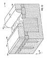
- FIG. 3illustrates the substrate 110 of FIG. 2 after formation of outer side-wall spacers 124 .
- the outer side-wall spacers 124may be formed by depositing a conformal nitride film (or other appropriate material) by method know in the art, e.g., chemical-vapor deposition, and etching the nitride film with an anisotropic etch, such as a plama etch.
- the spacers 124may have a thickness 126 that is generally equal to or less than 0.35 F, 0.25 F, or 0.15 F, or some other distance, depending on the application.
- the outer side-wall spacers 124may be made from a different material than the mask 116 to facilitate selective removal of the mask 116 in a subsequent step.
- the substrate 110may be etched, using the structures 124 and 116 as a hard mask, to form deep trenches 128 , as illustrated by FIG. 4 .
- the deep trenches 128may be generally complementary to the outer profile of the outer side-wall spacers 124 , and the trenches 128 may extend generally perpendicularly into the substrate 110 relative to the surface of the substrate 110 .
- the deep trenches 128may be filled with a sacrificial material 130 , as illustrated by FIG. 5 .
- the sacrificial material 130may be an oxide, spun on glass (SOG), or other appropriate material that has been deposited and planarized with, for example, chemical mechanical planarization (CMP), or an isotropic etch to remove an overburden.
- CMPchemical mechanical planarization
- the mask 116may be removed, as illustrated by FIG. 6 .
- the mask 116may be etched with a process that is selective to both the outer side-wall spacers 124 and the sacrificial material 130 , so that at least a portion or substantially all of these structures 124 and 130 remain on the substrate 110 .
- the voids 132 left by removing the mask 116are generally identical to the shape of the mask 116 .
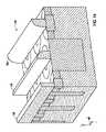
- an inner side-wall spacer 133is formed in the void 132 , as illustrated by FIG. 7 .
- the inner side-wall spacer 133may have a width 134 that is generally equal to or less than 0.35 F, 0.25 F, or 0.15 F, or some other distance, depending on the application.
- the inner side-wall spacer 133is formed by depositing a blanket film, such as a nitride film, and isotropically etching the blanket film to leave the inner side-wall spacer 133 along the walls of the void 132 .
- the inner side-wall spacer 133may be the same material and have the same width 134 as the outer side-wall spacer 124 , or it may be a different material or have a different width.
- the substrate 110may be etched, using the inner side-wall spacer 133 as a hard mask, as illustrated by FIG. 8 .
- This etchmay form shallow trenches 136 (which are shallow in the sense that they are not as deep as the deep trenches described above) in the interior of the space defined by the inner side-wall spacer 133 .
- the depth of the shallow trench 136may be greater than the depth of the upper doped layer 112 .
- the shallow trench 136may be etched with an anisotropic plasma etch or other appropriate process.
- the sacrificial material 130 , the inner side-wall spacer 133 , and the outer-the side-wall spacer 124may be removed, as illustrated by FIG. 9 .
- These features 124 , 130 , and 133may be removed with a wet etch or other process that is selective to the material that makes up the substrate 110 .
- the deep trench 128 and the shallow trench 136combine to define a plurality of precursor pillars 138 .
- Both the position and the shape of the precursor pillars 138may correspond to the position and the shape of the mask 116 ( FIG. 1 ).
- the precursor pillars 138may each define a generally right-elliptical cylinder that extends generally perpendicularly from the surface of the substrate 110 .
- the precursor pillars 138are not exactly elliptical because the side-wall spacers 124 and 133 added a generally uniform distance around and within the perimeter of the generally elliptical mask 116 .
- the precursor pillars 138may include a generally elliptical tube 140 disposed on top of a generally elliptical cylinder 142 .
- the distance 144 between the inner side-wall of the tubes 140 and the outer sidewall of the tubes 140may be approximately equal to or less than 0.7 F, 0.5 F, or 0.3 F, or some other distance.
- the shape of the interior of the tubes 140may be characterized by an inner major axis 146 and an inner minor axis 148 , and the shape of the pillars 138 may be characterized by an outer major axis 150 and an outer minor axis 152 .
- the distance 153 between precursor pillars 138 in adjacent rowsmay be approximately equal to or less than 0.7 F, 0.5 F, or 0.3 F, or some other distance, depending on the application.
- FIG. 10is a top view of the substrate 110 .
- FIG. 10includes dotted lines that illustrate one way in which the precursor pillars 138 may be aligned.
- the precursor pillars 138are positioned such that adjacent sub-columns 154 and 156 overlap one another.
- the sub-columns 154 and 156may combine to form a single column of finFETs on alternating sides of a conductor, such as a data line.
- inner side-wall 158is generally aligned with outer sidewall 160 , but in other embodiments, the tube portions 140 of the pillars 138 may only partially overlap or may not overlap at all.
- These overlapping portions of the precursor pillars 138after subsequent processing, in some embodiments, facilitate generally direct connections from generally straight digit lines to transistors, as explained below.
- a field dielectric 162may be formed, as illustrated by FIG. 11 .
- the field dielectric 162may be an oxide that is deposited with chemical-vapor deposition or a high density plasma process, or in other embodiments, the field dielectric 162 may be grown by reacting the substrate 110 with oxygen in a furnace or with other techniques known in the art. Some embodiments may retain a portion of the sacrificial material 130 as the field dielectric 162 .
- the field dielectric 162may substantially or entirely fill both the deep trenches 128 and the shallow trenches 136 .
- the substrate 110may be patterned with rows and selectively etched with an intermediate trench etch, as illustrated by FIGS. 12-17 .
- FIGS. 12-14illustrate a process for patterning the rows before an intermediate trench etch
- FIGS. 15-17illustrate the resulting structures.
- a mask 164may be formed on the substrate 110 .
- the mask 164may be a hard mask, such as a carbon hard mask or a mask formed by selectively etching lines in a blanket oxide or nitride film, or some other material.
- the mask 164may include an open region 167 and an obstructed region 166 , and the mask 164 may repeat over a period 165 .
- the size of the period 165may be generally equal to the period 121 of the mask 116 , and the size of the obstructed region 166 may be generally equal to one half the period 165 minus the width 169 of a side-wall spacer 168 formed in the next step and illustrated by FIG. 13 .
- the mask 164may be removed with an etch that is selective to the side-wall spacer 168 , thereby leaving the side-wall spacer 168 and exposing the portion of the substrate 110 under the mask 164 , as illustrated by FIG. 14 .
- the substrate 110may be etched with an anisotropic etch to form rows 170 , and the side-wall spacers 166 may be removed, as illustrated by FIG. 16 .
- the mask 164is not double-pitched, and the pattern from the mask 164 is used to form rows 170 directly.
- the mask 164may be formed, and in some embodiments, its line width adjusted with an etchback, reflow, or other thinning process.
- FIGS. 16-18illustrate various aspects of the rows 170 .
- the rows 170 in this embodimentare generally straight, generally parallel to the minor axes 120 of the ellipses of the mask 116 ( FIG. 2 ), and generally centered over the central axis 122 of the mask 116 ( FIG. 2 ).
- the alignment margin for the rows 170may be increased by the elliptical shape of the mask 164 . Because the mask 116 has a generally elliptical shape, the alignment and dimensional tolerances for the mask 164 may be increased in the direction of the major axis 118 ( FIG. 2 ) relative to a mask 116 that has circles.
- the rows 170may be shifted some distance so that they are not necessarily centered on the central axis 122 of the ellipses. In this embodiment, though, the rows 170 are positioned and sized to generally fall entirely or substantially within the space defined by the generally elliptical shallow trench 136 ( FIG. 8 ).
- the rows 170have a width 172 that may generally correspond to the width 169 of the side-wall spacers 168 .
- the width 172is generally uniform along the length and height of the illustrated rows 170 , but in other embodiments, the rows 170 may taper wider toward their base or have some other shape. Further, in some embodiments, the rows 170 may not be generally straight, e.g., the rows 170 may undulate according to the mask 116 .
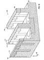
- FIG. 17illustrates the substrate 100 without the field dielectric 162 .
- the substrate 110includes a plurality of pillars 174 that are formed by removing material from the precursor pillars 138 ( FIG. 9 ).
- each of the pillars 174includes a base 176 that is a generally right-elliptical cylinder extending generally perpendicularly from the substrate 110 .
- Extending from the bases 176are fins 178 , each having a gap 180 (e.g., a U-shaped gap) that defines two legs 182 .
- the fins 178each may have two generally planar walls 184 and 186 and two generally convex-curved side-walls 188 and 190 . Additionally, the sides of the gaps 180 include two generally concave-curved side-walls 192 and 194 . The curvature of these walls 184 , 186 , 192 , and 194 is illustrated in the top view of FIG. 18 . As illustrated by FIG. 17 , in this embodiment, the distal portion of the legs 182 are differently doped from the other portions of the pillars 174 . As mentioned above with reference to FIG. 1 , the substrate 110 includes upper doped layer 112 and lower doped layer 114 . In this embodiment, the upper doped layer 112 does not extend below the depth of the gaps 180 .
- gates 198are formed, as illustrated by FIG. 20 .
- the gatesmay be made of metal, doped polysilicon, TiN, or other appropriate conductive materials.
- the gates 198are formed by depositing a blanket film of the gate material and anisotropically etching the gate material to leave side-wall spacers of gate material.
- the illustrated gates 198extend along the sides of the rows 170 so that they overlap both the bottom of the gaps 180 and the upper doped layer 112 of the substrate 110 that form the distal portion of the legs 182 .
- the gates 198may have a width 195 that is generally equal to or less than 0.5 F, and they may be separated by a gap that is generally equal to 0.5 F.
- the transistors 199may connect to other transistors 199 to form a processor, an application specific integrated circuit (ASIC), or static random access memory (SRAM), or the transistors may connect to a device specifically configured to store data, such as a capacitor or phase change memory.
- ASICapplication specific integrated circuit
- SRAMstatic random access memory
- FIGS. 21-23One example of a process that forms a memory device is illustrated by FIGS. 21-23 .
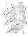
- the transistors 199extend out under alternating sides of the data lines 202 , as illustrated by FIG. 22 .
- the transistor 199 ′′is on a different side of the data line 202 from the transistors 199 ′ and 199 ′′′, which are adjacent the transistor 199 ′′ in the direction of the data lines 202 .
- the transistors 199 ′, 199 ′′, and 199 ′′′are part of a column 201 ′′, which is partially overlapped by adjacent columns 201 ′ and 201 ′′′.
- the columns 201may not overlap, and the transistors 199 may be on the same side of the data lines 202 .
- the other terminal of the transistors 199may be connected to capacitor plates 204 , as illustrated by FIG. 23 .
- the capacitor plates 204may each include a neck 206 and a cup 208 .
- the necks 206may connect the capacitors 204 to the source or drain of the transistors 199 via an exposed, top portion of one of the legs 182 .
- the capacitor plates 204may be coated with both a dielectric and another conductive film. The second film may form another plate to create capacitors connected to the transistors 199 .
- each pair of a capacitor plate 204 and transistor 199may cooperate to store data by accumulating a charge on the capacitor plates 204 .
- the associated transistor 199may be turned on by energizing its gate(s) 198 ( FIG. 20 ), and current 200 may flow through the transistor 199 to or from the capacitor plate 204 .
- the capacitor plates 204may be addressed according to the combination of the gate(s) 198 and the data line 200 that connect to the transistor 199 associated with a given capacitor plate 204 .
- the gates 198may be referred to as word lines, and the data lines 200 may be referred to as bit lines.
- the associated transistor 199may be turned on, and the voltage of the data line 200 connected to the transistor 199 may be sensed.
Landscapes
- Engineering & Computer Science (AREA)
- Manufacturing & Machinery (AREA)
- Semiconductor Memories (AREA)
- Thin Film Transistor (AREA)
Abstract
Description
Claims (13)
Priority Applications (8)
| Application Number | Priority Date | Filing Date | Title |
|---|---|---|---|
| US12/052,537US7808042B2 (en) | 2008-03-20 | 2008-03-20 | Systems and devices including multi-gate transistors and methods of using, making, and operating the same |
| CN200980109446.5ACN101978482B (en) | 2008-03-20 | 2009-03-11 | Systems and devices including multi-gate transistors and methods of using, making, and operating the same |
| PCT/US2009/036816WO2009117295A1 (en) | 2008-03-20 | 2009-03-11 | Systems and devices including multi-gate transistors and methods of using, making, and operating the same |
| KR1020107023371AKR101538821B1 (en) | 2008-03-20 | 2009-03-11 | Systems and devices including multi-gate transistors and methods of using, making, and operating the same |
| TW098108987ATWI447907B (en) | 2008-03-20 | 2009-03-19 | System and device including multi-gate transistor and use, manufacturing and operation method thereof |
| US12/871,700US7981736B2 (en) | 2008-03-20 | 2010-08-30 | Systems and devices including multi-gate transistors and methods of using, making, and operating the same |
| US13/183,337US8450785B2 (en) | 2008-03-20 | 2011-07-14 | Systems and devices including multi-gate transistors and methods of using, making, and operating the same |
| US13/891,538US8759889B2 (en) | 2008-03-20 | 2013-05-10 | Systems and devices including multi-gate transistors and methods of using, making, and operating the same |
Applications Claiming Priority (1)
| Application Number | Priority Date | Filing Date | Title |
|---|---|---|---|
| US12/052,537US7808042B2 (en) | 2008-03-20 | 2008-03-20 | Systems and devices including multi-gate transistors and methods of using, making, and operating the same |
Related Child Applications (1)
| Application Number | Title | Priority Date | Filing Date |
|---|---|---|---|
| US12/871,700DivisionUS7981736B2 (en) | 2008-03-20 | 2010-08-30 | Systems and devices including multi-gate transistors and methods of using, making, and operating the same |
Publications (2)
| Publication Number | Publication Date |
|---|---|
| US20090238000A1 US20090238000A1 (en) | 2009-09-24 |
| US7808042B2true US7808042B2 (en) | 2010-10-05 |
Family
ID=40671452
Family Applications (4)
| Application Number | Title | Priority Date | Filing Date |
|---|---|---|---|
| US12/052,537ActiveUS7808042B2 (en) | 2008-03-20 | 2008-03-20 | Systems and devices including multi-gate transistors and methods of using, making, and operating the same |
| US12/871,700ActiveUS7981736B2 (en) | 2008-03-20 | 2010-08-30 | Systems and devices including multi-gate transistors and methods of using, making, and operating the same |
| US13/183,337Active2028-05-19US8450785B2 (en) | 2008-03-20 | 2011-07-14 | Systems and devices including multi-gate transistors and methods of using, making, and operating the same |
| US13/891,538ActiveUS8759889B2 (en) | 2008-03-20 | 2013-05-10 | Systems and devices including multi-gate transistors and methods of using, making, and operating the same |
Family Applications After (3)
| Application Number | Title | Priority Date | Filing Date |
|---|---|---|---|
| US12/871,700ActiveUS7981736B2 (en) | 2008-03-20 | 2010-08-30 | Systems and devices including multi-gate transistors and methods of using, making, and operating the same |
| US13/183,337Active2028-05-19US8450785B2 (en) | 2008-03-20 | 2011-07-14 | Systems and devices including multi-gate transistors and methods of using, making, and operating the same |
| US13/891,538ActiveUS8759889B2 (en) | 2008-03-20 | 2013-05-10 | Systems and devices including multi-gate transistors and methods of using, making, and operating the same |
Country Status (5)
| Country | Link |
|---|---|
| US (4) | US7808042B2 (en) |
| KR (1) | KR101538821B1 (en) |
| CN (1) | CN101978482B (en) |
| TW (1) | TWI447907B (en) |
| WO (1) | WO2009117295A1 (en) |
Cited By (12)
| Publication number | Priority date | Publication date | Assignee | Title |
|---|---|---|---|---|
| US20090251946A1 (en)* | 2008-04-03 | 2009-10-08 | Micron Technology, Inc. | Data cells with drivers and methods of making and operating the same |
| US8149619B2 (en) | 2008-03-20 | 2012-04-03 | Micron Technology, Inc. | Memory structure having volatile and non-volatile memory portions |
| US8294511B2 (en) | 2010-11-19 | 2012-10-23 | Micron Technology, Inc. | Vertically stacked fin transistors and methods of fabricating and operating the same |
| US8293602B2 (en) | 2010-11-19 | 2012-10-23 | Micron Technology, Inc. | Method of fabricating a finFET having cross-hair cells |
| US8921899B2 (en) | 2010-11-19 | 2014-12-30 | Micron Technology, Inc. | Double gated 4F2 dram CHC cell and methods of fabricating the same |
| US20150140796A1 (en)* | 2013-11-15 | 2015-05-21 | Taiwan Semiconductor Manufacturing Co., Ltd. | Formation of contact/via hole with self-alignment |
| US9331203B2 (en) | 2008-03-06 | 2016-05-03 | Micron Technology, Inc. | Devices with cavity-defined gates and methods of making the same |
| US9449652B2 (en) | 2008-03-20 | 2016-09-20 | Micron Technology, Inc. | Systems and devices including multi-transistor cells and methods of using, making, and operating the same |
| US20160322363A1 (en)* | 2009-11-04 | 2016-11-03 | Micron Technology, Inc. | Memory cells having a folded digit line architecture |
| US9553193B2 (en) | 2010-11-19 | 2017-01-24 | Micron Technology, Inc. | Double gated fin transistors and methods of fabricating and operating the same |
| US9721960B2 (en)* | 2015-03-13 | 2017-08-01 | Micron Technology, Inc. | Data line arrangement and pillar arrangement in apparatuses |
| US20240096627A1 (en)* | 2017-01-11 | 2024-03-21 | Tessera Llc | Self aligned pattern formation post spacer etchback in tight pitch configurations |
Families Citing this family (29)
| Publication number | Priority date | Publication date | Assignee | Title |
|---|---|---|---|---|
| JP5107138B2 (en)* | 2008-05-29 | 2012-12-26 | 住友電工デバイス・イノベーション株式会社 | Semiconductor device |
| KR101045090B1 (en)* | 2008-11-13 | 2011-06-29 | 주식회사 하이닉스반도체 | Method of forming fine pattern of semiconductor device |
| US9202921B2 (en)* | 2010-03-30 | 2015-12-01 | Nanya Technology Corp. | Semiconductor device and method of making the same |
| KR101867503B1 (en)* | 2010-11-19 | 2018-06-15 | 에스케이하이닉스 주식회사 | Method of forming fine pattern for semiconductor device |
| CN102810631B (en)* | 2011-05-31 | 2014-09-24 | 中芯国际集成电路制造(上海)有限公司 | Manufacturing method of phase change memory |
| CN102842580B (en)* | 2011-06-21 | 2015-03-11 | 华邦电子股份有限公司 | Dynamic random access memory and manufacturing method thereof |
| US8697522B2 (en)* | 2011-07-05 | 2014-04-15 | International Business Machines Corporation | Bulk finFET with uniform height and bottom isolation |
| US8437184B1 (en)* | 2011-12-06 | 2013-05-07 | Rexchip Electronics Corporation | Method of controlling a vertical dual-gate dynamic random access memory |
| US9385131B2 (en) | 2012-05-31 | 2016-07-05 | Globalfoundries Inc. | Wrap-around fin for contacting a capacitor strap of a DRAM |
| US8912065B2 (en)* | 2012-06-15 | 2014-12-16 | Nanya Technology Corporation | Method of fabricating semiconductor device |
| US8580634B1 (en)* | 2012-09-11 | 2013-11-12 | Globalfoundries Inc. | Methods of forming 3-D semiconductor devices with a nanowire gate structure wherein the nanowire gate structure is formed prior to source/drain formation |
| US8541274B1 (en)* | 2012-09-11 | 2013-09-24 | Globalfoundries Inc. | Methods of forming 3-D semiconductor devices with a nanowire gate structure wherein the nanowire gate structure is formed after source/drain formation |
| US8889558B2 (en) | 2012-12-12 | 2014-11-18 | Micron Technology, Inc. | Methods of forming a pattern on a substrate |
| US8999852B2 (en)* | 2012-12-12 | 2015-04-07 | Micron Technology, Inc. | Substrate mask patterns, methods of forming a structure on a substrate, methods of forming a square lattice pattern from an oblique lattice pattern, and methods of forming a pattern on a substrate |
| US8889559B2 (en) | 2012-12-12 | 2014-11-18 | Micron Technology, Inc. | Methods of forming a pattern on a substrate |
| US8937018B2 (en) | 2013-03-06 | 2015-01-20 | Micron Technology, Inc. | Methods of forming a pattern on a substrate |
| US8853019B1 (en) | 2013-03-13 | 2014-10-07 | Globalfoundries Inc. | Methods of forming a semiconductor device with a nanowire channel structure by performing an anneal process |
| US8987800B2 (en)* | 2013-03-14 | 2015-03-24 | International Business Machines Corporation | Semiconductor structures with deep trench capacitor and methods of manufacture |
| CN104124210B (en)* | 2013-04-28 | 2016-12-28 | 中芯国际集成电路制造(上海)有限公司 | The forming method of semiconductor structure |
| US9136106B2 (en)* | 2013-12-19 | 2015-09-15 | Taiwan Semiconductor Manufacturing Company, Ltd. | Method for integrated circuit patterning |
| US9431512B2 (en) | 2014-06-18 | 2016-08-30 | Globalfoundries Inc. | Methods of forming nanowire devices with spacers and the resulting devices |
| US9490340B2 (en) | 2014-06-18 | 2016-11-08 | Globalfoundries Inc. | Methods of forming nanowire devices with doped extension regions and the resulting devices |
| US9698025B2 (en)* | 2014-09-04 | 2017-07-04 | Globalfoundries Inc. | Directed self-assembly material growth mask for forming vertical nanowires |
| US9908975B2 (en)* | 2014-09-29 | 2018-03-06 | Guill Tool & Engineering, Co., Inc | Microlayer coextrusion for compounding, pelletizing, and masterbatches |
| US9543304B2 (en)* | 2015-04-02 | 2017-01-10 | Stmicroelectronics, Inc. | Vertical junction FinFET device and method for manufacture |
| CN204889142U (en)* | 2015-09-01 | 2015-12-23 | 浙江永强集团股份有限公司 | Solar energy multi function table |
| US10014302B1 (en)* | 2016-12-27 | 2018-07-03 | Micron Technology, Inc. | Methods of forming memory arrays |
| US10756217B2 (en)* | 2018-02-15 | 2020-08-25 | Micron Technology, Inc. | Access devices formed with conductive contacts |
| JP7059091B2 (en) | 2018-04-24 | 2022-04-25 | モレックス エルエルシー | Electronic components |
Citations (92)
| Publication number | Priority date | Publication date | Assignee | Title |
|---|---|---|---|---|
| US3885861A (en) | 1972-10-02 | 1975-05-27 | Hughes Aircraft Co | Liquid crystal digital reticle |
| US5160987A (en) | 1989-10-26 | 1992-11-03 | International Business Machines Corporation | Three-dimensional semiconductor structures formed from planar layers |
| US5196910A (en) | 1987-04-24 | 1993-03-23 | Hitachi, Ltd. | Semiconductor memory device with recessed array region |
| KR930005234B1 (en) | 1990-09-13 | 1993-06-16 | 금성일렉트론주식회사 | Cell manufacture method of fin-stack cell |
| WO1997028532A1 (en) | 1996-02-01 | 1997-08-07 | Micron Technology, Inc. | Digit line architecture for dynamic memory |
| US5661061A (en) | 1994-03-25 | 1997-08-26 | Hitachi, Ltd. | Process for fabricating a semiconductor integrated circuit device having the multi-layered fin structure |
| US5821513A (en) | 1996-06-26 | 1998-10-13 | Telxon Corporation | Shopping cart mounted portable data collection device with tethered dataform reader |
| US5858829A (en) | 1998-06-29 | 1999-01-12 | Vanguard International Semiconductor Corporation | Method for fabricating dynamic random access memory (DRAM) cells with minimum active cell areas using sidewall-spacer bit lines |
| US5925918A (en) | 1997-07-30 | 1999-07-20 | Micron, Technology, Inc. | Gate stack with improved sidewall integrity |
| US5949057A (en) | 1996-03-29 | 1999-09-07 | Telxon Corporation | Portable data collection device with crosshair targeting illumination assembly |
| TW380316B (en) | 1998-10-15 | 2000-01-21 | Worldwide Semiconductor Mfg | Manufacturing method for fin-trench-structure capacitor of DRAM |
| US6043562A (en) | 1996-01-26 | 2000-03-28 | Micron Technology, Inc. | Digit line architecture for dynamic memory |
| TW388125B (en) | 1998-08-19 | 2000-04-21 | Vanguard Int Semiconduct Corp | Method for fabricating dynamic random access memory (DRAM) cells with minimum active cell areas |
| US6081008A (en) | 1996-02-14 | 2000-06-27 | Lsi Logic Corporation | Composite trench-fin capacitors for DRAM |
| US6100129A (en) | 1998-11-09 | 2000-08-08 | Worldwide Semiconductor Manufacturing Corporation | Method for making fin-trench structured DRAM capacitor |
| US6130551A (en) | 1998-01-19 | 2000-10-10 | Vantis Corporation | Synthesis-friendly FPGA architecture with variable length and variable timing interconnect |
| DE19946719A1 (en) | 1999-09-29 | 2001-04-19 | Infineon Technologies Ag | Trench capacitor used in the production of DRAM storage cells has a conducting contact layer between the substrate and the conducting trench filling in the trench above the insulating collar |
| US20010003034A1 (en) | 1999-02-22 | 2001-06-07 | Toshiharu Furukawa | Fabrication of a high density long channel dram gate with or without a grooved gate |
| US6258656B1 (en) | 1998-09-17 | 2001-07-10 | Siemens Aktiengesellschaft | Capacitor with high-ε dielectric or ferroelectric material based on the fin stack principle and production process using a negative mold |
| US6258659B1 (en) | 2000-11-29 | 2001-07-10 | International Business Machines Corporation | Embedded vertical DRAM cells and dual workfunction logic gates |
| US6268243B1 (en) | 1999-04-15 | 2001-07-31 | Hyundai Electronics Industries Co., Ltd. | Method for fabricating dynamic random access memory cells |
| WO2001061738A1 (en) | 2000-02-15 | 2001-08-23 | Steag Cvd Systems Ltd. | Dram capacitor with ultra-thin nitride layer |
| US6282113B1 (en) | 1999-09-29 | 2001-08-28 | International Business Machines Corporation | Four F-squared gapless dual layer bitline DRAM array architecture |
| US6316309B1 (en) | 1998-06-09 | 2001-11-13 | Steven John Holmes | Method of forming self-isolated and self-aligned 4F-square vertical FET-trench DRAM cells |
| KR20020018071A (en) | 2000-08-28 | 2002-03-07 | 포만 제프리 엘 | Compact dual-port dram architecture system and method for making same |
| WO2002031878A2 (en) | 2000-09-27 | 2002-04-18 | Infineon Technologies North America Corp. | Trench capacitor dram process with protected top oxide during sti etch |
| US6380759B1 (en) | 1997-10-09 | 2002-04-30 | Vantis Corporation | Variable grain architecture for FPGA integrated circuits |
| WO2002049100A2 (en) | 2000-12-14 | 2002-06-20 | Infineon Technologies North America Corp. | Method of forming vertical transistor gate for trench capacitor dram cell |
| US6432769B1 (en) | 1995-10-27 | 2002-08-13 | Hitachi, Ltd. | Semiconductor integrated circuit device and process for manufacture the same |
| US6440792B1 (en) | 1999-11-05 | 2002-08-27 | Promos Technology, Inc. | DRAM technology of storage node formation and no conduction/isolation process of bottle-shaped deep trench |
| US20020155656A1 (en) | 2000-07-14 | 2002-10-24 | Katsuya Hayano | Manufacturing method of semiconductor integrated circuit device, and semiconductor integrated circuit device |
| US20030168676A1 (en) | 1996-07-10 | 2003-09-11 | Fujitsu Limited | Semiconductor device with self-aligned contact and its manufacture |
| US20030198073A1 (en) | 1993-09-15 | 2003-10-23 | Brent Keeth | Bi-level digit line architecture for high density DRAMS |
| US6689660B1 (en) | 1997-07-08 | 2004-02-10 | Micron Technology, Inc. | 4 F2 folded bit line DRAM cell structure having buried bit and word lines |
| US20040027848A1 (en) | 2002-08-12 | 2004-02-12 | Micron Technology, Inc. | 6F2 architecture ROM embedded dram |
| US20040043592A1 (en) | 2002-08-28 | 2004-03-04 | Infineon Technologies Richmond, Lp | Method of forming a gate contact in a semiconductor device |
| WO2004038770A2 (en) | 2002-10-18 | 2004-05-06 | Infineon Technologies Ag | Integrated circuit arrangement comprising a capacitor, and production method |
| US20040125636A1 (en) | 2001-03-14 | 2004-07-01 | Wlodek Kurjanowicz | Interleaved wordline architecture |
| US20040195610A1 (en) | 2003-03-17 | 2004-10-07 | Mutsuo Morikado | Fin semiconductor device and method for fabricating the same |
| US20040202027A1 (en) | 2003-01-21 | 2004-10-14 | Maksim Kuzmenka | Buffer amplifier architecture for semiconductor memory circuits |
| US6845033B2 (en) | 2003-03-05 | 2005-01-18 | International Business Machines Corporation | Structure and system-on-chip integration of a two-transistor and two-capacitor memory cell for trench technology |
| US6897107B2 (en) | 2001-04-11 | 2005-05-24 | International Business Machines Corporation | Method for forming TTO nitride liner for improved collar protection and TTO reliability |
| US20050133852A1 (en) | 1996-05-24 | 2005-06-23 | Jeng-Jye Shau | High performance embedded semiconductor memory devices with multiple dimension first-level bit-lines |
| US20050151206A1 (en) | 2003-12-30 | 2005-07-14 | Schwerin Ulrike G. | Transistor structure with a curved channel, memory cell and memory cell array for DRAMs, and methods for fabricating a DRAM |
| US20050196918A1 (en) | 2004-02-10 | 2005-09-08 | Schwerin Ulrike G. | DRAM memory and method for fabricating a DRAM memory cell |
| US20050245024A1 (en)* | 2004-04-29 | 2005-11-03 | Von Schwerin Ulrike G | Method for production of trench DRAM cells and a trench DRAM cell array with fin field-effect transistors with a curved channel (CFET - curved fets) |
| US6967147B1 (en) | 2000-11-16 | 2005-11-22 | Infineon Technologies Ag | Nitrogen implantation using a shadow effect to control gate oxide thickness in DRAM semiconductor |
| US20060006446A1 (en) | 2004-06-29 | 2006-01-12 | Schwerin Ulrike G | Method for fabricating a DRAM memory cell arrangement having fin field effect transistors and DRAM memory cell |
| US6998666B2 (en) | 2004-01-09 | 2006-02-14 | International Business Machines Corporation | Nitrided STI liner oxide for reduced corner device impact on vertical device performance |
| JP2006054431A (en) | 2004-06-29 | 2006-02-23 | Infineon Technologies Ag | Transistor, memory cell array, and transistor manufacturing method |
| US20060043617A1 (en) | 2004-08-30 | 2006-03-02 | Abbott Todd R | DRAM layout with vertical FETs and method of formation |
| US20060057814A1 (en) | 2004-09-10 | 2006-03-16 | Rolf Weis | Fabricating a memory cell arrangement |
| US20060073662A1 (en) | 2004-10-02 | 2006-04-06 | Se-Myeong Jang | Method of manufacturing multi-channel transistor device and multi-channel transistor device manufactured using the method |
| US20060076602A1 (en) | 2004-09-10 | 2006-04-13 | Johann Harter | Dram cell pair and dram memory cell array |
| US20060131651A1 (en) | 1999-08-31 | 2006-06-22 | Kabushiki Kaisha Toshiba | Semiconductor substrate and its fabrication method |
| US7091543B2 (en) | 2003-05-15 | 2006-08-15 | Taiwan Semiconductor Manufacturing Co., Ltd. | Embedded dual-port DRAM process |
| US7098105B2 (en) | 2004-05-26 | 2006-08-29 | Micron Technology, Inc. | Methods for forming semiconductor structures |
| US7099216B2 (en) | 2003-09-05 | 2006-08-29 | International Business Machines Corporation | Single cycle read/write/writeback pipeline, full-wordline I/O DRAM architecture with enhanced write and single ended sensing |
| US20060246607A1 (en) | 1993-04-02 | 2006-11-02 | Micron Technology, Inc. | Method for forming a storage cell capacitor compatible with high dielectric constant materials |
| US7132333B2 (en) | 2004-09-10 | 2006-11-07 | Infineon Technologies Ag | Transistor, memory cell array and method of manufacturing a transistor |
| US20060270151A1 (en) | 2005-05-31 | 2006-11-30 | Nanya Technology Corporation | Method for forming a semiconductor device |
| US20060273415A1 (en) | 2005-06-01 | 2006-12-07 | Hyun Jung Kim | Transistor for memory device and method for manufacturing the same |
| US20060281250A1 (en) | 2004-12-15 | 2006-12-14 | Till Schloesser | 6F2 access transistor arrangement and semiconductor memory device |
| US7151023B1 (en) | 2005-08-01 | 2006-12-19 | International Business Machines Corporation | Metal gate MOSFET by full semiconductor metal alloy conversion |
| US20070010058A1 (en) | 2005-07-08 | 2007-01-11 | Micron Technology, Inc. | Method and apparatus for a self-aligned recessed access device (RAD) transistor gate |
| US20070023805A1 (en) | 2005-07-26 | 2007-02-01 | Wells David H | Reverse construction memory cell |
| US7190060B1 (en) | 2002-01-09 | 2007-03-13 | Bridge Semiconductor Corporation | Three-dimensional stacked semiconductor package device with bent and flat leads and method of making same |
| US7195995B2 (en) | 2002-08-29 | 2007-03-27 | Micron Technology, Inc. | Method of manufacturing a multilayered doped conductor for a contact in an integrated circuit device |
| US7205241B2 (en)* | 2002-12-10 | 2007-04-17 | Samsung Electronics Co., Ltd. | Method for manufacturing semiconductor device with contact body extended in direction of bit line |
| US7205606B2 (en) | 2003-09-17 | 2007-04-17 | Micron Technology, Inc. | DRAM access transistor |
| US20070096155A1 (en)* | 2005-10-18 | 2007-05-03 | Kyoung-Yun Baek | Cell structure for a semiconductor memory device and method of fabricating the same |
| US20070111455A1 (en) | 2005-11-14 | 2007-05-17 | Samsung Electronics Co., Ltd. | Fabrication of local damascene finFETs using contact type nitride damascene mask |
| US20070121414A1 (en) | 2005-09-12 | 2007-05-31 | Promos Technologies Pte.Ltd. | Shielded bitline architecture for dynamic random access memory (dram) arrays |
| US20070134878A1 (en) | 2005-12-09 | 2007-06-14 | Intel Corporation | Non-planar microelectronic device having isolation element to mitigate fringe effects and method to fabricate same |
| US20070145450A1 (en) | 2005-12-28 | 2007-06-28 | Fei Wang | DRAM cell design with folded digitline sense amplifier |
| US20070166933A1 (en) | 2006-01-16 | 2007-07-19 | Samsung Electronics Co., Ltd. | Methods of Forming Field Effect Transistors and Capacitor-Free Dynamic Random Access Memory Cells |
| US20070170522A1 (en) | 2006-01-23 | 2007-07-26 | Hynix Semiconductor Inc. | Semiconductor device and method for fabricating the same |
| US20070176221A1 (en) | 1995-06-05 | 2007-08-02 | Fujitsu Limited | Semiconductor memory device and method for fabricating the same |
| US20070176222A1 (en) | 1996-07-18 | 2007-08-02 | Fujitsu Limited | Highly integrated and reliable DRAM and its manufacture |
| US20070176253A1 (en) | 2006-01-31 | 2007-08-02 | Peng-Fei Wang | Transistor, memory cell and method of manufacturing a transistor |
| US20070190736A1 (en) | 2006-02-16 | 2007-08-16 | An-Hsiung Liu | Overlay alignment mark and alignment method for the fabrication of trench-capacitor dram devices |
| EP1835530A2 (en) | 2006-03-17 | 2007-09-19 | Samsung Electronics Co., Ltd. | Non-volatile memory device and method of manufacturing the same |
| EP1837906A2 (en) | 2006-03-24 | 2007-09-26 | Samsung Electronics Co., Ltd. | Semiconductor memory device and methods of manufacturing and operating the same |
| US20070258281A1 (en)* | 2006-05-04 | 2007-11-08 | Kenchi Ito | Magnetic memory device |
| US20070262375A1 (en) | 2006-05-12 | 2007-11-15 | Werner Juengling | Non-planar transistor and techniques for fabricating the same |
| WO2008024200A1 (en) | 2006-08-22 | 2008-02-28 | Micron Technology, Inc. | System and method for fabricating a fin field effect transistor |
| US7345937B2 (en) | 2005-03-07 | 2008-03-18 | Micron Technology, Inc | Open digit line array architecture for a memory array |
| US20080253160A1 (en)* | 2007-04-13 | 2008-10-16 | Qimonda Ag | Integrated circuit having a memory cell array and method of forming an integrated circuit |
| US20090238010A1 (en)* | 2008-03-20 | 2009-09-24 | Micron Technology, Inc. | Systems and devices including multi-transistor cells and methods of using, making, and operating the same |
| US20090237996A1 (en)* | 2008-03-20 | 2009-09-24 | Micron Technology, Inc. | Memory structure having volatile and non-volatile memory portions |
| US20090251946A1 (en)* | 2008-04-03 | 2009-10-08 | Micron Technology, Inc. | Data cells with drivers and methods of making and operating the same |
| US20100066440A1 (en)* | 2008-09-15 | 2010-03-18 | Micron Technology, Inc. | Transistor with a passive gate and methods of fabricating the same |
Family Cites Families (5)
| Publication number | Priority date | Publication date | Assignee | Title |
|---|---|---|---|---|
| US5109256A (en) | 1990-08-17 | 1992-04-28 | National Semiconductor Corporation | Schottky barrier diodes and Schottky barrier diode-clamped transistors and method of fabrication |
| KR100577562B1 (en)* | 2004-02-05 | 2006-05-08 | 삼성전자주식회사 | Fin transistor formation method and its structure |
| US7442976B2 (en)* | 2004-09-01 | 2008-10-28 | Micron Technology, Inc. | DRAM cells with vertical transistors |
| EP1764827A1 (en)* | 2005-09-16 | 2007-03-21 | Interuniversitair Microelektronica Centrum ( Imec) | Recursive spacer defined patterning |
| US7928005B2 (en)* | 2005-09-27 | 2011-04-19 | Advanced Micro Devices, Inc. | Method for forming narrow structures in a semiconductor device |
- 2008
- 2008-03-20USUS12/052,537patent/US7808042B2/enactiveActive
- 2009
- 2009-03-11CNCN200980109446.5Apatent/CN101978482B/enactiveActive
- 2009-03-11KRKR1020107023371Apatent/KR101538821B1/enactiveActive
- 2009-03-11WOPCT/US2009/036816patent/WO2009117295A1/enactiveApplication Filing
- 2009-03-19TWTW098108987Apatent/TWI447907B/enactive
- 2010
- 2010-08-30USUS12/871,700patent/US7981736B2/enactiveActive
- 2011
- 2011-07-14USUS13/183,337patent/US8450785B2/enactiveActive
- 2013
- 2013-05-10USUS13/891,538patent/US8759889B2/enactiveActive
Patent Citations (99)
| Publication number | Priority date | Publication date | Assignee | Title |
|---|---|---|---|---|
| US3885861A (en) | 1972-10-02 | 1975-05-27 | Hughes Aircraft Co | Liquid crystal digital reticle |
| US5196910A (en) | 1987-04-24 | 1993-03-23 | Hitachi, Ltd. | Semiconductor memory device with recessed array region |
| US5160987A (en) | 1989-10-26 | 1992-11-03 | International Business Machines Corporation | Three-dimensional semiconductor structures formed from planar layers |
| KR930005234B1 (en) | 1990-09-13 | 1993-06-16 | 금성일렉트론주식회사 | Cell manufacture method of fin-stack cell |
| US20060246607A1 (en) | 1993-04-02 | 2006-11-02 | Micron Technology, Inc. | Method for forming a storage cell capacitor compatible with high dielectric constant materials |
| US20030198073A1 (en) | 1993-09-15 | 2003-10-23 | Brent Keeth | Bi-level digit line architecture for high density DRAMS |
| US5661061A (en) | 1994-03-25 | 1997-08-26 | Hitachi, Ltd. | Process for fabricating a semiconductor integrated circuit device having the multi-layered fin structure |
| US20070176221A1 (en) | 1995-06-05 | 2007-08-02 | Fujitsu Limited | Semiconductor memory device and method for fabricating the same |
| US6432769B1 (en) | 1995-10-27 | 2002-08-13 | Hitachi, Ltd. | Semiconductor integrated circuit device and process for manufacture the same |
| US20040062069A1 (en) | 1996-01-26 | 2004-04-01 | Brent Keeth | Digit line architecture for dynamic memory |
| US6043562A (en) | 1996-01-26 | 2000-03-28 | Micron Technology, Inc. | Digit line architecture for dynamic memory |
| WO1997028532A1 (en) | 1996-02-01 | 1997-08-07 | Micron Technology, Inc. | Digit line architecture for dynamic memory |
| US6081008A (en) | 1996-02-14 | 2000-06-27 | Lsi Logic Corporation | Composite trench-fin capacitors for DRAM |
| US5949057A (en) | 1996-03-29 | 1999-09-07 | Telxon Corporation | Portable data collection device with crosshair targeting illumination assembly |
| US20050133852A1 (en) | 1996-05-24 | 2005-06-23 | Jeng-Jye Shau | High performance embedded semiconductor memory devices with multiple dimension first-level bit-lines |
| US5821513A (en) | 1996-06-26 | 1998-10-13 | Telxon Corporation | Shopping cart mounted portable data collection device with tethered dataform reader |
| US20030168676A1 (en) | 1996-07-10 | 2003-09-11 | Fujitsu Limited | Semiconductor device with self-aligned contact and its manufacture |
| US20070176222A1 (en) | 1996-07-18 | 2007-08-02 | Fujitsu Limited | Highly integrated and reliable DRAM and its manufacture |
| US6689660B1 (en) | 1997-07-08 | 2004-02-10 | Micron Technology, Inc. | 4 F2 folded bit line DRAM cell structure having buried bit and word lines |
| US5925918A (en) | 1997-07-30 | 1999-07-20 | Micron, Technology, Inc. | Gate stack with improved sidewall integrity |
| US6380759B1 (en) | 1997-10-09 | 2002-04-30 | Vantis Corporation | Variable grain architecture for FPGA integrated circuits |
| US6216257B1 (en) | 1997-10-09 | 2001-04-10 | Vantis Corporation | FPGA device and method that includes a variable grain function architecture for implementing configuration logic blocks and a complimentary variable length interconnect architecture for providing configurable routing between configuration logic blocks |
| US6130551A (en) | 1998-01-19 | 2000-10-10 | Vantis Corporation | Synthesis-friendly FPGA architecture with variable length and variable timing interconnect |
| US6316309B1 (en) | 1998-06-09 | 2001-11-13 | Steven John Holmes | Method of forming self-isolated and self-aligned 4F-square vertical FET-trench DRAM cells |
| US5858829A (en) | 1998-06-29 | 1999-01-12 | Vanguard International Semiconductor Corporation | Method for fabricating dynamic random access memory (DRAM) cells with minimum active cell areas using sidewall-spacer bit lines |
| US6008513A (en) | 1998-06-29 | 1999-12-28 | Vanguard International Semiconductor Corporation | Dynamic random access memory (DRAM) cells with minimum active cell areas using sidewall-space bit lines |
| TW388125B (en) | 1998-08-19 | 2000-04-21 | Vanguard Int Semiconduct Corp | Method for fabricating dynamic random access memory (DRAM) cells with minimum active cell areas |
| US6258656B1 (en) | 1998-09-17 | 2001-07-10 | Siemens Aktiengesellschaft | Capacitor with high-ε dielectric or ferroelectric material based on the fin stack principle and production process using a negative mold |
| TW380316B (en) | 1998-10-15 | 2000-01-21 | Worldwide Semiconductor Mfg | Manufacturing method for fin-trench-structure capacitor of DRAM |
| US6100129A (en) | 1998-11-09 | 2000-08-08 | Worldwide Semiconductor Manufacturing Corporation | Method for making fin-trench structured DRAM capacitor |
| US20010003034A1 (en) | 1999-02-22 | 2001-06-07 | Toshiharu Furukawa | Fabrication of a high density long channel dram gate with or without a grooved gate |
| US6268243B1 (en) | 1999-04-15 | 2001-07-31 | Hyundai Electronics Industries Co., Ltd. | Method for fabricating dynamic random access memory cells |
| US20060131651A1 (en) | 1999-08-31 | 2006-06-22 | Kabushiki Kaisha Toshiba | Semiconductor substrate and its fabrication method |
| US6282113B1 (en) | 1999-09-29 | 2001-08-28 | International Business Machines Corporation | Four F-squared gapless dual layer bitline DRAM array architecture |
| DE19946719A1 (en) | 1999-09-29 | 2001-04-19 | Infineon Technologies Ag | Trench capacitor used in the production of DRAM storage cells has a conducting contact layer between the substrate and the conducting trench filling in the trench above the insulating collar |
| US6440792B1 (en) | 1999-11-05 | 2002-08-27 | Promos Technology, Inc. | DRAM technology of storage node formation and no conduction/isolation process of bottle-shaped deep trench |
| WO2001061738A1 (en) | 2000-02-15 | 2001-08-23 | Steag Cvd Systems Ltd. | Dram capacitor with ultra-thin nitride layer |
| US20020155656A1 (en) | 2000-07-14 | 2002-10-24 | Katsuya Hayano | Manufacturing method of semiconductor integrated circuit device, and semiconductor integrated circuit device |
| KR20020018071A (en) | 2000-08-28 | 2002-03-07 | 포만 제프리 엘 | Compact dual-port dram architecture system and method for making same |
| WO2002031878A2 (en) | 2000-09-27 | 2002-04-18 | Infineon Technologies North America Corp. | Trench capacitor dram process with protected top oxide during sti etch |
| US6967147B1 (en) | 2000-11-16 | 2005-11-22 | Infineon Technologies Ag | Nitrogen implantation using a shadow effect to control gate oxide thickness in DRAM semiconductor |
| US6258659B1 (en) | 2000-11-29 | 2001-07-10 | International Business Machines Corporation | Embedded vertical DRAM cells and dual workfunction logic gates |
| WO2002049100A2 (en) | 2000-12-14 | 2002-06-20 | Infineon Technologies North America Corp. | Method of forming vertical transistor gate for trench capacitor dram cell |
| US20040125636A1 (en) | 2001-03-14 | 2004-07-01 | Wlodek Kurjanowicz | Interleaved wordline architecture |
| US6897107B2 (en) | 2001-04-11 | 2005-05-24 | International Business Machines Corporation | Method for forming TTO nitride liner for improved collar protection and TTO reliability |
| US7190060B1 (en) | 2002-01-09 | 2007-03-13 | Bridge Semiconductor Corporation | Three-dimensional stacked semiconductor package device with bent and flat leads and method of making same |
| US20040027848A1 (en) | 2002-08-12 | 2004-02-12 | Micron Technology, Inc. | 6F2 architecture ROM embedded dram |
| US20040043592A1 (en) | 2002-08-28 | 2004-03-04 | Infineon Technologies Richmond, Lp | Method of forming a gate contact in a semiconductor device |
| US6927462B2 (en) | 2002-08-28 | 2005-08-09 | Infineon Technologes Richmond, Lp | Method of forming a gate contact in a semiconductor device |
| US7195995B2 (en) | 2002-08-29 | 2007-03-27 | Micron Technology, Inc. | Method of manufacturing a multilayered doped conductor for a contact in an integrated circuit device |
| WO2004038770A2 (en) | 2002-10-18 | 2004-05-06 | Infineon Technologies Ag | Integrated circuit arrangement comprising a capacitor, and production method |
| US7205241B2 (en)* | 2002-12-10 | 2007-04-17 | Samsung Electronics Co., Ltd. | Method for manufacturing semiconductor device with contact body extended in direction of bit line |
| US20040202027A1 (en) | 2003-01-21 | 2004-10-14 | Maksim Kuzmenka | Buffer amplifier architecture for semiconductor memory circuits |
| US6845033B2 (en) | 2003-03-05 | 2005-01-18 | International Business Machines Corporation | Structure and system-on-chip integration of a two-transistor and two-capacitor memory cell for trench technology |
| US20060244106A1 (en) | 2003-03-17 | 2006-11-02 | Kabushiki Kaisha Toshiba | Fin semiconductor device and method for fabricating the same |
| US20040195610A1 (en) | 2003-03-17 | 2004-10-07 | Mutsuo Morikado | Fin semiconductor device and method for fabricating the same |
| US7091543B2 (en) | 2003-05-15 | 2006-08-15 | Taiwan Semiconductor Manufacturing Co., Ltd. | Embedded dual-port DRAM process |
| US7099216B2 (en) | 2003-09-05 | 2006-08-29 | International Business Machines Corporation | Single cycle read/write/writeback pipeline, full-wordline I/O DRAM architecture with enhanced write and single ended sensing |
| US7205606B2 (en) | 2003-09-17 | 2007-04-17 | Micron Technology, Inc. | DRAM access transistor |
| US20050151206A1 (en) | 2003-12-30 | 2005-07-14 | Schwerin Ulrike G. | Transistor structure with a curved channel, memory cell and memory cell array for DRAMs, and methods for fabricating a DRAM |
| US20070052040A1 (en) | 2003-12-30 | 2007-03-08 | Schwerin Ulrike G | Transistor with contoured channel and method for making the same |
| US6998666B2 (en) | 2004-01-09 | 2006-02-14 | International Business Machines Corporation | Nitrided STI liner oxide for reduced corner device impact on vertical device performance |
| US20050196918A1 (en) | 2004-02-10 | 2005-09-08 | Schwerin Ulrike G. | DRAM memory and method for fabricating a DRAM memory cell |
| US20050245024A1 (en)* | 2004-04-29 | 2005-11-03 | Von Schwerin Ulrike G | Method for production of trench DRAM cells and a trench DRAM cell array with fin field-effect transistors with a curved channel (CFET - curved fets) |
| US7098105B2 (en) | 2004-05-26 | 2006-08-29 | Micron Technology, Inc. | Methods for forming semiconductor structures |
| JP2006054431A (en) | 2004-06-29 | 2006-02-23 | Infineon Technologies Ag | Transistor, memory cell array, and transistor manufacturing method |
| US20060006446A1 (en) | 2004-06-29 | 2006-01-12 | Schwerin Ulrike G | Method for fabricating a DRAM memory cell arrangement having fin field effect transistors and DRAM memory cell |
| US20060043617A1 (en) | 2004-08-30 | 2006-03-02 | Abbott Todd R | DRAM layout with vertical FETs and method of formation |
| US7132333B2 (en) | 2004-09-10 | 2006-11-07 | Infineon Technologies Ag | Transistor, memory cell array and method of manufacturing a transistor |
| US20060076602A1 (en) | 2004-09-10 | 2006-04-13 | Johann Harter | Dram cell pair and dram memory cell array |
| US20060057814A1 (en) | 2004-09-10 | 2006-03-16 | Rolf Weis | Fabricating a memory cell arrangement |
| US20060073662A1 (en) | 2004-10-02 | 2006-04-06 | Se-Myeong Jang | Method of manufacturing multi-channel transistor device and multi-channel transistor device manufactured using the method |
| US20060281250A1 (en) | 2004-12-15 | 2006-12-14 | Till Schloesser | 6F2 access transistor arrangement and semiconductor memory device |
| US7345937B2 (en) | 2005-03-07 | 2008-03-18 | Micron Technology, Inc | Open digit line array architecture for a memory array |
| US20060270151A1 (en) | 2005-05-31 | 2006-11-30 | Nanya Technology Corporation | Method for forming a semiconductor device |
| US20060273415A1 (en) | 2005-06-01 | 2006-12-07 | Hyun Jung Kim | Transistor for memory device and method for manufacturing the same |
| US20070010058A1 (en) | 2005-07-08 | 2007-01-11 | Micron Technology, Inc. | Method and apparatus for a self-aligned recessed access device (RAD) transistor gate |
| US20070023805A1 (en) | 2005-07-26 | 2007-02-01 | Wells David H | Reverse construction memory cell |
| US7151023B1 (en) | 2005-08-01 | 2006-12-19 | International Business Machines Corporation | Metal gate MOSFET by full semiconductor metal alloy conversion |
| US20070121414A1 (en) | 2005-09-12 | 2007-05-31 | Promos Technologies Pte.Ltd. | Shielded bitline architecture for dynamic random access memory (dram) arrays |
| US20070096155A1 (en)* | 2005-10-18 | 2007-05-03 | Kyoung-Yun Baek | Cell structure for a semiconductor memory device and method of fabricating the same |
| US20070111455A1 (en) | 2005-11-14 | 2007-05-17 | Samsung Electronics Co., Ltd. | Fabrication of local damascene finFETs using contact type nitride damascene mask |
| US20070134878A1 (en) | 2005-12-09 | 2007-06-14 | Intel Corporation | Non-planar microelectronic device having isolation element to mitigate fringe effects and method to fabricate same |
| US20070145450A1 (en) | 2005-12-28 | 2007-06-28 | Fei Wang | DRAM cell design with folded digitline sense amplifier |
| US20070166933A1 (en) | 2006-01-16 | 2007-07-19 | Samsung Electronics Co., Ltd. | Methods of Forming Field Effect Transistors and Capacitor-Free Dynamic Random Access Memory Cells |
| US20070170522A1 (en) | 2006-01-23 | 2007-07-26 | Hynix Semiconductor Inc. | Semiconductor device and method for fabricating the same |
| US20070176253A1 (en) | 2006-01-31 | 2007-08-02 | Peng-Fei Wang | Transistor, memory cell and method of manufacturing a transistor |
| US20070190736A1 (en) | 2006-02-16 | 2007-08-16 | An-Hsiung Liu | Overlay alignment mark and alignment method for the fabrication of trench-capacitor dram devices |
| EP1835530A2 (en) | 2006-03-17 | 2007-09-19 | Samsung Electronics Co., Ltd. | Non-volatile memory device and method of manufacturing the same |
| US20070222036A1 (en)* | 2006-03-24 | 2007-09-27 | Samsung Electronics Co., Ltd. | Semiconductor memory device and methods of manufacturing and operating the same |
| EP1837906A2 (en) | 2006-03-24 | 2007-09-26 | Samsung Electronics Co., Ltd. | Semiconductor memory device and methods of manufacturing and operating the same |
| US20070258281A1 (en)* | 2006-05-04 | 2007-11-08 | Kenchi Ito | Magnetic memory device |
| US20070262375A1 (en) | 2006-05-12 | 2007-11-15 | Werner Juengling | Non-planar transistor and techniques for fabricating the same |
| WO2008024200A1 (en) | 2006-08-22 | 2008-02-28 | Micron Technology, Inc. | System and method for fabricating a fin field effect transistor |
| US20080253160A1 (en)* | 2007-04-13 | 2008-10-16 | Qimonda Ag | Integrated circuit having a memory cell array and method of forming an integrated circuit |
| US20090238010A1 (en)* | 2008-03-20 | 2009-09-24 | Micron Technology, Inc. | Systems and devices including multi-transistor cells and methods of using, making, and operating the same |
| US20090237996A1 (en)* | 2008-03-20 | 2009-09-24 | Micron Technology, Inc. | Memory structure having volatile and non-volatile memory portions |
| US20090251946A1 (en)* | 2008-04-03 | 2009-10-08 | Micron Technology, Inc. | Data cells with drivers and methods of making and operating the same |
| US20100066440A1 (en)* | 2008-09-15 | 2010-03-18 | Micron Technology, Inc. | Transistor with a passive gate and methods of fabricating the same |
Non-Patent Citations (25)
| Title |
|---|
| Betty Prince, Ph.D.; "Trends in Scaled and Nanotechnology Memories"; Memory Strategies International; Leander, Texas; 2005. |
| Bor-Wen Chan, Min-Hwa Chi, Liou, Y.H; Notch Elimination in Polycide Gate Stack Etching for Advanced DRAM Technology; Center for Technol. Dev., Worldwide Semicond. Manuf. Corp., Hsinchu; http://ieeexplore.ieee.org/xpl/freeabs-all.jsp?tp=&arnumber=883094&isnumber=19090, 2000. |
| Branislav Curanovic; "Development of a Fully-Depleted Thin-Body FinFET Process"; Department of Microelectronic Engineering, College of Engineering; Rochester Institute of Technology; Rochester, New York; Nov. 2003. |
| Chien Yu, Rich Wise, Anthony Domenicucci; A Two-Step Spacer Etch for High-Aspect-Ration Gate Stack Process; IBM Microelectronics; http://www.mrs.org/s-mrs/s-mrs/sec-subscribe.asp?CID=2353&DID=113693&ation=detail, 2000. |
| Claeys, Cor; "Technological Challenges of Advanced CMOS Processing and Their Impact on Design Aspects"; Proceedings of the 17th International Conference on VLSI Design (VLSID '04); 1063-9667/04; IEEE Computer Society; Leuven, Belgium. |
| Endoh, T., Shinmei, K., Sakuraba, H., Masuoka, F.; New Three-Dimensional Memory Array Architecture for Future Ultrahigh-Density DRAM; Res. Inst. Of Electrical Communication, Tohoku University, Sendai; Solid-State Circuites, IEEE Journal; Apr. 1999; vol. 34, Issue 4, pp. 476-483; hottp://ieeexplore.ieee.org/xpls/abs-all.jsp?arnumber=753680. |
| Enrico Gili; "Fabrication of Vertical MOSFETs With Reduced Parasitics and Suppression of Short Channel Effects"; Department of Electronics and Computer Science, Microelectronics Group; University of Southampton, Jun. 2004 http://66.102.1.104/scholar?hl=en&lr=&q=cache:BErKI49qg2MJ:www.ecs.soton.ac.uk/~eg02r/Public ations/MinithesisEGili.pdf+dram+fins+%22process+flow%22+%22vertical+access%22. |
| Enrico Gili; "Fabrication of Vertical MOSFETs With Reduced Parasitics and Suppression of Short Channel Effects"; Department of Electronics and Computer Science, Microelectronics Group; University of Southampton, Jun. 2004 http://66.102.1.104/scholar?hl=en&lr=&q=cache:BErKI49qg2MJ:www.ecs.soton.ac.uk/˜eg02r/Public ations/MinithesisEGili.pdf+dram+fins+%22process+flow%22+%22vertical+access%22. |
| F. Fishburn, et al.; "A 78nm 6F2 DRAM Technology for Multigigabit Densities", 2004. |
| Ikeda, H., Inukai, H.; High-Speed DRAM Architecture Development; NEC Corp., Sagamihara; Solid-State Circuits, IEEE Journal; May 1999; vol. 34, Issue 5, pp. 685-692; http://ieeexplore.ieee.org/xpls/abs-all.jsp?arnumber=760380&isnumber=16453. |
| J. Sturm, et al.; "Increased Transconductance in Fully-Depleted Ultra-Thin Silicon-on-Insulator MOSFETs"; 6 pages, 1988. |
| J-H. Ahn, S-H. Hong, S-J. Kim, J-B. Ko, S-W. Shin, S-D. Lee, Y-W. Kim, K-S. Lee, S-K. Lee, S-E. Jang, J-H. Choi, S-Y. Kim, G-H. Baw, S-W. Park, Y-J. Park, "An Experimental 256Mb Non-Volatile DRAM with Cell Plate Boosted Programming Technique". IEEE International Solid-State Circuits Conference, ISSCC 2004 / Session 2 / Non-Volatile Memory / 2.2, 2004. |
| Johgn-Man Park, Sang-Yeon Han, Chang-Hoon Jeon, Si-Ok Sohn, Jun-Bum Lee, Yamada, S., Shin-Deuk Kim, Wook-Je Kim; Wouns Yang, Donggun Park, Byung-IL Ryu; Fully Integrated Advanced Bulk FinFETs Architecture Featuring Partially-Insulating Technique for DRAM Cell Application of 40nm Generation and Beyond; http://ieeexplore.ieee.org/xpl/freeabs-all.jsp?arnumber=4154360, Dec. 2006. |
| R. Katsumata, et al.; "Fin-Array-FET on bulk silicon for sub-100 nm Trench Capacitor DRAM"; 2003 Symposium on VLSI Technology Digest of Technical Papers; Jun. 2003, 2 pages. |
| T. Park, et al.; "Fabrication of Body-Tied FinFETs (Oega MOSFETs) Using Bulk Si Wafers"; 2003 Symposium on VLSI Technology Digest of Technical Papers; Jun. 2003, 2 pages. |
| Takashima, D., Nakano, H.; A Cell Transistor Scalable DRAM Array Architecture; Memory LSI Res. & Dev. Center, Toshiba Corporation, Yokohama; Solid-State Circuits, IEEE Journal; May 2002; vol. 37, Issue 5, pp. 587-591; http://ieeexplore.ieee.org/xpls/abs-all.jsp?arnumber=997851. |
| U.S. Appl. No. 12/033,768, filed Feb. 19, 2008, Werner Juengling. |
| U.S. Appl. No. 12/033,780, filed Feb. 19, 2008, Werner Juengling. |
| U.S. Appl. No. 12/033,799, filed Feb. 19, 2008, Werner Juengling. |
| U.S. Appl. No. 12/043,813, filed Mar. 6, 2008, Werner Juengling. |
| U.S. Appl. No. 12/052,300, filed Mar. 20, 2008, Werner Juengling. |
| U.S. Appl. No. 12/052,317, filed Mar. 20, 2008, Werner Juengling. |
| U.S. Appl. No. 12/052,537, filed Mar. 20, 2008, Werner Juengling. |
| U.S. Appl. No. 12/062,354, filed Apr. 3, 2008, Werner Juengling. |
| U.S. Appl. No. 12/130,825, filed May 30, 2008, Werner Juengling. |
Cited By (22)
| Publication number | Priority date | Publication date | Assignee | Title |
|---|---|---|---|---|
| US9331203B2 (en) | 2008-03-06 | 2016-05-03 | Micron Technology, Inc. | Devices with cavity-defined gates and methods of making the same |
| US8149619B2 (en) | 2008-03-20 | 2012-04-03 | Micron Technology, Inc. | Memory structure having volatile and non-volatile memory portions |
| US9449652B2 (en) | 2008-03-20 | 2016-09-20 | Micron Technology, Inc. | Systems and devices including multi-transistor cells and methods of using, making, and operating the same |
| US8750025B2 (en) | 2008-04-03 | 2014-06-10 | Micron Technology, Inc. | Data cells with drivers and methods of making and operating the same |
| US7969776B2 (en) | 2008-04-03 | 2011-06-28 | Micron Technology, Inc. | Data cells with drivers and methods of making and operating the same |
| US20090251946A1 (en)* | 2008-04-03 | 2009-10-08 | Micron Technology, Inc. | Data cells with drivers and methods of making and operating the same |
| US8503228B2 (en) | 2008-04-03 | 2013-08-06 | Micron Technology, Inc. | Data cells with drivers and methods of making and operating the same |
| US8537608B2 (en) | 2008-04-03 | 2013-09-17 | Micron Technology, Inc. | Data cells with drivers and methods of making and operating the same |
| US20160322363A1 (en)* | 2009-11-04 | 2016-11-03 | Micron Technology, Inc. | Memory cells having a folded digit line architecture |
| US9653468B2 (en)* | 2009-11-04 | 2017-05-16 | Micron Technology, Inc. | Memory cells having a folded digit line architecture |
| US8294511B2 (en) | 2010-11-19 | 2012-10-23 | Micron Technology, Inc. | Vertically stacked fin transistors and methods of fabricating and operating the same |
| US8598653B2 (en) | 2010-11-19 | 2013-12-03 | Micron Technology, Inc. | FinFET having cross-hair cells |
| US8293602B2 (en) | 2010-11-19 | 2012-10-23 | Micron Technology, Inc. | Method of fabricating a finFET having cross-hair cells |
| US9472461B2 (en) | 2010-11-19 | 2016-10-18 | Micron Technology, Inc. | Double gated 4F2 dram CHC cell and methods of fabricating the same |
| US8921899B2 (en) | 2010-11-19 | 2014-12-30 | Micron Technology, Inc. | Double gated 4F2 dram CHC cell and methods of fabricating the same |
| US9553193B2 (en) | 2010-11-19 | 2017-01-24 | Micron Technology, Inc. | Double gated fin transistors and methods of fabricating and operating the same |
| US8962401B2 (en) | 2010-11-19 | 2015-02-24 | Micron Technology, Inc. | Double gated 4F2 dram CHC cell and methods of fabricating the same |
| US20150140796A1 (en)* | 2013-11-15 | 2015-05-21 | Taiwan Semiconductor Manufacturing Co., Ltd. | Formation of contact/via hole with self-alignment |
| US9805934B2 (en)* | 2013-11-15 | 2017-10-31 | Taiwan Semiconductor Manufacturing Co., Ltd. | Formation of contact/via hole with self-alignment |
| US9721960B2 (en)* | 2015-03-13 | 2017-08-01 | Micron Technology, Inc. | Data line arrangement and pillar arrangement in apparatuses |
| US20240096627A1 (en)* | 2017-01-11 | 2024-03-21 | Tessera Llc | Self aligned pattern formation post spacer etchback in tight pitch configurations |
| US12106963B2 (en)* | 2017-01-11 | 2024-10-01 | Tessera Llc | Self aligned pattern formation post spacer etchback in tight pitch configurations |
Also Published As
| Publication number | Publication date |
|---|---|
| KR20100139045A (en) | 2010-12-31 |
| KR101538821B1 (en) | 2015-07-23 |
| US20120018789A1 (en) | 2012-01-26 |
| TWI447907B (en) | 2014-08-01 |
| US7981736B2 (en) | 2011-07-19 |
| TW200950079A (en) | 2009-12-01 |
| US20090238000A1 (en) | 2009-09-24 |
| CN101978482A (en) | 2011-02-16 |
| US8759889B2 (en) | 2014-06-24 |
| US8450785B2 (en) | 2013-05-28 |
| US20130240967A1 (en) | 2013-09-19 |
| CN101978482B (en) | 2012-11-14 |
| US20100323481A1 (en) | 2010-12-23 |
| WO2009117295A1 (en) | 2009-09-24 |
Similar Documents
| Publication | Publication Date | Title |
|---|---|---|
| US7808042B2 (en) | Systems and devices including multi-gate transistors and methods of using, making, and operating the same | |
| US9984936B1 (en) | Methods of forming an isolated nano-sheet transistor device and the resulting device | |
| US10103238B1 (en) | Nanosheet field-effect transistor with full dielectric isolation | |
| US9646990B2 (en) | NAND memory strings and methods of fabrication thereof | |
| CN109103193B (en) | Vertical memory device | |
| US8058683B2 (en) | Access device having vertical channel and related semiconductor device and a method of fabricating the access device | |
| US8076190B2 (en) | Sea-of-fins structure on a semiconductor substrate and method of fabrication | |
| US20180182757A1 (en) | Tall single-fin fin-type field effect transistor structures and methods | |
| US10388747B1 (en) | Gate contact structure positioned above an active region with air gaps positioned adjacent the gate structure | |
| KR20110027719A (en) | Method of providing electrical isolation and semiconductor structures comprising electrical isolation | |
| US10475904B2 (en) | Methods of forming merged source/drain regions on integrated circuit products | |
| US11678485B2 (en) | Vertical memory devices | |
| TW201830704A (en) | Integration of vertical field effect transistor and saddle fin field effect transistor | |
| US20200243643A1 (en) | Integrated circuit product with a multi-layer single diffusion break and methods of making such products | |
| US20220310594A1 (en) | Semiconductor device and method of manufacturing semiconductor device | |
| WO2023142521A1 (en) | Memory provided with vertical channel transistor and manufacturing method therefor | |
| US9685540B2 (en) | Semiconductor device having a gate that is buried in an active region and a device isolation film | |
| US20210057288A1 (en) | Semiconductor device and method of fabricating the same | |
| CN115020349A (en) | Semiconductor structure and preparation method thereof | |
| US20200119043A1 (en) | Vertical memory devices | |
| US9607993B1 (en) | Capacitor-transistor strap connections for a memory cell | |
| US20070007600A1 (en) | MOS transistor and method of manufacturing the same | |
| US20250016979A1 (en) | Semiconductor device | |
| CN117276077A (en) | Semiconductor structure manufacturing method and semiconductor structure |
Legal Events
| Date | Code | Title | Description |
|---|---|---|---|
| AS | Assignment | Owner name:MICRON TECHNOLOGY, INC., IDAHO Free format text:ASSIGNMENT OF ASSIGNORS INTEREST;ASSIGNOR:JUENGLING, WERNER;REEL/FRAME:020682/0556 Effective date:20080318 | |
| FEPP | Fee payment procedure | Free format text:PAYOR NUMBER ASSIGNED (ORIGINAL EVENT CODE: ASPN); ENTITY STATUS OF PATENT OWNER: LARGE ENTITY | |
| STCF | Information on status: patent grant | Free format text:PATENTED CASE | |
| FPAY | Fee payment | Year of fee payment:4 | |
| AS | Assignment | Owner name:U.S. BANK NATIONAL ASSOCIATION, AS COLLATERAL AGENT, CALIFORNIA Free format text:SECURITY INTEREST;ASSIGNOR:MICRON TECHNOLOGY, INC.;REEL/FRAME:038669/0001 Effective date:20160426 Owner name:U.S. BANK NATIONAL ASSOCIATION, AS COLLATERAL AGEN Free format text:SECURITY INTEREST;ASSIGNOR:MICRON TECHNOLOGY, INC.;REEL/FRAME:038669/0001 Effective date:20160426 | |
| AS | Assignment | Owner name:MORGAN STANLEY SENIOR FUNDING, INC., AS COLLATERAL AGENT, MARYLAND Free format text:PATENT SECURITY AGREEMENT;ASSIGNOR:MICRON TECHNOLOGY, INC.;REEL/FRAME:038954/0001 Effective date:20160426 Owner name:MORGAN STANLEY SENIOR FUNDING, INC., AS COLLATERAL Free format text:PATENT SECURITY AGREEMENT;ASSIGNOR:MICRON TECHNOLOGY, INC.;REEL/FRAME:038954/0001 Effective date:20160426 | |
| AS | Assignment | Owner name:U.S. BANK NATIONAL ASSOCIATION, AS COLLATERAL AGENT, CALIFORNIA Free format text:CORRECTIVE ASSIGNMENT TO CORRECT THE REPLACE ERRONEOUSLY FILED PATENT #7358718 WITH THE CORRECT PATENT #7358178 PREVIOUSLY RECORDED ON REEL 038669 FRAME 0001. ASSIGNOR(S) HEREBY CONFIRMS THE SECURITY INTEREST;ASSIGNOR:MICRON TECHNOLOGY, INC.;REEL/FRAME:043079/0001 Effective date:20160426 Owner name:U.S. BANK NATIONAL ASSOCIATION, AS COLLATERAL AGEN Free format text:CORRECTIVE ASSIGNMENT TO CORRECT THE REPLACE ERRONEOUSLY FILED PATENT #7358718 WITH THE CORRECT PATENT #7358178 PREVIOUSLY RECORDED ON REEL 038669 FRAME 0001. ASSIGNOR(S) HEREBY CONFIRMS THE SECURITY INTEREST;ASSIGNOR:MICRON TECHNOLOGY, INC.;REEL/FRAME:043079/0001 Effective date:20160426 | |
| MAFP | Maintenance fee payment | Free format text:PAYMENT OF MAINTENANCE FEE, 8TH YEAR, LARGE ENTITY (ORIGINAL EVENT CODE: M1552) Year of fee payment:8 | |
| AS | Assignment | Owner name:JPMORGAN CHASE BANK, N.A., AS COLLATERAL AGENT, ILLINOIS Free format text:SECURITY INTEREST;ASSIGNORS:MICRON TECHNOLOGY, INC.;MICRON SEMICONDUCTOR PRODUCTS, INC.;REEL/FRAME:047540/0001 Effective date:20180703 Owner name:JPMORGAN CHASE BANK, N.A., AS COLLATERAL AGENT, IL Free format text:SECURITY INTEREST;ASSIGNORS:MICRON TECHNOLOGY, INC.;MICRON SEMICONDUCTOR PRODUCTS, INC.;REEL/FRAME:047540/0001 Effective date:20180703 | |
| AS | Assignment | Owner name:MICRON TECHNOLOGY, INC., IDAHO Free format text:RELEASE BY SECURED PARTY;ASSIGNOR:U.S. BANK NATIONAL ASSOCIATION, AS COLLATERAL AGENT;REEL/FRAME:047243/0001 Effective date:20180629 | |
| AS | Assignment | Owner name:MICRON TECHNOLOGY, INC., IDAHO Free format text:RELEASE BY SECURED PARTY;ASSIGNOR:MORGAN STANLEY SENIOR FUNDING, INC., AS COLLATERAL AGENT;REEL/FRAME:050937/0001 Effective date:20190731 | |
| AS | Assignment | Owner name:MICRON SEMICONDUCTOR PRODUCTS, INC., IDAHO Free format text:RELEASE BY SECURED PARTY;ASSIGNOR:JPMORGAN CHASE BANK, N.A., AS COLLATERAL AGENT;REEL/FRAME:051028/0001 Effective date:20190731 Owner name:MICRON TECHNOLOGY, INC., IDAHO Free format text:RELEASE BY SECURED PARTY;ASSIGNOR:JPMORGAN CHASE BANK, N.A., AS COLLATERAL AGENT;REEL/FRAME:051028/0001 Effective date:20190731 | |
| MAFP | Maintenance fee payment | Free format text:PAYMENT OF MAINTENANCE FEE, 12TH YEAR, LARGE ENTITY (ORIGINAL EVENT CODE: M1553); ENTITY STATUS OF PATENT OWNER: LARGE ENTITY Year of fee payment:12 |