US7808004B2 - Light emitting diode package structure and method of manufacturing the same - Google Patents
Light emitting diode package structure and method of manufacturing the sameDownload PDFInfo
- Publication number
- US7808004B2 US7808004B2US11/377,444US37744406AUS7808004B2US 7808004 B2US7808004 B2US 7808004B2US 37744406 AUS37744406 AUS 37744406AUS 7808004 B2US7808004 B2US 7808004B2
- Authority
- US
- United States
- Prior art keywords
- light emitting
- emitting diode
- plastic shell
- package structure
- manufacturing
- Prior art date
- Legal status (The legal status is an assumption and is not a legal conclusion. Google has not performed a legal analysis and makes no representation as to the accuracy of the status listed.)
- Expired - Fee Related, expires
Links
Images


Classifications
- H—ELECTRICITY
- H10—SEMICONDUCTOR DEVICES; ELECTRIC SOLID-STATE DEVICES NOT OTHERWISE PROVIDED FOR
- H10H—INORGANIC LIGHT-EMITTING SEMICONDUCTOR DEVICES HAVING POTENTIAL BARRIERS
- H10H20/00—Individual inorganic light-emitting semiconductor devices having potential barriers, e.g. light-emitting diodes [LED]
- H10H20/80—Constructional details
- H10H20/85—Packages
- H10H20/852—Encapsulations
- H10H20/854—Encapsulations characterised by their material, e.g. epoxy or silicone resins
- B—PERFORMING OPERATIONS; TRANSPORTING
- B29—WORKING OF PLASTICS; WORKING OF SUBSTANCES IN A PLASTIC STATE IN GENERAL
- B29C—SHAPING OR JOINING OF PLASTICS; SHAPING OF MATERIAL IN A PLASTIC STATE, NOT OTHERWISE PROVIDED FOR; AFTER-TREATMENT OF THE SHAPED PRODUCTS, e.g. REPAIRING
- B29C33/00—Moulds or cores; Details thereof or accessories therefor
- B29C33/38—Moulds or cores; Details thereof or accessories therefor characterised by the material or the manufacturing process
- B29C33/40—Plastics, e.g. foam or rubber
- B—PERFORMING OPERATIONS; TRANSPORTING
- B29—WORKING OF PLASTICS; WORKING OF SUBSTANCES IN A PLASTIC STATE IN GENERAL
- B29C—SHAPING OR JOINING OF PLASTICS; SHAPING OF MATERIAL IN A PLASTIC STATE, NOT OTHERWISE PROVIDED FOR; AFTER-TREATMENT OF THE SHAPED PRODUCTS, e.g. REPAIRING
- B29C39/00—Shaping by casting, i.e. introducing the moulding material into a mould or between confining surfaces without significant moulding pressure; Apparatus therefor
- B29C39/02—Shaping by casting, i.e. introducing the moulding material into a mould or between confining surfaces without significant moulding pressure; Apparatus therefor for making articles of definite length, i.e. discrete articles
- B29C39/10—Shaping by casting, i.e. introducing the moulding material into a mould or between confining surfaces without significant moulding pressure; Apparatus therefor for making articles of definite length, i.e. discrete articles incorporating preformed parts or layers, e.g. casting around inserts or for coating articles
- B—PERFORMING OPERATIONS; TRANSPORTING
- B29—WORKING OF PLASTICS; WORKING OF SUBSTANCES IN A PLASTIC STATE IN GENERAL
- B29C—SHAPING OR JOINING OF PLASTICS; SHAPING OF MATERIAL IN A PLASTIC STATE, NOT OTHERWISE PROVIDED FOR; AFTER-TREATMENT OF THE SHAPED PRODUCTS, e.g. REPAIRING
- B29C39/00—Shaping by casting, i.e. introducing the moulding material into a mould or between confining surfaces without significant moulding pressure; Apparatus therefor
- B29C39/22—Component parts, details or accessories; Auxiliary operations
- B29C39/24—Feeding the material into the mould
- B—PERFORMING OPERATIONS; TRANSPORTING
- B29—WORKING OF PLASTICS; WORKING OF SUBSTANCES IN A PLASTIC STATE IN GENERAL
- B29C—SHAPING OR JOINING OF PLASTICS; SHAPING OF MATERIAL IN A PLASTIC STATE, NOT OTHERWISE PROVIDED FOR; AFTER-TREATMENT OF THE SHAPED PRODUCTS, e.g. REPAIRING
- B29C39/00—Shaping by casting, i.e. introducing the moulding material into a mould or between confining surfaces without significant moulding pressure; Apparatus therefor
- B29C39/22—Component parts, details or accessories; Auxiliary operations
- B29C39/26—Moulds or cores
- B—PERFORMING OPERATIONS; TRANSPORTING
- B29—WORKING OF PLASTICS; WORKING OF SUBSTANCES IN A PLASTIC STATE IN GENERAL
- B29L—INDEXING SCHEME ASSOCIATED WITH SUBCLASS B29C, RELATING TO PARTICULAR ARTICLES
- B29L2011/00—Optical elements, e.g. lenses, prisms
- H—ELECTRICITY
- H01—ELECTRIC ELEMENTS
- H01L—SEMICONDUCTOR DEVICES NOT COVERED BY CLASS H10
- H01L2224/00—Indexing scheme for arrangements for connecting or disconnecting semiconductor or solid-state bodies and methods related thereto as covered by H01L24/00
- H01L2224/01—Means for bonding being attached to, or being formed on, the surface to be connected, e.g. chip-to-package, die-attach, "first-level" interconnects; Manufacturing methods related thereto
- H01L2224/42—Wire connectors; Manufacturing methods related thereto
- H01L2224/47—Structure, shape, material or disposition of the wire connectors after the connecting process
- H01L2224/48—Structure, shape, material or disposition of the wire connectors after the connecting process of an individual wire connector
- H01L2224/4805—Shape
- H01L2224/4809—Loop shape
- H01L2224/48091—Arched
- H—ELECTRICITY
- H10—SEMICONDUCTOR DEVICES; ELECTRIC SOLID-STATE DEVICES NOT OTHERWISE PROVIDED FOR
- H10H—INORGANIC LIGHT-EMITTING SEMICONDUCTOR DEVICES HAVING POTENTIAL BARRIERS
- H10H20/00—Individual inorganic light-emitting semiconductor devices having potential barriers, e.g. light-emitting diodes [LED]
- H10H20/80—Constructional details
- H10H20/85—Packages
- H10H20/852—Encapsulations
Definitions
- the present inventionrelates to a light emitting diode (LED), and more particular to a light emitting diode package structure and a method of manufacturing the same.
- LEDlight emitting diode
- a light emitting diodeis a solid-state semiconductor device that combines two carriers produced by passing an electric current through the LED to release energy in the form of light.
- LEDhas the advantages of a compact size, a fast response rate, and a pollution-free feature, so that the LEDs can be used extensively in different industries. Since LEDs have bottlenecks including an insufficient brightness and a low luminous efficiency at an early stage, a high power LED is developed later to overcome the drawback of insufficient brightness, and thus LEDs become increasingly popular in the high power illumination market and tend to gradually take over the position of traditional tungsten lamps. LED products have the potential of replacing traditional illumination devices.
- the surface mount device light emitting diode (SMD LED)is a common type of LEDs, and the general SMD LEDs are divided mainly into two types: a lead frame type and a printed circuit board type.
- the lead frame typeuses a metal frame and a heat-resisting plastic material to produce a socket as a fixed lead frame of an LED chip by injection molding
- the printed circuit board typeuses a composite material as a substrate, and both of these two types have to go through the processes of die bonding, wire bonding and encapsulation processes to complete the LED structure.
- a plastic shell 101 made of an insulating heat-resistant plastic material such as epoxy resinis covered onto an LED chip 102 , and a packaging plastic material 103 such as soft silicone is injected into the plastic shell 101 .
- a packaging plastic material 103such as soft silicone is injected into the plastic shell 101 .
- Such arrangementnot only prevents moisture or air from being permeated into the packaging plastic material during a non-airtight packaging process of the traditional packaging process, but also uses the plastic shell 101 for receiving the injected packaging plastic material 103 to form a fixed shape of the plastic shell 101 , and thus the LED chip 102 can maximize its spectrum effect by the packaging plastic material 103 and the plastic shell 101 .
- the package structure and materialcannot resist high temperature, and particularly the light emitting diode and other circuit board have to be processed in a soldering pot (at 250° C. ⁇ 300° C.), and the plastic shell 101 and the soft plastic material 103 usually cannot stand the high temperature of the soldering pot, and the light emitting diode structure may have broken lines or the plastic shell 101 may become soft. Even if the plastic shell 101 and the soft plastic material 103 can resist the high temperature, the coefficients of thermal expansion of the plastic shell 101 and the soft plastic material 103 are different, and cracks may be produced between the packaging plastic shell 101 and the soft plastic material 103 , and thus resulting a defective light emitting diode. To reduce the defects in a manufacturing process, the soldering is conducted manually, and thus making the manufacture more difficult and time-consuming.
- the inventor of the present inventionbased on years of experience in the related industry to conduct experiments and modifications, and finally designed a light emitting diode package structure and a method of manufacturing the same to overcome the shortcomings of the prior art structure.
- the present inventionis to provide a light emitting diode package structure with a heat-resisting cover and a method of manufacturing the same that adopts a heat-resistant packaging material capable of contacting air directly as a packaging cover material to improve the yield rate for the process of connecting other electronic components at a high temperature and overcome the problem of having cracks produced by the thermal expansion of traditional packaging housing and packaging material.
- the present inventionprovides a light emitting diode packaging structure and a method of manufacturing the same that comprise a base, an LED chip, a plastic shell, and a packaging material, wherein the plastic shell is substantially in the shape of a bowl, and the plastic shell has an injection hole thereon.
- the packaging plastic shellis covered onto the base, and the LED chip is fully and air-tightly sealed.
- a packaging materialis injected into the plastic shell through the injection hole until the plastic shell is filled up with the packaging material to form a packaging cover, and finally the packaging plastic shell is removed to complete the LED package structure.
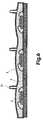
- FIG. 1is a cross-sectional view of a prior art light emitting diode
- FIG. 2is a cross-sectional view of an LED packaging process of the invention
- FIG. 3is another cross-sectional view of an LED packaging process of the invention.
- FIG. 4is a further cross-sectional view of an LED packaging process of the invention.
- FIGS. 5( a ) to 5 ( c )are schematic view of a manufacturing procedure according to another preferred embodiment of the invention.
- FIG. 6is a schematic view of a further preferred embodiment of the invention.
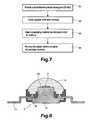
- FIG. 7is a flow chart of a manufacturing method of the invention.
- FIG. 8is a schematic view of another further preferred embodiment of the invention.
- the structure of an LED packaging process as shown in FIG. 2comprises a light emitting diode having a base 1 , an LED chip 2 , a packaging plastic shell 3 , and a packaging material 4 (as shown in FIG. 3 ).
- the base 1 of the light emitting diode in this preferred embodimentis a semi-finished product of a lead frame type LED, and the base 1 further includes a lead frame 11 for an electric connection and a heat dissipating member 12 , and then the semi-finished product is processed through a heat-resistant plastic molding injection and formation.
- the heat dissipating member 12 in the base 1has a plane 121 of the LED chip 2 , and the plane 121 fixes the LED chip 2 , and the plastic shell 3 is in a hemispherical shape for covering the base 1 and sealing the LED chip 2 in the plastic shell 3 , and the plastic shell 3 has an injection hole 31 disposed on a lateral side of the plastic shell 3 .
- the plastic shell 3is installed onto the base 1 to fully seal the space around the periphery of the LED chip 2 which is preinstalled on the base 1 , and the packaging material 4 is injected into the plastic shell 3 from the injection hole 31 .
- the packaging material 4 of this preferred embodimentis a silicone material having a hardness that falls within the range from shore A40 to shore D70, and thus after the packaging material 4 is injected from the injection hole 31 until the plastic shell 3 is filled up to form a hemispherical cover and fully cover the LED chip 2 as shown in FIG. 4 .
- the mold of the plastic shell 3 covered on the external portion of the packaging material 4is released and removed to complete the LED package structure, so that when the light emitting diode structure and other printed circuit board pass through a soldering pot in a connecting process, the light emitting diode structure and printed circuit board can resist the high temperature to successfully complete the connection.
- the foregoing processcan also be used in a printed circuit board type LED package structure as shown in FIGS. 5( a ) to 5 ( c ). Referring to FIG.
- the plastic shell 3 having a plurality of injection holes 31is covered onto a semi-finished substrate having a plurality of manufactured LED chips 2 , and injected with a packaging material 4 , and finally the mold of the plastic shell 3 is removed to complete the package structure.
- the manufacture flow of the LED packaging processcomprises the steps of providing a base 1 of the light emitting diode having an installed semi-finished product of an LED chip 2 (S 1 ); covering a plastic shell 3 onto the base 1 and fully sealing the LED chip 2 (S 2 ); injecting a packaging material into an injection hole 31 of the plastic shell 3 for the formation until the plastic shell 3 is filled up with the packaging material 4 (S 3 ); and releasing and removing the mold of the plastic shell 3 to complete the light emitting diode structure, after the packaging material 4 forms a packaging cover 11 (S 4 ).
- the base 1includes an inverted T-shaped groove 13 preinstalled at the bottom and around the periphery of the LED chip 2 , such that after the plastic shell 3 fully covers and seals the base 1 , and the packaging material 4 is injected through the injection hole 31 on the plastic shell 3 , the packaging material 4 also can be injected into the groove 13 around the periphery of the base 1 until the plastic shell 3 is filled up with the packaging material 4 and the package material is solidified to from a packaging cover, and the packaging material 4 filled in the groove 13 is solidified to form an connecting end for securing the packaging cover onto the base 1 .
Landscapes
- Engineering & Computer Science (AREA)
- Manufacturing & Machinery (AREA)
- Mechanical Engineering (AREA)
- Led Device Packages (AREA)
Abstract
Description
1. Field of the Invention
The present invention relates to a light emitting diode (LED), and more particular to a light emitting diode package structure and a method of manufacturing the same.
2. Description of Prior Art
A light emitting diode (LED) is a solid-state semiconductor device that combines two carriers produced by passing an electric current through the LED to release energy in the form of light. LED has the advantages of a compact size, a fast response rate, and a pollution-free feature, so that the LEDs can be used extensively in different industries. Since LEDs have bottlenecks including an insufficient brightness and a low luminous efficiency at an early stage, a high power LED is developed later to overcome the drawback of insufficient brightness, and thus LEDs become increasingly popular in the high power illumination market and tend to gradually take over the position of traditional tungsten lamps. LED products have the potential of replacing traditional illumination devices.
As LED manufacturing technologies are improved constantly and new materials are developed to meet the requirements of various different applications, the technology and structure of LEDs become mature, and thus leading to the development of a high power LED with enhanced energy capacity and brightness as well as the extensive use of high power LEDs in different areas. Among the types of high power LEDs, the surface mount device light emitting diode (SMD LED) is a common type of LEDs, and the general SMD LEDs are divided mainly into two types: a lead frame type and a printed circuit board type. The lead frame type uses a metal frame and a heat-resisting plastic material to produce a socket as a fixed lead frame of an LED chip by injection molding, and the printed circuit board type uses a composite material as a substrate, and both of these two types have to go through the processes of die bonding, wire bonding and encapsulation processes to complete the LED structure.
In a general die bonding process as shown inFIG. 1 , aplastic shell 101 made of an insulating heat-resistant plastic material such as epoxy resin is covered onto anLED chip 102, and a packagingplastic material 103 such as soft silicone is injected into theplastic shell 101. Such arrangement not only prevents moisture or air from being permeated into the packaging plastic material during a non-airtight packaging process of the traditional packaging process, but also uses theplastic shell 101 for receiving the injected packagingplastic material 103 to form a fixed shape of theplastic shell 101, and thus theLED chip 102 can maximize its spectrum effect by the packagingplastic material 103 and theplastic shell 101.
However, there is a major drawback of the aforementioned packaging process, since the package structure and material cannot resist high temperature, and particularly the light emitting diode and other circuit board have to be processed in a soldering pot (at 250° C.˜300° C.), and theplastic shell 101 and the softplastic material 103 usually cannot stand the high temperature of the soldering pot, and the light emitting diode structure may have broken lines or theplastic shell 101 may become soft. Even if theplastic shell 101 and the softplastic material 103 can resist the high temperature, the coefficients of thermal expansion of theplastic shell 101 and the softplastic material 103 are different, and cracks may be produced between the packagingplastic shell 101 and the softplastic material 103, and thus resulting a defective light emitting diode. To reduce the defects in a manufacturing process, the soldering is conducted manually, and thus making the manufacture more difficult and time-consuming.
In view of the foregoing shortcomings of the prior art, the inventor of the present invention based on years of experience in the related industry to conduct experiments and modifications, and finally designed a light emitting diode package structure and a method of manufacturing the same to overcome the shortcomings of the prior art structure.
The present invention is to provide a light emitting diode package structure with a heat-resisting cover and a method of manufacturing the same that adopts a heat-resistant packaging material capable of contacting air directly as a packaging cover material to improve the yield rate for the process of connecting other electronic components at a high temperature and overcome the problem of having cracks produced by the thermal expansion of traditional packaging housing and packaging material.
Accordingly, the present invention provides a light emitting diode packaging structure and a method of manufacturing the same that comprise a base, an LED chip, a plastic shell, and a packaging material, wherein the plastic shell is substantially in the shape of a bowl, and the plastic shell has an injection hole thereon. After the LED chip is installed on the base, the packaging plastic shell is covered onto the base, and the LED chip is fully and air-tightly sealed. A packaging material is injected into the plastic shell through the injection hole until the plastic shell is filled up with the packaging material to form a packaging cover, and finally the packaging plastic shell is removed to complete the LED package structure.
The features of the invention believed to be novel are set forth with particularity in the appended claims. The invention itself however may be best understood by reference to the following detailed description of the invention, which describes certain exemplary embodiments of the invention, taken in conjunction with the accompanying drawings in which:
The technical characteristics, features and advantages of the present invention will become apparent in the following detailed description of the preferred embodiments with reference to the accompanying drawings.
Referring toFIGS. 2 to 4 for the cross-sectional views of an LED packaging process according to a preferred embodiment of the present invention, the structure of an LED packaging process as shown inFIG. 2 comprises a light emitting diode having abase 1, anLED chip 2, a packagingplastic shell 3, and a packaging material4 (as shown inFIG. 3 ). Thebase 1 of the light emitting diode in this preferred embodiment is a semi-finished product of a lead frame type LED, and thebase 1 further includes alead frame 11 for an electric connection and aheat dissipating member 12, and then the semi-finished product is processed through a heat-resistant plastic molding injection and formation. Theheat dissipating member 12 in thebase 1 has aplane 121 of theLED chip 2, and theplane 121 fixes theLED chip 2, and theplastic shell 3 is in a hemispherical shape for covering thebase 1 and sealing theLED chip 2 in theplastic shell 3, and theplastic shell 3 has aninjection hole 31 disposed on a lateral side of theplastic shell 3.
InFIG. 3 , theplastic shell 3 is installed onto thebase 1 to fully seal the space around the periphery of theLED chip 2 which is preinstalled on thebase 1, and thepackaging material 4 is injected into theplastic shell 3 from theinjection hole 31. Thepackaging material 4 of this preferred embodiment is a silicone material having a hardness that falls within the range from shore A40 to shore D70, and thus after thepackaging material 4 is injected from theinjection hole 31 until theplastic shell 3 is filled up to form a hemispherical cover and fully cover theLED chip 2 as shown inFIG. 4 . After thepackaging material 4 is solidified and shaped, the mold of theplastic shell 3 covered on the external portion of thepackaging material 4 is released and removed to complete the LED package structure, so that when the light emitting diode structure and other printed circuit board pass through a soldering pot in a connecting process, the light emitting diode structure and printed circuit board can resist the high temperature to successfully complete the connection. Further, the foregoing process can also be used in a printed circuit board type LED package structure as shown inFIGS. 5( a) to5(c). Referring toFIG. 6 , theplastic shell 3 having a plurality ofinjection holes 31 is covered onto a semi-finished substrate having a plurality of manufacturedLED chips 2, and injected with apackaging material 4, and finally the mold of theplastic shell 3 is removed to complete the package structure.
Referring toFIG. 7 , the manufacture flow of the LED packaging process comprises the steps of providing abase 1 of the light emitting diode having an installed semi-finished product of an LED chip2 (S1); covering aplastic shell 3 onto thebase 1 and fully sealing the LED chip2 (S2); injecting a packaging material into aninjection hole 31 of theplastic shell 3 for the formation until theplastic shell 3 is filled up with the packaging material4 (S3); and releasing and removing the mold of theplastic shell 3 to complete the light emitting diode structure, after thepackaging material 4 forms a packaging cover11 (S4).
Referring toFIG. 8 for another preferred embodiment of the present invention, thebase 1 includes an inverted T-shaped groove 13 preinstalled at the bottom and around the periphery of theLED chip 2, such that after theplastic shell 3 fully covers and seals thebase 1, and thepackaging material 4 is injected through theinjection hole 31 on theplastic shell 3, thepackaging material 4 also can be injected into thegroove 13 around the periphery of thebase 1 until theplastic shell 3 is filled up with thepackaging material 4 and the package material is solidified to from a packaging cover, and thepackaging material 4 filled in thegroove 13 is solidified to form an connecting end for securing the packaging cover onto thebase 1.
The present invention are illustrated with reference to the preferred embodiment and not intended to limit the patent scope of the present invention. Various substitutions and modifications have suggested in the foregoing description, and other will occur to those of ordinary skill in the art. Therefore, all such substitutions and modifications are intended to be embraced within the scope of the invention as defined in the appended claims.
Claims (8)
1. A method of manufacturing a light emitting diode package structure, comprising the steps of:
providing a light emitting diode semi-finished product containing a chip;
covering a plastic shell onto a light emitting diode base, the plastic shell comprising an injection hole disposed on a lateral side thereof and opposite to the base;
injecting a packaging material from the injection hole into the plastic shell for molding; and
removing the plastic shell to complete the package structure,
wherein the base includes an inverted T-shaped groove preinstalled at the bottom and around the periphery of the chip, such that after the plastic shell fully covers and seals the base, and the packaging material is injected through the injection hole on the plastic shell, the packaging material is injected into the groove until the plastic shell is filled up with the packaging material and the package material is solidified to from a packaging cover, and the packaging material filled in the groove is solidified to form an connecting end for securing the packaging cover onto the base.
2. The method of manufacturing a light emitting diode package structure ofclaim 1 , wherein the packaging material is a silicone material.
3. The method of manufacturing a light emitting diode package structure ofclaim 1 , wherein the light emitting diode semi-finished product is a lead frame type light emitting diode.
4. The method of manufacturing a light emitting diode package structure ofclaim 1 , wherein the light emitting diode semi-finished product is a printed circuit board type light emitting diode.
5. The method of manufacturing a light emitting diode package structure ofclaim 1 , wherein the light emitting diode base further comprising a heat dissipating member, on which there is a plane for fixing the chip.
6. The method of manufacturing a light emitting diode package structure ofclaim 1 , wherein the plastic shell is in a hemispherical shape for covering the base and sealing the chip in the plastic shell.
7. The method of manufacturing a light emitting diode package structure ofclaim 1 , wherein the plastic shell is installed onto the base to fully seal the space around the periphery of the chip.
8. The method of manufacturing a light emitting diode package structure ofclaim 2 , wherein the hardness of the silicone material falls within a range from shore A40 to shore D70.
Priority Applications (1)
| Application Number | Priority Date | Filing Date | Title |
|---|---|---|---|
| US11/377,444US7808004B2 (en) | 2006-03-17 | 2006-03-17 | Light emitting diode package structure and method of manufacturing the same |
Applications Claiming Priority (1)
| Application Number | Priority Date | Filing Date | Title |
|---|---|---|---|
| US11/377,444US7808004B2 (en) | 2006-03-17 | 2006-03-17 | Light emitting diode package structure and method of manufacturing the same |
Publications (2)
| Publication Number | Publication Date |
|---|---|
| US20070215896A1 US20070215896A1 (en) | 2007-09-20 |
| US7808004B2true US7808004B2 (en) | 2010-10-05 |
Family
ID=38516872
Family Applications (1)
| Application Number | Title | Priority Date | Filing Date |
|---|---|---|---|
| US11/377,444Expired - Fee RelatedUS7808004B2 (en) | 2006-03-17 | 2006-03-17 | Light emitting diode package structure and method of manufacturing the same |
Country Status (1)
| Country | Link |
|---|---|
| US (1) | US7808004B2 (en) |
Cited By (6)
| Publication number | Priority date | Publication date | Assignee | Title |
|---|---|---|---|---|
| US20100148377A1 (en)* | 2008-12-15 | 2010-06-17 | Elpida Memory, Inc. | Intermediate structure of semiconductor device and method of manufacturing the same |
| US20100213487A1 (en)* | 2009-02-24 | 2010-08-26 | Advanced Optoelectronic Technology, Inc. | Side-emitting led package and manufacturing method of the same |
| US20120307491A1 (en)* | 2011-06-03 | 2012-12-06 | Shanghai Sansi Electronics Engineering Co., Ltd. | Illumination device |
| US8585248B1 (en)* | 2010-08-16 | 2013-11-19 | NuLEDs, Inc. | LED luminaire having heat sinking panels |
| US20150338067A1 (en)* | 2013-01-31 | 2015-11-26 | Panasonic Intellectual Property Management Co., Ltd. | Electronic circuit device and method for manufacturing electronic circuit device |
| US9644833B1 (en) | 2013-10-04 | 2017-05-09 | Universal Lighting Technologies, Inc. | Encapsulated LED lighting module with integral gas venting |
Families Citing this family (10)
| Publication number | Priority date | Publication date | Assignee | Title |
|---|---|---|---|---|
| DE102007046520A1 (en)* | 2007-09-28 | 2009-04-02 | Osram Opto Semiconductors Gmbh | Light-emitting surface element and method for producing a light-emitting surface element |
| KR101488448B1 (en)* | 2007-12-06 | 2015-02-02 | 서울반도체 주식회사 | LED package and manufacturing method thereof |
| TWI399872B (en)* | 2009-03-06 | 2013-06-21 | I Chiun Precision Ind Co Ltd | Light emitting diode package structure and manufacturing process thereof |
| JP5767062B2 (en)* | 2010-09-30 | 2015-08-19 | 日東電工株式会社 | Light emitting diode sealing material and method for manufacturing light emitting diode device |
| US9431592B2 (en) | 2011-06-01 | 2016-08-30 | The Hong Kong University Of Science And Technology | Submount with cavities and through vias for LED packaging |
| US9095208B1 (en) | 2011-11-28 | 2015-08-04 | Agio International Company, Limited | Tabletop system |
| US8895994B2 (en)* | 2012-06-27 | 2014-11-25 | Schlumberger Technology Corporation | Electronic device including silicon carbide diode dies |
| CN203707181U (en)* | 2014-02-21 | 2014-07-09 | 厦门市三安光电科技有限公司 | Light emitting diode packaging body |
| US11600754B2 (en)* | 2018-11-29 | 2023-03-07 | Lumileds Llc | Light-emitting device and method of packaging the same |
| WO2020109023A1 (en)* | 2018-11-29 | 2020-06-04 | Lumileds Holding B.V. | Light-emitting device and method of packaging the same |
Citations (64)
| Publication number | Priority date | Publication date | Assignee | Title |
|---|---|---|---|---|
| US3192536A (en)* | 1963-10-28 | 1965-07-06 | Air Reduction | Headgear and hammock assembly connecting means therefor |
| US4701999A (en)* | 1985-12-17 | 1987-10-27 | Pnc, Inc. | Method of making sealed housings containing delicate structures |
| US4823605A (en)* | 1987-03-18 | 1989-04-25 | Siemens Aktiengesellschaft | Semiconductor pressure sensor with casing and method for its manufacture |
| US4942140A (en)* | 1987-03-25 | 1990-07-17 | Mitsubishi Denki Kabushiki Kaisha | Method of packaging semiconductor device |
| US5218759A (en)* | 1991-03-18 | 1993-06-15 | Motorola, Inc. | Method of making a transfer molded semiconductor device |
| US5329131A (en)* | 1991-05-17 | 1994-07-12 | U.S. Philips Corporation | Opto-electronic coupler having improved moisture protective housing |
| US5434105A (en)* | 1994-03-04 | 1995-07-18 | National Semiconductor Corporation | Process for attaching a lead frame to a heat sink using a glob-top encapsulation |
| US5570272A (en)* | 1993-08-18 | 1996-10-29 | Lsi Logic Corporation | Apparatus for encapsulating an integrated circuit package |
| US5663106A (en)* | 1994-05-19 | 1997-09-02 | Tessera, Inc. | Method of encapsulating die and chip carrier |
| US5687270A (en)* | 1994-10-27 | 1997-11-11 | Nec Corporation | Photodetector module capable of preventing deviation of optical axis |
| US5863810A (en)* | 1994-05-09 | 1999-01-26 | Euratec B.V. | Method for encapsulating an integrated circuit having a window |
| US5959316A (en)* | 1998-09-01 | 1999-09-28 | Hewlett-Packard Company | Multiple encapsulation of phosphor-LED devices |
| US5981312A (en)* | 1997-06-27 | 1999-11-09 | International Business Machines Corporation | Method for injection molded flip chip encapsulation |
| US6081997A (en)* | 1997-08-14 | 2000-07-04 | Lsi Logic Corporation | System and method for packaging an integrated circuit using encapsulant injection |
| US6135850A (en)* | 1997-12-29 | 2000-10-24 | Reed; Gerald D. | Lighted toy and safety method |
| US6139304A (en)* | 1996-12-10 | 2000-10-31 | Itt Manufacturing Enterprises, Inc. | Mold for injection molding encapsulation over small device on substrate |
| US6155699A (en)* | 1999-03-15 | 2000-12-05 | Agilent Technologies, Inc. | Efficient phosphor-conversion led structure |
| US6245259B1 (en)* | 1996-09-20 | 2001-06-12 | Osram Opto Semiconductors, Gmbh & Co. Ohg | Wavelength-converting casting composition and light-emitting semiconductor component |
| US6254815B1 (en)* | 1994-07-29 | 2001-07-03 | Motorola, Inc. | Molded packaging method for a sensing die having a pressure sensing diaphragm |
| US20010023087A1 (en)* | 2000-03-14 | 2001-09-20 | Manfred Brandl | Method for housing sensors in a package |
| US20010030866A1 (en)* | 2000-03-31 | 2001-10-18 | Relume Corporation | LED integrated heat sink |
| US20020076856A1 (en)* | 1997-02-25 | 2002-06-20 | Wensel Richard W. | Method and apparatus for transfer molding encapsulation of a semiconductor die with attached heat sink |
| US20020163001A1 (en)* | 2001-05-04 | 2002-11-07 | Shaddock David Mulford | Surface mount light emitting device package and fabrication method |
| US6480389B1 (en)* | 2002-01-04 | 2002-11-12 | Opto Tech Corporation | Heat dissipation structure for solid-state light emitting device package |
| US20030025117A1 (en)* | 2001-07-19 | 2003-02-06 | Shinji Isokawa | Semiconductor light-emitting device having a reflective case |
| US6541800B2 (en)* | 2001-02-22 | 2003-04-01 | Weldon Technologies, Inc. | High power LED |
| US6552263B2 (en)* | 1997-06-27 | 2003-04-22 | International Business Machines Corporation | Method of injection molded flip chip encapsulation |
| US6572280B2 (en)* | 2000-01-18 | 2003-06-03 | Infineon Technologies Ag | Optical transmitting/receiving module including an internal optical waveguide |
| US20030168720A1 (en)* | 2002-03-06 | 2003-09-11 | Nichia Corporation | Semiconductor device and manufacturing method for same |
| US20030185005A1 (en)* | 2002-04-01 | 2003-10-02 | Gelcore, Llc | Light emitting diode-based signal light |
| US20030211804A1 (en)* | 1999-04-22 | 2003-11-13 | Osram Opto Semiconductors Gmbh & Co. Ohg | LED light source with lens and corresponding production method |
| US20040008952A1 (en)* | 2000-12-29 | 2004-01-15 | Hans Kragl | Coupling device for optically coupling an optical waveguide to an elecro-optical element |
| US6692987B2 (en)* | 2001-12-12 | 2004-02-17 | Micron Technology, Inc. | BOC BGA package for die with I-shaped bond pad layout |
| US20040079957A1 (en)* | 2002-09-04 | 2004-04-29 | Andrews Peter Scott | Power surface mount light emitting die package |
| US6734465B1 (en)* | 2001-11-19 | 2004-05-11 | Nanocrystals Technology Lp | Nanocrystalline based phosphors and photonic structures for solid state lighting |
| US6733711B2 (en)* | 2000-09-01 | 2004-05-11 | General Electric Company | Plastic packaging of LED arrays |
| US6751327B1 (en)* | 2000-07-11 | 2004-06-15 | Insonus Medical, Inc. | Miniature plastic battery assembly for canal hearing devices |
| US20040119086A1 (en)* | 2002-11-25 | 2004-06-24 | Matsushita Electric Industrial Co. Ltd. | Led Lamp |
| US6767767B2 (en)* | 2001-08-31 | 2004-07-27 | Renesas Technology Corp. | Method of manufacturing a semiconductor device in which a block molding package utilizes air vents in a substrate |
| US20040169466A1 (en)* | 2002-12-24 | 2004-09-02 | Toyoda Gosei Co., Ltd. | Light emitting diode and light emitting diode array |
| US20040183081A1 (en)* | 2003-03-20 | 2004-09-23 | Alexander Shishov | Light emitting diode package with self dosing feature and methods of forming same |
| US6826336B2 (en)* | 2002-05-22 | 2004-11-30 | The Boeing Company | Fiber optic LED illuminator |
| US6922024B2 (en)* | 2002-11-25 | 2005-07-26 | Matsushita Electric Industrial Co., Ltd. | LED lamp |
| US6936855B1 (en)* | 2002-01-16 | 2005-08-30 | Shane Harrah | Bendable high flux LED array |
| US20050202826A1 (en)* | 2004-03-12 | 2005-09-15 | Coretek Opto Corp. | Optical subassembly |
| US20050224821A1 (en)* | 2001-01-24 | 2005-10-13 | Nichia Corporation | Light emitting diode, optical semiconductor device, epoxy resin composition suited for optical semiconductor device, and method for manufacturing the same |
| US20050230691A1 (en)* | 2004-04-15 | 2005-10-20 | Marco Amiotti | Integrated getter for vacuum or inert gas packaged LEDs |
| US20050236638A1 (en)* | 2003-03-27 | 2005-10-27 | Sanken Electric Co., Ltd. | Semiconductor light emitting device |
| US20050276438A1 (en)* | 2004-03-25 | 2005-12-15 | Hiroyuki Kobayashi | Speaker device and method of manufacturing the speaker device |
| US7029935B2 (en)* | 2003-09-09 | 2006-04-18 | Cree, Inc. | Transmissive optical elements including transparent plastic shell having a phosphor dispersed therein, and methods of fabricating same |
| US7080787B2 (en)* | 2003-07-03 | 2006-07-25 | Symbol Technologies, Inc. | Insert molded antenna |
| US20060186423A1 (en)* | 2003-05-05 | 2006-08-24 | Greg Blonder | Method of making optical light engines with elevated LEDs and resulting product |
| US20060267041A1 (en)* | 2005-05-27 | 2006-11-30 | Para Light Electronics Co., Ltd. | High-brightness light-emitting diode |
| US7145253B1 (en)* | 2004-06-09 | 2006-12-05 | Amkor Technology, Inc. | Encapsulated sensor device |
| US20060284185A1 (en)* | 2004-04-07 | 2006-12-21 | Chang-Hae Kim | Light emitting device and phosphor for the same |
| US20070017294A1 (en)* | 2005-07-22 | 2007-01-25 | Mitsubishi Denki Kabushiki Kaisha | Semiconductor pressure sensor |
| US7213945B2 (en)* | 2002-05-17 | 2007-05-08 | Ccs, Inc. | Light emitting diode and method for fabricating the same |
| US20070140624A1 (en)* | 2005-10-11 | 2007-06-21 | Hong Kong Applied Science And Technology Research Institute Co., Ltd. | Opto-electronic device for optical fibre applications |
| US7264378B2 (en)* | 2002-09-04 | 2007-09-04 | Cree, Inc. | Power surface mount light emitting die package |
| US7276739B2 (en)* | 2004-03-11 | 2007-10-02 | Chen-Lun Hsin Chen | Low thermal resistance light emitting diode |
| US7321161B2 (en)* | 2003-12-19 | 2008-01-22 | Philips Lumileds Lighting Company, Llc | LED package assembly with datum reference feature |
| US7326583B2 (en)* | 2004-03-31 | 2008-02-05 | Cree, Inc. | Methods for packaging of a semiconductor light emitting device |
| US20080268559A1 (en)* | 2005-07-13 | 2008-10-30 | Seoul Semiconductor Co., Ltd. | Mold for Forming a Molding Member and Method of Fabricating a Molding Member Using the Same |
| US7498610B2 (en)* | 2005-02-17 | 2009-03-03 | Samsung Electro-Mechanics Co., Ltd. | High power LED housing and fabrication method thereof |
- 2006
- 2006-03-17USUS11/377,444patent/US7808004B2/ennot_activeExpired - Fee Related
Patent Citations (66)
| Publication number | Priority date | Publication date | Assignee | Title |
|---|---|---|---|---|
| US3192536A (en)* | 1963-10-28 | 1965-07-06 | Air Reduction | Headgear and hammock assembly connecting means therefor |
| US4701999A (en)* | 1985-12-17 | 1987-10-27 | Pnc, Inc. | Method of making sealed housings containing delicate structures |
| US4823605A (en)* | 1987-03-18 | 1989-04-25 | Siemens Aktiengesellschaft | Semiconductor pressure sensor with casing and method for its manufacture |
| US4942140A (en)* | 1987-03-25 | 1990-07-17 | Mitsubishi Denki Kabushiki Kaisha | Method of packaging semiconductor device |
| US5218759A (en)* | 1991-03-18 | 1993-06-15 | Motorola, Inc. | Method of making a transfer molded semiconductor device |
| US5329131A (en)* | 1991-05-17 | 1994-07-12 | U.S. Philips Corporation | Opto-electronic coupler having improved moisture protective housing |
| US5570272A (en)* | 1993-08-18 | 1996-10-29 | Lsi Logic Corporation | Apparatus for encapsulating an integrated circuit package |
| US5434105A (en)* | 1994-03-04 | 1995-07-18 | National Semiconductor Corporation | Process for attaching a lead frame to a heat sink using a glob-top encapsulation |
| US5863810A (en)* | 1994-05-09 | 1999-01-26 | Euratec B.V. | Method for encapsulating an integrated circuit having a window |
| US5663106A (en)* | 1994-05-19 | 1997-09-02 | Tessera, Inc. | Method of encapsulating die and chip carrier |
| US6254815B1 (en)* | 1994-07-29 | 2001-07-03 | Motorola, Inc. | Molded packaging method for a sensing die having a pressure sensing diaphragm |
| US5687270A (en)* | 1994-10-27 | 1997-11-11 | Nec Corporation | Photodetector module capable of preventing deviation of optical axis |
| US6245259B1 (en)* | 1996-09-20 | 2001-06-12 | Osram Opto Semiconductors, Gmbh & Co. Ohg | Wavelength-converting casting composition and light-emitting semiconductor component |
| US6139304A (en)* | 1996-12-10 | 2000-10-31 | Itt Manufacturing Enterprises, Inc. | Mold for injection molding encapsulation over small device on substrate |
| US6617786B1 (en)* | 1996-12-10 | 2003-09-09 | Itt Industries | Electronic device encapsulated directly on a substrate |
| US20020076856A1 (en)* | 1997-02-25 | 2002-06-20 | Wensel Richard W. | Method and apparatus for transfer molding encapsulation of a semiconductor die with attached heat sink |
| US5981312A (en)* | 1997-06-27 | 1999-11-09 | International Business Machines Corporation | Method for injection molded flip chip encapsulation |
| US6552263B2 (en)* | 1997-06-27 | 2003-04-22 | International Business Machines Corporation | Method of injection molded flip chip encapsulation |
| US6081997A (en)* | 1997-08-14 | 2000-07-04 | Lsi Logic Corporation | System and method for packaging an integrated circuit using encapsulant injection |
| US6135850A (en)* | 1997-12-29 | 2000-10-24 | Reed; Gerald D. | Lighted toy and safety method |
| US5959316A (en)* | 1998-09-01 | 1999-09-28 | Hewlett-Packard Company | Multiple encapsulation of phosphor-LED devices |
| US6155699A (en)* | 1999-03-15 | 2000-12-05 | Agilent Technologies, Inc. | Efficient phosphor-conversion led structure |
| US20030211804A1 (en)* | 1999-04-22 | 2003-11-13 | Osram Opto Semiconductors Gmbh & Co. Ohg | LED light source with lens and corresponding production method |
| US6572280B2 (en)* | 2000-01-18 | 2003-06-03 | Infineon Technologies Ag | Optical transmitting/receiving module including an internal optical waveguide |
| US20010023087A1 (en)* | 2000-03-14 | 2001-09-20 | Manfred Brandl | Method for housing sensors in a package |
| US20010030866A1 (en)* | 2000-03-31 | 2001-10-18 | Relume Corporation | LED integrated heat sink |
| US6751327B1 (en)* | 2000-07-11 | 2004-06-15 | Insonus Medical, Inc. | Miniature plastic battery assembly for canal hearing devices |
| US6733711B2 (en)* | 2000-09-01 | 2004-05-11 | General Electric Company | Plastic packaging of LED arrays |
| US20040008952A1 (en)* | 2000-12-29 | 2004-01-15 | Hans Kragl | Coupling device for optically coupling an optical waveguide to an elecro-optical element |
| US20050224821A1 (en)* | 2001-01-24 | 2005-10-13 | Nichia Corporation | Light emitting diode, optical semiconductor device, epoxy resin composition suited for optical semiconductor device, and method for manufacturing the same |
| US6541800B2 (en)* | 2001-02-22 | 2003-04-01 | Weldon Technologies, Inc. | High power LED |
| US20020163001A1 (en)* | 2001-05-04 | 2002-11-07 | Shaddock David Mulford | Surface mount light emitting device package and fabrication method |
| US20030025117A1 (en)* | 2001-07-19 | 2003-02-06 | Shinji Isokawa | Semiconductor light-emitting device having a reflective case |
| US6767767B2 (en)* | 2001-08-31 | 2004-07-27 | Renesas Technology Corp. | Method of manufacturing a semiconductor device in which a block molding package utilizes air vents in a substrate |
| US7259400B1 (en)* | 2001-11-19 | 2007-08-21 | Nanocrystal Lighting Corporation | Nanocomposite photonic structures for solid state lighting |
| US6734465B1 (en)* | 2001-11-19 | 2004-05-11 | Nanocrystals Technology Lp | Nanocrystalline based phosphors and photonic structures for solid state lighting |
| US6692987B2 (en)* | 2001-12-12 | 2004-02-17 | Micron Technology, Inc. | BOC BGA package for die with I-shaped bond pad layout |
| US6480389B1 (en)* | 2002-01-04 | 2002-11-12 | Opto Tech Corporation | Heat dissipation structure for solid-state light emitting device package |
| US6936855B1 (en)* | 2002-01-16 | 2005-08-30 | Shane Harrah | Bendable high flux LED array |
| US20030168720A1 (en)* | 2002-03-06 | 2003-09-11 | Nichia Corporation | Semiconductor device and manufacturing method for same |
| US20030185005A1 (en)* | 2002-04-01 | 2003-10-02 | Gelcore, Llc | Light emitting diode-based signal light |
| US7213945B2 (en)* | 2002-05-17 | 2007-05-08 | Ccs, Inc. | Light emitting diode and method for fabricating the same |
| US6826336B2 (en)* | 2002-05-22 | 2004-11-30 | The Boeing Company | Fiber optic LED illuminator |
| US7264378B2 (en)* | 2002-09-04 | 2007-09-04 | Cree, Inc. | Power surface mount light emitting die package |
| US20040079957A1 (en)* | 2002-09-04 | 2004-04-29 | Andrews Peter Scott | Power surface mount light emitting die package |
| US6922024B2 (en)* | 2002-11-25 | 2005-07-26 | Matsushita Electric Industrial Co., Ltd. | LED lamp |
| US20040119086A1 (en)* | 2002-11-25 | 2004-06-24 | Matsushita Electric Industrial Co. Ltd. | Led Lamp |
| US20040169466A1 (en)* | 2002-12-24 | 2004-09-02 | Toyoda Gosei Co., Ltd. | Light emitting diode and light emitting diode array |
| US20040183081A1 (en)* | 2003-03-20 | 2004-09-23 | Alexander Shishov | Light emitting diode package with self dosing feature and methods of forming same |
| US20050236638A1 (en)* | 2003-03-27 | 2005-10-27 | Sanken Electric Co., Ltd. | Semiconductor light emitting device |
| US20060186423A1 (en)* | 2003-05-05 | 2006-08-24 | Greg Blonder | Method of making optical light engines with elevated LEDs and resulting product |
| US7080787B2 (en)* | 2003-07-03 | 2006-07-25 | Symbol Technologies, Inc. | Insert molded antenna |
| US7029935B2 (en)* | 2003-09-09 | 2006-04-18 | Cree, Inc. | Transmissive optical elements including transparent plastic shell having a phosphor dispersed therein, and methods of fabricating same |
| US7321161B2 (en)* | 2003-12-19 | 2008-01-22 | Philips Lumileds Lighting Company, Llc | LED package assembly with datum reference feature |
| US7276739B2 (en)* | 2004-03-11 | 2007-10-02 | Chen-Lun Hsin Chen | Low thermal resistance light emitting diode |
| US20050202826A1 (en)* | 2004-03-12 | 2005-09-15 | Coretek Opto Corp. | Optical subassembly |
| US20050276438A1 (en)* | 2004-03-25 | 2005-12-15 | Hiroyuki Kobayashi | Speaker device and method of manufacturing the speaker device |
| US7326583B2 (en)* | 2004-03-31 | 2008-02-05 | Cree, Inc. | Methods for packaging of a semiconductor light emitting device |
| US20060284185A1 (en)* | 2004-04-07 | 2006-12-21 | Chang-Hae Kim | Light emitting device and phosphor for the same |
| US20050230691A1 (en)* | 2004-04-15 | 2005-10-20 | Marco Amiotti | Integrated getter for vacuum or inert gas packaged LEDs |
| US7145253B1 (en)* | 2004-06-09 | 2006-12-05 | Amkor Technology, Inc. | Encapsulated sensor device |
| US7498610B2 (en)* | 2005-02-17 | 2009-03-03 | Samsung Electro-Mechanics Co., Ltd. | High power LED housing and fabrication method thereof |
| US20060267041A1 (en)* | 2005-05-27 | 2006-11-30 | Para Light Electronics Co., Ltd. | High-brightness light-emitting diode |
| US20080268559A1 (en)* | 2005-07-13 | 2008-10-30 | Seoul Semiconductor Co., Ltd. | Mold for Forming a Molding Member and Method of Fabricating a Molding Member Using the Same |
| US20070017294A1 (en)* | 2005-07-22 | 2007-01-25 | Mitsubishi Denki Kabushiki Kaisha | Semiconductor pressure sensor |
| US20070140624A1 (en)* | 2005-10-11 | 2007-06-21 | Hong Kong Applied Science And Technology Research Institute Co., Ltd. | Opto-electronic device for optical fibre applications |
Cited By (10)
| Publication number | Priority date | Publication date | Assignee | Title |
|---|---|---|---|---|
| US20100148377A1 (en)* | 2008-12-15 | 2010-06-17 | Elpida Memory, Inc. | Intermediate structure of semiconductor device and method of manufacturing the same |
| US8198141B2 (en)* | 2008-12-15 | 2012-06-12 | Elpida Memory, Inc. | Intermediate structure of semiconductor device and method of manufacturing the same |
| US20100213487A1 (en)* | 2009-02-24 | 2010-08-26 | Advanced Optoelectronic Technology, Inc. | Side-emitting led package and manufacturing method of the same |
| US8089089B2 (en)* | 2009-02-24 | 2012-01-03 | Advanced Optoelectronic Technology, Inc. | Side-emitting LED package and manufacturing method of the same |
| US8585248B1 (en)* | 2010-08-16 | 2013-11-19 | NuLEDs, Inc. | LED luminaire having heat sinking panels |
| US20120307491A1 (en)* | 2011-06-03 | 2012-12-06 | Shanghai Sansi Electronics Engineering Co., Ltd. | Illumination device |
| US8517569B2 (en)* | 2011-06-03 | 2013-08-27 | Shanghai Sansi Electronics Engineering Co., Ltd. | Illumination device |
| US20150338067A1 (en)* | 2013-01-31 | 2015-11-26 | Panasonic Intellectual Property Management Co., Ltd. | Electronic circuit device and method for manufacturing electronic circuit device |
| US9568169B2 (en)* | 2013-01-31 | 2017-02-14 | Panasonic Intellectual Property Management Co., Ltd. | Electronic circuit device and method for manufacturing electronic circuit device |
| US9644833B1 (en) | 2013-10-04 | 2017-05-09 | Universal Lighting Technologies, Inc. | Encapsulated LED lighting module with integral gas venting |
Also Published As
| Publication number | Publication date |
|---|---|
| US20070215896A1 (en) | 2007-09-20 |
Similar Documents
| Publication | Publication Date | Title |
|---|---|---|
| US7808004B2 (en) | Light emitting diode package structure and method of manufacturing the same | |
| CN100546058C (en) | Power luminous diode packaging structure | |
| US8076182B2 (en) | Method of making a semiconductor chip assembly with a post/base heat spreader and a cavity over the post | |
| US8324723B2 (en) | Semiconductor chip assembly with bump/base heat spreader and dual-angle cavity in bump | |
| CN101222010B (en) | Photoelectric component packaging structure and packaging method | |
| US8193556B2 (en) | Semiconductor chip assembly with post/base heat spreader and cavity in post | |
| US8207553B2 (en) | Semiconductor chip assembly with base heat spreader and cavity in base | |
| US8455275B2 (en) | Method for making light emitting diode package | |
| US8314438B2 (en) | Semiconductor chip assembly with bump/base heat spreader and cavity in bump | |
| CN101937962A (en) | A kind of LED packaging structure and packaging method thereof | |
| US8415703B2 (en) | Semiconductor chip assembly with post/base/flange heat spreader and cavity in flange | |
| CN102738365A (en) | Novel LED (Light Emitting Diode) packaging piece based on DFN (Double Flat No-lead package) and QFN (Quad Flat No-lead Package), and manufacturing method of packaging piece | |
| US8658445B2 (en) | Method for manufacturing phosphor film and method for making LED package having the phosphor film | |
| CN102104012B (en) | Manufacturing method of light-emitting diode | |
| CN203377266U (en) | Flexible COB (chip on board) packaging LED | |
| CN103606545B (en) | LED flexible board light source module and manufacturing method thereof | |
| TWI424549B (en) | Improved wire diode package and manufacturing method thereof | |
| US20110233598A1 (en) | Light emitting diode package and manufacturing method thereof | |
| CN103633235A (en) | LED module and manufacturing process thereof | |
| CN101847684B (en) | Packaged circuit board with enhanced heat dissipation effect and manufacturing method thereof | |
| CN104791734A (en) | Heat sink with embedded circuit, manufacturing method thereof, LED module and manufacturing method thereof | |
| TWI299916B (en) | ||
| CN203799604U (en) | LED display unit module with enhanced heat dissipation performance | |
| CN207265094U (en) | Point light source, integrated optical circuit and electronic device | |
| CN2798315Y (en) | High power LED packing structure |
Legal Events
| Date | Code | Title | Description |
|---|---|---|---|
| AS | Assignment | Owner name:EDISON OPTO CORPORATION, TAIWAN Free format text:ASSIGNMENT OF ASSIGNORS INTEREST;ASSIGNORS:SUN, TSUNG-TING;LAIO, HUNG-TA;CHOU, HUNG-HSUN;AND OTHERS;REEL/FRAME:017699/0684 Effective date:20060109 | |
| STCF | Information on status: patent grant | Free format text:PATENTED CASE | |
| FPAY | Fee payment | Year of fee payment:4 | |
| MAFP | Maintenance fee payment | Free format text:PAYMENT OF MAINTENANCE FEE, 8TH YEAR, LARGE ENTITY (ORIGINAL EVENT CODE: M1552) Year of fee payment:8 | |
| FEPP | Fee payment procedure | Free format text:MAINTENANCE FEE REMINDER MAILED (ORIGINAL EVENT CODE: REM.); ENTITY STATUS OF PATENT OWNER: LARGE ENTITY | |
| LAPS | Lapse for failure to pay maintenance fees | Free format text:PATENT EXPIRED FOR FAILURE TO PAY MAINTENANCE FEES (ORIGINAL EVENT CODE: EXP.); ENTITY STATUS OF PATENT OWNER: LARGE ENTITY | |
| STCH | Information on status: patent discontinuation | Free format text:PATENT EXPIRED DUE TO NONPAYMENT OF MAINTENANCE FEES UNDER 37 CFR 1.362 | |
| FP | Lapsed due to failure to pay maintenance fee | Effective date:20221005 |