US7807575B2 - Methods to reduce the critical dimension of semiconductor devices - Google Patents
Methods to reduce the critical dimension of semiconductor devicesDownload PDFInfo
- Publication number
- US7807575B2 US7807575B2US11/606,613US60661306AUS7807575B2US 7807575 B2US7807575 B2US 7807575B2US 60661306 AUS60661306 AUS 60661306AUS 7807575 B2US7807575 B2US 7807575B2
- Authority
- US
- United States
- Prior art keywords
- layer
- spacers
- portions
- resist layer
- forming
- Prior art date
- Legal status (The legal status is an assumption and is not a legal conclusion. Google has not performed a legal analysis and makes no representation as to the accuracy of the status listed.)
- Active, expires
Links
Images


Classifications
- H—ELECTRICITY
- H01—ELECTRIC ELEMENTS
- H01L—SEMICONDUCTOR DEVICES NOT COVERED BY CLASS H10
- H01L21/00—Processes or apparatus adapted for the manufacture or treatment of semiconductor or solid state devices or of parts thereof
- H01L21/02—Manufacture or treatment of semiconductor devices or of parts thereof
- H01L21/027—Making masks on semiconductor bodies for further photolithographic processing not provided for in group H01L21/18 or H01L21/34
- H01L21/033—Making masks on semiconductor bodies for further photolithographic processing not provided for in group H01L21/18 or H01L21/34 comprising inorganic layers
- H01L21/0334—Making masks on semiconductor bodies for further photolithographic processing not provided for in group H01L21/18 or H01L21/34 comprising inorganic layers characterised by their size, orientation, disposition, behaviour, shape, in horizontal or vertical plane
- H01L21/0338—Process specially adapted to improve the resolution of the mask
- H—ELECTRICITY
- H01—ELECTRIC ELEMENTS
- H01L—SEMICONDUCTOR DEVICES NOT COVERED BY CLASS H10
- H01L21/00—Processes or apparatus adapted for the manufacture or treatment of semiconductor or solid state devices or of parts thereof
- H01L21/02—Manufacture or treatment of semiconductor devices or of parts thereof
- H01L21/027—Making masks on semiconductor bodies for further photolithographic processing not provided for in group H01L21/18 or H01L21/34
- H01L21/033—Making masks on semiconductor bodies for further photolithographic processing not provided for in group H01L21/18 or H01L21/34 comprising inorganic layers
- H—ELECTRICITY
- H01—ELECTRIC ELEMENTS
- H01L—SEMICONDUCTOR DEVICES NOT COVERED BY CLASS H10
- H01L21/00—Processes or apparatus adapted for the manufacture or treatment of semiconductor or solid state devices or of parts thereof
- H01L21/02—Manufacture or treatment of semiconductor devices or of parts thereof
- H01L21/04—Manufacture or treatment of semiconductor devices or of parts thereof the devices having potential barriers, e.g. a PN junction, depletion layer or carrier concentration layer
- H01L21/18—Manufacture or treatment of semiconductor devices or of parts thereof the devices having potential barriers, e.g. a PN junction, depletion layer or carrier concentration layer the devices having semiconductor bodies comprising elements of Group IV of the Periodic Table or AIIIBV compounds with or without impurities, e.g. doping materials
- H01L21/30—Treatment of semiconductor bodies using processes or apparatus not provided for in groups H01L21/20 - H01L21/26
- H01L21/302—Treatment of semiconductor bodies using processes or apparatus not provided for in groups H01L21/20 - H01L21/26 to change their surface-physical characteristics or shape, e.g. etching, polishing, cutting
- H01L21/306—Chemical or electrical treatment, e.g. electrolytic etching
- H01L21/308—Chemical or electrical treatment, e.g. electrolytic etching using masks
- H01L21/3083—Chemical or electrical treatment, e.g. electrolytic etching using masks characterised by their size, orientation, disposition, behaviour, shape, in horizontal or vertical plane
- H01L21/3088—Process specially adapted to improve the resolution of the mask
Definitions
- Embodiments of the present inventionrelate generally to the fabrication of semiconductor devices and, more specifically, to methods for reducing the critical dimension (CD) of semiconductor devices and to partially fabricated semiconductor devices having reduced critical dimensions.
- CDcritical dimension
- These featuresare typically defined by openings in, and spaced from each other by, a material, such as an insulator or conductor.
- the distance between identical points in neighboring featuresis referred to in the industry as “pitch.”
- the pitchis typically measured as the center-to-center distance between the features.
- pitchis about equal to the sum of the width of a feature and of the width of the space separating that feature from a neighboring feature.
- the width of the featureis also referred to as the CD or minimum feature size (“F”) of the line.
- the CDis typically the smallest geometrical feature, such as the width of an interconnect line, contact, or trench, that is formed during IC manufacturing using a given technology, such as photolithography. Because the width of the space adjacent to the feature is typically equal to the width of the feature, the pitch of the feature is typically two times the feature size (2F).
- a partially expendable stringer layeris conformally deposited over the mandrel strips and etched to form stringer strips having a thickness of F/2 on sidewalls of the mandrel strips.
- the mandrel stripsare etched while the stringer strips remain on the semiconductor substrate.
- the stringer stripsfunction as a mask to etch trenches having a width of F/2 in the semiconductor substrate. While the pitch in the above-mentioned patent is actually halved, such a reduction in pitch is referred to in the industry as “pitch doubling” or “pitch multiplication.” In other words, “multiplication” of pitch by a certain factor involves reducing the pitch by that factor. This conventional terminology is retained herein.
- U.S. Pat. No. 6,239,008discloses a method of pitch doubling.
- a photoresistis patterned over a semiconductor material layer. The dimension of one photoresist structure and one adjoining space is defined as x.
- the photoresist structuresare trimmed to 1 ⁇ 2 x.
- the spaces between structuresare increased to 3 ⁇ 4 x.
- the exposed portions of the semiconductor material layerare etched forming structures in the semiconductor material layer.
- the photoresist structuresare removed.
- a blanket layeris deposited over the semiconductor material layer structures.
- the blanket layeris etched to form spacers on the sidewalls of the semiconductor material layer structures.
- a second blanket layeris deposited over the semiconductor material layer structures, the spacers, and the spaces, forming a second set of structures in the spaces.
- the second blanket layeris a material similar to, or the same as, the material from which the semiconductor material layer structures are made.
- the semiconductor material layer structures, the spacers, and the second set of structuresare planarized.
- the spacersare removed.
- the semiconductor material layer structures and the second set of structures and the spaces therebetweenhave a dimension of 1 ⁇ 4 x.
- U.S. Pat. No. 6,638,441discloses a method of pitch tripling.
- a photoresist layeris patterned on a substrate.
- a layeris formed over the pattern.
- the first layeris etched to expose the substrate.
- a second layeris formed over the pattern.
- the second layeris etched to expose the substrate.
- the patterned resistis removed.
- a third layeris formed over the first and second layers and the substrate.
- the third layeris etched to expose the substrate.
- a fourth layeris formed over the first, second, and third layers and the substrate.
- the material of the fourth layeris the same as the material of the first layer.
- the fourth layeris etched to expose the first, second, and third layers.
- the second and third layersare removed.
- the first and fourth layersform a pattern with a pitch that has been tripled.
- 193 nm photolithographyis able to form smaller features than 248 nm photolithography.
- 193 nm photoresist materialshave increased line edge roughness (LER) compared to 248 nm photoresist materials.
- 248 nm photoresist materialsare stronger than 193 nm photoresist materials.
- FIG. 1illustrates an embodiment of an intermediate layer, an anti-reflective layer, and a resist layer formed over a target layer on a partially fabricated integrated circuit device
- FIG. 2illustrates an embodiment of the resist layer of FIG. 1 patterned with a desired CD
- FIG. 3illustrates an embodiment of a first spacer layer formed over the features of FIG. 2 ;
- FIG. 4illustrates an embodiment of first spacers formed from the first spacer layer of FIG. 3 ;
- FIG. 5illustrates an embodiment of the partially fabricated integrated circuit device of FIG. 4 after the features of FIG. 2 have been removed;
- FIG. 6illustrates an embodiment of the partially fabricated integrated circuit device of FIG. 5 after portions of the intermediate layer and the anti-reflective layer have been removed;
- FIG. 7illustrates an embodiment of the partially fabricated integrated circuit device of FIG. 6 after the first spacers and the anti-reflective layer have been removed;
- FIG. 8illustrates an embodiment of a second spacer layer formed over the partially fabricated integrated circuit device of FIG. 7 ;
- FIG. 9illustrates an embodiment of the partially fabricated integrated circuit device of FIG. 8 after removing portions of the second spacer layer to form second spacers;
- FIG. 10illustrates an embodiment of the partially fabricated integrated circuit device of FIG. 9 after remaining portions of the intermediate layer have been removed;
- FIG. 11illustrates an embodiment of the features of FIG. 2 after the features have been trimmed
- FIG. 12illustrates an embodiment of a first spacer layer formed over the features of FIG. 11 ;
- FIG. 13illustrates an embodiment of first spacers formed from the first spacer layer of FIG. 12 ;
- FIG. 14illustrates an embodiment of the partially fabricated integrated circuit device of FIG. 13 after the features of FIG. 11 have been removed;
- FIG. 15illustrates an embodiment of the partially fabricated integrated circuit device of FIG. 14 after portions of the intermediate layer and the anti-reflective layer have been removed;
- FIG. 16illustrates an embodiment of the partially fabricated integrated circuit device of FIG. 15 after the first spacers and the anti-reflective layer have been removed;
- FIG. 17illustrates an embodiment of a second spacer layer formed on the partially fabricated integrated circuit device of FIG. 16 ;
- FIG. 18illustrates an embodiment of the partially fabricated integrated circuit device of FIG. 17 after removing portions of the second spacer layer to form second spacers;
- FIG. 19illustrates an embodiment of the partially fabricated integrated circuit device of FIG. 18 after the remaining portions of the intermediate layer have been removed.
- Embodiments of the present inventiongenerally relate to fabricating semiconductor devices. More particularly, embodiments of the present invention relate to methods of reducing the CD of a feature and partially fabricated integrated circuit devices with such reductions.
- a method of reducing the CD of a semiconductor device featureincludes forming a target layer, the target layer to have features with a reduced CD.
- An intermediate layeris formed over the target layer.
- a patternis formed in a resist layer overlying the intermediate layer, the pattern having a CD that is printable by conventional lithographic techniques.
- the CD of the patternmay be determined by the size of the features ultimately to be formed in the target layer.
- First spacer material vertical regions(first spacers) are formed adjacent to remaining portions of the resist layer.
- the target layeris exposed between the first spacers and intermediate layer vertical regions are formed by remaining portions of the intermediate layer.
- Second spacer material vertical regions(second spacers) are formed next to the intermediate layer vertical regions. Intermediate layer vertical regions are removed.
- the CD of the features formed on the target layeris a function of the thickness of the first spacers and the second spacers.
- the material layers described hereinmay be formed by a suitable deposition technique including, but not limited to, spin-coating, blanket coating, chemical vapor deposition (“CVD”), atomic layer deposition (“ALD”), plasma enhanced ALD, or physical vapor deposition (“PVD”).
- CVDchemical vapor deposition
- ALDatomic layer deposition
- PVDphysical vapor deposition
- the deposition techniquemay be selected by a person of ordinary skill in the art.
- features with a reduced CD and, as a result, a reduced pitchmay be formed on the target layer.
- the CD of the featuresmay be a factor of three less than the CD of an initial pattern formed on an overlying layer, such as the resist layer.
- An embodiment of a triple pitch reduction methodis illustrated in FIGS. 1-10 .
- a partially fabricated integrated circuit device 100may include a target layer 110 .
- the features having the reduced CDmay ultimately be formed in the target layer 110 .
- the CD of the featuresmay be reduced relative to the CD of a pattern formed in an overlying resist layer 140 . Since the CD of the features is reduced, the pitch of the features is also reduced.
- the target layer 110may be formed from a material that is compatible with semiconductor device fabrication.
- the target layer 110may be a semiconductor substrate, such as a conventional silicon substrate or other bulk substrate having a layer of semiconductive material.
- the term “bulk substrate”includes not only silicon wafers, but also silicon-on-insulator (“SOI”) substrates, silicon-on-sapphire (“SOS”) substrates, epitaxial layers of silicon on a base semiconductor foundation, and other semiconductor, optoelectronics, or biotechnology materials, such as silicon-germanium, germanium, gallium arsenide, gallium nitride, or indium phosphide.
- SOIsilicon-on-insulator
- SOSsilicon-on-sapphire
- biotechnology materialssuch as silicon-germanium, germanium, gallium arsenide, gallium nitride, or indium phosphide.
- Intermediate layer 120may be formed above the target layer 110 .
- the intermediate layer 120may function as a sacrificial mask when forming the features on the target layer 110 .
- the thickness of the intermediate layer 120may depend on a desired height of the sacrificial mask.
- the intermediate layer 120may be formed from a material that is selectively etchable relative to spacers formed on the partially fabricated integrated circuit device 100 .
- a materialis “selectively etchable” when the material exhibits an etch rate of at least about 2 times greater than that of another material exposed to the same etch chemistry. Ideally, such a material has an etch rate of at least about 10 times greater than that of another material exposed to the same etch chemistry.
- the intermediate layer 120may be formed from transparent carbon (TC), amorphous carbon (AC), or a spin-on material.
- the intermediate layer 120may be formed by conventional techniques, such as by CVD or by spin-coating.
- An anti-reflective layer 130may be formed above the intermediate layer 120 .
- Anti-reflective materialsare known in the art and may include, but are not limited to, inorganic materials, such as silicon dioxide or silicon oxynitride, which is a dielectric anti-reflective coating (DARC), or organic materials, such as a silicon-containing, spin-on hard mask.
- DARCdielectric anti-reflective coating
- the anti-reflective layer 130may be formed by conventional techniques.
- a resist layer 140may be formed on top of the anti-reflective layer 130 .
- the resist layer 140may be formed from a 248 nm photoresist material, such as a deep ultraviolet (DUV) 248 nm photoresist.
- the 248 nm photoresist materialsare well known in the art and, therefore, are not described in detail herein.
- Other photoresist materialssuch as a 193 nm photoresist, may be used to form the resist layer 140 . Additional etching may be utilized to smooth sidewalls of the resist layer 140 ′ prior to depositing first spacer layer 150 .
- the photoresist materialmay be deposited by conventional techniques, such as by spin-coating, and patterned by conventional, photolithographic techniques.
- Photoresists and photolithographic techniquesare well known in the art and, therefore, selecting, depositing, and patterning the photoresist material are not discussed in detail herein.
- a patternmay be formed in the resist layer 140 by developing and etching the photoresist material. The remaining portions of the resist layer 140 ′ may be separated by openings 145 .
- the resist layer 140 ′may have the minimum printable CD achievable using the selected patterning or photolithography technique. Alternatively, the resist layer 140 ′ may be subjected to additional etching or trimming to achieve the desired CD.
- the pattern in the resist layer 140may be used in combination with the first and second spacers 150 ′, 160 ′ to form the features in the target layer 110 . These features may include, but are not limited to, lines, trenches, or other components of electrical devices.
- the portions of the resist layer 140 ′ remaining after developing and etching the photoresist materialare shown in FIG. 2 .
- Sidewalls of the resist layer 140 ′may have a substantially vertical profile. Since 248 nm photoresist materials have a good LER, the sidewalls of the resist layer 140 ′ may also be relatively smooth. As such, when the first spacers are formed on the sidewalls, as described below, the substantially vertical profile may be maintained.
- the resist layer 140 ′may have a width or CD of about x, where x is a dimension that is printable by conventional lithographic techniques. As such, x is a function of the photolithography technique used to pattern the resist layer 140 .
- the space between adjacent portions of the resist layer 140 ′which is denoted on FIG. 2 as B, may have a width of about x. As described below, B may be wider or narrower than width x.
- a first spacer layer 150may be formed on top of the anti-reflective layer 130 and on the sidewalls and top surface of the resist layer 140 ′.
- the first spacer layer 150may be conformally deposited, such as by ALD. However, other deposition techniques may be used as long as the first spacer layer 150 is substantially conformally deposited at the desired thickness.
- the first spacer layer 150may be formed from a material that is compatible with subsequent fabrication acts and that is selectively etchable relative to the anti-reflective layer 130 , the intermediate layer 120 , and the target layer 110 .
- the first spacer layer 150may be formed from an oxide, such as a silicon oxide, or a nitride, such as silicon nitride.
- the sidewalls of the resist layer 140 ′may exhibit a sufficiently low LER that the first spacer layer 150 may be applied directly to the resist layer 140 ′.
- additional etchingmay be used to smooth the sidewalls of the resist layer 140 ′ before depositing the first spacer layer 150 .
- the thickness of the first spacer layer 150may be about equal to the CD of the features ultimately to be formed on the target layer 110 . For example, if the features on the target layer 110 are to have a CD of about x/3, the first spacer layer 150 may be deposited at a thickness equal to about x/3.
- portions of the first spacer layer 150may be removed over substantially horizontal surfaces of the resist layer 140 ′ and the anti-reflective layer 130 , while the first spacer layer 150 may remain over substantially vertical surfaces of the resist layer 140 ′. As such, a top surface of the resist layer 140 ′ and portions of the anti-reflective layer 130 may be exposed. This may be accomplished by anisotropically etching the first spacer layer 150 , forming first spacers 150 ′ adjoining the sidewalls of the resist layer 140 ′. The etchants may be selected depending upon the material used in the first spacer layer 150 . For example, if the first spacer layer 150 is formed from a silicon oxide, a fluorocarbon chemistry may be utilized to conduct the etch.
- the first spacer layer 150may be etched using tetrafluoromethane (CF 4 ), trifluoromethane (CHF 3 ), or other conventional etchant for selectively etching a silicon oxide.
- the first spacers 150 ′may have substantially the same vertical profile as the sidewalls of the resist layer 140 ′.
- the first spacers 150 ′may have a width about equal to x/3.
- the first spacers 150 ′may function as a mask for subsequent etching of the anti-reflective layer 130 and the intermediate layer 120 .
- the resist layer 140 ′may be selectively removed relative to the first spacers 150 ′. Stated another way, after etching, the first spacers 150 ′ may remain on the surface of the anti-reflective layer 130 .
- the resist layer 140 ′may be removed from between the first spacers 150 ′, exposing underlying portions of the anti-reflective layer 130 . Voids created by removing the resist layer 140 ′ may have a width about equal to x.
- the resist layer 140 ′may be selectively etched using a dry etch process with an oxygen-based plasma. The removal of the resist layer 140 ′ may be highly anisotropic to maintain the vertical profile of the first spacers 150 ′.
- exposed portions of the anti-reflective layer 130 and portions of the intermediate layer 120may be removed.
- the exposed portions of the anti-reflective layer 130such as those previously beneath the resist layer 140 ′, may be etched.
- the pattern in the anti-reflective layer 130may then be transferred to the intermediate layer 120 .
- the first spacers 150 ′may function as a mask, protecting underlying portions of the anti-reflective layer 130 ′ and the intermediate layer 120 ′.
- the anti-reflective layer 130 and the intermediate layer 120may be etched using a single etch chemistry or may be etched separately. Etching the anti-reflective layer 130 and the intermediate layer 120 may be accomplished by conventional techniques.
- anti-reflective layer 130is formed from silicon oxynitride
- a plasma etch including a fluorocarbon chemistry, such as CF 4 or difluoromethane (CH 2 F 2 ), or an acid, such as hydrobromic acid (HBr)may be used, among others.
- a plasma etch utilizing nitrogen (N 2 ), oxygen (O 2 ), and hydrobromic acidmay be used.
- Other possible plasma chemistriesinclude O 2 and sulfur dioxide (SO 2 ).
- the etch of the anti-reflective layer 130may reduce the height of the first spacers 150 ′. However, the etch of the intermediate layer 120 may have substantially no effect on the height of the first spacers 150 ′.
- the first spacers 150 ′ and the anti-reflective layer 130 ′may be removed, leaving the intermediate layer 120 ′ above target layer 110 .
- the first spacers 150 ′ and the anti-reflective layer 130 ′may be removed by conventional etchants.
- the first spacers 150 ′ and the anti-reflective layer 130 ′may be etched by a wet etch with buffered hydrofluoric acid.
- the first spacers 150 ′ and the anti-reflective layer 130 ′may be removed by the etch chemistry used to etch the anti-reflective layer 130 ′.
- a second spacer layer 160may be formed on the intermediate layer 120 ′.
- the spacer layer 160may be formed from the same material as used in the first spacer layer 150 .
- second spacer layer 160may be formed using the same process equipment utilized in forming the spacer layer 150 . In this way, the amount of equipment and the attendant maintenance may be reduced. In addition, by using the same material, the costs of developing and depositing different materials are saved.
- the second spacer layer 160may be conformally deposited over the intermediate layer 120 ′ at a thickness equal to about x/3. By conformally depositing the material of the second spacer layer 160 , gaps between neighboring portions of the intermediate layer 120 ′ may be reduced from about x to about x/3.
- portions of the second spacer layer 160may be removed to form second spacers 160 ′.
- Substantially horizontal portions of the second spacer layer 160may be removed by an anisotropic etch, while substantially vertical portions of the second spacer layer 160 may remain, forming the second spacers 160 ′.
- the anisotropic etchmay expose a top surface of the intermediate layer 120 ′.
- the second spacers 160 ′may have a width equal to about x/3.
- the substantially horizontal portions of the second spacer layer 160may be removed by conventional techniques, as discussed above with respect to removing portions of the first spacer layer 150 .
- the intermediate layer 120 ′may be removed by selectively etching this layer relative to the second spacers 160 ′ and the target layer 110 .
- the intermediate layer 120 ′may be etched by conventional techniques, such as by utilizing the same etch chemistry used to etch the intermediate layer 120 .
- Sidewalls of the second spacers 160 ′may have a substantially vertical profile.
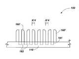
- the second spacers 160 ′may have a width of about x/3 and may be separated from one another by a distance of about x/3.
- FIG. 10also illustrates the initial width x of the resist layer 140 ′ and the original space B between neighboring portions of the resist layer 140 ′.
- second spacers 160 ′having about one-third the width of the resist layer 140 ′ may be formed on target layer 110 .
- About equal spacingmay be achieved between the adjacent second spacers 160 ′.
- the target layer 110may be patterned as shown by broken line 161 , forming features 163 having a CD about 1 ⁇ 3 of the CD of the resist layer 140 ′.
- Target layer 110may be patterned by conventional techniques, which are not described in detail herein.
- additional spacer etch processesmay be used. For instance, a third (or additional) spacers may be formed over the second spacers 160 ′ after removing the intermediate layer 120 ′.
- the additional spacersmay have a thickness about equal to the CD of the features to be formed on the target layer 110 .
- the additional spacersmay be deposited at a thickness that corresponds to a fraction of x.
- the target layer 110may be utilized in semiconductor devices, such as dynamic random access memories (DRAMs), static random access memories (SRAMs), ferroelectric memories (FE), NAND and NOR Flash memories, microprocessors, such as with field-effect transistors (FETs), and flat-panel displays.
- the target layer 110may be a wafer substrate to be etched for the formation of shallow trench isolation (STI) structures isolating cells of a NAND flash device.
- Target layer 110may also be a conductive active layer, such as a polysilicon layer to be patterned into gates for transistors.
- Target layer 110may also be a metal layer, such as aluminum, tungsten, titanium, or copper, to be patterned as conductive lines connecting different active areas.
- materialmay be deposited on target layer 110 filling in voids between the second spacers 160 ′.
- any of the above actsmay be combined with other acts depending upon the materials used in the different layers and the processes used in forming and removing the materials. Additionally, any of the above acts may utilize multiple processes to accomplish the single act. After any act, further processing, not described above, may also occur. Examples of additional processing include ion implantation, diffusion doping, deposition of additional layers, wet or dry etching, and chemical-mechanical polishing. For the sake of example only, after any act, etching may be used to narrow, smooth, or improve the profile of an exposed layer.
- a 248 nm photoresist materialin combination with two or more spacer etch processes, may be used to form small features on the target layer 110 .
- the featuresmay have a CD that is a fraction of the CD conventionally achievable with the 248 nm photoresist.
- 248 nm photolithographymay be used to pattern the resist layer 140 at a resolution within the limits of this technique. As this stage, the remaining portions of the resist layer 140 ′ may have larger CDs than the CDs of the features to be formed in the target layer 110 .
- the spacer etch processesmay be conducted to form features having CDs one-third or one-fourth of the CDs of the portions of the resist layer 140 ′.
- the CDs of the featuresmay be smaller than those achievable using a more advanced photolithography technique, such as 193 nm photolithography.
- the above-described embodimentsmay be utilized to produce a reduced CD, or pitch, of the features on the target layer 110 relative to the CD of etched portions of the resist layer 140 ′.
- xwhen resist layer 140 ′, as illustrated in FIG. 2 , is formed using a 248 nm photoresist, x may be about 120 nm and B may be about 120 nm, for a total pitch of about 240 nm.
- the width of second spacers 160 ′as illustrated in FIG. 10 , may be about 40 nm and the distance between neighboring second spacers 160 ′ may also equal about 40 nm, for a total pitch of about 80 nm.
- the width of the resist layer 140 ′may be any width within a range of from about 30 nm to about 150 nm.
- features having a width of from about 10 nm to about 50 nmmay be formed in the target layer 110 .
- Embodiments of the inventionalso encompass a method of reducing the CD or minimum pitch of a feature by a factor of 4.
- An embodiment of a quadruple pitch reduction method according to the present inventionis illustrated in FIGS. 11-19 .
- Substantially similar materials and processing actsare used in this embodiment relative to the previous embodiment.
- the embodiment illustrated in FIGS. 11-19differs from the embodiment illustrated in FIGS. 1-10 , inter alia, in that the width of the resist layer 140 ′ is different, as is the spacing between adjacent portions of the resist layer 140 ′.
- the thicknesses of the deposited spacer layersdiffer.
- FIG. 11illustrates substantially the same partially fabricated integrated circuit device 100 illustrated in FIG. 2 , except that the remaining portions of the resist layer 140 ′ have a width of about 3x/4 and the spacing between adjacent portions of the resist layer 140 ′ is about 5x/4.
- the resist layer 140may be deposited and patterned as known in the art, to produce this spacing. For the sake of example only, the resist layer 140 may be patterned such that portions of the resist layer 140 ′ have a width of about x and the spacing between adjacent portions of the resist layer 140 ′ is about x.
- the portions of the resist layer 140 ′may be further etched or trimmed to have a width of about 3x/4, which increases the spacing between adjacent portions of the resist layer 140 ′ to about 5x/4.
- FIG. 12illustrates that the first spacer layer 150 may be formed over the resist layer 140 ′ and the anti-reflective layer 130 .
- the first spacer layer 150may be conformally deposited at a thickness of about x/4. As previously described, the thickness of the first spacer layer 150 may correspond to the CD of the features to be formed on the target layer 110 .
- the first spacer layer 150may be deposited by ALD.
- FIG. 13illustrates the removal of the first spacer layer 150 from substantially horizontal surfaces of the resist layer 140 ′ and the anti-reflective layer 130 , such as by an anisotropic etch.
- the first spacer material 150may remain on substantially vertical surfaces of the resist layer 140 ′, forming the first spacers 150 ′.
- the first spacers 150 ′may have a thickness equal to about x/4 and the spacing between adjacent portions of the resist layer 140 ′ may be reduced to about 3x/4.
- FIG. 14illustrates that the resist layer 140 ′ may be removed, leaving the first spacers 150 ′ on top of anti-reflective layer 130 .
- the spacing between adjacent first spacers 150 ′may be about 3x/4.
- FIG. 15illustrates that portions of anti-reflective layer 130 and intermediate layer 120 may be removed using the first spacers 150 ′ as a mask. As such, the portions of the anti-reflective layer 130 ′ and the intermediate layer 120 ′ beneath the first spacers 150 ′ may be protected during this etch.
- FIG. 16illustrates that the first spacers 150 ′ and the anti-reflective layer 130 ′ may be removed, leaving the intermediate layer 120 ′ on the surface of target layer 110 .
- the intermediate layer 120 ′may have a width of about x/4 and the distance between adjacent portions of the intermediate layer 120 ′ may be about 3x/4.
- FIG. 17illustrates that the second spacer layer 160 may be formed on portions of the intermediate layer 120 ′.
- the second spacer layer 160may be conformally deposited, such as by ALD, at a thickness of about x/4.
- FIG. 18illustrates that substantially horizontal portions of the second spacer layer 160 may be removed, exposing the top surfaces of the intermediate layer 120 ′ and portions of the target layer 110 .
- the remaining portions of the second spacer layer 160may form the second spacers 160 ′.
- the intermediate layer 120 ′may be removed, as illustrated in FIG. 19 .
- the second spacers 160 ′may have a width of about x/4 and may be separated from adjacent second spacers 160 ′ by a distance of about x/4.
- the spacing between the adjacent second spacers 160 ′may enable features having one-fourth the CD of the resist layer 140 ′ to be formed on the target layer 110 .
- the target layer 110may be patterned as shown by broken line 161 , forming features 163 having the desired quadruple reduction in pitch.
- the resulting width of the second spacers 160 ′may be about 30 nm and the distance between adjacent second spacers 160 ′ may also be equal to about 30 nm.
- features having a CD about one-fourth of the CD of the resist layer 140 ′may be formed.
- embodiments of the present inventionmay be utilized to produce features in a target layer 110 having a CD about one-third or one-fourth the CD of the width of the resist layer 140 ′.
- features having a CD less than about 50 nmmay be formed in the target layer 110 .
- the thickness of the first and second spacer layers 150 , 160may be precisely controlled by ALD, the CDs of the features formed in the target layer 110 may be precisely controlled.
Landscapes
- Engineering & Computer Science (AREA)
- Physics & Mathematics (AREA)
- Condensed Matter Physics & Semiconductors (AREA)
- General Physics & Mathematics (AREA)
- Manufacturing & Machinery (AREA)
- Computer Hardware Design (AREA)
- Microelectronics & Electronic Packaging (AREA)
- Power Engineering (AREA)
- Chemical & Material Sciences (AREA)
- Inorganic Chemistry (AREA)
- Internal Circuitry In Semiconductor Integrated Circuit Devices (AREA)
- Drying Of Semiconductors (AREA)
- Electrodes Of Semiconductors (AREA)
- Exposure Of Semiconductors, Excluding Electron Or Ion Beam Exposure (AREA)
- Photosensitive Polymer And Photoresist Processing (AREA)
- Semiconductor Memories (AREA)
Abstract
Description
Claims (12)
Priority Applications (9)
| Application Number | Priority Date | Filing Date | Title |
|---|---|---|---|
| US11/606,613US7807575B2 (en) | 2006-11-29 | 2006-11-29 | Methods to reduce the critical dimension of semiconductor devices |
| CN2007800439106ACN101542685B (en) | 2006-11-29 | 2007-11-21 | Methods to reduce the critical dimension of semiconductor devices and partially fabricated semiconductor devices having reduced critical dimensions |
| PCT/US2007/085371WO2008067228A1 (en) | 2006-11-29 | 2007-11-21 | Methods to reduce the critical dimension of semiconductor devices and partially fabricated semiconductor devices having reduced critical dimensions |
| JP2009539423AJP5532303B2 (en) | 2006-11-29 | 2007-11-21 | Method for reducing critical dimensions of semiconductor devices |
| EP07864709.6AEP2095402B1 (en) | 2006-11-29 | 2007-11-21 | Methods to reduce the critical dimension of semiconductor devices and partially fabricated semiconductor devices having reduced critical dimensions |
| KR1020097011807AKR101091298B1 (en) | 2006-11-29 | 2007-11-21 | Methods to reduce the critical dimension of semiconductor devices and partially fabricated semiconductor devices having reduced critical dimensions |
| TW096145471ATWI356446B (en) | 2006-11-29 | 2007-11-29 | Methods to reduce the critical dimension of semico |
| US12/887,906US8338304B2 (en) | 2006-11-29 | 2010-09-22 | Methods to reduce the critical dimension of semiconductor devices and related semiconductor devices |
| US13/619,905US8836083B2 (en) | 2006-11-29 | 2012-09-14 | Methods to reduce the critical dimension of semiconductor devices and related semiconductor devices |
Applications Claiming Priority (1)
| Application Number | Priority Date | Filing Date | Title |
|---|---|---|---|
| US11/606,613US7807575B2 (en) | 2006-11-29 | 2006-11-29 | Methods to reduce the critical dimension of semiconductor devices |
Related Child Applications (1)
| Application Number | Title | Priority Date | Filing Date |
|---|---|---|---|
| US12/887,906DivisionUS8338304B2 (en) | 2006-11-29 | 2010-09-22 | Methods to reduce the critical dimension of semiconductor devices and related semiconductor devices |
Publications (2)
| Publication Number | Publication Date |
|---|---|
| US20080122125A1 US20080122125A1 (en) | 2008-05-29 |
| US7807575B2true US7807575B2 (en) | 2010-10-05 |
Family
ID=39273348
Family Applications (3)
| Application Number | Title | Priority Date | Filing Date |
|---|---|---|---|
| US11/606,613Active2028-01-31US7807575B2 (en) | 2006-11-29 | 2006-11-29 | Methods to reduce the critical dimension of semiconductor devices |
| US12/887,906ActiveUS8338304B2 (en) | 2006-11-29 | 2010-09-22 | Methods to reduce the critical dimension of semiconductor devices and related semiconductor devices |
| US13/619,905Active2027-06-02US8836083B2 (en) | 2006-11-29 | 2012-09-14 | Methods to reduce the critical dimension of semiconductor devices and related semiconductor devices |
Family Applications After (2)
| Application Number | Title | Priority Date | Filing Date |
|---|---|---|---|
| US12/887,906ActiveUS8338304B2 (en) | 2006-11-29 | 2010-09-22 | Methods to reduce the critical dimension of semiconductor devices and related semiconductor devices |
| US13/619,905Active2027-06-02US8836083B2 (en) | 2006-11-29 | 2012-09-14 | Methods to reduce the critical dimension of semiconductor devices and related semiconductor devices |
Country Status (7)
| Country | Link |
|---|---|
| US (3) | US7807575B2 (en) |
| EP (1) | EP2095402B1 (en) |
| JP (1) | JP5532303B2 (en) |
| KR (1) | KR101091298B1 (en) |
| CN (1) | CN101542685B (en) |
| TW (1) | TWI356446B (en) |
| WO (1) | WO2008067228A1 (en) |
Cited By (30)
| Publication number | Priority date | Publication date | Assignee | Title |
|---|---|---|---|---|
| US20090061641A1 (en)* | 2007-09-03 | 2009-03-05 | Hynix Semiconductor Inc. | Method of forming a micro pattern of a semiconductor device |
| US20110006402A1 (en)* | 2006-11-29 | 2011-01-13 | Micron Technology, Inc. | Methods to reduce the critical dimension of semiconductor devices and related semiconductor devices |
| US20110127582A1 (en)* | 2009-12-01 | 2011-06-02 | International Business Machines Corporation | Multiplying pattern density by single sidewall imaging transfer |
| US8114724B2 (en)* | 2010-06-10 | 2012-02-14 | Hynix Semiconductor Inc. | Method for fabricating semiconductor device |
| US20120049377A1 (en)* | 2010-09-01 | 2012-03-01 | Yang Song-Yi | Semiconductor device and method of double photolithography process for forming patterns of the semiconductor device |
| US8389383B1 (en) | 2011-04-05 | 2013-03-05 | Micron Technology, Inc. | Patterned semiconductor bases, and patterning methods |
| US20130309854A1 (en)* | 2012-05-16 | 2013-11-21 | Commissariat A L'energie Atomique Et Aux Energies Alternatives | Method for manufacturing a substrate provided with different active areas and with planar and three-dimensional transistors |
| US8703570B2 (en) | 2008-12-04 | 2014-04-22 | Micron Technology, Inc. | Methods of fabricating substrates |
| US8735296B2 (en)* | 2012-07-18 | 2014-05-27 | International Business Machines Corporation | Method of simultaneously forming multiple structures having different critical dimensions using sidewall transfer |
| US8796155B2 (en) | 2008-12-04 | 2014-08-05 | Micron Technology, Inc. | Methods of fabricating substrates |
| US8846517B2 (en) | 2012-07-06 | 2014-09-30 | Micron Technology, Inc. | Methods of forming a pattern on a substrate |
| US8852851B2 (en) | 2006-07-10 | 2014-10-07 | Micron Technology, Inc. | Pitch reduction technology using alternating spacer depositions during the formation of a semiconductor device and systems including same |
| US8889561B2 (en)* | 2012-12-10 | 2014-11-18 | Globalfoundries Inc. | Double sidewall image transfer process |
| US8901700B2 (en) | 2008-05-05 | 2014-12-02 | Micron Technology, Inc. | Semiconductor structures |
| US8969215B2 (en) | 2012-11-20 | 2015-03-03 | Samsung Electronics Co., Ltd. | Methods of fabricating semiconductor devices using double patterning technology |
| US20150155171A1 (en)* | 2013-12-04 | 2015-06-04 | Taiwan Semiconductor Manufacturing Company, Ltd. | Lithography Using High Selectivity Spacers for Pitch Reduction |
| US9105295B2 (en) | 2013-02-25 | 2015-08-11 | HGST Netherlands B.V. | Pattern tone reversal |
| US9153458B2 (en) | 2011-05-05 | 2015-10-06 | Micron Technology, Inc. | Methods of forming a pattern on a substrate |
| US9177794B2 (en) | 2012-01-13 | 2015-11-03 | Micron Technology, Inc. | Methods of patterning substrates |
| US9330934B2 (en) | 2009-05-18 | 2016-05-03 | Micron Technology, Inc. | Methods of forming patterns on substrates |
| US9378979B2 (en) | 2012-11-20 | 2016-06-28 | Samsung Electronics Co., Ltd. | Methods of fabricating semiconductor devices and devices fabricated thereby |
| US9646983B2 (en) | 2014-12-19 | 2017-05-09 | Samsung Electronics Co., Ltd. | Semiconductor device and method of manufacturing the same |
| US9852917B2 (en)* | 2016-03-22 | 2017-12-26 | International Business Machines Corporation | Methods of fabricating semiconductor fins by double sidewall image transfer patterning through localized oxidation enhancement of sacrificial mandrel sidewalls |
| US9882028B2 (en)* | 2016-06-29 | 2018-01-30 | International Business Machines Corporation | Pitch split patterning for semiconductor devices |
| US9911828B2 (en) | 2015-01-29 | 2018-03-06 | Samsung Electronics Co., Ltd. | Methods of fabricating a semiconductor device |
| US9985025B1 (en) | 2016-11-24 | 2018-05-29 | Samsung Electronics Co., Ltd. | Active pattern structure and semiconductor device including the same |
| US10151981B2 (en) | 2008-05-22 | 2018-12-11 | Micron Technology, Inc. | Methods of forming structures supported by semiconductor substrates |
| US20190019676A1 (en)* | 2017-07-15 | 2019-01-17 | Micromaterials Llc | Mask Scheme For Cut Pattern Flow With Enlarged EPE Window |
| US11024511B1 (en) | 2020-04-21 | 2021-06-01 | Winbond Electronics Corp. | Patterning method |
| US20230402277A1 (en)* | 2022-06-12 | 2023-12-14 | Taiwan Semiconductor Manufacturing Company, Ltd. | Semiconductor structure and manufacturing method thereof |
Families Citing this family (476)
| Publication number | Priority date | Publication date | Assignee | Title |
|---|---|---|---|---|
| US9460924B2 (en)* | 2007-03-26 | 2016-10-04 | GlobalFoundries, Inc. | Semiconductor device having structure with fractional dimension of the minimum dimension of a lithography system |
| US7939451B2 (en)* | 2007-06-07 | 2011-05-10 | Macronix International Co., Ltd. | Method for fabricating a pattern |
| US8143156B2 (en)* | 2007-06-20 | 2012-03-27 | Sandisk Technologies Inc. | Methods of forming high density semiconductor devices using recursive spacer technique |
| CN101345190B (en)* | 2007-07-10 | 2012-05-23 | 旺宏电子股份有限公司 | pattern forming method |
| US8980756B2 (en) | 2007-07-30 | 2015-03-17 | Micron Technology, Inc. | Methods for device fabrication using pitch reduction |
| US8357618B2 (en)* | 2007-10-26 | 2013-01-22 | Applied Materials, Inc. | Frequency doubling using a photo-resist template mask |
| US8329385B2 (en)* | 2008-06-10 | 2012-12-11 | Kabushiki Kaisha Toshiba | Method of manufacturing a semiconductor device |
| JP5224919B2 (en)* | 2008-06-10 | 2013-07-03 | 株式会社東芝 | Manufacturing method of semiconductor device |
| US20090311634A1 (en)* | 2008-06-11 | 2009-12-17 | Tokyo Electron Limited | Method of double patterning using sacrificial structure |
| JP5336283B2 (en)* | 2008-09-03 | 2013-11-06 | 信越化学工業株式会社 | Pattern formation method |
| US10378106B2 (en) | 2008-11-14 | 2019-08-13 | Asm Ip Holding B.V. | Method of forming insulation film by modified PEALD |
| US8273634B2 (en)* | 2008-12-04 | 2012-09-25 | Micron Technology, Inc. | Methods of fabricating substrates |
| US20100183957A1 (en)* | 2009-01-21 | 2010-07-22 | Seagate Technology Llc | Method of Patterned Media Template Formation and Templates |
| US8268543B2 (en)* | 2009-03-23 | 2012-09-18 | Micron Technology, Inc. | Methods of forming patterns on substrates |
| US9394608B2 (en) | 2009-04-06 | 2016-07-19 | Asm America, Inc. | Semiconductor processing reactor and components thereof |
| JP5425514B2 (en)* | 2009-04-16 | 2014-02-26 | AzエレクトロニックマテリアルズIp株式会社 | Fine pattern forming method |
| US8802201B2 (en) | 2009-08-14 | 2014-08-12 | Asm America, Inc. | Systems and methods for thin-film deposition of metal oxides using excited nitrogen-oxygen species |
| US8455364B2 (en)* | 2009-11-06 | 2013-06-04 | International Business Machines Corporation | Sidewall image transfer using the lithographic stack as the mandrel |
| JP5574679B2 (en)* | 2009-11-17 | 2014-08-20 | 株式会社東芝 | Manufacturing method of semiconductor device |
| US20110129991A1 (en)* | 2009-12-02 | 2011-06-02 | Kyle Armstrong | Methods Of Patterning Materials, And Methods Of Forming Memory Cells |
| JP5391055B2 (en)* | 2009-12-25 | 2014-01-15 | 東京エレクトロン株式会社 | Semiconductor device manufacturing method and semiconductor device manufacturing system |
| TWI412487B (en)* | 2009-12-31 | 2013-10-21 | Huang Chung Cheng | Method of forming nanowire structure |
| JP2011233878A (en)* | 2010-04-09 | 2011-11-17 | Elpida Memory Inc | Method for manufacturing semiconductor device |
| US20110294075A1 (en)* | 2010-05-25 | 2011-12-01 | United Microelectronics Corp. | Patterning method |
| US8518788B2 (en) | 2010-08-11 | 2013-08-27 | Micron Technology, Inc. | Methods of forming a plurality of capacitors |
| US8455341B2 (en) | 2010-09-02 | 2013-06-04 | Micron Technology, Inc. | Methods of forming features of integrated circuitry |
| US20120085733A1 (en)* | 2010-10-07 | 2012-04-12 | Applied Materials, Inc. | Self aligned triple patterning |
| CN102064096B (en)* | 2010-12-03 | 2012-07-25 | 北京大学 | Preparation method of hair line |
| KR101225601B1 (en)* | 2010-12-16 | 2013-01-24 | 한국과학기술원 | Fabrication method of large area nanoscale pattern |
| US8314034B2 (en)* | 2010-12-23 | 2012-11-20 | Intel Corporation | Feature size reduction |
| US8901016B2 (en) | 2010-12-28 | 2014-12-02 | Asm Japan K.K. | Method of forming metal oxide hardmask |
| KR20120077505A (en) | 2010-12-30 | 2012-07-10 | 삼성전자주식회사 | Nonvolatile semiconductor memory device and the method of fabricating the same |
| US20120175745A1 (en)* | 2011-01-06 | 2012-07-12 | Nanya Technology Corporation | Methods for fabricating semiconductor devices and semiconductor devices using the same |
| JP5473962B2 (en)* | 2011-02-22 | 2014-04-16 | 東京エレクトロン株式会社 | Pattern forming method and semiconductor device manufacturing method |
| TWI484534B (en)* | 2011-03-09 | 2015-05-11 | Winbond Electronics Corp | Method for reducing pitch |
| JP5330440B2 (en)* | 2011-03-23 | 2013-10-30 | 株式会社東芝 | Manufacturing method of semiconductor device |
| JP5395837B2 (en) | 2011-03-24 | 2014-01-22 | 株式会社東芝 | Manufacturing method of semiconductor device |
| US20120280354A1 (en)* | 2011-05-05 | 2012-11-08 | Synopsys, Inc. | Methods for fabricating high-density integrated circuit devices |
| US9312155B2 (en) | 2011-06-06 | 2016-04-12 | Asm Japan K.K. | High-throughput semiconductor-processing apparatus equipped with multiple dual-chamber modules |
| US9793148B2 (en) | 2011-06-22 | 2017-10-17 | Asm Japan K.K. | Method for positioning wafers in multiple wafer transport |
| US10364496B2 (en) | 2011-06-27 | 2019-07-30 | Asm Ip Holding B.V. | Dual section module having shared and unshared mass flow controllers |
| US10854498B2 (en) | 2011-07-15 | 2020-12-01 | Asm Ip Holding B.V. | Wafer-supporting device and method for producing same |
| US20130023129A1 (en) | 2011-07-20 | 2013-01-24 | Asm America, Inc. | Pressure transmitter for a semiconductor processing environment |
| US8809169B2 (en)* | 2011-09-30 | 2014-08-19 | Tokyo Electron Limited | Multi-layer pattern for alternate ALD processes |
| US9076680B2 (en) | 2011-10-18 | 2015-07-07 | Micron Technology, Inc. | Integrated circuitry, methods of forming capacitors, and methods of forming integrated circuitry comprising an array of capacitors and circuitry peripheral to the array |
| US9017481B1 (en) | 2011-10-28 | 2015-04-28 | Asm America, Inc. | Process feed management for semiconductor substrate processing |
| CN104025256B (en)* | 2011-12-29 | 2017-03-29 | 英特尔公司 | Double patterning photoetching technique |
| TWI510854B (en)* | 2011-12-31 | 2015-12-01 | 羅門哈斯電子材料有限公司 | Photoresist pattern trimming methods |
| JP6108832B2 (en)* | 2011-12-31 | 2017-04-05 | ローム アンド ハース エレクトロニック マテリアルズ エルエルシーRohm and Haas Electronic Materials LLC | Photoresist pattern trimming method |
| CN103367108B (en)* | 2012-03-31 | 2015-10-14 | 中芯国际集成电路制造(上海)有限公司 | The pattern of the two patterning process of autoregistration and formation thereof |
| CN103367156B (en)* | 2012-03-31 | 2015-10-14 | 中芯国际集成电路制造(上海)有限公司 | The formation method of semiconductor device, the formation method of fin field effect pipe |
| US8946830B2 (en) | 2012-04-04 | 2015-02-03 | Asm Ip Holdings B.V. | Metal oxide protective layer for a semiconductor device |
| US8524605B1 (en)* | 2012-04-16 | 2013-09-03 | Vigma Nanoelectronics | Fabrication and mask design methods using spatial frequency sextupling technique |
| US9005877B2 (en)* | 2012-05-15 | 2015-04-14 | Tokyo Electron Limited | Method of forming patterns using block copolymers and articles thereof |
| US9349595B2 (en)* | 2012-07-11 | 2016-05-24 | Taiwan Semiconductor Manufacturing Company, Ltd. | Methods of manufacturing semiconductor devices |
| US9558931B2 (en) | 2012-07-27 | 2017-01-31 | Asm Ip Holding B.V. | System and method for gas-phase sulfur passivation of a semiconductor surface |
| US9449839B2 (en) | 2012-08-06 | 2016-09-20 | Taiwan Semiconductor Manufacturing Co., Ltd. | Self-assembled monolayer for pattern formation |
| US8883646B2 (en)* | 2012-08-06 | 2014-11-11 | Taiwan Semiconductor Manufacturing Co., Ltd. | Self-assembled monolayer for pattern formation |
| US9659799B2 (en) | 2012-08-28 | 2017-05-23 | Asm Ip Holding B.V. | Systems and methods for dynamic semiconductor process scheduling |
| CN103632928A (en)* | 2012-08-29 | 2014-03-12 | 中芯国际集成电路制造(上海)有限公司 | Self-aligned double patterning formation method |
| US9021985B2 (en) | 2012-09-12 | 2015-05-05 | Asm Ip Holdings B.V. | Process gas management for an inductively-coupled plasma deposition reactor |
| US9324811B2 (en) | 2012-09-26 | 2016-04-26 | Asm Ip Holding B.V. | Structures and devices including a tensile-stressed silicon arsenic layer and methods of forming same |
| JP5829994B2 (en)* | 2012-10-01 | 2015-12-09 | 信越化学工業株式会社 | Pattern formation method |
| US10714315B2 (en) | 2012-10-12 | 2020-07-14 | Asm Ip Holdings B.V. | Semiconductor reaction chamber showerhead |
| CN103904018B (en)* | 2012-12-24 | 2017-08-01 | 中芯国际集成电路制造(上海)有限公司 | A kind of manufacture method of semiconductor devices |
| US9640416B2 (en) | 2012-12-26 | 2017-05-02 | Asm Ip Holding B.V. | Single-and dual-chamber module-attachable wafer-handling chamber |
| US20160376700A1 (en) | 2013-02-01 | 2016-12-29 | Asm Ip Holding B.V. | System for treatment of deposition reactor |
| US9484191B2 (en) | 2013-03-08 | 2016-11-01 | Asm Ip Holding B.V. | Pulsed remote plasma method and system |
| US9589770B2 (en) | 2013-03-08 | 2017-03-07 | Asm Ip Holding B.V. | Method and systems for in-situ formation of intermediate reactive species |
| US9153478B2 (en) | 2013-03-15 | 2015-10-06 | Taiwan Semiconductor Manufacturing Company, Ltd. | Spacer etching process for integrated circuit design |
| US9721784B2 (en)* | 2013-03-15 | 2017-08-01 | Applied Materials, Inc. | Ultra-conformal carbon film deposition |
| US8975187B2 (en)* | 2013-03-15 | 2015-03-10 | Taiwan Semiconductor Manufacturing Company, Ltd. | Stress-controlled formation of tin hard mask |
| CN104103574B (en)* | 2013-04-10 | 2017-12-29 | 中芯国际集成电路制造(上海)有限公司 | The preparation method of semiconductor devices |
| KR20140137734A (en)* | 2013-05-23 | 2014-12-03 | 삼성디스플레이 주식회사 | Method of manufacturing reflective polarizer plate and method fo manufacturing in-cell reflective polarizer plate |
| CN103325709B (en)* | 2013-05-28 | 2016-08-10 | 上海华力微电子有限公司 | A kind of no-nitrogen medium reflecting resistant layer off-line detecting |
| US9437443B2 (en) | 2013-06-12 | 2016-09-06 | Globalfoundries Inc. | Low-temperature sidewall image transfer process using ALD metals, metal oxides and metal nitrides |
| US8993054B2 (en) | 2013-07-12 | 2015-03-31 | Asm Ip Holding B.V. | Method and system to reduce outgassing in a reaction chamber |
| US9018111B2 (en) | 2013-07-22 | 2015-04-28 | Asm Ip Holding B.V. | Semiconductor reaction chamber with plasma capabilities |
| US9793115B2 (en) | 2013-08-14 | 2017-10-17 | Asm Ip Holding B.V. | Structures and devices including germanium-tin films and methods of forming same |
| US9165770B2 (en)* | 2013-09-26 | 2015-10-20 | GlobalFoundries, Inc. | Methods for fabricating integrated circuits using improved masks |
| US9240412B2 (en) | 2013-09-27 | 2016-01-19 | Asm Ip Holding B.V. | Semiconductor structure and device and methods of forming same using selective epitaxial process |
| US9123772B2 (en)* | 2013-10-02 | 2015-09-01 | GlobalFoundries, Inc. | FinFET fabrication method |
| US9556516B2 (en) | 2013-10-09 | 2017-01-31 | ASM IP Holding B.V | Method for forming Ti-containing film by PEALD using TDMAT or TDEAT |
| US8975129B1 (en)* | 2013-11-13 | 2015-03-10 | Taiwan Semiconductor Manufacturing Company, Ltd. | Method of making a FinFET device |
| US9070630B2 (en)* | 2013-11-26 | 2015-06-30 | Taiwan Semiconductor Manufacturing Company, Ltd. | Mechanisms for forming patterns |
| US10179947B2 (en) | 2013-11-26 | 2019-01-15 | Asm Ip Holding B.V. | Method for forming conformal nitrided, oxidized, or carbonized dielectric film by atomic layer deposition |
| KR102114965B1 (en)* | 2014-02-07 | 2020-05-26 | 삼성디스플레이 주식회사 | Manufacturing method of reflective polarizer plate and display device having reflective polarizer plate |
| US10683571B2 (en) | 2014-02-25 | 2020-06-16 | Asm Ip Holding B.V. | Gas supply manifold and method of supplying gases to chamber using same |
| KR102223035B1 (en) | 2014-03-05 | 2021-03-04 | 삼성전자주식회사 | Method of forming patterns for semiconductor device |
| US9447498B2 (en) | 2014-03-18 | 2016-09-20 | Asm Ip Holding B.V. | Method for performing uniform processing in gas system-sharing multiple reaction chambers |
| US10167557B2 (en) | 2014-03-18 | 2019-01-01 | Asm Ip Holding B.V. | Gas distribution system, reactor including the system, and methods of using the same |
| US11015245B2 (en) | 2014-03-19 | 2021-05-25 | Asm Ip Holding B.V. | Gas-phase reactor and system having exhaust plenum and components thereof |
| CN103903972A (en)* | 2014-04-22 | 2014-07-02 | 上海华力微电子有限公司 | Manufacturing method of graphs with small size |
| US9404587B2 (en) | 2014-04-24 | 2016-08-02 | ASM IP Holding B.V | Lockout tagout for semiconductor vacuum valve |
| US9548201B2 (en)* | 2014-06-20 | 2017-01-17 | Applied Materials, Inc. | Self-aligned multiple spacer patterning schemes for advanced nanometer technology |
| JP5869057B2 (en)* | 2014-06-30 | 2016-02-24 | ウィンボンド エレクトロニクス コーポレーション | Semiconductor memory device |
| US10858737B2 (en) | 2014-07-28 | 2020-12-08 | Asm Ip Holding B.V. | Showerhead assembly and components thereof |
| US9543180B2 (en) | 2014-08-01 | 2017-01-10 | Asm Ip Holding B.V. | Apparatus and method for transporting wafers between wafer carrier and process tool under vacuum |
| US9890456B2 (en) | 2014-08-21 | 2018-02-13 | Asm Ip Holding B.V. | Method and system for in situ formation of gas-phase compounds |
| US10941490B2 (en) | 2014-10-07 | 2021-03-09 | Asm Ip Holding B.V. | Multiple temperature range susceptor, assembly, reactor and system including the susceptor, and methods of using the same |
| JP6366454B2 (en)* | 2014-10-07 | 2018-08-01 | 東京エレクトロン株式会社 | Method for processing an object |
| US9657845B2 (en) | 2014-10-07 | 2017-05-23 | Asm Ip Holding B.V. | Variable conductance gas distribution apparatus and method |
| US9685332B2 (en)* | 2014-10-17 | 2017-06-20 | Taiwan Semiconductor Manufacturing Company, Ltd. | Iterative self-aligned patterning |
| KR102300403B1 (en) | 2014-11-19 | 2021-09-09 | 에이에스엠 아이피 홀딩 비.브이. | Method of depositing thin film |
| KR102263121B1 (en) | 2014-12-22 | 2021-06-09 | 에이에스엠 아이피 홀딩 비.브이. | Semiconductor device and manufacuring method thereof |
| US9754785B2 (en) | 2015-01-14 | 2017-09-05 | Samsung Electronics Co., Ltd. | Methods of manufacturing semiconductor devices |
| KR102327667B1 (en)* | 2015-01-14 | 2021-11-17 | 삼성전자주식회사 | Methods of manufacturing semiconductor devices |
| JP6559430B2 (en)* | 2015-01-30 | 2019-08-14 | 東京エレクトロン株式会社 | Method for processing an object |
| US9673059B2 (en)* | 2015-02-02 | 2017-06-06 | Tokyo Electron Limited | Method for increasing pattern density in self-aligned patterning integration schemes |
| US9478415B2 (en) | 2015-02-13 | 2016-10-25 | Asm Ip Holding B.V. | Method for forming film having low resistance and shallow junction depth |
| US10529542B2 (en) | 2015-03-11 | 2020-01-07 | Asm Ip Holdings B.V. | Cross-flow reactor and method |
| US10276355B2 (en) | 2015-03-12 | 2019-04-30 | Asm Ip Holding B.V. | Multi-zone reactor, system including the reactor, and method of using the same |
| JP6462477B2 (en)* | 2015-04-27 | 2019-01-30 | 東京エレクトロン株式会社 | Method for processing an object |
| US9484202B1 (en)* | 2015-06-03 | 2016-11-01 | Applied Materials, Inc. | Apparatus and methods for spacer deposition and selective removal in an advanced patterning process |
| US9659771B2 (en) | 2015-06-11 | 2017-05-23 | Applied Materials, Inc. | Conformal strippable carbon film for line-edge-roughness reduction for advanced patterning |
| US10458018B2 (en) | 2015-06-26 | 2019-10-29 | Asm Ip Holding B.V. | Structures including metal carbide material, devices including the structures, and methods of forming same |
| US10600673B2 (en) | 2015-07-07 | 2020-03-24 | Asm Ip Holding B.V. | Magnetic susceptor to baseplate seal |
| US9899291B2 (en) | 2015-07-13 | 2018-02-20 | Asm Ip Holding B.V. | Method for protecting layer by forming hydrocarbon-based extremely thin film |
| US10043661B2 (en) | 2015-07-13 | 2018-08-07 | Asm Ip Holding B.V. | Method for protecting layer by forming hydrocarbon-based extremely thin film |
| US10083836B2 (en) | 2015-07-24 | 2018-09-25 | Asm Ip Holding B.V. | Formation of boron-doped titanium metal films with high work function |
| US10087525B2 (en) | 2015-08-04 | 2018-10-02 | Asm Ip Holding B.V. | Variable gap hard stop design |
| US9647114B2 (en) | 2015-08-14 | 2017-05-09 | Asm Ip Holding B.V. | Methods of forming highly p-type doped germanium tin films and structures and devices including the films |
| US9711345B2 (en) | 2015-08-25 | 2017-07-18 | Asm Ip Holding B.V. | Method for forming aluminum nitride-based film by PEALD |
| US9960072B2 (en) | 2015-09-29 | 2018-05-01 | Asm Ip Holding B.V. | Variable adjustment for precise matching of multiple chamber cavity housings |
| US9909214B2 (en) | 2015-10-15 | 2018-03-06 | Asm Ip Holding B.V. | Method for depositing dielectric film in trenches by PEALD |
| US10211308B2 (en) | 2015-10-21 | 2019-02-19 | Asm Ip Holding B.V. | NbMC layers |
| US10322384B2 (en) | 2015-11-09 | 2019-06-18 | Asm Ip Holding B.V. | Counter flow mixer for process chamber |
| US9455138B1 (en) | 2015-11-10 | 2016-09-27 | Asm Ip Holding B.V. | Method for forming dielectric film in trenches by PEALD using H-containing gas |
| US9905420B2 (en) | 2015-12-01 | 2018-02-27 | Asm Ip Holding B.V. | Methods of forming silicon germanium tin films and structures and devices including the films |
| US9576817B1 (en)* | 2015-12-03 | 2017-02-21 | International Business Machines Corporation | Pattern decomposition for directed self assembly patterns templated by sidewall image transfer |
| US9620380B1 (en)* | 2015-12-17 | 2017-04-11 | GlobalFoundries, Inc. | Methods for fabricating integrated circuits using self-aligned quadruple patterning |
| KR102449195B1 (en) | 2015-12-18 | 2022-09-29 | 삼성전자주식회사 | Semiconductor device and method for manufacturing the semiconductor device |
| US9607837B1 (en) | 2015-12-21 | 2017-03-28 | Asm Ip Holding B.V. | Method for forming silicon oxide cap layer for solid state diffusion process |
| US9735024B2 (en) | 2015-12-28 | 2017-08-15 | Asm Ip Holding B.V. | Method of atomic layer etching using functional group-containing fluorocarbon |
| US9627221B1 (en) | 2015-12-28 | 2017-04-18 | Asm Ip Holding B.V. | Continuous process incorporating atomic layer etching |
| US11139308B2 (en) | 2015-12-29 | 2021-10-05 | Asm Ip Holding B.V. | Atomic layer deposition of III-V compounds to form V-NAND devices |
| US10157742B2 (en) | 2015-12-31 | 2018-12-18 | Taiwan Semiconductor Manufacturing Co., Ltd. | Method for mandrel and spacer patterning |
| KR102398664B1 (en)* | 2016-01-26 | 2022-05-16 | 삼성전자주식회사 | Method of manufacturing semiconductor device |
| US9754779B1 (en) | 2016-02-19 | 2017-09-05 | Asm Ip Holding B.V. | Method for forming silicon nitride film selectively on sidewalls or flat surfaces of trenches |
| US10529554B2 (en) | 2016-02-19 | 2020-01-07 | Asm Ip Holding B.V. | Method for forming silicon nitride film selectively on sidewalls or flat surfaces of trenches |
| US10468251B2 (en) | 2016-02-19 | 2019-11-05 | Asm Ip Holding B.V. | Method for forming spacers using silicon nitride film for spacer-defined multiple patterning |
| US10501866B2 (en) | 2016-03-09 | 2019-12-10 | Asm Ip Holding B.V. | Gas distribution apparatus for improved film uniformity in an epitaxial system |
| US10343920B2 (en) | 2016-03-18 | 2019-07-09 | Asm Ip Holding B.V. | Aligned carbon nanotubes |
| US9892913B2 (en) | 2016-03-24 | 2018-02-13 | Asm Ip Holding B.V. | Radial and thickness control via biased multi-port injection settings |
| US10190213B2 (en) | 2016-04-21 | 2019-01-29 | Asm Ip Holding B.V. | Deposition of metal borides |
| US10865475B2 (en) | 2016-04-21 | 2020-12-15 | Asm Ip Holding B.V. | Deposition of metal borides and silicides |
| US10087522B2 (en) | 2016-04-21 | 2018-10-02 | Asm Ip Holding B.V. | Deposition of metal borides |
| US10032628B2 (en) | 2016-05-02 | 2018-07-24 | Asm Ip Holding B.V. | Source/drain performance through conformal solid state doping |
| US10367080B2 (en) | 2016-05-02 | 2019-07-30 | Asm Ip Holding B.V. | Method of forming a germanium oxynitride film |
| KR102592471B1 (en) | 2016-05-17 | 2023-10-20 | 에이에스엠 아이피 홀딩 비.브이. | Method of forming metal interconnection and method of fabricating semiconductor device using the same |
| US11453943B2 (en) | 2016-05-25 | 2022-09-27 | Asm Ip Holding B.V. | Method for forming carbon-containing silicon/metal oxide or nitride film by ALD using silicon precursor and hydrocarbon precursor |
| US10388509B2 (en) | 2016-06-28 | 2019-08-20 | Asm Ip Holding B.V. | Formation of epitaxial layers via dislocation filtering |
| US10612137B2 (en) | 2016-07-08 | 2020-04-07 | Asm Ip Holdings B.V. | Organic reactants for atomic layer deposition |
| US9859151B1 (en) | 2016-07-08 | 2018-01-02 | Asm Ip Holding B.V. | Selective film deposition method to form air gaps |
| US9793135B1 (en) | 2016-07-14 | 2017-10-17 | ASM IP Holding B.V | Method of cyclic dry etching using etchant film |
| US10714385B2 (en) | 2016-07-19 | 2020-07-14 | Asm Ip Holding B.V. | Selective deposition of tungsten |
| KR102354490B1 (en) | 2016-07-27 | 2022-01-21 | 에이에스엠 아이피 홀딩 비.브이. | Method of processing a substrate |
| US9812320B1 (en) | 2016-07-28 | 2017-11-07 | Asm Ip Holding B.V. | Method and apparatus for filling a gap |
| US10395919B2 (en) | 2016-07-28 | 2019-08-27 | Asm Ip Holding B.V. | Method and apparatus for filling a gap |
| KR102532607B1 (en) | 2016-07-28 | 2023-05-15 | 에이에스엠 아이피 홀딩 비.브이. | Substrate processing apparatus and method of operating the same |
| US10177025B2 (en) | 2016-07-28 | 2019-01-08 | Asm Ip Holding B.V. | Method and apparatus for filling a gap |
| US9887082B1 (en) | 2016-07-28 | 2018-02-06 | Asm Ip Holding B.V. | Method and apparatus for filling a gap |
| US10090316B2 (en) | 2016-09-01 | 2018-10-02 | Asm Ip Holding B.V. | 3D stacked multilayer semiconductor memory using doped select transistor channel |
| US10410943B2 (en) | 2016-10-13 | 2019-09-10 | Asm Ip Holding B.V. | Method for passivating a surface of a semiconductor and related systems |
| CN107968046B (en)* | 2016-10-20 | 2020-09-04 | 中芯国际集成电路制造(上海)有限公司 | Method for manufacturing semiconductor device |
| US10643826B2 (en) | 2016-10-26 | 2020-05-05 | Asm Ip Holdings B.V. | Methods for thermally calibrating reaction chambers |
| US11532757B2 (en) | 2016-10-27 | 2022-12-20 | Asm Ip Holding B.V. | Deposition of charge trapping layers |
| US10643904B2 (en) | 2016-11-01 | 2020-05-05 | Asm Ip Holdings B.V. | Methods for forming a semiconductor device and related semiconductor device structures |
| US10714350B2 (en) | 2016-11-01 | 2020-07-14 | ASM IP Holdings, B.V. | Methods for forming a transition metal niobium nitride film on a substrate by atomic layer deposition and related semiconductor device structures |
| US10435790B2 (en) | 2016-11-01 | 2019-10-08 | Asm Ip Holding B.V. | Method of subatmospheric plasma-enhanced ALD using capacitively coupled electrodes with narrow gap |
| US10229833B2 (en) | 2016-11-01 | 2019-03-12 | Asm Ip Holding B.V. | Methods for forming a transition metal nitride film on a substrate by atomic layer deposition and related semiconductor device structures |
| US10134757B2 (en) | 2016-11-07 | 2018-11-20 | Asm Ip Holding B.V. | Method of processing a substrate and a device manufactured by using the method |
| KR102546317B1 (en) | 2016-11-15 | 2023-06-21 | 에이에스엠 아이피 홀딩 비.브이. | Gas supply unit and substrate processing apparatus including the same |
| US10340135B2 (en) | 2016-11-28 | 2019-07-02 | Asm Ip Holding B.V. | Method of topologically restricted plasma-enhanced cyclic deposition of silicon or metal nitride |
| KR102762543B1 (en) | 2016-12-14 | 2025-02-05 | 에이에스엠 아이피 홀딩 비.브이. | Substrate processing apparatus |
| US9916980B1 (en) | 2016-12-15 | 2018-03-13 | Asm Ip Holding B.V. | Method of forming a structure on a substrate |
| US11447861B2 (en) | 2016-12-15 | 2022-09-20 | Asm Ip Holding B.V. | Sequential infiltration synthesis apparatus and a method of forming a patterned structure |
| US11581186B2 (en) | 2016-12-15 | 2023-02-14 | Asm Ip Holding B.V. | Sequential infiltration synthesis apparatus |
| KR102700194B1 (en) | 2016-12-19 | 2024-08-28 | 에이에스엠 아이피 홀딩 비.브이. | Substrate processing apparatus |
| US10269558B2 (en) | 2016-12-22 | 2019-04-23 | Asm Ip Holding B.V. | Method of forming a structure on a substrate |
| US10867788B2 (en) | 2016-12-28 | 2020-12-15 | Asm Ip Holding B.V. | Method of forming a structure on a substrate |
| US11390950B2 (en) | 2017-01-10 | 2022-07-19 | Asm Ip Holding B.V. | Reactor system and method to reduce residue buildup during a film deposition process |
| US10655221B2 (en) | 2017-02-09 | 2020-05-19 | Asm Ip Holding B.V. | Method for depositing oxide film by thermal ALD and PEALD |
| US10468261B2 (en) | 2017-02-15 | 2019-11-05 | Asm Ip Holding B.V. | Methods for forming a metallic film on a substrate by cyclical deposition and related semiconductor device structures |
| US10529563B2 (en) | 2017-03-29 | 2020-01-07 | Asm Ip Holdings B.V. | Method for forming doped metal oxide films on a substrate by cyclical deposition and related semiconductor device structures |
| US10283353B2 (en) | 2017-03-29 | 2019-05-07 | Asm Ip Holding B.V. | Method of reforming insulating film deposited on substrate with recess pattern |
| US10103040B1 (en) | 2017-03-31 | 2018-10-16 | Asm Ip Holding B.V. | Apparatus and method for manufacturing a semiconductor device |
| USD830981S1 (en) | 2017-04-07 | 2018-10-16 | Asm Ip Holding B.V. | Susceptor for semiconductor substrate processing apparatus |
| KR102457289B1 (en) | 2017-04-25 | 2022-10-21 | 에이에스엠 아이피 홀딩 비.브이. | Method for depositing a thin film and manufacturing a semiconductor device |
| US10770286B2 (en) | 2017-05-08 | 2020-09-08 | Asm Ip Holdings B.V. | Methods for selectively forming a silicon nitride film on a substrate and related semiconductor device structures |
| US10446393B2 (en) | 2017-05-08 | 2019-10-15 | Asm Ip Holding B.V. | Methods for forming silicon-containing epitaxial layers and related semiconductor device structures |
| US10892156B2 (en) | 2017-05-08 | 2021-01-12 | Asm Ip Holding B.V. | Methods for forming a silicon nitride film on a substrate and related semiconductor device structures |
| US10504742B2 (en) | 2017-05-31 | 2019-12-10 | Asm Ip Holding B.V. | Method of atomic layer etching using hydrogen plasma |
| US10886123B2 (en) | 2017-06-02 | 2021-01-05 | Asm Ip Holding B.V. | Methods for forming low temperature semiconductor layers and related semiconductor device structures |
| US12040200B2 (en) | 2017-06-20 | 2024-07-16 | Asm Ip Holding B.V. | Semiconductor processing apparatus and methods for calibrating a semiconductor processing apparatus |
| US11306395B2 (en) | 2017-06-28 | 2022-04-19 | Asm Ip Holding B.V. | Methods for depositing a transition metal nitride film on a substrate by atomic layer deposition and related deposition apparatus |
| US10685834B2 (en) | 2017-07-05 | 2020-06-16 | Asm Ip Holdings B.V. | Methods for forming a silicon germanium tin layer and related semiconductor device structures |
| KR20190009245A (en) | 2017-07-18 | 2019-01-28 | 에이에스엠 아이피 홀딩 비.브이. | Methods for forming a semiconductor device structure and related semiconductor device structures |
| US11374112B2 (en) | 2017-07-19 | 2022-06-28 | Asm Ip Holding B.V. | Method for depositing a group IV semiconductor and related semiconductor device structures |
| US10541333B2 (en) | 2017-07-19 | 2020-01-21 | Asm Ip Holding B.V. | Method for depositing a group IV semiconductor and related semiconductor device structures |
| US11018002B2 (en) | 2017-07-19 | 2021-05-25 | Asm Ip Holding B.V. | Method for selectively depositing a Group IV semiconductor and related semiconductor device structures |
| US10312055B2 (en) | 2017-07-26 | 2019-06-04 | Asm Ip Holding B.V. | Method of depositing film by PEALD using negative bias |
| US10590535B2 (en) | 2017-07-26 | 2020-03-17 | Asm Ip Holdings B.V. | Chemical treatment, deposition and/or infiltration apparatus and method for using the same |
| US10605530B2 (en) | 2017-07-26 | 2020-03-31 | Asm Ip Holding B.V. | Assembly of a liner and a flange for a vertical furnace as well as the liner and the vertical furnace |
| TWI815813B (en) | 2017-08-04 | 2023-09-21 | 荷蘭商Asm智慧財產控股公司 | Showerhead assembly for distributing a gas within a reaction chamber |
| US10770336B2 (en) | 2017-08-08 | 2020-09-08 | Asm Ip Holding B.V. | Substrate lift mechanism and reactor including same |
| US10692741B2 (en) | 2017-08-08 | 2020-06-23 | Asm Ip Holdings B.V. | Radiation shield |
| US10249524B2 (en) | 2017-08-09 | 2019-04-02 | Asm Ip Holding B.V. | Cassette holder assembly for a substrate cassette and holding member for use in such assembly |
| US11769682B2 (en) | 2017-08-09 | 2023-09-26 | Asm Ip Holding B.V. | Storage apparatus for storing cassettes for substrates and processing apparatus equipped therewith |
| US11139191B2 (en) | 2017-08-09 | 2021-10-05 | Asm Ip Holding B.V. | Storage apparatus for storing cassettes for substrates and processing apparatus equipped therewith |
| US10236177B1 (en) | 2017-08-22 | 2019-03-19 | ASM IP Holding B.V.. | Methods for depositing a doped germanium tin semiconductor and related semiconductor device structures |
| USD900036S1 (en) | 2017-08-24 | 2020-10-27 | Asm Ip Holding B.V. | Heater electrical connector and adapter |
| US11830730B2 (en) | 2017-08-29 | 2023-11-28 | Asm Ip Holding B.V. | Layer forming method and apparatus |
| KR102491945B1 (en) | 2017-08-30 | 2023-01-26 | 에이에스엠 아이피 홀딩 비.브이. | Substrate processing apparatus |
| US11056344B2 (en) | 2017-08-30 | 2021-07-06 | Asm Ip Holding B.V. | Layer forming method |
| US11295980B2 (en) | 2017-08-30 | 2022-04-05 | Asm Ip Holding B.V. | Methods for depositing a molybdenum metal film over a dielectric surface of a substrate by a cyclical deposition process and related semiconductor device structures |
| KR102401446B1 (en) | 2017-08-31 | 2022-05-24 | 에이에스엠 아이피 홀딩 비.브이. | Substrate processing apparatus |
| US10607895B2 (en) | 2017-09-18 | 2020-03-31 | Asm Ip Holdings B.V. | Method for forming a semiconductor device structure comprising a gate fill metal |
| KR102630301B1 (en) | 2017-09-21 | 2024-01-29 | 에이에스엠 아이피 홀딩 비.브이. | Method of sequential infiltration synthesis treatment of infiltrateable material and structures and devices formed using same |
| US10844484B2 (en) | 2017-09-22 | 2020-11-24 | Asm Ip Holding B.V. | Apparatus for dispensing a vapor phase reactant to a reaction chamber and related methods |
| US10658205B2 (en) | 2017-09-28 | 2020-05-19 | Asm Ip Holdings B.V. | Chemical dispensing apparatus and methods for dispensing a chemical to a reaction chamber |
| US10403504B2 (en) | 2017-10-05 | 2019-09-03 | Asm Ip Holding B.V. | Method for selectively depositing a metallic film on a substrate |
| US10319588B2 (en) | 2017-10-10 | 2019-06-11 | Asm Ip Holding B.V. | Method for depositing a metal chalcogenide on a substrate by cyclical deposition |
| US10923344B2 (en) | 2017-10-30 | 2021-02-16 | Asm Ip Holding B.V. | Methods for forming a semiconductor structure and related semiconductor structures |
| WO2019090762A1 (en)* | 2017-11-13 | 2019-05-16 | 吴展兴 | Semiconductor structure and method for forming same |
| US10910262B2 (en) | 2017-11-16 | 2021-02-02 | Asm Ip Holding B.V. | Method of selectively depositing a capping layer structure on a semiconductor device structure |
| KR102443047B1 (en) | 2017-11-16 | 2022-09-14 | 에이에스엠 아이피 홀딩 비.브이. | Method of processing a substrate and a device manufactured by the same |
| US11022879B2 (en) | 2017-11-24 | 2021-06-01 | Asm Ip Holding B.V. | Method of forming an enhanced unexposed photoresist layer |
| CN111344522B (en) | 2017-11-27 | 2022-04-12 | 阿斯莫Ip控股公司 | Including clean mini-environment device |
| WO2019103613A1 (en) | 2017-11-27 | 2019-05-31 | Asm Ip Holding B.V. | A storage device for storing wafer cassettes for use with a batch furnace |
| US10290508B1 (en) | 2017-12-05 | 2019-05-14 | Asm Ip Holding B.V. | Method for forming vertical spacers for spacer-defined patterning |
| KR102460716B1 (en) | 2017-12-26 | 2022-10-31 | 삼성전자주식회사 | Method of manufacturing integrated circuit device |
| US10872771B2 (en) | 2018-01-16 | 2020-12-22 | Asm Ip Holding B. V. | Method for depositing a material film on a substrate within a reaction chamber by a cyclical deposition process and related device structures |
| KR102695659B1 (en) | 2018-01-19 | 2024-08-14 | 에이에스엠 아이피 홀딩 비.브이. | Method for depositing a gap filling layer by plasma assisted deposition |
| TWI799494B (en) | 2018-01-19 | 2023-04-21 | 荷蘭商Asm 智慧財產控股公司 | Deposition method |
| USD903477S1 (en) | 2018-01-24 | 2020-12-01 | Asm Ip Holdings B.V. | Metal clamp |
| US11018047B2 (en) | 2018-01-25 | 2021-05-25 | Asm Ip Holding B.V. | Hybrid lift pin |
| USD880437S1 (en) | 2018-02-01 | 2020-04-07 | Asm Ip Holding B.V. | Gas supply plate for semiconductor manufacturing apparatus |
| US10535516B2 (en) | 2018-02-01 | 2020-01-14 | Asm Ip Holdings B.V. | Method for depositing a semiconductor structure on a surface of a substrate and related semiconductor structures |
| US11081345B2 (en) | 2018-02-06 | 2021-08-03 | Asm Ip Holding B.V. | Method of post-deposition treatment for silicon oxide film |
| WO2019158960A1 (en) | 2018-02-14 | 2019-08-22 | Asm Ip Holding B.V. | A method for depositing a ruthenium-containing film on a substrate by a cyclical deposition process |
| US10896820B2 (en) | 2018-02-14 | 2021-01-19 | Asm Ip Holding B.V. | Method for depositing a ruthenium-containing film on a substrate by a cyclical deposition process |
| US10731249B2 (en) | 2018-02-15 | 2020-08-04 | Asm Ip Holding B.V. | Method of forming a transition metal containing film on a substrate by a cyclical deposition process, a method for supplying a transition metal halide compound to a reaction chamber, and related vapor deposition apparatus |
| KR102636427B1 (en) | 2018-02-20 | 2024-02-13 | 에이에스엠 아이피 홀딩 비.브이. | Substrate processing method and apparatus |
| US10658181B2 (en) | 2018-02-20 | 2020-05-19 | Asm Ip Holding B.V. | Method of spacer-defined direct patterning in semiconductor fabrication |
| US10975470B2 (en) | 2018-02-23 | 2021-04-13 | Asm Ip Holding B.V. | Apparatus for detecting or monitoring for a chemical precursor in a high temperature environment |
| US11473195B2 (en) | 2018-03-01 | 2022-10-18 | Asm Ip Holding B.V. | Semiconductor processing apparatus and a method for processing a substrate |
| US11629406B2 (en) | 2018-03-09 | 2023-04-18 | Asm Ip Holding B.V. | Semiconductor processing apparatus comprising one or more pyrometers for measuring a temperature of a substrate during transfer of the substrate |
| US11114283B2 (en) | 2018-03-16 | 2021-09-07 | Asm Ip Holding B.V. | Reactor, system including the reactor, and methods of manufacturing and using same |
| KR102646467B1 (en) | 2018-03-27 | 2024-03-11 | 에이에스엠 아이피 홀딩 비.브이. | Method of forming an electrode on a substrate and a semiconductor device structure including an electrode |
| US11230766B2 (en) | 2018-03-29 | 2022-01-25 | Asm Ip Holding B.V. | Substrate processing apparatus and method |
| US10510536B2 (en) | 2018-03-29 | 2019-12-17 | Asm Ip Holding B.V. | Method of depositing a co-doped polysilicon film on a surface of a substrate within a reaction chamber |
| US11088002B2 (en) | 2018-03-29 | 2021-08-10 | Asm Ip Holding B.V. | Substrate rack and a substrate processing system and method |
| KR102501472B1 (en) | 2018-03-30 | 2023-02-20 | 에이에스엠 아이피 홀딩 비.브이. | Substrate processing method |
| KR102600229B1 (en) | 2018-04-09 | 2023-11-10 | 에이에스엠 아이피 홀딩 비.브이. | Substrate supporting device, substrate processing apparatus including the same and substrate processing method |
| US12025484B2 (en) | 2018-05-08 | 2024-07-02 | Asm Ip Holding B.V. | Thin film forming method |
| TWI811348B (en) | 2018-05-08 | 2023-08-11 | 荷蘭商Asm 智慧財產控股公司 | Methods for depositing an oxide film on a substrate by a cyclical deposition process and related device structures |
| US12272527B2 (en) | 2018-05-09 | 2025-04-08 | Asm Ip Holding B.V. | Apparatus for use with hydrogen radicals and method of using same |
| KR20190129718A (en) | 2018-05-11 | 2019-11-20 | 에이에스엠 아이피 홀딩 비.브이. | Methods for forming a doped metal carbide film on a substrate and related semiconductor device structures |
| KR102596988B1 (en) | 2018-05-28 | 2023-10-31 | 에이에스엠 아이피 홀딩 비.브이. | Method of processing a substrate and a device manufactured by the same |
| CN110544688B (en)* | 2018-05-29 | 2024-12-06 | 长鑫存储技术有限公司 | Active array, method for manufacturing active array and random access memory |
| US11718913B2 (en) | 2018-06-04 | 2023-08-08 | Asm Ip Holding B.V. | Gas distribution system and reactor system including same |
| TWI840362B (en) | 2018-06-04 | 2024-05-01 | 荷蘭商Asm Ip私人控股有限公司 | Wafer handling chamber with moisture reduction |
| US11286562B2 (en) | 2018-06-08 | 2022-03-29 | Asm Ip Holding B.V. | Gas-phase chemical reactor and method of using same |
| US10797133B2 (en) | 2018-06-21 | 2020-10-06 | Asm Ip Holding B.V. | Method for depositing a phosphorus doped silicon arsenide film and related semiconductor device structures |
| KR102568797B1 (en) | 2018-06-21 | 2023-08-21 | 에이에스엠 아이피 홀딩 비.브이. | Substrate processing system |
| TWI873894B (en) | 2018-06-27 | 2025-02-21 | 荷蘭商Asm Ip私人控股有限公司 | Cyclic deposition methods for forming metal-containing material and films and structures including the metal-containing material |
| KR102854019B1 (en) | 2018-06-27 | 2025-09-02 | 에이에스엠 아이피 홀딩 비.브이. | Periodic deposition method for forming a metal-containing material and films and structures comprising the metal-containing material |
| KR102686758B1 (en) | 2018-06-29 | 2024-07-18 | 에이에스엠 아이피 홀딩 비.브이. | Method for depositing a thin film and manufacturing a semiconductor device |
| US10612136B2 (en) | 2018-06-29 | 2020-04-07 | ASM IP Holding, B.V. | Temperature-controlled flange and reactor system including same |
| US10755922B2 (en) | 2018-07-03 | 2020-08-25 | Asm Ip Holding B.V. | Method for depositing silicon-free carbon-containing film as gap-fill layer by pulse plasma-assisted deposition |
| US10388513B1 (en) | 2018-07-03 | 2019-08-20 | Asm Ip Holding B.V. | Method for depositing silicon-free carbon-containing film as gap-fill layer by pulse plasma-assisted deposition |
| US10767789B2 (en) | 2018-07-16 | 2020-09-08 | Asm Ip Holding B.V. | Diaphragm valves, valve components, and methods for forming valve components |
| US10483099B1 (en) | 2018-07-26 | 2019-11-19 | Asm Ip Holding B.V. | Method for forming thermally stable organosilicon polymer film |
| US11053591B2 (en) | 2018-08-06 | 2021-07-06 | Asm Ip Holding B.V. | Multi-port gas injection system and reactor system including same |
| US10883175B2 (en) | 2018-08-09 | 2021-01-05 | Asm Ip Holding B.V. | Vertical furnace for processing substrates and a liner for use therein |
| US10818505B2 (en)* | 2018-08-15 | 2020-10-27 | Taiwan Semiconductor Manufacturing Co., Ltd. | Self-aligned double patterning process and semiconductor structure formed using thereof |
| US10829852B2 (en) | 2018-08-16 | 2020-11-10 | Asm Ip Holding B.V. | Gas distribution device for a wafer processing apparatus |
| US10727058B2 (en) | 2018-08-20 | 2020-07-28 | Applied Materials, Inc. | Methods for forming and etching structures for patterning processes |
| US11430674B2 (en) | 2018-08-22 | 2022-08-30 | Asm Ip Holding B.V. | Sensor array, apparatus for dispensing a vapor phase reactant to a reaction chamber and related methods |
| KR102707956B1 (en) | 2018-09-11 | 2024-09-19 | 에이에스엠 아이피 홀딩 비.브이. | Method for deposition of a thin film |
| US11024523B2 (en) | 2018-09-11 | 2021-06-01 | Asm Ip Holding B.V. | Substrate processing apparatus and method |
| US11049751B2 (en) | 2018-09-14 | 2021-06-29 | Asm Ip Holding B.V. | Cassette supply system to store and handle cassettes and processing apparatus equipped therewith |
| CN110970344B (en) | 2018-10-01 | 2024-10-25 | Asmip控股有限公司 | Substrate holding apparatus, system comprising the same and method of using the same |
| US11232963B2 (en) | 2018-10-03 | 2022-01-25 | Asm Ip Holding B.V. | Substrate processing apparatus and method |
| KR102592699B1 (en) | 2018-10-08 | 2023-10-23 | 에이에스엠 아이피 홀딩 비.브이. | Substrate support unit and apparatuses for depositing thin film and processing the substrate including the same |
| US10847365B2 (en) | 2018-10-11 | 2020-11-24 | Asm Ip Holding B.V. | Method of forming conformal silicon carbide film by cyclic CVD |
| US10811256B2 (en) | 2018-10-16 | 2020-10-20 | Asm Ip Holding B.V. | Method for etching a carbon-containing feature |
| KR102546322B1 (en) | 2018-10-19 | 2023-06-21 | 에이에스엠 아이피 홀딩 비.브이. | Substrate processing apparatus and substrate processing method |
| KR102605121B1 (en) | 2018-10-19 | 2023-11-23 | 에이에스엠 아이피 홀딩 비.브이. | Substrate processing apparatus and substrate processing method |
| USD948463S1 (en) | 2018-10-24 | 2022-04-12 | Asm Ip Holding B.V. | Susceptor for semiconductor substrate supporting apparatus |
| US10381219B1 (en) | 2018-10-25 | 2019-08-13 | Asm Ip Holding B.V. | Methods for forming a silicon nitride film |
| US12378665B2 (en) | 2018-10-26 | 2025-08-05 | Asm Ip Holding B.V. | High temperature coatings for a preclean and etch apparatus and related methods |
| US11087997B2 (en) | 2018-10-31 | 2021-08-10 | Asm Ip Holding B.V. | Substrate processing apparatus for processing substrates |
| KR102748291B1 (en) | 2018-11-02 | 2024-12-31 | 에이에스엠 아이피 홀딩 비.브이. | Substrate support unit and substrate processing apparatus including the same |
| US11572620B2 (en) | 2018-11-06 | 2023-02-07 | Asm Ip Holding B.V. | Methods for selectively depositing an amorphous silicon film on a substrate |
| US11031242B2 (en) | 2018-11-07 | 2021-06-08 | Asm Ip Holding B.V. | Methods for depositing a boron doped silicon germanium film |
| US10847366B2 (en) | 2018-11-16 | 2020-11-24 | Asm Ip Holding B.V. | Methods for depositing a transition metal chalcogenide film on a substrate by a cyclical deposition process |
| US10818758B2 (en) | 2018-11-16 | 2020-10-27 | Asm Ip Holding B.V. | Methods for forming a metal silicate film on a substrate in a reaction chamber and related semiconductor device structures |
| US10559458B1 (en) | 2018-11-26 | 2020-02-11 | Asm Ip Holding B.V. | Method of forming oxynitride film |
| US12040199B2 (en) | 2018-11-28 | 2024-07-16 | Asm Ip Holding B.V. | Substrate processing apparatus for processing substrates |
| US11217444B2 (en) | 2018-11-30 | 2022-01-04 | Asm Ip Holding B.V. | Method for forming an ultraviolet radiation responsive metal oxide-containing film |
| KR102636428B1 (en) | 2018-12-04 | 2024-02-13 | 에이에스엠 아이피 홀딩 비.브이. | A method for cleaning a substrate processing apparatus |
| US11158513B2 (en) | 2018-12-13 | 2021-10-26 | Asm Ip Holding B.V. | Methods for forming a rhenium-containing film on a substrate by a cyclical deposition process and related semiconductor device structures |
| TWI874340B (en) | 2018-12-14 | 2025-03-01 | 荷蘭商Asm Ip私人控股有限公司 | Method of forming device structure, structure formed by the method and system for performing the method |
| TWI866480B (en) | 2019-01-17 | 2024-12-11 | 荷蘭商Asm Ip 私人控股有限公司 | Methods of forming a transition metal containing film on a substrate by a cyclical deposition process |
| KR102727227B1 (en) | 2019-01-22 | 2024-11-07 | 에이에스엠 아이피 홀딩 비.브이. | Semiconductor processing device |
| CN111524788B (en) | 2019-02-01 | 2023-11-24 | Asm Ip私人控股有限公司 | Method for forming topologically selective films of silicon oxide |
| KR102626263B1 (en) | 2019-02-20 | 2024-01-16 | 에이에스엠 아이피 홀딩 비.브이. | Cyclical deposition method including treatment step and apparatus for same |
| TWI845607B (en) | 2019-02-20 | 2024-06-21 | 荷蘭商Asm Ip私人控股有限公司 | Cyclical deposition method and apparatus for filling a recess formed within a substrate surface |
| TWI873122B (en) | 2019-02-20 | 2025-02-21 | 荷蘭商Asm Ip私人控股有限公司 | Method of filling a recess formed within a surface of a substrate, semiconductor structure formed according to the method, and semiconductor processing apparatus |
| TWI838458B (en) | 2019-02-20 | 2024-04-11 | 荷蘭商Asm Ip私人控股有限公司 | Apparatus and methods for plug fill deposition in 3-d nand applications |
| TWI842826B (en) | 2019-02-22 | 2024-05-21 | 荷蘭商Asm Ip私人控股有限公司 | Substrate processing apparatus and method for processing substrate |
| KR102858005B1 (en) | 2019-03-08 | 2025-09-09 | 에이에스엠 아이피 홀딩 비.브이. | Method for Selective Deposition of Silicon Nitride Layer and Structure Including Selectively-Deposited Silicon Nitride Layer |
| US11742198B2 (en) | 2019-03-08 | 2023-08-29 | Asm Ip Holding B.V. | Structure including SiOCN layer and method of forming same |
| KR102782593B1 (en) | 2019-03-08 | 2025-03-14 | 에이에스엠 아이피 홀딩 비.브이. | Structure Including SiOC Layer and Method of Forming Same |
| JP2020167398A (en) | 2019-03-28 | 2020-10-08 | エーエスエム・アイピー・ホールディング・ベー・フェー | Door openers and substrate processing equipment provided with door openers |
| KR102809999B1 (en) | 2019-04-01 | 2025-05-19 | 에이에스엠 아이피 홀딩 비.브이. | Method of manufacturing semiconductor device |
| KR20200123380A (en) | 2019-04-19 | 2020-10-29 | 에이에스엠 아이피 홀딩 비.브이. | Layer forming method and apparatus |
| KR20200125453A (en) | 2019-04-24 | 2020-11-04 | 에이에스엠 아이피 홀딩 비.브이. | Gas-phase reactor system and method of using same |
| KR20200130121A (en) | 2019-05-07 | 2020-11-18 | 에이에스엠 아이피 홀딩 비.브이. | Chemical source vessel with dip tube |
| US11289326B2 (en) | 2019-05-07 | 2022-03-29 | Asm Ip Holding B.V. | Method for reforming amorphous carbon polymer film |
| KR20200130652A (en) | 2019-05-10 | 2020-11-19 | 에이에스엠 아이피 홀딩 비.브이. | Method of depositing material onto a surface and structure formed according to the method |
| JP7598201B2 (en) | 2019-05-16 | 2024-12-11 | エーエスエム・アイピー・ホールディング・ベー・フェー | Wafer boat handling apparatus, vertical batch furnace and method |
| JP7612342B2 (en) | 2019-05-16 | 2025-01-14 | エーエスエム・アイピー・ホールディング・ベー・フェー | Wafer boat handling apparatus, vertical batch furnace and method |
| USD947913S1 (en) | 2019-05-17 | 2022-04-05 | Asm Ip Holding B.V. | Susceptor shaft |
| USD975665S1 (en) | 2019-05-17 | 2023-01-17 | Asm Ip Holding B.V. | Susceptor shaft |
| USD935572S1 (en) | 2019-05-24 | 2021-11-09 | Asm Ip Holding B.V. | Gas channel plate |
| USD922229S1 (en) | 2019-06-05 | 2021-06-15 | Asm Ip Holding B.V. | Device for controlling a temperature of a gas supply unit |
| KR20200141002A (en) | 2019-06-06 | 2020-12-17 | 에이에스엠 아이피 홀딩 비.브이. | Method of using a gas-phase reactor system including analyzing exhausted gas |
| KR20200141931A (en) | 2019-06-10 | 2020-12-21 | 에이에스엠 아이피 홀딩 비.브이. | Method for cleaning quartz epitaxial chambers |
| KR20200143254A (en) | 2019-06-11 | 2020-12-23 | 에이에스엠 아이피 홀딩 비.브이. | Method of forming an electronic structure using an reforming gas, system for performing the method, and structure formed using the method |
| US11355342B2 (en)* | 2019-06-13 | 2022-06-07 | Nanya Technology Corporation | Semiconductor device with reduced critical dimensions and method of manufacturing the same |
| USD944946S1 (en) | 2019-06-14 | 2022-03-01 | Asm Ip Holding B.V. | Shower plate |
| USD931978S1 (en) | 2019-06-27 | 2021-09-28 | Asm Ip Holding B.V. | Showerhead vacuum transport |
| KR20210005515A (en) | 2019-07-03 | 2021-01-14 | 에이에스엠 아이피 홀딩 비.브이. | Temperature control assembly for substrate processing apparatus and method of using same |
| JP7499079B2 (en) | 2019-07-09 | 2024-06-13 | エーエスエム・アイピー・ホールディング・ベー・フェー | Plasma device using coaxial waveguide and substrate processing method |
| CN112216646A (en) | 2019-07-10 | 2021-01-12 | Asm Ip私人控股有限公司 | Substrate supporting assembly and substrate processing device comprising same |
| KR20210010307A (en) | 2019-07-16 | 2021-01-27 | 에이에스엠 아이피 홀딩 비.브이. | Substrate processing apparatus |
| KR20210010816A (en) | 2019-07-17 | 2021-01-28 | 에이에스엠 아이피 홀딩 비.브이. | Radical assist ignition plasma system and method |
| KR102860110B1 (en) | 2019-07-17 | 2025-09-16 | 에이에스엠 아이피 홀딩 비.브이. | Methods of forming silicon germanium structures |
| US11643724B2 (en) | 2019-07-18 | 2023-05-09 | Asm Ip Holding B.V. | Method of forming structures using a neutral beam |
| KR20210010817A (en) | 2019-07-19 | 2021-01-28 | 에이에스엠 아이피 홀딩 비.브이. | Method of Forming Topology-Controlled Amorphous Carbon Polymer Film |
| TWI839544B (en) | 2019-07-19 | 2024-04-21 | 荷蘭商Asm Ip私人控股有限公司 | Method of forming topology-controlled amorphous carbon polymer film |
| TWI851767B (en) | 2019-07-29 | 2024-08-11 | 荷蘭商Asm Ip私人控股有限公司 | Methods for selective deposition utilizing n-type dopants and/or alternative dopants to achieve high dopant incorporation |
| CN112309899A (en) | 2019-07-30 | 2021-02-02 | Asm Ip私人控股有限公司 | Substrate processing apparatus |
| CN112309900A (en) | 2019-07-30 | 2021-02-02 | Asm Ip私人控股有限公司 | Substrate processing apparatus |
| US12169361B2 (en) | 2019-07-30 | 2024-12-17 | Asm Ip Holding B.V. | Substrate processing apparatus and method |
| US11227782B2 (en) | 2019-07-31 | 2022-01-18 | Asm Ip Holding B.V. | Vertical batch furnace assembly |
| US11587814B2 (en) | 2019-07-31 | 2023-02-21 | Asm Ip Holding B.V. | Vertical batch furnace assembly |
| US11587815B2 (en) | 2019-07-31 | 2023-02-21 | Asm Ip Holding B.V. | Vertical batch furnace assembly |
| CN112309838B (en)* | 2019-07-31 | 2023-07-28 | 中芯国际集成电路制造(上海)有限公司 | Semiconductor structures and methods of forming them |
| CN112323048B (en) | 2019-08-05 | 2024-02-09 | Asm Ip私人控股有限公司 | Liquid level sensor for chemical source container |
| CN112342526A (en) | 2019-08-09 | 2021-02-09 | Asm Ip私人控股有限公司 | Heater assembly including cooling device and method of using same |
| USD965044S1 (en) | 2019-08-19 | 2022-09-27 | Asm Ip Holding B.V. | Susceptor shaft |
| USD965524S1 (en) | 2019-08-19 | 2022-10-04 | Asm Ip Holding B.V. | Susceptor support |
| JP2021031769A (en) | 2019-08-21 | 2021-03-01 | エーエスエム アイピー ホールディング ビー.ブイ. | Production apparatus of mixed gas of film deposition raw material and film deposition apparatus |
| USD949319S1 (en) | 2019-08-22 | 2022-04-19 | Asm Ip Holding B.V. | Exhaust duct |
| USD940837S1 (en) | 2019-08-22 | 2022-01-11 | Asm Ip Holding B.V. | Electrode |
| KR20210024423A (en) | 2019-08-22 | 2021-03-05 | 에이에스엠 아이피 홀딩 비.브이. | Method for forming a structure with a hole |
| USD979506S1 (en) | 2019-08-22 | 2023-02-28 | Asm Ip Holding B.V. | Insulator |
| USD930782S1 (en) | 2019-08-22 | 2021-09-14 | Asm Ip Holding B.V. | Gas distributor |
| US11286558B2 (en) | 2019-08-23 | 2022-03-29 | Asm Ip Holding B.V. | Methods for depositing a molybdenum nitride film on a surface of a substrate by a cyclical deposition process and related semiconductor device structures including a molybdenum nitride film |
| KR20210024420A (en) | 2019-08-23 | 2021-03-05 | 에이에스엠 아이피 홀딩 비.브이. | Method for depositing silicon oxide film having improved quality by peald using bis(diethylamino)silane |
| KR102806450B1 (en) | 2019-09-04 | 2025-05-12 | 에이에스엠 아이피 홀딩 비.브이. | Methods for selective deposition using a sacrificial capping layer |
| KR102733104B1 (en) | 2019-09-05 | 2024-11-22 | 에이에스엠 아이피 홀딩 비.브이. | Substrate processing apparatus |
| US11562901B2 (en) | 2019-09-25 | 2023-01-24 | Asm Ip Holding B.V. | Substrate processing method |
| CN112593212B (en) | 2019-10-02 | 2023-12-22 | Asm Ip私人控股有限公司 | Method for forming topologically selective silicon oxide film by cyclic plasma enhanced deposition process |
| KR20210042810A (en) | 2019-10-08 | 2021-04-20 | 에이에스엠 아이피 홀딩 비.브이. | Reactor system including a gas distribution assembly for use with activated species and method of using same |
| TW202128273A (en) | 2019-10-08 | 2021-08-01 | 荷蘭商Asm Ip私人控股有限公司 | Gas injection system, reactor system, and method of depositing material on surface of substratewithin reaction chamber |
| TWI846953B (en) | 2019-10-08 | 2024-07-01 | 荷蘭商Asm Ip私人控股有限公司 | Substrate processing device |
| TWI846966B (en) | 2019-10-10 | 2024-07-01 | 荷蘭商Asm Ip私人控股有限公司 | Method of forming a photoresist underlayer and structure including same |
| US12009241B2 (en) | 2019-10-14 | 2024-06-11 | Asm Ip Holding B.V. | Vertical batch furnace assembly with detector to detect cassette |
| TWI834919B (en) | 2019-10-16 | 2024-03-11 | 荷蘭商Asm Ip私人控股有限公司 | Method of topology-selective film formation of silicon oxide |
| US11637014B2 (en) | 2019-10-17 | 2023-04-25 | Asm Ip Holding B.V. | Methods for selective deposition of doped semiconductor material |
| KR102845724B1 (en) | 2019-10-21 | 2025-08-13 | 에이에스엠 아이피 홀딩 비.브이. | Apparatus and methods for selectively etching films |
| KR20210050453A (en) | 2019-10-25 | 2021-05-07 | 에이에스엠 아이피 홀딩 비.브이. | Methods for filling a gap feature on a substrate surface and related semiconductor structures |
| US11646205B2 (en) | 2019-10-29 | 2023-05-09 | Asm Ip Holding B.V. | Methods of selectively forming n-type doped material on a surface, systems for selectively forming n-type doped material, and structures formed using same |
| KR20210054983A (en) | 2019-11-05 | 2021-05-14 | 에이에스엠 아이피 홀딩 비.브이. | Structures with doped semiconductor layers and methods and systems for forming same |
| US11501968B2 (en) | 2019-11-15 | 2022-11-15 | Asm Ip Holding B.V. | Method for providing a semiconductor device with silicon filled gaps |
| KR102861314B1 (en) | 2019-11-20 | 2025-09-17 | 에이에스엠 아이피 홀딩 비.브이. | Method of depositing carbon-containing material on a surface of a substrate, structure formed using the method, and system for forming the structure |
| CN112951697B (en) | 2019-11-26 | 2025-07-29 | Asmip私人控股有限公司 | Substrate processing apparatus |
| US11450529B2 (en) | 2019-11-26 | 2022-09-20 | Asm Ip Holding B.V. | Methods for selectively forming a target film on a substrate comprising a first dielectric surface and a second metallic surface |
| CN120432376A (en) | 2019-11-29 | 2025-08-05 | Asm Ip私人控股有限公司 | Substrate processing apparatus |
| CN112885692B (en) | 2019-11-29 | 2025-08-15 | Asmip私人控股有限公司 | Substrate processing apparatus |
| JP7527928B2 (en) | 2019-12-02 | 2024-08-05 | エーエスエム・アイピー・ホールディング・ベー・フェー | Substrate processing apparatus and substrate processing method |
| KR20210070898A (en) | 2019-12-04 | 2021-06-15 | 에이에스엠 아이피 홀딩 비.브이. | Substrate processing apparatus |
| KR20210078405A (en) | 2019-12-17 | 2021-06-28 | 에이에스엠 아이피 홀딩 비.브이. | Method of forming vanadium nitride layer and structure including the vanadium nitride layer |
| KR20210080214A (en) | 2019-12-19 | 2021-06-30 | 에이에스엠 아이피 홀딩 비.브이. | Methods for filling a gap feature on a substrate and related semiconductor structures |
| JP7730637B2 (en) | 2020-01-06 | 2025-08-28 | エーエスエム・アイピー・ホールディング・ベー・フェー | Gas delivery assembly, components thereof, and reactor system including same |
| JP7636892B2 (en) | 2020-01-06 | 2025-02-27 | エーエスエム・アイピー・ホールディング・ベー・フェー | Channeled Lift Pins |
| US11993847B2 (en) | 2020-01-08 | 2024-05-28 | Asm Ip Holding B.V. | Injector |
| KR20210093163A (en) | 2020-01-16 | 2021-07-27 | 에이에스엠 아이피 홀딩 비.브이. | Method of forming high aspect ratio features |
| KR102675856B1 (en) | 2020-01-20 | 2024-06-17 | 에이에스엠 아이피 홀딩 비.브이. | Method of forming thin film and method of modifying surface of thin film |
| TWI889744B (en) | 2020-01-29 | 2025-07-11 | 荷蘭商Asm Ip私人控股有限公司 | Contaminant trap system, and baffle plate stack |
| TW202513845A (en) | 2020-02-03 | 2025-04-01 | 荷蘭商Asm Ip私人控股有限公司 | Semiconductor structures and methods for forming the same |
| KR20210100010A (en) | 2020-02-04 | 2021-08-13 | 에이에스엠 아이피 홀딩 비.브이. | Method and apparatus for transmittance measurements of large articles |
| US11776846B2 (en) | 2020-02-07 | 2023-10-03 | Asm Ip Holding B.V. | Methods for depositing gap filling fluids and related systems and devices |
| KR20210103956A (en) | 2020-02-13 | 2021-08-24 | 에이에스엠 아이피 홀딩 비.브이. | Substrate processing apparatus including light receiving device and calibration method of light receiving device |
| TW202146691A (en) | 2020-02-13 | 2021-12-16 | 荷蘭商Asm Ip私人控股有限公司 | Gas distribution assembly, shower plate assembly, and method of adjusting conductance of gas to reaction chamber |
| KR102664702B1 (en)* | 2020-02-14 | 2024-05-09 | 한양대학교 산학협력단 | Method of forming fine patterns by the etching selectivity adjustment |
| TWI855223B (en) | 2020-02-17 | 2024-09-11 | 荷蘭商Asm Ip私人控股有限公司 | Method for growing phosphorous-doped silicon layer |
| CN113410160A (en) | 2020-02-28 | 2021-09-17 | Asm Ip私人控股有限公司 | System specially used for cleaning parts |
| KR20210113043A (en) | 2020-03-04 | 2021-09-15 | 에이에스엠 아이피 홀딩 비.브이. | Alignment fixture for a reactor system |
| KR20210116240A (en) | 2020-03-11 | 2021-09-27 | 에이에스엠 아이피 홀딩 비.브이. | Substrate handling device with adjustable joints |
| US11876356B2 (en) | 2020-03-11 | 2024-01-16 | Asm Ip Holding B.V. | Lockout tagout assembly and system and method of using same |
| KR102775390B1 (en) | 2020-03-12 | 2025-02-28 | 에이에스엠 아이피 홀딩 비.브이. | Method for Fabricating Layer Structure Having Target Topological Profile |
| US12173404B2 (en) | 2020-03-17 | 2024-12-24 | Asm Ip Holding B.V. | Method of depositing epitaxial material, structure formed using the method, and system for performing the method |
| KR102755229B1 (en) | 2020-04-02 | 2025-01-14 | 에이에스엠 아이피 홀딩 비.브이. | Thin film forming method |
| TWI887376B (en) | 2020-04-03 | 2025-06-21 | 荷蘭商Asm Ip私人控股有限公司 | Method for manufacturing semiconductor device |
| TWI888525B (en) | 2020-04-08 | 2025-07-01 | 荷蘭商Asm Ip私人控股有限公司 | Apparatus and methods for selectively etching silcon oxide films |
| KR20210128343A (en) | 2020-04-15 | 2021-10-26 | 에이에스엠 아이피 홀딩 비.브이. | Method of forming chromium nitride layer and structure including the chromium nitride layer |
| US11821078B2 (en) | 2020-04-15 | 2023-11-21 | Asm Ip Holding B.V. | Method for forming precoat film and method for forming silicon-containing film |
| US11996289B2 (en) | 2020-04-16 | 2024-05-28 | Asm Ip Holding B.V. | Methods of forming structures including silicon germanium and silicon layers, devices formed using the methods, and systems for performing the methods |
| KR20210130646A (en) | 2020-04-21 | 2021-11-01 | 에이에스엠 아이피 홀딩 비.브이. | Method for processing a substrate |
| CN113555279A (en) | 2020-04-24 | 2021-10-26 | Asm Ip私人控股有限公司 | Methods of forming vanadium nitride-containing layers and structures comprising the same |
| TW202208671A (en) | 2020-04-24 | 2022-03-01 | 荷蘭商Asm Ip私人控股有限公司 | Methods of forming structures including vanadium boride and vanadium phosphide layers |
| KR102866804B1 (en) | 2020-04-24 | 2025-09-30 | 에이에스엠 아이피 홀딩 비.브이. | Vertical batch furnace assembly comprising a cooling gas supply |
| KR20210132612A (en) | 2020-04-24 | 2021-11-04 | 에이에스엠 아이피 홀딩 비.브이. | Methods and apparatus for stabilizing vanadium compounds |
| KR20210132600A (en) | 2020-04-24 | 2021-11-04 | 에이에스엠 아이피 홀딩 비.브이. | Methods and systems for depositing a layer comprising vanadium, nitrogen, and a further element |
| KR102783898B1 (en) | 2020-04-29 | 2025-03-18 | 에이에스엠 아이피 홀딩 비.브이. | Solid source precursor vessel |
| KR20210134869A (en) | 2020-05-01 | 2021-11-11 | 에이에스엠 아이피 홀딩 비.브이. | Fast FOUP swapping with a FOUP handler |
| JP7726664B2 (en) | 2020-05-04 | 2025-08-20 | エーエスエム・アイピー・ホールディング・ベー・フェー | Substrate processing system for processing a substrate |
| KR102788543B1 (en) | 2020-05-13 | 2025-03-27 | 에이에스엠 아이피 홀딩 비.브이. | Laser alignment fixture for a reactor system |
| TW202146699A (en) | 2020-05-15 | 2021-12-16 | 荷蘭商Asm Ip私人控股有限公司 | Method of forming a silicon germanium layer, semiconductor structure, semiconductor device, method of forming a deposition layer, and deposition system |
| KR20210143653A (en) | 2020-05-19 | 2021-11-29 | 에이에스엠 아이피 홀딩 비.브이. | Substrate processing apparatus |
| KR102795476B1 (en) | 2020-05-21 | 2025-04-11 | 에이에스엠 아이피 홀딩 비.브이. | Structures including multiple carbon layers and methods of forming and using same |
| KR20210145079A (en) | 2020-05-21 | 2021-12-01 | 에이에스엠 아이피 홀딩 비.브이. | Flange and apparatus for processing substrates |
| TWI873343B (en) | 2020-05-22 | 2025-02-21 | 荷蘭商Asm Ip私人控股有限公司 | Reaction system for forming thin film on substrate |
| KR20210146802A (en) | 2020-05-26 | 2021-12-06 | 에이에스엠 아이피 홀딩 비.브이. | Method for depositing boron and gallium containing silicon germanium layers |
| TWI876048B (en) | 2020-05-29 | 2025-03-11 | 荷蘭商Asm Ip私人控股有限公司 | Substrate processing device |
| TW202212620A (en) | 2020-06-02 | 2022-04-01 | 荷蘭商Asm Ip私人控股有限公司 | Apparatus for processing substrate, method of forming film, and method of controlling apparatus for processing substrate |
| TW202208659A (en) | 2020-06-16 | 2022-03-01 | 荷蘭商Asm Ip私人控股有限公司 | Method for depositing boron containing silicon germanium layers |
| TW202218133A (en) | 2020-06-24 | 2022-05-01 | 荷蘭商Asm Ip私人控股有限公司 | Method for forming a layer provided with silicon |
| TWI873359B (en) | 2020-06-30 | 2025-02-21 | 荷蘭商Asm Ip私人控股有限公司 | Substrate processing method |
| US12431354B2 (en) | 2020-07-01 | 2025-09-30 | Asm Ip Holding B.V. | Silicon nitride and silicon oxide deposition methods using fluorine inhibitor |
| TW202202649A (en) | 2020-07-08 | 2022-01-16 | 荷蘭商Asm Ip私人控股有限公司 | Substrate processing method |
| KR20220010438A (en) | 2020-07-17 | 2022-01-25 | 에이에스엠 아이피 홀딩 비.브이. | Structures and methods for use in photolithography |
| KR20220011092A (en) | 2020-07-20 | 2022-01-27 | 에이에스엠 아이피 홀딩 비.브이. | Method and system for forming structures including transition metal layers |
| TWI878570B (en) | 2020-07-20 | 2025-04-01 | 荷蘭商Asm Ip私人控股有限公司 | Method and system for depositing molybdenum layers |
| US12322591B2 (en) | 2020-07-27 | 2025-06-03 | Asm Ip Holding B.V. | Thin film deposition process |
| KR20220021863A (en) | 2020-08-14 | 2022-02-22 | 에이에스엠 아이피 홀딩 비.브이. | Method for processing a substrate |
| US12040177B2 (en) | 2020-08-18 | 2024-07-16 | Asm Ip Holding B.V. | Methods for forming a laminate film by cyclical plasma-enhanced deposition processes |
| TW202228863A (en) | 2020-08-25 | 2022-08-01 | 荷蘭商Asm Ip私人控股有限公司 | Method for cleaning a substrate, method for selectively depositing, and reaction system |
| US11725280B2 (en) | 2020-08-26 | 2023-08-15 | Asm Ip Holding B.V. | Method for forming metal silicon oxide and metal silicon oxynitride layers |
| TW202229601A (en) | 2020-08-27 | 2022-08-01 | 荷蘭商Asm Ip私人控股有限公司 | Method of forming patterned structures, method of manipulating mechanical property, device structure, and substrate processing system |
| TW202217045A (en) | 2020-09-10 | 2022-05-01 | 荷蘭商Asm Ip私人控股有限公司 | Methods for depositing gap filing fluids and related systems and devices |
| USD990534S1 (en) | 2020-09-11 | 2023-06-27 | Asm Ip Holding B.V. | Weighted lift pin |
| KR20220036866A (en) | 2020-09-16 | 2022-03-23 | 에이에스엠 아이피 홀딩 비.브이. | Silicon oxide deposition method |
| USD1012873S1 (en) | 2020-09-24 | 2024-01-30 | Asm Ip Holding B.V. | Electrode for semiconductor processing apparatus |
| TWI889903B (en) | 2020-09-25 | 2025-07-11 | 荷蘭商Asm Ip私人控股有限公司 | Semiconductor processing method |
| US12009224B2 (en) | 2020-09-29 | 2024-06-11 | Asm Ip Holding B.V. | Apparatus and method for etching metal nitrides |
| KR20220045900A (en) | 2020-10-06 | 2022-04-13 | 에이에스엠 아이피 홀딩 비.브이. | Deposition method and an apparatus for depositing a silicon-containing material |
| CN114293174A (en) | 2020-10-07 | 2022-04-08 | Asm Ip私人控股有限公司 | Gas supply unit and substrate processing apparatus including the same |
| TW202229613A (en) | 2020-10-14 | 2022-08-01 | 荷蘭商Asm Ip私人控股有限公司 | Method of depositing material on stepped structure |
| TW202232565A (en) | 2020-10-15 | 2022-08-16 | 荷蘭商Asm Ip私人控股有限公司 | Method of manufacturing semiconductor device, and substrate treatment apparatus using ether-cat |
| TW202217037A (en) | 2020-10-22 | 2022-05-01 | 荷蘭商Asm Ip私人控股有限公司 | Method of depositing vanadium metal, structure, device and a deposition assembly |
| TW202223136A (en) | 2020-10-28 | 2022-06-16 | 荷蘭商Asm Ip私人控股有限公司 | Method for forming layer on substrate, and semiconductor processing system |
| TW202229620A (en) | 2020-11-12 | 2022-08-01 | 特文特大學 | Deposition system, method for controlling reaction condition, method for depositing |
| TW202229795A (en) | 2020-11-23 | 2022-08-01 | 荷蘭商Asm Ip私人控股有限公司 | A substrate processing apparatus with an injector |
| TW202235649A (en) | 2020-11-24 | 2022-09-16 | 荷蘭商Asm Ip私人控股有限公司 | Methods for filling a gap and related systems and devices |
| TW202235675A (en) | 2020-11-30 | 2022-09-16 | 荷蘭商Asm Ip私人控股有限公司 | Injector, and substrate processing apparatus |
| US12255053B2 (en) | 2020-12-10 | 2025-03-18 | Asm Ip Holding B.V. | Methods and systems for depositing a layer |
| TW202233884A (en) | 2020-12-14 | 2022-09-01 | 荷蘭商Asm Ip私人控股有限公司 | Method of forming structures for threshold voltage control |
| US11946137B2 (en) | 2020-12-16 | 2024-04-02 | Asm Ip Holding B.V. | Runout and wobble measurement fixtures |
| TW202232639A (en) | 2020-12-18 | 2022-08-16 | 荷蘭商Asm Ip私人控股有限公司 | Wafer processing apparatus with a rotatable table |
| TW202226899A (en) | 2020-12-22 | 2022-07-01 | 荷蘭商Asm Ip私人控股有限公司 | Plasma treatment device having matching box |
| TW202231903A (en) | 2020-12-22 | 2022-08-16 | 荷蘭商Asm Ip私人控股有限公司 | Transition metal deposition method, transition metal layer, and deposition assembly for depositing transition metal on substrate |
| TW202242184A (en) | 2020-12-22 | 2022-11-01 | 荷蘭商Asm Ip私人控股有限公司 | Precursor capsule, precursor vessel, vapor deposition assembly, and method of loading solid precursor into precursor vessel |
| US11532628B2 (en) | 2021-02-26 | 2022-12-20 | Taiwan Semiconductor Manufacturing Co., Ltd. | Semiconductor device and method |
| USD980814S1 (en) | 2021-05-11 | 2023-03-14 | Asm Ip Holding B.V. | Gas distributor for substrate processing apparatus |
| USD1023959S1 (en) | 2021-05-11 | 2024-04-23 | Asm Ip Holding B.V. | Electrode for substrate processing apparatus |
| USD980813S1 (en) | 2021-05-11 | 2023-03-14 | Asm Ip Holding B.V. | Gas flow control plate for substrate processing apparatus |
| USD981973S1 (en) | 2021-05-11 | 2023-03-28 | Asm Ip Holding B.V. | Reactor wall for substrate processing apparatus |
| USD990441S1 (en) | 2021-09-07 | 2023-06-27 | Asm Ip Holding B.V. | Gas flow control plate |
| USD1060598S1 (en) | 2021-12-03 | 2025-02-04 | Asm Ip Holding B.V. | Split showerhead cover |
Citations (19)
| Publication number | Priority date | Publication date | Assignee | Title |
|---|---|---|---|---|
| US5328810A (en) | 1990-05-07 | 1994-07-12 | Micron Technology, Inc. | Method for reducing, by a factor or 2-N, the minimum masking pitch of a photolithographic process |
| JPH0855908A (en)* | 1994-08-17 | 1996-02-27 | Toshiba Corp | Semiconductor device |
| JPH0855920A (en)* | 1994-08-15 | 1996-02-27 | Toshiba Corp | Method for manufacturing semiconductor device |
| US5795830A (en)* | 1995-06-06 | 1998-08-18 | International Business Machines Corporation | Reducing pitch with continuously adjustable line and space dimensions |
| US6110837A (en) | 1999-04-28 | 2000-08-29 | Worldwide Semiconductor Manufacturing Corp. | Method for forming a hard mask of half critical dimension |
| US6239008B1 (en) | 1999-09-29 | 2001-05-29 | Advanced Micro Devices, Inc. | Method of making a density multiplier for semiconductor device manufacturing |
| US6362057B1 (en) | 1999-10-26 | 2002-03-26 | Motorola, Inc. | Method for forming a semiconductor device |
| US6605541B1 (en) | 1998-05-07 | 2003-08-12 | Advanced Micro Devices, Inc. | Pitch reduction using a set of offset masks |
| US6638441B2 (en) | 2002-01-07 | 2003-10-28 | Macronix International Co., Ltd. | Method for pitch reduction |
| US6667237B1 (en) | 2000-10-12 | 2003-12-23 | Vram Technologies, Llc | Method and apparatus for patterning fine dimensions |
| US6734107B2 (en) | 2002-06-12 | 2004-05-11 | Macronix International Co., Ltd. | Pitch reduction in semiconductor fabrication |
| US7005240B2 (en) | 2002-02-20 | 2006-02-28 | Infineon Technologies Ag | Method for forming a hard mask in a layer on a planar device |
| US20060046201A1 (en) | 2004-09-02 | 2006-03-02 | Sandhu Gurtej S | Method to align mask patterns |
| US20060046484A1 (en) | 2004-09-02 | 2006-03-02 | Abatchev Mirzafer K | Method for integrated circuit fabrication using pitch multiplication |
| US20060263699A1 (en) | 2005-05-23 | 2006-11-23 | Mirzafer Abatchev | Methods for forming arrays of a small, closely spaced features |
| US20070026684A1 (en)* | 2005-08-01 | 2007-02-01 | Stefano Parascandola | Method of producing pitch fractionizations in semiconductor technology |
| US20070049040A1 (en) | 2005-03-15 | 2007-03-01 | Micron Technology, Inc., A Corporation | Multiple deposition for integration of spacers in pitch multiplication process |
| US20080008969A1 (en) | 2006-07-10 | 2008-01-10 | Micron Technology, Inc. | Pitch reduction technology using alternating spacer depositions during the formation of a semiconductor device and systems including same |
| US7393789B2 (en)* | 2005-09-01 | 2008-07-01 | Micron Technology, Inc. | Protective coating for planarization |
Family Cites Families (11)
| Publication number | Priority date | Publication date | Assignee | Title |
|---|---|---|---|---|
| JPS5748237A (en)* | 1980-09-05 | 1982-03-19 | Nec Corp | Manufacture of 2n doubling pattern |
| JPS63142665A (en)* | 1986-12-05 | 1988-06-15 | Oki Electric Ind Co Ltd | Manufacture of semiconductor device |
| JPH03270227A (en)* | 1990-03-20 | 1991-12-02 | Mitsubishi Electric Corp | How to form fine patterns |
| JPH0677180A (en)* | 1992-08-24 | 1994-03-18 | Fujitsu Ltd | Manufacture of fine linear etching mask |
| US6063688A (en)* | 1997-09-29 | 2000-05-16 | Intel Corporation | Fabrication of deep submicron structures and quantum wire transistors using hard-mask transistor width definition |
| JP3811323B2 (en)* | 1999-11-30 | 2006-08-16 | シャープ株式会社 | Quantum wire manufacturing method |
| JP2002280388A (en)* | 2001-03-15 | 2002-09-27 | Toshiba Corp | Method for manufacturing semiconductor device |
| KR20040025289A (en)* | 2002-09-19 | 2004-03-24 | 삼성전자주식회사 | Method of forming high density storage patterns |
| WO2006070474A1 (en) | 2004-12-28 | 2006-07-06 | Spansion Llc | Process for producing semiconductor device |
| US7611980B2 (en)* | 2006-08-30 | 2009-11-03 | Micron Technology, Inc. | Single spacer process for multiplying pitch by a factor greater than two and related intermediate IC structures |
| US7807575B2 (en) | 2006-11-29 | 2010-10-05 | Micron Technology, Inc. | Methods to reduce the critical dimension of semiconductor devices |
- 2006
- 2006-11-29USUS11/606,613patent/US7807575B2/enactiveActive
- 2007
- 2007-11-21KRKR1020097011807Apatent/KR101091298B1/enactiveActive
- 2007-11-21WOPCT/US2007/085371patent/WO2008067228A1/enactiveApplication Filing
- 2007-11-21JPJP2009539423Apatent/JP5532303B2/enactiveActive
- 2007-11-21CNCN2007800439106Apatent/CN101542685B/enactiveActive
- 2007-11-21EPEP07864709.6Apatent/EP2095402B1/enactiveActive
- 2007-11-29TWTW096145471Apatent/TWI356446B/ennot_activeIP Right Cessation
- 2010
- 2010-09-22USUS12/887,906patent/US8338304B2/enactiveActive
- 2012
- 2012-09-14USUS13/619,905patent/US8836083B2/enactiveActive
Patent Citations (20)
| Publication number | Priority date | Publication date | Assignee | Title |
|---|---|---|---|---|
| US5328810A (en) | 1990-05-07 | 1994-07-12 | Micron Technology, Inc. | Method for reducing, by a factor or 2-N, the minimum masking pitch of a photolithographic process |
| JPH0855920A (en)* | 1994-08-15 | 1996-02-27 | Toshiba Corp | Method for manufacturing semiconductor device |
| JPH0855908A (en)* | 1994-08-17 | 1996-02-27 | Toshiba Corp | Semiconductor device |
| US5795830A (en)* | 1995-06-06 | 1998-08-18 | International Business Machines Corporation | Reducing pitch with continuously adjustable line and space dimensions |
| US6605541B1 (en) | 1998-05-07 | 2003-08-12 | Advanced Micro Devices, Inc. | Pitch reduction using a set of offset masks |
| US6110837A (en) | 1999-04-28 | 2000-08-29 | Worldwide Semiconductor Manufacturing Corp. | Method for forming a hard mask of half critical dimension |
| US6239008B1 (en) | 1999-09-29 | 2001-05-29 | Advanced Micro Devices, Inc. | Method of making a density multiplier for semiconductor device manufacturing |
| US6362057B1 (en) | 1999-10-26 | 2002-03-26 | Motorola, Inc. | Method for forming a semiconductor device |
| US6667237B1 (en) | 2000-10-12 | 2003-12-23 | Vram Technologies, Llc | Method and apparatus for patterning fine dimensions |
| US6638441B2 (en) | 2002-01-07 | 2003-10-28 | Macronix International Co., Ltd. | Method for pitch reduction |
| US7005240B2 (en) | 2002-02-20 | 2006-02-28 | Infineon Technologies Ag | Method for forming a hard mask in a layer on a planar device |
| US6734107B2 (en) | 2002-06-12 | 2004-05-11 | Macronix International Co., Ltd. | Pitch reduction in semiconductor fabrication |
| US20060046201A1 (en) | 2004-09-02 | 2006-03-02 | Sandhu Gurtej S | Method to align mask patterns |
| US20060046484A1 (en) | 2004-09-02 | 2006-03-02 | Abatchev Mirzafer K | Method for integrated circuit fabrication using pitch multiplication |
| US20070049040A1 (en) | 2005-03-15 | 2007-03-01 | Micron Technology, Inc., A Corporation | Multiple deposition for integration of spacers in pitch multiplication process |
| US20060263699A1 (en) | 2005-05-23 | 2006-11-23 | Mirzafer Abatchev | Methods for forming arrays of a small, closely spaced features |
| US20070026684A1 (en)* | 2005-08-01 | 2007-02-01 | Stefano Parascandola | Method of producing pitch fractionizations in semiconductor technology |
| US7393789B2 (en)* | 2005-09-01 | 2008-07-01 | Micron Technology, Inc. | Protective coating for planarization |
| US20080261349A1 (en) | 2005-09-01 | 2008-10-23 | Micron Technology, Inc. | Protective coating for planarization |
| US20080008969A1 (en) | 2006-07-10 | 2008-01-10 | Micron Technology, Inc. | Pitch reduction technology using alternating spacer depositions during the formation of a semiconductor device and systems including same |
Non-Patent Citations (2)
| Title |
|---|
| International Search Report dated Apr. 23, 2008, for International Application No. PCT/US2007/085371 (3 pages). |
| Singapore Search Report for Application No. 200903378-8, dated Nov. 2, 2009 (seven pages). |
Cited By (54)
| Publication number | Priority date | Publication date | Assignee | Title |
|---|---|---|---|---|
| US11935756B2 (en) | 2006-07-10 | 2024-03-19 | Lodestar Licensing Group Llc | Pitch reduction technology using alternating spacer depositions during the formation of a semiconductor device and systems including same |
| US9305782B2 (en) | 2006-07-10 | 2016-04-05 | Micron Technology, Inc. | Pitch reduction technology using alternating spacer depositions during the formation of a semiconductor device and systems including same |
| US9761457B2 (en) | 2006-07-10 | 2017-09-12 | Micron Technology, Inc. | Pitch reduction technology using alternating spacer depositions during the formation of a semiconductor device and systems including same |
| US11335563B2 (en) | 2006-07-10 | 2022-05-17 | Micron Technology, Inc. | Pitch reduction technology using alternating spacer depositions during the formation of a semiconductor device and systems including same |
| US10096483B2 (en) | 2006-07-10 | 2018-10-09 | Micron Technology, Inc. | Pitch reduction technology using alternating spacer depositions during the formation of a semiconductor device and systems including same |
| US8852851B2 (en) | 2006-07-10 | 2014-10-07 | Micron Technology, Inc. | Pitch reduction technology using alternating spacer depositions during the formation of a semiconductor device and systems including same |
| US10607844B2 (en) | 2006-07-10 | 2020-03-31 | Micron Technology, Inc. | Pitch reduction technology using alternating spacer depositions during the formation of a semiconductor device and systems including same |
| US8836083B2 (en) | 2006-11-29 | 2014-09-16 | Micron Technology, Inc. | Methods to reduce the critical dimension of semiconductor devices and related semiconductor devices |
| US8338304B2 (en) | 2006-11-29 | 2012-12-25 | Micron Technology, Inc. | Methods to reduce the critical dimension of semiconductor devices and related semiconductor devices |
| US20110006402A1 (en)* | 2006-11-29 | 2011-01-13 | Micron Technology, Inc. | Methods to reduce the critical dimension of semiconductor devices and related semiconductor devices |
| US20090061641A1 (en)* | 2007-09-03 | 2009-03-05 | Hynix Semiconductor Inc. | Method of forming a micro pattern of a semiconductor device |
| US8901700B2 (en) | 2008-05-05 | 2014-12-02 | Micron Technology, Inc. | Semiconductor structures |
| US10151981B2 (en) | 2008-05-22 | 2018-12-11 | Micron Technology, Inc. | Methods of forming structures supported by semiconductor substrates |
| US9653315B2 (en) | 2008-12-04 | 2017-05-16 | Micron Technology, Inc. | Methods of fabricating substrates |
| US8796155B2 (en) | 2008-12-04 | 2014-08-05 | Micron Technology, Inc. | Methods of fabricating substrates |
| US8703570B2 (en) | 2008-12-04 | 2014-04-22 | Micron Technology, Inc. | Methods of fabricating substrates |
| US9330934B2 (en) | 2009-05-18 | 2016-05-03 | Micron Technology, Inc. | Methods of forming patterns on substrates |
| US20120280283A1 (en)* | 2009-12-01 | 2012-11-08 | International Business Machines Corporation | Multiplying pattern density by single sidewall imaging transfer |
| US8525235B2 (en)* | 2009-12-01 | 2013-09-03 | International Business Machines Corporation | Multiplying pattern density by single sidewall imaging transfer |
| US8354331B2 (en)* | 2009-12-01 | 2013-01-15 | International Business Machines Corporation | Multiplying pattern density by single sidewall imaging transfer |
| US20110127582A1 (en)* | 2009-12-01 | 2011-06-02 | International Business Machines Corporation | Multiplying pattern density by single sidewall imaging transfer |
| US8409938B2 (en)* | 2010-06-10 | 2013-04-02 | Hynix Semiconductor Inc. | Method for fabricating semiconductor device |
| US20120115322A1 (en)* | 2010-06-10 | 2012-05-10 | Jung-Hee Park | Method for fabricating semiconductor device |
| US8114724B2 (en)* | 2010-06-10 | 2012-02-14 | Hynix Semiconductor Inc. | Method for fabricating semiconductor device |
| US8541306B2 (en)* | 2010-09-01 | 2013-09-24 | Samsung Electronics Co., Ltd. | Semiconductor device and method of double photolithography process for forming patterns of the semiconductor device |
| US20120049377A1 (en)* | 2010-09-01 | 2012-03-01 | Yang Song-Yi | Semiconductor device and method of double photolithography process for forming patterns of the semiconductor device |
| US8389383B1 (en) | 2011-04-05 | 2013-03-05 | Micron Technology, Inc. | Patterned semiconductor bases, and patterning methods |
| US8593001B2 (en)* | 2011-04-05 | 2013-11-26 | Micron Technology, Inc. | Patterned semiconductor bases |
| US9153458B2 (en) | 2011-05-05 | 2015-10-06 | Micron Technology, Inc. | Methods of forming a pattern on a substrate |
| US9177794B2 (en) | 2012-01-13 | 2015-11-03 | Micron Technology, Inc. | Methods of patterning substrates |
| US9558957B2 (en)* | 2012-05-16 | 2017-01-31 | Commissariat à l'Energie Atomique et aux Energies Alternatives | Method for manufacturing a substrate provided with different active areas and with planar and three-dimensional transistors |
| US20130309854A1 (en)* | 2012-05-16 | 2013-11-21 | Commissariat A L'energie Atomique Et Aux Energies Alternatives | Method for manufacturing a substrate provided with different active areas and with planar and three-dimensional transistors |
| US8846517B2 (en) | 2012-07-06 | 2014-09-30 | Micron Technology, Inc. | Methods of forming a pattern on a substrate |
| US8735296B2 (en)* | 2012-07-18 | 2014-05-27 | International Business Machines Corporation | Method of simultaneously forming multiple structures having different critical dimensions using sidewall transfer |
| US8969215B2 (en) | 2012-11-20 | 2015-03-03 | Samsung Electronics Co., Ltd. | Methods of fabricating semiconductor devices using double patterning technology |
| US9378979B2 (en) | 2012-11-20 | 2016-06-28 | Samsung Electronics Co., Ltd. | Methods of fabricating semiconductor devices and devices fabricated thereby |
| US9105510B2 (en) | 2012-12-10 | 2015-08-11 | Globalfoundries Inc. | Double sidewall image transfer process |
| US8889561B2 (en)* | 2012-12-10 | 2014-11-18 | Globalfoundries Inc. | Double sidewall image transfer process |
| US9105295B2 (en) | 2013-02-25 | 2015-08-11 | HGST Netherlands B.V. | Pattern tone reversal |
| US20160035571A1 (en)* | 2013-12-04 | 2016-02-04 | Taiwan Semiconductor Manufacturing Company, Ltd. | Lithography Using High Selectivity Spacers for Pitch Reduction |
| US20180012761A1 (en)* | 2013-12-04 | 2018-01-11 | Taiwan Semiconductor Manufacturing Company, Ltd. | Lithography Using High Selectivity Spacers for Pitch Reduction |
| US9773676B2 (en)* | 2013-12-04 | 2017-09-26 | Taiwan Semiconductor Manufacturing Company, Ltd. | Lithography using high selectivity spacers for pitch reduction |
| US20150155171A1 (en)* | 2013-12-04 | 2015-06-04 | Taiwan Semiconductor Manufacturing Company, Ltd. | Lithography Using High Selectivity Spacers for Pitch Reduction |
| US10014175B2 (en)* | 2013-12-04 | 2018-07-03 | Taiwan Semiconductor Manufacturing Company, Ltd. | Lithography using high selectivity spacers for pitch reduction |
| US9177797B2 (en)* | 2013-12-04 | 2015-11-03 | Taiwan Semiconductor Manufacturing Company, Ltd. | Lithography using high selectivity spacers for pitch reduction |
| US9646983B2 (en) | 2014-12-19 | 2017-05-09 | Samsung Electronics Co., Ltd. | Semiconductor device and method of manufacturing the same |
| US9911828B2 (en) | 2015-01-29 | 2018-03-06 | Samsung Electronics Co., Ltd. | Methods of fabricating a semiconductor device |
| US9852917B2 (en)* | 2016-03-22 | 2017-12-26 | International Business Machines Corporation | Methods of fabricating semiconductor fins by double sidewall image transfer patterning through localized oxidation enhancement of sacrificial mandrel sidewalls |
| US9882028B2 (en)* | 2016-06-29 | 2018-01-30 | International Business Machines Corporation | Pitch split patterning for semiconductor devices |
| US9985025B1 (en) | 2016-11-24 | 2018-05-29 | Samsung Electronics Co., Ltd. | Active pattern structure and semiconductor device including the same |
| US10510540B2 (en)* | 2017-07-15 | 2019-12-17 | Micromaterials Llc | Mask scheme for cut pattern flow with enlarged EPE window |
| US20190019676A1 (en)* | 2017-07-15 | 2019-01-17 | Micromaterials Llc | Mask Scheme For Cut Pattern Flow With Enlarged EPE Window |
| US11024511B1 (en) | 2020-04-21 | 2021-06-01 | Winbond Electronics Corp. | Patterning method |
| US20230402277A1 (en)* | 2022-06-12 | 2023-12-14 | Taiwan Semiconductor Manufacturing Company, Ltd. | Semiconductor structure and manufacturing method thereof |
Also Published As
| Publication number | Publication date |
|---|---|
| US20110006402A1 (en) | 2011-01-13 |
| CN101542685A (en) | 2009-09-23 |
| US20080122125A1 (en) | 2008-05-29 |
| KR20090090327A (en) | 2009-08-25 |
| WO2008067228B1 (en) | 2008-07-24 |
| JP5532303B2 (en) | 2014-06-25 |
| US8836083B2 (en) | 2014-09-16 |
| KR101091298B1 (en) | 2011-12-07 |
| CN101542685B (en) | 2011-09-28 |
| JP2010511306A (en) | 2010-04-08 |
| WO2008067228A1 (en) | 2008-06-05 |
| US8338304B2 (en) | 2012-12-25 |
| TW200834660A (en) | 2008-08-16 |
| EP2095402B1 (en) | 2016-04-06 |
| TWI356446B (en) | 2012-01-11 |
| EP2095402A1 (en) | 2009-09-02 |
| US20130009283A1 (en) | 2013-01-10 |
Similar Documents
| Publication | Publication Date | Title |
|---|---|---|
| US7807575B2 (en) | Methods to reduce the critical dimension of semiconductor devices | |
| US20220254644A1 (en) | Pitch Reduction Technology Using Alternating Spacer Depositions During the Formation of a Semiconductor Device and Systems Including Same | |
| US7855148B2 (en) | Methods of isolating array features during pitch doubling processes and semiconductor device structures having isolated array features | |
| US8685859B2 (en) | Self-aligned semiconductor trench structures | |
| US10211062B2 (en) | Semiconductor structures and fabrication methods thereof | |
| US9117766B2 (en) | Method for positioning spacers in pitch multiplication | |
| US6429123B1 (en) | Method of manufacturing buried metal lines having ultra fine features | |
| US20080113483A1 (en) | Methods of etching a pattern layer to form staggered heights therein and intermediate semiconductor device structures | |
| US20180047575A1 (en) | Self-aligned single dummy fin cut with tight pitch | |
| SG188110A1 (en) | Methods of forming isolated active areas, trenches, and conductive lines in semiconductor structures and semiconductor structures including the same | |
| US20120175745A1 (en) | Methods for fabricating semiconductor devices and semiconductor devices using the same | |
| US20110248385A1 (en) | Method for selectively forming symmetrical or asymmetrical features using a symmetrical photomask during fabrication of a semiconductor device and electronic systems including the semiconductor device |
Legal Events
| Date | Code | Title | Description |
|---|---|---|---|
| AS | Assignment | Owner name:MICRON TECHNOLOGY, INC., IDAHO Free format text:ASSIGNMENT OF ASSIGNORS INTEREST;ASSIGNOR:ZHOU, BAOSUO;REEL/FRAME:018663/0557 Effective date:20061122 | |
| FEPP | Fee payment procedure | Free format text:PAYOR NUMBER ASSIGNED (ORIGINAL EVENT CODE: ASPN); ENTITY STATUS OF PATENT OWNER: LARGE ENTITY | |
| STCF | Information on status: patent grant | Free format text:PATENTED CASE | |
| FEPP | Fee payment procedure | Free format text:PAYOR NUMBER ASSIGNED (ORIGINAL EVENT CODE: ASPN); ENTITY STATUS OF PATENT OWNER: LARGE ENTITY Free format text:PAYER NUMBER DE-ASSIGNED (ORIGINAL EVENT CODE: RMPN); ENTITY STATUS OF PATENT OWNER: LARGE ENTITY | |
| FPAY | Fee payment | Year of fee payment:4 | |
| AS | Assignment | Owner name:U.S. BANK NATIONAL ASSOCIATION, AS COLLATERAL AGENT, CALIFORNIA Free format text:SECURITY INTEREST;ASSIGNOR:MICRON TECHNOLOGY, INC.;REEL/FRAME:038669/0001 Effective date:20160426 Owner name:U.S. BANK NATIONAL ASSOCIATION, AS COLLATERAL AGEN Free format text:SECURITY INTEREST;ASSIGNOR:MICRON TECHNOLOGY, INC.;REEL/FRAME:038669/0001 Effective date:20160426 | |
| AS | Assignment | Owner name:MORGAN STANLEY SENIOR FUNDING, INC., AS COLLATERAL AGENT, MARYLAND Free format text:PATENT SECURITY AGREEMENT;ASSIGNOR:MICRON TECHNOLOGY, INC.;REEL/FRAME:038954/0001 Effective date:20160426 Owner name:MORGAN STANLEY SENIOR FUNDING, INC., AS COLLATERAL Free format text:PATENT SECURITY AGREEMENT;ASSIGNOR:MICRON TECHNOLOGY, INC.;REEL/FRAME:038954/0001 Effective date:20160426 | |
| AS | Assignment | Owner name:U.S. BANK NATIONAL ASSOCIATION, AS COLLATERAL AGENT, CALIFORNIA Free format text:CORRECTIVE ASSIGNMENT TO CORRECT THE REPLACE ERRONEOUSLY FILED PATENT #7358718 WITH THE CORRECT PATENT #7358178 PREVIOUSLY RECORDED ON REEL 038669 FRAME 0001. ASSIGNOR(S) HEREBY CONFIRMS THE SECURITY INTEREST;ASSIGNOR:MICRON TECHNOLOGY, INC.;REEL/FRAME:043079/0001 Effective date:20160426 Owner name:U.S. BANK NATIONAL ASSOCIATION, AS COLLATERAL AGEN Free format text:CORRECTIVE ASSIGNMENT TO CORRECT THE REPLACE ERRONEOUSLY FILED PATENT #7358718 WITH THE CORRECT PATENT #7358178 PREVIOUSLY RECORDED ON REEL 038669 FRAME 0001. ASSIGNOR(S) HEREBY CONFIRMS THE SECURITY INTEREST;ASSIGNOR:MICRON TECHNOLOGY, INC.;REEL/FRAME:043079/0001 Effective date:20160426 | |
| MAFP | Maintenance fee payment | Free format text:PAYMENT OF MAINTENANCE FEE, 8TH YEAR, LARGE ENTITY (ORIGINAL EVENT CODE: M1552) Year of fee payment:8 | |
| AS | Assignment | Owner name:JPMORGAN CHASE BANK, N.A., AS COLLATERAL AGENT, ILLINOIS Free format text:SECURITY INTEREST;ASSIGNORS:MICRON TECHNOLOGY, INC.;MICRON SEMICONDUCTOR PRODUCTS, INC.;REEL/FRAME:047540/0001 Effective date:20180703 Owner name:JPMORGAN CHASE BANK, N.A., AS COLLATERAL AGENT, IL Free format text:SECURITY INTEREST;ASSIGNORS:MICRON TECHNOLOGY, INC.;MICRON SEMICONDUCTOR PRODUCTS, INC.;REEL/FRAME:047540/0001 Effective date:20180703 | |
| AS | Assignment | Owner name:MICRON TECHNOLOGY, INC., IDAHO Free format text:RELEASE BY SECURED PARTY;ASSIGNOR:U.S. BANK NATIONAL ASSOCIATION, AS COLLATERAL AGENT;REEL/FRAME:047243/0001 Effective date:20180629 | |
| AS | Assignment | Owner name:MICRON TECHNOLOGY, INC., IDAHO Free format text:RELEASE BY SECURED PARTY;ASSIGNOR:MORGAN STANLEY SENIOR FUNDING, INC., AS COLLATERAL AGENT;REEL/FRAME:050937/0001 Effective date:20190731 | |
| AS | Assignment | Owner name:MICRON TECHNOLOGY, INC., IDAHO Free format text:RELEASE BY SECURED PARTY;ASSIGNOR:JPMORGAN CHASE BANK, N.A., AS COLLATERAL AGENT;REEL/FRAME:051028/0001 Effective date:20190731 Owner name:MICRON SEMICONDUCTOR PRODUCTS, INC., IDAHO Free format text:RELEASE BY SECURED PARTY;ASSIGNOR:JPMORGAN CHASE BANK, N.A., AS COLLATERAL AGENT;REEL/FRAME:051028/0001 Effective date:20190731 | |
| MAFP | Maintenance fee payment | Free format text:PAYMENT OF MAINTENANCE FEE, 12TH YEAR, LARGE ENTITY (ORIGINAL EVENT CODE: M1553); ENTITY STATUS OF PATENT OWNER: LARGE ENTITY Year of fee payment:12 |