US7804730B2 - Method and apparatus for accessing contents of memory cells - Google Patents
Method and apparatus for accessing contents of memory cellsDownload PDFInfo
- Publication number
- US7804730B2 US7804730B2US11/745,442US74544207AUS7804730B2US 7804730 B2US7804730 B2US 7804730B2US 74544207 AUS74544207 AUS 74544207AUS 7804730 B2US7804730 B2US 7804730B2
- Authority
- US
- United States
- Prior art keywords
- cell
- cells
- buffer
- value
- configuration data
- Prior art date
- Legal status (The legal status is an assumption and is not a legal conclusion. Google has not performed a legal analysis and makes no representation as to the accuracy of the status listed.)
- Expired - Lifetime
Links
- 238000000034methodMethods0.000titleclaimsabstractdescription19
- 238000002955isolationMethods0.000description10
- 238000010586diagramMethods0.000description9
- 230000000295complement effectEffects0.000description4
- 238000003491arrayMethods0.000description3
- 230000008901benefitEffects0.000description3
- 230000002093peripheral effectEffects0.000description3
- 238000002360preparation methodMethods0.000description3
- 230000003213activating effectEffects0.000description1
- 238000013500data storageMethods0.000description1
- 230000035755proliferationEffects0.000description1
Images


Classifications
- G—PHYSICS
- G11—INFORMATION STORAGE
- G11C—STATIC STORES
- G11C7/00—Arrangements for writing information into, or reading information out from, a digital store
- G11C7/06—Sense amplifiers; Associated circuits, e.g. timing or triggering circuits
- G—PHYSICS
- G11—INFORMATION STORAGE
- G11C—STATIC STORES
- G11C7/00—Arrangements for writing information into, or reading information out from, a digital store
- G11C7/06—Sense amplifiers; Associated circuits, e.g. timing or triggering circuits
- G11C7/065—Differential amplifiers of latching type
- G—PHYSICS
- G11—INFORMATION STORAGE
- G11C—STATIC STORES
- G11C7/00—Arrangements for writing information into, or reading information out from, a digital store
- G11C7/10—Input/output [I/O] data interface arrangements, e.g. I/O data control circuits, I/O data buffers
- G11C7/1006—Data managing, e.g. manipulating data before writing or reading out, data bus switches or control circuits therefor
- G11C7/1012—Data reordering during input/output, e.g. crossbars, layers of multiplexers, shifting or rotating
- G—PHYSICS
- G11—INFORMATION STORAGE
- G11C—STATIC STORES
- G11C7/00—Arrangements for writing information into, or reading information out from, a digital store
- G11C7/10—Input/output [I/O] data interface arrangements, e.g. I/O data control circuits, I/O data buffers
- G11C7/1051—Data output circuits, e.g. read-out amplifiers, data output buffers, data output registers, data output level conversion circuits
- G—PHYSICS
- G11—INFORMATION STORAGE
- G11C—STATIC STORES
- G11C7/00—Arrangements for writing information into, or reading information out from, a digital store
- G11C7/22—Read-write [R-W] timing or clocking circuits; Read-write [R-W] control signal generators or management
- G—PHYSICS
- G11—INFORMATION STORAGE
- G11C—STATIC STORES
- G11C2207/00—Indexing scheme relating to arrangements for writing information into, or reading information out from, a digital store
- G11C2207/22—Control and timing of internal memory operations
- G11C2207/2281—Timing of a read operation
- G—PHYSICS
- G11—INFORMATION STORAGE
- G11C—STATIC STORES
- G11C2207/00—Indexing scheme relating to arrangements for writing information into, or reading information out from, a digital store
- G11C2207/22—Control and timing of internal memory operations
- G11C2207/229—Timing of a write operation
Definitions
- the inventionrelates to method and apparatus for accessing contents of memory cells.
- Configurable IC'sinclude configurable circuits, such as configurable logic circuits and configurable interconnect circuits.
- a configurable circuittypically receives configuration data that “configures” the circuit to perform an operation in a set of operations that it can perform.
- configuration datais typically stored in memory cells. These memory cells are often arranged in a shallow memory structure (such as one row of disjointed cells). In other words, deeper memory structures (e.g., memory arrays) are typically not used for the memory cells that store configuration data. This is because such memory cells need to continuously output configuration data that they store. However, it is difficult to wire memory cells inside a memory array with the lines that are needed for outputting the stored configuration data, because memory arrays are often already congested with word lines and bit lines for performing read and write operations.
- the inventionrelates to accessing contents of memory cells.
- Some embodimentsinclude a memory structure that has a first cell, a second cell, and a sense amplifier.
- the first cellstores a first value.
- the first and second cellsare connected to the sense amplifier by one or more bit lines.
- the sense amplifierreceives the first value stored by the first cell by using the one or more bit lines and drives the received first value to the second cell through the one or more bit lines.
- the receiving and drivingoccur in a single clock cycle.
- the second celloutputs the first value.
- the memory structure of some embodimentsalso includes a third cell connected to the sense amplifier by the one or more bit lines. The sense amplifier drives a second value to the third cell while the second cell outputs the first value.
- Other embodimentsinclude a method for accessing data in a memory structure.
- the methodreceives a value stored by a first cell; and drives the received value to a second cell.
- the receiving and drivingoccur in a single time period.
- the methodalso includes driving a first value to the second cell in a first time period and driving a second value to a third cell in a second time period.
- the second celloutputs the first value during the second time period and the third cell outputs the second value during a third time period.
- FIG. 1illustrates an N row memory array.
- FIG. 2illustrates one column of memory cells in a memory array.
- FIG. 3illustrates a diagram of a typical sense amplifier for one column of memory cells in a memory array, as is known in the art.
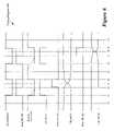
- FIG. 4illustrates a modified sense amplifier for one column of memory cells in a memory array, according to some embodiments of the invention.
- FIG. 5illustrates several sense amplifiers for several columns of memory cells in a memory array, according to some embodiments of the invention.
- FIG. 6illustrates a timing diagram according to some embodiments of the invention.
- the inventionis directed towards method and apparatus for accessing contents of memory cells.
- numerous detailsare set forth for purpose of explanation. However, one of ordinary skill in the art will realize that the invention may be practiced without the use of these specific details.
- the present inventionis primarily described below with reference to memory cells that store configuration data. However, the same techniques can easily be applied for other types of memory circuits and/or for storage of other types of data. In other instances, well-known structures and devices are shown in block diagram form in order not to obscure the description of the invention with unnecessary detail.
- Some embodiments of the inventionprovide a memory array for storing configuration data.
- the memory arrayincludes sets of buffer cells and sets of non-buffer cells.
- the sets of non-buffer cellsstore configuration data sets.
- the buffer cellsare used to provide continuous output of different configuration data sets that are stored in different non-buffer cells.
- some embodimentstransfer the contents of the particular set of non-buffer cells to a particular set of buffer cells.
- the particular buffer-cell setthen provides a continuous output of the particular configuration data set, through a set of output lines that connect to the particular buffer cell set.
- Some embodimentshave multiple sets of buffer cells to allow the transfer of at least one configuration data set to be interleaved with the continuous output of at least one other configuration data set. For instance, some embodiments have two buffer cell sets, so that one buffer cell set continuously outputs a first configuration data set of a first non buffer cell set, while another buffer cell set receives a second configuration data set from a second non buffer cell set.
- each buffer cell setconnects to a set of output lines that provide the continuous output of the content of the buffer cell set.
- the buffer cell setsare arranged along the periphery of the memory array. This arrangement simplifies the accessing of the buffer cells by the output lines that provide the continuous output of the configuration data sets that are stored in the buffer cells.
- FIG. 1illustrates a more detailed embodiment of a memory array 100 of the invention.
- the memory array 100includes N non-buffer rows 103 3 - 103 N , two buffer rows 101 and 102 , two sets of output lines 115 and 117 for the two buffer rows, a multiplexer 110 , and configuration output lines 113 .
- the buffer and non-buffer rowsare “logical” rows in the memory array.
- each logical rowis a separate physical row in the memory array.
- two or more logical rowsmight occupy an actual physical row in the memory array, while one logical row might occupy more than one physical row in the memory array.
- the buffer rowsare typically placed in one or more rows at or close to the periphery of the memory array.
- Each non-buffer rowstores a set of configuration data.
- the memory arrayshifts the particular configuration data set to a buffer row 101 or 102 .
- Attached to each buffer rowis a set of output lines 115 or 117 , which provides a continuous output of the contents of the buffer row. Accordingly, through the output lines that are attached to the buffer row that receives the shifted configuration data set, the memory can provide a continuous output of the configuration data set.
- the sets of output lines 115 and 117are supplied to the multiplexer 110 .
- the memoryuses the multiplexer 110 in order to interleave the outputting of the configuration data sets from one buffer row with the shifting of the configuration data sets to the other buffer row.
- FIG. 1illustrates that the configuration data set stored in non-buffer row 103 6 is initially shifted to buffer row 101 .
- the output lines 115 of the buffer row 101provide a continuous output of the configuration data set received from the non-buffer row 103 6 .
- the multiplexer 110can then be directed to connect the output of the buffer row 101 to the configuration output lines 113 .
- a configuration data setcan be shifted from the non-buffer row 103 8 to the buffer row 102 , while the buffer row 101 outputs its configuration data set.
- shiftingis accomplished through a modified sense amplifier that allows the reading and the writing of the contents of one cell in the memory array to another cell in the memory array to occur in a single cycle.
- a modified sense amplifierwill be described by reference to FIGS. 2-4 .
- FIG. 2illustrates one column 211 of cells in the memory array 100 of FIG. 1 .
- Column 211includes a bit line 214 , a complement bit line 216 , word lines 220 and 222 , memory cells 230 and 232 , and a sense amplifier 212 .
- Memory cells in an arrayare typically arranged in columns and rows that are typically accessible through bit lines and word lines.
- the cell 230is located between the bit lines 214 and 216 in the column 211 , along the row of cells connected to the word line 220 .
- the word line 220enables write and/or read operations for the cell 230 by using the sense amplifier 212 tied to the bit lines 214 and 216 .
- the column 211includes the sense amplifier 212 .
- This sense amplifier 212allows for the shifting of the contents of one cell to another cell in the column 211 in a single cycle. For instance, during the first part of a given clock cycle, the word line 220 may be activated. When the word line 220 is activated, the sense amplifier 212 may sense a data value stored in the cell 230 . Then, during a subsequent part of the same clock cycle, the word line 220 may be de-activated and the word line 222 may be activated instead.
- the sense amplifier 212may write that last sensed data value (from the cell 230 ) back along the bit lines 214 and 216 to another cell 232 in the column 211 , all in the same clock cycle.
- the cell 232may be a buffer cell that is wired with output lines 224 .
- FIG. 3illustrates a diagram of one column 311 of memory cells in a memory array that is known in the art. Each cell in the column 311 can be either written to, or read from, in a given cycle. However, to move the contents from one cell to another cell in the column 311 , the typical sense amplifier 312 requires multiple cycles (i.e., separate read and write cycles) and external hardware such as an external register for temporary data storage external to the memory array.
- the typical sense amplifier 312includes pass gates 342 and 344 , read isolation gates 346 and 348 , an enable_gate 358 , an amplifier stage 328 , a sense_amplifier_enable line (SA_EN) 313 , and input voltage (VDD) lines 317 , 318 , and 319 .
- SA_ENsense_amplifier_enable line
- VDDinput voltage
- the sense_amplifier_enable line 313is coupled to the gate-inputs of the pass gates 342 and 344 , the gate-inputs of the read isolation gates 346 and 348 , and the gate-input of the enable_gate 358 .
- the sense_amplifier_enable line 313enables the sense amplifier 312 by activating the pass gates 342 and 344 , and the read isolation gates 346 and 348 , to provide signal and power to the amplifier stage 328 , through the bit lines 314 and 316 .
- the amplifier stage 328is coupled to the VDD line 319 , to the enable_gate 358 , and to the bit lines 314 and 316 . As shown in FIG. 3 , the amplifier stage 328 is typically a pair of cross-coupled CMOS inverters 334 and 336 that are formed by two PMOS transistors 350 and 352 , and two NMOS transistors 354 and 356 . During a read operation, the amplifier stage 328 senses a value stored in the cell 330 through the bit lines 314 and 316 . The amplifier stage 328 then amplifies the sensed value by using power from the input VDD line 319 .
- the followingwill describe a read operation of the contents of the cell 330 by using the typical sense amplifier 312 .
- the voltage on the bit lines 314 and 316are pre-charged to a pre-determined level.
- the read isolation gates 346 and 348are turned on using the sense_amplifier_enable line 313 .
- a cell with an activated word linewill modify the pre-charged voltages on the bit lines 314 and 316 . In this manner, the cell will pass its contents in the form of voltages along the bit lines 314 and 316 , through the read isolation gates 346 and 348 , into the amplifier stage 328 .
- the word line 320is activated then the contents of the cell 330 will be “sensed” by the amplifier stage 328 of the sense amplifier 312 .
- the amplifier stage 328then pushes the values read from the cell 330 to the rails by using the power supplied by the VDD line 319 .
- the read isolation gates 346 and 348are typically then turned off (after sensing) to prevent the amplifier stage 328 from undesirably altering the contents of the memory cells in column 311 .
- the VDD line 319continues to provide power to the amplifier stage 328 .
- the sensed and amplified values in the amplifier stage 328will be pushed onto the bit lines 314 and 316 for reading at a location that is external to the column 311 and the memory array 300 .
- the external locationis typically a register or other temporary means to hold the contents of a first cell in the array until these contents can be written in a subsequent cycle to a second cell in the memory array. Accordingly, reading and writing back the contents of memory cells in this manner known in the art typically requires multiple clock cycles and external components such as a register.
- Some embodiments of the inventionsave clock cycle time and reduce hardware requirements over the art by shifting the contents of one cell to another cell in a single clock cycle without the need for an external temporary storage location. These embodiments will now be described in relation to FIG. 4 .
- FIG. 4illustrates a column 411 of cells.
- the column 411includes a non-buffer cell 430 , a buffer cell 432 , and a modified sense amplifier 412 , all coupled between a bit line 414 and a complement-bit line 416 .
- the non-buffer cell 430represents a cell in the non-buffer rows 103 3 - 103 8 illustrated in FIG. 1
- the buffer cell 432represents a buffer cell in the buffer rows 101 - 102 illustrated in FIG. 1 .
- the non-buffer cell 430is tied to the word line 420 while the buffer cell 432 is tied to the word line 422 , to enable read and write operations for these cells.
- FIG. 4also illustrates the modified sense amplifier 412 , according to some embodiments of the invention.
- the modified sense amplifier 412is similar to the typical sense amplifier 312 illustrated in FIG. 3 , in that it provides read and write operations for buffer and non-buffer cells in the column 411 .
- the modified sense amplifier 412differs from the typical sense amplifier 312 in that it does not include the read isolation gates 346 and 348 .
- the read isolation gates 346 and 348isolate the typical sense amplifier 312 after the sensing stage of a read operation to prevent unintended write back to the cells in the column 311 illustrated in FIG. 3 .
- the modified sense amplifier 412 shown in FIG. 4allows the bit lines to be driven high (back up to the rails) after the sensing stage of a read operation.
- the modified sense amplifier 412 of the illustrated embodimentthen uses the bit lines to write the contents of a first cell (the cell that was read) to a second cell, in the same cycle as the read operation for the first cell.
- the modified sense amplifier 412further includes a precharge-bar line 460 coupled to precharge transistors 462 and 464 .
- the precharge transistors 462 and 464can be PMOS transistors and can be used to supply faster charging to the bit lines 414 and 416 . Rapid charging of the bit lines may be desired, for example, in order to execute both a read and write operation in the same clock cycle.
- An example where the modified sense amplifier 412 both reads from the cell 430 and writes to the cell 432 (a “shifting” operation)will now be described.
- both bit linesare driven to a predetermined level and then subsequently allowed to graduate toward a value stored in a cell with an activated word line. For instance, after initial pre-charging, the bit line 414 can be pulled high and the complement bit line 416 can be pulled low by the value stored in the cell 430 .
- the precharge-bar line 460may be used to drive the initial values on these bit lines 414 and 416 .
- the word line 420can be activated to allow the value of the cell 430 to be sensed and amplified by the amplifier stage 428 through the bit lines 414 and 416 . Once the value in the cell 430 is sensed by the amplifier stage 428 , the word line 420 and the precharge-bar line 460 can be de-activated.
- the modified sense amplifier 412has no read isolation gates, the value sensed from the cell 430 at the amplifier stage 428 can be driven back along the bit lines 414 and 416 to the memory cells in the column 411 .
- This feedback signal along the bit lines 414 and 416is similar to the write signal during a typical write operation, where both bit lines are driven high, then one bit line is brought low to write the value on the bit lines into the cell with the activated word line.
- the word line 422can be activated to write into the cell 432 the value previously sensed by the amplifier stage 428 (through the bit lines 414 and 416 ).
- the buffer cell 432is wired with the configuration output 424 , the shifted contents of the non-buffer cell 430 are immediately available at the configuration output 424 of the buffer cell 432 .
- the process described abovecan be repeated across all the cells coupled to a given word line to shift an entire first row of cells in a memory array to a second row of cells in the array.
- the first rowcan be a non-buffer row such as rows 103 3 - 103 8 in FIG. 1 .
- the second rowcan be a buffer row such as rows 101 - 102 in FIG. 1 .
- FIG. 5illustrates several sense amplifiers for several columns of cells in a memory array 500 , according to some embodiments of the invention.
- the memory array 500includes a precharge line 560 , a sense_amplifier enable line (SA_EN) 513 , read_word lines (Read_WL) 520 and 521 write_word lines (Write_WL) 522 and 525 , and a cell column 511 .
- the column 511includes non-buffer cells 530 and 531 , and buffer cells 532 and 535 . This column 511 illustrates a more detailed embodiment of the column 211 in FIG. 2 , and the array 500 illustrates a more detailed embodiment of the array 100 in FIG. 1 .
- each cell in a first row in the array 500can be shifted to the cells in a second row in the array 500 by using the method described in relation to FIG. 4 .
- the read_word line 520connects a non-buffer cell in each column of the memory array 500 , to form a non-buffer row of memory cells in the array 500
- the write_word line 522connects a buffer cell in each column of the memory array 500 , to form a buffer row of cells in the array 500 .
- the read_word line 520 and the write_word line 522can each be activated in sequence within the same cycle such that the contents of the non-buffer row coupled to the read_word line 520 can be read in a first part of a cycle and written to the buffer row coupled to the write_word line 522 , in a second part of the same cycle.
- the memory array 500performs this shifting of the contents of the cells in each row by using the modified sense amplifier 512 of some embodiments, as previously described in relation to FIG. 4 .
- the buffer row cells of some embodimentsare wired with configuration output lines to allow their contents to be outputted from the memory array 500 , without the need for a read operation. Shifting to and outputting by the separate buffer rows containing the buffer cells 532 and 535 , respectively, can be interleaved such that the contents of any given row is outputted by one of the buffer rows in any given cycle.
- the operation of the memory array 500will be further described in relation to the timing diagram illustrated in FIG. 6 .
- FIG. 6illustrates a timing diagram 600 according to some embodiments of the invention.
- the timing diagram 600includes a pre-charge signal 660 , a read_word_line signal (Read_WL) 620 , bit signals 614 and 616 , a sense_amplifier_enable signal (SA_EN) 613 , write_word_line signals (Write_WL) 622 and 625 , and configuration_output signals (Cfg_out) 624 and 626 .
- the pre-charge signal 660represents the signal through the pre-charge line 560 in FIG. 5 .
- the pre-charge signal 660allows the bit signals 614 and 616 to be quickly charged, for instance, prior to a read or a write operation.
- the read_word_line signal 620represents the signal through the word line 520 in FIG. 5 .
- the read_word_line signal 620allows read access to the cells in a row coupled to the word line 520 .
- the bit signals 614 and 616represent the signals through the bit lines 514 and 516 in FIG. 5 .
- the bit signals 614 and 616provide a differential signal for the cells in a column of a memory array and for a sense amplifier coupled to the cells in the column of the memory array.
- the sense_amplifier_enable signal (SA_EN) 613represents the signal through the sense_amplifier_enable line 513 in FIG. 5 .
- the sense_amplifier_enable signal 613enables the sense amplifier 512 for a read or write operation to, or from, the cells that are coupled to the sense amplifier 512 by the bit lines 514 and 516 .
- the write_word_line signal (Write_WL) 622represents a signal through the word line 522 in FIG. 5 .
- the write_word_line signal 622enables a write operation for the row of cells that are coupled to the word line 522 .
- the configuration_output signal (Cfg_out) 624represents a signal through the configuration_output lines 524 in FIG. 5 .
- the configuration_output signal 624can provide the value stored in the buffer cell 532 (i.e., the “configuration” of the buffer cell 532 ) to a location outside of the memory array 500 .
- the write_word_line signal (Write_WL) 625represents a signal through the word line 525 in FIG. 5 .
- the write_word_line signal 625enables a write operation for the row of cells that are coupled to the word line 525 .
- the configuration_output signal (Cfg_out) 626represents a signal through the configuration_output lines 526 in FIG. 5 .
- the configuration_output signal 626can provide the value stored in the buffer cell 535 (the “configuration” of the buffer cell 535 ) to a location outside of the memory array 500 .
- FIG. 6further illustrates two clock cycles.
- the first clock cycleindicated by the times t 0 to t 5
- the contents of the non-buffer cell 530are shifted to the buffer cell 532 in FIG. 5 .
- the second clock cycleindicated by the times t 5 to t 10
- the contents of the non-buffer cell 530are shifted to the buffer cell 535 .
- the pre-charge signal 660 and the bit signals 614 and 616are driven high (have a logical “1”) in preparation of a read/write operation.
- the read_word_line signal 620 , the sense_amplifier_enable signal 613 , and the write_word_line signals 622 and 625are low (have a logical “0”).
- the configuration_output signals 624 and 626each have one high and one low output at their pairs of output lines 524 and 526 .
- the precharge signal 660is brought low and one of the bit signals 614 and 616 is subsequently pulled lower by the stored voltage that, in some embodiments, represents the contents of the cell 530 . In other embodiments, one of the bit signals 614 and 616 is pulled lower by the stored voltage that represents the complement value stored by the cell 530 . Also at t 1 , the read_word_line signal 620 and the sense_amplifier_enable signal 613 are driven high (are “enabled”). The foregoing allows the value in the cell 530 to be read or “sensed” by the sense amplifier 512 through the bit lines 514 and 516 in FIG. 5 .
- the read_word_line signal 620is brought low and the write_word_line signal 622 is driven high. This allows the value “sensed” by the sense amplifier 512 at t 1 to be written (or “shifted”) to the cell 532 shown in FIG. 5 . As shown by dashed lines in FIG. 6 , previously in the art, the read_word_line signal 620 was driven high for much of the clock cycle from t 0 to t 5 . However, in the described embodiment, the read_word_line signal 620 is driven high for less than the duration of a clock cycle in order to share the clock cycle from t 0 to t 5 with the write_word_line signal 622 .
- the pair of configuration_output signals 624reverse their values to represent that the contents of the buffer cell 532 have been over-written by the sense amplifier 512 and that the configuration_output lines 524 are now outputting the new value and its complement from the buffer cell 532 .
- the precharge signal 660 and the bit signals 614 and 616are driven high again in preparation of another read/write operation.
- the sense_amplifier_enable signal 613 and the write_word_line signal 622are brought low to disable sensing by the sense amplifier 512 and to disable writing to the cell 532 , respectively.
- the first clock cycleends and the second clock cycle begins.
- the sequencerepeats to shift the contents of the non-buffer cell 530 into the buffer cell 535 .
- the contents of the non-buffer cell 530are sensed by the sense amplifier 512 .
- the sensed valuesare written to the buffer cell 535 .
- the configuration_output signal 626reflects the changed contents of the buffer cell 535 .
- the precharging of the bit lines 514 and 516represented by the precharge signal 660 , resumes in preparation of the next read/write operation.
- the second cycleconcludes at t 10 , where a third cycle may commence.
- Sensing (and thus shifting) from the same source cell 530is illustrated for both the first and second clock cycles to simplify the timing diagram 500 .
- FIG. 5is representative. Thus, shifting from a source cell other than the cell 530 can occur in either the first or second clock cycle shown in FIG. 5 .
- the present inventionprovides several advantages over the prior art. For instance, the present invention allows shifting of data between cells in a memory array in a single clock cycle. Shifting can occur for all of the cells in a non-buffer row to a buffer row of cells. Given multiple buffer rows, shifting to the multiple buffer rows can be time multiplexed (interleaved) such that the contents of a different non-buffer row can be shifted to a buffer row in every cycle. Thus, the contents of a different row of cells is available at one of the buffer rows at every cycle.
- a normal modify memory operationrequires reading out to a register, modifying the contents of the register, and then writing back to the memory location.
- the contents of a cell and row of cellscould be modified in a single cycle completely within memory. For instance, a bit-mask could be applied to the contents of the source row before the contents are written back to a destination row. Further, if the destination row is a buffer row, then those modified contents would be available immediately at the configuration outputs of that buffer row.
- Several rows of the memory arraycan be designated as buffer rows and wired out for outputting the data contained in these rows. In some embodiments these rows are near the periphery of the memory array. Reading (outputting) from one peripheral row to the output lines and shifting to another peripheral row can occur in the same clock cycle. Since outputting and shifting is effectively time multiplexed across multiple buffer rows, the contents of an entire memory array can be outputted rapidly in succession. Moreover, the memory array is no longer limited in depth because the present invention eliminates the need to wire the internal nodes of the array with additional output lines.
Landscapes
- Dram (AREA)
- Static Random-Access Memory (AREA)
Abstract
Description
Claims (10)
Priority Applications (1)
| Application Number | Priority Date | Filing Date | Title |
|---|---|---|---|
| US11/745,442US7804730B2 (en) | 2005-03-15 | 2007-05-07 | Method and apparatus for accessing contents of memory cells |
Applications Claiming Priority (2)
| Application Number | Priority Date | Filing Date | Title |
|---|---|---|---|
| US11/081,870US7230869B1 (en) | 2005-03-15 | 2005-03-15 | Method and apparatus for accessing contents of memory cells |
| US11/745,442US7804730B2 (en) | 2005-03-15 | 2007-05-07 | Method and apparatus for accessing contents of memory cells |
Related Parent Applications (1)
| Application Number | Title | Priority Date | Filing Date |
|---|---|---|---|
| US11/081,870ContinuationUS7230869B1 (en) | 2005-03-15 | 2005-03-15 | Method and apparatus for accessing contents of memory cells |
Publications (2)
| Publication Number | Publication Date |
|---|---|
| US20070242529A1 US20070242529A1 (en) | 2007-10-18 |
| US7804730B2true US7804730B2 (en) | 2010-09-28 |
Family
ID=38120553
Family Applications (2)
| Application Number | Title | Priority Date | Filing Date |
|---|---|---|---|
| US11/081,870Expired - Fee RelatedUS7230869B1 (en) | 2005-03-15 | 2005-03-15 | Method and apparatus for accessing contents of memory cells |
| US11/745,442Expired - LifetimeUS7804730B2 (en) | 2005-03-15 | 2007-05-07 | Method and apparatus for accessing contents of memory cells |
Family Applications Before (1)
| Application Number | Title | Priority Date | Filing Date |
|---|---|---|---|
| US11/081,870Expired - Fee RelatedUS7230869B1 (en) | 2005-03-15 | 2005-03-15 | Method and apparatus for accessing contents of memory cells |
Country Status (1)
| Country | Link |
|---|---|
| US (2) | US7230869B1 (en) |
Cited By (13)
| Publication number | Priority date | Publication date | Assignee | Title |
|---|---|---|---|---|
| US7948266B2 (en) | 2004-02-14 | 2011-05-24 | Tabula, Inc. | Non-sequentially configurable IC |
| US8112468B1 (en) | 2007-03-22 | 2012-02-07 | Tabula, Inc. | Method and apparatus for performing an operation with a plurality of sub-operations in a configurable IC |
| US8117436B2 (en) | 2006-04-19 | 2012-02-14 | Queen's University At Kingston | Hybrid nanotube/CMOS dynamically reconfigurable architecture and an integrated design optimization method and system therefor |
| US8138789B2 (en) | 2007-09-06 | 2012-03-20 | Tabula, Inc. | Configuration context switcher with a clocked storage element |
| US8159264B2 (en) | 2004-11-08 | 2012-04-17 | Tabula, Inc. | Storage elements for a configurable IC and method and apparatus for accessing data stored in the storage elements |
| US8193830B2 (en) | 2004-02-14 | 2012-06-05 | Tabula, Inc. | Configurable circuits, IC's, and systems |
| US8842475B2 (en) | 2012-03-28 | 2014-09-23 | Kabushiki Kaisha Toshiba | Configuration memory |
| US20150228324A1 (en)* | 2014-02-07 | 2015-08-13 | Semiconductor Energy Laboratory Co., Ltd. | Semiconductor device |
| US9530502B2 (en) | 2014-03-20 | 2016-12-27 | Kabushiki Kaisha Toshiba | Configuration memory storing data by injecting carriers in gate insulating layer of MISFET |
| US9543957B2 (en) | 2013-07-24 | 2017-01-10 | Kabushiki Kaisha Toshiba | Reconfigurable logic circuit device |
| US9621159B2 (en) | 2014-09-19 | 2017-04-11 | Kabushiki Kaisha Toshiba | Reconfigurable semiconductor integrated circuit and electronic device |
| US9691476B2 (en) | 2013-07-26 | 2017-06-27 | Kabushiki Kaisha Toshiba | Multi-context configuration memory |
| US10937481B1 (en)* | 2019-08-07 | 2021-03-02 | Arm Limited | Polarity swapping circuitry |
Families Citing this family (16)
| Publication number | Priority date | Publication date | Assignee | Title |
|---|---|---|---|---|
| US7268586B1 (en) | 2004-11-08 | 2007-09-11 | Tabula, Inc. | Method and apparatus for accessing stored data in a reconfigurable IC |
| US7230869B1 (en)* | 2005-03-15 | 2007-06-12 | Jason Redgrave | Method and apparatus for accessing contents of memory cells |
| US7272031B1 (en)* | 2005-03-15 | 2007-09-18 | Tabula, Inc. | Method and apparatus for reduced power cell |
| US7443196B2 (en)* | 2005-07-15 | 2008-10-28 | Tabula, Inc. | Configuration network for a configurable IC |
| US7529992B1 (en) | 2006-03-27 | 2009-05-05 | Tabula, Inc. | Configurable integrated circuit with error correcting circuitry |
| US7669097B1 (en) | 2006-03-27 | 2010-02-23 | Tabula, Inc. | Configurable IC with error detection and correction circuitry |
| US8412990B2 (en)* | 2007-06-27 | 2013-04-02 | Tabula, Inc. | Dynamically tracking data values in a configurable IC |
| US7839162B2 (en) | 2007-06-27 | 2010-11-23 | Tabula, Inc. | Configurable IC with deskewing circuits |
| US8069425B2 (en) | 2007-06-27 | 2011-11-29 | Tabula, Inc. | Translating a user design in a configurable IC for debugging the user design |
| US8990651B2 (en)* | 2007-09-19 | 2015-03-24 | Tabula, Inc. | Integrated circuit (IC) with primary and secondary networks and device containing such an IC |
| WO2010016857A1 (en) | 2008-08-04 | 2010-02-11 | Tabula, Inc. | Trigger circuits and event counters for an ic |
| US8072234B2 (en) | 2009-09-21 | 2011-12-06 | Tabula, Inc. | Micro-granular delay testing of configurable ICs |
| KR101970712B1 (en) | 2012-08-23 | 2019-04-22 | 삼성전자주식회사 | Device and method for moving data in terminal |
| US9154137B2 (en) | 2013-07-04 | 2015-10-06 | Altera Corporation | Non-intrusive monitoring and control of integrated circuits |
| US10153042B2 (en) | 2013-11-28 | 2018-12-11 | Gsi Technology Inc. | In-memory computational device with bit line processors |
| US9418719B2 (en)* | 2013-11-28 | 2016-08-16 | Gsi Technology Israel Ltd. | In-memory computational device |
Citations (196)
| Publication number | Priority date | Publication date | Assignee | Title |
|---|---|---|---|---|
| US4873459A (en) | 1986-09-19 | 1989-10-10 | Actel Corporation | Programmable interconnect architecture |
| US5150326A (en)* | 1989-10-23 | 1992-09-22 | Nec Corporation | Register file capable of high speed read operation |
| US5245575A (en)* | 1990-09-07 | 1993-09-14 | Nec Corporation | Register circuit for copying contents of one register into another register |
| US5270581A (en) | 1991-04-15 | 1993-12-14 | Nec Corporation | Semiconductor integrated circuit device having step-down circuit associated with component circuits arranged in low-power consumption manner |
| US5325329A (en)* | 1991-12-03 | 1994-06-28 | Mitsubishi Denki Kabushiki Kaisha | Dual port memory effecting transfer of data between a serial register and an arbitrary memory block |
| US5329498A (en) | 1993-05-17 | 1994-07-12 | Hewlett-Packard Company | Signal conditioning and interconnection for an acoustic transducer |
| US5349250A (en) | 1993-09-02 | 1994-09-20 | Xilinx, Inc. | Logic structure and circuit for fast carry |
| US5357153A (en) | 1993-01-28 | 1994-10-18 | Xilinx, Inc. | Macrocell with product-term cascade and improved flip flop utilization |
| US5365125A (en) | 1992-07-23 | 1994-11-15 | Xilinx, Inc. | Logic cell for field programmable gate array having optional internal feedback and optional cascade |
| US5369622A (en) | 1993-04-20 | 1994-11-29 | Micron Semiconductor, Inc. | Memory with isolated digit lines |
| US5371708A (en)* | 1992-03-26 | 1994-12-06 | Nec Corporation | FIFO-type semiconductor device |
| US5426378A (en) | 1994-04-20 | 1995-06-20 | Xilinx, Inc. | Programmable logic device which stores more than one configuration and means for switching configurations |
| US5521835A (en) | 1992-03-27 | 1996-05-28 | Xilinx, Inc. | Method for programming an FPLD using a library-based technology mapping algorithm |
| US5532958A (en)* | 1990-06-25 | 1996-07-02 | Dallas Semiconductor Corp. | Dual storage cell memory |
| US5544078A (en)* | 1988-06-17 | 1996-08-06 | Dallas Semiconductor Corporation | Timekeeping comparison circuitry and dual storage memory cells to detect alarms |
| US5552721A (en) | 1995-06-05 | 1996-09-03 | International Business Machines Corporation | Method and system for enhanced drive in programmmable gate arrays |
| US5581500A (en) | 1994-12-16 | 1996-12-03 | Sun Microsystems, Inc. | Memory cell with power supply induced reversed-bias pass transistors for reducing off-leakage current |
| US5600263A (en) | 1995-08-18 | 1997-02-04 | Xilinx, Inc. | Configuration modes for a time multiplexed programmable logic device |
| US5629637A (en) | 1995-08-18 | 1997-05-13 | Xilinx, Inc. | Method of time multiplexing a programmable logic device |
| US5631578A (en) | 1995-06-02 | 1997-05-20 | International Business Machines Corporation | Programmable array interconnect network |
| US5640106A (en) | 1995-05-26 | 1997-06-17 | Xilinx, Inc. | Method and structure for loading data into several IC devices |
| US5646545A (en) | 1995-08-18 | 1997-07-08 | Xilinx, Inc. | Time multiplexed programmable logic device |
| US5646544A (en) | 1995-06-05 | 1997-07-08 | International Business Machines Corporation | System and method for dynamically reconfiguring a programmable gate array |
| US5659484A (en) | 1993-03-29 | 1997-08-19 | Xilinx, Inc. | Frequency driven layout and method for field programmable gate arrays |
| US5682107A (en) | 1994-04-01 | 1997-10-28 | Xilinx, Inc. | FPGA architecture with repeatable tiles including routing matrices and logic matrices |
| US5692147A (en) | 1995-06-07 | 1997-11-25 | International Business Machines Corporation | Memory mapping method and apparatus to fold sparsely populated structures into densely populated memory columns or rows by selectively transposing X and Y address portions, and programmable gate array applications thereof |
| US5701441A (en) | 1995-08-18 | 1997-12-23 | Xilinx, Inc. | Computer-implemented method of optimizing a design in a time multiplexed programmable logic device |
| US5719889A (en) | 1995-12-20 | 1998-02-17 | International Business Machines Corporation | Programmable parity checking and comparison circuit |
| US5721498A (en) | 1995-12-11 | 1998-02-24 | Hewlett Packard Company | Block segmentation of configuration lines for fault tolerant programmable logic device |
| US5732246A (en) | 1995-06-07 | 1998-03-24 | International Business Machines Corporation | Programmable array interconnect latch |
| US5734622A (en) | 1992-09-11 | 1998-03-31 | Fujitsu Limited | MOS static RAM with improved soft error resistance; high-level supply voltage drop detection circuit and complementary signal transition detection circuit for the same; and semiconductor device with improved intersignal time margin |
| US5737235A (en) | 1995-05-02 | 1998-04-07 | Xilinx Inc | FPGA with parallel and serial user interfaces |
| US5745422A (en) | 1996-11-12 | 1998-04-28 | International Business Machines Corporation | Cross-coupled bitline segments for generalized data propagation |
| US5745734A (en) | 1995-09-29 | 1998-04-28 | International Business Machines Corporation | Method and system for programming a gate array using a compressed configuration bit stream |
| US5761483A (en) | 1995-08-18 | 1998-06-02 | Xilinx, Inc. | Optimizing and operating a time multiplexed programmable logic device |
| US5760602A (en) | 1996-01-17 | 1998-06-02 | Hewlett-Packard Company | Time multiplexing a plurality of configuration settings of a programmable switch element in a FPGA |
| US5764954A (en) | 1995-08-23 | 1998-06-09 | International Business Machines Corporation | Method and system for optimizing a critical path in a field programmable gate array configuration |
| US5768178A (en)* | 1995-06-30 | 1998-06-16 | Micron Technology, Inc. | Data transfer circuit in a memory device |
| US5777360A (en) | 1994-11-02 | 1998-07-07 | Lsi Logic Corporation | Hexagonal field programmable gate array architecture |
| US5802003A (en) | 1995-12-20 | 1998-09-01 | International Business Machines Corporation | System for implementing write, initialization, and reset in a memory array using a single cell write port |
| US5815726A (en) | 1994-11-04 | 1998-09-29 | Altera Corporation | Coarse-grained look-up table architecture |
| US5847577A (en) | 1995-02-24 | 1998-12-08 | Xilinx, Inc. | DRAM memory cell for programmable logic devices |
| US5889411A (en) | 1997-02-26 | 1999-03-30 | Xilinx, Inc. | FPGA having logic element carry chains capable of generating wide XOR functions |
| US5914616A (en) | 1997-02-26 | 1999-06-22 | Xilinx, Inc. | FPGA repeatable interconnect structure with hierarchical interconnect lines |
| US5914906A (en) | 1995-12-20 | 1999-06-22 | International Business Machines Corporation | Field programmable memory array |
| US5940603A (en) | 1993-06-24 | 1999-08-17 | Quickturn Design Systems, Inc. | Method and apparatus for emulating multi-ported memory circuits |
| US5944813A (en) | 1993-08-03 | 1999-08-31 | Xilinx, Inc. | FPGA input output buffer with registered tristate enable |
| US5970240A (en) | 1997-06-25 | 1999-10-19 | Quickturn Design Systems, Inc. | Method and apparatus for configurable memory emulation |
| US5982655A (en) | 1998-09-29 | 1999-11-09 | Cisco Technology, Inc. | Method and apparatus for support of multiple memory types in a single memory socket architecture |
| US5991191A (en) | 1997-12-05 | 1999-11-23 | Silicon Aquarius, Inc. | Methods and circuits for single-memory cell multivalue data storage |
| US6002991A (en) | 1996-08-30 | 1999-12-14 | Xilinx, Inc. | Method and apparatus for measuring localized voltages on programmable integrated circuits |
| US6054873A (en) | 1996-12-05 | 2000-04-25 | International Business Machines Corporation | Interconnect structure between heterogeneous core regions in a programmable array |
| US6057707A (en) | 1997-06-20 | 2000-05-02 | Altera Corporation | Programmable logic device incorporating a memory efficient interconnection device |
| US6069490A (en) | 1997-12-02 | 2000-05-30 | Xilinx, Inc. | Routing architecture using a direct connect routing mesh |
| US6084429A (en) | 1998-04-24 | 2000-07-04 | Xilinx, Inc. | PLD having a window pane architecture with segmented and staggered interconnect wiring between logic block arrays |
| US6086631A (en) | 1998-04-08 | 2000-07-11 | Xilinx, Inc. | Post-placement residual overlap removal method for core-based PLD programming process |
| US6091263A (en) | 1997-12-12 | 2000-07-18 | Xilinx, Inc. | Rapidly reconfigurable FPGA having a multiple region architecture with reconfiguration caches useable as data RAM |
| US6107821A (en) | 1999-02-08 | 2000-08-22 | Xilinx, Inc. | On-chip logic analysis and method for using the same |
| US6110223A (en) | 1996-10-28 | 2000-08-29 | Altera Corporation | Graphic editor for block diagram level design of circuits |
| US6111779A (en) | 1998-05-07 | 2000-08-29 | Lg Semicon Co., Ltd. | Cell structure for low electric power static RAM |
| US6134154A (en) | 1998-04-03 | 2000-10-17 | Nec Corporation | Semiconductor memory device with several access enabled using single port memory cell |
| US6140839A (en) | 1998-05-13 | 2000-10-31 | Kaviani; Alireza S. | Computational field programmable architecture |
| US6150838A (en) | 1999-02-25 | 2000-11-21 | Xilinx, Inc. | FPGA configurable logic block with multi-purpose logic/memory circuit |
| US6163168A (en) | 1998-12-09 | 2000-12-19 | Vantis Corporation | Efficient interconnect network for use in FPGA device having variable grain architecture |
| US6166946A (en)* | 2000-01-21 | 2000-12-26 | Hewlett-Packard Company | System and method for writing to and reading from a memory cell |
| US6173379B1 (en)* | 1996-05-14 | 2001-01-09 | Intel Corporation | Memory device for a microprocessor register file having a power management scheme and method for copying information between memory sub-cells in a single clock cycle |
| US6172521B1 (en) | 1997-04-11 | 2001-01-09 | Nec Corporation | Programmable logic IC having memories for previously storing a plurality of configuration data and a method of reconfigurating same |
| US6175247B1 (en) | 1998-04-14 | 2001-01-16 | Lockheed Martin Corporation | Context switchable field programmable gate array with public-private addressable sharing of intermediate data |
| US6184709B1 (en) | 1996-04-09 | 2001-02-06 | Xilinx, Inc. | Programmable logic device having a composable memory array overlaying a CLB array |
| US6184707B1 (en) | 1998-10-07 | 2001-02-06 | Altera Corporation | Look-up table based logic element with complete permutability of the inputs to the secondary signals |
| US6204687B1 (en) | 1999-08-13 | 2001-03-20 | Xilinx, Inc. | Method and structure for configuring FPGAS |
| US6205076B1 (en) | 1998-03-27 | 2001-03-20 | Fujitsu Limited | Destructive read type memory circuit, restoring circuit for the same and sense amplifier |
| US6229337B1 (en) | 1999-06-15 | 2001-05-08 | Ict Acquisition, Inc. | High-density programmable logic device with flexible local connections and multiplexer based global interconnections |
| US6255849B1 (en) | 2000-02-04 | 2001-07-03 | Xilinx, Inc. | On-chip self-modification for PLDs |
| US20010007428A1 (en) | 1997-02-26 | 2001-07-12 | Young Steven P. | Interconnect structure for a programmable logic device |
| US6275064B1 (en) | 1997-12-22 | 2001-08-14 | Vantis Corporation | Symmetrical, extended and fast direct connections between variable grain blocks in FPGA integrated circuits |
| US20010013797A1 (en) | 2000-01-31 | 2001-08-16 | Sony Corporation | Logic cell and logic circuit using the same |
| US6292019B1 (en) | 1999-05-07 | 2001-09-18 | Xilinx Inc. | Programmable logic device having configurable logic blocks with user-accessible input multiplexers |
| US20010038552A1 (en) | 2000-03-24 | 2001-11-08 | Kabushiki Kaisha Toshiba | Semiconductor memory with switches for reducing leakage current |
| US6326651B1 (en) | 1999-03-08 | 2001-12-04 | Matsushita Electric Industrial Co., Ltd. | Field-programmable gate array with ferroelectric thin film |
| US6326807B1 (en) | 1997-03-21 | 2001-12-04 | Altera Corporation | Programmable logic architecture incorporating a content addressable embedded array block |
| US20020010853A1 (en) | 1995-08-18 | 2002-01-24 | Xilinx, Inc. | Method of time multiplexing a programmable logic device |
| US6346824B1 (en) | 1996-04-09 | 2002-02-12 | Xilinx, Inc. | Dedicated function fabric for use in field programmable gate arrays |
| US6348813B1 (en) | 1999-06-06 | 2002-02-19 | Lattice Semiconductor Corporation | Scalable architecture for high density CPLD's having two-level hierarchy of routing resources |
| US20020049955A1 (en) | 2000-09-06 | 2002-04-25 | Hitachi, Ltd. | Logic circuit design method and cell library for use therewith |
| US6381732B1 (en) | 1999-01-14 | 2002-04-30 | Xilinx, Inc. | FPGA customizable to accept selected macros |
| US6404224B1 (en) | 1995-12-19 | 2002-06-11 | Fujitsu Limited | Chain-connected shift register and programmable logic circuit whose logic function is changeable in real time |
| US6411128B2 (en) | 1999-12-10 | 2002-06-25 | Nec Corporation | Logical circuit for serializing and outputting a plurality of signal bits simultaneously read from a memory cell array or the like |
| US6414880B1 (en)* | 2000-08-23 | 2002-07-02 | Nec Corporation | Multiple line buffer type memory LSI |
| US6430736B1 (en) | 1999-02-26 | 2002-08-06 | Xilinx, Inc. | Method and apparatus for evolving configuration bitstreams |
| US20020113619A1 (en) | 2000-08-04 | 2002-08-22 | Leopard Logic, Inc. | Interconnection network for a Field Progammable Gate Array |
| US20020125910A1 (en) | 1999-02-25 | 2002-09-12 | Xilinx, Inc. | Configurable logic element with expander structures |
| US20020125914A1 (en) | 2001-03-08 | 2002-09-12 | Lg Electronics Inc. | Glitch free clock multiplexer circuit and method thereof |
| US6469540B2 (en) | 2000-06-15 | 2002-10-22 | Nec Corporation | Reconfigurable device having programmable interconnect network suitable for implementing data paths |
| US6469553B1 (en) | 1999-01-08 | 2002-10-22 | Altera Corporation | Phase-locked loop circuitry for programmable logic devices |
| US20020157071A1 (en) | 2001-04-13 | 2002-10-24 | Schiefele Walter P. | Method for creating circuit redundancy in programmable logic devices |
| US20020161568A1 (en) | 1997-05-30 | 2002-10-31 | Quickturn Design Systems, Inc. | Memory circuit for use in hardware emulation system |
| US20020163357A1 (en) | 1993-08-03 | 2002-11-07 | Btr, Inc. | Architecture and interconnect scheme for programmable logic circuits |
| US6487709B1 (en) | 2000-02-09 | 2002-11-26 | Xilinx, Inc. | Run-time routing for programmable logic devices |
| US6490707B1 (en) | 2000-07-13 | 2002-12-03 | Xilinx, Inc. | Method for converting programmable logic devices into standard cell devices |
| US6496918B1 (en) | 1996-04-11 | 2002-12-17 | Massachusetts Institute Of Technology | Intermediate-grain reconfigurable processing device |
| US6501698B1 (en)* | 2000-11-01 | 2002-12-31 | Enhanced Memory Systems, Inc. | Structure and method for hiding DRAM cycle time behind a burst access |
| US6515509B1 (en) | 2000-07-13 | 2003-02-04 | Xilinx, Inc. | Programmable logic device structures in standard cell devices |
| US6515505B1 (en) | 1995-12-26 | 2003-02-04 | Cypress Semiconductor Corp. | Functionality change by bond optioning decoding |
| US6529040B1 (en) | 2000-05-05 | 2003-03-04 | Xilinx, Inc. | FPGA lookup table with speed read decoder |
| US20030042931A1 (en) | 1993-08-03 | 2003-03-06 | Ting Benjamin S. | Architecture and interconnect scheme for programmable logic circuits |
| US6545501B1 (en) | 2001-12-10 | 2003-04-08 | International Business Machines Corporation | Method and system for use of a field programmable function within a standard cell chip for repair of logic circuits |
| US6560139B2 (en) | 2001-03-05 | 2003-05-06 | Intel Corporation | Low leakage current SRAM array |
| US20030110430A1 (en) | 2001-12-10 | 2003-06-12 | International Business Machines Corporation | Method and system for use of a field programmable gate array (FPGA) function within an application specific integrated circuit (ASIC) to enable creation of a debugger client within the ASIC |
| US20030122578A1 (en) | 2001-12-28 | 2003-07-03 | Shoichi Masui | Programmable logic device with ferroelectric configuration memories |
| US6593771B2 (en) | 2001-12-10 | 2003-07-15 | International Business Machines Corporation | Method and system for use of a field programmable interconnect within an ASIC for configuring the ASIC |
| US6601227B1 (en) | 2001-06-27 | 2003-07-29 | Xilinx, Inc. | Method for making large-scale ASIC using pre-engineered long distance routing structure |
| US6603330B1 (en) | 2000-10-26 | 2003-08-05 | Cypress Semiconductor Corporation | Configuring digital functions in a digital configurable macro architecture |
| US6629308B1 (en) | 2000-07-13 | 2003-09-30 | Xilinx, Inc. | Method for managing database models for reduced programmable logic device components |
| US6636070B1 (en) | 1997-10-16 | 2003-10-21 | Altera Corp | Driver circuitry for programmable logic devices with hierarchical interconnection resources |
| US6642744B2 (en) | 2000-03-10 | 2003-11-04 | Easic Corporation | Customizable and programmable cell array |
| US6643173B2 (en) | 2001-11-09 | 2003-11-04 | Oki Electric Industry Co., Ltd. | Semiconductor memory device operating in low power supply voltage and low power consumption |
| US6650142B1 (en) | 2002-08-13 | 2003-11-18 | Lattice Semiconductor Corporation | Enhanced CPLD macrocell module having selectable bypass of steering-based resource allocation and methods of use |
| US6668361B2 (en) | 2001-12-10 | 2003-12-23 | International Business Machines Corporation | Method and system for use of a field programmable function within a chip to enable configurable I/O signal timing characteristics |
| US6667635B1 (en) | 2002-09-10 | 2003-12-23 | Xilinx, Inc. | FPGA lookup table with transmission gate structure for reliable low-voltage operation |
| US6675309B1 (en) | 2000-07-13 | 2004-01-06 | Xilinx, Inc. | Method for controlling timing in reduced programmable logic devices |
| US20040010767A1 (en) | 2002-07-12 | 2004-01-15 | Lattice Semiconductor Corporation | Hierarchical general interconnect architecture for high density fpga's |
| US6686769B1 (en) | 2001-12-14 | 2004-02-03 | Altera Corporation | Programmable I/O element circuit for high speed logic devices |
| US6714041B1 (en) | 2002-08-30 | 2004-03-30 | Xilinx, Inc. | Programming on-the-fly (OTF) |
| US6717436B2 (en) | 1999-09-29 | 2004-04-06 | Infineon Technologies Ag | Reconfigurable gate array |
| US6724648B2 (en) | 2002-04-05 | 2004-04-20 | Intel Corporation | SRAM array with dynamic voltage for reducing active leakage power |
| US20040103265A1 (en) | 2002-10-16 | 2004-05-27 | Akya Limited | Reconfigurable integrated circuit |
| US20040105207A1 (en) | 2002-08-09 | 2004-06-03 | Leopard Logic, Inc. | Via programmable gate array interconnect architecture |
| US6798688B2 (en) | 2002-11-29 | 2004-09-28 | International Business Machines Corp. | Storage array such as a SRAM with reduced power requirements |
| US6806730B2 (en) | 2001-12-10 | 2004-10-19 | International Business Machines Corporation | Method and system for use of an embedded field programmable gate array interconnect for flexible I/O connectivity |
| US6809979B1 (en) | 2003-03-04 | 2004-10-26 | Fernandez & Associates, Llp | Complete refresh scheme for 3T dynamic random access memory cells |
| US20040222817A1 (en) | 2002-07-08 | 2004-11-11 | Madurawe Raminda Udaya | Alterable application specific integrated circuit (ASIC) |
| US20040233758A1 (en) | 2003-05-23 | 2004-11-25 | Kim Gi Hong | SRAM-compatible memory device having three sense amplifiers between two memory blocks |
| US6829756B1 (en) | 2002-09-23 | 2004-12-07 | Xilinx, Inc. | Programmable logic device with time-multiplexed interconnect |
| US6831479B2 (en) | 2000-05-03 | 2004-12-14 | Marvell International Ltd. | Circuit for reducing pin count of a semiconductor chip and method for configuring the chip |
| US6838902B1 (en) | 2003-05-28 | 2005-01-04 | Actel Corporation | Synchronous first-in/first-out block memory for a field programmable gate array |
| US6894527B1 (en) | 2003-05-12 | 2005-05-17 | Xilinx, Inc. | Evolved circuits for bitstream protection |
| US6903962B2 (en) | 2003-06-05 | 2005-06-07 | Renesas Technology Corp. | Semiconductor memory device capable of controlling potential level of power supply line and/or ground line |
| US20050128789A1 (en) | 2003-12-11 | 2005-06-16 | Texas Instruments Incorporated | SRAM device and a method of operating the same to reduce leakage current during a sleep mode |
| US20050134308A1 (en) | 2003-12-22 | 2005-06-23 | Sanyo Electric Co., Ltd. | Reconfigurable circuit, processor having reconfigurable circuit, method of determining functions of logic circuits in reconfigurable circuit, method of generating circuit, and circuit |
| US6911842B1 (en) | 2002-03-01 | 2005-06-28 | Xilinx, Inc. | Low jitter clock for a physical media access sublayer on a field programmable gate array |
| US6920627B2 (en) | 2002-12-13 | 2005-07-19 | Xilinx, Inc. | Reconfiguration of a programmable logic device using internal control |
| US6925025B2 (en) | 2003-11-05 | 2005-08-02 | Texas Instruments Incorporated | SRAM device and a method of powering-down the same |
| US6937172B1 (en) | 2004-05-04 | 2005-08-30 | Xilinx, Inc. | Method and system for gray-coding counting |
| US6937535B2 (en) | 2002-10-29 | 2005-08-30 | Hynix Semiconductor Inc. | Semiconductor memory device with reduced data access time |
| US6956399B1 (en) | 2004-02-05 | 2005-10-18 | Xilinx, Inc. | High-speed lookup table circuits and methods for programmable logic devices |
| US20050254315A1 (en) | 2002-09-02 | 2005-11-17 | Salters Roelof H W | Device writing to a plurality of rows in a memory matrix simultaneously |
| US6970374B2 (en) | 2004-02-24 | 2005-11-29 | United Microelectronics Corp. | Low leakage current static random access memory |
| US6992505B1 (en) | 2004-03-09 | 2006-01-31 | Xilinx, Inc. | Structures and methods of implementing a pass gate multiplexer with pseudo-differential input signals |
| US6998872B1 (en) | 2004-06-02 | 2006-02-14 | Xilinx, Inc. | Lookup table circuit optionally configurable as two or more smaller lookup tables with independent inputs |
| US7010667B2 (en) | 1997-02-11 | 2006-03-07 | Pact Xpp Technologies Ag | Internal bus system for DFPS and units with two- or multi-dimensional programmable cell architectures, for managing large volumes of data with a high interconnection complexity |
| US7027346B2 (en) | 2003-01-06 | 2006-04-11 | Texas Instruments Incorporated | Bit line control for low power in standby |
| US7030651B2 (en) | 2003-12-04 | 2006-04-18 | Viciciv Technology | Programmable structured arrays |
| US7061941B1 (en) | 2000-11-28 | 2006-06-13 | Winbond Electronics Corporation America | Data input and output circuits for multi-data rate operation |
| US7064577B1 (en) | 2003-05-02 | 2006-06-20 | Altera Corporation | Method and apparatus for supporting variable speed configuration hardware |
| US7075333B1 (en) | 2004-08-24 | 2006-07-11 | Xilinx, Inc. | Programmable circuit optionally configurable as a lookup table or a wide multiplexer |
| US20060158217A1 (en) | 2002-07-08 | 2006-07-20 | Madurawe Raminda U | Timing exact design conversions from FPGA to ASIC |
| US7088136B1 (en) | 2003-11-06 | 2006-08-08 | Altera Corporation | Programmable logic device latch circuits |
| US7107568B2 (en) | 2002-10-07 | 2006-09-12 | Hewlett-Packard Development Company, Lp. | System and method for reducing wire delay or congestion during synthesis of hardware solvers |
| US7109752B1 (en) | 2004-02-14 | 2006-09-19 | Herman Schmit | Configurable circuits, IC's, and systems |
| US7110317B2 (en) | 2004-07-02 | 2006-09-19 | Samsung Electronics, Co., Ltd. | SRAM employing virtual rail scheme stable against various process-voltage-temperature variations |
| US7112992B1 (en) | 2002-10-21 | 2006-09-26 | Altera Corporation | Configuration shift register |
| US7113421B2 (en) | 2004-09-15 | 2006-09-26 | Renesas Technology Corp. | Semiconductor integrated circuit device |
| US7116131B1 (en) | 2004-09-15 | 2006-10-03 | Xilinx, Inc. | High performance programmable logic devices utilizing dynamic circuitry |
| US7126372B2 (en) | 2004-04-30 | 2006-10-24 | Xilinx, Inc. | Reconfiguration port for dynamic reconfiguration—sub-frame access for reconfiguration |
| US7126856B2 (en) | 2000-09-02 | 2006-10-24 | Actel Corporation | Method and apparatus of memory clearing with monitoring RAM memory cells in a field programmable gated array |
| US7129746B1 (en) | 2003-07-31 | 2006-10-31 | Actel Corporation | System-on-a-chip integrated circuit including dual-function analog and digital inputs |
| US20060250168A1 (en) | 2004-03-09 | 2006-11-09 | Starr Gregory W | Highly configurable PLL architecture for programmable logic |
| US7136308B2 (en)* | 2004-11-01 | 2006-11-14 | Sun Microsystems, Inc. | Efficient method of data transfer between register files and memories |
| US7135886B2 (en) | 2004-09-20 | 2006-11-14 | Klp International, Ltd. | Field programmable gate arrays using both volatile and nonvolatile memory cell properties and their control |
| US7143329B1 (en) | 2001-02-28 | 2006-11-28 | Xilinx, Inc. | FPGA configuration memory with built-in error correction mechanism |
| US7145829B1 (en)* | 2005-06-16 | 2006-12-05 | International Business Machines Corporation | Single cycle refresh of multi-port dynamic random access memory (DRAM) |
| US7154299B2 (en) | 2002-04-05 | 2006-12-26 | Stmicroelectronics Pvt. Ltd. | Architecture for programmable logic device |
| US7167025B1 (en) | 2004-02-14 | 2007-01-23 | Herman Schmit | Non-sequentially configurable IC |
| US7193440B1 (en) | 2004-02-14 | 2007-03-20 | Herman Schmit | Configurable circuits, IC's, and systems |
| US7200235B1 (en) | 2002-03-29 | 2007-04-03 | Xilinx, Inc. | Error-checking and correcting decryption-key memory for programmable logic devices |
| US7203100B2 (en)* | 2004-11-01 | 2007-04-10 | Sun Mircosystems, Inc. | Efficient implementation of a read scheme for multi-threaded register file |
| US7209404B2 (en) | 2005-08-05 | 2007-04-24 | Fortemedia Inc. | Low power memory sub-system architecture |
| US7212448B1 (en) | 2005-07-19 | 2007-05-01 | Xilinx, Inc. | Method and apparatus for multiple context and high reliability operation of programmable logic devices |
| US7218137B2 (en) | 2004-04-30 | 2007-05-15 | Xilinx, Inc. | Reconfiguration port for dynamic reconfiguration |
| US7230869B1 (en)* | 2005-03-15 | 2007-06-12 | Jason Redgrave | Method and apparatus for accessing contents of memory cells |
| US20070143577A1 (en) | 2002-10-16 | 2007-06-21 | Akya (Holdings) Limited | Reconfigurable integrated circuit |
| US7268586B1 (en) | 2004-11-08 | 2007-09-11 | Tabula, Inc. | Method and apparatus for accessing stored data in a reconfigurable IC |
| US7272031B1 (en) | 2005-03-15 | 2007-09-18 | Tabula, Inc. | Method and apparatus for reduced power cell |
| US7304904B2 (en)* | 2005-03-04 | 2007-12-04 | Atmel Corporation | Fast read port for register file |
| US7310757B2 (en) | 2001-10-11 | 2007-12-18 | Altera Corporation | Error detection on programmable logic resources |
| US7325179B2 (en) | 2005-08-23 | 2008-01-29 | Hitachi, Ltd. | Storage system comprising logical circuit configured in accordance with information in memory on PLD |
| US7328384B1 (en) | 2005-09-29 | 2008-02-05 | Xilinx, Inc. | Method and apparatus using device defects as an identifier |
| US7330050B2 (en) | 2004-11-08 | 2008-02-12 | Tabula, Inc. | Storage elements for a configurable IC and method and apparatus for accessing data stored in the storage elements |
| US7417918B1 (en) | 2004-09-29 | 2008-08-26 | Xilinx, Inc. | Method and apparatus for configuring the operating speed of a programmable logic device through a self-timed reference circuit |
| US7424655B1 (en) | 2004-10-01 | 2008-09-09 | Xilinx, Inc. | Utilizing multiple test bitstreams to avoid localized defects in partially defective programmable integrated circuits |
| US7425841B2 (en) | 2004-02-14 | 2008-09-16 | Tabula Inc. | Configurable circuits, IC's, and systems |
| US7492187B2 (en) | 2005-05-19 | 2009-02-17 | Infineon Technologies Ag | Circuit arrangement for supplying configuration data in FPGA devices |
| US7529992B1 (en) | 2006-03-27 | 2009-05-05 | Tabula, Inc. | Configurable integrated circuit with error correcting circuitry |
| US7535252B1 (en) | 2007-03-22 | 2009-05-19 | Tabula, Inc. | Configurable ICs that conditionally transition through configuration data sets |
| US20090146686A1 (en) | 2007-09-06 | 2009-06-11 | Martin Voogel | Configuration Context Switcher with a Latch |
- 2005
- 2005-03-15USUS11/081,870patent/US7230869B1/ennot_activeExpired - Fee Related
- 2007
- 2007-05-07USUS11/745,442patent/US7804730B2/ennot_activeExpired - Lifetime
Patent Citations (229)
| Publication number | Priority date | Publication date | Assignee | Title |
|---|---|---|---|---|
| US4873459B1 (en) | 1986-09-19 | 1995-01-10 | Actel Corp | Programmable interconnect architecture |
| US4873459A (en) | 1986-09-19 | 1989-10-10 | Actel Corporation | Programmable interconnect architecture |
| US5544078A (en)* | 1988-06-17 | 1996-08-06 | Dallas Semiconductor Corporation | Timekeeping comparison circuitry and dual storage memory cells to detect alarms |
| US5150326A (en)* | 1989-10-23 | 1992-09-22 | Nec Corporation | Register file capable of high speed read operation |
| US5532958A (en)* | 1990-06-25 | 1996-07-02 | Dallas Semiconductor Corp. | Dual storage cell memory |
| US5245575A (en)* | 1990-09-07 | 1993-09-14 | Nec Corporation | Register circuit for copying contents of one register into another register |
| US5270581A (en) | 1991-04-15 | 1993-12-14 | Nec Corporation | Semiconductor integrated circuit device having step-down circuit associated with component circuits arranged in low-power consumption manner |
| US5325329A (en)* | 1991-12-03 | 1994-06-28 | Mitsubishi Denki Kabushiki Kaisha | Dual port memory effecting transfer of data between a serial register and an arbitrary memory block |
| US5371708A (en)* | 1992-03-26 | 1994-12-06 | Nec Corporation | FIFO-type semiconductor device |
| US5610829A (en) | 1992-03-27 | 1997-03-11 | Xilinx, Inc. | Method for programming an FPLD using a library-based technology mapping algorithm |
| US5521835A (en) | 1992-03-27 | 1996-05-28 | Xilinx, Inc. | Method for programming an FPLD using a library-based technology mapping algorithm |
| US5365125A (en) | 1992-07-23 | 1994-11-15 | Xilinx, Inc. | Logic cell for field programmable gate array having optional internal feedback and optional cascade |
| US5734622A (en) | 1992-09-11 | 1998-03-31 | Fujitsu Limited | MOS static RAM with improved soft error resistance; high-level supply voltage drop detection circuit and complementary signal transition detection circuit for the same; and semiconductor device with improved intersignal time margin |
| US5357153A (en) | 1993-01-28 | 1994-10-18 | Xilinx, Inc. | Macrocell with product-term cascade and improved flip flop utilization |
| US5659484A (en) | 1993-03-29 | 1997-08-19 | Xilinx, Inc. | Frequency driven layout and method for field programmable gate arrays |
| US5369622A (en) | 1993-04-20 | 1994-11-29 | Micron Semiconductor, Inc. | Memory with isolated digit lines |
| US5329498A (en) | 1993-05-17 | 1994-07-12 | Hewlett-Packard Company | Signal conditioning and interconnection for an acoustic transducer |
| US5940603A (en) | 1993-06-24 | 1999-08-17 | Quickturn Design Systems, Inc. | Method and apparatus for emulating multi-ported memory circuits |
| US5944813A (en) | 1993-08-03 | 1999-08-31 | Xilinx, Inc. | FPGA input output buffer with registered tristate enable |
| US6703861B2 (en) | 1993-08-03 | 2004-03-09 | Btr, Inc. | Architecture and interconnect scheme for programmable logic circuits |
| US20020163357A1 (en) | 1993-08-03 | 2002-11-07 | Btr, Inc. | Architecture and interconnect scheme for programmable logic circuits |
| US20030042931A1 (en) | 1993-08-03 | 2003-03-06 | Ting Benjamin S. | Architecture and interconnect scheme for programmable logic circuits |
| US20040196066A1 (en) | 1993-08-03 | 2004-10-07 | Ting Benjamin S. | Architecture and interconnect scheme for programmable logic circuits |
| US5349250A (en) | 1993-09-02 | 1994-09-20 | Xilinx, Inc. | Logic structure and circuit for fast carry |
| US5682107A (en) | 1994-04-01 | 1997-10-28 | Xilinx, Inc. | FPGA architecture with repeatable tiles including routing matrices and logic matrices |
| US5426378A (en) | 1994-04-20 | 1995-06-20 | Xilinx, Inc. | Programmable logic device which stores more than one configuration and means for switching configurations |
| US5777360A (en) | 1994-11-02 | 1998-07-07 | Lsi Logic Corporation | Hexagonal field programmable gate array architecture |
| US5815726A (en) | 1994-11-04 | 1998-09-29 | Altera Corporation | Coarse-grained look-up table architecture |
| US5581500A (en) | 1994-12-16 | 1996-12-03 | Sun Microsystems, Inc. | Memory cell with power supply induced reversed-bias pass transistors for reducing off-leakage current |
| US5847577A (en) | 1995-02-24 | 1998-12-08 | Xilinx, Inc. | DRAM memory cell for programmable logic devices |
| US5737235A (en) | 1995-05-02 | 1998-04-07 | Xilinx Inc | FPGA with parallel and serial user interfaces |
| US5640106A (en) | 1995-05-26 | 1997-06-17 | Xilinx, Inc. | Method and structure for loading data into several IC devices |
| US5631578A (en) | 1995-06-02 | 1997-05-20 | International Business Machines Corporation | Programmable array interconnect network |
| US5646544A (en) | 1995-06-05 | 1997-07-08 | International Business Machines Corporation | System and method for dynamically reconfiguring a programmable gate array |
| US5552721A (en) | 1995-06-05 | 1996-09-03 | International Business Machines Corporation | Method and system for enhanced drive in programmmable gate arrays |
| US5694057A (en) | 1995-06-05 | 1997-12-02 | International Business Machines Corporation | System for enhanced drive in programmable gate arrays |
| US5692147A (en) | 1995-06-07 | 1997-11-25 | International Business Machines Corporation | Memory mapping method and apparatus to fold sparsely populated structures into densely populated memory columns or rows by selectively transposing X and Y address portions, and programmable gate array applications thereof |
| US5732246A (en) | 1995-06-07 | 1998-03-24 | International Business Machines Corporation | Programmable array interconnect latch |
| US5768178A (en)* | 1995-06-30 | 1998-06-16 | Micron Technology, Inc. | Data transfer circuit in a memory device |
| US6480954B2 (en) | 1995-08-18 | 2002-11-12 | Xilinx Inc. | Method of time multiplexing a programmable logic device |
| US5701441A (en) | 1995-08-18 | 1997-12-23 | Xilinx, Inc. | Computer-implemented method of optimizing a design in a time multiplexed programmable logic device |
| US5761483A (en) | 1995-08-18 | 1998-06-02 | Xilinx, Inc. | Optimizing and operating a time multiplexed programmable logic device |
| US5825662A (en) | 1995-08-18 | 1998-10-20 | Xilinx, Inc. | Computer-implemented method of optimizing a time multiplexed programmable logic device |
| US5646545A (en) | 1995-08-18 | 1997-07-08 | Xilinx, Inc. | Time multiplexed programmable logic device |
| US5629637A (en) | 1995-08-18 | 1997-05-13 | Xilinx, Inc. | Method of time multiplexing a programmable logic device |
| US20020010853A1 (en) | 1995-08-18 | 2002-01-24 | Xilinx, Inc. | Method of time multiplexing a programmable logic device |
| US5600263A (en) | 1995-08-18 | 1997-02-04 | Xilinx, Inc. | Configuration modes for a time multiplexed programmable logic device |
| US5764954A (en) | 1995-08-23 | 1998-06-09 | International Business Machines Corporation | Method and system for optimizing a critical path in a field programmable gate array configuration |
| US5745734A (en) | 1995-09-29 | 1998-04-28 | International Business Machines Corporation | Method and system for programming a gate array using a compressed configuration bit stream |
| US5721498A (en) | 1995-12-11 | 1998-02-24 | Hewlett Packard Company | Block segmentation of configuration lines for fault tolerant programmable logic device |
| US6404224B1 (en) | 1995-12-19 | 2002-06-11 | Fujitsu Limited | Chain-connected shift register and programmable logic circuit whose logic function is changeable in real time |
| US6038192A (en) | 1995-12-20 | 2000-03-14 | International Business Machines Corporation | Memory cells for field programmable memory array |
| US6091645A (en) | 1995-12-20 | 2000-07-18 | International Business Machines Corporation | Programmable read ports and write ports for I/O buses in a field programmable memory array |
| US5802003A (en) | 1995-12-20 | 1998-09-01 | International Business Machines Corporation | System for implementing write, initialization, and reset in a memory array using a single cell write port |
| US6023421A (en) | 1995-12-20 | 2000-02-08 | International Business Machines Corporation | Selective connectivity between memory sub-arrays and a hierarchical bit line structure in a memory array |
| US6044031A (en) | 1995-12-20 | 2000-03-28 | International Business Machines Corporation | Programmable bit line drive modes for memory arrays |
| US5719889A (en) | 1995-12-20 | 1998-02-17 | International Business Machines Corporation | Programmable parity checking and comparison circuit |
| US6233191B1 (en) | 1995-12-20 | 2001-05-15 | International Business Machines Corporation | Field programmable memory array |
| US6130854A (en) | 1995-12-20 | 2000-10-10 | International Business Machines Corporation | Programmable address decoder for field programmable memory array |
| US6075745A (en) | 1995-12-20 | 2000-06-13 | International Business Machines Corporation | Field programmable memory array |
| US6118707A (en) | 1995-12-20 | 2000-09-12 | International Business Machines Corporation | Method of operating a field programmable memory array with a field programmable gate array |
| US5914906A (en) | 1995-12-20 | 1999-06-22 | International Business Machines Corporation | Field programmable memory array |
| US6515505B1 (en) | 1995-12-26 | 2003-02-04 | Cypress Semiconductor Corp. | Functionality change by bond optioning decoding |
| US5760602A (en) | 1996-01-17 | 1998-06-02 | Hewlett-Packard Company | Time multiplexing a plurality of configuration settings of a programmable switch element in a FPGA |
| US6184709B1 (en) | 1996-04-09 | 2001-02-06 | Xilinx, Inc. | Programmable logic device having a composable memory array overlaying a CLB array |
| US6346824B1 (en) | 1996-04-09 | 2002-02-12 | Xilinx, Inc. | Dedicated function fabric for use in field programmable gate arrays |
| US6496918B1 (en) | 1996-04-11 | 2002-12-17 | Massachusetts Institute Of Technology | Intermediate-grain reconfigurable processing device |
| US6173379B1 (en)* | 1996-05-14 | 2001-01-09 | Intel Corporation | Memory device for a microprocessor register file having a power management scheme and method for copying information between memory sub-cells in a single clock cycle |
| US6002991A (en) | 1996-08-30 | 1999-12-14 | Xilinx, Inc. | Method and apparatus for measuring localized voltages on programmable integrated circuits |
| US6110223A (en) | 1996-10-28 | 2000-08-29 | Altera Corporation | Graphic editor for block diagram level design of circuits |
| US5745422A (en) | 1996-11-12 | 1998-04-28 | International Business Machines Corporation | Cross-coupled bitline segments for generalized data propagation |
| US6054873A (en) | 1996-12-05 | 2000-04-25 | International Business Machines Corporation | Interconnect structure between heterogeneous core regions in a programmable array |
| US7010667B2 (en) | 1997-02-11 | 2006-03-07 | Pact Xpp Technologies Ag | Internal bus system for DFPS and units with two- or multi-dimensional programmable cell architectures, for managing large volumes of data with a high interconnection complexity |
| US20010007428A1 (en) | 1997-02-26 | 2001-07-12 | Young Steven P. | Interconnect structure for a programmable logic device |
| US5889411A (en) | 1997-02-26 | 1999-03-30 | Xilinx, Inc. | FPGA having logic element carry chains capable of generating wide XOR functions |
| US20020008541A1 (en) | 1997-02-26 | 2002-01-24 | Xilinx, Inc. | Interconnect structure for a programmable logic device |
| US5914616A (en) | 1997-02-26 | 1999-06-22 | Xilinx, Inc. | FPGA repeatable interconnect structure with hierarchical interconnect lines |
| US6326807B1 (en) | 1997-03-21 | 2001-12-04 | Altera Corporation | Programmable logic architecture incorporating a content addressable embedded array block |
| US6172521B1 (en) | 1997-04-11 | 2001-01-09 | Nec Corporation | Programmable logic IC having memories for previously storing a plurality of configuration data and a method of reconfigurating same |
| US6732068B2 (en) | 1997-05-30 | 2004-05-04 | Quickturn Design Systems Inc. | Memory circuit for use in hardware emulation system |
| US20020161568A1 (en) | 1997-05-30 | 2002-10-31 | Quickturn Design Systems, Inc. | Memory circuit for use in hardware emulation system |
| US6057707A (en) | 1997-06-20 | 2000-05-02 | Altera Corporation | Programmable logic device incorporating a memory efficient interconnection device |
| US5970240A (en) | 1997-06-25 | 1999-10-19 | Quickturn Design Systems, Inc. | Method and apparatus for configurable memory emulation |
| US6636070B1 (en) | 1997-10-16 | 2003-10-21 | Altera Corp | Driver circuitry for programmable logic devices with hierarchical interconnection resources |
| US6069490A (en) | 1997-12-02 | 2000-05-30 | Xilinx, Inc. | Routing architecture using a direct connect routing mesh |
| US5991191A (en) | 1997-12-05 | 1999-11-23 | Silicon Aquarius, Inc. | Methods and circuits for single-memory cell multivalue data storage |
| US6091263A (en) | 1997-12-12 | 2000-07-18 | Xilinx, Inc. | Rapidly reconfigurable FPGA having a multiple region architecture with reconfiguration caches useable as data RAM |
| US6275064B1 (en) | 1997-12-22 | 2001-08-14 | Vantis Corporation | Symmetrical, extended and fast direct connections between variable grain blocks in FPGA integrated circuits |
| US6205076B1 (en) | 1998-03-27 | 2001-03-20 | Fujitsu Limited | Destructive read type memory circuit, restoring circuit for the same and sense amplifier |
| US6134154A (en) | 1998-04-03 | 2000-10-17 | Nec Corporation | Semiconductor memory device with several access enabled using single port memory cell |
| US6086631A (en) | 1998-04-08 | 2000-07-11 | Xilinx, Inc. | Post-placement residual overlap removal method for core-based PLD programming process |
| US6175247B1 (en) | 1998-04-14 | 2001-01-16 | Lockheed Martin Corporation | Context switchable field programmable gate array with public-private addressable sharing of intermediate data |
| US6084429A (en) | 1998-04-24 | 2000-07-04 | Xilinx, Inc. | PLD having a window pane architecture with segmented and staggered interconnect wiring between logic block arrays |
| US6111779A (en) | 1998-05-07 | 2000-08-29 | Lg Semicon Co., Ltd. | Cell structure for low electric power static RAM |
| US6140839A (en) | 1998-05-13 | 2000-10-31 | Kaviani; Alireza S. | Computational field programmable architecture |
| US5982655A (en) | 1998-09-29 | 1999-11-09 | Cisco Technology, Inc. | Method and apparatus for support of multiple memory types in a single memory socket architecture |
| US6184707B1 (en) | 1998-10-07 | 2001-02-06 | Altera Corporation | Look-up table based logic element with complete permutability of the inputs to the secondary signals |
| US6163168A (en) | 1998-12-09 | 2000-12-19 | Vantis Corporation | Efficient interconnect network for use in FPGA device having variable grain architecture |
| US6469553B1 (en) | 1999-01-08 | 2002-10-22 | Altera Corporation | Phase-locked loop circuitry for programmable logic devices |
| US6381732B1 (en) | 1999-01-14 | 2002-04-30 | Xilinx, Inc. | FPGA customizable to accept selected macros |
| US6107821A (en) | 1999-02-08 | 2000-08-22 | Xilinx, Inc. | On-chip logic analysis and method for using the same |
| US20020125910A1 (en) | 1999-02-25 | 2002-09-12 | Xilinx, Inc. | Configurable logic element with expander structures |
| US6150838A (en) | 1999-02-25 | 2000-11-21 | Xilinx, Inc. | FPGA configurable logic block with multi-purpose logic/memory circuit |
| US6430736B1 (en) | 1999-02-26 | 2002-08-06 | Xilinx, Inc. | Method and apparatus for evolving configuration bitstreams |
| US6326651B1 (en) | 1999-03-08 | 2001-12-04 | Matsushita Electric Industrial Co., Ltd. | Field-programmable gate array with ferroelectric thin film |
| US6292019B1 (en) | 1999-05-07 | 2001-09-18 | Xilinx Inc. | Programmable logic device having configurable logic blocks with user-accessible input multiplexers |
| US6348813B1 (en) | 1999-06-06 | 2002-02-19 | Lattice Semiconductor Corporation | Scalable architecture for high density CPLD's having two-level hierarchy of routing resources |
| US6229337B1 (en) | 1999-06-15 | 2001-05-08 | Ict Acquisition, Inc. | High-density programmable logic device with flexible local connections and multiplexer based global interconnections |
| US6204687B1 (en) | 1999-08-13 | 2001-03-20 | Xilinx, Inc. | Method and structure for configuring FPGAS |
| US6717436B2 (en) | 1999-09-29 | 2004-04-06 | Infineon Technologies Ag | Reconfigurable gate array |
| US6411128B2 (en) | 1999-12-10 | 2002-06-25 | Nec Corporation | Logical circuit for serializing and outputting a plurality of signal bits simultaneously read from a memory cell array or the like |
| US6166946A (en)* | 2000-01-21 | 2000-12-26 | Hewlett-Packard Company | System and method for writing to and reading from a memory cell |
| US6496041B2 (en) | 2000-01-31 | 2002-12-17 | Sony Corporation | Logic cell and logic circuit using the same |
| US20010013797A1 (en) | 2000-01-31 | 2001-08-16 | Sony Corporation | Logic cell and logic circuit using the same |
| US6255849B1 (en) | 2000-02-04 | 2001-07-03 | Xilinx, Inc. | On-chip self-modification for PLDs |
| US6487709B1 (en) | 2000-02-09 | 2002-11-26 | Xilinx, Inc. | Run-time routing for programmable logic devices |
| US6642744B2 (en) | 2000-03-10 | 2003-11-04 | Easic Corporation | Customizable and programmable cell array |
| US20010038552A1 (en) | 2000-03-24 | 2001-11-08 | Kabushiki Kaisha Toshiba | Semiconductor memory with switches for reducing leakage current |
| US6831479B2 (en) | 2000-05-03 | 2004-12-14 | Marvell International Ltd. | Circuit for reducing pin count of a semiconductor chip and method for configuring the chip |
| US6529040B1 (en) | 2000-05-05 | 2003-03-04 | Xilinx, Inc. | FPGA lookup table with speed read decoder |
| US6469540B2 (en) | 2000-06-15 | 2002-10-22 | Nec Corporation | Reconfigurable device having programmable interconnect network suitable for implementing data paths |
| US20030080777A1 (en) | 2000-07-13 | 2003-05-01 | Xilinx, Inc. | Programmable logic device structures in standard cell devices |
| US6629308B1 (en) | 2000-07-13 | 2003-09-30 | Xilinx, Inc. | Method for managing database models for reduced programmable logic device components |
| US6490707B1 (en) | 2000-07-13 | 2002-12-03 | Xilinx, Inc. | Method for converting programmable logic devices into standard cell devices |
| US6515509B1 (en) | 2000-07-13 | 2003-02-04 | Xilinx, Inc. | Programmable logic device structures in standard cell devices |
| US6675309B1 (en) | 2000-07-13 | 2004-01-06 | Xilinx, Inc. | Method for controlling timing in reduced programmable logic devices |
| US20020113619A1 (en) | 2000-08-04 | 2002-08-22 | Leopard Logic, Inc. | Interconnection network for a Field Progammable Gate Array |
| US6414880B1 (en)* | 2000-08-23 | 2002-07-02 | Nec Corporation | Multiple line buffer type memory LSI |
| US7126856B2 (en) | 2000-09-02 | 2006-10-24 | Actel Corporation | Method and apparatus of memory clearing with monitoring RAM memory cells in a field programmable gated array |
| US20030101419A1 (en) | 2000-09-06 | 2003-05-29 | Hitachi, Ltd. | Logic circuit design method and cell library for use therewith |
| US20020049955A1 (en) | 2000-09-06 | 2002-04-25 | Hitachi, Ltd. | Logic circuit design method and cell library for use therewith |
| US6603330B1 (en) | 2000-10-26 | 2003-08-05 | Cypress Semiconductor Corporation | Configuring digital functions in a digital configurable macro architecture |
| US6501698B1 (en)* | 2000-11-01 | 2002-12-31 | Enhanced Memory Systems, Inc. | Structure and method for hiding DRAM cycle time behind a burst access |
| US7061941B1 (en) | 2000-11-28 | 2006-06-13 | Winbond Electronics Corporation America | Data input and output circuits for multi-data rate operation |
| US7143329B1 (en) | 2001-02-28 | 2006-11-28 | Xilinx, Inc. | FPGA configuration memory with built-in error correction mechanism |
| US6560139B2 (en) | 2001-03-05 | 2003-05-06 | Intel Corporation | Low leakage current SRAM array |
| US20020125914A1 (en) | 2001-03-08 | 2002-09-12 | Lg Electronics Inc. | Glitch free clock multiplexer circuit and method thereof |
| US20020157071A1 (en) | 2001-04-13 | 2002-10-24 | Schiefele Walter P. | Method for creating circuit redundancy in programmable logic devices |
| US6526559B2 (en) | 2001-04-13 | 2003-02-25 | Interface & Control Systems, Inc. | Method for creating circuit redundancy in programmable logic devices |
| US6601227B1 (en) | 2001-06-27 | 2003-07-29 | Xilinx, Inc. | Method for making large-scale ASIC using pre-engineered long distance routing structure |
| US7310757B2 (en) | 2001-10-11 | 2007-12-18 | Altera Corporation | Error detection on programmable logic resources |
| US6643173B2 (en) | 2001-11-09 | 2003-11-04 | Oki Electric Industry Co., Ltd. | Semiconductor memory device operating in low power supply voltage and low power consumption |
| US6806730B2 (en) | 2001-12-10 | 2004-10-19 | International Business Machines Corporation | Method and system for use of an embedded field programmable gate array interconnect for flexible I/O connectivity |
| US20030110430A1 (en) | 2001-12-10 | 2003-06-12 | International Business Machines Corporation | Method and system for use of a field programmable gate array (FPGA) function within an application specific integrated circuit (ASIC) to enable creation of a debugger client within the ASIC |
| US6593771B2 (en) | 2001-12-10 | 2003-07-15 | International Business Machines Corporation | Method and system for use of a field programmable interconnect within an ASIC for configuring the ASIC |
| US6545501B1 (en) | 2001-12-10 | 2003-04-08 | International Business Machines Corporation | Method and system for use of a field programmable function within a standard cell chip for repair of logic circuits |
| US6668361B2 (en) | 2001-12-10 | 2003-12-23 | International Business Machines Corporation | Method and system for use of a field programmable function within a chip to enable configurable I/O signal timing characteristics |
| US6686769B1 (en) | 2001-12-14 | 2004-02-03 | Altera Corporation | Programmable I/O element circuit for high speed logic devices |
| US6924663B2 (en) | 2001-12-28 | 2005-08-02 | Fujitsu Limited | Programmable logic device with ferroelectric configuration memories |
| US20030122578A1 (en) | 2001-12-28 | 2003-07-03 | Shoichi Masui | Programmable logic device with ferroelectric configuration memories |
| US6911842B1 (en) | 2002-03-01 | 2005-06-28 | Xilinx, Inc. | Low jitter clock for a physical media access sublayer on a field programmable gate array |
| US7200235B1 (en) | 2002-03-29 | 2007-04-03 | Xilinx, Inc. | Error-checking and correcting decryption-key memory for programmable logic devices |
| US6724648B2 (en) | 2002-04-05 | 2004-04-20 | Intel Corporation | SRAM array with dynamic voltage for reducing active leakage power |
| US7154299B2 (en) | 2002-04-05 | 2006-12-26 | Stmicroelectronics Pvt. Ltd. | Architecture for programmable logic device |
| US20060158217A1 (en) | 2002-07-08 | 2006-07-20 | Madurawe Raminda U | Timing exact design conversions from FPGA to ASIC |
| US20040222817A1 (en) | 2002-07-08 | 2004-11-11 | Madurawe Raminda Udaya | Alterable application specific integrated circuit (ASIC) |
| US7028281B1 (en) | 2002-07-12 | 2006-04-11 | Lattice Semiconductor Corporation | FPGA with register-intensive architecture |
| US20040010767A1 (en) | 2002-07-12 | 2004-01-15 | Lattice Semiconductor Corporation | Hierarchical general interconnect architecture for high density fpga's |
| US20040105207A1 (en) | 2002-08-09 | 2004-06-03 | Leopard Logic, Inc. | Via programmable gate array interconnect architecture |
| US6650142B1 (en) | 2002-08-13 | 2003-11-18 | Lattice Semiconductor Corporation | Enhanced CPLD macrocell module having selectable bypass of steering-based resource allocation and methods of use |
| US6714041B1 (en) | 2002-08-30 | 2004-03-30 | Xilinx, Inc. | Programming on-the-fly (OTF) |
| US20050254315A1 (en) | 2002-09-02 | 2005-11-17 | Salters Roelof H W | Device writing to a plurality of rows in a memory matrix simultaneously |
| US6667635B1 (en) | 2002-09-10 | 2003-12-23 | Xilinx, Inc. | FPGA lookup table with transmission gate structure for reliable low-voltage operation |
| US7138827B1 (en) | 2002-09-23 | 2006-11-21 | Xilinx, Inc. | Programmable logic device with time-multiplexed interconnect |
| US6829756B1 (en) | 2002-09-23 | 2004-12-07 | Xilinx, Inc. | Programmable logic device with time-multiplexed interconnect |
| US7107568B2 (en) | 2002-10-07 | 2006-09-12 | Hewlett-Packard Development Company, Lp. | System and method for reducing wire delay or congestion during synthesis of hardware solvers |
| US20070143577A1 (en) | 2002-10-16 | 2007-06-21 | Akya (Holdings) Limited | Reconfigurable integrated circuit |
| US20040103265A1 (en) | 2002-10-16 | 2004-05-27 | Akya Limited | Reconfigurable integrated circuit |
| US7112992B1 (en) | 2002-10-21 | 2006-09-26 | Altera Corporation | Configuration shift register |
| US6937535B2 (en) | 2002-10-29 | 2005-08-30 | Hynix Semiconductor Inc. | Semiconductor memory device with reduced data access time |
| US6798688B2 (en) | 2002-11-29 | 2004-09-28 | International Business Machines Corp. | Storage array such as a SRAM with reduced power requirements |
| US6920627B2 (en) | 2002-12-13 | 2005-07-19 | Xilinx, Inc. | Reconfiguration of a programmable logic device using internal control |
| US7027346B2 (en) | 2003-01-06 | 2006-04-11 | Texas Instruments Incorporated | Bit line control for low power in standby |
| US6809979B1 (en) | 2003-03-04 | 2004-10-26 | Fernandez & Associates, Llp | Complete refresh scheme for 3T dynamic random access memory cells |
| US7064577B1 (en) | 2003-05-02 | 2006-06-20 | Altera Corporation | Method and apparatus for supporting variable speed configuration hardware |
| US6894527B1 (en) | 2003-05-12 | 2005-05-17 | Xilinx, Inc. | Evolved circuits for bitstream protection |
| US20040233758A1 (en) | 2003-05-23 | 2004-11-25 | Kim Gi Hong | SRAM-compatible memory device having three sense amplifiers between two memory blocks |
| US6838902B1 (en) | 2003-05-28 | 2005-01-04 | Actel Corporation | Synchronous first-in/first-out block memory for a field programmable gate array |
| US6903962B2 (en) | 2003-06-05 | 2005-06-07 | Renesas Technology Corp. | Semiconductor memory device capable of controlling potential level of power supply line and/or ground line |
| US7129746B1 (en) | 2003-07-31 | 2006-10-31 | Actel Corporation | System-on-a-chip integrated circuit including dual-function analog and digital inputs |
| US6925025B2 (en) | 2003-11-05 | 2005-08-02 | Texas Instruments Incorporated | SRAM device and a method of powering-down the same |
| US7088136B1 (en) | 2003-11-06 | 2006-08-08 | Altera Corporation | Programmable logic device latch circuits |
| US7030651B2 (en) | 2003-12-04 | 2006-04-18 | Viciciv Technology | Programmable structured arrays |
| US20050128789A1 (en) | 2003-12-11 | 2005-06-16 | Texas Instruments Incorporated | SRAM device and a method of operating the same to reduce leakage current during a sleep mode |
| US20050134308A1 (en) | 2003-12-22 | 2005-06-23 | Sanyo Electric Co., Ltd. | Reconfigurable circuit, processor having reconfigurable circuit, method of determining functions of logic circuits in reconfigurable circuit, method of generating circuit, and circuit |
| US6956399B1 (en) | 2004-02-05 | 2005-10-18 | Xilinx, Inc. | High-speed lookup table circuits and methods for programmable logic devices |
| US7109752B1 (en) | 2004-02-14 | 2006-09-19 | Herman Schmit | Configurable circuits, IC's, and systems |
| US20070241791A1 (en) | 2004-02-14 | 2007-10-18 | Herman Schmit | Non-Sequentially Configurable IC |
| US7616027B2 (en) | 2004-02-14 | 2009-11-10 | Tabula, Inc. | Configurable circuits, IC's and systems |
| US7425841B2 (en) | 2004-02-14 | 2008-09-16 | Tabula Inc. | Configurable circuits, IC's, and systems |
| US7193440B1 (en) | 2004-02-14 | 2007-03-20 | Herman Schmit | Configurable circuits, IC's, and systems |
| US7167025B1 (en) | 2004-02-14 | 2007-01-23 | Herman Schmit | Non-sequentially configurable IC |
| US20090058461A1 (en) | 2004-02-14 | 2009-03-05 | Herman Schmit | Configurable Circuits, IC's, and Systems |
| US6970374B2 (en) | 2004-02-24 | 2005-11-29 | United Microelectronics Corp. | Low leakage current static random access memory |
| US6992505B1 (en) | 2004-03-09 | 2006-01-31 | Xilinx, Inc. | Structures and methods of implementing a pass gate multiplexer with pseudo-differential input signals |
| US20060250168A1 (en) | 2004-03-09 | 2006-11-09 | Starr Gregory W | Highly configurable PLL architecture for programmable logic |
| US7126372B2 (en) | 2004-04-30 | 2006-10-24 | Xilinx, Inc. | Reconfiguration port for dynamic reconfiguration—sub-frame access for reconfiguration |
| US7218137B2 (en) | 2004-04-30 | 2007-05-15 | Xilinx, Inc. | Reconfiguration port for dynamic reconfiguration |
| US6937172B1 (en) | 2004-05-04 | 2005-08-30 | Xilinx, Inc. | Method and system for gray-coding counting |
| US6998872B1 (en) | 2004-06-02 | 2006-02-14 | Xilinx, Inc. | Lookup table circuit optionally configurable as two or more smaller lookup tables with independent inputs |
| US7110317B2 (en) | 2004-07-02 | 2006-09-19 | Samsung Electronics, Co., Ltd. | SRAM employing virtual rail scheme stable against various process-voltage-temperature variations |
| US7075333B1 (en) | 2004-08-24 | 2006-07-11 | Xilinx, Inc. | Programmable circuit optionally configurable as a lookup table or a wide multiplexer |
| US7116131B1 (en) | 2004-09-15 | 2006-10-03 | Xilinx, Inc. | High performance programmable logic devices utilizing dynamic circuitry |
| US7113421B2 (en) | 2004-09-15 | 2006-09-26 | Renesas Technology Corp. | Semiconductor integrated circuit device |
| US7135886B2 (en) | 2004-09-20 | 2006-11-14 | Klp International, Ltd. | Field programmable gate arrays using both volatile and nonvolatile memory cell properties and their control |
| US7417918B1 (en) | 2004-09-29 | 2008-08-26 | Xilinx, Inc. | Method and apparatus for configuring the operating speed of a programmable logic device through a self-timed reference circuit |
| US7424655B1 (en) | 2004-10-01 | 2008-09-09 | Xilinx, Inc. | Utilizing multiple test bitstreams to avoid localized defects in partially defective programmable integrated circuits |
| US7136308B2 (en)* | 2004-11-01 | 2006-11-14 | Sun Microsystems, Inc. | Efficient method of data transfer between register files and memories |
| US7203100B2 (en)* | 2004-11-01 | 2007-04-10 | Sun Mircosystems, Inc. | Efficient implementation of a read scheme for multi-threaded register file |
| US7268586B1 (en) | 2004-11-08 | 2007-09-11 | Tabula, Inc. | Method and apparatus for accessing stored data in a reconfigurable IC |
| US7532030B2 (en) | 2004-11-08 | 2009-05-12 | Tabula, Inc. | Method and apparatus for accessing stored data in a reconfigurable IC |
| US7570077B2 (en) | 2004-11-08 | 2009-08-04 | Tabula Inc. | Storage elements for a configurable IC and method and apparatus for accessing data stored in the storage elements |
| US20100007376A1 (en) | 2004-11-08 | 2010-01-14 | Jason Redgrave | Storage elements for a configurable ic and method and apparatus for accessing data stored in the storage elements |
| US7330050B2 (en) | 2004-11-08 | 2008-02-12 | Tabula, Inc. | Storage elements for a configurable IC and method and apparatus for accessing data stored in the storage elements |
| US7304904B2 (en)* | 2005-03-04 | 2007-12-04 | Atmel Corporation | Fast read port for register file |
| US7272031B1 (en) | 2005-03-15 | 2007-09-18 | Tabula, Inc. | Method and apparatus for reduced power cell |
| US7230869B1 (en)* | 2005-03-15 | 2007-06-12 | Jason Redgrave | Method and apparatus for accessing contents of memory cells |
| US20070286008A1 (en) | 2005-03-15 | 2007-12-13 | Jason Redgrave | Method and apparatus for reduced power cell |
| US7525835B2 (en) | 2005-03-15 | 2009-04-28 | Tabula, Inc. | Method and apparatus for reduced power cell |
| US7492187B2 (en) | 2005-05-19 | 2009-02-17 | Infineon Technologies Ag | Circuit arrangement for supplying configuration data in FPGA devices |
| US7145829B1 (en)* | 2005-06-16 | 2006-12-05 | International Business Machines Corporation | Single cycle refresh of multi-port dynamic random access memory (DRAM) |
| US7212448B1 (en) | 2005-07-19 | 2007-05-01 | Xilinx, Inc. | Method and apparatus for multiple context and high reliability operation of programmable logic devices |
| US7209404B2 (en) | 2005-08-05 | 2007-04-24 | Fortemedia Inc. | Low power memory sub-system architecture |
| US7325179B2 (en) | 2005-08-23 | 2008-01-29 | Hitachi, Ltd. | Storage system comprising logical circuit configured in accordance with information in memory on PLD |
| US7328384B1 (en) | 2005-09-29 | 2008-02-05 | Xilinx, Inc. | Method and apparatus using device defects as an identifier |
| US7529992B1 (en) | 2006-03-27 | 2009-05-05 | Tabula, Inc. | Configurable integrated circuit with error correcting circuitry |
| US7535252B1 (en) | 2007-03-22 | 2009-05-19 | Tabula, Inc. | Configurable ICs that conditionally transition through configuration data sets |
| US7610566B1 (en) | 2007-03-22 | 2009-10-27 | Tabula, Inc. | Method and apparatus for function decomposition |
| US20090146686A1 (en) | 2007-09-06 | 2009-06-11 | Martin Voogel | Configuration Context Switcher with a Latch |
Non-Patent Citations (158)
| Title |
|---|
| "§3 Programmable Logic Devices," Digital System Design, 2001 Month N/A, slides 3.1-3.28. |
| "Design for Low Power in Actel Antifuse FPGAs", Actel Application Note, 2000 Actel Corporation, Sep. 2000, pp. 1-8. |
| "The Xilinx Virtex Series FPGA," Jan. 22, 2001, slides 1-22. |
| "Unifying Sequential and Spatial Computing with a Single Instruction Set Architecture," ISCA '04, Jun. 19-23, 2004, ACM, Munchen, Oberbayern, Germany. |
| Agrawal, O., et al., "An Innovative, Segmented High Performance FPGA Family with Variable-Grain-Architecture and Wide-gating Functions," FPGA 99, Feb. 1999, pp. 17-26, ACM, Monterey, CA, USA. |
| Ahmed, E., et al., "The Effect of LUT and Cluster Size on Deep-Submicron FPGA Performance and Density," FPGA 2000, Feb. 2000, ACM, Monterey, CA, USA. |
| Altera Corp., "6. DSP Blocks in Stratix II Devices," SII52006-1.0, Feb. 2004, pp. 1-32. |
| Altera, "Stratix II DSP Performance," White Paper, Feb. 2004, pp. 1-9, ver. 1.0, Altera Corporation, San Jose, CA. |
| Amerson, R., et al., "Plasma: An FPGA for Million Gate Systems," Proceedings of the 1996 ACM 4th International Symposium on FPGAs, Feb. 11-13, 1996, pp. 10-16, Monterey, California, USA. |
| Backus, J., "Can Programming be Liberated from the Von Neumann Style? A Functional Style and its Algebra of Programs," Communications of the ACM, Aug. 1978, pp. 613-641, vol. 21, No. 8, ACM. |
| Barker, R., "QuickSilver ACM SilverStream Design Methodology with the Inspire SDK Tool Set," A Technology Application Whitepaper, Jan. 26, 2004, pp. 1-8, QuickSilver Technology, Inc., San Jose, California. |
| Butts, M., "Future Directions of Dynamically Reprogrammable Systems," IEEE 1995 Custom Integrated Circuits Conference, May 1995, pp. 487-494, IEEE. |
| Camposano, R., "The Growing Semiconductor Zoo: ASICs, CSSP, ASSP, ASIP, Structured Arrays, FPGAs, Processor Arrays, Platforms . . . and Other Animalia," Aug. 29, 2003, pp. 1-74, Synopsys, Inc. |
| Caspi, E., et al., "A Streaming Multi-Threaded Model," MSP-3, Dec. 2, 2001, pp. 1-23. |
| Caspi, E., et al., "Stream Computations Organized for Reconfigurable Execution (SCORE): Introduction and Tutorial," Aug. 25, 2000, pp. 1-31, Version 1.0. |
| Compton, K., et al., "An Introduction to Reconfigurable Computing," IEEE Computer, Apr. 2000. |
| Compton, K., et al., "Reconfigurable Computing: A Survey of Systems and Software," ACM Computing Surveys, Jun. 2002, pp. 171-210, vol. 34, No. 2, ACM, New York, NY. |
| Cong, J., et al., "Combinational Logic Synthesis for LUT Based Field Programmable Gate Arrays," ACM Transactions on Design Automation of Electronic Systems, Apr. 1996, pp. 145-204, vol. 1, No. 2, ACM, Inc. |
| Davare, A., et al., "The Best of Both Worlds: The Efficient Asynchronous Implementation of Synchronous Specifications," DAC '04, Jun. 7-11, 2004, ACM, San Diego, California, USA. |
| Dehon, A., "Balancing Interconnect and Computation in a Reconfigurable Computing Array (or, why don't you really want 100% LUT utilization)," Proceedings of the International Symposium on Field Programmable Gate Arrays, Feb. 1999, 10 pages. |
| Dehon, A., "DPGA Utilization and Application," Proceedings of the 1996 ACM Fourth International Symposium on Field-Programmable Gate Arrays FPGA, Feb. 11-13, 1996, Monterey, California, USA. |
| Dehon, A., "Dynamically Programmable Gate Arrays: A Step Toward Increased Computational Density," Proceedings of the Fourth Canadian Workshop on Field-Programmable Devices, May 1996, pp. 47-54. |
| Dehon, A., "Reconfigurable Architectures for General-Purpose Computing," A.I. Technical Report No. 1586, Oct. 1996, pp. i-353. |
| Dehon, A., "The Density Advantage of Configurable Computing," Apr. 2000, pp. 41-49, IEEE. |
| Dehon, A., "Transit Note #121: Notes on Programmable Interconnect," M.I.T. Transit Project, Feb. 1995, pp. 1-13. |
| Dehon, A., et al., "Design Patterns for Reconfigurable Computing," Proceedings of the IEEE Symposium on Field-Programmable Custom Computing Machines, Apr. 2004. |
| Dehon, A., et al., "DPGA-Coupled Microprocessors: Commodity ICs for the Early 21st Century," FCCM '94-IEEE Workshop on FPGAs for Custom Computing Machines, Apr. 1994, Napa Valley, California, USA. |
| Dehon, A., et al., "Reconfigurable Computing: What, Why, and Implications for Design Automation," DAC 1999, Jun. 1999, ACM, New Orleans, Louisiana. |
| Enzler, R., et al., "Virtualizing Hardware with Multi-Context Reconfigurable Arrays," Lecture Notes in Computer Science, Sep. 2003, pp. 151-160. |
| Final Office Action of U.S. Appl. No. 11/081,870, filed Oct. 6, 2006, Redgrave, Jason, et al. |
| Final Office Action of U.S. Appl. No. 11/081,874, filed Nov. 27, 2006, Redgrave, Jason. |
| Gayasen, A., et al., "Reducing Leakage Energy in FPGAs Using Region-Constrained Placement," FPGA '04, Feb. 22-24, 2004, pp. 51-58, ACM, Monterey, California, USA. |
| George, V., "Low Energy Field-Programmable Gate Array," A Dissertation Submitted in Partial Satisfaction o the Requirements for the Degree of Doctor of Philosophy in Engineering-Electrical Engineering and Computer Sciences in the Graduate Division of the University of California, Berkeley, Fall 2000 Month N/A, pp. 1-190. |
| Giraud-Carrier, C., "A Reconfigurable Data Flow Machine for Implementing Functional Programming Languages", SIGPLAN Notices, Sep. 1994, vol. 29 (9): 22-28. |
| Goldstein, S.C., et al., "PipeRench: A Coprocessor for Streaming Multimedia Acceleration", In International Symposium on Computer Architecture (ISCA), pp. 28-39, May 1999. |
| Goldstein, S.C., et al., "PipeRench: A Reconfigurable Architecture and Compiler," Apr. 2000, pp. 70-77, IEEE. |
| Hauck, S., et al., "Montage: An FPGA for Synchronous and Asynchronous Circuits," Field-Programmable Gate Arrays: Architectures and Tools for Rapid Prototyping, 1993 Month N/A, Springer-Verlag, Berlin. |
| Hauck, S., et al., "Totem: Domain-Specific Reconfigurable Logic," IEEE Transactions on VLSI Systems, 2006 Month N/A, pp. 1-25. |
| Heidari, G., et al., "Introducing a Paradigm Shift in the Design and Implementation of Wireless Devices," A Wireless Devices Whitepaper, Apr. 28, 2004 but © 2003, pp. 1-10, QuickSilver Technology, Inc., San Jose, California. |
| Hofstee, H.P., "Cell Broadband Engine Architecture from 20,000 Feet," Aug. 24, 2005, pp. 1-6. |
| Huang, A.S., "Tao: An Architecturally Balanced Reconfigurable Hardware Processor," Submitted to the Dept. of Electrical Engineering and Computer Science in Partial Fulfillment of the Requirements for the Degrees of Bachelor of Science in Electrical Science and Engineering and Master of Engineering in Electrical Engineering and Computer Science at the Massachusetts Institute of Technology, May 23, 1997, pp. 1-86, 107-109. |
| IBM, "Cell Broadband Engine Architecture, Version 1.0," Aug. 8, 2005, pp. 1-319, USA. |
| IBM, "SPU Application Binary Interface Specification, Version 1.3," CBEA JSRE Series, Aug. 1, 2005, pp. iv-26, USA. |
| IBM, "SPU Assembly Language Specification, Version 1.2," CBEA JSRE Series, Aug. 1, 2005, pp. iii-22, USA. |
| IBM, "SPU C/C++ Language Extensions, Version 2.0" CBEA JSRE Series, Aug. 1, 2005, pp. iv-84, USA. |
| IBM, "Synergistic Processor Unit Instruction Set Architecture, Version 1.0," Aug. 1, 2005, pp. 1-257, USA. |
| Issued Patent of commonly owned U.S. Appl. No. 10/882,946. |
| Issued Patent of commonly owned U.S. Appl. No. 10/883,051. |
| Issued Patent of commonly owned U.S. Appl. No. 10/883,276. |
| Issued Patent of commonly owned U.S. Appl. No. 10/883,486. |
| Issued Patent of commonly owned U.S. Appl. No. 11/082,203. |
| Issued Patent of commonly owned U.S. Appl. No. 11/082,230. |
| Issued Patent of commonly owned U.S. Appl. No. 11/390,973. |
| Issued Patent of commonly owned U.S. Appl. No. 11/617,671. |
| Issued Patent of commonly owned U.S. Appl. No. 11/754,263. |
| Issued Patent of commonly owned U.S. Appl. No. 11/754,264. |
| Issued Patent of commonly owned U.S. Appl. No. 11/781,224. |
| Issued Patent of commonly owned U.S. Appl. No. 11/845,028. |
| Issued Patent of commonly owned U.S. Appl. No. 11/963,771. |
| Kaviani, A., et al., "Computational Field Programmable Architecture," Custom Integrated Circuits Conference, 1998, Proceedings of the IEEE 1998, May 11-14, 1998. |
| Kaviani, A., et al., "Hybrid FPGA Architecture," Proceedings of the 1996 ACM Fourth International Symposium on Field-Programmable Gate Arrays, Feb. 11-13, 1996, 7 pages, Monterey, California, USA. |
| Keutzer, K., "Overview of *configurable* architectures," Feb. 28, 2002, slides 1-29. |
| Kocan, F., et al., "Logic Modules with Shared SRAM Tables for Field-Programmable Gate Arrays," FPL 2004, Aug./Sep. 2004, pp. 289-300, Springer-Verlag, Berlin Heidelberg. |
| Lehn, D.I., et al., "Evaluation of Rapid Context Switching on a CSRC Device," Proceedings of the International Conference on Engineering of Reconfigurable Systems and Algorithms, Jun. 24-27, 2002. |
| Lemieux, G., et al., "Generating Highly-Routable Sparse Crossbars for PLDs," FPGA 2000, Feb. 2000, ACM, Monterey, California, USA. |
| Lemieux, G., et al., "Using Sparse Crossbars within LUT Clusters," FPGA 2001, Feb. 11-13, 2001, ACM, Monterey, CA. |
| Lertora, F., et al., "Handling Different Computational Granularity by a Reconfigurable IC Featuring Embedded FPGAs and a Network-On-Chip," 13th Annual IEEE Symposium on Field-Programmable Custom Computing Machines (FCCM 2005) 2005, Apr. 18-20, 2005. |
| Lewis, D., et al., "The Stratix-II Routing and Logic Architecture," Proceedings of the 2005 ACM/SIGDA 13th International Symposium on Field-Programmable Gate Arrays, pp. 1-22, Feb. 20-22, 2005, Monterey, California, USA. |
| Ling, A., "The Search for the Optimal FPGA Logic Block," 2001 Month N/A, ACM. |
| M2000, "FlexEOS Embedded FPGA Cores," 2003 Month N/A, M2000. |
| Mandal, C., et al., "Use of Multi-port Memories in Programmable Structures for Architectural Synthesis", Proceedings of 8th Annual IEEE International Innovative Systems in Silicon, Oct. 9-11, 1996, pp. 341-351. |
| Markovskiy, Y., et al., "Analysis of Quasi-Static Scheduling Techniques in a Virtualized Reconfigurable Machine," FPGA '02, Feb. 24-26, 2002, ACM, Monterey, California, USA. |
| Master, P., "The Next Big Leap in Reconfigurable Systems," A Technology Vision Whitepaper, Apr. 28, 2004 but © 2003, pp. 1-8, QuickSilver Technology, Inc., San Jose, California. |
| Mathstar, Inc., "MathStar FPOA Architecture: A New Approach to High Throughput, Scalable, and Reprogrammable Design," Technology Overview, 2003 Month N/A, MathStar, Inc. |
| Mirsky, E., et al., "Matrix: A Reconfigurable Computing Architecture with Configurable Instruction Distribution and Deployable Resources," Proceedings of the IEEE Workshop on FPGAs for Custom Computing Machines, Apr. 1996. |
| Mirsky, E., et al., "Matrix: A Reconfigurable Computing Device with Configurable Instruction Distribution and Deployable Resources (Extended Abstract)," Hot Chips Symposium 1997, Aug. 1997. |
| Morris, K., "Lattice Launches XP: Non-Volatility at the Forefront of FPGA," FPGA and Programmable Logic Journal, Mar. 1, 2005, pp. 1-5, Techfocus Media, Inc. |
| Morris, K., "Rationalizing Reconfigurability: The Importance of Being Programmable," FPGA and Structured ASIC Journal, Sep. 27, 2005. |
| Nelson, B.E., "Reconfigurable Computing: An Introduction and Overview," Sep. 23, 1998, pp. 1-43. |
| Non-Final Office Action of U.S. Appl. No. 11/081,870, filed May 9, 2006, Redgrave, Jason, et al. |
| Non-Final Office Action of U.S. Appl. No. 11/081,874, filed Apr. 19, 2006, Redgrave, Jason. |
| Non-Final Office Action of U.S. Appl. No. 11/845,028, filed Jan. 24, 2008, Redgrave, Jason. |
| Notice of Allowance of U.S. Appl. No. 11/081,870, filed Jan. 26, 2007, Redgrave, Jason, et al. |
| Notice of Allowance of U.S. Appl. No. 11/081,874, filed May 8, 2007, Redgrave, Jason. |
| Ochotta, E.S., et al., "A Novel Predictable Segmented FPGA Routing Architecture," FPGA 98, Feb. 1998, pp. 3-11, ACM, Monterey, CA, USA. |
| Ohkura, J., et al., "Dataflow in the Adaptive Computing Machine (ACM)," A Technology Application Whitepaper, Apr. 28, 2004 but © 2003, pp. 1-9, QuickSilver Technology, Inc., San Jose, California. |
| Parhami, B., "Part IV: Low-Diameter Architectures," ECE 2548: Advanced Computer Architecture: Parallel Processing, UCSB, Spring 2005 Month N/A, slides 1-93, Behrooz Parhami, Santa Barbara, California, USA. |
| Patel, C., et al., "An Architectural Exploration of Via Patterned Gate Arrays," Proceedings of the 2003 International Symposium on Physical Design, Apr. 6-9, 2003, pp. 184-189, Monterey, California, USA. |
| Pedram, M., "IEEE Circuits and Systems Society Distinguished Lecturer Program," NPL Date Unknown. |
| Pedram, M., et al., "A New Design for Double Edge Triggered Flip-flops", Feb. 10-13 1998. |
| Perissakis, S., et al., "Embedded DRAM for a Reconfigurable Array," Proceedings of the 1999 Symposium on VLSI Circuits, Jun. 1999, slides 1-24. |
| Perissakis, S., et al., "Embedded DRAM for a Reconfigurable Array," Proceedings of the 1999 Symposium on VLSI Circuits, Jun. 1999. |
| Plunkett, B., "In Search of the SDR Holy Grail," A Technology Application Whitepaper, Apr. 28, 2004 but © 2003, pp. 1-7, QuickSilver Technology, Inc., San Jose, California. |
| Plunkett, B., et al., "Adapt2400 ACM Architecture Overview," A Technology Whitepaper, 2004 Month N/A, pp. 1-9, QuickSilver Technology, Inc. |
| Published application of commonly owned U.S. Appl. No. 11/608,790. |
| Published application of commonly owned U.S. Appl. No. 12/200,867. |
| Quicklogic Corp., "Ultra-Low Power FPGA Combining Performance, Density, and Embedded RAM", Eclipse II Family Data Sheet, Nov. 2005, pp. 1-92, QuickLogic Corporation, US. |
| Quicksilver Technology, Inc., "Adapt2000 ACM System Platform," Apr. 2004, pp. 1-39, QuickSilver Technology, Inc., San Jose, California. |
| Quicksilver Technology, Inc., "InSpire SDK Tool Set," Product Brief, 2004 Month N/A, QuickSilver Technology, Inc., San Jose, California, USA. |
| Quicksilver Technology, Inc., "QS2412 Adaptive Computing Machine," Product Brief, 2004 Month N/A, QuickSilver Technology, Inc., San Jose, California, USA. |
| Rahman, A., et al., "Wiring Requirement and Three-Dimensional Integration Technology for Field Programmable Gate Arrays," IEEE Transactions on Very Large Scale Integration (VLSI) Systems, Feb. 2003, pp. 44-54, vol. 11, No. 1, IEEE. |
| Rose, J., "Hard vs. Soft: The Central Question of Pre-Fabricated Silicon," 34th International Symposium on Multiple-Valued Logic (ISMVL '04), May 2004, pp. 2-5. |
| Sambhwani, S., et al., "Implementing W-CDMA Transceiver Structure on an Adaptive Computing Platform," A Technology Application Whitepaper, Apr. 28, 2004 but © 2003, pp. 1-12, QuickSilver Technology, Inc., San Jose, California. |
| Scalera, S.M., et al., "A Mathematical Benefit Analysis of Context Switching Reconfigurable Computing," Proceedings of the 5th Reconfigurable Architectures Workshop (RAW), Mar. 30, 1998, vol. 1388 of Lecture Notes in Computer Science, pp. 73-78. |
| Schaumont, P., et al., "A Quick Safari Through the Reconfiguration Jungle," 38th Design Automation Conference, Jun. 2001, pp. 172-177, Las Vegas, Nevada, USA. |
| Schmit, H., "Extra-Dimensional Island-Style FPGAs," Field Programmable Logic and Application (FPL 2003), Sep. 2003, pp. 406-415. |
| Schmit, H., "Extra-dimensional Island-Style FPGAs," Field Programmable Logic and Application (FPL 2003), Sep. 2003, slides 1-26. |
| Schmit, H., "Incremental Reconfiguration for Pipelined Applications," Proceedings of the 5th IEEE Symposium on FPGA-Based Custom Computing Machines, Apr. 16-18 1997. |
| Schmit, H., et al., "FPGA Switch Block Layout and Evaluation," FPGA '02, Feb. 24-26, 2002, ACM, Monterey, California, USA. |
| Schmit, H., et al., "PipeRench: A Virtualized Programmable Datapath in 0.18 Micron Technology," Proceedings of the IEEE 2002 Custom Integrated Circuits Conference, May 12-15, 2002, pp. 63-66. |
| Schmit, H., et al., "Queue Machines: Hardware Compilation in Hardware," Proceedings of the 10th Annual IEEE Symposium on Field-Programmable Custom Computing Machines, Apr. 22-24, 2002. |
| Sharma, A., et al., "Accelerating FPGA Routing Using Architecture-Adaptive A* Techniques," Proceedings of the IEEE Conference on Field-Programmable Technology 2005, Dec. 11-14, 2005. |
| Singh, A., et al., "Interconnect Pipelining in a Throughput-Intensive FPGA Architecture," FPGA 2001, Feb. 11-13, 2001, pp. 153-160, ACM, Monterey, CA, USA. |
| Singh, A., et al., "PITIA: An FPGA for Throughput-Intensive Applications," IEEE Transactions on Very Large Scale Integration (VLSI) Systems, Jun. 2003, pp. 354-363, vol. 11, No. 3, IEEE. |
| Slade, A.L., et al., "Reconfigurable Computing Application Frameworks," 11th Annual IEEE Symposium on Field-Programmable Custom Computer Machines, Apr. 9-11, 2003. |
| Snider, G., "Performance-Constrained Pipelining of Software Loops onto Reconfigurable Hardware," FPGA '02, Feb. 24-26, 2002, pp. 177-186, ACM, Monterey, California, USA. |
| Soviani, et al., "Optimizing Sequential Cycles through Shannon Decomposition and Retiming", Design, Automation, and Test in Europe, Mar. 10, 2006, pp. 1085-1090. |
| Tau, E., et al., "A First Generation DPGA Implementation," Proceedings of the Third Canadian Workshop on Field-Programmable Devices, May 1995, pp. 138-143. |
| Tau, E., et al., "Transit Note #114: A First Generation DPGA Implementation," M.I.T. Transit Project, Jan. 1995, pp. 1-8. |
| Taylor, R., et al., "Enabling Energy Efficiency in Via-Patterned Gate Array Devices", Proceedings of the 41st annual conference on Design automation, Jun. 7-11, 2004, San Diego, California, USA. |
| Teifel, J., et al., "Highly Pipelined Asynchronous FPGAs," Proceedings of the 2004 ACM/SIGDA 12th International Symposium on Field Programmable Gate Arrays, Feb. 22-24, 2004, ACM, Monterey, California, USA. |
| Tessier, R., et al., "Balancing Logic Utilization and Area Efficiency in FPGAs," Proceedings of the Roadmap to Reconfigurable Computing, 10th International Workshop on Field Programmable Logic and Applications, Aug. 27-30, 2000, pp. 535-544. |
| Tom, M., et al., "Clustering of Large Designs for Channel-Width Constrained FPGAs," University of British Columbia, Department of Electrical and Computer Engineering, Jun. 2005, slides 1-39, Vancouver, British Columbia, Canada. |
| Tom, M., et al., "Logic Block Clustering of Large Designs for Channel-Width Constrained FPGAs" DAC 2005, Jun. 13-17, 2005, pp. 726-731, ACM, Anaheim, California, USA. |
| Tong, K.T., et al., "Regular Logic Fabrics for a Via Patterned Gate Array (VPGA)," Proceedings of the IEEE 2003 Custom Integrated Circuits Conference 2003, Sep. 21-24, 2003. |
| Trimberger, S., "Effects of FPGA Architecture on FPGA Routing," 32nd ACM/IEEE Design Automation Conference, Jun. 1995, ACM. |
| Tsu, W., et al., "HSRA: High-Speed, Hierarchical Synchronous Reconfigurable Array," Proceedings of the International Symposium on Field Programmable Gate Arrays, Feb. 1999, pp. 69-78. |
| U.S. Appl. No. 11/391,000, filed Mar. 27, 2006, Teig, Steven, et al. |
| U.S. Appl. No. 11/754,262, filed May 25, 2007, Redgrave, Jason, et al. |
| U.S. Appl. No. 12/498,356, filed Jul. 6, 2009, Redgrave, Jason. |
| U.S. Appl. No. 12/685,673, filed Jan. 11, 2010, Schmit, Herman, et al. |
| U.S. Appl. No. 12/685,676, filed Jan. 11, 2010, Teig, Steven, et al. |
| Updated portions of prosecution history of U.S. Appl. No. 10/882,946, filed Sep. 28, 2006, Schmit, Herman, et al., now issued U.S Patent 7,193,440. |
| Updated portions of prosecution history of U.S. Appl. No. 10/883,051, filed Sep. 7, 2006, Schmit, Herman, et al., now issued U.S. Patent 7,167,025. |
| Updated portions of prosecution history of U.S. Appl. No. 10/883,486, filed Aug. 4, 2008, Schmit, Herman, et al., now issued U.S Patent 7,425,841. |
| Updated portions of prosecution history of U.S. Appl. No. 11/081,870, filed Jan. 3, 2007, Redgrave, Jason, et al., now issued U.S. Patent 7,230,869. |
| Updated portions of prosecution history of U.S. Appl. No. 11/081,874, filed Feb. 27, 2007, Redgrave, Jason, now issued U.S. Patent 7,272,031. |
| Updated portions of prosecution history of U.S. Appl. No. 11/082,203, filed Dec. 6, 2007, Redgrave, Jason, now issued U.S. Patent 7,330,050. |
| Updated portions of prosecution history of U.S. Appl. No. 11/082,230, filed Jun. 29, 2007, Redgrave, Jason, now issued U.S. Patent 7,268,586. |
| Updated portions of prosecution history of U.S. Appl. No. 11/390,973, filed Mar. 23, 2009, Teig, Steven, et al., now issued U.S. Patent 7,529,992. |
| Updated portions of prosecution history of U.S. Appl. No. 11/391,000, filed Sep. 29, 2009, Teig, Steven, et al. |
| Updated portions of prosecution history of U.S. Appl. No. 11/608,790, filed Sep. 30, 2009, Schmit, Herman, et al. |
| Updated portions of prosecution history of U.S. Appl. No. 11/617,671, filed Jun. 23, 2009, Schmit, Herman, et al., now issued U.S Patent 7,616,027. |
| Updated portions of prosecution history of U.S. Appl. No. 11/754,262, filed Jul. 25, 2008, Redgrave, Jason, et al. |
| Updated portions of prosecution history of U.S. Appl. No. 11/754,263, filed Jan. 5, 2009, Teig, Steven, et al., now issued U.S. Patent 7,535,252. |
| Updated portions of prosecution history of U.S. Appl. No. 11/754,264, filed Jun. 11, 2009, Caldwell, Andrew, et al., now issued U.S. Patent 7,610,566. |
| Updated portions of prosecution history of U.S. Appl. No. 11/781,224, filed Dec. 30, 2008, Redgrave, Jason, now issued U.S. Patent 7,532,030. |
| Updated portions of prosecution history of U.S. Appl. No. 11/845,028, filed Dec. 15, 2008, Redgrave, Jason, now issued U.S. Patent 7,525,835. |
| Updated portions of prosecution history of U.S. Appl. No. 11/963,771, filed Mar. 20, 2009, Redgrave, Jason, now issued U.S. Patent 7,570,077. |
| Updated portions of prosecution history of U.S. Appl. No. 12/200,867, filed Nov. 30, 2009, Schmit, Herman, et al. |
| Updated portions of prosecution history of U.S. Appl. No. 12/498,356, filed Sep. 24, 2009, Redgrave, Jason. |
| Wawrzynek, J., "EECS150-Digital Design: Lecture 5-Field Programmable Gate Arrays (FPGAs)," Feb. 4, 2002, slides 1-20. |
| Weaver, N., et al., "The SFRA: A Corner-Turn FPGA Architecture," FPGA '04, Feb. 22-24, 2004, ACM, Monterey, California, USA. |
| Wilton, S.J.E., "Memory-to-Memory Connection Structures in FPGAs with Embedded Memory Arrays," FPGA 97, Feb. 1997, pp. 10-16, ACM, Monterey, California, USA. |
| Xilinx, Inc., "Virtex-4 Family Overview," Advance Product Specification, Sep. 10, 2004, pp. 21-30, v1.1, Xilinx, Inc. |
| Zhang, M., et al., "Design of Soft Error Tolerant Logic Circuits," Ming Zhang, University of Illinois at Urbana-Champaign, 2005, 2005, pp. 1-23. |
| Zilic, Z. et al., "Using BDDs to Design ULMs for FPGAs," Proceedings of the 1996 ACM Fourth International Symposium on Field-Programmable Gate Arrays (FPGA '96), Feb. 11-13, 1996, pp. 1-10, Monterey, California, USA. |
| Zuchowski, P.S., "A Hybrid ASIC and FPGA Architecture," 2002 Month N/A, IEEE. |
Cited By (25)
| Publication number | Priority date | Publication date | Assignee | Title |
|---|---|---|---|---|
| US8638119B2 (en) | 2004-02-14 | 2014-01-28 | Tabula, Inc. | Configurable circuits, IC's, and systems |
| US8193830B2 (en) | 2004-02-14 | 2012-06-05 | Tabula, Inc. | Configurable circuits, IC's, and systems |
| US7948266B2 (en) | 2004-02-14 | 2011-05-24 | Tabula, Inc. | Non-sequentially configurable IC |
| US8305110B2 (en) | 2004-02-14 | 2012-11-06 | Tabula, Inc. | Non-sequentially configurable IC |
| US8159264B2 (en) | 2004-11-08 | 2012-04-17 | Tabula, Inc. | Storage elements for a configurable IC and method and apparatus for accessing data stored in the storage elements |
| US9048833B2 (en) | 2004-11-08 | 2015-06-02 | Tabula, Inc. | Storage elements for a configurable IC and method and apparatus for accessing data stored in the storage elements |
| US8698518B2 (en) | 2004-11-08 | 2014-04-15 | Tabula, Inc. | Storage elements for a configurable IC and method and apparatus for accessing data stored in the storage elements |
| US8117436B2 (en) | 2006-04-19 | 2012-02-14 | Queen's University At Kingston | Hybrid nanotube/CMOS dynamically reconfigurable architecture and an integrated design optimization method and system therefor |
| US9099195B2 (en) | 2006-04-19 | 2015-08-04 | The Trustees Of Princeton University | Hybrid nanotube/CMOS dynamically reconfigurable architecture and system therefore |
| US8112468B1 (en) | 2007-03-22 | 2012-02-07 | Tabula, Inc. | Method and apparatus for performing an operation with a plurality of sub-operations in a configurable IC |
| US8248101B2 (en) | 2007-09-06 | 2012-08-21 | Tabula, Inc. | Reading configuration data from internal storage node of configuration storage circuit |
| US8138789B2 (en) | 2007-09-06 | 2012-03-20 | Tabula, Inc. | Configuration context switcher with a clocked storage element |
| US8344755B2 (en) | 2007-09-06 | 2013-01-01 | Tabula, Inc. | Configuration context switcher |
| US8598907B2 (en) | 2007-09-06 | 2013-12-03 | Tabula, Inc. | Configuration context switcher with a clocked storage element |
| US8901956B2 (en) | 2007-09-06 | 2014-12-02 | Tabula, Inc. | Configuration context switcher |
| US8970250B2 (en) | 2007-09-06 | 2015-03-03 | Tabula, Inc. | Configuration context switcher with a latch |
| US8324931B2 (en) | 2007-09-06 | 2012-12-04 | Tabula, Inc. | Configuration context switcher with a latch |
| US8842475B2 (en) | 2012-03-28 | 2014-09-23 | Kabushiki Kaisha Toshiba | Configuration memory |
| US9543957B2 (en) | 2013-07-24 | 2017-01-10 | Kabushiki Kaisha Toshiba | Reconfigurable logic circuit device |
| US9691476B2 (en) | 2013-07-26 | 2017-06-27 | Kabushiki Kaisha Toshiba | Multi-context configuration memory |
| US20150228324A1 (en)* | 2014-02-07 | 2015-08-13 | Semiconductor Energy Laboratory Co., Ltd. | Semiconductor device |
| US9384813B2 (en)* | 2014-02-07 | 2016-07-05 | Semiconductor Energy Laboratory Co., Ltd. | Semiconductor device applicable to a multi-context programmable logic device |
| US9530502B2 (en) | 2014-03-20 | 2016-12-27 | Kabushiki Kaisha Toshiba | Configuration memory storing data by injecting carriers in gate insulating layer of MISFET |
| US9621159B2 (en) | 2014-09-19 | 2017-04-11 | Kabushiki Kaisha Toshiba | Reconfigurable semiconductor integrated circuit and electronic device |
| US10937481B1 (en)* | 2019-08-07 | 2021-03-02 | Arm Limited | Polarity swapping circuitry |
Also Published As
| Publication number | Publication date |
|---|---|
| US7230869B1 (en) | 2007-06-12 |
| US20070242529A1 (en) | 2007-10-18 |
Similar Documents
| Publication | Publication Date | Title |
|---|---|---|
| US7804730B2 (en) | Method and apparatus for accessing contents of memory cells | |
| US11621258B2 (en) | Memory circuit and method of operating same | |
| US8593896B2 (en) | Differential read write back sense amplifier circuits and methods | |
| US5513148A (en) | Synchronous NAND DRAM architecture | |
| US4914630A (en) | Refresh arrangement in a block divided memory including a plurality of shift registers | |
| EP3482395B1 (en) | Overlapping precharge and data write | |
| JP4559545B2 (en) | Power saving during block writing | |
| US5717638A (en) | Multi-port memory cells and memory with parallel data initialization | |
| US20120265951A1 (en) | Wide bandwidth read and write memory system and method | |
| KR100680520B1 (en) | Multi-Port Memory Cells with Preset Switches | |
| US7304908B2 (en) | SRAM device capable of performing burst operation | |
| US6324110B1 (en) | High-speed read-write circuitry for semi-conductor memory | |
| JP2004531019A (en) | Integrated circuit memory | |
| US6549470B2 (en) | Small signal, low power read data bus driver for integrated circuit devices incorporating memory arrays | |
| US6347064B1 (en) | Synchronous mask ROM device operable in consecutive read operation | |
| US7548485B2 (en) | Semiconductor memory device capable of synchronous/asynchronous operation and data input/output method thereof | |
| KR100652295B1 (en) | Semiconductor memory device | |
| US7116585B2 (en) | Memory systems and methods | |
| US7016235B2 (en) | Data sorting in memories | |
| JP5034133B2 (en) | Semiconductor memory device | |
| US7006403B2 (en) | Self timed bit and read/write pulse stretchers | |
| US7660167B1 (en) | Memory device and method for fast cross row data access | |
| KR0139305B1 (en) | Semiconductor memory device | |
| US7239559B2 (en) | Methods and apparatus for accessing memory | |
| KR20040072224A (en) | Semiconductor memory device having input output architecture capable of increasing write and read operation speed |
Legal Events
| Date | Code | Title | Description |
|---|---|---|---|
| STCF | Information on status: patent grant | Free format text:PATENTED CASE | |
| FPAY | Fee payment | Year of fee payment:4 | |
| AS | Assignment | Owner name:TABULA (ASSIGNMENT FOR THE BENEFIT OF CREDITORS), Free format text:ASSIGNMENT OF ASSIGNORS INTEREST;ASSIGNOR:TABULA, INC.;REEL/FRAME:035783/0055 Effective date:20150427 | |
| AS | Assignment | Owner name:ALTERA CORPORATION, CALIFORNIA Free format text:ASSIGNMENT OF ASSIGNORS INTEREST;ASSIGNOR:TABULA (ASSIGNMENT FOR THE BENEFIT OF CREDITORS), LLC;REEL/FRAME:036050/0792 Effective date:20150622 | |
| FEPP | Fee payment procedure | Free format text:ENTITY STATUS SET TO UNDISCOUNTED (ORIGINAL EVENT CODE: BIG.) | |
| MAFP | Maintenance fee payment | Free format text:PAYMENT OF MAINTENANCE FEE, 8TH YEAR, LARGE ENTITY (ORIGINAL EVENT CODE: M1552) Year of fee payment:8 | |
| FEPP | Fee payment procedure | Free format text:MAINTENANCE FEE REMINDER MAILED (ORIGINAL EVENT CODE: REM.); ENTITY STATUS OF PATENT OWNER: LARGE ENTITY | |
| AS | Assignment | Owner name:INTEL CORPORATION, CALIFORNIA Free format text:ASSIGNMENT OF ASSIGNORS INTEREST;ASSIGNOR:ALTERA CORPORATION;REEL/FRAME:060778/0032 Effective date:20220708 | |
| FEPP | Fee payment procedure | Free format text:11.5 YR SURCHARGE- LATE PMT W/IN 6 MO, LARGE ENTITY (ORIGINAL EVENT CODE: M1556); ENTITY STATUS OF PATENT OWNER: LARGE ENTITY | |
| MAFP | Maintenance fee payment | Free format text:PAYMENT OF MAINTENANCE FEE, 12TH YEAR, LARGE ENTITY (ORIGINAL EVENT CODE: M1553); ENTITY STATUS OF PATENT OWNER: LARGE ENTITY Year of fee payment:12 | |
| AS | Assignment | Owner name:TAHOE RESEARCH, LTD., IRELAND Free format text:ASSIGNMENT OF ASSIGNORS INTEREST;ASSIGNOR:INTEL CORPORATION;REEL/FRAME:061827/0686 Effective date:20220718 |