US7803308B2 - Technique for separating a mold from solidified imprinting material - Google Patents
Technique for separating a mold from solidified imprinting materialDownload PDFInfo
- Publication number
- US7803308B2 US7803308B2US11/292,568US29256805AUS7803308B2US 7803308 B2US7803308 B2US 7803308B2US 29256805 AUS29256805 AUS 29256805AUS 7803308 B2US7803308 B2US 7803308B2
- Authority
- US
- United States
- Prior art keywords
- mold
- template
- recited
- separating
- imprinting material
- Prior art date
- Legal status (The legal status is an assumption and is not a legal conclusion. Google has not performed a legal analysis and makes no representation as to the accuracy of the status listed.)
- Active, expires
Links
- 239000000463materialSubstances0.000titleclaimsabstractdescription76
- 238000000034methodMethods0.000titleclaimsabstractdescription43
- 239000000758substrateSubstances0.000claimsabstractdescription86
- 230000015572biosynthetic processEffects0.000claimsdescription43
- 238000001459lithographyMethods0.000claimsdescription6
- 238000003825pressingMethods0.000claims4
- 238000000926separation methodMethods0.000description18
- 239000012530fluidSubstances0.000description9
- 238000004519manufacturing processMethods0.000description7
- 238000004891communicationMethods0.000description5
- 238000005530etchingMethods0.000description5
- 230000003993interactionEffects0.000description5
- 230000007935neutral effectEffects0.000description5
- 230000008569processEffects0.000description5
- 239000000203mixtureSubstances0.000description3
- 238000000059patterningMethods0.000description3
- 230000006835compressionEffects0.000description2
- 238000007906compressionMethods0.000description2
- 230000001276controlling effectEffects0.000description2
- 230000003247decreasing effectEffects0.000description2
- 230000006870functionEffects0.000description2
- 229910052734heliumInorganic materials0.000description2
- 239000001307heliumSubstances0.000description2
- SWQJXJOGLNCZEY-UHFFFAOYSA-Nhelium atomChemical compound[He]SWQJXJOGLNCZEY-UHFFFAOYSA-N0.000description2
- VYPSYNLAJGMNEJ-UHFFFAOYSA-NSilicium dioxideChemical compoundO=[Si]=OVYPSYNLAJGMNEJ-UHFFFAOYSA-N0.000description1
- XUIMIQQOPSSXEZ-UHFFFAOYSA-NSiliconChemical compound[Si]XUIMIQQOPSSXEZ-UHFFFAOYSA-N0.000description1
- XAGFODPZIPBFFR-UHFFFAOYSA-NaluminiumChemical compound[Al]XAGFODPZIPBFFR-UHFFFAOYSA-N0.000description1
- 229910052782aluminiumInorganic materials0.000description1
- 230000002238attenuated effectEffects0.000description1
- 230000000295complement effectEffects0.000description1
- 230000008878couplingEffects0.000description1
- 238000010168coupling processMethods0.000description1
- 238000005859coupling reactionMethods0.000description1
- 230000002939deleterious effectEffects0.000description1
- 238000010586diagramMethods0.000description1
- 238000003618dip coatingMethods0.000description1
- 238000005516engineering processMethods0.000description1
- 239000005350fused silica glassSubstances0.000description1
- 239000011521glassSubstances0.000description1
- 230000005484gravityEffects0.000description1
- 230000000977initiatory effectEffects0.000description1
- 230000000873masking effectEffects0.000description1
- 238000012986modificationMethods0.000description1
- 230000004048modificationEffects0.000description1
- 230000005855radiationEffects0.000description1
- 230000001105regulatory effectEffects0.000description1
- 230000004044responseEffects0.000description1
- 229920006395saturated elastomerPolymers0.000description1
- 238000010008shearingMethods0.000description1
- 229910052710siliconInorganic materials0.000description1
- 239000010703siliconSubstances0.000description1
- 239000007787solidSubstances0.000description1
- 238000004528spin coatingMethods0.000description1
- 230000007480spreadingEffects0.000description1
- 229910001220stainless steelInorganic materials0.000description1
- 239000010935stainless steelSubstances0.000description1
Images


Classifications
- G—PHYSICS
- G03—PHOTOGRAPHY; CINEMATOGRAPHY; ANALOGOUS TECHNIQUES USING WAVES OTHER THAN OPTICAL WAVES; ELECTROGRAPHY; HOLOGRAPHY
- G03F—PHOTOMECHANICAL PRODUCTION OF TEXTURED OR PATTERNED SURFACES, e.g. FOR PRINTING, FOR PROCESSING OF SEMICONDUCTOR DEVICES; MATERIALS THEREFOR; ORIGINALS THEREFOR; APPARATUS SPECIALLY ADAPTED THEREFOR
- G03F7/00—Photomechanical, e.g. photolithographic, production of textured or patterned surfaces, e.g. printing surfaces; Materials therefor, e.g. comprising photoresists; Apparatus specially adapted therefor
- G03F7/0002—Lithographic processes using patterning methods other than those involving the exposure to radiation, e.g. by stamping
- B—PERFORMING OPERATIONS; TRANSPORTING
- B82—NANOTECHNOLOGY
- B82Y—SPECIFIC USES OR APPLICATIONS OF NANOSTRUCTURES; MEASUREMENT OR ANALYSIS OF NANOSTRUCTURES; MANUFACTURE OR TREATMENT OF NANOSTRUCTURES
- B82Y10/00—Nanotechnology for information processing, storage or transmission, e.g. quantum computing or single electron logic
- B—PERFORMING OPERATIONS; TRANSPORTING
- B82—NANOTECHNOLOGY
- B82Y—SPECIFIC USES OR APPLICATIONS OF NANOSTRUCTURES; MEASUREMENT OR ANALYSIS OF NANOSTRUCTURES; MANUFACTURE OR TREATMENT OF NANOSTRUCTURES
- B82Y40/00—Manufacture or treatment of nanostructures
- B—PERFORMING OPERATIONS; TRANSPORTING
- B29—WORKING OF PLASTICS; WORKING OF SUBSTANCES IN A PLASTIC STATE IN GENERAL
- B29C—SHAPING OR JOINING OF PLASTICS; SHAPING OF MATERIAL IN A PLASTIC STATE, NOT OTHERWISE PROVIDED FOR; AFTER-TREATMENT OF THE SHAPED PRODUCTS, e.g. REPAIRING
- B29C33/00—Moulds or cores; Details thereof or accessories therefor
- B29C33/42—Moulds or cores; Details thereof or accessories therefor characterised by the shape of the moulding surface, e.g. ribs or grooves
- B29C33/424—Moulding surfaces provided with means for marking or patterning
- B—PERFORMING OPERATIONS; TRANSPORTING
- B29—WORKING OF PLASTICS; WORKING OF SUBSTANCES IN A PLASTIC STATE IN GENERAL
- B29C—SHAPING OR JOINING OF PLASTICS; SHAPING OF MATERIAL IN A PLASTIC STATE, NOT OTHERWISE PROVIDED FOR; AFTER-TREATMENT OF THE SHAPED PRODUCTS, e.g. REPAIRING
- B29C33/00—Moulds or cores; Details thereof or accessories therefor
- B29C33/44—Moulds or cores; Details thereof or accessories therefor with means for, or specially constructed to facilitate, the removal of articles, e.g. of undercut articles
- B29C33/46—Moulds or cores; Details thereof or accessories therefor with means for, or specially constructed to facilitate, the removal of articles, e.g. of undercut articles using fluid pressure
- B—PERFORMING OPERATIONS; TRANSPORTING
- B29—WORKING OF PLASTICS; WORKING OF SUBSTANCES IN A PLASTIC STATE IN GENERAL
- B29C—SHAPING OR JOINING OF PLASTICS; SHAPING OF MATERIAL IN A PLASTIC STATE, NOT OTHERWISE PROVIDED FOR; AFTER-TREATMENT OF THE SHAPED PRODUCTS, e.g. REPAIRING
- B29C37/00—Component parts, details, accessories or auxiliary operations, not covered by group B29C33/00 or B29C35/00
- B29C37/0003—Discharging moulded articles from the mould
Definitions
- the field of inventionrelates generally to nano-fabrication of structures. More particularly, the present invention is directed to a method for improving contact imprinting employed in imprint lithographic processes.
- Nano-scale fabricationinvolves the fabrication of very small structures, e.g., having features on the order of one nanometer or more.
- a promising process for use in nano-scale fabricationis known as imprint lithography.
- Exemplary imprint lithography processesare described in detail in numerous publications, such as United States published patent application 2004/0065976 filed as U.S. patent application Ser. No. 10/264,960, entitled “Method and a Mold to Arrange Features on a Substrate to Replicate Features having Minimal Dimensional Variability”; U.S. published patent application 2004-0065252 filed as U.S. patent application Ser. No.
- a system 10 employed to form the relief patternincludes a stage 11 upon which a substrate 12 is supported, and a template 14 having a mold 16 with a patterning surface 18 thereon. Patterning surface 18 may be substantially smooth and/or planar, or may be patterned so that one or more recesses are formed therein.
- Template 14is coupled to an imprint head 20 to facilitate movement of template 14 .
- a fluid dispense system 22is coupled to be selectively placed in fluid communication with substrate 12 so as to deposit polymerizable material 24 thereon.
- a source 26 of energy 28is coupled to direct energy 28 along a path 30 .
- Imprint head 20 and stage 11are configured to arrange mold 16 and substrate 12 , respectively, to be in superimposition, and disposed in path 30 .
- Either imprint head 20 , stage 11 , or bothvary a distance between mold 16 and substrate 12 to define a desired volume therebetween that is filled by polymerizable material 24 .
- the relative positions of substrate 12 and stage 11is maintained employing standard chucking techniques.
- stage 11may include a vacuum chuck, such as a pin chuck (not shown) coupled to a vacuum supply (not shown).
- polymerizable material 24is disposed upon substrate 12 before the desired volume is defined between mold 16 and substrate 12 .
- polymerizable material 24may fill the volume after the desired volume has been obtained.
- source 26produces energy 28 , which causes polymerizable material 24 to solidify and/or cross-link, forming polymeric material conforming to the shape of the substrate surface 25 and mold surface 18 .
- Control of this processis regulated by processor 32 that is in data communication with stage 11 imprint head 20 , fluid dispense system 22 , and source 26 , operating on a computer-readable program stored in memory 34 .
- An important characteristic with accurately forming the pattern in polymerizable material 24is to ensure that the dimensions of the features formed in the polymerizable material 24 are controlled. Otherwise, distortions in the features etched into the underlying substrate may result.
- the present inventionprovides a method for separating a mold from solidified imprinting material that includes creating deformation in the template in which the mold is included.
- the deformationis sufficient to create a returning force that is greater than an adhesion forced between the solidified imprinting material and the mold.
- the deformationmay result from a pressure differential created between the mold and a side of the template disposed opposite to the mold. In this manner, the distortion may be undulations in the template of sufficient magnitude to contact a substrate upon which the solidified imprinting material is disposed.
- FIG. 1is a simplified plan view of a lithographic system in accordance with the prior art
- FIG. 2is a simplified plan view of a template and imprinting material disposed on a substrate in accordance with the present invention
- FIG. 3is a simplified plan view of the template and substrate, shown in FIG. 2 , with the imprinting material being shown as patterned and solidified upon the substrate;
- FIG. 4is a detailed view of the substrate shown in FIGS. 2 and 3 , in accordance with the present invention.
- FIG. 5is a detailed view of the substrate shown in FIG. 4 having a solidified formation of imprinting material disposed thereon;
- FIG. 6is a detailed view of the substrate shown in FIG. 5 after being subjected to an etching chemistry to expose regions of the substrate;
- FIG. 7is a detailed view of the substrate shown in FIG. 6 after being subjected to an etch and removal of the solidified imprinting material;
- FIG. 8is a cross-sectional view of a flexible template in accordance with the present invention.
- FIG. 9is a cross-sectional view of the mold shown in FIG. 8 imprinting polymerizable material disposed on the substrate shown in FIG. 4 , in accordance with the present invention.
- FIG. 10is a detailed view of the mold shown in FIG. 9 before the same has conformed to a shape of the substrate;
- FIG. 11is a detailed view of the substrate shown in FIG. 9 after being subjected to an etching chemistry to expose regions of the substrate;
- FIG. 12is a detailed view of the substrate shown in FIG. 9 after being subjected to an etch and removal of the solidified imprinting material;
- FIG. 13is a cross-sectional view of the flexible template shown in FIG. 8 , in accordance with an alternate embodiment of the present invention.
- FIG. 14is a cross-sectional view of the flexible template shown in FIG. 8 , in accordance with a second alternate embodiment of the present invention.
- FIG. 15is a cross-sectional view of the flexible template shown in FIG. 8 , in accordance with a third alternate embodiment of the present invention.
- FIG. 16is a flow diagram showing an exemplary imprinting operation employing the template shown in FIG. 12 , in accordance with the present invention.
- FIG. 17is a simplified plan view of a chucking system employed to retain the template shown in FIG. 13 , with the template being disposed proximate to a substrate;
- FIG. 18is a bottom up view of a chuck body shown in FIG. 17 ;
- FIG. 19is an exploded perspective view of components included in an imprint head, shown in FIG. 1 in accordance with the present invention.
- FIG. 20is a bottom perspective view of the components shown in FIG. 19 ;
- FIG. 21is a simplified plan view of the chucking system shown in FIG. 17 with the template undergoing deformation to facilitate separation of the template from solidified imprinting material present on the substrate;
- FIG. 22is a detailed view of region 217 , shown in FIG. 21 , in accordance with an alternate embodiment
- FIG. 23is a simple plan view of template 214 shown in FIG. 21 ;
- FIG. 24is a detailed cross-section view showing the template of FIG. 21 undergoing separation from formation 50 ;
- FIG. 25is a simplified cross-sectional view of the template shown in FIG. 21 .
- a mold 36in accordance with the present invention, may be employed in system 10 , and may define a surface having a substantially smooth or planar profile (not shown).
- mold 36may include features defined by a plurality of spaced-apart recessions 38 and protrusions 40 .
- the plurality of featuresdefines an original pattern that is to be transferred into a substrate 42 .
- Substrate 42may be comprised of a bare wafer or a wafer with one or more layers disposed thereon. To that end, reduced is a distance “d” between mold 36 and substrate 42 .
- substrate 42may be a bare silicon wafer 48 or may include a native oxide or one or more layers, shown as primer layer 45 .
- primer layer 45a native oxide or one or more layers
- substrate 42is discussed with respect to including a primer layer 45 .
- Exemplary compositions from which primer layer 45 and polymerizable material 42 may be formedare discussed in U.S. patent application Ser. No. 11/187,406, filed Jul. 22, 2005, entitled COMPOSITION FOR ADHERING MATERIALS TOGETHER, having Frank Xu listed as the inventor, assigned to the assignee of the present invention and is incorporated by reference herein.
- the imprinting materialmay be deposited using any known technique, e.g., spin-coating, dip coating and the like. In the present example, however, the imprinting material is deposited as a plurality of spaced-apart discrete droplets 46 on substrate 42 . Imprinting material is formed from a composition that may be selectively polymerized and cross-linked to record the original pattern therein, defining a recorded pattern.
- the pattern recorded in the imprinting materialis produced, in part, by interaction with mold 36 , e.g., electrical interaction, magnetic interaction, thermal interaction, mechanical interaction or the like.
- mold 36comes into mechanical contact with the imprinting material, spreading droplets 46 , so as to generate a contiguous layer of the imprinting material over surface 44 that is solidified into a formation 50 .
- Formation 50includes projections 52 and recessed regions 34 .
- a height thickness t 1 of formation 50is defined by projections 52 .
- Recessed region 54defines a residual thickness t 2 of formation 50 .
- distance “d”is reduced to allow imprinting material to ingress into and fill recessions 38 .
- the atmosphere between mold 36 and droplets 46is saturated with helium or is completely evacuated or is a partially evacuated atmosphere of helium.
- a problem addressed by the present inventionconcerns controlling the thickness of t 1 and t 2 after reaching a desired distance d.
- exemplary dimensions of the features of mold 36e.g., width W 1 of protrusions 40 and width W 2 of recessions 38 , may be in the range of 30 to 100 nanometers.
- Height with thickness t 1may be in a range of 400 nanometers to one micrometer ⁇ 20-80 nanometers.
- Residual thickness t 2may be in a range of 400 nanometers to one micrometer ⁇ 20-80 nanometers.
- a height of projections 52measured from a nadir surface 55 , is in a range 40 to 140 nanometers.
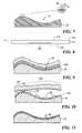
- surface 44presents a non-planar profile, e.g., undulations are present as hills 56 and troughs 57 . The undulations make problematic controlling thicknesses t 1 and t 2 .
- undulationsmake difficult ensuring that thickness t 1 is substantially equal over the area of formation 150 and thickness t 2 is substantially equal over the area of formation 150 .
- formation 150is formed in which regions over which thickness t 1 varies and thickness t 2 varies.
- features in region 58have a height thickness t′ 1 ⁇ t′ 1 and a residual thickness t′ 2 ⁇ t′ 2 , where ⁇ t′ 1 and ⁇ t′ 2 results from the variation in thickness t′ 1 and t′ 2 , respectively, due to the curvature of surface 44 in superimposition with region 58 .
- features in region 60have a height thickness t′′ 1 ⁇ t′′ 1 and a residual thickness t′′ 2 ⁇ t′′ 2 , where ⁇ t′′ 1 and ⁇ t′′ 2 correspond to the variation in thicknesses t′′ 1 and t′′ 2 , respectively, due to the curvature of surface 44 in superimposition with region 60 .
- etching of formation 150would occur until a break-through in region 60 occurs. This would cause substantially all of the features of region 58 to be removed. As a result, large regions of substrate 42 would remain unpatterned, due, inter alia, to the absence of masking material.
- template 114including a mold 136 , is made so as to conform to surface 44 .
- mold 136may conform in response to the presence of undulations, thereby minimizing variations among thickness t 1 and variations among thickness t 2 over the area of formation 50 .
- template 114is fabricated from a relatively thin sheet of fused silica having a thickness 113 , measured from opposed sides 115 and 116 , up to approximately 1.5 millimeters, with of approximately 0.7 being preferred.
- an area of template 114is approximately 4,225 square millimeters.
- the area of mold 136may be any desired, e.g., from 625 square millimeters to be extensive with the area of substrate 42 .
- the conformableness of template 114affords mold 136 the functionality so that control of thicknesses t 1 and t 2 may be achieved in the face of undulations.
- mold 136contacts imprinting material so that formation 250 may be formed.
- Formation 250has a first surface 252 that rests against substrate 42 and has a profile matching the profile of the surface 44 of substrate 42 in the presence of undulations.
- a difficulty presented by flexible mold 236results from the generation of capillary forces between mold 136 and the polymerizable material in droplets 46 .
- capillary forces between mold 136 and the polymerizable materialare generated.
- capillary forcesare substantially absent in the remaining sub-section of the polymerizable material, e.g., droplets in regions 160 and 161 .
- fluid pressureis applied to side 115 to deform template 114 and, therefore, mold 136 so that the same contacts droplets 46 in regions 160 and 161 .
- thickness t 1is within a specified tolerance ⁇ t 1 , referred to as being substantially uniform.
- thickness t 2is substantially uniform in that the same is within a specified tolerance ⁇ t 2 .
- the toleranceresults from the distortion in the features that result from the mold 136 conforming to surface 44 . It was determined, however, that by maintaining ⁇ t 1 and ⁇ t 2 to be less than or equal to 5 nanometers over a 25 millimeter area that the distortions that result from the conformableness of mold 136 are acceptable. Specifically, after a break-through-etch of formation 250 , regions 162 over the entire area of substrate 42 are exposed.
- recessions 164thereafter, patterning of the entire surface of substrate may occur, shown as recessions 164 .
- the entire substrate 42may be patterned, thereby overcoming the problems associated with thickness t 1 having, as well as thickness t 2 , varying, over an area of substrate 42 to be patterned.
- template 114is shown having a mold 136 with protrusions lying in a common plane P along with surface 116 , other templates may be employed.
- template 214may include a mesa 235 that embodies mold 236 .
- a height, h, of mesa 235is approximately 15 micrometers, as measured from surface 216 to a top surface of a protrusion 240 .
- template 314is substantially identical to template 114 , excepting that mold 336 is surrounded by an entrainment channel 337 .
- Entrainment channel 337extends further from side 316 than recessions 338 .
- template 414shown in FIG. 15 , is substantially identical to template 114 , shown in FIG. 8 , excepting that regions of side 416 lying outside of mold 436 are coplanar with recessions 438 .
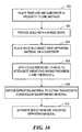
- template 214 and substrate 42are placed in proximity to one another, e.g., within one millimeter, at step 500 .
- template 214is bowed so that side 216 facing substrate 42 and, therefore, mold 236 , both have a convex shape, defining a bowed template.
- a neutral axis, N, of mold 236is bowed so that a central portion moves 350-400 micrometers away from neutral axis N so as to have a curved shape.
- the relative distance between the bowed template and substrate 42is reduced so that the bowed mold 236 is placed in contact with one or more of droplets 46 of imprinting material and subsequently conforms to the shape of the imprinting material disposed between mold 236 and substrate 42 under compression therebetween.
- mold 236is centered with respect to substrate 42 before contacting the imprinting material.
- a central portion 233 of mold 236is centered with respect to the area of substrate 42 that is to be patterned. In this example, nearly an entire surface 44 of substrate 44 is to be patterned.
- the dimension of the area of substrate 42 to be patternedis defined by the thicknesses of formation 250 and the aggregate volume of polymerizable material in droplets 46 .
- the area of mold 236may be greater, less than or equal to the area of substrate 42 .
- central portion 233 of mold 236contacts the center of the area (not shown) with the remaining portions of the imprinting area being subsequently contacted by the non-central portions of mold 236 .
- fluid pressureis applied to side 115 to attenuate, if not abrogate, variations among thickness t 1 of the area of formation 150 and variations among thickness t 2 over the area of formation 150 .
- side 115is subjected to a sufficient magnitude of fluid pressure to compress imprinting material between mold 236 and substrate 42 to the state whereby the imprinting material can no longer undergo compression.
- the imprinting materialdemonstrates visco-elastic properties in that the same behaves as a solid. Further, in the visco-elastic state the imprinting material conforms fully with surface 44 so that a side of the imprinting material facing mold 236 has the same shape as surface 44 .
- Mold 236is established to be more compliant than the imprinting material in a visco-elastic state and, therefore, fully conforms to the shape of the side of the imprinting material facing mold 236 .
- imprinting materialis exposed to actinic radiation to solidify the same so as to conform to a shape of the mold 236 and surface 44 of substrate 42 .
- mold 236is separated from the solidified imprinting material.
- a chuck body 520is adapted to retain template 214 employing vacuum techniques.
- chuck body 520includes first 522 and second 524 opposed sides.
- a side, or edge, surface 526extends between first side 520 and second side 524 .
- First side 522includes a first recess 532 and a second recess 534 , spaced-apart from first recess 532 , defining first 536 and second 538 spaced-apart support regions.
- First support region 536cinctures second support region 538 and the first 532 and second 534 recesses.
- Second support region 538cinctures second recess 534 .
- a portion 540 of chuck body 520 in superimposition with second recess 534is transmissive to energy having a predetermined wavelength, such as the wavelength of actinic energy employed to solidify the polymerizable material mentioned above.
- portion 540is made from a thin layer of material that is transmissive with respect to broad band ultraviolet energy, e.g., glass.
- the material from which portion 540 is mademay depend upon the wavelength of energy produced by source 26 , shown in FIG. 1 .
- portion 540extends from second side 524 and terminates proximate to second recess 534 and should define an area at least as large as an area of mold 236 so that mold 236 is in superimposition therewith.
- Formed in chuck body 520are one or more throughways, shown as 542 and 544 .
- One of the throughways, such as throughway 542places first recess 532 in fluid communication with side surface 526 .
- the remaining throughways, such as throughway 542places second recess 532 in fluid communication with side surface 526 .
- throughway 542may extend between second side 524 and first recess 532 , as well.
- throughway 544may extend between second side 524 and second recess 534 . What is desired is that throughways 542 and 544 facilitate placing recesses 532 and 534 , respectively, in fluid communication with a pressure control system, such a pump system 546 .
- Pump system 546may include one or more pumps to control the pressure proximate to recesses 532 and 534 , independently of one another. Specifically, when mounted to chuck body 520 , template 136 rests against first 536 and second 538 support regions, covering first 532 and second 534 recesses. First recess 532 and a portion 548 of template 136 in superimposition therewith define a first chamber 550 . Second recess 534 and a portion 552 of template 136 in superimposition therewith define a second chamber 554 . Pump system 546 operates to control a pressure in first 550 and second 554 chambers.
- the pressureis established in first chamber 550 to maintain the position of the template 214 with the chuck body 520 and reduce, if not avoid, separation of template 214 from chuck body 520 under force of gravity g .
- the pressure in second chamber 554may differ from the pressure in first chamber 548 to reduce, inter alia, distortions in the pattern generated by template 214 during imprinting, by modulating a shape of template 214 .
- pump system 546may apply a positive pressure in chamber 554 for the reasons discussed above. Pump system 546 is operated under control of processor 32 , shown in FIG. 1 .
- template 214is coupled to imprint head 20 via coupling of chuck body 520 to a flexure 556 that is coupled to an orientation system 558 .
- Orientation system 558moves template 214 .
- Flexure 556is disclosed and claimed in U.S. patent application Ser. No. 11/142,838, filed Jun. 1, 2005, entitled “Compliant Device for Nano-Scale Manufacturing”, which is assigned to the assignee of the present invention, and is incorporated by reference herein.
- Orientation system 558is disclosed in U.S. patent application Ser. No. 11/142,825, filed Jun. 1, 2005 entitled “Method and System to Control Movement of a Body for Nano-Scale Manufacturing,” which is assigned to the assignee of the present invention and incorporated by reference herein.
- orientation system 558is shown having an inner frame 560 disposed proximate to an outer frame 562 , and flexure ring 564 , discussed more fully below.
- Body 520is coupled to orientation system 558 through flexure 556 .
- body 520is connected to flexure 556 , using any suitable means, such as threaded fasteners (not shown) located at the four corners of body 520 connecting to four corners of flexure 556 closest to the four corners of body 520 .
- Four corners 566 of flexure 556 that are closest to a surface 568 of inner frame 560are connected thereto using any suitable means, such as threaded fasteners, not shown.
- Inner frame 560has a central throughway 570
- outer frame 562has a central opening 572 in superimposition with central throughway 570
- Flexure ring 564has an annular shape, e.g., circular or elliptical, and is coupled to inner frame 560 and outer frame 562 and lies outside of both central throughway 570 and central opening 572 .
- flexure ring 564is coupled to inner frame 560 at regions 574 , 576 and 578 , and outer frame 562 at regions 580 , 582 and 584 using any suitable means, such as threaded fasteners (not shown).
- Region 580is disposed between regions 574 and 576 and disposed equidistant therefrom; region 582 is disposed between regions 576 and 58 and disposed equidistant therefrom; and region 584 is disposed between regions 574 and 58 and disposed equidistant therefrom.
- flexure ring 564surrounds flexure 556 , body 520 , and template 214 and fixedly attaches inner frame 560 to outer frame 562 .
- orientation system 558 and flexure 556may be formed from any suitable material, e.g., aluminum, stainless steel and the like. Additionally, flexure 556 may be coupled to orientation system 558 using any suitable means. In the present example, flexure 556 is coupled to surface 45 employing threaded fasteners (not shown) located at the four corners 586 .
- system 558is configured to control movement of template 214 and to place the same in a desired spatial relationship with respect to a reference surface, such as substrate 42 disposed on stage 11 .
- a plurality of actuators 588 , 590 and 592are connected between outer frame 562 and inner frame 560 so as to be spaced about orientation system 558 .
- Each of actuators 588 , 590 and 592has a first end 594 and a second end 596 .
- First end 594faces outer frame 562
- second end 596faces away from outer frame 562 .
- actuators 588 , 590 and 592tilt inner frame 560 with respect to outer frame 562 by facilitating translational motion of inner frame 560 along three axes Z 1 , Z 2 , and Z 3 .
- Orientation system 558may provide a range of motion of approximately ⁇ 1.2 mm about axes Z 1 , Z 2 , and Z 3 .
- actuators 588 , 590 and 592cause inner frame 560 to impart angular motion to both flexure 556 and, therefore, template 214 and body 520 , about one or more of a plurality of axes T 1 , T 2 and T 3 .
- angular motion about tilt axis T 2occurs in a first direction.
- angular motion about tilt axis T 2occurs in a second direction opposite to the first direction.
- angular movement about axis T 1may occur by varying the distance between inner frame 560 and outer frame 562 by movement of inner frame 560 along axes Z 1 and Z 2 in the same direction and magnitude while moving of the inner frame 560 along axis Z 3 in a direction opposite and twice to the movement along axes Z 1 and Z 2 .
- angular movement about axis T 3may occur by varying the distance between inner frame 560 and outer frame 562 by movement of inner frame 560 along axes Z 1 and Z 3 in the same direction and magnitude while moving of inner frame 560 along axis Z 2 in direction opposite and twice to the movement along axes Z 1 and Z 3 .
- Actuators 588 , 590 and 592may have a maximum operational force of ⁇ 200 N.
- Orientation System 558may provide a range of motion of approximately ⁇ 0.15° about axes T 1 , T 2 , and T 3 .
- Actuators 588 , 590 and 592are selected to minimize mechanical parts and, therefore, minimize uneven mechanical compliance, as well as friction, which may cause particulates.
- Examples of actuators 588 , 590 and 592include voice coil actuators, piezo actuators, and linear actuators.
- An exemplary embodiment for actuators 588 , 590 and 592is available from BEI Technologies of Sylmar, Calif. under the trade name LA24-20-000A and are coupled to inner frame 560 using any suitable means, e.g., threaded fasteners.
- actuators 588 , 590 and 592are coupled between inner frame 560 and outer frame 562 so as to be symmetrically disposed thereabout and lie outside of central throughway 570 and central opening 572 . With this configuration an unobstructed throughway between outer frame 562 to flexure 556 is configured. Additionally, the symmetrical arrangement minimizes dynamic vibration and uneven thermal drift, thereby providing fine-motion correction of inner frame 560 .
- the combination of the inner frame 560 , outer frame 562 , flexure ring 564 and actuators 588 , 590 and 592provides angular motion of flexure 556 and, therefore, body 520 and template 214 about tilt axes T 1 , T 2 and T 3 . It is desired, however, that translational motion be imparted to template 214 along axes that lie in a plane extending transversely, if not orthogonally, to axes Z 1 , Z 2 , and Z 3 .
- flexure 556with the functionality to impart angular motion upon template 214 about one or more of a plurality of compliance axes, shown as C 1 and C 2 , which are spaced-part from tilt axes T 1 , T 2 and T 3 and exist on the surface of the template when the template, the template chuck, and the compliant device are assembled.
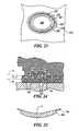
- Another embodiment of the present inventionfacilitates separation of mold 236 from the solidified imprinting material which forms, for example, formation 50 . This is based upon the finding that localizing initial separation to a relatively small area of the interface between mold 236 and the solidified imprinting material reduces the magnitude of upwardly forces imparted upon mold 236 by orientation system 558 necessary to achieve separation. A desirable result is that the probability of separation between substrate 42 and stage 11 is reduced.
- Imprint head 20applies a sufficient force to overcome the forces of attraction between mold 236 and formation 50 .
- the force required to separate mold 236 from formation 50is often much greater than the force of attraction between substrate 42 and stage 11 , e.g., a vacuum or electrostatic force of attraction between substrate 42 and stage 11 . Therefore, it is desirable to reduce the force applied to template 214 necessary to achieve separation of mold 236 from formation 50 . Specifically, it is desirable to ensure that the upwardly force required to separate template 114 from formation 50 is less than the downwardly applied by stage 11 to substrate 42 to maintain the same thereupon.
- the upwardly force required to separate template 214 from formation 50is reduced by creating localized separation between mold 236 and formation 50 at a region proximate to a periphery of mold 236 .
- mold 236will have a maximum area to ensure that a perimeter 237 thereof is spaced-apart from an edge 222 of substrate 42 approximately 1 millimeter, shown as distance R.
- Localized separationis obtained by initiating separation of mold 236 from the solidified imprinting material employing pump system 546 pressurizing chamber 554 to approximately 20 kPa. This distorts the shape of a region 217 of template 214 that surrounds mold 236 .
- a first portion 219 of the surface template 214 in region 217is displaced downwardly away from a neutral position N P toward substrate 42 , with the nadir of portion 219 being approximately 1 micrometer below surface 43 of substrate 42 .
- the distortion afforded to template 214 by pump system 546should be sufficient to allow nadir portion 219 to extend from the neutral position N P a magnitude that is greater than the thickness t 1 , shown in FIG. 3 , and height h, shown in FIG. 13 .
- a second portion 220 of the surface of template 214moves upwardly away from substrate 42 , with an apex thereof being spaced-apart from surface 43 approximately fifteen micrometers.
- the Young's modulus associated with template 214results in a returning force F R to facilitate returning region 217 to neutral position N P , wherein undulations shown as nadir portion 219 and second portion are attenuated to form arcuate surface 224 .
- the returning force F Rresults from the material of template 214 undergoing movement to return to a reduced-stressed and/or reduced-strained state.
- the returning force F Rcauses an area 221 of mold 236 proximate to region 217 to separate from substrate 42 , while segment 227 functions to press substrate 42 downwardly against stage 11 , firmly securing the same together.
- separation mold 236 from formation 50occurs by cantilevering template 214 with respect to substrate 42 .
- portion 227contacts edge 222 of substrate 42 holding the same against stage 11 , which reduces the upwardly force on template 214 required to separate mold 236 from substrate and prevents substrate 42 from separating from stage 11 . It can be said, therefore, that returning force F R reduces the magnitude of the upwardly forces imparted upon mold 236 by orientation system 558 that are necessary to achieve separation.
- returning force F Rmust be greater than the adhering force between area 221 and formation 50 .
- the returning force F Rresults in an oblique angle ⁇ being formed with respect to formation 50 , measured for example, between a plane P 2 in which nadir surfaces 138 of recessions 38 lie and a plane P 3 in which nadir surfaces 154 of recessed regions 54 lie.
- the back pressure and returning force F R coupled with the angle ⁇causes template 214 and, therefore, mold 236 , to have an arcuate shape in which region 221 is further from formation 50 than regions of mold 236 disposed remotely therefrom, center portions of mold 236 located proximate to center axis A.
- the angle ⁇will be on the order of micro-radians so that shearing of features in solidified layer 50 is on the order of pico-meters.
- the remaining portions of mold 236 are separated from formation 50may be controlled by operation of actuators 588 , 590 and 592 , shown in FIG. 19 .
- mold 236is separated from formation so that the last portions thereof proximate to region 221 are separated from formation 50 before regions proximate to center axis A.
- regions of mold 236 that are radially symmetrically disposed about axis Aare sequentially separated from formation 50 , e.g., region 221 separates then region 223 , then region 225 and etc. It should be understood, however, that regions 221 , 223 and 225 are radially symmetrically disposed about axis A, due to the shape of mold 236 . It is entirely possible that mold 236 have a rectangular or square shape.
- actuators 588 , 590 and 592may be operated so as to produce a peeling separation of mold 236 from formation 50 . This may be achieved by moving mold 236 about on of tilt axes T 1 , T 2 and T 3 .
- FIGS. 21 and 22another manner to achieve localized separation of template 214 would include forming arcuate surface 224 of template that is proximate to mold 236 .
- pump system 546would create a pressure in pressurizing chamber 554 sufficient to bow arcuate surface 224 and provide the same with a substantially constant radius of curvature.
- the returning force F Rwould induce localized separation between mold 236 and formation 50 proximate to region 221 , as discussed above.
- mold 236may be separated from formation 50 employing the techniques discussed above.
- Forming contoured surfaceis particularly advantageous were mold 236 sized so as to be much smaller than the area of substrate 42 , e.g., were mold 236 to have an area of 625 square millimeters, cantilevering would not occur.
Landscapes
- Engineering & Computer Science (AREA)
- Chemical & Material Sciences (AREA)
- Nanotechnology (AREA)
- Physics & Mathematics (AREA)
- General Physics & Mathematics (AREA)
- Crystallography & Structural Chemistry (AREA)
- Mathematical Physics (AREA)
- Theoretical Computer Science (AREA)
- Condensed Matter Physics & Semiconductors (AREA)
- Manufacturing & Machinery (AREA)
- Shaping Of Tube Ends By Bending Or Straightening (AREA)
- Moulds For Moulding Plastics Or The Like (AREA)
Abstract
Description
Claims (22)
Priority Applications (11)
| Application Number | Priority Date | Filing Date | Title |
|---|---|---|---|
| US11/292,568US7803308B2 (en) | 2005-12-01 | 2005-12-01 | Technique for separating a mold from solidified imprinting material |
| US11/303,777US7906058B2 (en) | 2005-12-01 | 2005-12-16 | Bifurcated contact printing technique |
| EP06804074AEP1954472A4 (en) | 2005-12-01 | 2006-09-22 | Technique for separating a mold from solidified imprinting material |
| KR1020087012782AKR101340922B1 (en) | 2005-12-01 | 2006-09-22 | Technique for separating a mold from solidified imprinting material |
| EP11186734AEP2413189A1 (en) | 2005-12-01 | 2006-09-22 | A method for spreading a conformable material between a substrate and a template |
| KR1020137014437AKR101375132B1 (en) | 2005-12-01 | 2006-09-22 | Technique for separating a mold from solidified imprinting material |
| PCT/US2006/037109WO2007064386A1 (en) | 2005-12-01 | 2006-09-22 | Technique for separating a mold from solidified imprinting material |
| JP2008543272AJP5236484B2 (en) | 2005-12-01 | 2006-09-22 | Method for separating a mold from a solidified imprinting material |
| CNA2006800441718ACN101316693A (en) | 2005-12-01 | 2006-09-22 | Technique for separating a mold from solidified imprinting material |
| TW095137688ATWI310730B (en) | 2005-12-01 | 2006-10-13 | Technique for separating a mold from solidified imprinting material |
| JP2012016219AJP5543502B2 (en) | 2005-12-01 | 2012-01-30 | Method for separating a mold from a solidified imprinting material |
Applications Claiming Priority (1)
| Application Number | Priority Date | Filing Date | Title |
|---|---|---|---|
| US11/292,568US7803308B2 (en) | 2005-12-01 | 2005-12-01 | Technique for separating a mold from solidified imprinting material |
Related Child Applications (1)
| Application Number | Title | Priority Date | Filing Date |
|---|---|---|---|
| US11/303,777DivisionUS7906058B2 (en) | 2005-12-01 | 2005-12-16 | Bifurcated contact printing technique |
Publications (2)
| Publication Number | Publication Date |
|---|---|
| US20070126156A1 US20070126156A1 (en) | 2007-06-07 |
| US7803308B2true US7803308B2 (en) | 2010-09-28 |
Family
ID=38117903
Family Applications (1)
| Application Number | Title | Priority Date | Filing Date |
|---|---|---|---|
| US11/292,568Active2027-08-12US7803308B2 (en) | 2005-12-01 | 2005-12-01 | Technique for separating a mold from solidified imprinting material |
Country Status (2)
| Country | Link |
|---|---|
| US (1) | US7803308B2 (en) |
| CN (1) | CN101316693A (en) |
Cited By (12)
| Publication number | Priority date | Publication date | Assignee | Title |
|---|---|---|---|---|
| US20100219401A1 (en)* | 2007-01-31 | 2010-09-02 | Donal Bradley | Deposition of Organic Layers |
| US20100237042A1 (en)* | 2009-03-23 | 2010-09-23 | Intevac, Inc. | Process for optimization of island to trench ratio in patterned media |
| US20100295028A1 (en)* | 2007-10-18 | 2010-11-25 | Novalia Ltd | Method of Fabricating an Electronic Device |
| US20100301508A1 (en)* | 2009-06-02 | 2010-12-02 | Hiroshi Tokue | Method for forming an imprint pattern |
| US20110084417A1 (en)* | 2009-10-08 | 2011-04-14 | Molecular Imprints, Inc. | Large area linear array nanoimprinting |
| US20120007276A1 (en)* | 2010-07-07 | 2012-01-12 | Katsutoshi Kobayashi | Imprint template, method for manufacturing imprint template, and pattern formation method |
| US20130187309A1 (en)* | 2012-01-20 | 2013-07-25 | Samsung Electronics Co., Ltd. | Stamp, method of fabricating the stamp, and imprint method using the same |
| US20170023857A1 (en)* | 2014-06-09 | 2017-01-26 | Canon Kabushiki Kaisha | Imprint apparatus and method of manufacturing article |
| US9798231B2 (en) | 2012-02-07 | 2017-10-24 | Canon Kabushiki Kaisha | Imprint apparatus and method of manufacturing article |
| US9811671B1 (en) | 2000-05-24 | 2017-11-07 | Copilot Ventures Fund Iii Llc | Authentication method and system |
| US9846814B1 (en) | 2008-04-23 | 2017-12-19 | Copilot Ventures Fund Iii Llc | Authentication method and system |
| US10018909B2 (en) | 2012-02-07 | 2018-07-10 | Canon Kabushiki Kaisha | Imprint apparatus and method of manufacturing article |
Families Citing this family (14)
| Publication number | Priority date | Publication date | Assignee | Title |
|---|---|---|---|---|
| US7906058B2 (en) | 2005-12-01 | 2011-03-15 | Molecular Imprints, Inc. | Bifurcated contact printing technique |
| US7670530B2 (en) | 2006-01-20 | 2010-03-02 | Molecular Imprints, Inc. | Patterning substrates employing multiple chucks |
| MY144847A (en) | 2005-12-08 | 2011-11-30 | Molecular Imprints Inc | Method and system for double-sided patterning of substrates |
| US8850980B2 (en) | 2006-04-03 | 2014-10-07 | Canon Nanotechnologies, Inc. | Tessellated patterns in imprint lithography |
| US20100096775A1 (en)* | 2008-10-16 | 2010-04-22 | Koh Teng Hwee | Mold imprinting |
| US20100096470A1 (en)* | 2008-10-17 | 2010-04-22 | Molecular Imprints, Inc. | Drop volume reduction |
| US8075299B2 (en)* | 2008-10-21 | 2011-12-13 | Molecular Imprints, Inc. | Reduction of stress during template separation |
| US8652393B2 (en) | 2008-10-24 | 2014-02-18 | Molecular Imprints, Inc. | Strain and kinetics control during separation phase of imprint process |
| US8309008B2 (en)* | 2008-10-30 | 2012-11-13 | Molecular Imprints, Inc. | Separation in an imprint lithography process |
| CN102349131A (en)* | 2009-03-12 | 2012-02-08 | 应用材料公司 | Large area dissolvable template lithography |
| EP2564271B1 (en) | 2010-04-27 | 2015-12-16 | Canon Nanotechnologies, Inc. | Separation control substrate/template for nanoimprint lithography |
| TW201501175A (en)* | 2013-06-19 | 2015-01-01 | Nanocrystal Asia Inc | Method for strengthening semiconductor manufacturing tools |
| US10620532B2 (en)* | 2014-11-11 | 2020-04-14 | Canon Kabushiki Kaisha | Imprint method, imprint apparatus, mold, and article manufacturing method |
| TWI672212B (en)* | 2016-08-25 | 2019-09-21 | 國立成功大學 | Nano imprinting assembly and imprinting method thereof |
Citations (233)
| Publication number | Priority date | Publication date | Assignee | Title |
|---|---|---|---|---|
| US1236304A (en) | 1917-02-03 | 1917-08-07 | Riley L Howell | Cushioned hand-stamp. |
| US2124711A (en)* | 1937-06-25 | 1938-07-26 | George S Rowell | Method and apparatus for reproducing images on curved surfaces |
| US2201302A (en) | 1938-11-30 | 1940-05-21 | Westinghouse Electric & Mfg Co | Printing device |
| US3503538A (en) | 1966-11-29 | 1970-03-31 | Bp Chem Int Ltd | Metering process and apparatus |
| US3868901A (en) | 1972-05-22 | 1975-03-04 | Interspace Corp | Apparatus for mechanical contact in printing on ceramic tableware |
| US4022855A (en) | 1975-03-17 | 1977-05-10 | Eastman Kodak Company | Method for making a plastic optical element having a gradient index of refraction |
| US4070116A (en) | 1975-06-23 | 1978-01-24 | International Business Machines Corporation | Gap measuring device for defining the distance between two or more surfaces |
| US4208240A (en) | 1979-01-26 | 1980-06-17 | Gould Inc. | Method and apparatus for controlling plasma etching |
| US4364971A (en) | 1980-06-18 | 1982-12-21 | Felix Schoeller, Jr. Gmbh & Co. | Waterproof photographic paper and method of producing same |
| US4440804A (en) | 1982-08-02 | 1984-04-03 | Fairchild Camera & Instrument Corporation | Lift-off process for fabricating self-aligned contacts |
| US4512848A (en) | 1984-02-06 | 1985-04-23 | Exxon Research And Engineering Co. | Procedure for fabrication of microstructures over large areas using physical replication |
| US4521445A (en) | 1982-09-07 | 1985-06-04 | Energy Sciences, Inc. | Method and apparatus for electron curing on a cooled drum |
| US4552832A (en) | 1982-03-06 | 1985-11-12 | Braun Aktiengesellschaft | Shear foil having protrusions on its skin-contacting surface thereof |
| US4576900A (en) | 1981-10-09 | 1986-03-18 | Amdahl Corporation | Integrated circuit multilevel interconnect system and method |
| US4637904A (en) | 1983-11-14 | 1987-01-20 | Rohm And Haas Company | Process for molding a polymeric layer onto a substrate |
| US4676868A (en) | 1986-04-23 | 1987-06-30 | Fairchild Semiconductor Corporation | Method for planarizing semiconductor substrates |
| US4707218A (en) | 1986-10-28 | 1987-11-17 | International Business Machines Corporation | Lithographic image size reduction |
| US4731155A (en) | 1987-04-15 | 1988-03-15 | General Electric Company | Process for forming a lithographic mask |
| US4737425A (en) | 1986-06-10 | 1988-04-12 | International Business Machines Corporation | Patterned resist and process |
| US4846931A (en) | 1988-03-29 | 1989-07-11 | Bell Communications Research, Inc. | Method for lifting-off epitaxial films |
| US4848911A (en) | 1986-06-11 | 1989-07-18 | Kabushiki Kaisha Toshiba | Method for aligning first and second objects, relative to each other, and apparatus for practicing this method |
| US4857477A (en) | 1986-09-18 | 1989-08-15 | Oki Electric Industry Co., Ltd. | Process for fabricating a semiconductor device |
| US4862019A (en) | 1988-04-20 | 1989-08-29 | Texas Instruments Incorporated | Single-level poly programmable bit circuit |
| US4866307A (en) | 1988-04-20 | 1989-09-12 | Texas Instruments Incorporated | Integrated programmable bit circuit using single-level poly construction |
| US4883561A (en) | 1988-03-29 | 1989-11-28 | Bell Communications Research, Inc. | Lift-off and subsequent bonding of epitaxial films |
| US4908298A (en) | 1985-03-19 | 1990-03-13 | International Business Machines Corporation | Method of creating patterned multilayer films for use in production of semiconductor circuits and systems |
| US4909151A (en) | 1986-11-10 | 1990-03-20 | Matsushita Electric Industrial Co., Ltd. | Method of forming an ink image and printing the formed image |
| US4919748A (en) | 1989-06-30 | 1990-04-24 | At&T Bell Laboratories | Method for tapered etching |
| US4921778A (en) | 1988-07-29 | 1990-05-01 | Shipley Company Inc. | Photoresist pattern fabrication employing chemically amplified metalized material |
| US4932358A (en) | 1989-05-18 | 1990-06-12 | Genus, Inc. | Perimeter wafer seal |
| US4936465A (en) | 1987-12-07 | 1990-06-26 | Zoeld Tibor | Method and apparatus for fast, reliable, and environmentally safe dispensing of fluids, gases and individual particles of a suspension through pressure control at well defined parts of a closed flow-through system |
| US4957663A (en) | 1986-02-13 | 1990-09-18 | U.S. Philips Corp. | Method of manufacturing optical components |
| US4959252A (en) | 1986-09-29 | 1990-09-25 | Rhone-Poulenc Chimie | Highly oriented thermotropic optical disc member |
| US4964945A (en) | 1988-12-09 | 1990-10-23 | Minnesota Mining And Manufacturing Company | Lift off patterning process on a flexible substrate |
| US4980316A (en) | 1988-07-20 | 1990-12-25 | Siemens Aktiengesellschaft | Method for producing a resist structure on a semiconductor |
| US5003062A (en) | 1990-04-19 | 1991-03-26 | Taiwan Semiconductor Manufacturing Co. | Semiconductor planarization process for submicron devices |
| US5028366A (en) | 1988-01-12 | 1991-07-02 | Air Products And Chemicals, Inc. | Water based mold release compositions for making molded polyurethane foam |
| US5028361A (en) | 1987-11-09 | 1991-07-02 | Takeo Fujimoto | Method for molding a photosensitive composition |
| US5053318A (en) | 1989-05-18 | 1991-10-01 | Shipley Company Inc. | Plasma processing with metal mask integration |
| US5073230A (en) | 1990-04-17 | 1991-12-17 | Arizona Board Of Regents Acting On Behalf Of Arizona State University | Means and methods of lifting and relocating an epitaxial device layer |
| US5110514A (en) | 1989-05-01 | 1992-05-05 | Soane Technologies, Inc. | Controlled casting of a shrinkable material |
| US5124089A (en) | 1986-12-25 | 1992-06-23 | Sony Corporation | Method of producing transmissive screens |
| US5126006A (en) | 1990-10-30 | 1992-06-30 | International Business Machines Corp. | Plural level chip masking |
| US5148037A (en) | 1988-09-09 | 1992-09-15 | Canon Kabushiki Kaisha | Position detecting method and apparatus |
| US5151754A (en) | 1989-10-06 | 1992-09-29 | Kabushiki Kaisha Toshiba | Method and an apparatus for measuring a displacement between two objects and a method and an apparatus for measuring a gap distance between two objects |
| FR2677043A1 (en) | 1991-05-29 | 1992-12-04 | Solems Sa | Process, device and apparatus for treating a substrate with a low-pressure plasma |
| US5212147A (en) | 1991-05-15 | 1993-05-18 | Hewlett-Packard Company | Method of forming a patterned in-situ high Tc superconductive film |
| US5232874A (en) | 1992-06-22 | 1993-08-03 | Micron Technology, Inc. | Method for producing a semiconductor wafer having shallow and deep buried contacts |
| US5240878A (en) | 1991-04-26 | 1993-08-31 | International Business Machines Corporation | Method for forming patterned films on a substrate |
| US5240550A (en) | 1990-09-21 | 1993-08-31 | U.S. Philips Corp. | Method of forming at least one groove in a substrate layer |
| US5244818A (en) | 1992-04-08 | 1993-09-14 | Georgia Tech Research Corporation | Processes for lift-off of thin film materials and for the fabrication of three dimensional integrated circuits |
| US5246880A (en) | 1992-04-27 | 1993-09-21 | Eastman Kodak Company | Method for creating substrate electrodes for flip chip and other applications |
| US5250472A (en) | 1992-09-03 | 1993-10-05 | Industrial Technology Research Institute | Spin-on-glass integration planarization having siloxane partial etchback and silicate processes |
| US5259926A (en) | 1991-09-24 | 1993-11-09 | Hitachi, Ltd. | Method of manufacturing a thin-film pattern on a substrate |
| US5277749A (en) | 1991-10-17 | 1994-01-11 | International Business Machines Corporation | Methods and apparatus for relieving stress and resisting stencil delamination when performing lift-off processes that utilize high stress metals and/or multiple evaporation steps |
| US5288436A (en) | 1990-11-06 | 1994-02-22 | Colloptics, Inc. | Methods of fabricating a collagen lenticule precursor for modifying the cornea |
| US5324683A (en) | 1993-06-02 | 1994-06-28 | Motorola, Inc. | Method of forming a semiconductor structure having an air region |
| US5328810A (en) | 1990-05-07 | 1994-07-12 | Micron Technology, Inc. | Method for reducing, by a factor or 2-N, the minimum masking pitch of a photolithographic process |
| US5330881A (en) | 1989-06-02 | 1994-07-19 | Digital Equipment Corp. | Microlithographic method for producing thick, vertically-walled photoresist patterns |
| US5357122A (en) | 1991-09-05 | 1994-10-18 | Sony Corporation | Three-dimensional optical-electronic integrated circuit device with raised sections |
| US5362606A (en) | 1989-10-18 | 1994-11-08 | Massachusetts Institute Of Technology | Positive resist pattern formation through focused ion beam exposure and surface barrier silylation |
| US5362940A (en) | 1990-11-09 | 1994-11-08 | Litel Instruments | Use of Fresnel zone plates for material processing |
| US5364222A (en) | 1992-02-05 | 1994-11-15 | Tokyo Electron Limited | Apparatus for processing wafer-shaped substrates |
| US5366851A (en) | 1991-07-23 | 1994-11-22 | At&T Bell Laboratories | Device fabrication process |
| US5371822A (en) | 1992-06-09 | 1994-12-06 | Digital Equipment Corporation | Method of packaging and assembling opto-electronic integrated circuits |
| US5374327A (en) | 1992-04-28 | 1994-12-20 | Tokyo Electron Limited | Plasma processing method |
| US5376810A (en) | 1992-06-26 | 1994-12-27 | California Institute Of Technology | Growth of delta-doped layers on silicon CCD/S for enhanced ultraviolet response |
| US5422295A (en) | 1992-12-10 | 1995-06-06 | Samsung Electronics Co., Ltd. | Method for forming a semiconductor memory device having a vertical multi-layered storage electrode |
| US5424549A (en) | 1991-12-20 | 1995-06-13 | Board Of Supervisors Of Louisiana State University And Agricultural And Mechanical College | Scanning systems for high resolution e-beam and X-ray lithography |
| US5425848A (en) | 1993-03-16 | 1995-06-20 | U.S. Philips Corporation | Method of providing a patterned relief of cured photoresist on a flat substrate surface and device for carrying out such a method |
| US5431777A (en) | 1992-09-17 | 1995-07-11 | International Business Machines Corporation | Methods and compositions for the selective etching of silicon |
| US5434107A (en) | 1994-01-28 | 1995-07-18 | Texas Instruments Incorporated | Method for planarization |
| US5445195A (en) | 1992-07-15 | 1995-08-29 | Kim; Dae S. | Automatic computer-controlled liquid dispenser |
| US5449117A (en) | 1993-10-04 | 1995-09-12 | Technical Concepts, L.P. | Apparatus and method for controllably dispensing drops of liquid |
| US5451435A (en) | 1990-06-18 | 1995-09-19 | At&T Corp. | Method for forming dielectric |
| US5453157A (en) | 1994-05-16 | 1995-09-26 | Texas Instruments Incorporated | Low temperature anisotropic ashing of resist for semiconductor fabrication |
| US5458520A (en) | 1994-12-13 | 1995-10-17 | International Business Machines Corporation | Method for producing planar field emission structure |
| US5468542A (en) | 1985-12-23 | 1995-11-21 | General Electric Company | Method for production of a coated substrate with controlled surface characteristics |
| US5480047A (en) | 1993-06-04 | 1996-01-02 | Sharp Kabushiki Kaisha | Method for forming a fine resist pattern |
| US5512131A (en) | 1993-10-04 | 1996-04-30 | President And Fellows Of Harvard College | Formation of microstamped patterns on surfaces and derivative articles |
| US5542605A (en) | 1994-04-07 | 1996-08-06 | Flow-Rite Controls, Ltd. | Automatic liquid dispenser |
| US5545367A (en) | 1992-04-15 | 1996-08-13 | Soane Technologies, Inc. | Rapid prototype three dimensional stereolithography |
| US5601641A (en) | 1992-07-21 | 1997-02-11 | Tse Industries, Inc. | Mold release composition with polybutadiene and method of coating a mold core |
| US5612068A (en) | 1994-03-14 | 1997-03-18 | Leybold Aktiengesellschaft | Apparatus for the transfer of substrates |
| US5628917A (en) | 1995-02-03 | 1997-05-13 | Cornell Research Foundation, Inc. | Masking process for fabricating ultra-high aspect ratio, wafer-free micro-opto-electromechanical structures |
| US5643364A (en) | 1994-11-30 | 1997-07-01 | Applied Materials, Inc. | Plasma chamber with fixed RF matching |
| US5654238A (en) | 1995-08-03 | 1997-08-05 | International Business Machines Corporation | Method for etching vertical contact holes without substrate damage caused by directional etching |
| EP0795016A1 (en) | 1994-12-22 | 1997-09-17 | Richard Collins | Vs ribozymes |
| US5669303A (en) | 1996-03-04 | 1997-09-23 | Motorola | Apparatus and method for stamping a surface |
| US5736424A (en) | 1987-02-27 | 1998-04-07 | Lucent Technologies Inc. | Device fabrication involving planarization |
| US5753014A (en) | 1993-11-12 | 1998-05-19 | Van Rijn; Cornelis Johannes Maria | Membrane filter and a method of manufacturing the same as well as a membrane |
| US5772905A (en) | 1995-11-15 | 1998-06-30 | Regents Of The University Of Minnesota | Nanoimprint lithography |
| US5776748A (en) | 1993-10-04 | 1998-07-07 | President And Fellows Of Harvard College | Method of formation of microstamped patterns on plates for adhesion of cells and other biological materials, devices and uses therefor |
| US5779799A (en) | 1996-06-21 | 1998-07-14 | Micron Technology, Inc. | Substrate coating apparatus |
| US5804474A (en) | 1996-04-10 | 1998-09-08 | Murata Manufacturing Co., Ltd. | Method for forming a V-shaped gate electrode in a semiconductor device, and the structure of the electrode |
| US5812629A (en) | 1997-04-30 | 1998-09-22 | Clauser; John F. | Ultrahigh resolution interferometric x-ray imaging |
| US5817579A (en) | 1997-04-09 | 1998-10-06 | Vanguard International Semiconductor Corporation | Two step plasma etch method for forming self aligned contact |
| US5820769A (en) | 1995-05-24 | 1998-10-13 | Regents Of The University Of Minnesota | Method for making magnetic storage having discrete elements with quantized magnetic moments |
| US5843363A (en) | 1995-03-31 | 1998-12-01 | Siemens Aktiengesellschaft | Ablation patterning of multi-layered structures |
| US5849209A (en) | 1995-03-31 | 1998-12-15 | Johnson & Johnson Vision Products, Inc. | Mold material made with additives |
| US5849222A (en) | 1995-09-29 | 1998-12-15 | Johnson & Johnson Vision Products, Inc. | Method for reducing lens hole defects in production of contact lens blanks |
| US5858580A (en) | 1997-09-17 | 1999-01-12 | Numerical Technologies, Inc. | Phase shifting circuit manufacture method and apparatus |
| US5888650A (en) | 1996-06-03 | 1999-03-30 | Minnesota Mining And Manufacturing Company | Temperature-responsive adhesive article |
| US5895263A (en) | 1996-12-19 | 1999-04-20 | International Business Machines Corporation | Process for manufacture of integrated circuit device |
| US5900160A (en) | 1993-10-04 | 1999-05-04 | President And Fellows Of Harvard College | Methods of etching articles via microcontact printing |
| US5907782A (en) | 1998-08-15 | 1999-05-25 | Acer Semiconductor Manufacturing Inc. | Method of forming a multiple fin-pillar capacitor for a high density dram cell |
| US5926690A (en) | 1997-05-28 | 1999-07-20 | Advanced Micro Devices, Inc. | Run-to-run control process for controlling critical dimensions |
| US5948570A (en) | 1995-05-26 | 1999-09-07 | Lucent Technologies Inc. | Process for dry lithographic etching |
| US5948470A (en) | 1997-04-28 | 1999-09-07 | Harrison; Christopher | Method of nanoscale patterning and products made thereby |
| US5974150A (en) | 1997-09-30 | 1999-10-26 | Tracer Detection Technology Corp. | System and method for authentication of goods |
| US5983906A (en) | 1997-01-24 | 1999-11-16 | Applied Materials, Inc. | Methods and apparatus for a cleaning process in a high temperature, corrosive, plasma environment |
| US6046056A (en) | 1996-06-28 | 2000-04-04 | Caliper Technologies Corporation | High throughput screening assay systems in microscale fluidic devices |
| US6048799A (en) | 1987-02-27 | 2000-04-11 | Lucent Technologies Inc. | Device fabrication involving surface planarization |
| US6067144A (en) | 1996-10-23 | 2000-05-23 | Kabushiki Kaisha Toshiba | LCD cell having two supporting gap members different in height |
| US6074827A (en) | 1996-07-30 | 2000-06-13 | Aclara Biosciences, Inc. | Microfluidic method for nucleic acid purification and processing |
| US6150680A (en) | 1998-03-05 | 2000-11-21 | Welch Allyn, Inc. | Field effect semiconductor device having dipole barrier |
| US6180239B1 (en) | 1993-10-04 | 2001-01-30 | President And Fellows Of Harvard College | Microcontact printing on surfaces and derivative articles |
| US6218316B1 (en) | 1998-10-22 | 2001-04-17 | Micron Technology, Inc. | Planarization of non-planar surfaces in device fabrication |
| US6242363B1 (en) | 1999-08-11 | 2001-06-05 | Adc Telecommunications, Inc. | Method of etching a wafer layer using a sacrificial wall to form vertical sidewall |
| US6245213B1 (en) | 1996-09-06 | 2001-06-12 | Obducat Ab | Method for anisotropic etching of structures in conducting materials |
| US6274294B1 (en) | 1999-02-03 | 2001-08-14 | Electroformed Stents, Inc. | Cylindrical photolithography exposure process and apparatus |
| US6309580B1 (en) | 1995-11-15 | 2001-10-30 | Regents Of The University Of Minnesota | Release surfaces, particularly for use in nanoimprint lithography |
| US6326627B1 (en) | 2000-08-02 | 2001-12-04 | Archimedes Technology Group, Inc. | Mass filtering sputtered ion source |
| US6329256B1 (en) | 1999-09-24 | 2001-12-11 | Advanced Micro Devices, Inc. | Self-aligned damascene gate formation with low gate resistance |
| US6334960B1 (en) | 1999-03-11 | 2002-01-01 | Board Of Regents, The University Of Texas System | Step and flash imprint lithography |
| US6337262B1 (en) | 2000-03-06 | 2002-01-08 | Chartered Semiconductor Manufacturing Ltd. | Self aligned T-top gate process integration |
| US6348999B1 (en) | 1995-05-10 | 2002-02-19 | Epigem Limited | Micro relief element and preparation thereof |
| US6355198B1 (en) | 1996-03-15 | 2002-03-12 | President And Fellows Of Harvard College | Method of forming articles including waveguides via capillary micromolding and microtransfer molding |
| US20020038916A1 (en) | 1998-12-23 | 2002-04-04 | 3M Innovative Properties Company | Method for precise molding and alignment of structures on a substrate using a stretchable mold |
| US20020042027A1 (en) | 1998-10-09 | 2002-04-11 | Chou Stephen Y. | Microscale patterning and articles formed thereby |
| US6376379B1 (en) | 2000-02-01 | 2002-04-23 | Chartered Semiconductor Manufacturing Ltd. | Method of hard mask patterning |
| US6383928B1 (en) | 1999-09-02 | 2002-05-07 | Texas Instruments Incorporated | Post copper CMP clean |
| US6387783B1 (en) | 1999-04-26 | 2002-05-14 | International Business Machines Corporation | Methods of T-gate fabrication using a hybrid resist |
| US6388253B1 (en) | 1999-06-29 | 2002-05-14 | Applied Materials, Inc. | Integrated critical dimension control for semiconductor device manufacturing |
| US6387330B1 (en) | 2000-04-12 | 2002-05-14 | George Steven Bova | Method and apparatus for storing and dispensing reagents |
| US6391217B2 (en) | 1999-12-23 | 2002-05-21 | University Of Massachusetts | Methods and apparatus for forming submicron patterns on films |
| US6391798B1 (en) | 1987-02-27 | 2002-05-21 | Agere Systems Guardian Corp. | Process for planarization a semiconductor substrate |
| US20020094496A1 (en) | 2000-07-17 | 2002-07-18 | Choi Byung J. | Method and system of automatic fluid dispensing for imprint lithography processes |
| US6423207B1 (en) | 1998-03-05 | 2002-07-23 | Obducat Ab | Method and apparatus for etching |
| US20020111036A1 (en) | 2001-02-12 | 2002-08-15 | Lam Research Corporation | Unique process chemistry for etching organic low-k materials |
| US20020110992A1 (en) | 2001-02-12 | 2002-08-15 | Lam Research Corporation | Use of hydrocarbon addition for the elimination of micromasking during etching |
| US20020132482A1 (en) | 2000-07-18 | 2002-09-19 | Chou Stephen Y. | Fluid pressure imprint lithography |
| US20020150398A1 (en) | 2000-08-21 | 2002-10-17 | Choi Byung J. | Flexure based macro motion translation stage |
| US20020168578A1 (en) | 1996-09-18 | 2002-11-14 | Numerical Technologies, Inc. | Phase shifting circuit manufacture method and apparatus |
| US20020170880A1 (en) | 2001-03-22 | 2002-11-21 | Yong Chen | Scanning probe based lithographic alignment |
| US6495907B1 (en) | 1994-09-30 | 2002-12-17 | Texas Instruments Incorporated | Conductor reticulation for improved device planarity |
| US20020191141A1 (en) | 2001-06-14 | 2002-12-19 | Bing-Jei Liao | Panel with a blocker for separating sealant and liquid crystal layer |
| US6498640B1 (en) | 1999-12-30 | 2002-12-24 | Koninklijke Philips Electronics N.V. | Method to measure alignment using latent image grating structures |
| US6503829B2 (en) | 2000-08-19 | 2003-01-07 | Samsung Electronics Co., Ltd. | Metal via contact of a semiconductor device and method for fabricating the same |
| US20030017424A1 (en)* | 2001-07-18 | 2003-01-23 | Miri Park | Method and apparatus for fabricating complex grating structures |
| US6514672B2 (en) | 1999-06-17 | 2003-02-04 | Taiwan Semiconductor Manufacturing Company | Dry development process for a bi-layer resist system |
| US20030025895A1 (en) | 2001-08-03 | 2003-02-06 | Michael Binnard | Apparatus and methods for detecting tool-induced shift in microlithography apparatus |
| US6518189B1 (en) | 1995-11-15 | 2003-02-11 | Regents Of The University Of Minnesota | Method and apparatus for high density nanostructures |
| US6517995B1 (en) | 1999-09-14 | 2003-02-11 | Massachusetts Institute Of Technology | Fabrication of finely featured devices by liquid embossing |
| US6517977B2 (en) | 2001-03-28 | 2003-02-11 | Motorola, Inc. | Lithographic template and method of formation and use |
| US6521536B1 (en) | 1999-01-11 | 2003-02-18 | Micron Technology, Inc. | Planarization process |
| US6534418B1 (en) | 2001-04-30 | 2003-03-18 | Advanced Micro Devices, Inc. | Use of silicon containing imaging layer to define sub-resolution gate structures |
| US6541360B1 (en) | 2001-04-30 | 2003-04-01 | Advanced Micro Devices, Inc. | Bi-layer trim etch process to form integrated circuit gate structures |
| US20030062334A1 (en) | 2001-09-25 | 2003-04-03 | Lee Hong Hie | Method for forming a micro-pattern on a substrate by using capillary force |
| US20030080471A1 (en) | 2001-10-29 | 2003-05-01 | Chou Stephen Y. | Lithographic method for molding pattern with nanoscale features |
| US20030081193A1 (en) | 2001-06-01 | 2003-05-01 | White Donald L. | Holder, system, and process for improving overlay in lithography |
| US20030092261A1 (en) | 2000-12-04 | 2003-05-15 | Fumio Kondo | Substrate processing method |
| US6565928B2 (en) | 1999-03-08 | 2003-05-20 | Tokyo Electron Limited | Film forming method and film forming apparatus |
| US6580172B2 (en) | 2001-03-02 | 2003-06-17 | Motorola, Inc. | Lithographic template and method of formation and use |
| US6586268B1 (en) | 1998-08-11 | 2003-07-01 | Valtion Teknillinen Tutkimuskeskus | Optoelectronic component and manufacturing method |
| US20030129542A1 (en) | 2001-10-31 | 2003-07-10 | Brewer Science, Inc. | Contact planarization materials that generate no volatile byproducts or residue during curing |
| US6593240B1 (en) | 2000-06-28 | 2003-07-15 | Infineon Technologies, North America Corp | Two step chemical mechanical polishing process |
| US20030137494A1 (en) | 2000-05-01 | 2003-07-24 | Tulbert David J. | Human-machine interface |
| US20030151714A1 (en) | 2002-01-08 | 2003-08-14 | Kabushiki Kaisha Toshiba | Liquid crystal display device |
| US6621960B2 (en) | 2002-01-24 | 2003-09-16 | Oplink Communications, Inc. | Method of fabricating multiple superimposed fiber Bragg gratings |
| US20030174435A1 (en) | 2002-03-18 | 2003-09-18 | International Business Machines Corporation | Method and apparatus for providing an aligned coil for an inductive head structure using a patterned seed layer |
| US6623579B1 (en) | 1999-11-02 | 2003-09-23 | Alien Technology Corporation | Methods and apparatus for fluidic self assembly |
| US20030179354A1 (en) | 1996-03-22 | 2003-09-25 | Nikon Corporation | Mask-holding apparatus for a light exposure apparatus and related scanning-exposure method |
| US6627544B2 (en) | 2001-05-22 | 2003-09-30 | Sharp Kabushiki Kaisha | Method of making a metal film pattern |
| US6629292B1 (en) | 2000-10-06 | 2003-09-30 | International Business Machines Corporation | Method for forming graphical images in semiconductor devices |
| US20030186140A1 (en) | 2001-06-27 | 2003-10-02 | Fries David P. | Maskless photolithography for using photoreactive agents |
| US20030184917A1 (en) | 2002-03-29 | 2003-10-02 | Ping-Wei Chang | Planarization in an encapsulation process for thin film surfaces |
| US6632742B2 (en) | 2001-04-18 | 2003-10-14 | Promos Technologies Inc. | Method for avoiding defects produced in the CMP process |
| US6635581B2 (en) | 2001-06-08 | 2003-10-21 | Au Optronics, Corp. | Method for forming a thin-film transistor |
| US20030197312A1 (en) | 2002-04-22 | 2003-10-23 | International Business Machines Corporation | Process of fabricating a precision microcontact printing stamp |
| US6646662B1 (en) | 1998-05-26 | 2003-11-11 | Seiko Epson Corporation | Patterning method, patterning apparatus, patterning template, and method for manufacturing the patterning template |
| US20030224116A1 (en) | 2002-05-30 | 2003-12-04 | Erli Chen | Non-conformal overcoat for nonometer-sized surface structure |
| US6665014B1 (en) | 1998-11-25 | 2003-12-16 | Intel Corporation | Microlens and photodetector |
| US20040022888A1 (en) | 2002-08-01 | 2004-02-05 | Sreenivasan Sidlgata V. | Alignment systems for imprint lithography |
| US20040021866A1 (en) | 2002-08-01 | 2004-02-05 | Watts Michael P.C. | Scatterometry alignment for imprint lithography |
| US20040029041A1 (en) | 2002-02-27 | 2004-02-12 | Brewer Science, Inc. | Novel planarization method for multi-layer lithography processing |
| US6696220B2 (en) | 2000-10-12 | 2004-02-24 | Board Of Regents, The University Of Texas System | Template for room temperature, low pressure micro-and nano-imprint lithography |
| US20040038552A1 (en) | 2002-08-23 | 2004-02-26 | Watts Michael P.C. | Method for fabricating bulbous-shaped vias |
| US20040036201A1 (en) | 2000-07-18 | 2004-02-26 | Princeton University | Methods and apparatus of field-induced pressure imprint lithography |
| WO2004016406A1 (en) | 2002-07-11 | 2004-02-26 | Molecular Imprints, Inc. | Imprint lithography processes and systems |
| US20040046288A1 (en) | 2000-07-18 | 2004-03-11 | Chou Stephen Y. | Laset assisted direct imprint lithography |
| US6716754B2 (en) | 2002-03-12 | 2004-04-06 | Micron Technology, Inc. | Methods of forming patterns and molds for semiconductor constructions |
| US20040065252A1 (en) | 2002-10-04 | 2004-04-08 | Sreenivasan Sidlgata V. | Method of forming a layer on a substrate to facilitate fabrication of metrology standards |
| US20040065976A1 (en) | 2002-10-04 | 2004-04-08 | Sreenivasan Sidlgata V. | Method and a mold to arrange features on a substrate to replicate features having minimal dimensional variability |
| US20040110856A1 (en) | 2002-12-04 | 2004-06-10 | Young Jung Gun | Polymer solution for nanoimprint lithography to reduce imprint temperature and pressure |
| US20040124566A1 (en) | 2002-07-11 | 2004-07-01 | Sreenivasan Sidlgata V. | Step and repeat imprint lithography processes |
| US20040131718A1 (en) | 2000-07-18 | 2004-07-08 | Princeton University | Lithographic apparatus for fluid pressure imprint lithography |
| US20040137734A1 (en) | 1995-11-15 | 2004-07-15 | Princeton University | Compositions and processes for nanoimprinting |
| US20040146792A1 (en) | 2002-12-13 | 2004-07-29 | Molecular Imprints, Inc. | Magnification correction employing out-of-plane distortion of a substrate |
| US20040156108A1 (en) | 2001-10-29 | 2004-08-12 | Chou Stephen Y. | Articles comprising nanoscale patterns with reduced edge roughness and methods of making same |
| US6776094B1 (en) | 1993-10-04 | 2004-08-17 | President & Fellows Of Harvard College | Kit For Microcontact Printing |
| US20040192041A1 (en) | 2003-03-27 | 2004-09-30 | Jun-Ho Jeong | UV nanoimprint lithography process using elementwise embossed stamp and selectively additive pressurization |
| US20040197843A1 (en) | 2001-07-25 | 2004-10-07 | Chou Stephen Y. | Nanochannel arrays and their preparation and use for high throughput macromolecular analysis |
| US20040201890A1 (en) | 2002-12-30 | 2004-10-14 | Ian Crosby | Microlens including wire-grid polarizer and methods of manufacture |
| US6805054B1 (en) | 2003-05-14 | 2004-10-19 | Molecular Imprints, Inc. | Method, system and holder for transferring templates during imprint lithography processes |
| US20040250945A1 (en) | 2003-06-10 | 2004-12-16 | Industrial Technology Research Institute | Method for and apparatus for bonding patterned imprint to a substrate by adhering means |
| US6833325B2 (en) | 2002-10-11 | 2004-12-21 | Lam Research Corporation | Method for plasma etching performance enhancement |
| US20050006343A1 (en) | 2003-07-09 | 2005-01-13 | Molecular Imprints, Inc. | Systems for magnification and distortion correction for imprint lithography processes |
| US6849558B2 (en) | 2002-05-22 | 2005-02-01 | The Board Of Trustees Of The Leland Stanford Junior University | Replication and transfer of microstructures and nanostructures |
| US20050037143A1 (en) | 2000-07-18 | 2005-02-17 | Chou Stephen Y. | Imprint lithography with improved monitoring and control and apparatus therefor |
| US20050056963A1 (en) | 2003-07-10 | 2005-03-17 | Mccutcheon Jeremy W. | Automated process and apparatus for planarization of topographical surfaces |
| US6870301B2 (en) | 1999-10-29 | 2005-03-22 | Board Of Regents, The University Of Texas System | Method of separating a template from a substrate during imprint lithography |
| US6879162B2 (en) | 2000-11-07 | 2005-04-12 | Sri International | System and method of micro-fluidic handling and dispensing using micro-nozzle structures |
| US6900881B2 (en) | 2002-07-11 | 2005-05-31 | Molecular Imprints, Inc. | Step and repeat imprint lithography systems |
| US6908861B2 (en) | 2002-07-11 | 2005-06-21 | Molecular Imprints, Inc. | Method for imprint lithography using an electric field |
| US6916584B2 (en) | 2002-08-01 | 2005-07-12 | Molecular Imprints, Inc. | Alignment methods for imprint lithography |
| US6916585B2 (en) | 2000-07-16 | 2005-07-12 | Board Of Regents, The University Of Texas Systems | Method of varying template dimensions to achieve alignment during imprint lithography |
| US6932934B2 (en) | 2002-07-11 | 2005-08-23 | Molecular Imprints, Inc. | Formation of discontinuous films during an imprint lithography process |
| US20050189676A1 (en) | 2004-02-27 | 2005-09-01 | Molecular Imprints, Inc. | Full-wafer or large area imprinting with multiple separated sub-fields for high throughput lithography |
| US6951173B1 (en) | 2003-05-14 | 2005-10-04 | Molecular Imprints, Inc. | Assembly and method for transferring imprint lithography templates |
| US6964793B2 (en) | 2002-05-16 | 2005-11-15 | Board Of Regents, The University Of Texas System | Method for fabricating nanoscale patterns in light curable compositions using an electric field |
| US20050284886A1 (en) | 2004-06-25 | 2005-12-29 | Cristian Penciu | Apparatus for mixing and dispensing fluids |
| US20060017876A1 (en) | 2004-07-23 | 2006-01-26 | Molecular Imprints, Inc. | Displays and method for fabricating displays |
| US20060113697A1 (en) | 2004-12-01 | 2006-06-01 | Molecular Imprints, Inc. | Eliminating printability of sub-resolution defects in imprint lithography |
| US20060131785A1 (en)* | 2004-12-16 | 2006-06-22 | Asml Holding N.V. | System and method for patterning both sides of a substrate utilizing imprint lithography |
| US20060172031A1 (en) | 2005-01-31 | 2006-08-03 | Molecular Imprints, Inc. | Chucking system for nano-manufacturing |
| US7105452B2 (en) | 2004-08-13 | 2006-09-12 | Molecular Imprints, Inc. | Method of planarizing a semiconductor substrate with an etching chemistry |
| US7128875B2 (en) | 1995-04-10 | 2006-10-31 | Cubicciotti Roger S | Signal processing devices comprising biological and bio-mimetic components |
| US7214624B2 (en) | 2003-11-14 | 2007-05-08 | Tdk Corporation | Resist pattern forming method, magnetic recording medium manufacturing method and magnetic head manufacturing method |
| US20070126150A1 (en) | 2005-12-01 | 2007-06-07 | Molecular Imprints, Inc. | Bifurcated contact printing technique |
| US20070132152A1 (en) | 2005-12-08 | 2007-06-14 | Molecular Imprints, Inc. | Method and System for Double-Sided Patterning of Substrates |
| US7244386B2 (en) | 2004-09-27 | 2007-07-17 | Molecular Imprints, Inc. | Method of compensating for a volumetric shrinkage of a material disposed upon a substrate to form a substantially planar structure therefrom |
| US20070170617A1 (en) | 2006-01-20 | 2007-07-26 | Molecular Imprints, Inc. | Patterning Substrates Employing Multiple Chucks |
- 2005
- 2005-12-01USUS11/292,568patent/US7803308B2/enactiveActive
- 2006
- 2006-09-22CNCNA2006800441718Apatent/CN101316693A/enactivePending
Patent Citations (257)
| Publication number | Priority date | Publication date | Assignee | Title |
|---|---|---|---|---|
| US1236304A (en) | 1917-02-03 | 1917-08-07 | Riley L Howell | Cushioned hand-stamp. |
| US2124711A (en)* | 1937-06-25 | 1938-07-26 | George S Rowell | Method and apparatus for reproducing images on curved surfaces |
| US2201302A (en) | 1938-11-30 | 1940-05-21 | Westinghouse Electric & Mfg Co | Printing device |
| US3503538A (en) | 1966-11-29 | 1970-03-31 | Bp Chem Int Ltd | Metering process and apparatus |
| US3868901A (en) | 1972-05-22 | 1975-03-04 | Interspace Corp | Apparatus for mechanical contact in printing on ceramic tableware |
| US4022855A (en) | 1975-03-17 | 1977-05-10 | Eastman Kodak Company | Method for making a plastic optical element having a gradient index of refraction |
| US4070116A (en) | 1975-06-23 | 1978-01-24 | International Business Machines Corporation | Gap measuring device for defining the distance between two or more surfaces |
| US4208240A (en) | 1979-01-26 | 1980-06-17 | Gould Inc. | Method and apparatus for controlling plasma etching |
| US4364971A (en) | 1980-06-18 | 1982-12-21 | Felix Schoeller, Jr. Gmbh & Co. | Waterproof photographic paper and method of producing same |
| US4576900A (en) | 1981-10-09 | 1986-03-18 | Amdahl Corporation | Integrated circuit multilevel interconnect system and method |
| US4552832A (en) | 1982-03-06 | 1985-11-12 | Braun Aktiengesellschaft | Shear foil having protrusions on its skin-contacting surface thereof |
| US4440804A (en) | 1982-08-02 | 1984-04-03 | Fairchild Camera & Instrument Corporation | Lift-off process for fabricating self-aligned contacts |
| US4521445A (en) | 1982-09-07 | 1985-06-04 | Energy Sciences, Inc. | Method and apparatus for electron curing on a cooled drum |
| US4637904A (en) | 1983-11-14 | 1987-01-20 | Rohm And Haas Company | Process for molding a polymeric layer onto a substrate |
| US4512848A (en) | 1984-02-06 | 1985-04-23 | Exxon Research And Engineering Co. | Procedure for fabrication of microstructures over large areas using physical replication |
| US4908298A (en) | 1985-03-19 | 1990-03-13 | International Business Machines Corporation | Method of creating patterned multilayer films for use in production of semiconductor circuits and systems |
| US5468542A (en) | 1985-12-23 | 1995-11-21 | General Electric Company | Method for production of a coated substrate with controlled surface characteristics |
| US4957663A (en) | 1986-02-13 | 1990-09-18 | U.S. Philips Corp. | Method of manufacturing optical components |
| US4676868A (en) | 1986-04-23 | 1987-06-30 | Fairchild Semiconductor Corporation | Method for planarizing semiconductor substrates |
| US4737425A (en) | 1986-06-10 | 1988-04-12 | International Business Machines Corporation | Patterned resist and process |
| US4848911A (en) | 1986-06-11 | 1989-07-18 | Kabushiki Kaisha Toshiba | Method for aligning first and second objects, relative to each other, and apparatus for practicing this method |
| US4857477A (en) | 1986-09-18 | 1989-08-15 | Oki Electric Industry Co., Ltd. | Process for fabricating a semiconductor device |
| US4959252A (en) | 1986-09-29 | 1990-09-25 | Rhone-Poulenc Chimie | Highly oriented thermotropic optical disc member |
| US4707218A (en) | 1986-10-28 | 1987-11-17 | International Business Machines Corporation | Lithographic image size reduction |
| US4909151A (en) | 1986-11-10 | 1990-03-20 | Matsushita Electric Industrial Co., Ltd. | Method of forming an ink image and printing the formed image |
| US5124089A (en) | 1986-12-25 | 1992-06-23 | Sony Corporation | Method of producing transmissive screens |
| US5736424A (en) | 1987-02-27 | 1998-04-07 | Lucent Technologies Inc. | Device fabrication involving planarization |
| US6391798B1 (en) | 1987-02-27 | 2002-05-21 | Agere Systems Guardian Corp. | Process for planarization a semiconductor substrate |
| US6048799A (en) | 1987-02-27 | 2000-04-11 | Lucent Technologies Inc. | Device fabrication involving surface planarization |
| US4731155A (en) | 1987-04-15 | 1988-03-15 | General Electric Company | Process for forming a lithographic mask |
| US5028361A (en) | 1987-11-09 | 1991-07-02 | Takeo Fujimoto | Method for molding a photosensitive composition |
| US4936465A (en) | 1987-12-07 | 1990-06-26 | Zoeld Tibor | Method and apparatus for fast, reliable, and environmentally safe dispensing of fluids, gases and individual particles of a suspension through pressure control at well defined parts of a closed flow-through system |
| US5028366A (en) | 1988-01-12 | 1991-07-02 | Air Products And Chemicals, Inc. | Water based mold release compositions for making molded polyurethane foam |
| US4846931A (en) | 1988-03-29 | 1989-07-11 | Bell Communications Research, Inc. | Method for lifting-off epitaxial films |
| US4883561A (en) | 1988-03-29 | 1989-11-28 | Bell Communications Research, Inc. | Lift-off and subsequent bonding of epitaxial films |
| US4866307A (en) | 1988-04-20 | 1989-09-12 | Texas Instruments Incorporated | Integrated programmable bit circuit using single-level poly construction |
| US4862019A (en) | 1988-04-20 | 1989-08-29 | Texas Instruments Incorporated | Single-level poly programmable bit circuit |
| US4980316A (en) | 1988-07-20 | 1990-12-25 | Siemens Aktiengesellschaft | Method for producing a resist structure on a semiconductor |
| US4921778A (en) | 1988-07-29 | 1990-05-01 | Shipley Company Inc. | Photoresist pattern fabrication employing chemically amplified metalized material |
| US5148037A (en) | 1988-09-09 | 1992-09-15 | Canon Kabushiki Kaisha | Position detecting method and apparatus |
| US4964945A (en) | 1988-12-09 | 1990-10-23 | Minnesota Mining And Manufacturing Company | Lift off patterning process on a flexible substrate |
| US5110514A (en) | 1989-05-01 | 1992-05-05 | Soane Technologies, Inc. | Controlled casting of a shrinkable material |
| US5053318A (en) | 1989-05-18 | 1991-10-01 | Shipley Company Inc. | Plasma processing with metal mask integration |
| US4932358A (en) | 1989-05-18 | 1990-06-12 | Genus, Inc. | Perimeter wafer seal |
| EP0398589B1 (en) | 1989-05-18 | 1998-04-01 | Genus, Inc. | Perimeter wafer seal and method of using the same |
| US5330881A (en) | 1989-06-02 | 1994-07-19 | Digital Equipment Corp. | Microlithographic method for producing thick, vertically-walled photoresist patterns |
| US4919748A (en) | 1989-06-30 | 1990-04-24 | At&T Bell Laboratories | Method for tapered etching |
| US5151754A (en) | 1989-10-06 | 1992-09-29 | Kabushiki Kaisha Toshiba | Method and an apparatus for measuring a displacement between two objects and a method and an apparatus for measuring a gap distance between two objects |
| US5362606A (en) | 1989-10-18 | 1994-11-08 | Massachusetts Institute Of Technology | Positive resist pattern formation through focused ion beam exposure and surface barrier silylation |
| US5073230A (en) | 1990-04-17 | 1991-12-17 | Arizona Board Of Regents Acting On Behalf Of Arizona State University | Means and methods of lifting and relocating an epitaxial device layer |
| US5003062A (en) | 1990-04-19 | 1991-03-26 | Taiwan Semiconductor Manufacturing Co. | Semiconductor planarization process for submicron devices |
| US5328810A (en) | 1990-05-07 | 1994-07-12 | Micron Technology, Inc. | Method for reducing, by a factor or 2-N, the minimum masking pitch of a photolithographic process |
| US5451435A (en) | 1990-06-18 | 1995-09-19 | At&T Corp. | Method for forming dielectric |
| US5240550A (en) | 1990-09-21 | 1993-08-31 | U.S. Philips Corp. | Method of forming at least one groove in a substrate layer |
| US5126006A (en) | 1990-10-30 | 1992-06-30 | International Business Machines Corp. | Plural level chip masking |
| US5288436A (en) | 1990-11-06 | 1994-02-22 | Colloptics, Inc. | Methods of fabricating a collagen lenticule precursor for modifying the cornea |
| US5362940A (en) | 1990-11-09 | 1994-11-08 | Litel Instruments | Use of Fresnel zone plates for material processing |
| US5240878A (en) | 1991-04-26 | 1993-08-31 | International Business Machines Corporation | Method for forming patterned films on a substrate |
| US5212147A (en) | 1991-05-15 | 1993-05-18 | Hewlett-Packard Company | Method of forming a patterned in-situ high Tc superconductive film |
| FR2677043A1 (en) | 1991-05-29 | 1992-12-04 | Solems Sa | Process, device and apparatus for treating a substrate with a low-pressure plasma |
| US5366851A (en) | 1991-07-23 | 1994-11-22 | At&T Bell Laboratories | Device fabrication process |
| US5357122A (en) | 1991-09-05 | 1994-10-18 | Sony Corporation | Three-dimensional optical-electronic integrated circuit device with raised sections |
| US5259926A (en) | 1991-09-24 | 1993-11-09 | Hitachi, Ltd. | Method of manufacturing a thin-film pattern on a substrate |
| US5277749A (en) | 1991-10-17 | 1994-01-11 | International Business Machines Corporation | Methods and apparatus for relieving stress and resisting stencil delamination when performing lift-off processes that utilize high stress metals and/or multiple evaporation steps |
| US5424549A (en) | 1991-12-20 | 1995-06-13 | Board Of Supervisors Of Louisiana State University And Agricultural And Mechanical College | Scanning systems for high resolution e-beam and X-ray lithography |
| US5364222A (en) | 1992-02-05 | 1994-11-15 | Tokyo Electron Limited | Apparatus for processing wafer-shaped substrates |
| US5244818A (en) | 1992-04-08 | 1993-09-14 | Georgia Tech Research Corporation | Processes for lift-off of thin film materials and for the fabrication of three dimensional integrated circuits |
| US5545367A (en) | 1992-04-15 | 1996-08-13 | Soane Technologies, Inc. | Rapid prototype three dimensional stereolithography |
| US5246880A (en) | 1992-04-27 | 1993-09-21 | Eastman Kodak Company | Method for creating substrate electrodes for flip chip and other applications |
| US5374327A (en) | 1992-04-28 | 1994-12-20 | Tokyo Electron Limited | Plasma processing method |
| US5371822A (en) | 1992-06-09 | 1994-12-06 | Digital Equipment Corporation | Method of packaging and assembling opto-electronic integrated circuits |
| US5232874A (en) | 1992-06-22 | 1993-08-03 | Micron Technology, Inc. | Method for producing a semiconductor wafer having shallow and deep buried contacts |
| US5376810A (en) | 1992-06-26 | 1994-12-27 | California Institute Of Technology | Growth of delta-doped layers on silicon CCD/S for enhanced ultraviolet response |
| US5445195A (en) | 1992-07-15 | 1995-08-29 | Kim; Dae S. | Automatic computer-controlled liquid dispenser |
| US5601641A (en) | 1992-07-21 | 1997-02-11 | Tse Industries, Inc. | Mold release composition with polybutadiene and method of coating a mold core |
| US5250472A (en) | 1992-09-03 | 1993-10-05 | Industrial Technology Research Institute | Spin-on-glass integration planarization having siloxane partial etchback and silicate processes |
| US5431777A (en) | 1992-09-17 | 1995-07-11 | International Business Machines Corporation | Methods and compositions for the selective etching of silicon |
| US5422295A (en) | 1992-12-10 | 1995-06-06 | Samsung Electronics Co., Ltd. | Method for forming a semiconductor memory device having a vertical multi-layered storage electrode |
| US5425848A (en) | 1993-03-16 | 1995-06-20 | U.S. Philips Corporation | Method of providing a patterned relief of cured photoresist on a flat substrate surface and device for carrying out such a method |
| US5324683A (en) | 1993-06-02 | 1994-06-28 | Motorola, Inc. | Method of forming a semiconductor structure having an air region |
| US5480047A (en) | 1993-06-04 | 1996-01-02 | Sharp Kabushiki Kaisha | Method for forming a fine resist pattern |
| US5449117A (en) | 1993-10-04 | 1995-09-12 | Technical Concepts, L.P. | Apparatus and method for controllably dispensing drops of liquid |
| US6776094B1 (en) | 1993-10-04 | 2004-08-17 | President & Fellows Of Harvard College | Kit For Microcontact Printing |
| US6180239B1 (en) | 1993-10-04 | 2001-01-30 | President And Fellows Of Harvard College | Microcontact printing on surfaces and derivative articles |
| US5900160A (en) | 1993-10-04 | 1999-05-04 | President And Fellows Of Harvard College | Methods of etching articles via microcontact printing |
| US5776748A (en) | 1993-10-04 | 1998-07-07 | President And Fellows Of Harvard College | Method of formation of microstamped patterns on plates for adhesion of cells and other biological materials, devices and uses therefor |
| US5512131A (en) | 1993-10-04 | 1996-04-30 | President And Fellows Of Harvard College | Formation of microstamped patterns on surfaces and derivative articles |
| US5753014A (en) | 1993-11-12 | 1998-05-19 | Van Rijn; Cornelis Johannes Maria | Membrane filter and a method of manufacturing the same as well as a membrane |
| US5434107A (en) | 1994-01-28 | 1995-07-18 | Texas Instruments Incorporated | Method for planarization |
| US5612068A (en) | 1994-03-14 | 1997-03-18 | Leybold Aktiengesellschaft | Apparatus for the transfer of substrates |
| US5542605A (en) | 1994-04-07 | 1996-08-06 | Flow-Rite Controls, Ltd. | Automatic liquid dispenser |
| US5453157A (en) | 1994-05-16 | 1995-09-26 | Texas Instruments Incorporated | Low temperature anisotropic ashing of resist for semiconductor fabrication |
| US6495907B1 (en) | 1994-09-30 | 2002-12-17 | Texas Instruments Incorporated | Conductor reticulation for improved device planarity |
| US5643364A (en) | 1994-11-30 | 1997-07-01 | Applied Materials, Inc. | Plasma chamber with fixed RF matching |
| US5458520A (en) | 1994-12-13 | 1995-10-17 | International Business Machines Corporation | Method for producing planar field emission structure |
| EP0795016A1 (en) | 1994-12-22 | 1997-09-17 | Richard Collins | Vs ribozymes |
| US5628917A (en) | 1995-02-03 | 1997-05-13 | Cornell Research Foundation, Inc. | Masking process for fabricating ultra-high aspect ratio, wafer-free micro-opto-electromechanical structures |
| US5843363A (en) | 1995-03-31 | 1998-12-01 | Siemens Aktiengesellschaft | Ablation patterning of multi-layered structures |
| US5849209A (en) | 1995-03-31 | 1998-12-15 | Johnson & Johnson Vision Products, Inc. | Mold material made with additives |
| US7128875B2 (en) | 1995-04-10 | 2006-10-31 | Cubicciotti Roger S | Signal processing devices comprising biological and bio-mimetic components |
| US6348999B1 (en) | 1995-05-10 | 2002-02-19 | Epigem Limited | Micro relief element and preparation thereof |
| US5820769A (en) | 1995-05-24 | 1998-10-13 | Regents Of The University Of Minnesota | Method for making magnetic storage having discrete elements with quantized magnetic moments |
| US5956216A (en) | 1995-05-24 | 1999-09-21 | Regents Of The University Of Minnesota | Magnetic storage having discrete elements with quantized magnetic moments |
| US5948570A (en) | 1995-05-26 | 1999-09-07 | Lucent Technologies Inc. | Process for dry lithographic etching |
| US5654238A (en) | 1995-08-03 | 1997-08-05 | International Business Machines Corporation | Method for etching vertical contact holes without substrate damage caused by directional etching |
| US5849222A (en) | 1995-09-29 | 1998-12-15 | Johnson & Johnson Vision Products, Inc. | Method for reducing lens hole defects in production of contact lens blanks |
| US6809356B2 (en) | 1995-11-15 | 2004-10-26 | Regents Of The University Of Minnesota | Method and apparatus for high density nanostructures |
| US6828244B2 (en) | 1995-11-15 | 2004-12-07 | Regents Of The University Of Minnesota | Method and apparatus for high density nanostructures |
| US5772905A (en) | 1995-11-15 | 1998-06-30 | Regents Of The University Of Minnesota | Nanoimprint lithography |
| US6309580B1 (en) | 1995-11-15 | 2001-10-30 | Regents Of The University Of Minnesota | Release surfaces, particularly for use in nanoimprint lithography |
| US6518189B1 (en) | 1995-11-15 | 2003-02-11 | Regents Of The University Of Minnesota | Method and apparatus for high density nanostructures |
| US20040137734A1 (en) | 1995-11-15 | 2004-07-15 | Princeton University | Compositions and processes for nanoimprinting |
| US5669303A (en) | 1996-03-04 | 1997-09-23 | Motorola | Apparatus and method for stamping a surface |
| US6355198B1 (en) | 1996-03-15 | 2002-03-12 | President And Fellows Of Harvard College | Method of forming articles including waveguides via capillary micromolding and microtransfer molding |
| US20030179354A1 (en) | 1996-03-22 | 2003-09-25 | Nikon Corporation | Mask-holding apparatus for a light exposure apparatus and related scanning-exposure method |
| US5804474A (en) | 1996-04-10 | 1998-09-08 | Murata Manufacturing Co., Ltd. | Method for forming a V-shaped gate electrode in a semiconductor device, and the structure of the electrode |
| US5888650A (en) | 1996-06-03 | 1999-03-30 | Minnesota Mining And Manufacturing Company | Temperature-responsive adhesive article |
| US5779799A (en) | 1996-06-21 | 1998-07-14 | Micron Technology, Inc. | Substrate coating apparatus |
| US6046056A (en) | 1996-06-28 | 2000-04-04 | Caliper Technologies Corporation | High throughput screening assay systems in microscale fluidic devices |
| US6074827A (en) | 1996-07-30 | 2000-06-13 | Aclara Biosciences, Inc. | Microfluidic method for nucleic acid purification and processing |
| US6245213B1 (en) | 1996-09-06 | 2001-06-12 | Obducat Ab | Method for anisotropic etching of structures in conducting materials |
| US20010023829A1 (en) | 1996-09-06 | 2001-09-27 | Obducat Ab | Method for anisotropic etching of structures in conducting materials |
| US20020168578A1 (en) | 1996-09-18 | 2002-11-14 | Numerical Technologies, Inc. | Phase shifting circuit manufacture method and apparatus |
| US6067144A (en) | 1996-10-23 | 2000-05-23 | Kabushiki Kaisha Toshiba | LCD cell having two supporting gap members different in height |
| US5895263A (en) | 1996-12-19 | 1999-04-20 | International Business Machines Corporation | Process for manufacture of integrated circuit device |
| US5983906A (en) | 1997-01-24 | 1999-11-16 | Applied Materials, Inc. | Methods and apparatus for a cleaning process in a high temperature, corrosive, plasma environment |
| US5817579A (en) | 1997-04-09 | 1998-10-06 | Vanguard International Semiconductor Corporation | Two step plasma etch method for forming self aligned contact |
| US5948470A (en) | 1997-04-28 | 1999-09-07 | Harrison; Christopher | Method of nanoscale patterning and products made thereby |
| US5812629A (en) | 1997-04-30 | 1998-09-22 | Clauser; John F. | Ultrahigh resolution interferometric x-ray imaging |
| US5926690A (en) | 1997-05-28 | 1999-07-20 | Advanced Micro Devices, Inc. | Run-to-run control process for controlling critical dimensions |
| US5858580A (en) | 1997-09-17 | 1999-01-12 | Numerical Technologies, Inc. | Phase shifting circuit manufacture method and apparatus |
| US5974150A (en) | 1997-09-30 | 1999-10-26 | Tracer Detection Technology Corp. | System and method for authentication of goods |
| US6423207B1 (en) | 1998-03-05 | 2002-07-23 | Obducat Ab | Method and apparatus for etching |
| US6150680A (en) | 1998-03-05 | 2000-11-21 | Welch Allyn, Inc. | Field effect semiconductor device having dipole barrier |
| US6646662B1 (en) | 1998-05-26 | 2003-11-11 | Seiko Epson Corporation | Patterning method, patterning apparatus, patterning template, and method for manufacturing the patterning template |
| US20020167117A1 (en) | 1998-06-30 | 2002-11-14 | Regents Of The University Of Minnesota | Release surfaces, particularly for use in nanoimprint lithography |
| US20030034329A1 (en) | 1998-06-30 | 2003-02-20 | Chou Stephen Y. | Lithographic method for molding pattern with nanoscale depth |
| US6586268B1 (en) | 1998-08-11 | 2003-07-01 | Valtion Teknillinen Tutkimuskeskus | Optoelectronic component and manufacturing method |
| US5907782A (en) | 1998-08-15 | 1999-05-25 | Acer Semiconductor Manufacturing Inc. | Method of forming a multiple fin-pillar capacitor for a high density dram cell |
| US20020042027A1 (en) | 1998-10-09 | 2002-04-11 | Chou Stephen Y. | Microscale patterning and articles formed thereby |
| US6713238B1 (en) | 1998-10-09 | 2004-03-30 | Stephen Y. Chou | Microscale patterning and articles formed thereby |
| US20040118809A1 (en) | 1998-10-09 | 2004-06-24 | Chou Stephen Y. | Microscale patterning and articles formed thereby |
| US6677252B2 (en) | 1998-10-22 | 2004-01-13 | Micron Technology, Inc. | Methods for planarization of non-planar surfaces in device fabrication |
| US6218316B1 (en) | 1998-10-22 | 2001-04-17 | Micron Technology, Inc. | Planarization of non-planar surfaces in device fabrication |
| US6665014B1 (en) | 1998-11-25 | 2003-12-16 | Intel Corporation | Microlens and photodetector |
| US20020038916A1 (en) | 1998-12-23 | 2002-04-04 | 3M Innovative Properties Company | Method for precise molding and alignment of structures on a substrate using a stretchable mold |
| US6521536B1 (en) | 1999-01-11 | 2003-02-18 | Micron Technology, Inc. | Planarization process |
| US6274294B1 (en) | 1999-02-03 | 2001-08-14 | Electroformed Stents, Inc. | Cylindrical photolithography exposure process and apparatus |
| US6565928B2 (en) | 1999-03-08 | 2003-05-20 | Tokyo Electron Limited | Film forming method and film forming apparatus |
| US6334960B1 (en) | 1999-03-11 | 2002-01-01 | Board Of Regents, The University Of Texas System | Step and flash imprint lithography |
| US6719915B2 (en) | 1999-03-11 | 2004-04-13 | Board Of Regents, The University Of Texas System | Step and flash imprint lithography |
| US6387783B1 (en) | 1999-04-26 | 2002-05-14 | International Business Machines Corporation | Methods of T-gate fabrication using a hybrid resist |
| US6514672B2 (en) | 1999-06-17 | 2003-02-04 | Taiwan Semiconductor Manufacturing Company | Dry development process for a bi-layer resist system |
| US6388253B1 (en) | 1999-06-29 | 2002-05-14 | Applied Materials, Inc. | Integrated critical dimension control for semiconductor device manufacturing |
| US6242363B1 (en) | 1999-08-11 | 2001-06-05 | Adc Telecommunications, Inc. | Method of etching a wafer layer using a sacrificial wall to form vertical sidewall |
| US6383928B1 (en) | 1999-09-02 | 2002-05-07 | Texas Instruments Incorporated | Post copper CMP clean |
| US6517995B1 (en) | 1999-09-14 | 2003-02-11 | Massachusetts Institute Of Technology | Fabrication of finely featured devices by liquid embossing |
| US6329256B1 (en) | 1999-09-24 | 2001-12-11 | Advanced Micro Devices, Inc. | Self-aligned damascene gate formation with low gate resistance |
| US6870301B2 (en) | 1999-10-29 | 2005-03-22 | Board Of Regents, The University Of Texas System | Method of separating a template from a substrate during imprint lithography |
| US6873087B1 (en)* | 1999-10-29 | 2005-03-29 | Board Of Regents, The University Of Texas System | High precision orientation alignment and gap control stages for imprint lithography processes |
| US6623579B1 (en) | 1999-11-02 | 2003-09-23 | Alien Technology Corporation | Methods and apparatus for fluidic self assembly |
| US6391217B2 (en) | 1999-12-23 | 2002-05-21 | University Of Massachusetts | Methods and apparatus for forming submicron patterns on films |
| US6498640B1 (en) | 1999-12-30 | 2002-12-24 | Koninklijke Philips Electronics N.V. | Method to measure alignment using latent image grating structures |
| US6376379B1 (en) | 2000-02-01 | 2002-04-23 | Chartered Semiconductor Manufacturing Ltd. | Method of hard mask patterning |
| US6337262B1 (en) | 2000-03-06 | 2002-01-08 | Chartered Semiconductor Manufacturing Ltd. | Self aligned T-top gate process integration |
| US6387330B1 (en) | 2000-04-12 | 2002-05-14 | George Steven Bova | Method and apparatus for storing and dispensing reagents |
| US20030137494A1 (en) | 2000-05-01 | 2003-07-24 | Tulbert David J. | Human-machine interface |
| US6593240B1 (en) | 2000-06-28 | 2003-07-15 | Infineon Technologies, North America Corp | Two step chemical mechanical polishing process |
| US6916585B2 (en) | 2000-07-16 | 2005-07-12 | Board Of Regents, The University Of Texas Systems | Method of varying template dimensions to achieve alignment during imprint lithography |
| US20020094496A1 (en) | 2000-07-17 | 2002-07-18 | Choi Byung J. | Method and system of automatic fluid dispensing for imprint lithography processes |
| US20040131718A1 (en) | 2000-07-18 | 2004-07-08 | Princeton University | Lithographic apparatus for fluid pressure imprint lithography |
| US20050037143A1 (en) | 2000-07-18 | 2005-02-17 | Chou Stephen Y. | Imprint lithography with improved monitoring and control and apparatus therefor |
| US20020177319A1 (en) | 2000-07-18 | 2002-11-28 | Chou Stephen Y. | Fluid pressure bonding |
| US20040046288A1 (en) | 2000-07-18 | 2004-03-11 | Chou Stephen Y. | Laset assisted direct imprint lithography |
| US6482742B1 (en) | 2000-07-18 | 2002-11-19 | Stephen Y. Chou | Fluid pressure imprint lithography |
| US20040036201A1 (en) | 2000-07-18 | 2004-02-26 | Princeton University | Methods and apparatus of field-induced pressure imprint lithography |
| US20020132482A1 (en) | 2000-07-18 | 2002-09-19 | Chou Stephen Y. | Fluid pressure imprint lithography |
| US6946360B2 (en) | 2000-07-18 | 2005-09-20 | Nanonex Corporation | Fluid pressure bonding |
| US6326627B1 (en) | 2000-08-02 | 2001-12-04 | Archimedes Technology Group, Inc. | Mass filtering sputtered ion source |
| US6503829B2 (en) | 2000-08-19 | 2003-01-07 | Samsung Electronics Co., Ltd. | Metal via contact of a semiconductor device and method for fabricating the same |
| US20020150398A1 (en) | 2000-08-21 | 2002-10-17 | Choi Byung J. | Flexure based macro motion translation stage |
| US6629292B1 (en) | 2000-10-06 | 2003-09-30 | International Business Machines Corporation | Method for forming graphical images in semiconductor devices |
| US6696220B2 (en) | 2000-10-12 | 2004-02-24 | Board Of Regents, The University Of Texas System | Template for room temperature, low pressure micro-and nano-imprint lithography |
| US6879162B2 (en) | 2000-11-07 | 2005-04-12 | Sri International | System and method of micro-fluidic handling and dispensing using micro-nozzle structures |
| US20030092261A1 (en) | 2000-12-04 | 2003-05-15 | Fumio Kondo | Substrate processing method |
| US20020111036A1 (en) | 2001-02-12 | 2002-08-15 | Lam Research Corporation | Unique process chemistry for etching organic low-k materials |
| US20020110992A1 (en) | 2001-02-12 | 2002-08-15 | Lam Research Corporation | Use of hydrocarbon addition for the elimination of micromasking during etching |
| US6580172B2 (en) | 2001-03-02 | 2003-06-17 | Motorola, Inc. | Lithographic template and method of formation and use |
| US6955767B2 (en) | 2001-03-22 | 2005-10-18 | Hewlett-Packard Development Company, Lp. | Scanning probe based lithographic alignment |
| US20020170880A1 (en) | 2001-03-22 | 2002-11-21 | Yong Chen | Scanning probe based lithographic alignment |
| US6517977B2 (en) | 2001-03-28 | 2003-02-11 | Motorola, Inc. | Lithographic template and method of formation and use |
| US6632742B2 (en) | 2001-04-18 | 2003-10-14 | Promos Technologies Inc. | Method for avoiding defects produced in the CMP process |
| US6534418B1 (en) | 2001-04-30 | 2003-03-18 | Advanced Micro Devices, Inc. | Use of silicon containing imaging layer to define sub-resolution gate structures |
| US6541360B1 (en) | 2001-04-30 | 2003-04-01 | Advanced Micro Devices, Inc. | Bi-layer trim etch process to form integrated circuit gate structures |
| US6627544B2 (en) | 2001-05-22 | 2003-09-30 | Sharp Kabushiki Kaisha | Method of making a metal film pattern |
| US20030081193A1 (en) | 2001-06-01 | 2003-05-01 | White Donald L. | Holder, system, and process for improving overlay in lithography |
| US6635581B2 (en) | 2001-06-08 | 2003-10-21 | Au Optronics, Corp. | Method for forming a thin-film transistor |
| US20020191141A1 (en) | 2001-06-14 | 2002-12-19 | Bing-Jei Liao | Panel with a blocker for separating sealant and liquid crystal layer |
| US20030186140A1 (en) | 2001-06-27 | 2003-10-02 | Fries David P. | Maskless photolithography for using photoreactive agents |
| US20030017424A1 (en)* | 2001-07-18 | 2003-01-23 | Miri Park | Method and apparatus for fabricating complex grating structures |
| US20040197843A1 (en) | 2001-07-25 | 2004-10-07 | Chou Stephen Y. | Nanochannel arrays and their preparation and use for high throughput macromolecular analysis |
| US20030025895A1 (en) | 2001-08-03 | 2003-02-06 | Michael Binnard | Apparatus and methods for detecting tool-induced shift in microlithography apparatus |
| US6678038B2 (en) | 2001-08-03 | 2004-01-13 | Nikon Corporation | Apparatus and methods for detecting tool-induced shift in microlithography apparatus |
| US20030062334A1 (en) | 2001-09-25 | 2003-04-03 | Lee Hong Hie | Method for forming a micro-pattern on a substrate by using capillary force |
| US20040156108A1 (en) | 2001-10-29 | 2004-08-12 | Chou Stephen Y. | Articles comprising nanoscale patterns with reduced edge roughness and methods of making same |
| US20030080472A1 (en) | 2001-10-29 | 2003-05-01 | Chou Stephen Y. | Lithographic method with bonded release layer for molding small patterns |
| US20030080471A1 (en) | 2001-10-29 | 2003-05-01 | Chou Stephen Y. | Lithographic method for molding pattern with nanoscale features |
| US20030129542A1 (en) | 2001-10-31 | 2003-07-10 | Brewer Science, Inc. | Contact planarization materials that generate no volatile byproducts or residue during curing |
| US20030151714A1 (en) | 2002-01-08 | 2003-08-14 | Kabushiki Kaisha Toshiba | Liquid crystal display device |
| US6621960B2 (en) | 2002-01-24 | 2003-09-16 | Oplink Communications, Inc. | Method of fabricating multiple superimposed fiber Bragg gratings |
| US20040029041A1 (en) | 2002-02-27 | 2004-02-12 | Brewer Science, Inc. | Novel planarization method for multi-layer lithography processing |
| US6716754B2 (en) | 2002-03-12 | 2004-04-06 | Micron Technology, Inc. | Methods of forming patterns and molds for semiconductor constructions |
| US7117583B2 (en) | 2002-03-18 | 2006-10-10 | International Business Machines Corporation | Method and apparatus using a pre-patterned seed layer for providing an aligned coil for an inductive head structure |
| US20030174435A1 (en) | 2002-03-18 | 2003-09-18 | International Business Machines Corporation | Method and apparatus for providing an aligned coil for an inductive head structure using a patterned seed layer |
| US20030184917A1 (en) | 2002-03-29 | 2003-10-02 | Ping-Wei Chang | Planarization in an encapsulation process for thin film surfaces |
| US20030197312A1 (en) | 2002-04-22 | 2003-10-23 | International Business Machines Corporation | Process of fabricating a precision microcontact printing stamp |
| US6964793B2 (en) | 2002-05-16 | 2005-11-15 | Board Of Regents, The University Of Texas System | Method for fabricating nanoscale patterns in light curable compositions using an electric field |
| US6849558B2 (en) | 2002-05-22 | 2005-02-01 | The Board Of Trustees Of The Leland Stanford Junior University | Replication and transfer of microstructures and nanostructures |
| US20030224116A1 (en) | 2002-05-30 | 2003-12-04 | Erli Chen | Non-conformal overcoat for nonometer-sized surface structure |
| US20040124566A1 (en) | 2002-07-11 | 2004-07-01 | Sreenivasan Sidlgata V. | Step and repeat imprint lithography processes |
| US6900881B2 (en) | 2002-07-11 | 2005-05-31 | Molecular Imprints, Inc. | Step and repeat imprint lithography systems |
| US6932934B2 (en) | 2002-07-11 | 2005-08-23 | Molecular Imprints, Inc. | Formation of discontinuous films during an imprint lithography process |
| US20060062867A1 (en) | 2002-07-11 | 2006-03-23 | Molecular Imprints, Inc. | Formation of discontinuous films during an imprint lithography process |
| WO2004016406A1 (en) | 2002-07-11 | 2004-02-26 | Molecular Imprints, Inc. | Imprint lithography processes and systems |
| US20060076717A1 (en) | 2002-07-11 | 2006-04-13 | Molecular Imprints, Inc. | Step and repeat imprint lithography processes |
| US6908861B2 (en) | 2002-07-11 | 2005-06-21 | Molecular Imprints, Inc. | Method for imprint lithography using an electric field |
| US20060077374A1 (en) | 2002-07-11 | 2006-04-13 | Molecular Imprints, Inc. | Step and repeat imprint lithography systems |
| US7077992B2 (en) | 2002-07-11 | 2006-07-18 | Molecular Imprints, Inc. | Step and repeat imprint lithography processes |
| US20040022888A1 (en) | 2002-08-01 | 2004-02-05 | Sreenivasan Sidlgata V. | Alignment systems for imprint lithography |
| US20040021866A1 (en) | 2002-08-01 | 2004-02-05 | Watts Michael P.C. | Scatterometry alignment for imprint lithography |
| US6916584B2 (en) | 2002-08-01 | 2005-07-12 | Molecular Imprints, Inc. | Alignment methods for imprint lithography |
| US7071088B2 (en) | 2002-08-23 | 2006-07-04 | Molecular Imprints, Inc. | Method for fabricating bulbous-shaped vias |
| US20040038552A1 (en) | 2002-08-23 | 2004-02-26 | Watts Michael P.C. | Method for fabricating bulbous-shaped vias |
| US20040065252A1 (en) | 2002-10-04 | 2004-04-08 | Sreenivasan Sidlgata V. | Method of forming a layer on a substrate to facilitate fabrication of metrology standards |
| US20040065976A1 (en) | 2002-10-04 | 2004-04-08 | Sreenivasan Sidlgata V. | Method and a mold to arrange features on a substrate to replicate features having minimal dimensional variability |
| US6833325B2 (en) | 2002-10-11 | 2004-12-21 | Lam Research Corporation | Method for plasma etching performance enhancement |
| US20040110856A1 (en) | 2002-12-04 | 2004-06-10 | Young Jung Gun | Polymer solution for nanoimprint lithography to reduce imprint temperature and pressure |
| US20040146792A1 (en) | 2002-12-13 | 2004-07-29 | Molecular Imprints, Inc. | Magnification correction employing out-of-plane distortion of a substrate |
| US20040201890A1 (en) | 2002-12-30 | 2004-10-14 | Ian Crosby | Microlens including wire-grid polarizer and methods of manufacture |
| US20040192041A1 (en) | 2003-03-27 | 2004-09-30 | Jun-Ho Jeong | UV nanoimprint lithography process using elementwise embossed stamp and selectively additive pressurization |
| US6805054B1 (en) | 2003-05-14 | 2004-10-19 | Molecular Imprints, Inc. | Method, system and holder for transferring templates during imprint lithography processes |
| US6951173B1 (en) | 2003-05-14 | 2005-10-04 | Molecular Imprints, Inc. | Assembly and method for transferring imprint lithography templates |
| US20040250945A1 (en) | 2003-06-10 | 2004-12-16 | Industrial Technology Research Institute | Method for and apparatus for bonding patterned imprint to a substrate by adhering means |
| US20050006343A1 (en) | 2003-07-09 | 2005-01-13 | Molecular Imprints, Inc. | Systems for magnification and distortion correction for imprint lithography processes |
| US20050056963A1 (en) | 2003-07-10 | 2005-03-17 | Mccutcheon Jeremy W. | Automated process and apparatus for planarization of topographical surfaces |
| US7214624B2 (en) | 2003-11-14 | 2007-05-08 | Tdk Corporation | Resist pattern forming method, magnetic recording medium manufacturing method and magnetic head manufacturing method |
| US20050189676A1 (en) | 2004-02-27 | 2005-09-01 | Molecular Imprints, Inc. | Full-wafer or large area imprinting with multiple separated sub-fields for high throughput lithography |
| US20050284886A1 (en) | 2004-06-25 | 2005-12-29 | Cristian Penciu | Apparatus for mixing and dispensing fluids |
| US20060017876A1 (en) | 2004-07-23 | 2006-01-26 | Molecular Imprints, Inc. | Displays and method for fabricating displays |
| US7105452B2 (en) | 2004-08-13 | 2006-09-12 | Molecular Imprints, Inc. | Method of planarizing a semiconductor substrate with an etching chemistry |
| US7244386B2 (en) | 2004-09-27 | 2007-07-17 | Molecular Imprints, Inc. | Method of compensating for a volumetric shrinkage of a material disposed upon a substrate to form a substantially planar structure therefrom |
| US20060113697A1 (en) | 2004-12-01 | 2006-06-01 | Molecular Imprints, Inc. | Eliminating printability of sub-resolution defects in imprint lithography |
| US20060131785A1 (en)* | 2004-12-16 | 2006-06-22 | Asml Holding N.V. | System and method for patterning both sides of a substrate utilizing imprint lithography |
| US20060172031A1 (en) | 2005-01-31 | 2006-08-03 | Molecular Imprints, Inc. | Chucking system for nano-manufacturing |
| US20070126150A1 (en) | 2005-12-01 | 2007-06-07 | Molecular Imprints, Inc. | Bifurcated contact printing technique |
| US20070132152A1 (en) | 2005-12-08 | 2007-06-14 | Molecular Imprints, Inc. | Method and System for Double-Sided Patterning of Substrates |
| US20070170617A1 (en) | 2006-01-20 | 2007-07-26 | Molecular Imprints, Inc. | Patterning Substrates Employing Multiple Chucks |
Non-Patent Citations (61)
| Title |
|---|
| Abstract of French Patent 2677043, Dec. 1, 1992. |
| Abstract of Japanese patent 02-192045, Jul. 27, 1990. |
| Abstract of Japanese Patent 02-24848, Jan. 26, 1990. |
| Abstract of Japanese Patent 02-92603, Aug. 12, 2004. |
| Abstract of Japanese Patent 3-32888, Feb. 13, 1991. |
| Abstract of Japanese Patent 58-129074, Aug. 1, 1983. |
| Bailey et al., Step and Flash Imprint Lithography: Defect Analysis, Journal of Vacuum Science, B 19(6), pp. 2806-2810 Nov. 1, 2001. |
| Bailey et al., Step and Flash Imprint Lithography: Template Surface Treatment and Defect Analysis, Journal of Vacuum Science, B 18(6), pp. 3572-3577 Nov. 1, 2000. |
| Braeuer et al., Precise Polymer Micro-Optical Systems, MRS Bulletin, pp. 519-522 Jul. 1, 2001. |
| Cardinale et al., Fabrication of a Surface Acoustic Wave-Based Correlator Using Step-and-Flash Imprint Lithography, J. Vac. Sci. Technol. B 22(6) Nov. 1, 2004. |
| Casey et al., Control of Metal Deposition in a Web Coater, Controlling in both Transverse and Machine Direction, Proceedings, Annual Technical Conference-Society of Vacuum Coaters May 4, 1990. |
| Casey et al., Control of Metal Deposition in a Web Coater, Controlling in both Transverse and Machine Direction, Proceedings, Annual Technical Conference—Society of Vacuum Coaters May 4, 1990. |
| Choi et al., Design of Orientation Stages for Step and Flash Imprint Lithography, Precision Engineering, pp. 192-199 Jan. 1, 2001. |
| Chou et al., Imprint Lithography with 25-Nanometer Resolution, Science vol. 272, pp. 85-87 Apr. 5, 1996. |
| Chou et al., Imprint Lithography with Sub-10 nm Feature Size and High Throughput, Microelectronic Engineering 35, pp. 237-240 Jan. 1, 1997. |
| Chou et al., Imprint of Sub-25 nm Vias and Trenches in Polymers, Appl. Phys. Lett. 67 (21) Nov. 20, 1995. |
| Chou et al., Lithographically Induced Self-assembly of Periodic Polymer Micropillar Arrays, J. Vac. Sci. Technol. B 17 (6), pp. 3197-3202 Nov. 1, 1999. |
| Chou et al., Nanoimprint Lithography, Journal of Vacuum Science Technolgoy B 14(16), pp. 4129-4133 Nov. 1, 1996. |
| Chou et al., Ultrafast and Direct Imprint of Nanostructures in Silicon, Nature, Col. 417, (Jun. 2002), pp. 835-837 Jun. 1, 2002. |
| Chou, Nanoimprint Lithography and Lithographically Induced Self-Assembly, MRS Bulletin, pp. 512-517 Jul. 1, 2001. |
| Colburn et al., Characterization and Modeling of Volumetric and Mechanical Properties for Step and Flash Imprint Lithography Photopolymers, Journal of Vacuum Science Technology. vol. b. 19(6) Nov. 1, 2001. |
| Colburn et al., Development and Advantages of Step-and-Flash Lithography, Solid State Technology Jul. 1, 2001. |
| Colburn et al., Dissertation for the Degree of Doctor of Philosophy, Step and Flash Imprint Lithography: A Low-Pressure, Room-Temperature Nanoimprint Lithography Aug. 1, 2001. |
| Colburn et al., Step and Flash Imprint Lithography for sub-100 nm Patterning, Proceedings of SPIE vol. 3997, pp. 453-457 Jan. 1, 2000. |
| Colburn et al., Step and Flash Imprint Lithography: A New Approach to High-Resolution Patterning, Proc. Of SPIE, vol. 3676 Mar. 1, 1999. |
| Feynman, There's Plenty of Room at the Bottom, Dec. 1, 1959. |
| Gokan et al., Dry Etch Resistance of Organic Materials, J. Electrochem. Soc.: Solid-State Science and Technology, pp. 143-146 Jan. 1, 1983. |
| Haisma et al., Mold-assisted Nanolithography: A Process for Reliable Pattern Replication, J. Vac. Sci. Technol. B, pp. 4124-4128 Nov. 1, 1996. |
| Heidari, Nanoimprint Lithography at the 6 in. Wafer Scale, J. Vac. Sci. Technol. B 18(6), pp. 3557-3560 Nov. 1, 2000. |
| Johnson et al., Advances in Step and Flash Imprint Lithography, SPIE Microlithography Conference Feb. 23, 2003. |
| Kawata et al., Imprint/Photo Hybrid Litography Using Conventional Contact Aligner, Japanese Journal of Applied Physics, vol. 43, No. 6B, pp. 4027-4030 Jun. 29, 2004. |
| Kim et al., Reducing Photocurable Polymer Pattern Shrinkage and Roughness during Dry Etching in Photo-Nanoimprint Litography, Japanese Journal of Applied Physics, vol. 43, No. 6B, pp. 4022-4026 Jun. 29, 2004. |
| Le et al., Development of an Etch-Definable Lift-Off Process for Use with Step and Flash Imprint Lithography, SPIE Microlithography Conference Feb. 1, 2005. |
| Lu et al., The Effect of Deposition Parameters on Performance of VME-FPC, Proceedings of the IEEE International Vacuum Microelectronics Conference, IVMC Aug. 16, 2001. |
| Mcmackin et al., Design and Performance of a Step and Repeat Imprinting Machine, SPIE Microltihgraphy Conference Feb. 1, 2003. |
| Modreanu et al., Optical Properties of LPCVD Silicon Oxynitride, Thin Solid Films 337, pp. 82-84. |
| Nguyen, Asymmetric Fluid-Structure Dynamics in Nanoscale Imprint Lithography, The University of Texas at Austin, pp. 1-111 Aug. 1, 2001. |
| Otto et al., Characterization and Application of a Uv-based Imprint Technique, Microelectronic Engineering 57-58, pp. 361-366 Jan. 1, 2001. |
| Otto et al., Reproducibility and Homogeneity in Step and Repeat UV-Nanoimprint Lithography, Microelectronic Engineering 73-74, pp. 152-156 Jan. 1, 2004. |
| Park et al., Aligning Liquid Crystals Using Replicated Nanopattems, PSI Scientific Report 2002, vol. VII, p. 85 Mar. 1, 2003. |
| Ruchhoeft et al., Patterning Curved Surfaces: Template Generation by Ion Beam Proximity Lithography and Relief Transfer by Step and Flash Imprint Lithography, Journal of Vacuum Science and Technology, pp. 1-17 Jan. 1, 2000. |
| Schneider et al., Stripes of Partially Fluorinated Alkyl Chains: Dipolar Langmuir Monolayers, J. Chem. Phys. vol. 122, Issue 9 Mar. 1, 2005. |
| Thurn et al., Stress Hysteresis and Mechanical Properties of Plasma-Enhanced Chemical Vapor Deposited Dielectric Films, Journal of Applied Physics, vol. 95, No. 3, pp. 967-976 Feb. 1, 2004. |
| Translation of Japanese Patent 02-24848, Jan. 26, 1990. |
| Translation of Japanese Patent 02-92603, Apr. 3, 1990. |
| U.S. Appl. No. 10/951,014, naming Inventors Sreenivasan, entitled Method of Compensating for a Volumetric Shrinkage of a Material Disposed Upon a Substrate to Form a Substantially Planar Structure Therefrom, filed Sep. 27, 2004. |
| U.S. Appl. No. 11/126,946, naming Inventors Choi et al., entitled Formation of Discontinuous Films During an Imprint Lithography Process, filed May 11, 2005. |
| U.S. Appl. No. 11/127,041, naming Inventors Sreenivasan et al., entitled Step and Repeat Imprint Lithography Processes, filed May 11, 2005. |
| U.S. Appl. No. 11/127,060, naming Inventors Sreenivasan et al., entitled Step and Repeat Imprint Lithography Systems, filed May 11, 2005. |
| U.S. Appl. No. 11/242,628, naming Inventors Meissl et al., entitled An Assembly and Method for Transferring Imprint Lithography Templates, filed Oct. 3, 2005. |
| U.S. Appl. No. 11/292,394, naming Inventors Sreenivasan, entitled Eliminating Printability of Sub-Resolution Defects in Imprint Lithography, filed Nov. 30, 2005. |
| U.S. Appl. No. 11/303,777, naming Inventors Ganapthisubramanian et al., entitled Bifurcated Contact Printing Technique, filed Dec. 16, 2005. |
| U.S. Appl. No. 11/314,957, naming Inventors Sreenivasan et al., entitled Step and Repeat Imprint Lithography Systems, filed Dec. 21, 2005. |
| U.S. Appl. No. 11/692,450, naming Inventors Sreenivasan et al., entitled Patterning a Plurality of Fields on a Substrate to Compensate for Differing Evaporation Times, filed Mar. 28, 2007. |
| U.S. Appl. No. 11/693,236, naming Inventors Schmid et al., entitled Self-Aligned Process for Fabricating Imprint Templates Containing Variously Etched Features, filed Mar. 29, 2007. |
| U.S. Appl. No. 11/694,500, naming Inventors Sreenivasan et al., entitled Imprinting of Partial Fields at the Edge of the Wafer, filed Mar. 30, 2007. |
| U.S. Appl. No. 11/695,850, naming Inventors Sreenivasan et al., entitled Method of concurrently patterning a substrate having a plurality of fields and a plurality of alignment marks, filed Apr. 3, 2007. |
| Wilson et al., Lithography and Etch Issues, Handbook of Multilevel Metallization for Integrated Circuits, pp. 566-567 Jan. 1, 1993. |
| Wu, Large Area High Density Quantized Magnetic Disks Fabricated Using Nanoimprint Lithography, J. Vac. Sci. Technol. B 16(6), pp. 3825-3829 Nov. 1, 1998. |
| Xia et al., Soft Lithography, Angew. Chem. Int. Ed., pp. 550-575 Jan. 1, 1998. |
| Xia et al., Soft Lithography, Annu Rev. Mater Sci. 1998 28: 153-184 Jan. 1, 1998. |
Cited By (24)
| Publication number | Priority date | Publication date | Assignee | Title |
|---|---|---|---|---|
| US9811671B1 (en) | 2000-05-24 | 2017-11-07 | Copilot Ventures Fund Iii Llc | Authentication method and system |
| US8878162B2 (en)* | 2007-01-31 | 2014-11-04 | Imperial Innovations Limited | Method of depositing organic layers onto a substrate |
| US20100219401A1 (en)* | 2007-01-31 | 2010-09-02 | Donal Bradley | Deposition of Organic Layers |
| US20100295028A1 (en)* | 2007-10-18 | 2010-11-25 | Novalia Ltd | Method of Fabricating an Electronic Device |
| US8969127B2 (en)* | 2007-10-18 | 2015-03-03 | Novalia Ltd | Apparatus for and method of fabricating an electronic device by transfer of material onto a substrate |
| US12212690B2 (en) | 2008-04-23 | 2025-01-28 | Copilot Ventures Fund Iii Llc | Authentication method and system |
| US11924356B2 (en) | 2008-04-23 | 2024-03-05 | Copilot Ventures Fund Iii Llc | Authentication method and system |
| US11600056B2 (en) | 2008-04-23 | 2023-03-07 | CoPilot Ventures III LLC | Authentication method and system |
| US11200439B1 (en) | 2008-04-23 | 2021-12-14 | Copilot Ventures Fund Iii Llc | Authentication method and system |
| US10275675B1 (en) | 2008-04-23 | 2019-04-30 | Copilot Ventures Fund Iii Llc | Authentication method and system |
| US9846814B1 (en) | 2008-04-23 | 2017-12-19 | Copilot Ventures Fund Iii Llc | Authentication method and system |
| US8715515B2 (en) | 2009-03-23 | 2014-05-06 | Intevac, Inc. | Process for optimization of island to trench ratio in patterned media |
| US20100237042A1 (en)* | 2009-03-23 | 2010-09-23 | Intevac, Inc. | Process for optimization of island to trench ratio in patterned media |
| US8142694B2 (en)* | 2009-06-02 | 2012-03-27 | Kabushiki Kaisha Toshiba | Method for forming an imprint pattern |
| US20100301508A1 (en)* | 2009-06-02 | 2010-12-02 | Hiroshi Tokue | Method for forming an imprint pattern |
| US20110084417A1 (en)* | 2009-10-08 | 2011-04-14 | Molecular Imprints, Inc. | Large area linear array nanoimprinting |
| US20120007276A1 (en)* | 2010-07-07 | 2012-01-12 | Katsutoshi Kobayashi | Imprint template, method for manufacturing imprint template, and pattern formation method |
| US9333682B2 (en)* | 2012-01-20 | 2016-05-10 | Samsung Electronics Co., Ltd. | Stamp, method of fabricating the stamp, and imprint method using the same |
| US20130187309A1 (en)* | 2012-01-20 | 2013-07-25 | Samsung Electronics Co., Ltd. | Stamp, method of fabricating the stamp, and imprint method using the same |
| US9798231B2 (en) | 2012-02-07 | 2017-10-24 | Canon Kabushiki Kaisha | Imprint apparatus and method of manufacturing article |
| US10018909B2 (en) | 2012-02-07 | 2018-07-10 | Canon Kabushiki Kaisha | Imprint apparatus and method of manufacturing article |
| US10705422B2 (en) | 2012-02-07 | 2020-07-07 | Canon Kabushiki Kaisha | Imprint method |
| US20170023857A1 (en)* | 2014-06-09 | 2017-01-26 | Canon Kabushiki Kaisha | Imprint apparatus and method of manufacturing article |
| US10228616B2 (en)* | 2014-06-09 | 2019-03-12 | Canon Kabushiki Kaisha | Imprint apparatus and method of manufacturing article |
Also Published As
| Publication number | Publication date |
|---|---|
| CN101316693A (en) | 2008-12-03 |
| US20070126156A1 (en) | 2007-06-07 |
Similar Documents
| Publication | Publication Date | Title |
|---|---|---|
| US7906058B2 (en) | Bifurcated contact printing technique | |
| US7803308B2 (en) | Technique for separating a mold from solidified imprinting material | |
| US6980282B2 (en) | Method for modulating shapes of substrates | |
| TWI336422B (en) | Method for expelling gas positioned between a substrate and a mold | |
| KR101056505B1 (en) | Chucking system and method for adjusting the shape of the substrate | |
| US7150622B2 (en) | Systems for magnification and distortion correction for imprint lithography processes | |
| US8215946B2 (en) | Imprint lithography system and method | |
| US7323130B2 (en) | Magnification correction employing out-of-plane distortion of a substrate | |
| US7641840B2 (en) | Method for expelling gas positioned between a substrate and a mold | |
| US6805054B1 (en) | Method, system and holder for transferring templates during imprint lithography processes | |
| US8333583B2 (en) | Methods and apparatus for rapid imprint lithography | |
| US7019819B2 (en) | Chucking system for modulating shapes of substrates | |
| CN101681094B (en) | Imprint lithography with improved substrate/mold separation | |
| US20090011139A1 (en) | Method for Concurrently Employing Differing Materials to Form a Layer on a Substrate | |
| TWI538797B (en) | Nanoimprinting method, nanoimprinting apparatus for executing the nanoimprinting method, and method for producing patterned substrates | |
| JP2011528506A (en) | Internal cavity system for nano-imprint lithography | |
| TW201536663A (en) | Asymmetric template shape modulation for partial field imprinting | |
| JP2008501244A (en) | Substrate support system and method | |
| KR20200040679A (en) | Forming apparatus and method of manufacturing article | |
| WO2007136832A2 (en) | Method for expelling gas positioned between a substrate and a mold | |
| JP2019216143A (en) | Molding apparatus for molding composition on substrate using mold and manufacturing method for article | |
| US20240045347A1 (en) | Imprinting method, imprint apparatus and article manufacturing method | |
| JP2019216196A (en) | Molding apparatus and manufacturing method for article |
Legal Events
| Date | Code | Title | Description |
|---|---|---|---|
| AS | Assignment | Owner name:MOLECULAR IMPRINTS, INC., TEXAS Free format text:ASSIGNMENT OF ASSIGNORS INTEREST;ASSIGNORS:GANAPATHISUBRAMANIAN, MAHADEVAN;CHOI, BYUNG-JIN;MILLER, MICHAEL N.;AND OTHERS;REEL/FRAME:017374/0345;SIGNING DATES FROM 20051116 TO 20051117 Owner name:MOLECULAR IMPRINTS, INC., TEXAS Free format text:ASSIGNMENT OF ASSIGNORS INTEREST;ASSIGNORS:GANAPATHISUBRAMANIAN, MAHADEVAN;CHOI, BYUNG-JIN;MILLER, MICHAEL N.;AND OTHERS;SIGNING DATES FROM 20051116 TO 20051117;REEL/FRAME:017374/0345 | |
| FEPP | Fee payment procedure | Free format text:PAYOR NUMBER ASSIGNED (ORIGINAL EVENT CODE: ASPN); ENTITY STATUS OF PATENT OWNER: LARGE ENTITY | |
| STCF | Information on status: patent grant | Free format text:PATENTED CASE | |
| AS | Assignment | Owner name:CANON INC., JAPAN Free format text:ASSIGNMENT OF ASSIGNORS INTEREST;ASSIGNOR:MOLECULAR IMPRINTS, INC.;REEL/FRAME:026842/0929 Effective date:20110901 | |
| AS | Assignment | Owner name:CANON INC., JAPAN Free format text:CORRECTIVE ASSIGNMENT TO CORRECT THE NATURE OF CONVEYANCE FROM AN "ASSIGNMENT" TO "SECURITY AGREEMENT" PREVIOUSLY RECORDED ON REEL 026842 FRAME 0929. ASSIGNOR(S) HEREBY CONFIRMS THE THE ORIGINAL DOCUMENT SUBMITTED WAS A "SECURITY AGREEMENT";ASSIGNOR:MOLECULAR IMPRINTS, INC.;REEL/FRAME:031003/0031 Effective date:20110901 | |
| FPAY | Fee payment | Year of fee payment:4 | |
| AS | Assignment | Owner name:CANON INC., JAPAN Free format text:RELEASE OF SECURITY INTEREST;ASSIGNOR:MOLECULAR IMPRINTS, INC.;REEL/FRAME:033161/0705 Effective date:20140613 | |
| AS | Assignment | Owner name:MOLECULAR IMPRINTS, INC., TEXAS Free format text:CORRECTIVE ASSIGNMENT TO CORRECT THE ASSIGNOR AND ASSIGNEE PREVIOUSLY RECORDED ON REEL 033161 FRAME 0705. ASSIGNOR(S) HEREBY CONFIRMS THE ASSIGNMENT;ASSIGNOR:CANON INC.;REEL/FRAME:033227/0398 Effective date:20140613 | |
| AS | Assignment | Owner name:MII NEWCO, INC., TEXAS Free format text:ASSIGNMENT OF JOINT OWNERSHIP;ASSIGNOR:MOLECULAR IMPRINTS, INC.;REEL/FRAME:033329/0280 Effective date:20140710 | |
| AS | Assignment | Owner name:CANON NANOTECHNOLOGIES, INC., TEXAS Free format text:CHANGE OF NAME;ASSIGNOR:MOLECULAR IMPRINTS, INC.;REEL/FRAME:033400/0184 Effective date:20140417 | |
| AS | Assignment | Owner name:MOLECULAR IMPRINTS, INC., TEXAS Free format text:CHANGE OF NAME;ASSIGNOR:MII NEWCO, INC.;REEL/FRAME:033449/0684 Effective date:20140423 | |
| AS | Assignment | Owner name:MOLECULAR IMPRINTS, INC., TEXAS Free format text:CONFIRMATORY ASSIGNMENT OF JOINT PATENT OWNERSHIP;ASSIGNOR:CANON NANOTECHNOLOGIES, INC.;REEL/FRAME:035507/0559 Effective date:20150427 | |
| MAFP | Maintenance fee payment | Free format text:PAYMENT OF MAINTENANCE FEE, 8TH YEAR, LARGE ENTITY (ORIGINAL EVENT CODE: M1552) Year of fee payment:8 | |
| AS | Assignment | Owner name:JP MORGAN CHASE BANK, N.A., NEW YORK Free format text:PATENT SECURITY AGREEMENT;ASSIGNORS:MAGIC LEAP, INC.;MOLECULAR IMPRINTS, INC.;MENTOR ACQUISITION ONE, LLC;REEL/FRAME:050138/0287 Effective date:20190820 | |
| AS | Assignment | Owner name:CITIBANK, N.A., NEW YORK Free format text:ASSIGNMENT OF SECURITY INTEREST IN PATENTS;ASSIGNOR:JPMORGAN CHASE BANK, N.A.;REEL/FRAME:050967/0138 Effective date:20191106 | |
| MAFP | Maintenance fee payment | Free format text:PAYMENT OF MAINTENANCE FEE, 12TH YEAR, LARGE ENTITY (ORIGINAL EVENT CODE: M1553); ENTITY STATUS OF PATENT OWNER: LARGE ENTITY Year of fee payment:12 |