US7800152B2 - Methods for manufacturing a finfet using a conventional wafer and apparatus manufactured therefrom - Google Patents
Methods for manufacturing a finfet using a conventional wafer and apparatus manufactured therefromDownload PDFInfo
- Publication number
- US7800152B2 US7800152B2US11/835,182US83518207AUS7800152B2US 7800152 B2US7800152 B2US 7800152B2US 83518207 AUS83518207 AUS 83518207AUS 7800152 B2US7800152 B2US 7800152B2
- Authority
- US
- United States
- Prior art keywords
- layer
- silicon
- fin
- insulating material
- semiconductor substrate
- Prior art date
- Legal status (The legal status is an assumption and is not a legal conclusion. Google has not performed a legal analysis and makes no representation as to the accuracy of the status listed.)
- Expired - Fee Related
Links
Images


Classifications
- H—ELECTRICITY
- H10—SEMICONDUCTOR DEVICES; ELECTRIC SOLID-STATE DEVICES NOT OTHERWISE PROVIDED FOR
- H10D—INORGANIC ELECTRIC SEMICONDUCTOR DEVICES
- H10D30/00—Field-effect transistors [FET]
- H10D30/01—Manufacture or treatment
- H10D30/021—Manufacture or treatment of FETs having insulated gates [IGFET]
- H10D30/024—Manufacture or treatment of FETs having insulated gates [IGFET] of fin field-effect transistors [FinFET]
- H—ELECTRICITY
- H10—SEMICONDUCTOR DEVICES; ELECTRIC SOLID-STATE DEVICES NOT OTHERWISE PROVIDED FOR
- H10D—INORGANIC ELECTRIC SEMICONDUCTOR DEVICES
- H10D30/00—Field-effect transistors [FET]
- H10D30/60—Insulated-gate field-effect transistors [IGFET]
- H10D30/62—Fin field-effect transistors [FinFET]
Definitions
- the present inventionrelates generally to the field of semiconductor manufacturing. More particularly, the present invention relates to fin field effect transistors and a method for manufacturing the same.
- CMOScomplementary metal oxide semiconductors
- finFETfin Field Effect Transistor
- the body of the transistoris formed from a vertical structure, generally referred to as a “fin” for its resemblance to the dorsal fin on a fish.
- the gate of the finFETis then formed on one or more sides of the fin.
- FinFETshave several advantages, including better current control without requiring increased device size. FinFETs thus facilitate scaling of CMOS dimensions while maintaining an acceptable performance.
- FinFETsare generally produced using silicon-on-insulator (SOI) wafers. While the use of SOI wafers provides needed isolation for finFETs, it is not without significant drawbacks. The most compelling drawback of forming finFETs from SOI wafers is the added costs for SOI wafers compared to bulk silicon wafers. For example, SOI wafers can commonly cost two to three times the cost of bulk silicon wafers. This increased cost of SOI wafers, while acceptable for some applications, is prohibitive in others. Additionally, the use of SOI wafers is not compatible with all fabrication processes, such as commonly used SiGe processes.
- SOI waferssilicon-on-insulator
- It is yet a further object of the present invention to provide a fin structure for a field effect transistorcomprising a silicon fin attached to a support structure, the support structure attached to a semiconductor substrate such that a void exists between the silicon fin and the semiconductor substrate.
- the present inventionin brief summary, is a method of producing a fin structure on a semiconductor substrate using an epi strained thin SiGe layer to produce a void between a silicon substrate and a silicon fin portion, and a fin structure produced thereby.
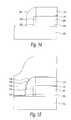
- FIG. 1shows a cross sectional view of an Si/SiGe/Si structure.
- FIG. 2shows a perspective view of a fin portion of a silicon layer and a portion of an SiGe layer defined above a semiconductor substrate, and a support structure attached to the fin portion and the semiconductor substrate.
- FIG. 3shows a perspective view of a fin portion of a silicon layer suspended above a semiconductor substrate with a void therebetween.
- FIGS. 4 to 13show cross sectional views of portions of a semiconductor structure at various stages of an embodiment of a method of the present invention.
- FIGS. 14 to 22show cross sectional views of portions of a semiconductor structure at various stages of another embodiment of a method of the present invention.
- FIGS. 23 to 28 and 30show cross sectional views and FIGS. 29 and 31 show top views, of portions of a semiconductor structure at various stages of yet another embodiment of a method of the present invention.
- the present inventionprovides a method of producing a fin structure on a semiconductor substrate using a thin SiGe layer to produce a void between a silicon substrate and a silicon fin portion.
- a portion of silicon layer in the shape of the desired fin structureis suspended above the semiconductor substrate by a supporting structure, while a portion of the SiGe layer is removed to form a void that either remains as a void in the completed FinFET or is filled with an insulating material.
- the use of conventional wafers, such as a silicon wafer, in the method of the present inventiondecreases the cost of producing FinFET's over the use of an SOI substrate.
- the method of the present inventionalso allows for the production of fin widths that are smaller than what is possible using traditional photolithography. Using photolithography alone, widths of fin structures are limited by the resolution of the photolithography, typically 30 nanometers (nm). However, the method of the present invention allows for fin widths at least as narrow as about 10 nm, without the use of the more expensive SOI techniques.
- a conventional semiconductor substrategenerally represented by reference numeral 102 , such as a conventional silicon wafer, is provided.
- a thin silicon germanium (SiGe) layer 104On the semiconductor substrate 102 is a thin silicon germanium (SiGe) layer 104 .
- the SiGe layer 104may be an epitaxial grown layer.
- the SiGe layer 104is a single crystal layer, which is strained to provide a matching lattice constant to the semiconductor substrate 102 .
- On the SiGe layer 104opposite semiconductor substrate 102 , is provided a silicon layer 106 .
- the silicon layer 106can also be a single crystal layer.
- the SiGe layer 104is produced by germanium implantation in a conventional silicon semiconductor wafer. High temperature annealing is used to remove implantation damage and to form a layer of buried SiGe in the silicon wafer to provide the Si/SiGe/Si structure 100 having a semiconductor substrate 102 , an SiGe layer 104 , and a silicon layer 106 .
- the layer thickness for semiconductor substrate 102can be any thickness that is mechanically strong enough to support a chip.
- the layer thickness for SiGe layer 104can be from about 10 nm to about 30 nm. Preferably, the layer thickness for SiGe layer 104 can be from about 20 nm to about 25 nm. More preferably, the layer thickness for SiGe layer 104 can be from about 20 nm to about 25 nm.
- the layer thickness for silicon layer 106can be from about 30 nm to about 100 nm. Preferably, the layer thickness for silicon layer 106 can be from about 40 nm to about 80 nm. More preferably, the layer thickness for silicon layer 106 can be from about 50 nm to about 70 nm.
- fin portion 124 of silicon layer 106has thereunder a second portion 126 of SiGe layer 104 .
- a support structure 105is connected to fin portion 124 and semiconductor substrate 102 . Any support structure that suspends the fin portion 124 above the semiconductor substrate 102 while the second portion 126 of SiGe layer 104 is removed, is suitable. Support structure 105 can be removed prior to completion of the fin structure or can be an integral part of a completed FinFET.
- first void 130may be filled with an insulating material, such as a nitride, an oxide, a low-k dielectric, or any combinations thereof.
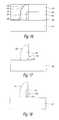
- FIGS. 4 to 13show cross sectional views of portions of a semiconductor structure at various stages of an embodiment of a method of the present invention.
- An Si/SiGe/Si structure 100as in FIG. 1 , is provided.
- silicon layer 106opposite SiGe layer 104 , has a first blocking layer 110 deposited thereon.
- the poly-silicon layer 112may have a layer thickness from about 70 nm to about 120 nm. Examples of suitable materials for the poly-silicon layer 112 include, but are not limited to, poly-silicon, poly-silicon/germanium, nitride, or any combinations thereof.
- the use of a second blocking layer on the poly-silicon layer 112can protect the portions of the poly-silicon layer during subsequent etching.
- Poly-silicon/germaniumhas a different etch rate and does not require the use of an additional blocking layer on the poly-silicon layer 112 .
- the layer thickness for first blocking layer 110can be from about 5 nm to about 10 nm.
- the layer thickness for first blocking layer 110can be from about 8 nm to about 10 nm. More preferably, the layer thickness for first blocking layer 110 can be from about 9 nm to about 10 nm.
- poly-silicon layer 112 and the first blocking layer 110are patterned to reveal a first portion 114 of silicon layer 106 and a first portion 116 of the SiGe layer 104 . This patterning also produces a sidewall 118 of the poly-silicon layer 112 and a sidewall 120 of the first blocking layer 110 .
- the sidewalls 118 and 120 of the poly-silicon layer 112 and first blocking layer 110have deposited or formed thereon a first spacer 122 .
- the first spacer 122may have any suitable material to act as a mask to cover and define thereunder a second portion 124 of the silicon layer 106 and a second portion 126 of the SiGe layer 104 .
- the second portion 124 of the silicon layer 106will form a part of the fin structure.
- An example of a material for the first blocking layerincludes, but is not limited to, a nitride.
- the first portion 114 of silicon layer 106is removed revealing a first sidewall 128 of second portion 124 of silicon layer 106 and leaving the second portion 124 of silicon layer 106 .
- suitable ways to remove the first portion 114 of silicon layer 106include, but are not limited to, etching, reactive ion etch (RIE), or any combinations thereof.
- the first portion 116 of SiGe layer 104is removed revealing a first sidewall 129 of SiGe layer 104 .
- suitable ways to remove the first portion 116 of SiGe layer 104include, but are not limited to, etching, reactive ion etch, or any combinations thereof. Removal of the first portion 116 of SiGe layer 104 is done selective to the material of semiconductor substrate 102 , such that the material of the semiconductor substrate 102 is not removed during the step of removing the first portion 116 of SiGe layer 104 .
- the second portion 126 of SiGe layer 104is removed revealing a first void 130 , as shown in FIG. 8 , between the semiconductor layer 102 and the second portion 124 of silicon layer 106 .
- suitable ways to remove second portion 126 of SiGe layer 104include, but are not limited to, wet etching, RIE, or any combinations thereof.
- the first void 130has the volume under the second portion 124 of silicon layer 106 .
- additional material of SiGe layer 104may also be removed during this step. The removal is done selective to the material of semiconductor substrate 102 .
- Some of the second portion 126 of SiGe layer 104may have already been removed during the step of removing first portion 116 of SiGe layer 104 .
- the remaining SiGe layer 104 , silicon layer 106 , first blocking layer 110 , and poly-silicon layer 112act to support second portion 124 of silicon layer 106 over first void 130 .
- a first insulating material 134is deposited in the first void 130 , on the sidewall 128 of second portion 124 of silicon layer 106 , and on the first spacer 122 .
- suitable materials for use in or for first insulating material 134include, but are not limited to, an oxide, a nitride, oxynitride, low-k material, or any combinations thereof.
- a third blocking layer 135is deposited on first insulating material 134 in order to block subsequent removal of first insulating material 134 during the removal of poly-silicon layer 112 and first blocking layer 110 .
- suitable materials for use in or for third blocking layer 135include, but are not limited to, poly-silicon, poly-silicon germanium, or any combinations thereof.
- the thickness of the third blocking layer 135is preferably greater than the sum of the thicknesses of the SiGe layer 104 , silicon layer 106 , first blocking layer 110 , and poly-silicon layer 112 .
- FIG. 11shows the result of chemical mechanical polishing (CMP) which stops on the top of first spacer 122 . This removes first insulating material 134 that is covering the poly-silicon layer 112 , and any optional second blocking layer.
- CMPchemical mechanical polishing
- poly-silicon layer 112 , part of third blocking layer 135 , and first blocking layer 110 that remain, as in FIG. 11are removed.
- suitable ways to remove poly-silicon layer 112 and first blocking layer 110include RIE or any conventional dry etch methods.
- the portion of silicon layer 106 in FIG. 11 that is not part of second portion 124is removed, revealing a second sidewall 136 of second portion 124 of silicon layer 106 , as seen in FIG. 12 .
- An example of a suitable way to remove portions of silicon layer 106 that are not part of second portion 124includes, but is not limited to, RIE.
- the remaining SiGe layer 104is removed. Preferably, this removal is done selective to the material of semiconductor layer 102 .
- suitable ways to remove remaining SiGe layer 104include, but are not limited to, wet etching, RIE, or any combinations thereof.
- any excess first insulating material 134 covering semiconductor substrate 102can also be removed. Insulating material 134 will be used to support second portion 124 of silicon layer 106 and first spacer 122 upon the removal of the remaining poly-silicon layer 112 , remaining first blocking layer 110 , remaining silicon layer 106 that is not a part of second portion 124 , and remaining SiGe layer 104 . Enough first insulating material 134 must remain to perform this function.
- first insulating material 134 that is not under second portion 124 of silicon layer 106(that part that is in the first void) is removed.
- suitable ways to remove such first insulating material 134include, but are not limited to, wet etching, dry etch, or any combinations thereof.
- the first insulating material 134is asymmetrical as shown in FIG. 13 .
- first insulating material 134is suitable for use as a gate insulating material, such as a gate oxide, it may be desirable to leave first insulating material 134 that is not under second portion 124 of silicon layer 106 .
- a second insulating material(not shown) may be deposited using a suitable technique, such as high density plasma deposition (HDP) on side wall 136 of second portion 124 of silicon layer 106 and other surfaces, such as semiconductor substrate 102 and first spacer 122 , prior to etching and formation of FinFET using conventional processes.
- HDPhigh density plasma deposition
- a fin structureis produced using a method similar to that described above.
- FIGS. 1 , 4 to 7 and 14 to 22cross sectional views of semiconductor structures at various stages of a method of producing a fin structure are shown. The method involves the same steps as described in the embodiment above up to and including the removal of first portion 116 of SiGe layer 104 as in FIG. 7 . Thereafter, on sidewall 118 of poly-silicon layer 112 , sidewall 120 of first blocking layer 110 , sidewall 128 of second portion 124 of silicon layer 106 , and sidewall 129 of second portion 126 of SiGe layer 104 , a second spacer 140 is formed as shown in FIG. 14 .
- the second spacer 140can be of the same or different material as first spacer 122 of FIG. 6 .
- the second spacer 140can be formed after the removal of all or part of the first spacer or can be formed on top of the existing first spacer.
- the second spacer 140can include any suitable material for supporting second portion 124 of silicon layer 106 upon the removal of poly-silicon layer 112 , first blocking layer 110 , the portion of silicon layer 106 not part of second portion 124 , and SiGe layer 104 , as will be described in detail below.
- Examples of materials for use in or for second spacer 140include, but are not limited to, a nitride, oxynitride, or any combinations thereof.
- first insulating material 134is deposited on semiconductor substrate 102 , second spacer 140 , and poly-silicon layer 112 .
- Third blocking layer 135is deposited on first insulating material 134 .
- FIG. 16shows the result of chemical mechanical polishing (CMP) of third blocking layer 135 and first insulating material 134 stopping on the top of second spacer 140 .
- CMPchemical mechanical polishing
- any optional second blocking layer material (not shown) remaining on poly-silicon layer 112is removed.
- Remaining poly-silicon layer 112 , third blocking layer 135 , and first blocking layer 110are removed. This removal may be by any suitable way. Examples of ways to remove poly-silicon layer 112 and first blocking layer 110 include, but are not limited to, RIE, dry etch, or any combinations thereof.
- the portions of silicon layer 106 that are not part of second portion 124are removed, revealing a second sidewall 136 of second portion 124 of silicon layer 106 , as in FIG. 17 . This removal may be by any suitable way. Examples of ways to remove portions of silicon layer 106 that are not part of second portion 124 include, but are not limited to, RIE, dry etch, or any combinations thereof.
- the first insulating material 134is removed from first spacer 140 and from semiconductor substrate 102 .
- the SiGe layer 104 that remains, as in FIG. 16is removed. This removal may be done by any suitable way. Preferably, this removal is done selective to the material of semiconductor layer 102 . Examples of ways to remove remaining SiGe layer 104 include, but are not limited to, wet etching, RIE, or any combinations thereof.
- this removal of the remaining SiGe layer 104may be done by wet etching, selective to the material of semiconductor substrate 102 , to remove the SiGe layer 104 including the second portion 126 of SiGe layer 104 to produce a first void 130 beneath second portion 124 of silicon layer 106 and above semiconductor substrate 102 , as in FIG. 17 .
- Second spacer 140acts as a supporting structure to suspend second portion 124 of silicon layer 106 over semiconductor substrate 102 with first void 130 therebetween.
- the removal of the remaining SiGe layer 104may also be done in a step-wise fashion, thereby first removing SiGe layer 104 that is not a part of second portion 126 of SiGe layer 104 first. This removal may be done by etching that part of the SiGe layer 104 selective to the material of the semiconductor layer 102 leaving second portion 126 of SiGe layer 104 in place, as in FIG. 18 . Next, enough heat to induce oxidation of the second portion 126 of SiGe layer 104 is applied.
- An example of an appropriate level of heat to induce oxidationincludes, but is not limited to, about 1,000° Celsius (C) to about 1,200° C.
- FIG. 19shows the formation of oxidation material 150 .
- the oxidation material 150is then removed, as in FIG. 20 , to reveal first void 130 .
- Second portion 124 of silicon layer 106is suspended above the semiconductor substrate 102 by the support mechanism of the second spacer 140 .
- Second spacer 140acts as a supporting structure to suspend second portion 124 of silicon layer 106 over semiconductor substrate 102 with first void 130 therebetween.
- first insulating material 152is deposited.
- suitable ways for depositing first insulating material 152include, but are not limited to, direct deposition, HDP, or any combinations thereof.
- materials for use in or for the first insulating materialinclude, but are not limited to, an oxide, a nitride, low-k material, or any combinations thereof.
- second spacer 140is removed.
- This removal of second spacer 140may be done by any suitable way.
- ways to remove second spacer 140include, but are not limited to, wet etching, dry etch, or any combinations thereof.
- the first insulating material 152 that is not in first void 130 , as in FIG. 21is removed. This removal may be done by any suitable way. Examples of ways to remove such first insulating material 134 include, but are not limited to, RIE, dry etch, or any combinations thereof.
- This produces a fin structure 154as in FIG. 22 , on semiconductor substrate 102 . Thereafter, conventional processes for forming a FinFET can be followed.
- an Si/SiGe/Si structure 100is provided.
- a first blocking layer 160on silicon layer 106 is deposited a first blocking layer 160 .
- materials for use in or for the first blocking layer 160include, but are not limited to, a nitride, oxide, or any combinations thereof.
- the layer thickness for first blocking layer 160is from about 5 nm to about 20 nm.
- the layer thickness for first blocking layer 160is from about 8 nm to about 15 nm. More preferably, the layer thickness for first blocking layer 160 is from about 8 nm to about 10 nm.
- first photoresist material 162On first blocking layer 160 , opposite silicon layer 106 , is deposited a first photoresist material 162 .
- the layer thickness for first photoresist material 162is from about 100 nm to about 400 nm. Preferably, the layer thickness for first photoresist material 162 is from about 150 nm to about 300 nm. More preferably, the layer thickness for first photoresist material 162 can be from about 200 nm to about 250 nm.
- the first photoresist material 162is patterned to form the pattern of the desired fin structure with second portion 124 of silicon layer 106 and second portion 126 of SiGe layer 104 defined under the pattern.
- the first blocking layer 160 not beneath the first photoresist material 162is removed.
- the first blocking layer 160may be removed by any suitable way. Examples of ways to remove first blocking layer 160 include, but are not limited to, RIE, dry etch, or any combinations thereof.
- the silicon layer 106 not part of second portion 124 of silicon layer 106 and SiGe layer 104 not part of second portion 126 of SiGe layer 104are removed by any suitable way to leave second portion 124 of silicon layer 106 having a first sidewall 164 and a second sidewall 168 .
- the second portion 124 of silicon layer 106is the fin portion that will be suspended above semiconductor substrate 102 in the steps below.
- Examples of ways for removing silicon layer 106 and SiGe layer 104include, but are not limited to, RIE, dry etch, or any combinations thereof.
- the removal of silicon layer 106is selective to the material of SiGe layer 104 and the removal of SiGe layer 104 is selective to the material of semiconductor layer 102 .
- first photoresist material 162is removed.
- suitable ways to remove first photoresist material 162include, but are not limited to, etching.
- first insulating material 170is deposited thereon.
- first insulating material 170is deposited by high density plasma (HDP) deposition. This method results in thicker oxide on the top of semiconductor substrate 102 and first blocking layer 160 , but thinner oxide on first and second sidewalls of second portion 124 of silicon layer 106 .
- materials suitable for use in or for first insulating material 170include, but are not limited to, an oxide, a nitride, or any combinations thereof.
- any first insulating material 170 on first and second sidewalls of second portion 124 of silicon layer 106are removed to expose the sidewall for formation of gate insulating material 172 .
- the layer thickness for first insulating material 170is from about 10 nm to about 50 nm. Preferably, the layer thickness for first insulating material 170 is from about 10 nm to about 30 nm. More preferably, the layer thickness for first insulating material 170 is from about 25 nm to about 30 nm.
- gate insulating material 172such as a gate-oxide, is formed on the first and second sidewalls of silicon fin 164 .
- suitable ways to form gate insulating material 172include, but are not limited to, oxidation, deposition of high-k dielectric, or any combinations thereof.
- materials suitable for use in or for gate insulating material 172include, but are not limited to, an oxide, high-k material, or any combinations thereof.
- the layer thickness for gate insulating material 172is from about 0.7 nm to about 3 nm.
- the layer thickness for gate insulating material 172is from about 0.8 nm to about 2 nm. More preferably, the layer thickness for gate insulating material 172 is from about 0.8 nm to about 0.9 nm.
- a gate layer 174is deposited.
- suitable ways to deposit gate layer 174include, but are not limited to, chemical vapor deposition.
- materials suitable for use in or for gate layer 174include, but are not limited to, poly-silicon, poly-silicon/germanium, or any combinations thereof.
- the layer thickness for gate layer 174is from about 50 nm to about 200 nm.
- the layer thickness for gate layer 174is from about 70 nm to about 150 nm. More preferably, the layer thickness for gate layer 174 is from about 100 nm to about 120 nm.
- gate layer 174has deposited thereon a second photoresist material 176 .
- the second photoresist material 176is patterned to define a gate region 186 thereunder for etching the gate material 174 and first insulating material 170 that is not part of the gate region 186 under the second photoresist material.
- the gate material 174 not covered by patterned second photoresist material 176is removed. Examples of suitable ways to remove gate material 174 include, but are not limited to, RIE, dry etch, or any combinations thereof.
- the first insulating material 170 not covered by patterned second photoresist material 176is removed.
- suitable ways to remove first insulating material 170include, but are not limited to, RIE, dry etch, or any combinations thereof.
- the removal of first insulating material 170is done selective to the material of semiconductor substrate 102 .
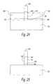
- the second portion 126 of SiGe layer 104is removed to produce a first void 178 having an upper boundary 180 defined by the lower surface of the second portion 124 of silicon layer 106 and a lower boundary 182 defined by a portion of the upper surface of the semiconductor substrate 102 that is underneath the second portion 124 of the silicon layer 106 .
- the removal of the second portion 126 of SiGe layer 104is preferably selective to the material of the semiconductor substrate 102 and the fin 124 . Examples of suitable ways for removing second portion 126 of SiGe layer 104 include, but are not limited to, wet etching, dry etch, or any combinations thereof.
- FIG. 29shows a top view of a semiconductor structure at this stage of the method.
- the top surface 182 of semiconductor substrate 102is sectioned by the fin structure 184 and gate region 186 .
- the top surface of the fin structure 184has material of the first blocking layer.
- the top surface of the gate region 186has material of the second photoresist. Referring to FIGS. 28 and 29 , beneath the intersection of the fin structure 184 and gate region 186 , and between the suspended second portion 124 of silicon layer 106 and semiconductor substrate 102 , is the first void 178 .
- first void 178as a void or filling first void 178 with an insulating material, such as an oxide, a nitride, or low-k material. Leaving first void 178 as a void provides a low capacitance. If the void is filled by nitride, the completed FinFET has high heat conduction to the substrate due to high thermal conductivity of nitride.
- an insulating materialsuch as an oxide, a nitride, or low-k material.
- second photoresist material 176can be removed before or after the creation of first void 178 .
- suitable ways to remove second photoresist material 176include, but are not limited to, etching.
- first void 178when leaving first void 178 , as shown in FIG. 28 , as a void, it is preferred that the upper boundary 180 , and optionally lower boundary 182 , of first void 178 be re-oxidized to protect the lower surface of the second portion 124 of silicon layer 106 .
- FIG. 30shows a cross sectional view and FIG. 31 shows a top view of a semiconductor substrate at this stage of a method of the present invention.
- FIG. 30shows re-oxidized regions 190 and 192 .
- top surface 182 of semiconductor substrate 102has deposited thereon a third insulating material.
- An examples of a suitable way to deposit third insulating material 188includes HDP deposition in order to cover the surface of the substrate.
- suitable materials for use in or for third insulating material 188include, but are not limited to, an oxide, nitride, or any combinations thereof.
- a preferred material for use in or for third insulating material 188is an oxide.
- the layer thickness for third insulating material 188can be from about 20 nm to about 50 nm.
- the top surface of the fin structure 184may also have deposited thereon third insulating material 188 .
- a top surface of gate region 186may also have deposited thereon third insulating material 188 . Referring to FIGS. 30 and 31 , beneath the intersection of the fin structure 184 and gate region 186 , and between the suspended second portion 124 of silicon layer 106 and semiconductor substrate 102 , is the first void 178 .
Landscapes
- Thin Film Transistor (AREA)
Abstract
Description
Claims (14)
Priority Applications (1)
| Application Number | Priority Date | Filing Date | Title |
|---|---|---|---|
| US11/835,182US7800152B2 (en) | 2004-04-15 | 2007-08-07 | Methods for manufacturing a finfet using a conventional wafer and apparatus manufactured therefrom |
Applications Claiming Priority (2)
| Application Number | Priority Date | Filing Date | Title |
|---|---|---|---|
| US10/709,129US7262084B2 (en) | 2004-04-15 | 2004-04-15 | Methods for manufacturing a finFET using a conventional wafer and apparatus manufactured therefrom |
| US11/835,182US7800152B2 (en) | 2004-04-15 | 2007-08-07 | Methods for manufacturing a finfet using a conventional wafer and apparatus manufactured therefrom |
Related Parent Applications (1)
| Application Number | Title | Priority Date | Filing Date |
|---|---|---|---|
| US10/709,129DivisionUS7262084B2 (en) | 2004-04-15 | 2004-04-15 | Methods for manufacturing a finFET using a conventional wafer and apparatus manufactured therefrom |
Publications (2)
| Publication Number | Publication Date |
|---|---|
| US20080048233A1 US20080048233A1 (en) | 2008-02-28 |
| US7800152B2true US7800152B2 (en) | 2010-09-21 |
Family
ID=35096817
Family Applications (2)
| Application Number | Title | Priority Date | Filing Date |
|---|---|---|---|
| US10/709,129Expired - Fee RelatedUS7262084B2 (en) | 2004-04-15 | 2004-04-15 | Methods for manufacturing a finFET using a conventional wafer and apparatus manufactured therefrom |
| US11/835,182Expired - Fee RelatedUS7800152B2 (en) | 2004-04-15 | 2007-08-07 | Methods for manufacturing a finfet using a conventional wafer and apparatus manufactured therefrom |
Family Applications Before (1)
| Application Number | Title | Priority Date | Filing Date |
|---|---|---|---|
| US10/709,129Expired - Fee RelatedUS7262084B2 (en) | 2004-04-15 | 2004-04-15 | Methods for manufacturing a finFET using a conventional wafer and apparatus manufactured therefrom |
Country Status (1)
| Country | Link |
|---|---|
| US (2) | US7262084B2 (en) |
Cited By (10)
| Publication number | Priority date | Publication date | Assignee | Title |
|---|---|---|---|---|
| US20110129978A1 (en)* | 2009-12-01 | 2011-06-02 | Kangguo Cheng | Method and structure for forming finfets with multiple doping regions on a same chip |
| US20140264594A1 (en)* | 2013-03-14 | 2014-09-18 | International Business Machines Corporation | FORMATION OF BULK SiGe FIN WITH DIELECTRIC ISOLATION BY ANODIZATION |
| US8946027B2 (en) | 2012-02-07 | 2015-02-03 | International Business Machines Corporation | Replacement-gate FinFET structure and process |
| US9000522B2 (en) | 2013-01-09 | 2015-04-07 | International Business Machines Corporation | FinFET with dielectric isolation by silicon-on-nothing and method of fabrication |
| US9385218B1 (en) | 2015-04-23 | 2016-07-05 | International Business Machines Corporation | Method and structure for forming dielectric isolated FinFET with improved source/drain epitaxy |
| US9679780B1 (en) | 2016-09-28 | 2017-06-13 | International Business Machines Corporation | Polysilicon residue removal in nanosheet MOSFETs |
| US9929155B2 (en)* | 2015-04-02 | 2018-03-27 | Samsung Electronics Co., Ltd. | Semiconductor device having symmetric and asymmetric active fins |
| CN108807544A (en)* | 2013-06-26 | 2018-11-13 | 美商新思科技有限公司 | The FinFET controlled with hetero-junctions and improved raceway groove |
| US10896816B2 (en) | 2017-09-26 | 2021-01-19 | International Business Machines Corporation | Silicon residue removal in nanosheet transistors |
| US20220254689A1 (en)* | 2021-02-09 | 2022-08-11 | Tokyo Electron Limited | Method of making vertical semiconductor nanosheets with diffusion breaks |
Families Citing this family (22)
| Publication number | Priority date | Publication date | Assignee | Title |
|---|---|---|---|---|
| US7049662B2 (en)* | 2003-11-26 | 2006-05-23 | International Business Machines Corporation | Structure and method to fabricate FinFET devices |
| KR100645065B1 (en)* | 2005-06-23 | 2006-11-10 | 삼성전자주식회사 | Fin Field Effect Transistor, Nonvolatile Memory Device Having Same and Forming Method Thereof |
| US7352034B2 (en)* | 2005-08-25 | 2008-04-01 | International Business Machines Corporation | Semiconductor structures integrating damascene-body FinFET's and planar devices on a common substrate and methods for forming such semiconductor structures |
| US8227316B2 (en)* | 2006-06-29 | 2012-07-24 | International Business Machines Corporation | Method for manufacturing double gate finFET with asymmetric halo |
| US7811890B2 (en)* | 2006-10-11 | 2010-10-12 | Macronix International Co., Ltd. | Vertical channel transistor structure and manufacturing method thereof |
| US8772858B2 (en) | 2006-10-11 | 2014-07-08 | Macronix International Co., Ltd. | Vertical channel memory and manufacturing method thereof and operating method using the same |
| US7851848B2 (en)* | 2006-11-01 | 2010-12-14 | Macronix International Co., Ltd. | Cylindrical channel charge trapping devices with effectively high coupling ratios |
| US7772048B2 (en)* | 2007-02-23 | 2010-08-10 | Freescale Semiconductor, Inc. | Forming semiconductor fins using a sacrificial fin |
| KR100861211B1 (en)* | 2007-04-12 | 2008-09-30 | 주식회사 하이닉스반도체 | Semiconductor device and manufacturing method thereof |
| US7838923B2 (en)* | 2007-08-09 | 2010-11-23 | Macronix International Co., Ltd. | Lateral pocket implant charge trapping devices |
| US7736965B2 (en)* | 2007-12-06 | 2010-06-15 | International Business Machines Corporation | Method of making a FinFET device structure having dual metal and high-k gates |
| US8860124B2 (en)* | 2009-01-15 | 2014-10-14 | Macronix International Co., Ltd. | Depletion-mode charge-trapping flash device |
| US8633573B2 (en)* | 2009-02-16 | 2014-01-21 | The Board Of Trustees Of The Leland Stanford Junior University | Strained semiconductor materials, devices and methods therefore |
| US8912602B2 (en)* | 2009-04-14 | 2014-12-16 | Taiwan Semiconductor Manufacturing Company, Ltd. | FinFETs and methods for forming the same |
| CN103855027B (en) | 2012-12-06 | 2017-01-25 | 中国科学院微电子研究所 | Finfet and manufacturing method thereof |
| US9029913B2 (en)* | 2013-03-11 | 2015-05-12 | International Business Machines Corporation | Silicon-germanium fins and silicon fins on a bulk substrate |
| CN103258724B (en)* | 2013-05-09 | 2016-09-28 | 清华大学 | There is three-dimensional semiconductor device of large ratio of height to width FIN structure and forming method thereof |
| US9349863B2 (en) | 2013-08-07 | 2016-05-24 | Globalfoundries Inc. | Anchored stress-generating active semiconductor regions for semiconductor-on-insulator finfet |
| CN103904122B (en)* | 2014-04-04 | 2017-04-26 | 唐棕 | Fin-type semiconductor structure and forming method thereof |
| US9269814B2 (en)* | 2014-05-14 | 2016-02-23 | Taiwan Semiconductor Manufacturing Co., Ltd. | Sacrificial layer fin isolation for fin height and leakage control of bulk finFETs |
| US9484461B2 (en) | 2014-09-29 | 2016-11-01 | Taiwan Semiconductor Manufacturing Company, Ltd. | Integrated circuit structure with substrate isolation and un-doped channel |
| US10516021B2 (en)* | 2015-12-24 | 2019-12-24 | Intel Corporation | Reduced leakage transistors with germanium-rich channel regions |
Citations (21)
| Publication number | Priority date | Publication date | Assignee | Title |
|---|---|---|---|---|
| US6190996B1 (en)* | 1997-11-12 | 2001-02-20 | Micron Technology, Inc. | Method of making an insulator for electrical structures |
| US6300182B1 (en) | 2000-12-11 | 2001-10-09 | Advanced Micro Devices, Inc. | Field effect transistor having dual gates with asymmetrical doping for reduced threshold voltage |
| US6391695B1 (en) | 2000-08-07 | 2002-05-21 | Advanced Micro Devices, Inc. | Double-gate transistor formed in a thermal process |
| US6403434B1 (en) | 2001-02-09 | 2002-06-11 | Advanced Micro Devices, Inc. | Process for manufacturing MOS transistors having elevated source and drain regions and a high-k gate dielectric |
| US6413802B1 (en) | 2000-10-23 | 2002-07-02 | The Regents Of The University Of California | Finfet transistor structures having a double gate channel extending vertically from a substrate and methods of manufacture |
| US6451656B1 (en) | 2001-02-28 | 2002-09-17 | Advanced Micro Devices, Inc. | CMOS inverter configured from double gate MOSFET and method of fabricating same |
| US6475869B1 (en) | 2001-02-26 | 2002-11-05 | Advanced Micro Devices, Inc. | Method of forming a double gate transistor having an epitaxial silicon/germanium channel region |
| US6475890B1 (en) | 2001-02-12 | 2002-11-05 | Advanced Micro Devices, Inc. | Fabrication of a field effect transistor with an upside down T-shaped semiconductor pillar in SOI technology |
| US6492212B1 (en) | 2001-10-05 | 2002-12-10 | International Business Machines Corporation | Variable threshold voltage double gated transistors and method of fabrication |
| US6521502B1 (en) | 2000-08-07 | 2003-02-18 | Advanced Micro Devices, Inc. | Solid phase epitaxy activation process for source/drain junction extensions and halo regions |
| US6525403B2 (en) | 2000-09-28 | 2003-02-25 | Kabushiki Kaisha Toshiba | Semiconductor device having MIS field effect transistors or three-dimensional structure |
| US6562665B1 (en) | 2000-10-16 | 2003-05-13 | Advanced Micro Devices, Inc. | Fabrication of a field effect transistor with a recess in a semiconductor pillar in SOI technology |
| US20030102497A1 (en) | 2001-12-04 | 2003-06-05 | International Business Machines Corporation | Multiple-plane finFET CMOS |
| US6580137B2 (en) | 2000-08-29 | 2003-06-17 | Boise State University | Damascene double gated transistors and related manufacturing methods |
| US6583469B1 (en) | 2002-01-28 | 2003-06-24 | International Business Machines Corporation | Self-aligned dog-bone structure for FinFET applications and methods to fabricate the same |
| US6605514B1 (en) | 2002-07-31 | 2003-08-12 | Advanced Micro Devices, Inc. | Planar finFET patterning using amorphous carbon |
| US6611029B1 (en) | 2002-11-08 | 2003-08-26 | Advanced Micro Devices, Inc. | Double gate semiconductor device having separate gates |
| US6610576B2 (en) | 2001-12-13 | 2003-08-26 | International Business Machines Corporation | Method for forming asymmetric dual gate transistor |
| US6642090B1 (en) | 2002-06-03 | 2003-11-04 | International Business Machines Corporation | Fin FET devices from bulk semiconductor and method for forming |
| US6727186B1 (en)* | 1999-06-28 | 2004-04-27 | FRANCE TéLéCOM | Method for lateral etching with holes for making semiconductor devices |
| US6844238B2 (en)* | 2003-03-26 | 2005-01-18 | Taiwan Semiconductor Manufacturing Co., Ltd | Multiple-gate transistors with improved gate control |
- 2004
- 2004-04-15USUS10/709,129patent/US7262084B2/ennot_activeExpired - Fee Related
- 2007
- 2007-08-07USUS11/835,182patent/US7800152B2/ennot_activeExpired - Fee Related
Patent Citations (21)
| Publication number | Priority date | Publication date | Assignee | Title |
|---|---|---|---|---|
| US6190996B1 (en)* | 1997-11-12 | 2001-02-20 | Micron Technology, Inc. | Method of making an insulator for electrical structures |
| US6727186B1 (en)* | 1999-06-28 | 2004-04-27 | FRANCE TéLéCOM | Method for lateral etching with holes for making semiconductor devices |
| US6391695B1 (en) | 2000-08-07 | 2002-05-21 | Advanced Micro Devices, Inc. | Double-gate transistor formed in a thermal process |
| US6521502B1 (en) | 2000-08-07 | 2003-02-18 | Advanced Micro Devices, Inc. | Solid phase epitaxy activation process for source/drain junction extensions and halo regions |
| US6580137B2 (en) | 2000-08-29 | 2003-06-17 | Boise State University | Damascene double gated transistors and related manufacturing methods |
| US6525403B2 (en) | 2000-09-28 | 2003-02-25 | Kabushiki Kaisha Toshiba | Semiconductor device having MIS field effect transistors or three-dimensional structure |
| US6562665B1 (en) | 2000-10-16 | 2003-05-13 | Advanced Micro Devices, Inc. | Fabrication of a field effect transistor with a recess in a semiconductor pillar in SOI technology |
| US6413802B1 (en) | 2000-10-23 | 2002-07-02 | The Regents Of The University Of California | Finfet transistor structures having a double gate channel extending vertically from a substrate and methods of manufacture |
| US6300182B1 (en) | 2000-12-11 | 2001-10-09 | Advanced Micro Devices, Inc. | Field effect transistor having dual gates with asymmetrical doping for reduced threshold voltage |
| US6403434B1 (en) | 2001-02-09 | 2002-06-11 | Advanced Micro Devices, Inc. | Process for manufacturing MOS transistors having elevated source and drain regions and a high-k gate dielectric |
| US6475890B1 (en) | 2001-02-12 | 2002-11-05 | Advanced Micro Devices, Inc. | Fabrication of a field effect transistor with an upside down T-shaped semiconductor pillar in SOI technology |
| US6475869B1 (en) | 2001-02-26 | 2002-11-05 | Advanced Micro Devices, Inc. | Method of forming a double gate transistor having an epitaxial silicon/germanium channel region |
| US6451656B1 (en) | 2001-02-28 | 2002-09-17 | Advanced Micro Devices, Inc. | CMOS inverter configured from double gate MOSFET and method of fabricating same |
| US6492212B1 (en) | 2001-10-05 | 2002-12-10 | International Business Machines Corporation | Variable threshold voltage double gated transistors and method of fabrication |
| US20030102497A1 (en) | 2001-12-04 | 2003-06-05 | International Business Machines Corporation | Multiple-plane finFET CMOS |
| US6610576B2 (en) | 2001-12-13 | 2003-08-26 | International Business Machines Corporation | Method for forming asymmetric dual gate transistor |
| US6583469B1 (en) | 2002-01-28 | 2003-06-24 | International Business Machines Corporation | Self-aligned dog-bone structure for FinFET applications and methods to fabricate the same |
| US6642090B1 (en) | 2002-06-03 | 2003-11-04 | International Business Machines Corporation | Fin FET devices from bulk semiconductor and method for forming |
| US6605514B1 (en) | 2002-07-31 | 2003-08-12 | Advanced Micro Devices, Inc. | Planar finFET patterning using amorphous carbon |
| US6611029B1 (en) | 2002-11-08 | 2003-08-26 | Advanced Micro Devices, Inc. | Double gate semiconductor device having separate gates |
| US6844238B2 (en)* | 2003-03-26 | 2005-01-18 | Taiwan Semiconductor Manufacturing Co., Ltd | Multiple-gate transistors with improved gate control |
Cited By (19)
| Publication number | Priority date | Publication date | Assignee | Title |
|---|---|---|---|---|
| US8021949B2 (en)* | 2009-12-01 | 2011-09-20 | International Business Machines Corporation | Method and structure for forming finFETs with multiple doping regions on a same chip |
| US20110129978A1 (en)* | 2009-12-01 | 2011-06-02 | Kangguo Cheng | Method and structure for forming finfets with multiple doping regions on a same chip |
| US8946027B2 (en) | 2012-02-07 | 2015-02-03 | International Business Machines Corporation | Replacement-gate FinFET structure and process |
| US9219068B2 (en) | 2013-01-09 | 2015-12-22 | Globalfoundries Inc | FinFET with dielectric isolation by silicon-on-nothing and method of fabrication |
| US9478549B2 (en) | 2013-01-09 | 2016-10-25 | Globalfoundries Inc. | FinFET with dielectric isolation by silicon-on-nothing and method of fabrication |
| US9000522B2 (en) | 2013-01-09 | 2015-04-07 | International Business Machines Corporation | FinFET with dielectric isolation by silicon-on-nothing and method of fabrication |
| US8975125B2 (en)* | 2013-03-14 | 2015-03-10 | International Business Machines Corporation | Formation of bulk SiGe fin with dielectric isolation by anodization |
| US20140264594A1 (en)* | 2013-03-14 | 2014-09-18 | International Business Machines Corporation | FORMATION OF BULK SiGe FIN WITH DIELECTRIC ISOLATION BY ANODIZATION |
| US9508851B2 (en) | 2013-03-14 | 2016-11-29 | International Business Machines Corporation | Formation of bulk SiGe fin with dielectric isolation by anodization |
| CN108807544A (en)* | 2013-06-26 | 2018-11-13 | 美商新思科技有限公司 | The FinFET controlled with hetero-junctions and improved raceway groove |
| CN108807544B (en)* | 2013-06-26 | 2023-03-07 | 美商新思科技有限公司 | FinFETs with heterojunction and improved channel control |
| US9929155B2 (en)* | 2015-04-02 | 2018-03-27 | Samsung Electronics Co., Ltd. | Semiconductor device having symmetric and asymmetric active fins |
| US9385218B1 (en) | 2015-04-23 | 2016-07-05 | International Business Machines Corporation | Method and structure for forming dielectric isolated FinFET with improved source/drain epitaxy |
| US10002926B2 (en) | 2015-04-23 | 2018-06-19 | International Business Machines Corporation | Method and structure for forming dielectric isolated FinFET with improved source/drain epitaxy |
| US9679780B1 (en) | 2016-09-28 | 2017-06-13 | International Business Machines Corporation | Polysilicon residue removal in nanosheet MOSFETs |
| US9997352B2 (en) | 2016-09-28 | 2018-06-12 | International Business Machines Corporation | Polysilicon residue removal in nanosheet MOSFETs |
| US10896816B2 (en) | 2017-09-26 | 2021-01-19 | International Business Machines Corporation | Silicon residue removal in nanosheet transistors |
| US20220254689A1 (en)* | 2021-02-09 | 2022-08-11 | Tokyo Electron Limited | Method of making vertical semiconductor nanosheets with diffusion breaks |
| US11721592B2 (en)* | 2021-02-09 | 2023-08-08 | Tokyo Electron Limited | Method of making vertical semiconductor nanosheets with diffusion breaks |
Also Published As
| Publication number | Publication date |
|---|---|
| US20050233565A1 (en) | 2005-10-20 |
| US20080048233A1 (en) | 2008-02-28 |
| US7262084B2 (en) | 2007-08-28 |
Similar Documents
| Publication | Publication Date | Title |
|---|---|---|
| US7800152B2 (en) | Methods for manufacturing a finfet using a conventional wafer and apparatus manufactured therefrom | |
| US10622261B2 (en) | FinFET devices with unique shape and the fabrication thereof | |
| KR100444095B1 (en) | Method of fabricating semiconductor side wall fin | |
| CN100524667C (en) | Sectional field effect transistor making method | |
| US8637372B2 (en) | Methods for fabricating a FINFET integrated circuit on a bulk silicon substrate | |
| TWI509736B (en) | Semiconductor structure and method of forming same | |
| JP4453967B2 (en) | Strained channel FinFET with uniform channel thickness and isolation gate | |
| US7268058B2 (en) | Tri-gate transistors and methods to fabricate same | |
| US7709892B2 (en) | Semiconductor device having freestanding semiconductor layer | |
| US20110140229A1 (en) | Techniques for forming shallow trench isolation | |
| US7785944B2 (en) | Method of making double-gated self-aligned finFET having gates of different lengths | |
| JP2007142392A (en) | Method, semiconductor structure (quasi self-aligned source / drain fin FET process) | |
| CN102113110B (en) | Semiconductor devices with extended active regions | |
| CN103579004B (en) | Finfet and manufacturing method thereof | |
| CN104103516A (en) | Shallow groove isolation structure and formation method thereof | |
| US20040157396A1 (en) | Methods for forming double gate electrodes using tunnel and trench | |
| US20070102756A1 (en) | FinFET transistor fabricated in bulk semiconducting material | |
| US9882031B2 (en) | Method of manufacturing a horizontal gate-all-around transistor having a fin | |
| US6897122B1 (en) | Wide neck shallow trench isolation region to prevent strain relaxation at shallow trench isolation region edges | |
| US8354319B2 (en) | Integrated planar and multiple gate FETs | |
| JP3558338B2 (en) | Dual / wrap-around-gate field-effect transistor and method of manufacturing the same | |
| US20140038417A1 (en) | Semiconductor structure and process thereof | |
| US7622368B2 (en) | Forming of a single-crystal semiconductor layer portion separated from a substrate | |
| JP2004281661A (en) | Semiconductor device and method of manufacturing the same | |
| KR20060014549A (en) | Method and fabrication method of 3D field effect transistor with gate formed on silicon channel |
Legal Events
| Date | Code | Title | Description |
|---|---|---|---|
| AS | Assignment | Owner name:INTERNATIONAL BUSINESS MACHINES CORPORATION, NEW Y Free format text:CORRECTIVE ASSIGNMENT TO CORRECT THE MISSING CONTINUITY DATA FOR DIVISIONAL APPLICATION 11/835182 PREVIOUSLY RECORDED ON REEL 014504 FRAME 0096. ASSIGNOR(S) HEREBY CONFIRMS THE DIVISIONAL APPLICATION OF 10/709129 WAS NOT CARRIED OVER;ASSIGNORS:ZHU, HUILONG;DORIS, BRUCE B.;SIGNING DATES FROM 20040407 TO 20040409;REEL/FRAME:028252/0692 | |
| REMI | Maintenance fee reminder mailed | ||
| FPAY | Fee payment | Year of fee payment:4 | |
| SULP | Surcharge for late payment | ||
| AS | Assignment | Owner name:GLOBALFOUNDRIES U.S. 2 LLC, NEW YORK Free format text:ASSIGNMENT OF ASSIGNORS INTEREST;ASSIGNOR:INTERNATIONAL BUSINESS MACHINES CORPORATION;REEL/FRAME:036550/0001 Effective date:20150629 | |
| AS | Assignment | Owner name:GLOBALFOUNDRIES INC., CAYMAN ISLANDS Free format text:ASSIGNMENT OF ASSIGNORS INTEREST;ASSIGNORS:GLOBALFOUNDRIES U.S. 2 LLC;GLOBALFOUNDRIES U.S. INC.;REEL/FRAME:036779/0001 Effective date:20150910 | |
| FEPP | Fee payment procedure | Free format text:MAINTENANCE FEE REMINDER MAILED (ORIGINAL EVENT CODE: REM.) | |
| LAPS | Lapse for failure to pay maintenance fees | Free format text:PATENT EXPIRED FOR FAILURE TO PAY MAINTENANCE FEES (ORIGINAL EVENT CODE: EXP.); ENTITY STATUS OF PATENT OWNER: LARGE ENTITY | |
| STCH | Information on status: patent discontinuation | Free format text:PATENT EXPIRED DUE TO NONPAYMENT OF MAINTENANCE FEES UNDER 37 CFR 1.362 | |
| FP | Lapsed due to failure to pay maintenance fee | Effective date:20180921 | |
| AS | Assignment | Owner name:WILMINGTON TRUST, NATIONAL ASSOCIATION, DELAWARE Free format text:SECURITY AGREEMENT;ASSIGNOR:GLOBALFOUNDRIES INC.;REEL/FRAME:049490/0001 Effective date:20181127 | |
| AS | Assignment | Owner name:GLOBALFOUNDRIES INC., CAYMAN ISLANDS Free format text:RELEASE BY SECURED PARTY;ASSIGNOR:WILMINGTON TRUST, NATIONAL ASSOCIATION;REEL/FRAME:054636/0001 Effective date:20201117 | |
| AS | Assignment | Owner name:GLOBALFOUNDRIES U.S. INC., NEW YORK Free format text:RELEASE BY SECURED PARTY;ASSIGNOR:WILMINGTON TRUST, NATIONAL ASSOCIATION;REEL/FRAME:056987/0001 Effective date:20201117 |