US7800135B2 - Power semiconductor device and method of manufacturing a power semiconductor device - Google Patents
Power semiconductor device and method of manufacturing a power semiconductor deviceDownload PDFInfo
- Publication number
- US7800135B2 US7800135B2US11/996,681US99668105AUS7800135B2US 7800135 B2US7800135 B2US 7800135B2US 99668105 AUS99668105 AUS 99668105AUS 7800135 B2US7800135 B2US 7800135B2
- Authority
- US
- United States
- Prior art keywords
- face
- drain
- base
- region
- junction
- Prior art date
- Legal status (The legal status is an assumption and is not a legal conclusion. Google has not performed a legal analysis and makes no representation as to the accuracy of the status listed.)
- Active, expires
Links
Images


Classifications
- H—ELECTRICITY
- H10—SEMICONDUCTOR DEVICES; ELECTRIC SOLID-STATE DEVICES NOT OTHERWISE PROVIDED FOR
- H10D—INORGANIC ELECTRIC SEMICONDUCTOR DEVICES
- H10D30/00—Field-effect transistors [FET]
- H10D30/60—Insulated-gate field-effect transistors [IGFET]
- H10D30/64—Double-diffused metal-oxide semiconductor [DMOS] FETs
- H10D30/66—Vertical DMOS [VDMOS] FETs
- H—ELECTRICITY
- H10—SEMICONDUCTOR DEVICES; ELECTRIC SOLID-STATE DEVICES NOT OTHERWISE PROVIDED FOR
- H10D—INORGANIC ELECTRIC SEMICONDUCTOR DEVICES
- H10D30/00—Field-effect transistors [FET]
- H10D30/01—Manufacture or treatment
- H10D30/021—Manufacture or treatment of FETs having insulated gates [IGFET]
- H10D30/028—Manufacture or treatment of FETs having insulated gates [IGFET] of double-diffused metal oxide semiconductor [DMOS] FETs
- H10D30/0291—Manufacture or treatment of FETs having insulated gates [IGFET] of double-diffused metal oxide semiconductor [DMOS] FETs of vertical DMOS [VDMOS] FETs
- H—ELECTRICITY
- H10—SEMICONDUCTOR DEVICES; ELECTRIC SOLID-STATE DEVICES NOT OTHERWISE PROVIDED FOR
- H10D—INORGANIC ELECTRIC SEMICONDUCTOR DEVICES
- H10D30/00—Field-effect transistors [FET]
- H10D30/60—Insulated-gate field-effect transistors [IGFET]
- H10D30/64—Double-diffused metal-oxide semiconductor [DMOS] FETs
- H10D30/66—Vertical DMOS [VDMOS] FETs
- H10D30/665—Vertical DMOS [VDMOS] FETs having edge termination structures
- H—ELECTRICITY
- H10—SEMICONDUCTOR DEVICES; ELECTRIC SOLID-STATE DEVICES NOT OTHERWISE PROVIDED FOR
- H10D—INORGANIC ELECTRIC SEMICONDUCTOR DEVICES
- H10D62/00—Semiconductor bodies, or regions thereof, of devices having potential barriers
- H10D62/10—Shapes, relative sizes or dispositions of the regions of the semiconductor bodies; Shapes of the semiconductor bodies
- H10D62/13—Semiconductor regions connected to electrodes carrying current to be rectified, amplified or switched, e.g. source or drain regions
- H10D62/149—Source or drain regions of field-effect devices
- H10D62/151—Source or drain regions of field-effect devices of IGFETs
- H10D62/156—Drain regions of DMOS transistors
- H10D62/157—Impurity concentrations or distributions
- H—ELECTRICITY
- H10—SEMICONDUCTOR DEVICES; ELECTRIC SOLID-STATE DEVICES NOT OTHERWISE PROVIDED FOR
- H10D—INORGANIC ELECTRIC SEMICONDUCTOR DEVICES
- H10D64/00—Electrodes of devices having potential barriers
- H10D64/20—Electrodes characterised by their shapes, relative sizes or dispositions
- H10D64/27—Electrodes not carrying the current to be rectified, amplified, oscillated or switched, e.g. gates
- H10D64/311—Gate electrodes for field-effect devices
- H10D64/411—Gate electrodes for field-effect devices for FETs
- H10D64/511—Gate electrodes for field-effect devices for FETs for IGFETs
- H10D64/514—Gate electrodes for field-effect devices for FETs for IGFETs characterised by the insulating layers
- H10D64/516—Gate electrodes for field-effect devices for FETs for IGFETs characterised by the insulating layers the thicknesses being non-uniform
Definitions
- This inventionrelates to a power semiconductor device, especially a Metal Oxide Semiconductor Field Effect Transistor (‘MOSFET’), and a method of manufacturing such a power semiconductor device.
- MOSFETMetal Oxide Semiconductor Field Effect Transistor
- MOSFETsSemiconductor devices such as MOSFETs have been used in power electronics applications due to their appreciable off-state voltage blocking capability and on-state current carrying capacity with low on-state resistance R DSON .
- power MOSFET devicesare commonly used in many electronics fields such as portable electronics, power supplies and telecommunications and more particularly in many industrial applications relating to automotive electronics.
- an insulated gate FET (IGFET) configuration for a power MOSFEThas a four-layer structure of alternating p-type and n-type doping superposed vertically in the body of the semiconductor die, that is to say superposed in a direction perpendicular to the main faces of the die.
- An example of this type of structureis the n+pn ⁇ n+ structure termed enhancement mode n-channel MOSFET.
- Source and gate electrodesare positioned in arrays of cells at one face of the device, the source electrodes contacting the source regions formed at the substrate surface in the first n+ layer and the gates being disposed over base regions in the p layer, insulated from the semiconductor material by an oxide or other insulating layer.
- One or more drain electrodesare disposed at the opposite face of the device contacting the opposite n+ layer in the substrate.
- a voltage higher than a threshold levelwhich biases the gate positive with respect to the source, an n-type inversion layer or channel will be formed in the base regions under the gate oxide layer through the p-type layer of the cells, thus forming a connecting layer between the source and the drain regions and allowing a current to flow.
- a high cell density insulated gate IGFET configurationis preferred because of the low on-state resistance per unit area it offers.
- An example of high cell density vertical IGFET configurationsis given in U.S. Pat. No. 6,144,067, which describes a power MOS gated device with a strip gate poly structure to increase channel width while reducing the gate resistance.
- Other examples of IGFETare described in international patent applications WO 01/31711 and WO 01/31709, in which a single continuous base region has an undulating structure; both devices implement a single well region made by a layout where either the gate layer substantially surrounds the base region, or the base region, which is composed of a plurality of branches, substantially surrounds the gate layer of the transistor.
- U.S. Pat. No. 5,703,389describes a vertical IGFET configuration having a stripe configuration wherein the stripe regions have a non linear shape that leads to an increase of the channel density.
- European patent specification EP 1 387 408describes a low on-state resistance power semiconductor device in which each individual cell comprises a plurality of radially extending branches having source regions within base regions, at least one branch of each cell extending towards at least one branch of an adjacent cell; the base regions of the extending branches are merged together to form a single and substantially uniformly doped base region well surrounding drain islands at the surface of the semiconductor substrate.
- Other semiconductor devices having base regions common to an array of cellsare described in European patent specifications EP 0 655 787 and EP 0 827 209.
- the present inventionprovides a semiconductor device and a method of making a semiconductor device as described in the accompanying claims.
- FIG. 1is a top view of individual cells with four branches arranged crosswise in a semiconductor device before a base region merge operation, the configuration being similar in an embodiment described in European patent specification EP 1 387 408 and in an embodiment of the present invention, given by way of example,
- FIG. 2is a top view of a semiconductor device after the base region merge operation, the configuration being similar in a variant of the embodiment described in European patent specification EP 1 387 408 and in a variant embodiment of the present invention, given by way of example,
- FIG. 3is a cross-section of the semiconductor devices taken on the line A-A of FIG. 1 ,
- FIG. 4is a cross-section of the semiconductor devices of European patent specification EP 1 387 408 taken on the line B-B of FIG. 1 ,
- FIG. 5is a schematic cross-section of the semiconductor devices of European patent specification EP 1 387 408 taken on the line C-C of FIG. 1 ,
- FIG. 6is a schematic cross-section similar to FIG. 5 taken on the line C-C of FIG. 1 of basic cells within an array in an embodiment of the present invention
- FIG. 7is a cross-section of the basic cells of FIG. 6 taken on the line C-C of FIG. 1 and showing dopant regions in the device,
- FIGS. 8 and 9are cross-sections of the basic cells of FIG. 6 taken on the line C-C of FIG. 1 during successive stages of manufacture, and
- FIG. 10is a cross-section similar to FIG. 7 of a termination cell at an edge of the array.
- the semiconductor device shown in FIGS. 1 to 6is a vertical insulated gate field-effect power transistor semiconductor device.
- the configuration of the devicecomprises an array of cells (only part of which is shown in the drawings) formed in a die of semiconductor material presenting a first face 2 and a second face 4 opposite to the first face.
- a drain electrode 6is disposed on the second face 4 and contacts a first drain layer 8 of a first conductivity type that extends from the second face 4 .
- a second superposed drain layer 10also of the first conductivity type but having a lower dopant density than the first drain layer 8 extends from the first drain layer to the first face 2 .
- Each of the basic cellscomprises a source region 37 of the first conductivity type extending from the first face 2 and a base region 36 of the opposite conductivity type surrounding the source region at and below the first face.
- the base region 36forms with the source and drain regions 37 and 36 respectively a base-source junction 12 and a base-drain junction 14 , both the junctions extending to the first face so as to define respective junction perimeters 16 and 18 thereat.
- a gate electrode 32 insulated from the die by an insulating layeris disposed at the first face over at least part of the perimeters 16 and 18 of the base-source junction and the base-drain junction at the first face.
- a voltageis applied to the gate electrode 32 with the appropriate polarity (positive in the case illustrated in the drawings of an n+pnn+device) to form a conductive channel in the base region 36 between the source region 36 and the drain layer 10 .
- FIG. 1depicts in more detail, at a stage in manufacture before a base region merge operation, a top view of individual basic cells in the configuration illustrated by way of example, with the perimeters 16 and 18 of the base-source junction 12 and a base-drain junction 14 at the face 2 defining four branches arranged crosswise.
- This arrangementaims at having improved channel density and low on-state resistance.
- each branch 80 of the cellis seen to include a source region 37 within a base region 36 defined by the peripheries 16 and 18 .
- the base region 36also extends under the source region 37 to surround the source region in the substrate of the die.
- the base region 36is a P-conductivity doped region in a semiconductor material that is used to provide a current channel for an IGFET.
- the current channelis controlled by the overlying insulated gate layer 32 .
- An active region 39 of the less highly doped second drain layer 10appears at the face 2 between the base regions 36 of adjacent cells of the array.
- the adjacent cells of the arrayare aligned and their P High Voltage (‘PHV’) base regions 36 are connected to each other by a merge operation of adjacent PHV regions at the ends of the branches 80 underneath the face 2 and the insulated gate electrode 32 , as shown in FIG. 2 and as described in more detail in our European patent specification EP 1 387 408.
- P High Voltage‘PHV’
- the four branches 80 of each individual basic cellextend in straight lines and are linked to each other by four straight links 41 .
- these branchesmay have a non-linear or undulating shape.
- the four branchesmay be linked by concave curving links as shown in FIG. 2 , which increases the breakdown voltage capability.
- the width of the source region 37 in each branch 80is less than the widest distance 43 between radially opposed links 41 within the cell.
- each branch 80has a length 46 less than 10 microns and in this embodiment is within a range from 2.5 to 5.0 micron.
- the spacing 47 between corresponding parallel branches 80 of adjacent cellsis in a range from approximately 3.0 to 7.0 microns and in this embodiment is between 4.0 to 5.0 micron. Smaller dimensions may be adopted, enabling increased cell density, the ultimate limit of the width 44 of each branch being defined by the photolithographic process capability.
- the base and source regions 36 and 37are formed after insulated gate electrode 32 has been deposited onto the face 2 of the semiconductor material. After the four branches 80 are defined by etching the polysilicon of the gate electrode 32 , the base region 36 is formed first followed by source region 37 by incorporating the appropriate dopants type (N-type or P-type) into the underlying semiconductor material.
- the merge operationmerges the adjacent base regions 36 in the vicinity of the adjacent ends of the branches of the adjacent cells to create the contact between these well regions, by heating the die, before the source dopant is introduced into the die.
- an additional masking and implant stepcould be added to merge the adjacent body regions of adjacent individual cells. Further details of suitable manufacturing processes are described in our European patent specification EP 1 387 408, the teaching of which is incorporated herein by reference.
- the second drain layer 10reaches the face 2 of the die only in drain regions 39 that are physically separated at the face 2 even though they connect electrically under the merged base regions 36 .
- the periphery 18 of the base-drain junctionis rounded with the base region being concave. This configuration improves breakdown voltage by reducing concentrations of electric fields.
- FIG. 3is a simplified cross-sectional view of a portion of the semiconductor device taken along line A-A of FIG. 1 between the juxtaposed ends of the branches 80 of two adjacent individual cells after the merge operation.
- FIG. 4is a similar view of a portion of the semiconductor device of our European patent specification EP 1 387 408 taken along line B-B of FIG. 1 between corresponding parallel branches 80 of two adjacent individual cells after the merge operation.
- a heavily doped region 38 of the same polarity as the base regionis also provided having a junction in the die substrate with the source region 37 and shorted electrically to the source region by contact with the metal source electrode 40 .
- the purpose of the heavily doped region 38is to reduce the parasitic NPN or PNP bipolarity phenomenon (also called snap back effect) by ensuring that the base region will always be polarised even when evacuation of a high density of current carriers in the drain region 39 is cut off at the face 2 by switching the gate voltage to the off-state.
- the breakdown voltageis improved as well as the Unclamped Inductive Switching (UIS).
- FIG. 5illustrates graphically current flow during the on-state of the prior power switching IGFET of our European patent specification EP 1 387 408, in which the dopant concentration of second drain does not vary substantially, in the direction laterally of the face 2 , in the active drain regions 39 where they emerge at the face 2 .
- each conductivity pathextends generally parallel to the face 2 at 20 in its active drain region 39 , and only extends perpendicular to the face 2 in the substrate to join with the drain electrode at the face 4 of the die at 22 in the central part of the active drain region 39 .
- This restriction of the width of the conduction pathpenalizes the on-state resistance R DSON but compensating it by increasing the dopant concentration of the second layer 10 would penalize the breakdown voltage.
- U.S. Pat. Nos. 4,376,286 and 5,075,739describe attempts to improve the compromise but further improvement is desirable.
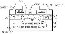
- This embodiment of the present inventionprovides an improved compromise between the on-state resistance and the breakdown voltage by enlarging the current conduction path at 24 in its active drain region 39 , the current path being ‘trumpet’ shaped, appearing as a ‘Y’-shape in the sectional view of FIG. 6 . As shown in FIG. 7 , this is achieved by providing peripheral regions 26 in the active drain region 39 extending beside the perimeter of the base-drain junction 18 , the peripheral regions being of higher dopant density than the rest of the second drain layer 10 . Moreover, intermediate regions 28 in the centre of the active drain region 39 are provided of lighter dopant density than the rest of the second drain layer 10 .
- the peripheral regions 26extend no deeper than the base regions 36 .
- the higher conductivity of the peripheral regions 26 and their action in enlarging the current conduction path 24 beside the perimeter 18 of the base-drain junctionenable the channel resistance R JFET to be reduced.
- any tendency of the higher dopant peripheral regions 26 to degrade the breakdown voltage of the deviceis more than compensated by reducing the dopant concentration in the intermediate regions 28 .
- the basic cell configurationis of the kind shown in FIGS. 1 to 3 , with four branches 80 of each individual basic cell extending in straight lines, merged base regions 36 in the vicinity of juxtaposed ends of the source regions of adjacent cells and the periphery 18 of the base-drain junction being rounded with the base region being concave.
- the perimeters 16 and 18 of the junctions and the peripheral regions 26are all generally ring shaped and concentric. This improves breakdown voltage by reducing electric field concentrations.
- the inventionis applicable to other configurations with different numbers of branches in each cell and even to stripe and other shaped cell configurations, such as those described in our European patent specification EP 1 387 408 and other documents referred to in the introduction to this specification.
- the lightly doped regionis arranged to be under a thicker ‘field oxide’ layer 30 where space charge extends in the off-state, which also helps to increase the breakdown voltage, whereas the insulating layer, which defines the spacing of the gate electrode 32 from the face 2 , is thinner at 31 in the vicinity of said junction perimeters than in areas adjacent said intermediate regions.
- a method of making a semiconductor device with such a ‘terraced’ gate oxide layer and self-aligned dopant regionsis described in an article by Ueda et al. in IEEE Transactions of Electronic Devices, vol. ED-31(no.4):416-20 1984, entitled “A new vertical double diffused MOSFET—the self-aligned terraced-gate MOSFET”, the teaching of which is incorporated herein by way of reference.
- FIGS. 8 and 9illustrate steps in an example of a method of making the semiconductor device shown in FIGS. 6 and 7 .
- the second drain layer 10is formed by epitaxial growth of semiconductor material on the first drain layer.
- the density of dopant in the second layer 10is reduced during the final stages of the step shown in FIG. 8 of growing semiconductor material epitaxially on said first drain layer, so as to produce a layer 27 of reduced dopant density, which will remain after forming the source, base and high dopant peripheral regions therein to provide the lightly doped regions 28 .
- the normal and thick oxide layers 31 and 30are then grown on the face 2 of the die.
- the gate electrodeis then formed over the oxide layers 30 and 31 by growing polysilicon and patterned by etching, using a photo-resist mask.
- Other features of the gate stacksuch as spacers for example, are added at different stages in the process.
- the features of the gate stackare used to define automatically-aligned masking for the steps of forming the source, base and high dopant peripheral regions 37 , 36 and 26 .
- the high dopant peripheral regions 26are formed by ion implant of the first conductivity type into the areas of the face 2 of the die left exposed by the oxide layers 30 and 31 .
- the base regions 36are then formed by diffusion of the opposite conductivity type and are then merged by subjecting the die to a high temperature.
- the source regions 37are formed by diffusion of the first conductivity type and the heavily doped regions 38 are formed by diffusion of the opposite conductivity type.
- the edge cells of the arraythat is to say the termination cells closest to the edges of the die, have a different configuration as shown in FIG. 10 , notably on their outer sides facing the adjacent die edge.
- each of the edge cellscomprises a source region 37 of the first conductivity type extending from the first face 2 and a base region 36 of the opposite conductivity type surrounding the source region at and below the first face.
- the base region 36forms with the source region 37 and second drain layer 10 respectively a base-source junction 12 and a base-drain junction 14 both extending to the first face 2 so as to define respective junction perimeters 16 and 18 thereat.
- the gate electrode 32insulated from the die, is disposed at the first face 2 extending over the base-source junction 12 and the base-drain junction 14 to form a conductive channel in the on-state of the device in the base region 36 , like in the basic cells.
- the edge cellhas a highly doped peripheral region 26 beside the perimeter 18 of the base-drain junction cooperating with the highly doped peripheral region 26 of the immediately adjacent basic cell in the array to form the trumpet shaped conduction path 24 and 22 .
- a highly doped peripheral region 26is also provided beside the perimeter 18 of the base-drain junction.
- the gate electrode 32extends over and beyond at least part of the perimeters 16 and 18 of the base-source junction and the base-drain junction towards the adjacent edge of the die.
- the second drain layer 10includes a region 27 of reduced dopant density that extends from the highly doped peripheral region 26 beyond the gate electrode right to the adjacent edge of the die.
- the thicker oxide layer 30extends out to the edge of the die on the outer side of the edge cells. These features of the outer side of the edge cells maintain the breakdown voltage of the device that otherwise might be degraded in these outer sides.
Landscapes
- Insulated Gate Type Field-Effect Transistor (AREA)
Abstract
Description
Claims (10)
Applications Claiming Priority (1)
| Application Number | Priority Date | Filing Date | Title |
|---|---|---|---|
| PCT/EP2005/010049WO2007016969A1 (en) | 2005-07-25 | 2005-07-25 | Power semiconductor device and method of manufacturing a power semiconductor device |
Publications (2)
| Publication Number | Publication Date |
|---|---|
| US20080217657A1 US20080217657A1 (en) | 2008-09-11 |
| US7800135B2true US7800135B2 (en) | 2010-09-21 |
Family
ID=36120118
Family Applications (1)
| Application Number | Title | Priority Date | Filing Date |
|---|---|---|---|
| US11/996,681Active2026-03-22US7800135B2 (en) | 2005-07-25 | 2005-07-25 | Power semiconductor device and method of manufacturing a power semiconductor device |
Country Status (3)
| Country | Link |
|---|---|
| US (1) | US7800135B2 (en) |
| EP (1) | EP1911097B1 (en) |
| WO (1) | WO2007016969A1 (en) |
Cited By (1)
| Publication number | Priority date | Publication date | Assignee | Title |
|---|---|---|---|---|
| US20100314695A1 (en)* | 2009-06-10 | 2010-12-16 | International Rectifier Corporation | Self-aligned vertical group III-V transistor and method for fabricated same |
Citations (12)
| Publication number | Priority date | Publication date | Assignee | Title |
|---|---|---|---|---|
| US4376286A (en) | 1978-10-13 | 1983-03-08 | International Rectifier Corporation | High power MOSFET with low on-resistance and high breakdown voltage |
| US4593302A (en) | 1980-08-18 | 1986-06-03 | International Rectifier Corporation | Process for manufacture of high power MOSFET with laterally distributed high carrier density beneath the gate oxide |
| EP0335750A2 (en) | 1988-04-01 | 1989-10-04 | Nec Corporation | Vertical power mosfet having high withstand voltage and high switching speed |
| US5075739A (en) | 1990-01-02 | 1991-12-24 | Motorola, Inc. | High voltage planar edge termination using a punch-through retarding implant and floating field plates |
| EP0583911A1 (en) | 1992-08-04 | 1994-02-23 | Siliconix Incorporated | MOS transistor channel structure |
| EP0655787A2 (en) | 1993-11-22 | 1995-05-31 | Motorola, Inc. | Transistor with common base region |
| US5703389A (en) | 1995-02-24 | 1997-12-30 | Motorola, Inc. | Vertical IGFET configuration having low on-resistance and method |
| US6144067A (en) | 1998-11-23 | 2000-11-07 | International Rectifier Corp. | Strip gate poly structure for increased channel width and reduced gate resistance |
| WO2001031711A2 (en) | 1999-10-22 | 2001-05-03 | Semiconductor Components Industries, L.L.C. | Vertical insulated gate field-effect device and method of making the same |
| WO2001031709A1 (en) | 1999-10-22 | 2001-05-03 | Semiconductor Components Industries, L.L.C. | Semiconductor device with a single base region and method therefor |
| US20030057478A1 (en) | 2001-09-12 | 2003-03-27 | Chong-Man Yun | Mos-gated power semiconductor device |
| WO2003107432A1 (en) | 2002-06-12 | 2003-12-24 | Motorola Inc | Power semiconductor device and method of manufacturing the same |
- 2005
- 2005-07-25WOPCT/EP2005/010049patent/WO2007016969A1/ennot_activeApplication Discontinuation
- 2005-07-25USUS11/996,681patent/US7800135B2/enactiveActive
- 2005-07-25EPEP05789338.0Apatent/EP1911097B1/ennot_activeCeased
Patent Citations (16)
| Publication number | Priority date | Publication date | Assignee | Title |
|---|---|---|---|---|
| US4376286B1 (en) | 1978-10-13 | 1993-07-20 | Int Rectifier Corp | |
| US4376286A (en) | 1978-10-13 | 1983-03-08 | International Rectifier Corporation | High power MOSFET with low on-resistance and high breakdown voltage |
| US4593302B1 (en) | 1980-08-18 | 1998-02-03 | Int Rectifier Corp | Process for manufacture of high power mosfet laterally distributed high carrier density beneath the gate oxide |
| US4593302A (en) | 1980-08-18 | 1986-06-03 | International Rectifier Corporation | Process for manufacture of high power MOSFET with laterally distributed high carrier density beneath the gate oxide |
| EP0335750A2 (en) | 1988-04-01 | 1989-10-04 | Nec Corporation | Vertical power mosfet having high withstand voltage and high switching speed |
| US5075739A (en) | 1990-01-02 | 1991-12-24 | Motorola, Inc. | High voltage planar edge termination using a punch-through retarding implant and floating field plates |
| EP0583911A1 (en) | 1992-08-04 | 1994-02-23 | Siliconix Incorporated | MOS transistor channel structure |
| EP0827209A1 (en) | 1993-11-22 | 1998-03-04 | Motorola, Inc. | Gate layout of a transistor with common base region |
| EP0655787A2 (en) | 1993-11-22 | 1995-05-31 | Motorola, Inc. | Transistor with common base region |
| US5703389A (en) | 1995-02-24 | 1997-12-30 | Motorola, Inc. | Vertical IGFET configuration having low on-resistance and method |
| US6144067A (en) | 1998-11-23 | 2000-11-07 | International Rectifier Corp. | Strip gate poly structure for increased channel width and reduced gate resistance |
| WO2001031711A2 (en) | 1999-10-22 | 2001-05-03 | Semiconductor Components Industries, L.L.C. | Vertical insulated gate field-effect device and method of making the same |
| WO2001031709A1 (en) | 1999-10-22 | 2001-05-03 | Semiconductor Components Industries, L.L.C. | Semiconductor device with a single base region and method therefor |
| US20030057478A1 (en) | 2001-09-12 | 2003-03-27 | Chong-Man Yun | Mos-gated power semiconductor device |
| WO2003107432A1 (en) | 2002-06-12 | 2003-12-24 | Motorola Inc | Power semiconductor device and method of manufacturing the same |
| EP1387408A1 (en) | 2002-06-12 | 2004-02-04 | Motorola, Inc. | Power semiconductor device and method of manufacturing the same |
Non-Patent Citations (1)
| Title |
|---|
| "A New Vertical Double Diffused MOSFET-The Self-Aligned Terraced-Gate MOSFET" IEEE Transactions on Electron Devices, Apr. 1984. |
Cited By (1)
| Publication number | Priority date | Publication date | Assignee | Title |
|---|---|---|---|---|
| US20100314695A1 (en)* | 2009-06-10 | 2010-12-16 | International Rectifier Corporation | Self-aligned vertical group III-V transistor and method for fabricated same |
Also Published As
| Publication number | Publication date |
|---|---|
| EP1911097B1 (en) | 2018-04-25 |
| US20080217657A1 (en) | 2008-09-11 |
| EP1911097A1 (en) | 2008-04-16 |
| WO2007016969A1 (en) | 2007-02-15 |
Similar Documents
| Publication | Publication Date | Title |
|---|---|---|
| US5589405A (en) | Method for fabricating VDMOS transistor with improved breakdown characteristics | |
| US7663186B2 (en) | Semiconductor device | |
| US6566690B2 (en) | Single feature size MOS technology power device | |
| US20090206913A1 (en) | Edge Termination with Improved Breakdown Voltage | |
| US5528063A (en) | Conductive-overlaid self-aligned MOS-gated semiconductor devices | |
| US20030057478A1 (en) | Mos-gated power semiconductor device | |
| CN1552101B (en) | Recessed DMOS Transistor with Lightly Doped Source Structure | |
| US20020079521A1 (en) | Surface breakdown reduction by internal field rings and multiple poly field plates in power LDMOSFET | |
| US6548864B2 (en) | High density MOS technology power device | |
| US8004049B2 (en) | Power semiconductor device | |
| JP4550182B2 (en) | High density MOS technology power device structure | |
| US6492663B1 (en) | Universal source geometry for MOS-gated power devices | |
| US7432145B2 (en) | Power semiconductor device with a base region and method of manufacturing same | |
| US7800135B2 (en) | Power semiconductor device and method of manufacturing a power semiconductor device | |
| EP0823735A1 (en) | MOS-technology power device | |
| KR100949139B1 (en) | Trench dmos transistor having improved trench structure | |
| US6635926B2 (en) | Field effect transistor with high withstand voltage and low resistance | |
| CN101228636B (en) | Power semiconductor device as well as method for making the same | |
| JPS6218767A (en) | Vertical semiconductor device and its manufacturing method | |
| JP2003309129A (en) | Method for manufacturing semiconductor device |
Legal Events
| Date | Code | Title | Description |
|---|---|---|---|
| AS | Assignment | Owner name:FREESCALE SEMICONDUCTOR, INC., TEXAS Free format text:ASSIGNMENT OF ASSIGNORS INTEREST;ASSIGNORS:REYNES, JEAN-MICHEL;ALVES, STEPHANE;DERAM, ALAIN J.;AND OTHERS;REEL/FRAME:020409/0890;SIGNING DATES FROM 20080104 TO 20080107 Owner name:FREESCALE SEMICONDUCTOR, INC., TEXAS Free format text:ASSIGNMENT OF ASSIGNORS INTEREST;ASSIGNORS:REYNES, JEAN-MICHEL;ALVES, STEPHANE;DERAM, ALAIN J.;AND OTHERS;SIGNING DATES FROM 20080104 TO 20080107;REEL/FRAME:020409/0890 | |
| AS | Assignment | Owner name:CITIBANK, N.A., NEW YORK Free format text:SECURITY AGREEMENT;ASSIGNOR:FREESCALE SEMICONDUCTOR, INC.;REEL/FRAME:021194/0593 Effective date:20080425 | |
| AS | Assignment | Owner name:CITIBANK, N.A.,NEW YORK Free format text:SECURITY AGREEMENT;ASSIGNOR:FREESCALE SEMICONDUCTOR, INC.;REEL/FRAME:024085/0001 Effective date:20100219 Owner name:CITIBANK, N.A., NEW YORK Free format text:SECURITY AGREEMENT;ASSIGNOR:FREESCALE SEMICONDUCTOR, INC.;REEL/FRAME:024085/0001 Effective date:20100219 | |
| AS | Assignment | Owner name:CITIBANK, N.A., AS COLLATERAL AGENT,NEW YORK Free format text:SECURITY AGREEMENT;ASSIGNOR:FREESCALE SEMICONDUCTOR, INC.;REEL/FRAME:024397/0001 Effective date:20100413 Owner name:CITIBANK, N.A., AS COLLATERAL AGENT, NEW YORK Free format text:SECURITY AGREEMENT;ASSIGNOR:FREESCALE SEMICONDUCTOR, INC.;REEL/FRAME:024397/0001 Effective date:20100413 | |
| STCF | Information on status: patent grant | Free format text:PATENTED CASE | |
| AS | Assignment | Owner name:CITIBANK, N.A., AS NOTES COLLATERAL AGENT, NEW YORK Free format text:SECURITY AGREEMENT;ASSIGNOR:FREESCALE SEMICONDUCTOR, INC.;REEL/FRAME:030633/0424 Effective date:20130521 Owner name:CITIBANK, N.A., AS NOTES COLLATERAL AGENT, NEW YOR Free format text:SECURITY AGREEMENT;ASSIGNOR:FREESCALE SEMICONDUCTOR, INC.;REEL/FRAME:030633/0424 Effective date:20130521 | |
| AS | Assignment | Owner name:CITIBANK, N.A., AS NOTES COLLATERAL AGENT, NEW YORK Free format text:SECURITY AGREEMENT;ASSIGNOR:FREESCALE SEMICONDUCTOR, INC.;REEL/FRAME:031591/0266 Effective date:20131101 Owner name:CITIBANK, N.A., AS NOTES COLLATERAL AGENT, NEW YOR Free format text:SECURITY AGREEMENT;ASSIGNOR:FREESCALE SEMICONDUCTOR, INC.;REEL/FRAME:031591/0266 Effective date:20131101 | |
| FPAY | Fee payment | Year of fee payment:4 | |
| AS | Assignment | Owner name:FREESCALE SEMICONDUCTOR, INC., TEXAS Free format text:PATENT RELEASE;ASSIGNOR:CITIBANK, N.A., AS COLLATERAL AGENT;REEL/FRAME:037354/0688 Effective date:20151207 Owner name:FREESCALE SEMICONDUCTOR, INC., TEXAS Free format text:PATENT RELEASE;ASSIGNOR:CITIBANK, N.A., AS COLLATERAL AGENT;REEL/FRAME:037356/0553 Effective date:20151207 Owner name:FREESCALE SEMICONDUCTOR, INC., TEXAS Free format text:PATENT RELEASE;ASSIGNOR:CITIBANK, N.A., AS COLLATERAL AGENT;REEL/FRAME:037356/0143 Effective date:20151207 | |
| AS | Assignment | Owner name:MORGAN STANLEY SENIOR FUNDING, INC., MARYLAND Free format text:ASSIGNMENT AND ASSUMPTION OF SECURITY INTEREST IN PATENTS;ASSIGNOR:CITIBANK, N.A.;REEL/FRAME:037486/0517 Effective date:20151207 | |
| AS | Assignment | Owner name:MORGAN STANLEY SENIOR FUNDING, INC., MARYLAND Free format text:ASSIGNMENT AND ASSUMPTION OF SECURITY INTEREST IN PATENTS;ASSIGNOR:CITIBANK, N.A.;REEL/FRAME:037518/0292 Effective date:20151207 | |
| AS | Assignment | Owner name:MORGAN STANLEY SENIOR FUNDING, INC., MARYLAND Free format text:SECURITY AGREEMENT SUPPLEMENT;ASSIGNOR:NXP B.V.;REEL/FRAME:038017/0058 Effective date:20160218 | |
| AS | Assignment | Owner name:MORGAN STANLEY SENIOR FUNDING, INC., MARYLAND Free format text:SUPPLEMENT TO THE SECURITY AGREEMENT;ASSIGNOR:FREESCALE SEMICONDUCTOR, INC.;REEL/FRAME:039138/0001 Effective date:20160525 | |
| AS | Assignment | Owner name:MORGAN STANLEY SENIOR FUNDING, INC., MARYLAND Free format text:CORRECTIVE ASSIGNMENT TO CORRECT THE REMOVE APPLICATION 12092129 PREVIOUSLY RECORDED ON REEL 038017 FRAME 0058. ASSIGNOR(S) HEREBY CONFIRMS THE SECURITY AGREEMENT SUPPLEMENT;ASSIGNOR:NXP B.V.;REEL/FRAME:039361/0212 Effective date:20160218 | |
| AS | Assignment | Owner name:NXP, B.V., F/K/A FREESCALE SEMICONDUCTOR, INC., NETHERLANDS Free format text:RELEASE BY SECURED PARTY;ASSIGNOR:MORGAN STANLEY SENIOR FUNDING, INC.;REEL/FRAME:040925/0001 Effective date:20160912 Owner name:NXP, B.V., F/K/A FREESCALE SEMICONDUCTOR, INC., NE Free format text:RELEASE BY SECURED PARTY;ASSIGNOR:MORGAN STANLEY SENIOR FUNDING, INC.;REEL/FRAME:040925/0001 Effective date:20160912 | |
| AS | Assignment | Owner name:NXP B.V., NETHERLANDS Free format text:RELEASE BY SECURED PARTY;ASSIGNOR:MORGAN STANLEY SENIOR FUNDING, INC.;REEL/FRAME:040928/0001 Effective date:20160622 | |
| AS | Assignment | Owner name:NXP USA, INC., TEXAS Free format text:CHANGE OF NAME;ASSIGNOR:FREESCALE SEMICONDUCTOR INC.;REEL/FRAME:040652/0180 Effective date:20161107 | |
| AS | Assignment | Owner name:NXP USA, INC., TEXAS Free format text:CORRECTIVE ASSIGNMENT TO CORRECT THE NATURE OF CONVEYANCE LISTED CHANGE OF NAME SHOULD BE MERGER AND CHANGE PREVIOUSLY RECORDED AT REEL: 040652 FRAME: 0180. ASSIGNOR(S) HEREBY CONFIRMS THE MERGER AND CHANGE OF NAME;ASSIGNOR:FREESCALE SEMICONDUCTOR INC.;REEL/FRAME:041354/0148 Effective date:20161107 | |
| AS | Assignment | Owner name:MORGAN STANLEY SENIOR FUNDING, INC., MARYLAND Free format text:CORRECTIVE ASSIGNMENT TO CORRECT THE REMOVE PATENTS 8108266 AND 8062324 AND REPLACE THEM WITH 6108266 AND 8060324 PREVIOUSLY RECORDED ON REEL 037518 FRAME 0292. ASSIGNOR(S) HEREBY CONFIRMS THE ASSIGNMENT AND ASSUMPTION OF SECURITY INTEREST IN PATENTS;ASSIGNOR:CITIBANK, N.A.;REEL/FRAME:041703/0536 Effective date:20151207 | |
| AS | Assignment | Owner name:MORGAN STANLEY SENIOR FUNDING, INC., MARYLAND Free format text:CORRECTIVE ASSIGNMENT TO CORRECT THE REMOVE APPLICATION 12681366 PREVIOUSLY RECORDED ON REEL 039361 FRAME 0212. ASSIGNOR(S) HEREBY CONFIRMS THE SECURITY AGREEMENT SUPPLEMENT;ASSIGNOR:NXP B.V.;REEL/FRAME:042762/0145 Effective date:20160218 Owner name:MORGAN STANLEY SENIOR FUNDING, INC., MARYLAND Free format text:CORRECTIVE ASSIGNMENT TO CORRECT THE REMOVE APPLICATION 12681366 PREVIOUSLY RECORDED ON REEL 038017 FRAME 0058. ASSIGNOR(S) HEREBY CONFIRMS THE SECURITY AGREEMENT SUPPLEMENT;ASSIGNOR:NXP B.V.;REEL/FRAME:042985/0001 Effective date:20160218 | |
| MAFP | Maintenance fee payment | Free format text:PAYMENT OF MAINTENANCE FEE, 8TH YEAR, LARGE ENTITY (ORIGINAL EVENT CODE: M1552) Year of fee payment:8 | |
| AS | Assignment | Owner name:SHENZHEN XINGUODU TECHNOLOGY CO., LTD., CHINA Free format text:CORRECTIVE ASSIGNMENT TO CORRECT THE TO CORRECT THE APPLICATION NO. FROM 13,883,290 TO 13,833,290 PREVIOUSLY RECORDED ON REEL 041703 FRAME 0536. ASSIGNOR(S) HEREBY CONFIRMS THE THE ASSIGNMENT AND ASSUMPTION OF SECURITYINTEREST IN PATENTS.;ASSIGNOR:MORGAN STANLEY SENIOR FUNDING, INC.;REEL/FRAME:048734/0001 Effective date:20190217 | |
| AS | Assignment | Owner name:NXP B.V., NETHERLANDS Free format text:RELEASE BY SECURED PARTY;ASSIGNOR:MORGAN STANLEY SENIOR FUNDING, INC.;REEL/FRAME:050744/0097 Effective date:20190903 Owner name:NXP B.V., NETHERLANDS Free format text:RELEASE BY SECURED PARTY;ASSIGNOR:MORGAN STANLEY SENIOR FUNDING, INC.;REEL/FRAME:050745/0001 Effective date:20190903 | |
| AS | Assignment | Owner name:MORGAN STANLEY SENIOR FUNDING, INC., MARYLAND Free format text:CORRECTIVE ASSIGNMENT TO CORRECT THE REMOVE APPLICATION 12298143 PREVIOUSLY RECORDED ON REEL 042985 FRAME 0001. ASSIGNOR(S) HEREBY CONFIRMS THE SECURITY AGREEMENT SUPPLEMENT;ASSIGNOR:NXP B.V.;REEL/FRAME:051029/0001 Effective date:20160218 Owner name:MORGAN STANLEY SENIOR FUNDING, INC., MARYLAND Free format text:CORRECTIVE ASSIGNMENT TO CORRECT THE REMOVE APPLICATION 12298143 PREVIOUSLY RECORDED ON REEL 042762 FRAME 0145. ASSIGNOR(S) HEREBY CONFIRMS THE SECURITY AGREEMENT SUPPLEMENT;ASSIGNOR:NXP B.V.;REEL/FRAME:051145/0184 Effective date:20160218 Owner name:MORGAN STANLEY SENIOR FUNDING, INC., MARYLAND Free format text:CORRECTIVE ASSIGNMENT TO CORRECT THE REMOVE APPLICATION 12298143 PREVIOUSLY RECORDED ON REEL 039361 FRAME 0212. ASSIGNOR(S) HEREBY CONFIRMS THE SECURITY AGREEMENT SUPPLEMENT;ASSIGNOR:NXP B.V.;REEL/FRAME:051029/0387 Effective date:20160218 Owner name:MORGAN STANLEY SENIOR FUNDING, INC., MARYLAND Free format text:CORRECTIVE ASSIGNMENT TO CORRECT THE REMOVE APPLICATION 12298143 PREVIOUSLY RECORDED ON REEL 038017 FRAME 0058. ASSIGNOR(S) HEREBY CONFIRMS THE SECURITY AGREEMENT SUPPLEMENT;ASSIGNOR:NXP B.V.;REEL/FRAME:051030/0001 Effective date:20160218 Owner name:MORGAN STANLEY SENIOR FUNDING, INC., MARYLAND Free format text:CORRECTIVE ASSIGNMENT TO CORRECT THE REMOVE APPLICATION12298143 PREVIOUSLY RECORDED ON REEL 039361 FRAME 0212. ASSIGNOR(S) HEREBY CONFIRMS THE SECURITY AGREEMENT SUPPLEMENT;ASSIGNOR:NXP B.V.;REEL/FRAME:051029/0387 Effective date:20160218 Owner name:MORGAN STANLEY SENIOR FUNDING, INC., MARYLAND Free format text:CORRECTIVE ASSIGNMENT TO CORRECT THE REMOVE APPLICATION12298143 PREVIOUSLY RECORDED ON REEL 042985 FRAME 0001. ASSIGNOR(S) HEREBY CONFIRMS THE SECURITY AGREEMENT SUPPLEMENT;ASSIGNOR:NXP B.V.;REEL/FRAME:051029/0001 Effective date:20160218 Owner name:MORGAN STANLEY SENIOR FUNDING, INC., MARYLAND Free format text:CORRECTIVE ASSIGNMENT TO CORRECT THE REMOVE APPLICATION12298143 PREVIOUSLY RECORDED ON REEL 042762 FRAME 0145. ASSIGNOR(S) HEREBY CONFIRMS THE SECURITY AGREEMENT SUPPLEMENT;ASSIGNOR:NXP B.V.;REEL/FRAME:051145/0184 Effective date:20160218 | |
| AS | Assignment | Owner name:MORGAN STANLEY SENIOR FUNDING, INC., MARYLAND Free format text:CORRECTIVE ASSIGNMENT TO CORRECT THE REMOVE APPLICATION11759915 AND REPLACE IT WITH APPLICATION 11759935 PREVIOUSLY RECORDED ON REEL 037486 FRAME 0517. ASSIGNOR(S) HEREBY CONFIRMS THE ASSIGNMENT AND ASSUMPTION OF SECURITYINTEREST IN PATENTS;ASSIGNOR:CITIBANK, N.A.;REEL/FRAME:053547/0421 Effective date:20151207 | |
| AS | Assignment | Owner name:NXP B.V., NETHERLANDS Free format text:CORRECTIVE ASSIGNMENT TO CORRECT THE REMOVEAPPLICATION 11759915 AND REPLACE IT WITH APPLICATION11759935 PREVIOUSLY RECORDED ON REEL 040928 FRAME 0001. ASSIGNOR(S) HEREBY CONFIRMS THE RELEASE OF SECURITYINTEREST;ASSIGNOR:MORGAN STANLEY SENIOR FUNDING, INC.;REEL/FRAME:052915/0001 Effective date:20160622 | |
| AS | Assignment | Owner name:NXP, B.V. F/K/A FREESCALE SEMICONDUCTOR, INC., NETHERLANDS Free format text:CORRECTIVE ASSIGNMENT TO CORRECT THE REMOVEAPPLICATION 11759915 AND REPLACE IT WITH APPLICATION11759935 PREVIOUSLY RECORDED ON REEL 040925 FRAME 0001. ASSIGNOR(S) HEREBY CONFIRMS THE RELEASE OF SECURITYINTEREST;ASSIGNOR:MORGAN STANLEY SENIOR FUNDING, INC.;REEL/FRAME:052917/0001 Effective date:20160912 | |
| MAFP | Maintenance fee payment | Free format text:PAYMENT OF MAINTENANCE FEE, 12TH YEAR, LARGE ENTITY (ORIGINAL EVENT CODE: M1553); ENTITY STATUS OF PATENT OWNER: LARGE ENTITY Year of fee payment:12 |