US7800121B2 - Light emitting diode component - Google Patents
Light emitting diode componentDownload PDFInfo
- Publication number
- US7800121B2 US7800121B2US11/312,268US31226805AUS7800121B2US 7800121 B2US7800121 B2US 7800121B2US 31226805 AUS31226805 AUS 31226805AUS 7800121 B2US7800121 B2US 7800121B2
- Authority
- US
- United States
- Prior art keywords
- light
- light emitting
- phosphor
- printed circuit
- circuit board
- Prior art date
- Legal status (The legal status is an assumption and is not a legal conclusion. Google has not performed a legal analysis and makes no representation as to the accuracy of the status listed.)
- Expired - Lifetime, expires
Links
Images


Classifications
- H—ELECTRICITY
- H01—ELECTRIC ELEMENTS
- H01L—SEMICONDUCTOR DEVICES NOT COVERED BY CLASS H10
- H01L25/00—Assemblies consisting of a plurality of semiconductor or other solid state devices
- H01L25/03—Assemblies consisting of a plurality of semiconductor or other solid state devices all the devices being of a type provided for in a single subclass of subclasses H10B, H10D, H10F, H10H, H10K or H10N, e.g. assemblies of rectifier diodes
- H01L25/04—Assemblies consisting of a plurality of semiconductor or other solid state devices all the devices being of a type provided for in a single subclass of subclasses H10B, H10D, H10F, H10H, H10K or H10N, e.g. assemblies of rectifier diodes the devices not having separate containers
- H01L25/075—Assemblies consisting of a plurality of semiconductor or other solid state devices all the devices being of a type provided for in a single subclass of subclasses H10B, H10D, H10F, H10H, H10K or H10N, e.g. assemblies of rectifier diodes the devices not having separate containers the devices being of a type provided for in group H10H20/00
- H01L25/0753—Assemblies consisting of a plurality of semiconductor or other solid state devices all the devices being of a type provided for in a single subclass of subclasses H10B, H10D, H10F, H10H, H10K or H10N, e.g. assemblies of rectifier diodes the devices not having separate containers the devices being of a type provided for in group H10H20/00 the devices being arranged next to each other
- H—ELECTRICITY
- H10—SEMICONDUCTOR DEVICES; ELECTRIC SOLID-STATE DEVICES NOT OTHERWISE PROVIDED FOR
- H10H—INORGANIC LIGHT-EMITTING SEMICONDUCTOR DEVICES HAVING POTENTIAL BARRIERS
- H10H20/00—Individual inorganic light-emitting semiconductor devices having potential barriers, e.g. light-emitting diodes [LED]
- H10H20/80—Constructional details
- H10H20/85—Packages
- H10H20/851—Wavelength conversion means
- H10H20/8515—Wavelength conversion means not being in contact with the bodies
- F—MECHANICAL ENGINEERING; LIGHTING; HEATING; WEAPONS; BLASTING
- F21—LIGHTING
- F21K—NON-ELECTRIC LIGHT SOURCES USING LUMINESCENCE; LIGHT SOURCES USING ELECTROCHEMILUMINESCENCE; LIGHT SOURCES USING CHARGES OF COMBUSTIBLE MATERIAL; LIGHT SOURCES USING SEMICONDUCTOR DEVICES AS LIGHT-GENERATING ELEMENTS; LIGHT SOURCES NOT OTHERWISE PROVIDED FOR
- F21K9/00—Light sources using semiconductor devices as light-generating elements, e.g. using light-emitting diodes [LED] or lasers
- F21K9/60—Optical arrangements integrated in the light source, e.g. for improving the colour rendering index or the light extraction
- F21K9/68—Details of reflectors forming part of the light source
- F—MECHANICAL ENGINEERING; LIGHTING; HEATING; WEAPONS; BLASTING
- F21—LIGHTING
- F21V—FUNCTIONAL FEATURES OR DETAILS OF LIGHTING DEVICES OR SYSTEMS THEREOF; STRUCTURAL COMBINATIONS OF LIGHTING DEVICES WITH OTHER ARTICLES, NOT OTHERWISE PROVIDED FOR
- F21V23/00—Arrangement of electric circuit elements in or on lighting devices
- H—ELECTRICITY
- H01—ELECTRIC ELEMENTS
- H01L—SEMICONDUCTOR DEVICES NOT COVERED BY CLASS H10
- H01L2224/00—Indexing scheme for arrangements for connecting or disconnecting semiconductor or solid-state bodies and methods related thereto as covered by H01L24/00
- H01L2224/01—Means for bonding being attached to, or being formed on, the surface to be connected, e.g. chip-to-package, die-attach, "first-level" interconnects; Manufacturing methods related thereto
- H01L2224/42—Wire connectors; Manufacturing methods related thereto
- H01L2224/47—Structure, shape, material or disposition of the wire connectors after the connecting process
- H01L2224/48—Structure, shape, material or disposition of the wire connectors after the connecting process of an individual wire connector
- H01L2224/4805—Shape
- H01L2224/4809—Loop shape
- H01L2224/48091—Arched
- H—ELECTRICITY
- H01—ELECTRIC ELEMENTS
- H01L—SEMICONDUCTOR DEVICES NOT COVERED BY CLASS H10
- H01L2924/00—Indexing scheme for arrangements or methods for connecting or disconnecting semiconductor or solid-state bodies as covered by H01L24/00
- H01L2924/013—Alloys
- H01L2924/0132—Binary Alloys
- H01L2924/01322—Eutectic Alloys, i.e. obtained by a liquid transforming into two solid phases
Definitions
- the present inventionrelates to the lighting arts. It especially relates to single-chip and multiple-chip light emitting diode components and methods for making same, and will be described with particular reference thereto.
- the inventionapplies to light emitting packages generally, and is applicable in packaging monolithic light emitting diode array dice, edge-emitting laser dice, vertical cavity light emitting dice or monolithic laser array dice, organic light emitting devices or organic light emitting array devices, and the like.
- the inventive light emitting packages and componentswill find application in substantially any application that employs one or more light sources.
- Light emitting diode componentsprovide illumination in small, rugged, reliable packages.
- Light emitting diodeshave been developed in many colors spanning the visible spectrum and extending into the infrared and ultraviolet. While each light emitting diode typically emits light in a narrow spectral range, primary color light emitting diodes can be combined to emit white light. In another approach for generating white light, light from a blue, violet, or ultraviolet light emitting diode is coupled with a suitable phosphor to produce white light. Other colors can similarly be generated by suitable selection of light emitting die components, phosphors, and combinations of die components and phosphors.
- light emitting diode components or packagesrelate to light output intensity.
- Early light emitting diodeshad low light output intensities and were generally not competitive with incandescent and fluorescent light sources. Improvements in crystal growth, device fabrication, packaging methods, phosphor materials, and the like have substantially improved the light output intensities of modern light emitting diode packages. However, improvements in light output intensities are still being sought.
- a typical single-chip packagemay include, for example, a light emitting diode die, a lead frame, an encapsulant disposed over the light emitting diode die and a portion of the lead frame, and a phosphor embedded in the encapsulant.
- Multiple chip packagesgenerally further increase complexity.
- One example of such a multiple chip packageis disclosed in Lowery, U.S. Pat. No. 6,504,301, which shows various arrangements involving generally wire-bonded interconnection of a plurality of light emitting dice disposed on a support placed in a housing including a cylindrical casing and a fluorescent plate.
- a similar multiple chip packageis disclosed in Baretz et al., U.S. Pat. No. 6,600,175.
- Baretzdiscloses a phosphor contained in an encapsulant disposed inside the housing,
- the complexity of multiple chip packages such as those of Lowery and Baretzcan adversely impact manufacturability, reliability, and manufacturing costs.
- Performance of packages employing phosphor wavelength conversion of ultraviolet or short-wavelength visible lighttypically degrades over time due to discoloration or other degradation of the encapsulant or other materials caused by the ultraviolet or short-wavelength visible light irradiation.
- a typical light emitting diode packageis configured as a discrete electronic component and includes a lead frame or other electronic component mounting arrangement designed for solder connection. This approach is suitable for applications such as visual power indicators.
- the light emitting diode packagewould desirably be used in a manner more analogous to a light bulb, fluorescent lighting tube, halogen bulb, or so forth, rather than as a discrete electronic component.
- the light emitting diode package for illumination applicationsshould be readily connectable with existing illumination fixtures such as Edison sockets, track lighting fixtures, or so forth.
- existing illumination fixturessuch as Edison sockets, track lighting fixtures, or so forth.
- Such plug-in fixture compatibilityis, however, hampered by the typically high voltage and/or high frequency electrical power supplied by such fixtures, which is not conducive to powering low-voltage light emitting diode devices.
- light output qualityAnother issue with using light emitting diode packages for illumination is light output quality.
- light emitting diode packagesemploy several light emitting chips so as to produce high light intensity, a problem arises in that the output consists of several approximate point light sources corresponding to the several chips. This pixelated spatial distribution of light is problematic for illumination applications.
- Spectral light output qualitycan also be an issue when using light emitting diode packages for white illumination.
- different applicationsmay call for different color rendering index (CRI) values.
- CRIcolor rendering index
- Obtaining white light or substantially white light with a desired (usually high) CRI value in a commercially practical manneris difficult.
- Existing cost-effective “white” phosphor compositionssometimes have relatively low CRI values.
- the present inventioncontemplates improved apparatuses and methods that overcome the above-mentioned limitations and others.
- a light emitting packageis disclosed.
- a printed circuit boardsupports at least one light emitting die and has at least two electrical terminals.
- Printed circuitry of the printed circuit boardconnects the at least one light emitting die with the at least two electrical terminals to provide power thereto.
- a light transmissive coveris disposed over the at least one light emitting die but not over the at least two electrical terminals.
- the coverhas an open end defining a cover perimeter connected with the printed circuit board.
- An inside surface of the cover together with the printed circuit boarddefines an interior volume containing the at least one light emitting die.
- An encapsulantis disposed in the interior volume and covers at least the light emitting die.
- a light emitting packageis disclosed.
- a supporthas at least one light emitting die disposed thereon.
- a glass coveris disposed on the support over the at least one light emitting die.
- the glass cover and the supportcooperatively define an interior volume containing the at least one light emitting die.
- An encapsulantis disposed in the interior volume and encapsulates the at least one light emitting die.
- a light emitting packageis disclosed.
- a supporthas at least one light emitting die disposed thereon.
- a single piece light transmissive coveris disposed on the support over the at least one light emitting die.
- the single piece cover and the supportcooperatively define a substantially closed interior volume containing the at least one light emitting die.
- An encapsulantis disposed in the interior volume and encapsulates the at least one light emitting die.
- a methodfor making a light emitting package. At least one light emitting die is electrically and mechanically connected to a printed circuit board. A light transmissive cover is secured to the printed circuit board. The light transmissive cover covers the at least one light emitting die. The secured light transmissive cover and the printed circuit board cooperatively define an interior volume. An encapsulant is disposed in the interior volume.
- a methodfor disposing of a phosphor on a surface.
- An adhesiveis disposed on the surface.
- a phosphor powderis applied to the adhesive.
- the adhesiveis hardened.
- a lighting packageis disclosed.
- a printed circuit boardsupports at least one light emitting die.
- a light transmissive coveris disposed over the at least one light emitting die.
- At least one phosphor compositioncomprising at least one phosphor compound is disposed on or inside of the light transmissive cover. The at least one phosphor composition outputs converted light responsive to irradiation by the at least one light emitting die.
- a lighting packageis disclosed.
- a printed circuit boardsupports at least one light emitting die.
- a light transmissive coveris disposed over the at least one light emitting die.
- An encapsulantsubstantially fills an interior volume defined by the light-transmissive cover and the printed circuit board.
- a lighting packageis disclosed.
- a printed circuit boardsupports at least one light emitting die.
- a light transmissive coveris disposed over the at least one light emitting die.
- Electrical power-conditioning circuitryis disposed on the printed circuit board and is configured to condition received input power to energize the supported at least one light emitting die.
- the inventionmay take form in various components and arrangements of components, and in various process operations and arrangements of process operations.
- the drawingsare only for purposes of illustrating preferred embodiments and are not to be construed as limiting the invention.
- FIG. 1shows a perspective view of a lighting component or package.
- FIG. 2shows a perspective view of the printed circuit board of the lighting package of FIG. 1 with the light emitting dice or chips and associated electrical components disposed thereon.
- FIG. 3shows a perspective view of the lighting component or package of FIG. 1 with a portion of the light transmissive cover removed to show internal elements of the lighting package.
- FIG. 4diagrams an example process for manufacturing the lighting package of FIG. 1 .
- FIG. 5shows a perspective view of another lighting component or package having backside electrical terminals.
- FIG. 6shows CRI tuning using a first phosphor composition having phosphor compounds (A,B,C) and a second phosphor composition having phosphor compounds (B,C,D).
- FIG. 7shows a high CRI spectrum achievable using the CRI tuning of FIG. 6 .
- FIG. 8shows a perspective view of another lighting component or package having light emitting chips arranged in a long double-row.
- a portion of the light transmissive coveris removed to show some of the light emitting dice or chips and other internal components.
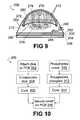
- FIG. 9shows a perspective view of another lighting component or package, in which the light emitting dice and the phosphor are encapsulated by separate encapsulants.
- a portion of the light transmissive coverremoved to show internal elements of the lighting package.
- FIG. 10diagrams an example process for manufacturing the lighting package of FIG. 9 .
- FIG. 11shows a perspective view of another lighting component or package, in which the printed circuit board includes two evaporated conductive traces.
- the printed circuit boardincludes two evaporated conductive traces.
- FIG. 11a portion of the light transmissive cover removed to show internal elements of the lighting package.
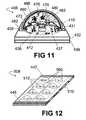
- FIG. 12shows a perspective view of another lighting component or package having light emitting chips arranged in a double-row, with a plurality of dome-shaped light-transmissive covers disposed over the light emitting chips.
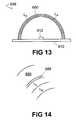
- FIG. 13shows a side sectional view of another lighting component or package having a light transmissive dome-shaped cover on which two different phosphor layers are disposed.
- FIG. 14is an enlarged sectional view of a portion of the light transmissive dome-shaped cover of FIG. 13 , showing an optional ultraviolet reflective coating is disposed between the dome-shaped cover and the phosphor layers.
- FIG. 15shows a side sectional view of another lighting component or package having a light transmissive non-dome-shaped cover on which two different phosphor layers are disposed.
- FIG. 16shows a perspective view of another lighting component or package similar to that of FIGS. 1-3 , but having the phosphor compositions screen-printed to display a corporate name and logo.
- a light emitting package 8includes a printed circuit board 10 on which one or more light emitting chips or die are disposed.
- the printed circuit boardis preferably substantially thermally conductive.
- a metal core printed circuit boardcan be employed.
- three light emitting chips or dice 12 , 14 , 16are disposed on the circuit board 10 ; however, the number of dice can be one die, two dice, or more than three dice.
- the die or dicecan be group III-nitride blue or ultraviolet light emitting diodes, red group III-phosphide or group III-arsenide light emitting diodes, II-VI light emitting diodes, IV-VI light emitting diodes, silicon or silicon-germanium light emitting diodes, or the like.
- the term “ultraviolet”is intended to encompass light emitting diode emission having a peak wavelength less than or about 425 nm.
- the die or diceare edge emitting lasers or vertical cavity surface emitting lasers.
- the light emitting chips or dicecan also be organic light emitting diodes or devices.
- Each light emitting die or dicecan be a bare die, or each die or dice can include an individual encapsulant. Still further, the die or dice can be a monolithic array of light emitting diode mesas, vertical cavity surface emitting laser mesas, or the like.
- the dice 12 , 14 , 16are disposed in corresponding reflective wells 22 , 24 , 26 ; however, the die or dice may be mounted on a planar surface of the printed circuit board 10 or can be mounted on raised pedestals or other elevated support structures. In some embodiments, a portion or all of the side of the printed circuit board 10 on which the light emitting dice or chips 12 , 14 , 16 are disposed has a reflective layer disposed thereon to improve light extraction from the package 8 .
- the illustrated printed circuit board 10includes one or more printed circuitry layers 30 sandwiched between insulative layers 32 , 34 .
- electrical padsare formed on the die attach surface of the printed circuit board 10 using appropriate vias passing through the insulative layer 32 to electrically connect the dice 12 , 14 , 16 with the printed circuitry 30 .
- the die or dice 12 , 14 , 16can be mechanically and electrically attached to the printed circuit board 10 in various ways, such as: by flip-chip bonding of die electrodes to electrical pads of the printed circuit board 10 ; by soldering the die to the board 10 and using wire bonds to electrically connect the die electrodes with electrical pads of the printed circuit board 10 ; by soldering the die to a lead frame (not shown) that is in turn mounted to the printed circuit board 10 ; or so forth.
- the die attachmentcan include a sub-mount (not shown) disposed between a light emitting die or chip and the printed circuit board or other support, or between the chip and a lead frame.
- chip bondingis achieved using thermosonic bonding, thermocompressive bonding, ultrasonic bonding, eutectic bonding with or without underfill, or so forth. Still further, rather than mounting individual dice as illustrated herein, it is contemplated to employ a monolithic light emitting diode array formed on a common substrate.
- the common substrateis soldered, thermosonically bonded, thermocompressively bonded, or otherwise secured to the printed circuit board 10 , and electrical connection to the individual light emitting mesas or structures is made by wire bonding, conductive traces formed on the common substrate, or the like.
- a monolithic array having a transparent common substratecan be configured for a flip-chip mounting in which the electrodes of the light emitting mesas or structures are directly bonded to electrical pads.
- the printed circuit board 10preferably further includes a heat sinking structure such as a ground plate or metal core 38 to provide heat sinking of the light emitting chips or dice 12 , 14 , 16 .
- a heat sinking structuresuch as a ground plate or metal core 38 to provide heat sinking of the light emitting chips or dice 12 , 14 , 16 .
- an insulative back-plate(not shown) is disposed on the side of the metal core 38 distal from the die attach surface.
- the heat sinkis optionally omitted in lower power lighting packages, packages mounted on a heat sinking surface, or the like.
- the printed circuitry layer or layers 30may provide adequate heat sinking in some embodiments.
- the material or materials forming the insulative layers 32 , 34are chosen to be thermally conductive so that these layers provide heat sinking.
- the printed circuit board 10optionally supports associated electrical components, such as a zener diode component 44 including one or more zener diodes connected across the light emitting dice 12 , 14 , 16 by the printed circuitry 30 to provide electrostatic discharge protection for the dice.
- electrical power conversion circuitry, power regulating circuitry, voltage stabilizing circuitry, current-limiting circuitry, rectifying circuitry, various combinations thereof, or the likecan be included as additional components on the printed circuit board 10 .
- Such componentscan be provided as one or more discrete components, or as an application-specific integrated circuit (ASIC).
- ASICapplication-specific integrated circuit
- an electrical plug, adaptor, electrical terminals 46 , or the likecan be disposed on the printed circuit board 10 .
- the printed circuitry 30includes traces connecting the electrical terminals 46 with the light emitting dice or chips 12 , 14 , 16 such that suitable electrical power applied to the electrical terminals 46 energizes the light emitting dice or chips 12 , 14 , 16 and associated circuitry (if any) such as the zener diode component 44 , voltage stabilizing circuitry, current limiting circuitry, or so forth.
- the printed circuit board 10can include other features such as a mounting socket, mounting openings 50 , 52 or the like for mechanically installing or securing the light emitting package 8 .
- the described printed circuit board 10is an example. Other types of printed circuit boards or other support structures can also be employed.
- the printed circuit tracescan be disposed on the die attach surface and/or on the bottom surface rather than being sandwiched between insulative layers 32 , 34 .
- the printed circuit boardcan be an electrically insulating support with a conductive trace evaporated and patterned or otherwise formed on the insulating support.
- a heat sinkcan be substituted for the printed circuit board, for example with the light emitting die or dice soldered or otherwise mechanically secured to the heat sink and with the die electrodes wire bonded to electrical pads.
- the light emitting package 8further includes a light transmissive cover 60 disposed over the light emitting dice or chips 12 , 14 , 16 .
- the light transmissive coverhas an open end defining a cover perimeter 62 that connects with the printed circuit board 10 .
- the printed circuit board 10includes an optional annular groove 66 that receives the perimeter 62 of the light transmissive cover 60 , which in the light emitting package 8 is a hemispherical dome-shaped cover.
- the groove 66guides in positioning the cover 60 on the printed circuit board 10 , and optionally also is used to help secure the cover to the board.
- the annular groove 66is omitted, in which case the placement of the cover 60 on the printed circuit board 10 is positioned by other means, such as by using an automated assembly jig.
- the light transmissive cover 60can be secured to the printed circuit board 10 in various ways, such as by an adhesive, by a friction fit between the perimeter 62 and the groove 66 , by fasteners, or so forth.
- the light transmissive cover 60 together with the printed circuit board 10define an interior volume 70 containing the light emitting dice or chips 12 , 14 , 16 .
- the connection between the perimeter 62 of the light transmissive cover 60 and the printed circuit board 10is a substantially airtight sealing connection that substantially hermetically seals the interior volume 70 .
- the connection between the perimeter 62 and the printed circuit board 10is not a hermetic seal, but rather may contain one or more gaps, openings, or the like.
- a phosphor 72(indicated by a dotted line in FIG. 3 ) is optionally disposed on an inside surface of the cover 60 . If provided, the phosphor is selected to produce a desired wavelength conversion of a portion or substantially all of the light produced by the light emitting dice or chips 12 , 14 , 16 .
- the term “phosphor”is to be understood as including a single phosphor compound or a phosphor blend or composition of two or more phosphor compounds chosen to produce a selected wavelength conversion.
- the phosphor 72may be a phosphor composition including red, green, and blue phosphor compounds that cooperatively provide white or substantially white light.
- the tri-phosphor blend of (Ba,Sr,Ca) 5 (PO 4 ) 3 Cl:Eu 2+ , Sr 4 Al 14 O 25 :Eu 2+ , and 3.5MgO*0.5MgF 2 *GeO 2 :Mn 4+ phosphorsis used.
- the phosphor compound (Ca,Sr,Ba) 2 Si 1 ⁇ c O 4 ⁇ 2c :Eu 2+ where 0 ⁇ c ⁇ 0.25is used alone or in combination with other phosphor compounds, and the phosphor is excited by a light emitting diode die or chip emitting radiation having a peak emission from about 200 nm to about 500 nm.
- the phosphor compositionincludes phosphor compounds (Ca,Sr,Ba)Al 2 O 4 :Eu 2+ , Sr 4 Al 14 O 25 :Eu 2+ , and (Ca,Sr,Ba)MgAl 10 O 17 :Eu 2+ ,Mn 2+ .
- phosphor compounds(Ca,Sr,Ba)Al 2 O 4 :Eu 2+ , Sr 4 Al 14 O 25 :Eu 2+ , and (Ca,Sr,Ba)MgAl 10 O 17 :Eu 2+ ,Mn 2+ .
- the phosphorcan include any or all of those specified ions as dopants in the formulation.
- the phosphor blendis selected to provide white light with color coordinates lying on or near the blackbody locus and a color temperature less than 4500K. In some embodiments, the phosphor blend is selected to provide white light with color coordinates lying on or near the blackbody locus and a color rendering index (R a ) of 90 or greater.
- a phosphor compositionincluding phosphor compounds Sr 4 Al 14 O 25 :Eu 2+ and (Ca,Sr,Ba)MgAl 10 O 17 :Eu 2+ ,Mn 2+ are employed to produce a green light suitable for use in application such as traffic signals.
- other listed phosphorsare also suitable for producing saturated colors and/or as phosphor compound components in white phosphor compositions.
- the light emitting dice or chips 12 , 14 , 16are blue, violet, or ultraviolet emitters such as group III-nitride light emitting diodes, and the phosphor 72 converts most or substantially all of the light generated by the chips 12 , 14 , 16 into white light.
- the light emitting dice or chips 12 , 14 , 16are blue light emitters such as group III-nitride light emitting diodes, and the phosphor 72 is a yellow phosphor that converts some of the blue light into yellow light wherein direct blue light and indirect yellow phosphor-generated light combine to produce white light.
- the light emitting dice or chips 12 , 14 , 16are blue, violet, or ultraviolet emitters and the phosphor 72 converts most or substantially all of the emitted light into light of a selected color, such as green, yellow, red, or so forth, so that the light emitting package 8 produces a colored light.
- a selected colorsuch as green, yellow, red, or so forth
- substantially any down-conversion of light produced by the light emitting dice or chips 12 , 14 , 16can be performed by suitable selection of light emitting dice or chips 12 , 14 , 16 outputting at a selected wavelength and suitable selection of the phosphor 72 .
- the phosphor 72is omitted and the direct light produced by the light emitting diodes 12 , 14 , 16 is the light output of the light emitting package.
- the light transmissive cover 60is a glass cover, where “glass” is not limited to silica-based materials but rather encompasses substantially any inorganic, amorphous light transmissive material.
- Glasstypically has better thermal stability than most plastics. Glass is more readily coated with optical coatings such as wavelength-selective reflective coatings, wavelength-selective absorbing coatings, or the like. Glass is also typically more resistant to scratching compared with most plastics.
- glasshas particular advantages in embodiments in which the light emitting dice or chips 12 , 14 , 16 produce ultraviolet or short-wavelength visible light, because light at these wavelengths can discolor or otherwise degrade the optical quality of light transmissive plastics over time.
- a glassis selected which provides high reflectivity or absorption in the ultraviolet.
- the light transmissive cover 60is made of plastic, Teflon, epoxy, EVA, acrylic, or another organic light transmissive material.
- the cover 60is made of a crystalline light transmissive material such as crystalline quartz. Such crystalline covers typically share many of the advantages of glass covers.
- the printed circuit board 10can include various reflective coatings or reflective surfaces for improving light extraction efficiency.
- substantially the entire surface of the printed circuit board on which the light emitting dice or chips 12 , 14 , 16 and the cover 60 are disposedis reflective for both light produced by the light emitting chips and for light produced by the phosphor 72 .
- that portion or area of the printed circuit board surface covered by the cover 60is reflective for both light produced by the light emitting chips and for light produced by the phosphor 72
- that portion or area of the printed circuit board surface outside of the cover 60is reflective principally for light produced by the phosphor 72 .
- each reflective coating or surfacecan be independently optimized for the spectrum of light which it is intended to reflect.
- the term “light transmissive” as used herein to describe the cover 60refers to the desired light output produced by the light emitting package 8 .
- the light outputincludes light generated by the phosphor 72 , if present, responsive to irradiation by the light emitting dice or chips 12 , 14 , 16 .
- the light outputincludes a portion or all of the direct light produced by the light emitting dice or chips 12 , 14 , 16 . Examples of the latter embodiments are a white light in which the white output light is a blending of blue light emitted by the light emitting dice or chips 12 , 14 , 16 and yellow light emitted by the phosphor 72 , or embodiments in which the phosphor 72 is omitted entirely.
- the cover 60should be at least partially light transmissive for that direct light.
- the cover 60may be light transmissive for the phosphor output but partially or wholly reflective or absorbing for the direct light produced by the light emitting dice or chips 12 , 14 , 16 .
- a light emitting packageis a white light emitting package in which the output white light is produced by the phosphor 72 responsive to ultraviolet light produced by the light emitting dice or chips 12 , 14 , 16 .
- the term “ultraviolet”is intended to encompass light produced by the light emitting dice or chips 12 , 14 , 16 whose peak wavelength is less than or about 425 nm.
- including both an ultraviolet-reflective coating on the cover 60 and an ultraviolet-reflective coating on the printed circuit board 10can effectively retain ultraviolet light produced by the ultraviolet light emitting diodes within the interior volume 70 so that the ultraviolet light has multiple opportunities through multiple reflections to interact with the phosphor 72 , thus enhancing the ultraviolet-to-white light conversion efficiency.
- the ultraviolet reflective coatingis advantageous to avoid ultraviolet absorption losses in the cover 60 .
- the ultraviolet reflecting coatingcan be disposed on the outside of the cover 60 , or as an embedded layer or thin region within the cover 60 .
- the phosphor 72can be applied to the inside surface of the light transmissive cover 60 using a suitable phosphor coating process, such as for example, electrostatic coating, slurry coating, spray coating, or so forth. Moreover, the phosphor can be disposed elsewhere besides on the inside surface of the cover 60 . For example, the phosphor can be applied to the outside surface of the cover 60 , using for example spray coating, outer surface coating, or the like, or to both the inside and outside surfaces of the cover 60 . In yet another embodiment, the phosphor is embedded in the material of the light transmissive cover 60 . However, phosphor is not readily embedded into most glass or crystalline materials. In some embodiments the phosphor is disposed in a glass binder that is spun onto or otherwise coated onto the inside and/or outside surface of the cover 60 .
- a suitable phosphor coating processsuch as for example, electrostatic coating, slurry coating, spray coating, or so forth.
- the phosphorcan be disposed elsewhere besides on the inside surface of the cover 60
- the inside surface of the cover 60is prepared by treatment with a liquid or low viscosity semi-solid material acting as a glue.
- the liquid materialcan be, for example, liquid epoxy or silicone.
- the glue materialcan be applied in a variety of ways, such as by spraying, brushing, or dipping of its working formulation or a solution thereof in a suitable solvent such as acetone, methyl isobutyl ketone (MIBK), or t-butyl acetate.
- MIBKmethyl isobutyl ketone
- the phosphoris then deposited by dusting, dipping or pouring of phosphor in powder form, the choice of deposition method being based on the nature of the inside surface of the cover 60 .
- pour phosphor powderis suitably poured into the concave inside surface of the cover 60 .
- dippingis generally a better method for coating the outside surface of the cover 60 .
- the glueis then hardened by solvent evaporation, thermal or UV curing, or the like to form the phosphor layer.
- phosphor deposition and hardening processesmay be performed, for example to deposit more than one layer of phosphor or multiple layers of phosphor blends, or as needed to attain a required thickness or layered phosphor structure.
- the phosphor coatingmay be covered with a final layer of clear glue or other suitable material to provide mechanical protection, to filter out ambient ultraviolet light or excess radiation from the light emitting dice 12 , 14 , 16 , or so forth.
- the light transmissive cover 60optionally includes one or more optical coatings besides the phosphor 72 .
- an anti-reflective coatingis applied to the inside and/or outside surface of the cover 60 to promote light transmission.
- the light transmissive cover 60optionally includes a wavelength-selective reflective coating to reflect the direct light back into the interior volume 70 where it has additional opportunity to interact with the phosphor 72 .
- the light transmissive cover 60is a single piece cover, such as a single piece glass cover, a single piece molded plastic cover, or the like. Manufacturing the cover 60 as a single piece simplifies assembly of the lighting package 8 . Another advantage of a single piece cover 60 is that a substantially hermetic sealing of the interior volume 70 is obtained by ensuring a substantially hermetic seal between the perimeter 62 of the cover 60 and the printed circuit board 10 .
- the light transmissive cover 60can include facets, fresnel lens contours, or other light refractive features that promote light scattering to produce a more spatially uniform light output.
- the light transmissive cover 60can be made of a frosted glass that has been etched with sand or the like to produce light scattering.
- the cover 60includes an anti-shatter coating such as CovRguardTM (available from General Electric Company, GE Lighting Division, Nela Park, Cleveland, Ohio), Teflon, urethane, vinyl, or so forth.
- the interior volume 70is, in the lighting package 8 , substantially filled with an encapsulant 76 .
- the encapsulant 76can be, for example, a silicone encapsulant, an epoxy encapsulant, or the like.
- the encapsulant 76is at least partially light-transmissive or substantially transparent to light produced by the light emitting dice or chips 12 , 14 , 16 and acts as a refractive index-matching material promoting light extraction out of the light emitting dice or chips 12 , 14 , 16 , and preferably also promoting light coupling with the phosphor 72 and, if the direct light produced by the light emitting dice 12 , 14 , 16 directly contributes to the package light output, also preferably promotes light transmission into the cover 60 .
- the phosphoris dispersed in a binding material that is the same material as the encapsulant 76 .
- the phosphor-binding materialis a different material that has a good refractive index match with the encapsulant 76 .
- the encapsulant 76serves as the binding material for the phosphor 72 . It will be appreciated that while the phosphor 72 is shown in FIG. 3 as residing substantially along the inside surface of the cover 60 , in some embodiments the phosphor 72 may extend some distance away from the inside surface of the cover 60 and into the encapsulant 76 disposed in the interior volume 70 .
- the phosphoris dispersed substantially into the encapsulant 76 , and may even be uniformly distributed throughout the encapsulant 76 .
- the phosphoris disposed on the inside surface of the cover 60 , or is disposed closer to the cover 60 than to the light emitting dice or chips 12 , 14 , 16 .
- light-scattering particles, particulates, or so forthare dispersed in the encapsulant 76 to provide more uniform light distribution.
- the encapsulant 76provides a common encapsulation of the light emitting dice or chips 12 , 14 , 16 which protects the chips from damage due to exposure to moisture or other detrimental environmental effects.
- the encapsulant 76may also provide potting of the light emitting dice or chips 12 , 14 , 16 to improve the robustness of the lighting package 8 and make the lighting package 8 more resistant to damage from vibrations or other mechanical disturbances.
- the cover 60is sealed to the printed circuit board 10 , and the encapsulant 76 is injected into the interior volume 70 after the light transmissive cover is sealed.
- openings 80 , 82are provided in the printed circuit board 10 .
- openingscan be provided in the light transmissive cover or at the interface between the perimeter of the cover and the printed circuit board. At least two such openings 80 , 82 are preferably provided, so that while encapsulant material is injected into one opening displaced air can exit via another opening.
- a single elongated or otherwise enlarged openingis used to provide room for both the inflowing encapsulant and the outflowing displaced air.
- the injected encapsulant 76can be a liquid or non-rigid semi-solid encapsulant, such as an optical gel, that is contained by the hermetically sealed interior volume 70 .
- the liquid or non-rigid semi-solid encapsulantmay be left uncured in some embodiments, since the hermetic seal prevents leakage of the encapsulant.
- a hermetic sealoptionally allows the encapsulant to be injected under some pressure, so that the encapsulant is at a pressure higher than atmospheric pressure.
- the interior volume 70is not hermetically sealed, and some of the injected encapsulant material may leak out.
- the light emitting dice or chips 12 , 14 , 16are mechanically and electrically connected with the printed circuit board 10 in a die attach process 102 .
- the die attachcan involve flip chip bonding, soldering, wire bonding, or so forth.
- the inside surface (and/or optionally the outside surface) of the light transmissive cover 60is coated with the phosphor 72 , if such phosphor is included in the package 8 , in a phosphorizing process 104 .
- the term “phosphorizing”denotes any method for putting a phosphor into the lighting package, such as coating or spraying a phosphor composition or compositions onto the light-transmissive cover, suspending phosphor particles in the encapsulant, embedding a phosphor in the light-transmissive cover, or so forth.
- the phosphorizing process 104is omitted and instead the phosphor is incorporated during molding or other formation of the cover 60 .
- the coveris then secured, optionally sealed, to the printed circuit board 10 in a sealing process 106 .
- the sealing process 106defines the interior volume 70 , which is optionally a hermetically sealed volume.
- the encapsulant 76is then injected into the interior volume 70 through the openings 80 , 82 in an encapsulant injection process 108 .
- the encapsulantis cured in a curing process 110 if the encapsulant material requires curing.
- the openings 80 , 82are optionally sealed with a suitable sealing material in a sealing process 112 .
- the encapsulant 76also seals the openings 80 , 82 , and so in these embodiments the separate sealing process 112 is omitted.
- another lighting package 8 ′includes a printed circuit board 10 ′ and a light transmissive cover 60 ′ having an open end defining a cover perimeter 62 ′, which are illustrated in FIG. 5 and correspond to the printed circuit board 10 , cover 60 , and cover perimeter 62 ′, respectively, of the lighting package 8 .
- the lighting package 8 ′also includes most other components of the lighting package 8 which however are not visible in the outside perspective view of FIG. 5 .
- the lighting package 8 ′differs from the lighting package 8 of FIGS. 1-3 in that the electrical terminals 46 of the lighting package 8 are replaced in the lighting package 8 ′ by four electrical terminals 46 ′ disposed on the backside of the printed circuit board 10 ′.
- the electrical terminals 46 ′are electrically connected with the light emitting die or dice disposed in the cover 60 ′ by suitable printed circuitry residing in or on the printed circuit board 10 ′.
- the backside electrical terminals 46 ′can be configured, for example, to insert into matching openings of a four-prong surface-mount receptacle socket.
- the phosphor composition 72includes a mixture of at least two constituent phosphor compositions each possessing essentially the same emission color coordinates (for example x and y coordinates on the 1931 CIE chromaticity diagram) but different color rendering index (CRI) values.
- the at least two different constituent phosphor compositionsare different in that they differ by at least one phosphor compound.
- the first constituent phosphor compositionmay include blue, green, and yellow phosphor compounds A, B, and C, respectively, with a stoichiometry producing white or substantially white light at a first CRI value;
- the second constituent phosphor compositionmay include green, yellow, and red phosphor compounds B, C, and D, respectively, with a stoichiometry producing white or substantially white light at a second, different CRI value.
- the blue, green, yellow, and red phosphor compounds A, B, C, and Dare respectively (Ba,Sr,Ca) 5 (PO 4 ) 3 Cl:Eu 2+ , Sr 4 Al 14 O 25 :Eu 2+ , (Ca,Sr,Ba) 2 Si 1 ⁇ c O 4 ⁇ 2c :Eu 2+ where 0 ⁇ c ⁇ 0.25, and 3.5MgO*0.5MgF 2 *GeO 2 :Mn 4+ .
- the output converted light consisting of a blending of the constituent converted light of the first and second phosphor compositionshas a CRI value that is different from, and possibly larger than, the first or second CRI value of the individual constituent phosphor compositions.
- the first phosphor composition (A,B,C)can have stoichiometries whose color coordinates span a triangle having as vertices the color points of the phosphor compounds A, B, and C.
- the second phosphor composition (B,C,D)can have stoichiometries whose color coordinates span a triangle having as vertices the color points of the phosphor compounds B, C, and D.
- a cross-hatched triangle having as vertices the color points of the common phosphor compounds B and C and a third vertex Edenote the range of color coordinates that can be achieved using suitable stoichiometries of either phosphor composition (A,B,C) or phosphor composition (B,C,D).
- CRI tuning and/or luminosity tuningis achievable by blending or combining the first and second phosphor compositions with stoichiometries corresponding to about the same color point. This approach enables CRI tuning by selecting the ratio of the first (A,B,C) constituent phosphor composition and second (B,C,D) constituent phosphor composition.
- each constituent phosphor compositionproducing constituent converted light at substantially the same color point responsive to irradiation by emission of the light emitting die or chip 612 (preferably but not necessarily in the ultraviolet range, such as peak chip emission wavelength less than or about 425 nm).
- the number of phosphor compounds per constituent phosphor compositioncan be anywhere from one (such as, for example, suitable phosphor compounds disclosed in U.S. Pat. No. 6,522,065) to two, three or more (such as, for example, suitable phosphor blends disclosed in U.S. Pat. No. 6,685,852).
- the at least two different constituent phosphor compositionsshould preferably provide substantially the same color point when excited by emission of the light emitting die or chip 612 , preferably to within about 0.020 units in both x and y color coordinates on the 1931 CIE chromaticity diagram, more preferably to within 0.010 units, and still more preferably to within 0.005 units.
- the amount of the two constituent phosphor compositions relative to each otheris selected to optimize the light output respective to color rendering index (CRI) at a given minimal luminosity threshold, or vice versa, at a selected color point.
- CRIcolor rendering index
- the ratio or blending of two or more constituent phosphor compositions of substantially the same color point but different CRI valuesBy varying the ratio or blending of two or more constituent phosphor compositions of substantially the same color point but different CRI values, one can alter the final CRI and luminosity characteristics of the device in a continuous fashion.
- a mixture of the constituent phosphor compositionsBy using a mixture of the constituent phosphor compositions, a continuous range of CRI values are achievable.
- the CRI value of the blended lightmay be larger than the CRI value of any of the constituent phosphor compositions acting alone.
- the CRIe.g. maximize it for a given minimal luminosity requirement
- the luminositye.g.
- the lighting device 608is tunable without affecting the chemical makeup of either the phosphor compounds or the constituent phosphor compositions configured for the color point target.
- Some suitable approaches for optimizing or selecting the CRI using two or more constituent phosphor compositions having about the same color coordinatesare disclosed in co-pending application Ser. No. 10/909,564 filed Nov. 2, 2004 which is incorporated by reference herein in its entirety.
- the at least two different constituent phosphor compositionsare selected to provide white light with color coordinates lying on or near the blackbody locus and a color temperature less than 4500K.
- the at least two different constituent phosphor compositionsare selected to blend to produce white light with a color rendering index (R a ) of 90 or greater.
- Example FIG. 7shows a CRI-tuned converted light spectrum using a mixture of the aforementioned (A,B,C) and (B,C,D) phosphor compositions that provided a correlated color temperature of about 3300K and a CRI value of about 90.
- the color temperaturewas about 3500K and the CRI value was about 91.
- Higher or lower CRI valuesare attainable at the same color point or another color point attainable by both phosphor compositions by varying the ratio of the phosphor compositions, by using a technique such as Design of Experiment (DOE).
- DOEDesign of Experiment
- the CRI-tuning mixture of phosphor compositions (A,B,C) and (B,C,D)is an example.
- Other mixturescan be used so long as the constituent phosphor compositions produce converted light at about the same color point of interest.
- the constituent phosphor compositionseach produce constituent converted light which is white light or substantially white light, that is, which lies on or substantially on the black body locus of the 1931 CIE chromaticity diagram.
- Such constituent phosphor compositionsare suitably operated in conjunction with one or more ultraviolet light emitting chips or dice, that is, with chips or dice that emit peak radiation below or about at 425 nm.
- the bleed-through light produced by the at least one light emitting diehas a negligible contribution to the visible spectrum of the converted light of the different phosphor compositions blended with bleed-through light produced by the at least one light emitting die.
- This negligible contributioncan result from an arrangement in which the conversion efficiency of the light produced by the at least one light emitting die is close to 100%.
- This negligible contributioncan also result from the at least one light emitting die emitting light substantially outside of the visible spectrum.
- the output converted light produced by blending of the constituent converted light of the constituent phosphor compositions combined with radiation produced by the at least one light emitting die that bleeds through the phosphor layer 72 to contribute to light output of the light emitting package 8is white light or substantially white light, that is, lies on or substantially on the black body locus of the 1931 CIE chromaticity diagram.
- the phosphor compositionshave color points corresponding to yellowish or orangish light and are suitably operated in conjunction with one or more blue light emitting chips or dice, that is, with chips or dice that emit peak radiation in the blue or bluish visible range.
- the bleed-through blue or bluish lightcombines with the yellowish or orangish converted light to provide white light output of the light emitting package.
- the phosphor compositionsproduce white or substantially white light with low intensity in the blue or bluish range, and the one or more light emitting chips or dice emit peak radiation in the blue or bluish visible range that bolsters the spectrum of the blended light in the blue or bluish range of the visible spectrum.
- another lighting package 8 ′′includes a printed circuit board 10 ′′, having a long strip shape, on which a plurality of light emitting dice or chips 12 ′′ are arranged in reflective wells 22 ′′ in a double-row arrangement along the board strip.
- the printed circuit board 10 ′′includes one or more printed circuitry layers 30 ′′ sandwiched between insulative layers 32 ′′, 34 ′′, and a ground plate or metal core 38 ′′. Electrical terminals 46 ′′ disposed on the printed circuit board 10 ′′ deliver electrical power to the light emitting dice or chips 12 ′′ via the printed circuitry 30 ′′.
- a light transmissive cover 60 ′′is tube-shaped to cover the long double-row of light emitting dice or chips 12 ′′ and has an open end defining a perimeter 62 ′′ that is received by a matching groove 66 ′′ formed in the printed circuit board 10 ′′.
- the tube-shaped cover 60 ′′ together secured to the printed circuit board 10 ′′define an elongated or tubular interior volume 70 ′′ containing the light emitting dice or chips 12 ′′.
- a phosphor 72 ′′optionally coats an inside surface of the tube-shaped cover 60 ′′.
- An encapsulant 76 ′′substantially fills the interior volume 70 ′′ to encapsulate and pot the light emitting dice or chips 12 ′′ and the optional phosphor 72 ′′.
- yet another lighting package 208includes a printed circuit board 210 on which one or more (specifically three in the illustrated embodiment) light emitting dice or chips 212 are arranged.
- the light emitting dice or chips 212are not disposed in reflective wells; rather, they are surface-mounted to a level surface of the printed circuit board 210 .
- the printed circuit board 210includes one or more printed circuitry layers 230 sandwiched between insulative layers 232 , 234 , and a ground plate or metal core 238 .
- a zener diode component 244provides electrostatic discharge protection for the light emitting dice or chips 212 .
- a light transmissive cover 260covers the light emitting dice or chips 212 and has an open end defining a perimeter 262 that is connected with the printed circuit board 210 to define an interior volume 270 containing the light emitting dice or chips 212 .
- a phosphor 272optionally coats an inside surface of the light transmissive cover 260 .
- the lighting package 208differs from the lighting package 8 in the configuration of the encapsulant disposed in the interior volume.
- a first encapsulant 276encapsulates and optionally pots the light emitting dice or chips 212 , but does not substantially fill the interior volume 270 .
- the first encapsulant 276may encapsulate only the one or more light emitting dice 212 .
- a second encapsulant 278encapsulates the phosphor 272 if such a phosphor is included in the package 208 .
- the second encapsulant 278is the binding material of the phosphor 270 .
- the phosphor 272may be applied to the inside surface of the cover 260 , and the encapsulant in this embodiment is the binding material of the applied phosphor.
- the first and second encapsulants 276 , 278can be different materials.
- a substantial gap 280extends between the first and second encapsulants 276 , 278 .
- the gap 280contains air; however, it is also contemplated to fill the gap 280 with an inert gas to reduce moisture in the lighting package 208 .
- the gap 280is filled with a third encapsulant different from at least one of the first and second encapsulants 276 , 278 .
- the lighting package 208there is no groove in the printed circuit board 210 for receiving the perimeter 262 of the cover 260 .
- a groove similar to the groove 66 of the lighting package 8can optionally be provided to align and optionally help secure the cover 260 to the printed circuit board 210 .
- the light emitting dice or chips 212are mechanically and electrically connected with the printed circuit board 210 in a die attach process 302 .
- the die attachcan involve flip chip bonding, soldering, wire bonding, or so forth.
- the attached light emitting dice 212are encapsulated or potted on the printed circuit board 210 in a first encapsulation process 304 , and the first encapsulant 276 is cured in a first curing process 306 applied to the printed circuit board 210 .
- the inside surface (and/or optionally the outside surface) of the light transmissive cover 260is coated with the phosphor 272 in a phosphorizing process 310 .
- the phosphorizing process 310is omitted and instead the phosphor is incorporated during molding or other formation of the cover 260 .
- the phosphoris encapsulated on the light transmissive cover 260 in a second encapsulation process 312 , and the second encapsulant 278 is cured in a second curing process 314 applied to the light transmissive cover 314 .
- the phosphor 272is omitted from the package 208 , then process 310 , 312 , and 314 are suitably omitted.
- the second encapsulant 278is the binding material of the phosphor 272 ; in these embodiments, the phosphorization process 310 and the second encapsulation process 312 are integrated.
- the light transmissive coveris then secured, optionally sealed, to the printed circuit board 210 in a securing process 316 .
- the securing process 316defines the interior volume 270 , which is optionally a hermetically sealed volume.
- still yet another lighting package 408includes a printed circuit board 410 on which a single light emitting die or chip 412 is surface-mounted to a level surface of the printed circuit board 410 .
- the printed circuit board 410includes two printed circuit traces 430 , 431 disposed on the same surface as the light emitting die 412 .
- the two conductive traces 430 , 431can be formed by metal evaporation or the like.
- Wire bonds 436 , 437connect top-side electrodes of the light emitting die or chip 412 with the conductive traces 430 , 431 .
- the printed circuit boardincludes an insulative layer 432 on which the two printed circuit traces 430 , 431 are formed, and an optional ground plate or metal core 438 .
- a light transmissive cover 460covers the light emitting die or chip 412 and has an open end defining a perimeter 462 that is connected with the printed circuit board 410 to define an interior volume 470 containing the light emitting die or chip 412 .
- the two printed circuit traces 430 , 431extend from inside the cover 460 to outside the cover 460 to provide electrical communication into the interior volume 470 .
- a phosphor 472optionally coats an inside surface of the light transmissive cover 460 , and an encapsulant 476 substantially fills the interior volume 470 .
- Hemispherical openings 480 , 482 formed at the perimeter 462 of the light transmissive cover 460allow for injection of the encapsulant material and corresponding displacement of air. That is, the openings 480 , 482 of the lighting package 408 serve the same purpose as the printed circuit board openings 80 , 82 of the lighting package 8 (see FIG. 3 ).
- a reflective coating 488coats the inside surface of the light transmissive cover.
- the reflective coating 488is substantially reflective for light produced by the light emitting die or chip 412 but is substantially transmissive for light produced by the phosphor 472 responsive to illumination by the light emitting die or chip 412 .
- the phosphor 472is disposed on the reflective coating 488 and extends some distance into the encapsulant 476 .
- a common printed circuit board 510supports a plurality of light transmissive dome-shaped covers 560 each covering one or more light emitting dice 512 .
- Printed circuitry of the common printed circuit board 510connects the light emitting dice 512 with edge terminals 446 , 447 that are adapted for connection with a DIN-type rail lighting fixture.
- edge terminals 446 , 447that are adapted for connection with a DIN-type rail lighting fixture.
- other types of terminalsare employed.
- the electric terminals 46 shown in FIG. 1can be used.
- the printed circuit board 510is a flexible printed circuit board, so that the light source of FIG. 12 is a flexible sheet lighting source.
- the light emitting covers 560provide mechanical protection for the light emitting dice 512 .
- the perimeter of each light transmissive dome-shaped cover 560is secured to the flexible printed circuit board in a manner so as to impart tensile strain to the portion of the flexible circuit board covered by the dome-shaped cover 560 .
- the portions of the flexible printed circuit board on which the light emitting dice 512 are disposedare kept substantially rigid by the tensile strain as the flexible printed circuit board is flexed, thus reducing a likelihood that the flexing will break the connections or bonds of the light emitting dice 512 with the printed circuit board.
- the light transmissive dome-shaped covers 560are arranged close together such that, together with light-dispersive properties of the covers 560 , optional dispersive particles disposed in an encapsulant within the covers 560 , light spreading provided by the distribution of phosphor across the covers 560 , or so forth, a spatially uniform planar lighting source 508 is formed that produces little or no perceptible pixilation of the illumination at typical illumination source-to-target distances.
- One advantage of the lighting packaging techniques disclosed hereinis flexibility in deployment of phosphor compositions.
- One or more phosphor layersare readily disposed on the inner surface of the cover, for example as described previously with respect to phosphorization operations 104 , 310 of FIGS. 4 and 10 , respectively.
- Application of a layer of phosphor to a glass or plastic cover surfacecan be done in a precise and readily controllable manner.
- Each phosphor layersuitably includes a phosphor composition comprising one or more phosphor compounds.
- a lighting package 608includes a printed circuit board 610 supporting a light emitting die or chip 612 , or optionally more than one light emitting die or chip, covered by a light transmissive cover 660 .
- the lighting package 608is similar to the lighting package 8 of FIGS. 1-3 .
- the lighting package 608includes two phosphor layers L A , L B of different phosphor compositions disposed on an inner surface of the light-transmissive dome-shaped cover 660 .
- the phosphor composition of phosphor layer L Bis different from the phosphor composition of layer L A in that they include at least one different phosphor compound.
- the lighting package 608optionally includes other features set forth herein with respect to other embodiments, such as an optional ultraviolet reflective coating 688 diagrammatically shown in FIG. 14 disposed between the cover 660 and the phosphor layers L A , L B .
- the ultraviolet reflective coating 688is useful for embodiments in which the light emitting die or chip 612 emits ultraviolet light while the phosphor layers L A , L B generate visible light.
- the dome-shaped cover 660provides a convenient platform for arranging one, two, or more phosphor layers each of which emits a spatially uniform distribution of light subtending about 2 ⁇ steradians or more.
- the first phosphor layer L Amay include a first constituent phosphor composition of blue, green, and yellow phosphor compounds A, B, and C, respectively, with a stoichiometry producing white or substantially white light at a first CRI value
- the second phosphor layer L Bmay include a second constituent phosphor composition of green, yellow, and red phosphor compounds B, C, and D, respectively, with a stoichiometry producing white or substantially white light at a second, different CRI value.
- the layered combination of the first constituent phosphor composition of layer L A and the second constituent phosphor composition of layer L Bproduces a CRI value that is different from, and possibly larger than, the first or second CRI value.
- CRI tuning using a single layer containing two or more constituent phosphor compositions of about the same color pointhas been described with example reference to FIG. 3 .
- CRI tuning using a layered structure in which each layer contains one of the constituent phosphor compositions of about the same color pointhas been described with example reference to FIGS. 13 and 14 .
- the two or more constituent phosphor compositions whose light is blended to produce a tailored CRI and/or luminositycan be combined in other physical arrangements, such as being disposed as distinct patterns in a single layer.
- one of the phosphor compositionsmay become saturated at high levels of irradiation intensity by the light emitting die or chip 612 .
- the layered arrangement of FIGS. 13 and 14can also be useful in addressing such saturation issues.
- the more easily saturated phosphor compositionis suitably arranged as the phosphor layer L A that is furthest from the light emitting die or chip 612 , since partial absorption of light by the intervening phosphor composition of phosphor layer L B can be expected to reduce the excitation light flux of the phosphor composition in layer L A , thus facilitating more efficient light conversion.
- the phosphorscan be disposed in other spatially separated arrangements besides layers.
- the first phosphor compositionmay be arranged physically as a layer disposed on an inside or outside surface of the light-transmissive cover, while the second phosphor composition may be dispersed in an encapsulant filling the interior volume.
- FIG. 15shows a lighting package 708 that includes a printed circuit board 710 supporting a light emitting die or chip 712 , or optionally more than one light emitting die or chip, covered by a light transmissive cover 760 .
- the lighting package 708is similar to the lighting package 608 of FIGS. 13 and 14 , except that the light-transmissive cover 760 has a different geometry than the dome-shaped cover 660 of FIGS. 13 and 14 .
- the light-transmissive cover 760includes a reflective side portion or portions 760 R that channel light (indicated diagrammatically in FIG.
- the two phosphor layers L X , L Y of different phosphor compositionsare disposed on the light-transmissive top portion 760 T .
- the two phosphor layers L X , L Ymay also extend along the inside of the reflective side portion 760 R of the light-transmissive cover 760 .
- the phosphor layersare disposed only on the inside reflective side portion 760 R of the light-transmissive cover 760 , while the light-transmissive top portion 760 T is left uncoated by phosphor.
- the light-transmissive top portion 760 Tis preferably absorbing or reflective for ultraviolet light to prevent direct ultraviolet light from being emitted from the lighting package 708 .
- FIG. 16shows a perspective view of another lighting component or package similar to that of FIGS. 1-3 , but having two different phosphor compositions disposed on different regions 800 , 802 screen-printed on the light-transmissive dome-shaped cover 60 .
- the screen-printed phosphor region 800spells out “Acme Corp.” along with a corresponding logo, while the screen-printed phosphor region 802 covers the area of the light-transmissive dome-shaped cover 60 not covered by the phosphor regions 800 .
- the phosphor composition of the region 800emits red light while the phosphor composition of the region 802 emits white light
- the name “Acme Corp.” and corresponding logoappears in as a red light-emissive text and symbol on a white light emissive background.
- both the foreground (e.g., text or logo artwork) and the backgroundare light-emissive.
Landscapes
- Engineering & Computer Science (AREA)
- Power Engineering (AREA)
- Microelectronics & Electronic Packaging (AREA)
- Physics & Mathematics (AREA)
- Condensed Matter Physics & Semiconductors (AREA)
- General Physics & Mathematics (AREA)
- Computer Hardware Design (AREA)
- Led Device Packages (AREA)
Abstract
Description
- (Mg,Ca,Sr,Ba,Zn)5(PO4)3Cl:Eu2+
- (Ca,Sr,Ba)2Si1−cO4−2c:Eu2+ where 0≦c<0.25
- (Ba,Sr,Ca)5(PO4)3(Cl,F,Br,OH):Sb3+,Mn2+
- (Mg,Ca,Sr,Ba,Zn)5(PO4)3(F,Cl,Br,OH):Eu2+,Mn2+
- (Ba,Sr,Ca)BPO5:Eu2+,Mn2+
- (Sr,Ca)10(PO4)6*nB2O3:Eu2+
- Sr2Si3O8*2SrCl2:Eu2+
- Sr4Al14O25:Eu2+
- (Ca,Sr,Ba)MgAl10O17:Eu2+,Mn2+
- Ba3MgSi2O8:Eu2+
- BaAl8O13:Eu2+
- 2SrO*0.84P2O5*0.16B2O3:Eu2+;
- (Ba,Sr,Ca)Al2O4:Eu2+
- (Y,Gd,Lu,Sc,La)BO3:Ce3+,Tb3+
- Ca8Mg(SiO4)4Cl2:Eu2+,Mn2+
- (Ba,Sr,Ca)2(Mg,Zn)Si2O7:Eu2+
- (Sr,Ca,Ba)(Al,Ga,In)2S4:Eu2+
- (Y,Gd,Tb,La,Sm,Pr,Lu)3(Al,Ga)5−fO12−3/2f:Ce3+ (wherein 0≦f≦0.5)
- (Lu,Y,Sc)2−g(Ca,Mg)1+gLihMg2−h(Si,Ge)3−hPhO12−g:Ce3+ (wherein 0≦g≦0.5, 0≦h≦0.5)
- (Ca,Sr)8(Mg,Zn)(SiO4)4Cl2:Eu2+,Mn2+
- Na2Gd2B2O7:Ce3+, Tb3+
- (Sr,Ca,Ba,Mg,Zn)2P2O7:Eu2+,Mn2+
- (Ca,Sr,Ba,Mg, Zn)10(PO4)6(F,Cl,Br,OH)2:Eu2+,Mn2+
- (Gd,Y,Lu,La)2O3:Eu3+,Bi3+
- (Gd,Y,Lu,La)2O2S:Eu3+,Bi3+
- (Gd,Y,Lu,La)VO4:Eu3+,Bi3+
- SrY2S4:Eu2+
- CaLa2S4:Ce3+
- (Ca,Sr)S:Eu2+
- (Ba,Sr,Ca)MgP2O7:Eu2+,Mn2+
- (Y,Lu)2WO6:Eu3+,Mo6+
- (Ba,Sr,Ca)uSiv(N,O)w:Eu2+
- (Lu,Ca,Li,Mg,Y)alpha-SiAlON doped with Eu2+ and/or Ce3+
- (Y,Lu,Gd)2−tCatSi4N6+tC1−t:Ce3+ (wherein 0≦t≦0.5)
- 3.5MgO*0.5MgF2*GeO2:Mn4+
- A2[MF6]:Mn4+, where A=Li, Na, K, Rb or Cs and M=Ge, Si, Sn, Ti or Zr
- Ca1−d−eCedEueAl1−d(Mg,Zn)dSiN3.
Those skilled in the art can readily select other phosphor compounds suitable for performing specific light conversions.
Claims (29)
Priority Applications (6)
| Application Number | Priority Date | Filing Date | Title |
|---|---|---|---|
| US11/312,268US7800121B2 (en) | 2002-08-30 | 2005-12-20 | Light emitting diode component |
| PCT/US2006/047869WO2007075393A1 (en) | 2005-12-20 | 2006-12-15 | Light package |
| US12/884,612US8362695B2 (en) | 2002-08-30 | 2010-09-17 | Light emitting diode component |
| US12/884,717US8436380B2 (en) | 2002-08-30 | 2010-09-17 | Light emitting diode component |
| US13/886,878US10309587B2 (en) | 2002-08-30 | 2013-05-03 | Light emitting diode component |
| US14/062,169US10340424B2 (en) | 2002-08-30 | 2013-10-24 | Light emitting diode component |
Applications Claiming Priority (5)
| Application Number | Priority Date | Filing Date | Title |
|---|---|---|---|
| US40742602P | 2002-08-30 | 2002-08-30 | |
| PCT/US2003/027363WO2004021461A2 (en) | 2002-08-30 | 2003-08-29 | Phosphor-coated led with improved efficiency |
| US10/831,862US7224000B2 (en) | 2002-08-30 | 2004-04-26 | Light emitting diode component |
| US10/909,564US7768189B2 (en) | 2004-08-02 | 2004-08-02 | White LEDs with tunable CRI |
| US11/312,268US7800121B2 (en) | 2002-08-30 | 2005-12-20 | Light emitting diode component |
Related Parent Applications (4)
| Application Number | Title | Priority Date | Filing Date |
|---|---|---|---|
| PCT/US2003/027363Continuation-In-PartWO2004021461A2 (en) | 2002-08-30 | 2003-08-29 | Phosphor-coated led with improved efficiency |
| US10831862Continuation-In-Part | 2003-08-29 | ||
| US10/831,862Continuation-In-PartUS7224000B2 (en) | 2002-08-30 | 2004-04-26 | Light emitting diode component |
| US10/909,564Continuation-In-PartUS7768189B2 (en) | 2002-08-30 | 2004-08-02 | White LEDs with tunable CRI |
Related Child Applications (3)
| Application Number | Title | Priority Date | Filing Date |
|---|---|---|---|
| US10/909,564ContinuationUS7768189B2 (en) | 2002-08-30 | 2004-08-02 | White LEDs with tunable CRI |
| US12/884,612ContinuationUS8362695B2 (en) | 2002-08-30 | 2010-09-17 | Light emitting diode component |
| US12/884,717ContinuationUS8436380B2 (en) | 2002-08-30 | 2010-09-17 | Light emitting diode component |
Publications (2)
| Publication Number | Publication Date |
|---|---|
| US20060097245A1 US20060097245A1 (en) | 2006-05-11 |
| US7800121B2true US7800121B2 (en) | 2010-09-21 |
Family
ID=37909703
Family Applications (3)
| Application Number | Title | Priority Date | Filing Date |
|---|---|---|---|
| US11/312,268Expired - LifetimeUS7800121B2 (en) | 2002-08-30 | 2005-12-20 | Light emitting diode component |
| US12/884,717Expired - Fee RelatedUS8436380B2 (en) | 2002-08-30 | 2010-09-17 | Light emitting diode component |
| US12/884,612Expired - LifetimeUS8362695B2 (en) | 2002-08-30 | 2010-09-17 | Light emitting diode component |
Family Applications After (2)
| Application Number | Title | Priority Date | Filing Date |
|---|---|---|---|
| US12/884,717Expired - Fee RelatedUS8436380B2 (en) | 2002-08-30 | 2010-09-17 | Light emitting diode component |
| US12/884,612Expired - LifetimeUS8362695B2 (en) | 2002-08-30 | 2010-09-17 | Light emitting diode component |
Country Status (2)
| Country | Link |
|---|---|
| US (3) | US7800121B2 (en) |
| WO (1) | WO2007075393A1 (en) |
Cited By (22)
| Publication number | Priority date | Publication date | Assignee | Title |
|---|---|---|---|---|
| US20070168000A1 (en)* | 2006-01-13 | 2007-07-19 | Happawana Gemunu S | Apparatus and method for cooling lasers using insulator fluid |
| US20100123151A1 (en)* | 2008-11-20 | 2010-05-20 | Toshio Hata | Light-emitting device |
| US20100207134A1 (en)* | 2007-07-26 | 2010-08-19 | Kenichiro Tanaka | Led lighting device |
| US20100213808A1 (en)* | 2009-02-26 | 2010-08-26 | Wei Shi | Heat sink base for LEDS |
| US20100237375A1 (en)* | 2007-12-07 | 2010-09-23 | Panasonic Electric Works Co., Ltd. | Light Emitting Device |
| US20110272713A1 (en)* | 2008-11-13 | 2011-11-10 | Osram Opto Semiconductors Gmbh | Optoelectronic component |
| US20120236573A1 (en)* | 2009-12-07 | 2012-09-20 | Shoji Yamamoto | Lighting apparatus |
| US20130194792A1 (en)* | 2005-12-21 | 2013-08-01 | Cree, Inc. | Lighting device and lighting method |
| US20130320390A1 (en)* | 2011-02-18 | 2013-12-05 | 3M Innovative Properties Company | Flexible light emitting semiconductor device |
| US20140204572A1 (en)* | 2013-01-21 | 2014-07-24 | Thomas Spinelli | System for Adapting an Existing Florescent Light Fixture with an LED Luminaire |
| US20150116999A1 (en)* | 2013-10-30 | 2015-04-30 | Avago Technologies General Ip (Singapore) Pte. Ltd | Mono-axial lens for multiple light sources |
| US9236547B2 (en) | 2011-08-17 | 2016-01-12 | 3M Innovative Properties Company | Two part flexible light emitting semiconductor device |
| US20160025277A1 (en)* | 2013-01-21 | 2016-01-28 | Thomas Spinelli | System for adapting an existing fluorescent light fixture with an LED luminaire |
| US9564568B2 (en) | 2010-11-03 | 2017-02-07 | 3M Innovative Properties Company | Flexible LED device with wire bond free die |
| US9674938B2 (en) | 2010-11-03 | 2017-06-06 | 3M Innovative Properties Company | Flexible LED device for thermal management |
| US9698563B2 (en) | 2010-11-03 | 2017-07-04 | 3M Innovative Properties Company | Flexible LED device and method of making |
| US9871173B2 (en) | 2015-06-18 | 2018-01-16 | Cree, Inc. | Light emitting devices having closely-spaced broad-spectrum and narrow-spectrum luminescent materials and related methods |
| US10340424B2 (en) | 2002-08-30 | 2019-07-02 | GE Lighting Solutions, LLC | Light emitting diode component |
| WO2019246426A1 (en)* | 2018-06-20 | 2019-12-26 | Veeco Precision Surface Processing Llc | An apparatus and method for the minimization of undercut during a ubm etch process |
| US10541353B2 (en) | 2017-11-10 | 2020-01-21 | Cree, Inc. | Light emitting devices including narrowband converters for outdoor lighting applications |
| US10891881B2 (en) | 2012-07-30 | 2021-01-12 | Ultravision Technologies, Llc | Lighting assembly with LEDs and optical elements |
| US11069583B2 (en) | 2018-06-20 | 2021-07-20 | Veeco Instruments Inc. | Apparatus and method for the minimization of undercut during a UBM etch process |
Families Citing this family (163)
| Publication number | Priority date | Publication date | Assignee | Title |
|---|---|---|---|---|
| US7368179B2 (en) | 2003-04-21 | 2008-05-06 | Sarnoff Corporation | Methods and devices using high efficiency alkaline earth metal thiogallate-based phosphors |
| AT501081B8 (en)* | 2003-07-11 | 2007-02-15 | Tridonic Optoelectronics Gmbh | LED AS WELL AS LED LIGHT SOURCE |
| JP3837588B2 (en) | 2003-11-26 | 2006-10-25 | 独立行政法人物質・材料研究機構 | Phosphors and light emitting devices using phosphors |
| US10499465B2 (en) | 2004-02-25 | 2019-12-03 | Lynk Labs, Inc. | High frequency multi-voltage and multi-brightness LED lighting devices and systems and methods of using same |
| US10575376B2 (en) | 2004-02-25 | 2020-02-25 | Lynk Labs, Inc. | AC light emitting diode and AC LED drive methods and apparatus |
| WO2011143510A1 (en) | 2010-05-12 | 2011-11-17 | Lynk Labs, Inc. | Led lighting system |
| US11355676B2 (en) | 2004-05-07 | 2022-06-07 | Bruce H. Baretz | Light emitting diode |
| EP1769050B1 (en) | 2004-07-06 | 2013-01-16 | Lightscape Materials Inc. | Efficient, green-emitting phosphors, and combinations with red-emitting phosphors |
| US7315048B2 (en)* | 2004-10-22 | 2008-01-01 | Avago Technologies Ecbu Ip (Singapore) Pte Ltd | Method and apparatus for mixing light emitted by a plurality of solid-state light emitters |
| WO2006098450A1 (en) | 2005-03-18 | 2006-09-21 | Mitsubishi Chemical Corporation | Light-emitting device, white light-emitting device, illuminator, and image display |
| US7276183B2 (en)* | 2005-03-25 | 2007-10-02 | Sarnoff Corporation | Metal silicate-silica-based polymorphous phosphors and lighting devices |
| EP1887067B1 (en) | 2005-05-24 | 2014-04-16 | Mitsubishi Chemical Corporation | Phosphor and use thereof |
| US9412926B2 (en) | 2005-06-10 | 2016-08-09 | Cree, Inc. | High power solid-state lamp |
| ITMI20051874A1 (en)* | 2005-10-05 | 2007-04-06 | Terza Luce S R L | HIGH-INTEGRATION POWER LED LAMP |
| US20070125984A1 (en)* | 2005-12-01 | 2007-06-07 | Sarnoff Corporation | Phosphors protected against moisture and LED lighting devices |
| US8906262B2 (en)* | 2005-12-02 | 2014-12-09 | Lightscape Materials, Inc. | Metal silicate halide phosphors and LED lighting devices using the same |
| WO2007097110A1 (en)* | 2006-02-24 | 2007-08-30 | Nec Corporation | Optical communication system, and optical transmitter |
| US8998444B2 (en)* | 2006-04-18 | 2015-04-07 | Cree, Inc. | Solid state lighting devices including light mixtures |
| WO2007139781A2 (en)* | 2006-05-23 | 2007-12-06 | Cree Led Lighting Solutions, Inc. | Lighting device |
| US7661840B1 (en) | 2006-06-21 | 2010-02-16 | Ilight Technologies, Inc. | Lighting device with illuminated front panel |
| BRPI0714428A2 (en)* | 2006-07-13 | 2013-03-12 | Tir Technology Lp | SOURCE OF LIGHT, METHOD FOR DRIVING THE SAME, COMPUTER PROGRAM PRODUCT, AND COMPUTER-READY STORAGE MEDIA |
| US7804147B2 (en)* | 2006-07-31 | 2010-09-28 | Cree, Inc. | Light emitting diode package element with internal meniscus for bubble free lens placement |
| US20080029720A1 (en)* | 2006-08-03 | 2008-02-07 | Intematix Corporation | LED lighting arrangement including light emitting phosphor |
| US7842960B2 (en)* | 2006-09-06 | 2010-11-30 | Lumination Llc | Light emitting packages and methods of making same |
| KR20090057114A (en)* | 2006-09-27 | 2009-06-03 | 가부시끼가이샤 도시바 | Semiconductor light emitting device, backlight and display device comprising the semiconductor light emitting device |
| CN101605867B (en) | 2006-10-03 | 2013-05-08 | 渲染材料公司 | Metal silicate halide phosphors and LED lighting devices using them |
| KR101370372B1 (en)* | 2006-10-18 | 2014-03-05 | 코닌클리케 필립스 엔.브이. | Illumination system and display device |
| JP2008108861A (en)* | 2006-10-25 | 2008-05-08 | Avago Technologies Ecbu Ip (Singapore) Pte Ltd | Light emitting diode package with flexible PCB directly connected to light source |
| US20080145622A1 (en)* | 2006-12-14 | 2008-06-19 | Roy Mihir K | Polymer-based integrated thin film capacitors, packages containing same and methods related thereto |
| DE112007002696T5 (en) | 2006-12-26 | 2009-11-05 | Seoul Opto Device Co. Ltd., Ansan | Light emitting device |
| JP2008166782A (en)* | 2006-12-26 | 2008-07-17 | Seoul Semiconductor Co Ltd | Light emitting element |
| US7686478B1 (en) | 2007-01-12 | 2010-03-30 | Ilight Technologies, Inc. | Bulb for light-emitting diode with color-converting insert |
| US8109656B1 (en) | 2007-01-12 | 2012-02-07 | Ilight Technologies, Inc. | Bulb for light-emitting diode with modified inner cavity |
| US20080239716A1 (en)* | 2007-03-30 | 2008-10-02 | Yuan Lin | Light strip |
| EP2001060A3 (en)* | 2007-06-08 | 2013-03-06 | OSRAM Opto Semiconductors GmbH | Opto-electronic component |
| US8791631B2 (en) | 2007-07-19 | 2014-07-29 | Quarkstar Llc | Light emitting device |
| US7663315B1 (en) | 2007-07-24 | 2010-02-16 | Ilight Technologies, Inc. | Spherical bulb for light-emitting diode with spherical inner cavity |
| DE102007049799A1 (en)* | 2007-09-28 | 2009-04-02 | Osram Opto Semiconductors Gmbh | Optoelectronic component |
| US10986714B2 (en)* | 2007-10-06 | 2021-04-20 | Lynk Labs, Inc. | Lighting system having two or more LED packages having a specified separation distance |
| US11297705B2 (en) | 2007-10-06 | 2022-04-05 | Lynk Labs, Inc. | Multi-voltage and multi-brightness LED lighting devices and methods of using same |
| US11317495B2 (en) | 2007-10-06 | 2022-04-26 | Lynk Labs, Inc. | LED circuits and assemblies |
| US9461201B2 (en) | 2007-11-14 | 2016-10-04 | Cree, Inc. | Light emitting diode dielectric mirror |
| CN101939857B (en) | 2008-02-07 | 2013-05-15 | 三菱化学株式会社 | Semiconductor light emitting devices, backlights, color image display devices, and phosphors used in these |
| JP2011514667A (en)* | 2008-02-11 | 2011-05-06 | コーニンクレッカ フィリップス エレクトロニクス エヌ ヴィ | LED-based light source for improved color saturation |
| DE202008005509U1 (en)* | 2008-02-26 | 2009-07-09 | Ledon Lighting Jennersdorf Gmbh | LED module with application-specific color adjustment |
| WO2009107038A1 (en)* | 2008-02-27 | 2009-09-03 | Koninklijke Philips Electronics N.V. | Light emitting diode package |
| JP2009206246A (en)* | 2008-02-27 | 2009-09-10 | Stanley Electric Co Ltd | Semiconductor light emitting device |
| TWI422058B (en)* | 2008-03-04 | 2014-01-01 | Everlight Electronics Co Ltd | Light-emitting diode package structure and manufacturing method thereof |
| EP2301071B1 (en)* | 2008-05-29 | 2019-05-08 | Cree, Inc. | Light source with near field mixing |
| US8066416B2 (en)* | 2008-06-09 | 2011-11-29 | Federal-Mogul Ignition Company | Head lamp assembly and accent lighting therefor |
| WO2009158422A1 (en)* | 2008-06-26 | 2009-12-30 | Osram Sylvania, Inc. | Led lamp with remote phosphor coating and method of making the lamp |
| JP5766386B2 (en)* | 2008-08-29 | 2015-08-19 | 株式会社東芝 | Light emitting device and light emitting device |
| TWM354185U (en)* | 2008-09-25 | 2009-04-01 | Lighthouse Technology Co Ltd | Improved packaging substrate and light-emitting device applying the same |
| JP5440064B2 (en)* | 2008-10-21 | 2014-03-12 | 東芝ライテック株式会社 | Lighting device |
| US8703016B2 (en) | 2008-10-22 | 2014-04-22 | General Electric Company | Phosphor materials and related devices |
| US8329060B2 (en)* | 2008-10-22 | 2012-12-11 | General Electric Company | Blue-green and green phosphors for lighting applications |
| KR101039957B1 (en)* | 2008-11-18 | 2011-06-09 | 엘지이노텍 주식회사 | Light emitting device and display device having same |
| US7956546B2 (en)* | 2009-05-15 | 2011-06-07 | Bridgelux, Inc. | Modular LED light bulb |
| DE102009036621B4 (en) | 2009-08-07 | 2023-12-21 | OSRAM Opto Semiconductors Gesellschaft mit beschränkter Haftung | Optoelectronic semiconductor component |
| US9362459B2 (en) | 2009-09-02 | 2016-06-07 | United States Department Of Energy | High reflectivity mirrors and method for making same |
| DE102009040329A1 (en)* | 2009-09-07 | 2011-03-10 | Emde Projects Gmbh | Lamp based on nanoscale structures |
| US9713211B2 (en) | 2009-09-24 | 2017-07-18 | Cree, Inc. | Solid state lighting apparatus with controllable bypass circuits and methods of operation thereof |
| WO2011035483A1 (en)* | 2009-09-25 | 2011-03-31 | 海洋王照明科技股份有限公司 | Semiconductor light-emitting device and encapsulating method thereof |
| US9435493B2 (en) | 2009-10-27 | 2016-09-06 | Cree, Inc. | Hybrid reflector system for lighting device |
| US9631782B2 (en)* | 2010-02-04 | 2017-04-25 | Xicato, Inc. | LED-based rectangular illumination device |
| US9062830B2 (en)* | 2010-03-03 | 2015-06-23 | Cree, Inc. | High efficiency solid state lamp and bulb |
| US9275979B2 (en)* | 2010-03-03 | 2016-03-01 | Cree, Inc. | Enhanced color rendering index emitter through phosphor separation |
| US8882284B2 (en) | 2010-03-03 | 2014-11-11 | Cree, Inc. | LED lamp or bulb with remote phosphor and diffuser configuration with enhanced scattering properties |
| US9310030B2 (en)* | 2010-03-03 | 2016-04-12 | Cree, Inc. | Non-uniform diffuser to scatter light into uniform emission pattern |
| US9500325B2 (en)* | 2010-03-03 | 2016-11-22 | Cree, Inc. | LED lamp incorporating remote phosphor with heat dissipation features |
| US8562161B2 (en) | 2010-03-03 | 2013-10-22 | Cree, Inc. | LED based pedestal-type lighting structure |
| US9057511B2 (en)* | 2010-03-03 | 2015-06-16 | Cree, Inc. | High efficiency solid state lamp and bulb |
| US8632196B2 (en) | 2010-03-03 | 2014-01-21 | Cree, Inc. | LED lamp incorporating remote phosphor and diffuser with heat dissipation features |
| US8931933B2 (en)* | 2010-03-03 | 2015-01-13 | Cree, Inc. | LED lamp with active cooling element |
| US10359151B2 (en)* | 2010-03-03 | 2019-07-23 | Ideal Industries Lighting Llc | Solid state lamp with thermal spreading elements and light directing optics |
| US9024517B2 (en)* | 2010-03-03 | 2015-05-05 | Cree, Inc. | LED lamp with remote phosphor and diffuser configuration utilizing red emitters |
| US9625105B2 (en) | 2010-03-03 | 2017-04-18 | Cree, Inc. | LED lamp with active cooling element |
| US9316361B2 (en) | 2010-03-03 | 2016-04-19 | Cree, Inc. | LED lamp with remote phosphor and diffuser configuration |
| US9105824B2 (en)* | 2010-04-09 | 2015-08-11 | Cree, Inc. | High reflective board or substrate for LEDs |
| US9012938B2 (en) | 2010-04-09 | 2015-04-21 | Cree, Inc. | High reflective substrate of light emitting devices with improved light output |
| TWI561770B (en)* | 2010-04-30 | 2016-12-11 | Samsung Electronics Co Ltd | Light emitting device package, light source module, backlight unit, display apparatus, television set, and illumination apparatus |
| KR101641860B1 (en)* | 2010-05-12 | 2016-07-29 | 엘지이노텍 주식회사 | Light-emitting element array, Backlight apparatus, and Illumination apparatus |
| EP2597689B1 (en) | 2010-07-22 | 2019-10-02 | Kyocera Corporation | Wavelength converted light emitting device |
| US10451251B2 (en) | 2010-08-02 | 2019-10-22 | Ideal Industries Lighting, LLC | Solid state lamp with light directing optics and diffuser |
| CN102420282B (en)* | 2010-09-27 | 2014-07-02 | 展晶科技(深圳)有限公司 | Light-emitting diode packaging structure and manufacturing method thereof |
| US8957585B2 (en) | 2010-10-05 | 2015-02-17 | Intermatix Corporation | Solid-state light emitting devices with photoluminescence wavelength conversion |
| TW201215817A (en)* | 2010-10-05 | 2012-04-16 | Advanced Connectek Inc | Complementary color light source device |
| US9546765B2 (en) | 2010-10-05 | 2017-01-17 | Intematix Corporation | Diffuser component having scattering particles |
| JP2013544949A (en)* | 2010-12-08 | 2013-12-19 | ダウ コーニング コーポレーション | Siloxane composition comprising titanium dioxide nanoparticles suitable for forming an encapsulant |
| US10522518B2 (en)* | 2010-12-23 | 2019-12-31 | Bench Walk Lighting, LLC | Light source with tunable CRI |
| TW201229436A (en)* | 2011-01-07 | 2012-07-16 | Wellypower Optronics Corp | LED light tube |
| US9068701B2 (en) | 2012-01-26 | 2015-06-30 | Cree, Inc. | Lamp structure with remote LED light source |
| US9234655B2 (en) | 2011-02-07 | 2016-01-12 | Cree, Inc. | Lamp with remote LED light source and heat dissipating elements |
| US11251164B2 (en) | 2011-02-16 | 2022-02-15 | Creeled, Inc. | Multi-layer conversion material for down conversion in solid state lighting |
| RU2457393C1 (en)* | 2011-02-17 | 2012-07-27 | Закрытое Акционерное Общество "Научно-Производственная Коммерческая Фирма "Элтан Лтд" | Light-emitting diode source of white light with remote photoluminescent converter |
| KR101906863B1 (en) | 2011-03-07 | 2018-10-11 | 루미리즈 홀딩 비.브이. | A light emitting module, a lamp, a luminaire and a display device |
| WO2012120332A1 (en)* | 2011-03-07 | 2012-09-13 | Koninklijke Philips Electronics N.V. | A light emitting module, a lamp and a luminaire |
| US8950892B2 (en)* | 2011-03-17 | 2015-02-10 | Cree, Inc. | Methods for combining light emitting devices in a white light emitting apparatus that mimics incandescent dimming characteristics and solid state lighting apparatus for general illumination that mimic incandescent dimming characteristics |
| US10147853B2 (en) | 2011-03-18 | 2018-12-04 | Cree, Inc. | Encapsulant with index matched thixotropic agent |
| KR101905852B1 (en)* | 2011-04-13 | 2018-10-08 | 엘지이노텍 주식회사 | Optical sheet and display device having the same |
| US8604684B2 (en)* | 2011-05-16 | 2013-12-10 | Cree, Inc. | UV stable optical element and LED lamp using same |
| US20120326341A1 (en)* | 2011-06-23 | 2012-12-27 | Intematix Technology Center | Method for fabricating self assembling light emitting diode lens |
| US10243121B2 (en) | 2011-06-24 | 2019-03-26 | Cree, Inc. | High voltage monolithic LED chip with improved reliability |
| US9728676B2 (en)* | 2011-06-24 | 2017-08-08 | Cree, Inc. | High voltage monolithic LED chip |
| US20110256647A1 (en)* | 2011-06-28 | 2011-10-20 | Bridgelux Inc | Methods of manufacturing elongated lenses for use in light emitting apparatuses |
| KR20130014256A (en) | 2011-07-29 | 2013-02-07 | 엘지이노텍 주식회사 | Light emitting device package and lighting system using the same |
| US20140239809A1 (en) | 2011-08-18 | 2014-08-28 | Lynk Labs, Inc. | Devices and systems having ac led circuits and methods of driving the same |
| US8853726B2 (en)* | 2011-08-25 | 2014-10-07 | Lg Innotek Co., Ltd. | Light emitting device package and lighting system having the same |
| JP6170495B2 (en) | 2011-09-20 | 2017-07-26 | コーニンクレッカ フィリップス エヌ ヴェKoninklijke Philips N.V. | Light emitting module, lamp, lighting fixture and display device |
| WO2013069924A1 (en)* | 2011-11-08 | 2013-05-16 | Lg Innotek Co., Ltd. | Light emitting device |
| CN104115290B (en)* | 2011-11-23 | 2017-04-05 | 夸克星有限责任公司 | Light emitting device providing asymmetric propagation of light |
| KR102062383B1 (en)* | 2011-12-01 | 2020-01-06 | 서울반도체 주식회사 | Lighting apparatus |
| WO2013082609A1 (en) | 2011-12-02 | 2013-06-06 | Lynk Labs, Inc. | Color temperature controlled and low thd led lighting devices and systems and methods of driving the same |
| US8759847B2 (en)* | 2011-12-22 | 2014-06-24 | Bridgelux, Inc. | White LED assembly with LED string and intermediate node substrate terminals |
| DE102012200327B4 (en)* | 2012-01-11 | 2022-01-05 | Osram Gmbh | Optoelectronic component |
| US8733969B2 (en)* | 2012-01-22 | 2014-05-27 | Ecolivegreen Corp. | Gradient diffusion globe LED light and fixture for the same |
| WO2013112435A1 (en) | 2012-01-24 | 2013-08-01 | Cooledge Lighting Inc. | Light - emitting devices having discrete phosphor chips and fabrication methods |
| US8907362B2 (en) | 2012-01-24 | 2014-12-09 | Cooledge Lighting Inc. | Light-emitting dies incorporating wavelength-conversion materials and related methods |
| US8896010B2 (en) | 2012-01-24 | 2014-11-25 | Cooledge Lighting Inc. | Wafer-level flip chip device packages and related methods |
| US9488359B2 (en) | 2012-03-26 | 2016-11-08 | Cree, Inc. | Passive phase change radiators for LED lamps and fixtures |
| CN103375708B (en)* | 2012-04-26 | 2015-10-28 | 展晶科技(深圳)有限公司 | Light-emitting diode lamp source device |
| US9818919B2 (en)* | 2012-06-11 | 2017-11-14 | Cree, Inc. | LED package with multiple element light source and encapsulant having planar surfaces |
| US20130329429A1 (en)* | 2012-06-11 | 2013-12-12 | Cree, Inc. | Emitter package with integrated mixing chamber |
| US10468565B2 (en) | 2012-06-11 | 2019-11-05 | Cree, Inc. | LED package with multiple element light source and encapsulant having curved and/or planar surfaces |
| US10424702B2 (en) | 2012-06-11 | 2019-09-24 | Cree, Inc. | Compact LED package with reflectivity layer |
| US9887327B2 (en) | 2012-06-11 | 2018-02-06 | Cree, Inc. | LED package with encapsulant having curved and planar surfaces |
| DE102012213343B4 (en)* | 2012-07-30 | 2023-08-03 | OSRAM Opto Semiconductors Gesellschaft mit beschränkter Haftung | PROCESS FOR MANUFACTURING AN OPTOELECTRONIC SEMICONDUCTOR DEVICE WITH SAPPHIRE FLIP CHIP |
| CN104756264B (en) | 2012-09-13 | 2019-06-18 | 夸克星有限责任公司 | Light emitting device with remote scattering element and total internal reflection extractor element |
| WO2014043410A1 (en) | 2012-09-13 | 2014-03-20 | Quarkstar Llc | Light-emitting devices with reflective elements |
| WO2014138591A1 (en) | 2013-03-07 | 2014-09-12 | Quarkstar Llc | Illumination device with multi-color light-emitting elements |
| US8803090B2 (en)* | 2012-11-09 | 2014-08-12 | Fenwal, Inc. | Citrate detector for blood processing system |
| US20140185269A1 (en) | 2012-12-28 | 2014-07-03 | Intermatix Corporation | Solid-state lamps utilizing photoluminescence wavelength conversion components |
| US9752757B2 (en) | 2013-03-07 | 2017-09-05 | Quarkstar Llc | Light-emitting device with light guide for two way illumination |
| WO2014151263A1 (en) | 2013-03-15 | 2014-09-25 | Intematix Corporation | Photoluminescence wavelength conversion components |
| US10811576B2 (en) | 2013-03-15 | 2020-10-20 | Quarkstar Llc | Color tuning of light-emitting devices |
| BR112015026793A2 (en)* | 2013-04-22 | 2017-10-31 | Guizhou Gzgps Co Ltd | LED light bulb manufacturing method |
| US9461024B2 (en) | 2013-08-01 | 2016-10-04 | Cree, Inc. | Light emitter devices and methods for light emitting diode (LED) chips |
| CN104854399B (en)* | 2013-08-02 | 2016-06-08 | 皇家飞利浦有限公司 | Lamps and luminaires with adjustable color rendering index |
| MX362657B (en)* | 2013-10-28 | 2019-01-30 | Ge Lighting Solutions Llc | Lamps for enhanced optical brightening and color preference. |
| US9434297B2 (en)* | 2013-11-21 | 2016-09-06 | Ford Global Technologies, Llc | Photoluminescent vehicle graphics |
| TWI552386B (en) | 2013-12-20 | 2016-10-01 | 新世紀光電股份有限公司 | Semiconductor light emitting structure and semiconductor package structure |
| US9343443B2 (en) | 2014-02-05 | 2016-05-17 | Cooledge Lighting, Inc. | Light-emitting dies incorporating wavelength-conversion materials and related methods |
| US9360188B2 (en) | 2014-02-20 | 2016-06-07 | Cree, Inc. | Remote phosphor element filled with transparent material and method for forming multisection optical elements |
| US9759387B2 (en)* | 2014-03-04 | 2017-09-12 | Cree, Inc. | Dual optical interface LED lamp |
| JP5829316B2 (en)* | 2014-07-01 | 2015-12-09 | シャープ株式会社 | Light emitting device and manufacturing method thereof |
| CN105459888B (en)* | 2014-09-30 | 2020-03-20 | 福特全球技术公司 | Photoluminescent vehicle graphics |
| CN105570787B (en)* | 2014-10-28 | 2019-09-17 | 福特全球技术公司 | Luminescence generated by light vehicle graphic |
| US10658546B2 (en) | 2015-01-21 | 2020-05-19 | Cree, Inc. | High efficiency LEDs and methods of manufacturing |
| KR102346157B1 (en)* | 2015-03-23 | 2021-12-31 | 쑤저우 레킨 세미컨덕터 컴퍼니 리미티드 | Light emitting device package |
| JP6030193B2 (en)* | 2015-07-23 | 2016-11-24 | シャープ株式会社 | Light emitting device substrate |
| CN106848031A (en)* | 2015-12-04 | 2017-06-13 | 财团法人工业技术研究院 | Packaging structure of ultraviolet light emitting diode |
| CN106098911A (en)* | 2016-06-22 | 2016-11-09 | 深圳市领德奥普电子有限公司 | Can the heat dissipation type lamp plate and preparation method thereof of once light-distribution molding |
| US9960328B2 (en) | 2016-09-06 | 2018-05-01 | Amkor Technology, Inc. | Semiconductor device and manufacturing method thereof |
| EP3549412B1 (en) | 2016-11-30 | 2022-10-05 | Tactotek Oy | Illumination structure and related method of manufacture |
| CN109983392B (en) | 2016-12-09 | 2021-02-23 | 应用材料公司 | Collimated LED light field display |
| CN106998622A (en)* | 2017-02-14 | 2017-08-01 | 绍兴职业技术学院 | A kind of white-light nixie tube display device and its production method based on reverse installation process |
| US10462876B2 (en)* | 2017-05-31 | 2019-10-29 | Abb Schweiz Ag | Light emitting diode sensor device including a contoured structure |
| US10490599B2 (en) | 2017-07-13 | 2019-11-26 | Applied Materials, Inc. | Collimated, directional micro-LED light field display |
| US11079077B2 (en) | 2017-08-31 | 2021-08-03 | Lynk Labs, Inc. | LED lighting system and installation methods |
| JP7238506B2 (en)* | 2019-03-18 | 2023-03-14 | セイコーエプソン株式会社 | Wavelength conversion element, light source device and projector |
| EP4472365A3 (en)* | 2020-10-23 | 2025-02-26 | Samsung Electronics Co., Ltd | Display device |
| US20220165923A1 (en)* | 2020-11-24 | 2022-05-26 | Creeled, Inc. | Cover structure arrangements for light emitting diode packages |
| US20240162381A1 (en)* | 2022-11-10 | 2024-05-16 | Creeled, Inc. | Shaped cover structures with lumiphoric materials for light-emitting diode packages and related methods |
Citations (104)
| Publication number | Priority date | Publication date | Assignee | Title |
|---|---|---|---|---|
| EP0415640A2 (en) | 1989-08-29 | 1991-03-06 | Hewlett-Packard Company | High efficiency lamp or light accepter |
| US5093576A (en) | 1991-03-15 | 1992-03-03 | Cree Research | High sensitivity ultraviolet radiation detector |
| JPH07193281A (en) | 1993-12-27 | 1995-07-28 | Mitsubishi Materials Corp | Infrared-visible conversion light emitting diode with low directivity |
| US5526455A (en) | 1993-09-17 | 1996-06-11 | Sumitomo Electric Industries, Ltd. | Connector including opposing lens surfaces, side surfaces, and contact surfaces for coupling optical devices |
| CA2220031A1 (en) | 1995-05-08 | 1996-11-14 | Cree Research, Inc. | Double heterojunction light emitting diode with gallium nitride active layer |
| EP0854523A2 (en) | 1997-01-15 | 1998-07-22 | Toshiba Corporation | Semiconductor light emitting device and its manufacturing method |
| US5812717A (en) | 1996-01-18 | 1998-09-22 | Methode Electronics, Inc. | Optical package with alignment means and method of assembling an optical package |
| JPH10282916A (en) | 1997-03-31 | 1998-10-23 | Idec Izumi Corp | Led ball |
| EP0859967B1 (en) | 1995-11-08 | 1999-08-11 | Siemens Microelectronics, Inc. | Low profile optical device with multiple mounting configurations |
| US5959316A (en)* | 1998-09-01 | 1999-09-28 | Hewlett-Packard Company | Multiple encapsulation of phosphor-LED devices |
| US5962971A (en) | 1997-08-29 | 1999-10-05 | Chen; Hsing | LED structure with ultraviolet-light emission chip and multilayered resins to generate various colored lights |
| JP2000022216A (en) | 1998-06-26 | 2000-01-21 | Sanken Electric Co Ltd | Resin-sealed semiconductor light emitting device having fluorescent cover |
| JP2000101148A (en) | 1998-09-25 | 2000-04-07 | Rohm Co Ltd | Light emitting diode |
| JP2000123620A (en) | 1999-11-08 | 2000-04-28 | Nichia Chem Ind Ltd | Planar light source |
| JP2000156526A (en) | 1998-11-20 | 2000-06-06 | Asahi Rubber:Kk | Lighting equipment |
| JP2000164012A (en) | 1998-11-27 | 2000-06-16 | Siemens Ag | Lighting equipment |
| GB2347018A (en) | 1999-02-18 | 2000-08-23 | Hewlett Packard Co | White light emitting devices |
| JP2000315822A (en) | 1999-04-30 | 2000-11-14 | Runaraito Kk | Light emitting diode and manufacture thereof |
| JP2000315824A (en) | 1999-04-30 | 2000-11-14 | Runaraito Kk | Light emitting diode and manufacture thereof |
| JP2001035239A (en) | 1998-06-08 | 2001-02-09 | System Denki Sangyo Kk | Luminaire |
| JP2001057445A (en) | 1999-08-19 | 2001-02-27 | Rohm Co Ltd | Light-emitting diode |
| EP1081771A2 (en) | 1999-09-03 | 2001-03-07 | Hewlett-Packard Company | Light emitting device |
| US6204523B1 (en) | 1998-11-06 | 2001-03-20 | Lumileds Lighting, U.S., Llc | High stability optical encapsulation and packaging for light-emitting diodes in the green, blue, and near UV range |
| CN2425428Y (en) | 2000-04-30 | 2001-03-28 | 苏州半导体总厂 | LED light-emitting device with built-in constant-current source |
| JP2001111115A (en) | 1999-10-12 | 2001-04-20 | Rohm Co Ltd | Semiconductor light emitting device |
| US20010000622A1 (en) | 1996-06-26 | 2001-05-03 | Osram Opto Semiconductors Gmbh & Co., Ohg | Light-radiating semiconductor component with a luminescence conversion element |
| US6234648B1 (en) | 1998-09-28 | 2001-05-22 | U.S. Philips Corporation | Lighting system |
| JP2001243809A (en) | 2000-02-28 | 2001-09-07 | Mitsubishi Electric Lighting Corp | Led electric bulb |
| JP2001243807A (en) | 2000-02-28 | 2001-09-07 | Mitsubishi Electric Lighting Corp | Led electric bulb |
| US6294800B1 (en) | 1998-02-06 | 2001-09-25 | General Electric Company | Phosphors for white light generation from UV emitting diodes |
| TW457731B (en) | 1999-12-29 | 2001-10-01 | Taiwan Oasis Entpr Co Ltd | Structure and manufacturing method of a light emitting diode |
| EP1138747A2 (en) | 2000-03-27 | 2001-10-04 | General Electric Company | A single phosphor for creating white light with high luminosity and high cri in a uv led device |
| JP2001274463A (en) | 2000-02-23 | 2001-10-05 | Vishay Semiconductor Gmbh | Method for manufacturing semiconductor electronic device |
| US6335548B1 (en) | 1999-03-15 | 2002-01-01 | Gentex Corporation | Semiconductor radiation emitter package |
| US6345903B1 (en)* | 2000-09-01 | 2002-02-12 | Citizen Electronics Co., Ltd. | Surface-mount type emitting diode and method of manufacturing same |
| EP1191608A2 (en) | 2000-09-12 | 2002-03-27 | LumiLeds Lighting U.S., LLC | Light emitting diodes with improved light extraction efficiency |
| US20020043926A1 (en) | 2000-08-28 | 2002-04-18 | Toyoda Gosei Co., Ltd. | Light-emitting unit |
| JP2002141558A (en) | 2000-11-06 | 2002-05-17 | Matsushita Electric Ind Co Ltd | Chip type LED |
| JP2002150821A (en) | 2000-11-06 | 2002-05-24 | Citizen Electronics Co Ltd | Flat light source |
| US6410940B1 (en) | 2000-06-15 | 2002-06-25 | Kansas State University Research Foundation | Micro-size LED and detector arrays for minidisplay, hyper-bright light emitting diodes, lighting, and UV detector and imaging sensor applications |
| US20020079506A1 (en) | 1997-09-01 | 2002-06-27 | Kabushiki Kaisha Toshiba | Semiconductor light emitting device including a fluorescent material |
| US20020079837A1 (en) | 2000-12-19 | 2002-06-27 | Jun Okazaki | Chip-type LED and process of manufacturing the same |
| US20020080501A1 (en) | 2000-06-20 | 2002-06-27 | Hiroyuki Kawae | Light permeable fluorescent cover for light emitting diode |
| US20020084748A1 (en) | 2000-12-28 | 2002-07-04 | Ayala Raul E. | UV Reflecting materials for LED lamps using UV-emitting diodes |
| US20020084745A1 (en) | 2000-12-29 | 2002-07-04 | Airma Optoelectronics Corporation | Light emitting diode with light conversion by dielectric phosphor powder |
| US6429583B1 (en) | 1998-11-30 | 2002-08-06 | General Electric Company | Light emitting device with ba2mgsi2o7:eu2+, ba2sio4:eu2+, or (srxcay ba1-x-y)(a1zga1-z)2sr:eu2+phosphors |
| US20020117676A1 (en) | 2001-02-26 | 2002-08-29 | Masaaki Katoh | Light-emitting diode and its manufacturing method |
| JP2002261328A (en) | 2001-02-26 | 2002-09-13 | Arima Optoelectronics Corp | Light-emitting diode having optical conversion material using scattered optical medium |
| JP2002304902A (en) | 2001-04-04 | 2002-10-18 | Matsushita Electric Works Ltd | Light source device |
| US20020158578A1 (en) | 2001-03-14 | 2002-10-31 | Gelcore, Llc | LED devices |
| US20020163006A1 (en) | 2001-04-25 | 2002-11-07 | Yoganandan Sundar A/L Natarajan | Light source |
| US6498355B1 (en) | 2001-10-09 | 2002-12-24 | Lumileds Lighting, U.S., Llc | High flux LED array |
| JP2003023183A (en) | 2001-07-06 | 2003-01-24 | Stanley Electric Co Ltd | Surface mount type LED lamp |
| JP2003037298A (en) | 2001-07-25 | 2003-02-07 | Stanley Electric Co Ltd | Surface mount type LED lamp |
| US20030039120A1 (en) | 2001-08-24 | 2003-02-27 | Densen Cao | Semiconductor light source using a primary and secondary heat sink combination |
| US20030038291A1 (en) | 2001-08-24 | 2003-02-27 | Densen Cao | Semiconductor light source |
| US20030039119A1 (en) | 2001-08-24 | 2003-02-27 | Densen Cao | Semiconductor light source for providing visible light to illuminate a physical space |
| US6538371B1 (en) | 2000-03-27 | 2003-03-25 | The General Electric Company | White light illumination system with improved color output |
| US6541800B2 (en) | 2001-02-22 | 2003-04-01 | Weldon Technologies, Inc. | High power LED |
| US20030067008A1 (en) | 2000-05-15 | 2003-04-10 | General Electric Company | White light emitting phosphor blend for LED devices |
| JP2003110150A (en) | 2001-10-01 | 2003-04-11 | Matsushita Electric Ind Co Ltd | Semiconductor light emitting element and light emitting device using the same |
| JP2003110151A (en) | 2001-10-01 | 2003-04-11 | Okaya Electric Ind Co Ltd | Light-emitting diode |
| US20030107046A1 (en) | 1999-01-26 | 2003-06-12 | Patent-Treuhand-Gesellschaft Fur Elektrische Gluhlampen Mbh | Thermal expansion compensated opto-electronic semiconductor element, particularly ultraviolet (UV) light emitting diode, and method of its manufacture |
| US6578986B2 (en) | 2001-06-29 | 2003-06-17 | Permlight Products, Inc. | Modular mounting arrangement and method for light emitting diodes |
| JP2003206481A (en) | 2001-09-25 | 2003-07-22 | Patent Treuhand Ges Elektr Gluehlamp Mbh | Illumination unit with at least one LED as light source |
| JP2003206482A (en) | 2001-09-27 | 2003-07-22 | Patent Treuhand Ges Elektr Gluehlamp Mbh | Lighting unit with at least one LED as light source |
| US6600175B1 (en) | 1996-03-26 | 2003-07-29 | Advanced Technology Materials, Inc. | Solid state white light emitter and display using same |
| US20030141563A1 (en) | 2002-01-28 | 2003-07-31 | Bily Wang | Light emitting diode package with fluorescent cover |
| US20030146690A1 (en) | 2000-05-29 | 2003-08-07 | Andries Ellens | Led-based white-light emitting lighting unit |
| JP2003224306A (en) | 2002-01-21 | 2003-08-08 | Solidlite Corp | Method for manufacturing white light emitting diode |
| US6614103B1 (en)* | 2000-09-01 | 2003-09-02 | General Electric Company | Plastic packaging of LED arrays |
| US6621211B1 (en) | 2000-05-15 | 2003-09-16 | General Electric Company | White light emitting phosphor blends for LED devices |
| US6635987B1 (en) | 2000-09-26 | 2003-10-21 | General Electric Company | High power white LED lamp structure using unique phosphor application for LED lighting products |
| US6642618B2 (en) | 2000-12-21 | 2003-11-04 | Lumileds Lighting U.S., Llc | Light-emitting device and production thereof |
| KR100405453B1 (en) | 2003-07-25 | 2003-11-12 | Seoul Semiconductor Co Ltd | Chip light emitting diode(led) and manufacturing method thereof |
| US20030214616A1 (en) | 1997-05-16 | 2003-11-20 | Kabushiki Kaisha Toshiba | Image display device and light emission device |
| US6657379B2 (en) | 2001-07-16 | 2003-12-02 | Patent-Treuhand-Gesellschaft Fur Elektrische Gluehlampen Mbh | Illumination unit having at least one LED as light source |
| US20040000867A1 (en) | 2002-06-27 | 2004-01-01 | Hsing Chen | Package structure of a composite LED |
| US20040000862A1 (en) | 2002-06-28 | 2004-01-01 | General Electric Company | Phosphors containing oxides of alkaline-earth and Group-IIIB metals and light sources incorporating the same |
| US6674233B2 (en) | 2001-09-20 | 2004-01-06 | Patent-Treuhand-Gesellschaft für elektrische Glühlampen mbH | Illumination unit having at least one LED as light source |
| US6680569B2 (en) | 1999-02-18 | 2004-01-20 | Lumileds Lighting U.S. Llc | Red-deficiency compensating phosphor light emitting device |
| US20040012027A1 (en) | 2002-06-13 | 2004-01-22 | Cree Lighting Company | Saturated phosphor solid state emitter |
| US6685852B2 (en) | 2001-04-27 | 2004-02-03 | General Electric Company | Phosphor blends for generating white light from near-UV/blue light-emitting devices |
| CA2496937A1 (en) | 2002-09-04 | 2004-03-18 | Cree, Inc. | Power surface mount light emitting die package |
| US20040051111A1 (en) | 2000-12-28 | 2004-03-18 | Koichi Ota | Light emitting device |
| US20040056256A1 (en) | 2000-07-28 | 2004-03-25 | Dieter Bokor | Illumination device with at least one led as the light source |
| CA2515647A1 (en) | 2003-02-14 | 2004-09-02 | Cree, Inc. | Semiconductor light emitting device incorporating a luminescent material |
| CA2517009A1 (en) | 2003-02-26 | 2004-09-10 | Cree, Inc. | White light source using emitting diode and phosphor and method of fabrication |
| US20040207998A1 (en) | 2003-03-10 | 2004-10-21 | Toyoda Gosei Co., Ltd. | Light emitting device |
| US6812503B2 (en) | 2001-11-29 | 2004-11-02 | Highlink Technology Corporation | Light-emitting device with improved reliability |
| US6817783B2 (en) | 2001-11-21 | 2004-11-16 | Hon Hai Precision Ind. Co., Ltd. | Optical subassembly with replaceable optical sleeve |
| US20040227149A1 (en) | 2003-04-30 | 2004-11-18 | Cree, Inc. | High powered light emitter packages with compact optics |
| US20040257797A1 (en) | 2003-06-18 | 2004-12-23 | Yoshinobu Suehiro | Light emitting device |
| US20040256630A1 (en) | 2001-08-24 | 2004-12-23 | Densen Cao | Illuminating light |
| US6841933B2 (en)* | 2001-06-15 | 2005-01-11 | Toyoda Gosei Co., Ltd. | Light-emitting device |
| CA2549822A1 (en) | 2003-10-22 | 2005-05-12 | Cree, Inc. | Power surface mount light emitting die package |
| EP1573870A2 (en) | 2002-12-20 | 2005-09-14 | Cree, Inc. | Methods of forming semiconductor devices including mesa structures and multiple passivation layers and related devices |
| US20050227388A1 (en) | 2004-03-30 | 2005-10-13 | Setlur Anant A | LED illumination device with layered phosphor pattern |
| US20050239227A1 (en) | 2002-08-30 | 2005-10-27 | Gelcore, Llc | Light emitting diode component |
| GB2413896A (en) | 2004-05-06 | 2005-11-09 | Agilent Technologies Inc | Optoelectronic surface mount package |
| US7029935B2 (en) | 2003-09-09 | 2006-04-18 | Cree, Inc. | Transmissive optical elements including transparent plastic shell having a phosphor dispersed therein, and methods of fabricating same |
| EP0942474B1 (en) | 1998-03-11 | 2006-04-19 | Siemens Aktiengesellschaft | Light emitting diode |
| US7101061B2 (en) | 2002-10-17 | 2006-09-05 | Matsushita Electric Industrial Co., Ltd. | Light emission apparatus |
| GB2424123A (en) | 2005-03-07 | 2006-09-13 | Agilent Technologies Inc | A bi-curvature lens for light emitting diodes and photodetectors |
Family Cites Families (23)
| Publication number | Priority date | Publication date | Assignee | Title |
|---|---|---|---|---|
| US5632551A (en) | 1994-07-18 | 1997-05-27 | Grote Industries, Inc. | LED vehicle lamp assembly |
| US6141034A (en)* | 1995-12-15 | 2000-10-31 | Immersive Media Co. | Immersive imaging method and apparatus |
| US5813753A (en)* | 1997-05-27 | 1998-09-29 | Philips Electronics North America Corporation | UV/blue led-phosphor device with efficient conversion of UV/blues light to visible light |
| DE19755734A1 (en) | 1997-12-15 | 1999-06-24 | Siemens Ag | Method for producing a surface-mountable optoelectronic component |
| DE19803936A1 (en) | 1998-01-30 | 1999-08-05 | Patent Treuhand Ges Fuer Elektrische Gluehlampen Mbh | Expansion-compensated optoelectronic semiconductor component, in particular UV-emitting light-emitting diode and method for its production |
| JP2002133925A (en) | 2000-10-25 | 2002-05-10 | Sanken Electric Co Ltd | Fluorescent cover and semiconductor light emitting device |
| JP2002170989A (en) | 2000-12-04 | 2002-06-14 | Sharp Corp | Nitride compound semiconductor light emitting device |
| US6465961B1 (en) | 2001-08-24 | 2002-10-15 | Cao Group, Inc. | Semiconductor light source using a heat sink with a plurality of panels |
| US6746885B2 (en)* | 2001-08-24 | 2004-06-08 | Densen Cao | Method for making a semiconductor light source |
| US6871981B2 (en) | 2001-09-13 | 2005-03-29 | Heads Up Technologies, Inc. | LED lighting device and system |
| JP3948650B2 (en) | 2001-10-09 | 2007-07-25 | アバゴ・テクノロジーズ・イーシービーユー・アイピー(シンガポール)プライベート・リミテッド | Light emitting diode and manufacturing method thereof |
| US7768189B2 (en) | 2004-08-02 | 2010-08-03 | Lumination Llc | White LEDs with tunable CRI |
| US6717353B1 (en) | 2002-10-14 | 2004-04-06 | Lumileds Lighting U.S., Llc | Phosphor converted light emitting device |
| KR20050089971A (en) | 2002-12-20 | 2005-09-09 | 이화이어 테크놀로지 코포레이션 | Aluminum nitride passivated phosphors for electroluminescent displays |
| EP2484962B1 (en) | 2003-05-05 | 2019-07-03 | GE Lighting Solutions, LLC | Led-based light bulb |
| WO2005004202A2 (en)* | 2003-06-24 | 2005-01-13 | Gelcore Llc | Full spectrum phosphor blends for white light generation with led chips |
| US7026755B2 (en) | 2003-08-07 | 2006-04-11 | General Electric Company | Deep red phosphor for general illumination applications |
| GB2405409A (en) | 2003-08-29 | 2005-03-02 | Gen Electric | Phosphor blends for high-CRI fluorescent lamps |
| US20070132366A1 (en)* | 2004-02-06 | 2007-06-14 | Mitsubishi Chemical Corporation | Light emitting device and lighting device using it, image display unit |
| US7553051B2 (en)* | 2004-03-18 | 2009-06-30 | Brasscorp Limited | LED work light |
| US7453195B2 (en) | 2004-08-02 | 2008-11-18 | Lumination Llc | White lamps with enhanced color contrast |
| US8278816B2 (en) | 2004-09-30 | 2012-10-02 | Global Tungsten & Powders Corp. | High CRI electroluminescent lamp |
| US7784956B2 (en)* | 2005-06-23 | 2010-08-31 | Rsr Industries, Inc. | Gazing globes and other ornamental objects including light sources and light-activated materials |
- 2005
- 2005-12-20USUS11/312,268patent/US7800121B2/ennot_activeExpired - Lifetime
- 2006
- 2006-12-15WOPCT/US2006/047869patent/WO2007075393A1/enactiveApplication Filing
- 2010
- 2010-09-17USUS12/884,717patent/US8436380B2/ennot_activeExpired - Fee Related
- 2010-09-17USUS12/884,612patent/US8362695B2/ennot_activeExpired - Lifetime
Patent Citations (118)
| Publication number | Priority date | Publication date | Assignee | Title |
|---|---|---|---|---|
| EP0415640A2 (en) | 1989-08-29 | 1991-03-06 | Hewlett-Packard Company | High efficiency lamp or light accepter |
| US5093576A (en) | 1991-03-15 | 1992-03-03 | Cree Research | High sensitivity ultraviolet radiation detector |
| DE4208172B4 (en) | 1991-03-15 | 2006-05-11 | Cree, Inc. | Highly sensitive photodiode for detection of UV radiation |
| US5526455A (en) | 1993-09-17 | 1996-06-11 | Sumitomo Electric Industries, Ltd. | Connector including opposing lens surfaces, side surfaces, and contact surfaces for coupling optical devices |
| JPH07193281A (en) | 1993-12-27 | 1995-07-28 | Mitsubishi Materials Corp | Infrared-visible conversion light emitting diode with low directivity |
| CA2220031A1 (en) | 1995-05-08 | 1996-11-14 | Cree Research, Inc. | Double heterojunction light emitting diode with gallium nitride active layer |
| EP0859967B1 (en) | 1995-11-08 | 1999-08-11 | Siemens Microelectronics, Inc. | Low profile optical device with multiple mounting configurations |
| US5812717A (en) | 1996-01-18 | 1998-09-22 | Methode Electronics, Inc. | Optical package with alignment means and method of assembling an optical package |
| US6600175B1 (en) | 1996-03-26 | 2003-07-29 | Advanced Technology Materials, Inc. | Solid state white light emitter and display using same |
| US20010000622A1 (en) | 1996-06-26 | 2001-05-03 | Osram Opto Semiconductors Gmbh & Co., Ohg | Light-radiating semiconductor component with a luminescence conversion element |
| EP0854523A2 (en) | 1997-01-15 | 1998-07-22 | Toshiba Corporation | Semiconductor light emitting device and its manufacturing method |
| JPH10282916A (en) | 1997-03-31 | 1998-10-23 | Idec Izumi Corp | Led ball |
| US20030214616A1 (en) | 1997-05-16 | 2003-11-20 | Kabushiki Kaisha Toshiba | Image display device and light emission device |
| US5962971A (en) | 1997-08-29 | 1999-10-05 | Chen; Hsing | LED structure with ultraviolet-light emission chip and multilayered resins to generate various colored lights |
| US20020079506A1 (en) | 1997-09-01 | 2002-06-27 | Kabushiki Kaisha Toshiba | Semiconductor light emitting device including a fluorescent material |
| US6661030B2 (en) | 1997-09-01 | 2003-12-09 | Kabushiki Kaisha Toshiba | Semiconductor light emitting device including a fluorescent material |
| US6294800B1 (en) | 1998-02-06 | 2001-09-25 | General Electric Company | Phosphors for white light generation from UV emitting diodes |
| EP0942474B1 (en) | 1998-03-11 | 2006-04-19 | Siemens Aktiengesellschaft | Light emitting diode |
| JP2001035239A (en) | 1998-06-08 | 2001-02-09 | System Denki Sangyo Kk | Luminaire |
| US6472765B1 (en) | 1998-06-26 | 2002-10-29 | Sanken Electric Co., Ltd. | Plastic encapsulated semiconductor light emitting device with a cover of fluorescent particles |
| JP2000022216A (en) | 1998-06-26 | 2000-01-21 | Sanken Electric Co Ltd | Resin-sealed semiconductor light emitting device having fluorescent cover |
| US5959316A (en)* | 1998-09-01 | 1999-09-28 | Hewlett-Packard Company | Multiple encapsulation of phosphor-LED devices |
| JP2000101148A (en) | 1998-09-25 | 2000-04-07 | Rohm Co Ltd | Light emitting diode |
| US6234648B1 (en) | 1998-09-28 | 2001-05-22 | U.S. Philips Corporation | Lighting system |
| US6204523B1 (en) | 1998-11-06 | 2001-03-20 | Lumileds Lighting, U.S., Llc | High stability optical encapsulation and packaging for light-emitting diodes in the green, blue, and near UV range |
| US6590235B2 (en) | 1998-11-06 | 2003-07-08 | Lumileds Lighting, U.S., Llc | High stability optical encapsulation and packaging for light-emitting diodes in the green, blue, and near UV range |
| JP2000156526A (en) | 1998-11-20 | 2000-06-06 | Asahi Rubber:Kk | Lighting equipment |
| JP2000164012A (en) | 1998-11-27 | 2000-06-16 | Siemens Ag | Lighting equipment |
| US6429583B1 (en) | 1998-11-30 | 2002-08-06 | General Electric Company | Light emitting device with ba2mgsi2o7:eu2+, ba2sio4:eu2+, or (srxcay ba1-x-y)(a1zga1-z)2sr:eu2+phosphors |
| US6683325B2 (en) | 1999-01-26 | 2004-01-27 | Patent-Treuhand-Gesellschaft-für Elektrische Glühlampen mbH | Thermal expansion compensated opto-electronic semiconductor element, particularly ultraviolet (UV) light emitting diode, and method of its manufacture |
| US20030107046A1 (en) | 1999-01-26 | 2003-06-12 | Patent-Treuhand-Gesellschaft Fur Elektrische Gluhlampen Mbh | Thermal expansion compensated opto-electronic semiconductor element, particularly ultraviolet (UV) light emitting diode, and method of its manufacture |
| US6680569B2 (en) | 1999-02-18 | 2004-01-20 | Lumileds Lighting U.S. Llc | Red-deficiency compensating phosphor light emitting device |
| GB2347018A (en) | 1999-02-18 | 2000-08-23 | Hewlett Packard Co | White light emitting devices |
| US6351069B1 (en) | 1999-02-18 | 2002-02-26 | Lumileds Lighting, U.S., Llc | Red-deficiency-compensating phosphor LED |
| US6335548B1 (en) | 1999-03-15 | 2002-01-01 | Gentex Corporation | Semiconductor radiation emitter package |
| JP2000315822A (en) | 1999-04-30 | 2000-11-14 | Runaraito Kk | Light emitting diode and manufacture thereof |
| JP2000315824A (en) | 1999-04-30 | 2000-11-14 | Runaraito Kk | Light emitting diode and manufacture thereof |
| JP2001057445A (en) | 1999-08-19 | 2001-02-27 | Rohm Co Ltd | Light-emitting diode |
| EP1081771A2 (en) | 1999-09-03 | 2001-03-07 | Hewlett-Packard Company | Light emitting device |
| US6504301B1 (en) | 1999-09-03 | 2003-01-07 | Lumileds Lighting, U.S., Llc | Non-incandescent lightbulb package using light emitting diodes |
| JP2001111115A (en) | 1999-10-12 | 2001-04-20 | Rohm Co Ltd | Semiconductor light emitting device |
| JP2000123620A (en) | 1999-11-08 | 2000-04-28 | Nichia Chem Ind Ltd | Planar light source |
| TW457731B (en) | 1999-12-29 | 2001-10-01 | Taiwan Oasis Entpr Co Ltd | Structure and manufacturing method of a light emitting diode |
| JP2001274463A (en) | 2000-02-23 | 2001-10-05 | Vishay Semiconductor Gmbh | Method for manufacturing semiconductor electronic device |
| JP2001243807A (en) | 2000-02-28 | 2001-09-07 | Mitsubishi Electric Lighting Corp | Led electric bulb |
| JP2001243809A (en) | 2000-02-28 | 2001-09-07 | Mitsubishi Electric Lighting Corp | Led electric bulb |
| EP1138747A2 (en) | 2000-03-27 | 2001-10-04 | General Electric Company | A single phosphor for creating white light with high luminosity and high cri in a uv led device |
| US20030067265A1 (en) | 2000-03-27 | 2003-04-10 | General Electric Company | Single phosphor for creating white light with high luminosity and high CRI in a UV LED device |
| US6538371B1 (en) | 2000-03-27 | 2003-03-25 | The General Electric Company | White light illumination system with improved color output |
| US6522065B1 (en) | 2000-03-27 | 2003-02-18 | General Electric Company | Single phosphor for creating white light with high luminosity and high CRI in a UV led device |
| CN2425428Y (en) | 2000-04-30 | 2001-03-28 | 苏州半导体总厂 | LED light-emitting device with built-in constant-current source |
| US20030067008A1 (en) | 2000-05-15 | 2003-04-10 | General Electric Company | White light emitting phosphor blend for LED devices |
| US6621211B1 (en) | 2000-05-15 | 2003-09-16 | General Electric Company | White light emitting phosphor blends for LED devices |
| US20030146690A1 (en) | 2000-05-29 | 2003-08-07 | Andries Ellens | Led-based white-light emitting lighting unit |
| US6410940B1 (en) | 2000-06-15 | 2002-06-25 | Kansas State University Research Foundation | Micro-size LED and detector arrays for minidisplay, hyper-bright light emitting diodes, lighting, and UV detector and imaging sensor applications |
| US20020080501A1 (en) | 2000-06-20 | 2002-06-27 | Hiroyuki Kawae | Light permeable fluorescent cover for light emitting diode |
| US20040056256A1 (en) | 2000-07-28 | 2004-03-25 | Dieter Bokor | Illumination device with at least one led as the light source |
| US20020043926A1 (en) | 2000-08-28 | 2002-04-18 | Toyoda Gosei Co., Ltd. | Light-emitting unit |
| US6345903B1 (en)* | 2000-09-01 | 2002-02-12 | Citizen Electronics Co., Ltd. | Surface-mount type emitting diode and method of manufacturing same |
| US6614103B1 (en)* | 2000-09-01 | 2003-09-02 | General Electric Company | Plastic packaging of LED arrays |
| EP1191608A2 (en) | 2000-09-12 | 2002-03-27 | LumiLeds Lighting U.S., LLC | Light emitting diodes with improved light extraction efficiency |
| US6635987B1 (en) | 2000-09-26 | 2003-10-21 | General Electric Company | High power white LED lamp structure using unique phosphor application for LED lighting products |
| JP2002141558A (en) | 2000-11-06 | 2002-05-17 | Matsushita Electric Ind Co Ltd | Chip type LED |
| JP2002150821A (en) | 2000-11-06 | 2002-05-24 | Citizen Electronics Co Ltd | Flat light source |
| US20020079837A1 (en) | 2000-12-19 | 2002-06-27 | Jun Okazaki | Chip-type LED and process of manufacturing the same |
| US6642618B2 (en) | 2000-12-21 | 2003-11-04 | Lumileds Lighting U.S., Llc | Light-emitting device and production thereof |
| EP1220332A2 (en) | 2000-12-22 | 2002-07-03 | Sanken Electric Co., Ltd. | A light permeable fluorescent cover for light emitting diode |
| EP1220332A3 (en) | 2000-12-22 | 2005-10-12 | Sanken Electric Co., Ltd. | A light permeable fluorescent cover for light emitting diode |
| US20040051111A1 (en) | 2000-12-28 | 2004-03-18 | Koichi Ota | Light emitting device |
| US20020084748A1 (en) | 2000-12-28 | 2002-07-04 | Ayala Raul E. | UV Reflecting materials for LED lamps using UV-emitting diodes |
| US20020084745A1 (en) | 2000-12-29 | 2002-07-04 | Airma Optoelectronics Corporation | Light emitting diode with light conversion by dielectric phosphor powder |
| US6541800B2 (en) | 2001-02-22 | 2003-04-01 | Weldon Technologies, Inc. | High power LED |
| US20020117676A1 (en) | 2001-02-26 | 2002-08-29 | Masaaki Katoh | Light-emitting diode and its manufacturing method |
| JP2002261328A (en) | 2001-02-26 | 2002-09-13 | Arima Optoelectronics Corp | Light-emitting diode having optical conversion material using scattered optical medium |
| US20020158578A1 (en) | 2001-03-14 | 2002-10-31 | Gelcore, Llc | LED devices |
| JP2002304902A (en) | 2001-04-04 | 2002-10-18 | Matsushita Electric Works Ltd | Light source device |
| US20020163006A1 (en) | 2001-04-25 | 2002-11-07 | Yoganandan Sundar A/L Natarajan | Light source |
| US6685852B2 (en) | 2001-04-27 | 2004-02-03 | General Electric Company | Phosphor blends for generating white light from near-UV/blue light-emitting devices |
| US6841933B2 (en)* | 2001-06-15 | 2005-01-11 | Toyoda Gosei Co., Ltd. | Light-emitting device |
| US6578986B2 (en) | 2001-06-29 | 2003-06-17 | Permlight Products, Inc. | Modular mounting arrangement and method for light emitting diodes |
| JP2003023183A (en) | 2001-07-06 | 2003-01-24 | Stanley Electric Co Ltd | Surface mount type LED lamp |
| US6657379B2 (en) | 2001-07-16 | 2003-12-02 | Patent-Treuhand-Gesellschaft Fur Elektrische Gluehlampen Mbh | Illumination unit having at least one LED as light source |
| JP2003037298A (en) | 2001-07-25 | 2003-02-07 | Stanley Electric Co Ltd | Surface mount type LED lamp |
| US20030039120A1 (en) | 2001-08-24 | 2003-02-27 | Densen Cao | Semiconductor light source using a primary and secondary heat sink combination |
| US20030038291A1 (en) | 2001-08-24 | 2003-02-27 | Densen Cao | Semiconductor light source |
| US20030039119A1 (en) | 2001-08-24 | 2003-02-27 | Densen Cao | Semiconductor light source for providing visible light to illuminate a physical space |
| US20040256630A1 (en) | 2001-08-24 | 2004-12-23 | Densen Cao | Illuminating light |
| US6674233B2 (en) | 2001-09-20 | 2004-01-06 | Patent-Treuhand-Gesellschaft für elektrische Glühlampen mbH | Illumination unit having at least one LED as light source |
| US6670748B2 (en) | 2001-09-25 | 2003-12-30 | Patent-Treuhand-Gesellschaft für elektrische Glühlampen mbH | Illumination unit having at least one LED as light source |
| JP2003206481A (en) | 2001-09-25 | 2003-07-22 | Patent Treuhand Ges Elektr Gluehlamp Mbh | Illumination unit with at least one LED as light source |
| JP2003206482A (en) | 2001-09-27 | 2003-07-22 | Patent Treuhand Ges Elektr Gluehlamp Mbh | Lighting unit with at least one LED as light source |
| JP2003110150A (en) | 2001-10-01 | 2003-04-11 | Matsushita Electric Ind Co Ltd | Semiconductor light emitting element and light emitting device using the same |
| JP2003110151A (en) | 2001-10-01 | 2003-04-11 | Okaya Electric Ind Co Ltd | Light-emitting diode |
| US6498355B1 (en) | 2001-10-09 | 2002-12-24 | Lumileds Lighting, U.S., Llc | High flux LED array |
| US6817783B2 (en) | 2001-11-21 | 2004-11-16 | Hon Hai Precision Ind. Co., Ltd. | Optical subassembly with replaceable optical sleeve |
| US6812503B2 (en) | 2001-11-29 | 2004-11-02 | Highlink Technology Corporation | Light-emitting device with improved reliability |
| JP2003224306A (en) | 2002-01-21 | 2003-08-08 | Solidlite Corp | Method for manufacturing white light emitting diode |
| US20030141563A1 (en) | 2002-01-28 | 2003-07-31 | Bily Wang | Light emitting diode package with fluorescent cover |
| US20040012027A1 (en) | 2002-06-13 | 2004-01-22 | Cree Lighting Company | Saturated phosphor solid state emitter |
| US20040000867A1 (en) | 2002-06-27 | 2004-01-01 | Hsing Chen | Package structure of a composite LED |
| US20040000862A1 (en) | 2002-06-28 | 2004-01-01 | General Electric Company | Phosphors containing oxides of alkaline-earth and Group-IIIB metals and light sources incorporating the same |
| US20050239227A1 (en) | 2002-08-30 | 2005-10-27 | Gelcore, Llc | Light emitting diode component |
| CA2496937A1 (en) | 2002-09-04 | 2004-03-18 | Cree, Inc. | Power surface mount light emitting die package |
| US7101061B2 (en) | 2002-10-17 | 2006-09-05 | Matsushita Electric Industrial Co., Ltd. | Light emission apparatus |
| EP1573870A2 (en) | 2002-12-20 | 2005-09-14 | Cree, Inc. | Methods of forming semiconductor devices including mesa structures and multiple passivation layers and related devices |
| CA2515647A1 (en) | 2003-02-14 | 2004-09-02 | Cree, Inc. | Semiconductor light emitting device incorporating a luminescent material |
| US20050093430A1 (en) | 2003-02-26 | 2005-05-05 | Cree, Inc. | Composite white light source and method for fabricating |
| CA2517009A1 (en) | 2003-02-26 | 2004-09-10 | Cree, Inc. | White light source using emitting diode and phosphor and method of fabrication |
| US20040207998A1 (en) | 2003-03-10 | 2004-10-21 | Toyoda Gosei Co., Ltd. | Light emitting device |
| CA2523544A1 (en) | 2003-04-30 | 2004-11-18 | Cree, Inc. | High powered light emitter packages with compact optics |
| US20040227149A1 (en) | 2003-04-30 | 2004-11-18 | Cree, Inc. | High powered light emitter packages with compact optics |
| US20040257797A1 (en) | 2003-06-18 | 2004-12-23 | Yoshinobu Suehiro | Light emitting device |
| KR100405453B1 (en) | 2003-07-25 | 2003-11-12 | Seoul Semiconductor Co Ltd | Chip light emitting diode(led) and manufacturing method thereof |
| US7029935B2 (en) | 2003-09-09 | 2006-04-18 | Cree, Inc. | Transmissive optical elements including transparent plastic shell having a phosphor dispersed therein, and methods of fabricating same |
| CA2549822A1 (en) | 2003-10-22 | 2005-05-12 | Cree, Inc. | Power surface mount light emitting die package |
| US20050227388A1 (en) | 2004-03-30 | 2005-10-13 | Setlur Anant A | LED illumination device with layered phosphor pattern |
| GB2413896A (en) | 2004-05-06 | 2005-11-09 | Agilent Technologies Inc | Optoelectronic surface mount package |
| GB2424123A (en) | 2005-03-07 | 2006-09-13 | Agilent Technologies Inc | A bi-curvature lens for light emitting diodes and photodetectors |
Non-Patent Citations (3)
| Title |
|---|
| Emil Radkov, "High Quality White Light with Near-UV LED Chips," presented at 3rd Annaul Phophor Global Summit, Mar. 2, 2005, SanDiego, CA. |
| GE Lighting, "Breakthrough Technology," pp. 5, 2001. |
| Y. Ohno, "Color Rendering and Lumious Efficacy of White LED Spectra", Proc. SPIE Solid State Lighting Conference, Aug. 3-5, 2004, Denver. |
Cited By (32)
| Publication number | Priority date | Publication date | Assignee | Title |
|---|---|---|---|---|
| US10340424B2 (en) | 2002-08-30 | 2019-07-02 | GE Lighting Solutions, LLC | Light emitting diode component |
| US20130194792A1 (en)* | 2005-12-21 | 2013-08-01 | Cree, Inc. | Lighting device and lighting method |
| US8878429B2 (en)* | 2005-12-21 | 2014-11-04 | Cree, Inc. | Lighting device and lighting method |
| US20070168000A1 (en)* | 2006-01-13 | 2007-07-19 | Happawana Gemunu S | Apparatus and method for cooling lasers using insulator fluid |
| US20100207134A1 (en)* | 2007-07-26 | 2010-08-19 | Kenichiro Tanaka | Led lighting device |
| US8729573B2 (en)* | 2007-07-26 | 2014-05-20 | Panasonic Corporation | LED lighting device |
| US20100237375A1 (en)* | 2007-12-07 | 2010-09-23 | Panasonic Electric Works Co., Ltd. | Light Emitting Device |
| US8294177B2 (en)* | 2007-12-07 | 2012-10-23 | Panasonic Corporation | Light emitting device utilizing a LED chip |
| US8558259B2 (en)* | 2008-11-13 | 2013-10-15 | Osram Opto Semiconductors Gmbh | Optoelectronic component having a dome-like conversion element |
| US20110272713A1 (en)* | 2008-11-13 | 2011-11-10 | Osram Opto Semiconductors Gmbh | Optoelectronic component |
| US8421102B2 (en)* | 2008-11-20 | 2013-04-16 | Sharp Kabushiki Kaisha | Semiconductor light-emitting device having a member in a periphery made of a material whose color, transparency or adhesiveness changes overtime due to light or heat emission from the emitting element |
| US20100123151A1 (en)* | 2008-11-20 | 2010-05-20 | Toshio Hata | Light-emitting device |
| US8089085B2 (en)* | 2009-02-26 | 2012-01-03 | Bridgelux, Inc. | Heat sink base for LEDS |
| US20100213808A1 (en)* | 2009-02-26 | 2010-08-26 | Wei Shi | Heat sink base for LEDS |
| US20120236573A1 (en)* | 2009-12-07 | 2012-09-20 | Shoji Yamamoto | Lighting apparatus |
| US9564568B2 (en) | 2010-11-03 | 2017-02-07 | 3M Innovative Properties Company | Flexible LED device with wire bond free die |
| US9698563B2 (en) | 2010-11-03 | 2017-07-04 | 3M Innovative Properties Company | Flexible LED device and method of making |
| US9674938B2 (en) | 2010-11-03 | 2017-06-06 | 3M Innovative Properties Company | Flexible LED device for thermal management |
| US20130320390A1 (en)* | 2011-02-18 | 2013-12-05 | 3M Innovative Properties Company | Flexible light emitting semiconductor device |
| US9716061B2 (en)* | 2011-02-18 | 2017-07-25 | 3M Innovative Properties Company | Flexible light emitting semiconductor device |
| US9236547B2 (en) | 2011-08-17 | 2016-01-12 | 3M Innovative Properties Company | Two part flexible light emitting semiconductor device |
| US10128422B2 (en) | 2011-08-17 | 2018-11-13 | 3M Innovative Properties Company | Two part flexible light emitting semiconductor device |
| US10891881B2 (en) | 2012-07-30 | 2021-01-12 | Ultravision Technologies, Llc | Lighting assembly with LEDs and optical elements |
| US20160025277A1 (en)* | 2013-01-21 | 2016-01-28 | Thomas Spinelli | System for adapting an existing fluorescent light fixture with an LED luminaire |
| US20140204572A1 (en)* | 2013-01-21 | 2014-07-24 | Thomas Spinelli | System for Adapting an Existing Florescent Light Fixture with an LED Luminaire |
| US20150116999A1 (en)* | 2013-10-30 | 2015-04-30 | Avago Technologies General Ip (Singapore) Pte. Ltd | Mono-axial lens for multiple light sources |
| US10109773B2 (en) | 2015-06-18 | 2018-10-23 | Cree, Inc. | Light-emitting devices having closely-spaced broad-spectrum and narrow-spectrum luminescent materials and related methods |
| US9871173B2 (en) | 2015-06-18 | 2018-01-16 | Cree, Inc. | Light emitting devices having closely-spaced broad-spectrum and narrow-spectrum luminescent materials and related methods |
| US10541353B2 (en) | 2017-11-10 | 2020-01-21 | Cree, Inc. | Light emitting devices including narrowband converters for outdoor lighting applications |
| WO2019246426A1 (en)* | 2018-06-20 | 2019-12-26 | Veeco Precision Surface Processing Llc | An apparatus and method for the minimization of undercut during a ubm etch process |
| US11004755B2 (en) | 2018-06-20 | 2021-05-11 | Veeco Instruments Inc. | Apparatus and method for the minimization of undercut during a UBM etch process |
| US11069583B2 (en) | 2018-06-20 | 2021-07-20 | Veeco Instruments Inc. | Apparatus and method for the minimization of undercut during a UBM etch process |
Also Published As
| Publication number | Publication date |
|---|---|
| WO2007075393A1 (en) | 2007-07-05 |
| US8362695B2 (en) | 2013-01-29 |
| US20060097245A1 (en) | 2006-05-11 |
| US8436380B2 (en) | 2013-05-07 |
| US20110001422A1 (en) | 2011-01-06 |
| US20110018014A1 (en) | 2011-01-27 |
Similar Documents
| Publication | Publication Date | Title |
|---|---|---|
| US7800121B2 (en) | Light emitting diode component | |
| US10309587B2 (en) | Light emitting diode component | |
| US10340424B2 (en) | Light emitting diode component | |
| US7224000B2 (en) | Light emitting diode component | |
| US9006761B2 (en) | Light-emitting device | |
| US7402840B2 (en) | Selective filtering of wavelength-converted semiconductor light emitting devices | |
| US7462983B2 (en) | White light emitting device | |
| US9214608B2 (en) | Luminescence diode arrangement, backlighting device and display device | |
| US20160377262A1 (en) | System and method for providing color light sources in proximity to predetermined wavelength conversion structures | |
| US6933535B2 (en) | Light emitting devices with enhanced luminous efficiency | |
| US20070114562A1 (en) | Red and yellow phosphor-converted LEDs for signal applications | |
| JP2008108835A (en) | Semiconductor light emitting device and manufacturing method thereof | |
| US12369438B2 (en) | System and method for providing color light sources in proximity to predetermined wavelength conversion structures | |
| TW201327950A (en) | Illuminating device | |
| US8519611B2 (en) | Hybrid illumination system with improved color quality | |
| US20160056143A1 (en) | Light emitting device package | |
| US7701124B2 (en) | White light-emitting device having a cap layer formed from a mixture of silicon and a phosphor blend | |
| KR100573488B1 (en) | Light emitting device |
Legal Events
| Date | Code | Title | Description |
|---|---|---|---|
| AS | Assignment | Owner name:GELCORE LLC, OHIO Free format text:ASSIGNMENT OF ASSIGNORS INTEREST;ASSIGNORS:AANEGOLA, SRINATH K.;RADKOV, EMIL V.;MRAKOVICH, MATTHEW;AND OTHERS;SIGNING DATES FROM 20051213 TO 20051215;REEL/FRAME:017392/0358 Owner name:GELCORE LLC, OHIO Free format text:ASSIGNMENT OF ASSIGNORS INTEREST;ASSIGNORS:AANEGOLA, SRINATH K.;RADKOV, EMIL V.;MRAKOVICH, MATTHEW;AND OTHERS;REEL/FRAME:017392/0358;SIGNING DATES FROM 20051213 TO 20051215 | |
| FEPP | Fee payment procedure | Free format text:PAYER NUMBER DE-ASSIGNED (ORIGINAL EVENT CODE: RMPN); ENTITY STATUS OF PATENT OWNER: LARGE ENTITY Free format text:PAYOR NUMBER ASSIGNED (ORIGINAL EVENT CODE: ASPN); ENTITY STATUS OF PATENT OWNER: LARGE ENTITY | |
| STCF | Information on status: patent grant | Free format text:PATENTED CASE | |
| FPAY | Fee payment | Year of fee payment:4 | |
| MAFP | Maintenance fee payment | Free format text:PAYMENT OF MAINTENANCE FEE, 8TH YEAR, LARGE ENTITY (ORIGINAL EVENT CODE: M1552) Year of fee payment:8 | |
| AS | Assignment | Owner name:LUMINATION, LLC, OHIO Free format text:CHANGE OF NAME;ASSIGNOR:GELCORE, LLC;REEL/FRAME:046599/0511 Effective date:20070126 | |
| AS | Assignment | Owner name:GE LIGHTING SOLUTIONS, LLC, OHIO Free format text:CHANGE OF NAME;ASSIGNOR:LUMINATION, LLC;REEL/FRAME:046706/0235 Effective date:20100729 | |
| AS | Assignment | Owner name:GENERAL ELECTRIC COMPANY, NEW YORK Free format text:ASSIGNMENT OF 50% INTEREST;ASSIGNOR:GE LIGHTING SOLUTIONS, LLC;REEL/FRAME:048500/0001 Effective date:20190123 | |
| AS | Assignment | Owner name:GENERAL ELECTRIC COMPANY, MASSACHUSETTS Free format text:ASSIGNMENT OF ASSIGNORS INTEREST;ASSIGNOR:GE LIGHTING SOLUTIONS, LLC;REEL/FRAME:048515/0066 Effective date:20190123 | |
| AS | Assignment | Owner name:GENERAL ELECTRIC COMPANY, NEW YORK Free format text:ASSIGNMENT OF ASSIGNORS INTEREST;ASSIGNOR:GE LIGHTING SOLUTIONS, LLC;REEL/FRAME:048573/0502 Effective date:20190304 | |
| MAFP | Maintenance fee payment | Free format text:PAYMENT OF MAINTENANCE FEE, 12TH YEAR, LARGE ENTITY (ORIGINAL EVENT CODE: M1553); ENTITY STATUS OF PATENT OWNER: LARGE ENTITY Year of fee payment:12 | |
| AS | Assignment | Owner name:CONSUMER LIGHTING, LLC, OHIO Free format text:ASSIGNMENT OF ASSIGNORS INTEREST;ASSIGNOR:CURRENT LIGHTING SOLUTIONS, LLC (FKA - GE LIGHTING SOLUTIONS, LLC);REEL/FRAME:059582/0748 Effective date:20200224 | |
| AS | Assignment | Owner name:GE INTELLECTUAL PROPERTY LICENSING, LLC, NEW YORK Free format text:ASSIGNMENT OF ASSIGNORS INTEREST;ASSIGNOR:GENERAL ELECTRIC COMPANY;REEL/FRAME:070403/0440 Effective date:20240630 | |
| AS | Assignment | Owner name:GE INTELLECTUAL PROPERTY LICENSING, LLC, NEW YORK Free format text:ASSIGNMENT OF ASSIGNORS INTEREST;ASSIGNOR:GENERAL ELECTRIC COMPANY;REEL/FRAME:070636/0815 Effective date:20240630 Owner name:DOLBY INTELLECTUAL PROPERTY LICENSING, LLC, NEW YORK Free format text:CHANGE OF NAME;ASSIGNOR:GE INTELLECTUAL PROPERTY LICENSING, LLC;REEL/FRAME:070643/0907 Effective date:20240819 |