US7799592B2 - Tri-gate field-effect transistors formed by aspect ratio trapping - Google Patents
Tri-gate field-effect transistors formed by aspect ratio trappingDownload PDFInfo
- Publication number
- US7799592B2 US7799592B2US11/861,931US86193107AUS7799592B2US 7799592 B2US7799592 B2US 7799592B2US 86193107 AUS86193107 AUS 86193107AUS 7799592 B2US7799592 B2US 7799592B2
- Authority
- US
- United States
- Prior art keywords
- semiconductor material
- trench
- semiconductor
- dielectric layer
- layer
- Prior art date
- Legal status (The legal status is an assumption and is not a legal conclusion. Google has not performed a legal analysis and makes no representation as to the accuracy of the status listed.)
- Active, expires
Links
- 230000005669field effectEffects0.000titledescription3
- 239000004065semiconductorSubstances0.000claimsabstractdescription174
- 239000000463materialSubstances0.000claimsabstractdescription163
- 239000002178crystalline materialSubstances0.000claimsabstractdescription72
- 239000000758substrateSubstances0.000claimsabstractdescription48
- 238000000034methodMethods0.000claimsabstractdescription45
- 230000007547defectEffects0.000claimsabstractdescription36
- 150000001875compoundsChemical class0.000claimsdescription26
- 229910000577Silicon-germaniumInorganic materials0.000claimsdescription11
- 229910000530Gallium indium arsenideInorganic materials0.000claimsdescription8
- 229910052732germaniumInorganic materials0.000claimsdescription8
- -1InAlSbInorganic materials0.000claimsdescription7
- WPYVAWXEWQSOGY-UHFFFAOYSA-Nindium antimonideChemical compound[Sb]#[In]WPYVAWXEWQSOGY-UHFFFAOYSA-N0.000claimsdescription7
- RPQDHPTXJYYUPQ-UHFFFAOYSA-Nindium arsenideChemical compound[In]#[As]RPQDHPTXJYYUPQ-UHFFFAOYSA-N0.000claimsdescription7
- 229910052710siliconInorganic materials0.000claimsdescription7
- 229910017115AlSbInorganic materials0.000claimsdescription6
- 229910000673Indium arsenideInorganic materials0.000claimsdescription6
- 229910005542GaSbInorganic materials0.000claimsdescription5
- 238000000151depositionMethods0.000claimsdescription4
- 238000000623plasma-assisted chemical vapour depositionMethods0.000claimsdescription4
- 230000003647oxidationEffects0.000claimsdescription3
- 238000007254oxidation reactionMethods0.000claimsdescription3
- 229910004613CdTeInorganic materials0.000claims1
- 229910007709ZnTeInorganic materials0.000claims1
- UHYPYGJEEGLRJD-UHFFFAOYSA-Ncadmium(2+);selenium(2-)Chemical compound[Se-2].[Cd+2]UHYPYGJEEGLRJD-UHFFFAOYSA-N0.000claims1
- VYPSYNLAJGMNEJ-UHFFFAOYSA-NSilicium dioxideChemical compoundO=[Si]=OVYPSYNLAJGMNEJ-UHFFFAOYSA-N0.000description8
- SKJCKYVIQGBWTN-UHFFFAOYSA-N(4-hydroxyphenyl) methanesulfonateChemical compoundCS(=O)(=O)OC1=CC=C(O)C=C1SKJCKYVIQGBWTN-UHFFFAOYSA-N0.000description7
- MARUHZGHZWCEQU-UHFFFAOYSA-N5-phenyl-2h-tetrazoleChemical compoundC1=CC=CC=C1C1=NNN=N1MARUHZGHZWCEQU-UHFFFAOYSA-N0.000description7
- KXNLCSXBJCPWGL-UHFFFAOYSA-N[Ga].[As].[In]Chemical compound[Ga].[As].[In]KXNLCSXBJCPWGL-UHFFFAOYSA-N0.000description7
- 230000015572biosynthetic processEffects0.000description7
- 229910052739hydrogenInorganic materials0.000description7
- AQCDIIAORKRFCD-UHFFFAOYSA-Ncadmium selenideChemical compound[Cd]=[Se]AQCDIIAORKRFCD-UHFFFAOYSA-N0.000description6
- 230000037230mobilityEffects0.000description6
- 239000003989dielectric materialSubstances0.000description5
- 229910021480group 4 elementInorganic materials0.000description5
- 239000000377silicon dioxideSubstances0.000description4
- 229910052581Si3N4Inorganic materials0.000description3
- 239000007789gasSubstances0.000description3
- HBMJWWWQQXIZIP-UHFFFAOYSA-Nsilicon carbideChemical compound[Si+]#[C-]HBMJWWWQQXIZIP-UHFFFAOYSA-N0.000description3
- HQVNEWCFYHHQES-UHFFFAOYSA-Nsilicon nitrideChemical compoundN12[Si]34N5[Si]62N3[Si]51N64HQVNEWCFYHHQES-UHFFFAOYSA-N0.000description3
- JBRZTFJDHDCESZ-UHFFFAOYSA-NAsGaChemical compound[As]#[Ga]JBRZTFJDHDCESZ-UHFFFAOYSA-N0.000description2
- JMASRVWKEDWRBT-UHFFFAOYSA-NGallium nitrideChemical compound[Ga]#NJMASRVWKEDWRBT-UHFFFAOYSA-N0.000description2
- AUCDRFABNLOFRE-UHFFFAOYSA-Nalumane;indiumChemical compound[AlH3].[In]AUCDRFABNLOFRE-UHFFFAOYSA-N0.000description2
- 238000001505atmospheric-pressure chemical vapour depositionMethods0.000description2
- 238000000231atomic layer depositionMethods0.000description2
- 230000009286beneficial effectEffects0.000description2
- 230000008021depositionEffects0.000description2
- 239000012212insulatorSubstances0.000description2
- 238000001020plasma etchingMethods0.000description2
- 229910010271silicon carbideInorganic materials0.000description2
- 238000000038ultrahigh vacuum chemical vapour depositionMethods0.000description2
- 229910002601GaNInorganic materials0.000description1
- 229910001218Gallium arsenideInorganic materials0.000description1
- 229910004129HfSiOInorganic materials0.000description1
- UFHFLCQGNIYNRP-UHFFFAOYSA-NHydrogenChemical compound[H][H]UFHFLCQGNIYNRP-UHFFFAOYSA-N0.000description1
- GPXJNWSHGFTCBW-UHFFFAOYSA-NIndium phosphideChemical compound[In]#PGPXJNWSHGFTCBW-UHFFFAOYSA-N0.000description1
- XUIMIQQOPSSXEZ-UHFFFAOYSA-NSiliconChemical compound[Si]XUIMIQQOPSSXEZ-UHFFFAOYSA-N0.000description1
- LEVVHYCKPQWKOP-UHFFFAOYSA-N[Si].[Ge]Chemical compound[Si].[Ge]LEVVHYCKPQWKOP-UHFFFAOYSA-N0.000description1
- LVQULNGDVIKLPK-UHFFFAOYSA-Naluminium antimonideChemical compound[Sb]#[Al]LVQULNGDVIKLPK-UHFFFAOYSA-N0.000description1
- 229910021417amorphous siliconInorganic materials0.000description1
- 239000012159carrier gasSubstances0.000description1
- 238000005229chemical vapour depositionMethods0.000description1
- 230000000295complement effectEffects0.000description1
- 230000002939deleterious effectEffects0.000description1
- 238000000407epitaxyMethods0.000description1
- VTGARNNDLOTBET-UHFFFAOYSA-Ngallium antimonideChemical compound[Sb]#[Ga]VTGARNNDLOTBET-UHFFFAOYSA-N0.000description1
- GNPVGFCGXDBREM-UHFFFAOYSA-Ngermanium atomChemical compound[Ge]GNPVGFCGXDBREM-UHFFFAOYSA-N0.000description1
- CJNBYAVZURUTKZ-UHFFFAOYSA-Nhafnium(IV) oxideInorganic materialsO=[Hf]=OCJNBYAVZURUTKZ-UHFFFAOYSA-N0.000description1
- 238000010438heat treatmentMethods0.000description1
- 239000001257hydrogenSubstances0.000description1
- 150000002500ionsChemical class0.000description1
- 238000004519manufacturing processMethods0.000description1
- 229910052751metalInorganic materials0.000description1
- 239000002184metalSubstances0.000description1
- 229910001092metal group alloyInorganic materials0.000description1
- 239000000203mixtureSubstances0.000description1
- 238000001451molecular beam epitaxyMethods0.000description1
- 238000000206photolithographyMethods0.000description1
- 229920002120photoresistant polymerPolymers0.000description1
- 238000005498polishingMethods0.000description1
- 229910021420polycrystalline siliconInorganic materials0.000description1
- 229920005591polysiliconPolymers0.000description1
- 239000002243precursorSubstances0.000description1
- 239000010703siliconSubstances0.000description1
- 235000012239silicon dioxideNutrition0.000description1
Images


Classifications
- H—ELECTRICITY
- H10—SEMICONDUCTOR DEVICES; ELECTRIC SOLID-STATE DEVICES NOT OTHERWISE PROVIDED FOR
- H10D—INORGANIC ELECTRIC SEMICONDUCTOR DEVICES
- H10D30/00—Field-effect transistors [FET]
- H10D30/60—Insulated-gate field-effect transistors [IGFET]
- H10D30/67—Thin-film transistors [TFT]
- H10D30/674—Thin-film transistors [TFT] characterised by the active materials
- H10D30/6741—Group IV materials, e.g. germanium or silicon carbide
- H10D30/6748—Group IV materials, e.g. germanium or silicon carbide having a multilayer structure or superlattice structure
- H—ELECTRICITY
- H10—SEMICONDUCTOR DEVICES; ELECTRIC SOLID-STATE DEVICES NOT OTHERWISE PROVIDED FOR
- H10D—INORGANIC ELECTRIC SEMICONDUCTOR DEVICES
- H10D30/00—Field-effect transistors [FET]
- H10D30/01—Manufacture or treatment
- H10D30/021—Manufacture or treatment of FETs having insulated gates [IGFET]
- H10D30/024—Manufacture or treatment of FETs having insulated gates [IGFET] of fin field-effect transistors [FinFET]
- H—ELECTRICITY
- H10—SEMICONDUCTOR DEVICES; ELECTRIC SOLID-STATE DEVICES NOT OTHERWISE PROVIDED FOR
- H10D—INORGANIC ELECTRIC SEMICONDUCTOR DEVICES
- H10D30/00—Field-effect transistors [FET]
- H10D30/60—Insulated-gate field-effect transistors [IGFET]
- H10D30/62—Fin field-effect transistors [FinFET]
- H10D30/6211—Fin field-effect transistors [FinFET] having fin-shaped semiconductor bodies integral with the bulk semiconductor substrates
- H—ELECTRICITY
- H10—SEMICONDUCTOR DEVICES; ELECTRIC SOLID-STATE DEVICES NOT OTHERWISE PROVIDED FOR
- H10D—INORGANIC ELECTRIC SEMICONDUCTOR DEVICES
- H10D30/00—Field-effect transistors [FET]
- H10D30/60—Insulated-gate field-effect transistors [IGFET]
- H10D30/67—Thin-film transistors [TFT]
- H10D30/674—Thin-film transistors [TFT] characterised by the active materials
- H10D30/675—Group III-V materials, Group II-VI materials, Group IV-VI materials, selenium or tellurium
Definitions
- This inventionrelates generally to semiconductor processing and particularly to the formation of tri-gate field-effect transistors.
- MOSFETmetal-oxide-semiconductor field-effect transistor
- the inventionincludes methods and structures for introducing strain into FinFET-type devices by exploiting differences in natural lattice constants between the channel region in the fin and a substantially relaxed semiconductor region below the channel.
- an aspect of the inventionfeatures a method for forming a structure.
- the methodincludes forming a dielectric layer over a semiconductor substrate comprising a first semiconductor material.
- a trenchis defined in the dielectric layer, extending to a surface of the substrate, and having a height h and a width w; the ratio of h to w is preferably ⁇ 0.5.
- a crystalline materialis formed in the trench.
- the crystalline materialincludes (i) a first layer comprising a second semiconductor material and (ii) a second layer comprising a third semiconductor material.
- a majority of dislocation defects in the crystalline materialterminate within the trench.
- a portion of the dielectric layeris removed to expose a side portion of the crystalline material, and a gate is defined over the crystalline material.
- the second and third semiconductor materialsmay have different lattice constants; the difference between lattice constants may be less than 1%.
- the second semiconductor materialmay be relaxed and the third semiconductor material may be strained.
- Removing a portion of the dielectric layermay include exposing at least a portion of a sidewall of the second layer.
- the second semiconductor materialmay include SiGe, and/or the third semiconductor material may include at least one of Si and Ge.
- the second semiconductor materialmay have a bandgap of at least 0.5 eV. It may include at least one of a III-V compound, such as aluminum antimonide (AlSb), indium aluminum antimonide (InAlSb), gallium antimonide (GaSb), or a II-VI compound, such as cadmium selenide (CdSe), zinc telluride (ZnTe), or cadmium telluride (CdTe).
- a III-V compoundsuch as aluminum antimonide (AlSb), indium aluminum antimonide (InAlSb), gallium antimonide (GaSb), or a II-VI compound, such as cadmium selenide (CdSe), zinc telluride (ZnTe), or cadmium telluride (CdTe).
- the third semiconductor materialmay have a bulk electron mobility greater than 2000 cm 2 /V ⁇ s and may include at least one of indium antimonide (InSb), indium arsenide (InAs), or indium gallium arsenide (InGaAs).
- InSbindium antimonide
- InAsindium arsenide
- InGaAsindium gallium arsenide
- the inventionfeatures a method for forming a structure, in which a dielectric layer is formed over a semiconductor substrate including a first semiconductor material.
- a trenchis defined in the dielectric layer, extending to a surface of the substrate, and having a height h and a width w; the ratio of h to w is preferably ⁇ 0.5.
- At least one crystalline material layer including a second semiconductor material having a lattice mismatch with the first semiconductor materialis formed in the trench, such that a majority of dislocation defects in the second semiconductor material terminate within the trench.
- a portion of the dielectric layeris removed to expose a side portion of the crystalline material, and a gate is defined over the crystalline material.
- the second semiconductor materialmay include at least one of a III-V compound or a II-VI compound.
- the second semiconductor materialmay have a bandgap of at least 0.5 eV and/or have a bulk electron mobility greater than 2000 cm 2 /V ⁇ s.
- the crystalline material layer(s)may include a first layer comprising the second semiconductor material and a second layer comprising a third semiconductor material.
- the third semiconductor materialmay include at least one of a III-V compound or a II-VI compound, and the third semiconductor material may be different from the second semiconductor material.
- the second and third semiconductor materialsmay have different lattice constants.
- the second semiconductor materialmay be relaxed and the third semiconductor material may be strained.
- the inventionfeatures a method for forming a structure, including removing a portion of a semiconductor substrate comprising a first semiconductor material to define a fin.
- a dielectric layeris deposited over the substrate and the fin, and then planarized such that a top surface of the dielectric layer is substantially co-planar with a top surface of the fin.
- a trenchis formed by removing at least a portion of the fin, the trench has a height h and a width w, and the ratio of h to w is preferably ⁇ 0.5.
- a crystalline materialis formed in the trench, and includes a second semiconductor material lattice-mismatched to the first semiconductor material. A majority of dislocation defects in the crystalline material terminating within the trench.
- a portion of the dielectric layeris removed to expose a side portion of the crystalline material, and a gate is defined over the second semiconductor material.
- the inventionfeatures a structure having a strained channel and including multiple semiconductor material layers at least partially disposed in a trench.
- the structureincludes a dielectric layer disposed over a semiconductor substrate comprising a first semiconductor material.
- a trenchis disposed in the dielectric layer.
- the trench(i) extends to a surface of the substrate, (ii) is defined by at least one sidewall having a height h at least equal to a predetermined distance H from the surface of the substrate, and (iii) has a width w.
- a crystalline materialis at least partially disposed in the trench.
- the crystalline materialincludes a first layer comprising a second semiconductor material and a second layer comprising a third semiconductor material.
- a side portion of the crystalline materialextends above the dielectric layer, and a gate is disposed over the crystalline material.
- the ratio of the height h to the width wis ⁇ 0.5, and a majority of dislocation defects in the crystalline material terminate at or below the predetermined vertical distance H (with h ⁇ H).
- the third semiconductor materialdefines a strained channel.
- a semiconductor devicein another aspect, includes a transistor structure formed above a defect trapping region.
- the semiconductor deviceincludes a defect-trapping region comprising a trench including a dielectric sidewall.
- the defect-trapping regionis proximate a substrate having a first lattice constant.
- a semiconductor material, disposed within the defect trapping regionhas a second lattice constant different from the first lattice constant.
- a majority of crystalline defects in the semiconductor materialterminate within the defect trapping region.
- a fin having a semiconducting sidewallis disposed above the semiconductor material disposed within the defect trapping region, and a transistor gate is disposed over the semiconducting sidewall and top surface of the fin.
- Still another aspect of the inventionfeatures a method for forming a structure.
- the methodincludes the steps of forming a dielectric layer over a semiconductor substrate that itself includes a first semiconductor material, and defining a trench in the dielectric layer extending to a surface of the substrate.
- the trenchis defined by at least one sidewall having a height h at least equal to a predetermined distance H from the surface of the substrate; the trench is substantially rectangular and has a width w.
- a crystalline material including a first layer and a second layeris formed in the trench.
- the first layerincludes a second semiconductor material, and the second layer includes a third semiconductor material.
- a portion of the dielectric layeris removed to expose a side portion of the crystalline material, and a gate is defined over the crystalline material.
- the ratio of the height h of the trench to the width w of the trenchis ⁇ 0.5, e.g., ⁇ 1, and dislocation defects in the crystalline material terminate at the sidewall of the trench at or below the predetermined distance H
- the second and third semiconductor materialsmay have different lattice constants.
- the second semiconductor materialmay be relaxed and the third semiconductor material may be strained.
- Removing a portion of the dielectric layermay include exposing at least a portion of a sidewall of the second layer.
- the second semiconductor materialmay comprise SiGe, and the third semiconductor material may include at least one of Si and Ge.
- the second semiconductor materialmay have a bandgap of at least 0.5 eV.
- the second semiconductor materialmay include at least one of a III-V material and a II-VI material, e.g., at least one of AlSb, InAlSb, GaSb, CdSe, ZnTe, and CdTe.
- the third semiconductor materialmay have a bulk electron mobility greater than 2000 cm 2 /V ⁇ s.
- the third semiconductor materialmay include at least one of InSb, InAs, and InGaAs.
- the difference between a lattice constant of the second semiconductor material and a lattice constant of the third semiconductor materialmay be less than 1%.
- the inventionfeatures a method for forming a structure.
- the methodincludes removing a portion of a semiconductor substrate including a first semiconductor material to define a fin, and depositing a dielectric layer over the substrate and the fin.
- the dielectric layeris planarized such that a top surface of the dielectric layer is substantially co-planar with a top surface of the fin.
- a trenchis defined by removing at least a portion of the fin.
- the trenchhas at least one sidewall having a height h at least equal to a predetermined distance H from the bottom of the trench.
- the trenchis substantially rectangular and has a width w.
- a crystalline material including a second semiconductor materialis formed in the trench.
- a portion of the dielectric layeris removed to expose a side portion of the crystalline material, and a gate is defined over the second semiconductor material.
- the ratio of the height h of the trench to the width w of the trenchis ⁇ 0.5, e.g., ⁇ 1, and dislocation defects in the crystalline material terminate at the sidewall of the trench at or below the predetermined distance H, and h ⁇ H.
- the inventionfeatures a structure including a dielectric layer disposed over a semiconductor substrate that itself includes a first semiconductor material.
- a trenchis disposed in the dielectric layer and extends to a surface of the substrate.
- the trenchis defined by at least one sidewall having a height h at least equal to a predetermined distance H from the surface of the substrate.
- the trenchis substantially rectangular and has a width w.
- a crystalline materialis at least partially disposed in the trench.
- the crystalline materialcomprises a first layer including a second semiconductor material and a second layer including a third semiconductor material. A side portion of the second layer extends above the dielectric layer, and a gate is disposed over the crystalline material.
- the ratio of the height h of the trench to the width w of the trenchis ⁇ 0.5, e.g., ⁇ 1, dislocation defects in the crystalline material terminate at the sidewall of the trench at or below the predetermined distance H, h ⁇ H, and the third semiconductor material defines a strained channel.
- the second and third semiconductor materialsmay have different lattice constants.
- the second semiconductor materialmay be relaxed and the third semiconductor material may be strained.
- the second semiconductor materialmay include SiGe and the third semiconductor material may include at least one of Si and Ge.
- the inventionfeatures a structure including a dielectric layer disposed over a semiconductor substrate that itself includes a first semiconductor material.
- a trenchis disposed in the dielectric layer and extends to a surface of the substrate.
- the trenchis defined by at least one sidewall having a height h at least equal to a predetermined distance H from the surface of the substrate.
- the trenchis substantially rectangular and has a width w.
- a crystalline materialis at least partially disposed in the trench.
- the crystalline materialcomprises a first layer including a second semiconductor layer and a second layer including a third semiconductor material. A side portion of the second layer extends above the dielectric layer, and a gate is disposed over the crystalline material.
- the ratio of the height h of the trench to the width w of the trenchis ⁇ 0.5, e.g., ⁇ 1, dislocation defects in the crystalline material terminate at the sidewall of the trench at or below the predetermined distance H, h ⁇ H, and the second semiconductor material has a bandgap of at least 0.5 eV.
- the second semiconductor materialmay include at least one of a III-V material and a II-VI material, e.g., at least one of AlSb, InAlSb, GaSb, CdSe, ZnTe, or CdTe.
- the third semiconductor materialmay have a bulk electron mobility greater than 2000 cm 2 /V ⁇ s, and may include, e.g., at least one of InSb, InAs, and InGaAs.
- the difference between a lattice constant of the second semiconductor material and a lattice constant of the third semiconductor materialmay be less than 1%.
- FIGS. 1-2are schematic perspective views illustrating a method for formation of a device on a semiconductor substrate in accordance with an aspect of the invention
- FIGS. 3-4are schematic perspective views illustrating an alternative method for formation of a device on a semiconductor substrate in accordance with other aspects of the invention.
- FIGS. 5-7are schematic perspective views illustrating another alternative method for formation of a device on a semiconductor substrate in accordance with another aspect of the invention.
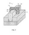
- a substrate 100includes a first semiconductor material S 1 .
- the substrate 100may be, for example, a bulk Si wafer, a bulk germanium (Ge) wafer, a semiconductor-on-insulator (SOI) substrate, or a strained semiconductor-on-insulator (SSOI) substrate.
- the substrate 100may include or consist essentially of the first semiconductor material, such as a group IV element, e.g., Ge or Si, a III-V compound, or a II-VI compound.
- substrate 100includes or consists essentially of (100) Si.
- a dielectric layer 110is formed over the semiconductor substrate 100 .
- the dielectric layer 110may include or consist essentially of a dielectric material, such as silicon nitride (Si 3 N 4 ) or silicon dioxide (SiO 2 ).
- the dielectric layer 110may be formed by any suitable technique, e.g., thermal oxidation or PECVD.
- the dielectric layermay have a thickness t 1 corresponding to a desired height h of crystalline material to be deposited in a trench formed through the dielectric layer.
- the thickness t 1 of the dielectric layer 110may be in the range of, e.g., 25-1000 nm.
- a mask(not shown), such as a photoresist mask, is formed over the substrate 100 and the dielectric layer 110 .
- the maskis patterned to expose at least a portion of the dielectric layer 110 .
- the exposed portion of the dielectric layer 110is removed by, e.g., reactive ion etching (RIE) to define a defect trapping region, e.g., trench 120 .
- Trench 120extends to a surface of the substrate 100 and may be defined by at least one sidewall 130 .
- the height h of the sidewall 130corresponds to the thickness t 1 of the dielectric layer 110 , and may be at least equal to a predetermined vertical distance H from a top surface 135 of the substrate, calculated as described below.
- the predetermined vertical distance H necessary to trap defectsis, typically, approximately equal to a width between 1 ⁇ 2 w and 2 w, where w is the width of the trench. This range is based on the range of intersection angles of approximately 30 degrees through 60 degrees; then, tan(30°)w ⁇ H ⁇ tan(60°)w, which roughly corresponds to 1 ⁇ 2 w ⁇ H ⁇ 2 w.
- the trenchmay be substantially rectangular in terms of cross-sectional profile, a top view, or both, and have a width w that is smaller than a length l of the trench.
- the width w of the trenchmay be less than about 500 nm, e.g., about 10-100 nm, and the length l of the trench may exceed each of w and H.
- the ratio of the height h of the trench to the width w of the trench 120may be ⁇ 0.5, e.g., ⁇ 1.
- a crystalline material 140is formed in the trench 120 .
- the crystalline material 140may include or consist essentially of a group IV element or compound, a III-V compound, or a II-VI compound.
- suitable group IV elements or compoundsinclude Ge, Si, SiGe, and SiC.
- suitable III-V compoundsinclude gallium arsenide (GaAs), gallium nitride (GaN), InAs, InSb, InAlSb, AlSb, indium aluminum arsenide (InAlAs), indium phosphide (InP), and InGaAs.
- suitable II-VI compoundsinclude CdSe, ZnTe, and CdTe.
- the crystalline material 140may be formed by selective epitaxial growth in any suitable epitaxial deposition system, including, but not limited to, metal-organic chemical vapor deposition (MOCVD), atmospheric-pressure CVD (APCVD), low- (or reduced-) pressure CVD (LPCVD), ultra-high-vacuum CVD (UHCVD), molecular beam epitaxy (MBE), or atomic layer deposition (ALD).
- MOCVDmetal-organic chemical vapor deposition
- APCVDatmospheric-pressure CVD
- LPCVDlow- (or reduced-) pressure CVD
- UHCVDultra-high-vacuum CVD
- MBEmolecular beam epitaxy
- ALDatomic layer deposition
- selective epitaxial growthtypically includes introducing a source gas into the chamber.
- the source gasmay include at least one precursor gas and a carrier gas, such as, for example, hydrogen.
- the reactor chambermay be heated by, for example, RF-heating.
- the growth temperature in the chamber
- the epitaxial growth systemmay be a single-wafer or multiple-wafer batch reactor.
- Suitable CVD systems commonly used for volume epitaxy in manufacturing applicationsinclude, for example, an Aixtron 2600 multi-wafer system available from Aixtron, based in Aachen, Germany; an EPI CENTURA single-wafer multi-chamber systems available from Applied Materials of Santa Clara, Calif.; or an EPSILON single-wafer epitaxial reactor available from ASM International based in Bilthoven, The Netherlands.
- Dislocation defects 150 in the crystalline material 140reach and terminate at the sidewalls of the trench 120 in the dielectric material 110 at or below the predetermined vertical distance H from the surface 135 of the substrate, such that dislocations in the crystalline material 140 decrease in density with increasing distance from the bottom portion of the trench 120 . Accordingly, the upper portion of the crystalline material is substantially exhausted of dislocation defects. Various dislocation defects such as threading dislocations, stacking faults, twin boundaries, or anti-phase boundaries may thus be substantially eliminated from the upper portion of the crystalline material.
- a planarization stepsuch as, e.g., CMP may be used to ensure that the top surface of the crystalline material 140 is substantially co-planar with the top surface of the dielectric material 110 .
- a portion of the dielectric layer 110is selectively removed to expose a side portion 200 of the crystalline material 140 .
- a height h channel of the exposed side portion 200may be equivalent to the thickness of a channel region to be formed.
- the portion of the dielectric layer 110is removed by an isotropic etch, e.g., a wet etch employing, for example, HF.
- a dry etchmay also be used, e.g., a plasma etch employing CF 4 and H 2 .
- the crystalline material 140may be considered as having two portions: a lower portion for trapping dislocation defects and an upper portion for a channel portion of a tri-gate MOSFET incorporating the crystalline material 140 .
- the height h of the crystalline materialthus has two components: the height h trapping of the lower portion (where defects are concentrated) and the height h channel of the upper portion (which is largely free of defects).
- the height h trapping of the trapping portionmay be selected from a range of about 1 ⁇ 2 w ⁇ h trapping ⁇ 2 w, to ensure effective trapping of dislocation defects.
- the actual value of h trapping requiredmay depend upon the type of dislocation defects encountered, which, in turn, may depend on the materials used, and also upon the orientation of the trench sidewalls.
- the height h trappingneed not be greater than that required for effective defect trapping, in order to ensure that the dislocation defects are trapped at a sufficient distance away from the channel portion. In this way, the deleterious effects of dislocation defects upon device performance are not experienced.
- h trappingmay be, e.g., 10-100 nm greater than required for effective trapping of defects.
- the height h channelmay typically be selected from the range of approximately 1 ⁇ 2 w ⁇ h channel ⁇ 10 w. In some cases, if h channel is significantly less than 1 ⁇ 2 w, the device may no longer be considered a multi-gate device, i.e., if conduction occurs primarily on the top surface of the gates disposed over the channel portion. If h channel is significantly greater than 10 w, subsequent device processing may be challenging, for example, because of possible mechanical instability of the fin during processing, or because of challenges in implanting ions in sidewalls of closely packed devices that include tall fins.
- a gate 210is defined over the crystalline material 140 by deposition and selective removal of a gate dielectric material 220 and a conductive gate material 230 .
- the gate dielectric materialmay be, e.g., SiO 2 , Si 3 N 4 , HfO 2 , HfSiON, and/or HfSiO.
- the conductive gate material 230may be, for example, polysilicon, amorphous Si, Ge, or SiGe gate material, or a metal or metal alloy.
- gate 210has three portions, one on each exposed side portion of the crystalline material 140 and one on a top surface of the crystalline material 140 .
- a source and a drainmay be defined in source and drain regions 240 , 250 of the crystalline material 140 proximate to the gate 210 and next to a channel 260 disposed under the gate 210 .
- the resulting structureis a tri-gate MOSFET 270 , employing the benefits of aspect ratio trapping (“ART”).
- ARTrefers generally to the technique(s) of causing defects in a material to terminate on a side surface as the material grows vertically, e.g., at a dielectric sidewall, with the sidewall being sufficiently high with respect to a width of the growth area, such that it traps most, if not all, of the defects.
- the crystalline material 140includes a first layer 300 and a second layer 310 .
- the first layer 300includes a second semiconductor material S 2
- the second layer 310includes a third semiconductor material S 3 .
- Each of the semiconductor material S 2 , S 3may include or consist essentially of one or more of a group IV element or compound, a III-V compound, or a II-VI compound.
- suitable group IV elements or compoundsinclude Ge, SiGe, and SiC.
- suitable III-V compoundsinclude GaAs, GaN, InAs, InSb, InAlSb, AlSb, InAlAs, rip, and InGaAs.
- suitable II-VI compoundsinclude CdSe, ZnTe, and CdTe.
- the second and third semiconductor materials S 2 , S 3may be different materials having different lattice constants.
- the lattice mismatchmay be selected from a range of, e.g., 0.2-4.0%. If the lattice mismatch is too low, the benefit to performance may not be significant. If the lattice mismatch is too high, the allowable thickness of the third semiconductor material S 3 may be too limited, if gross relaxation of third semiconductor material S 3 is to be avoided.
- the second semiconductor material S 2may be relaxed and the third semiconductor material S 3 may be strained.
- the second semiconductor material S 2includes or consists essentially of relaxed SiGe
- the third semiconductor material S 3includes or consists essentially of Si. This combination results in tensile strain in the channel 260 .
- the strainmay be primarily uniaxial in the direction of current flow due to lateral elastic relaxation. This type of strain is particularly beneficial for n-type metal-oxide-semiconductor (NMOS) device performance.
- NMOSmetal-oxide-semiconductor
- the second semiconductor materialincludes or consists essentially of relaxed SiGe
- the third semiconductor material S 3includes or consists essentially of Ge.
- the strainmay be primarily uniaxial in the direction of current flow due to lateral elastic relaxation. This type of strain is particularly beneficial for p-type metal-oxide-semiconductor (PMOS) device performance.
- PMOSmetal-oxide-semiconductor
- the resulting tri-gate MOSFET 270 or FinFET( FIG. 4 ) includes dielectric layer 110 disposed over the semiconductor substrate 100 including the first semiconductor material S 1 .
- Trench 120is disposed in the dielectric layer 110 , extends to the surface 135 of the substrate 100 , and is defined by at least one sidewall 130 .
- the sidewall 130has a height h at least equal to a predetermined distance H from the surface of the substrate.
- the trenchis substantially rectangular and has a width w.
- Crystalline material 140is at least partially disposed in the trench.
- the crystalline materialcomprises a first layer 300 that includes a second semiconductor material, and a second layer 310 that includes a third semiconductor material. A side portion of the second layer extends above the dielectric layer.
- Gate 210is disposed over the crystalline material.
- a ratio of the height h of the trench to the width w of the trenchis preferably ⁇ 0.5, dislocation defects in the crystalline material terminate at the sidewall of the trench at or below the predetermined distance H, h ⁇ H, and the third semiconductor material defines a strained channel 260 .
- a height h S2 of the first layer 300may be approximately equal to h trapping
- a height h s3 of the second layer 310may be approximately equal to h channel , with h trapping and h channel being determined as discussed above with reference to FIG. 2 .
- the height of the first layer h s2 and the height of the second layer h s3may be selected so that the second semiconductor material S 2 is relaxed and the third semiconductor material S 3 is strained, or vice versa.
- the second and third semiconductor materials S 2 , S 3may be selected to allow the formation of a bi-layer tri-gate device with high-mobility channel material and suppressed junction leakage.
- the second semiconductor material S 2may have a bandgap of at least 0.5 eV.
- the second semiconductor material S 2may include or consist essentially of a III-V material and/or a II-VI material, such as AlSb, InAlSb, GaSb, CdSe, ZnTe, and/or CdTe.
- the third semiconductor material S 3may have a high bulk electron mobility, e.g., greater than 2000 cm 2 /V ⁇ s. Materials that are suitable for NMOS and have high mobilities include, e.g., InSb, InAs, and InGaAs.
- the second semiconductor material S 2 and the third semiconductor material S 3have similar lattice constants. Matching lattice constants helps avoid significant defect formation at an interface 400 between these two materials, while also allowing a sufficient height h S3 (e.g., 20-200 nm) of the second layer 310 to make this layer suitable for use as a MOS channel.
- the difference between the lattice constant of the second semiconductor material and the lattice constant of the third semiconductor materialis less than 1%.
- a source and a drainare defined in source and drain regions 240 , 250 , respectively.
- bottom portions of the source and the drainare disposed in second semiconductor material S 2 , such that the relatively high bandgap of second semiconductor material S 2 helps limit junction leakage.
- an alternative process sequence for creating trench 120begins with formation of a mask (not shown) over semiconductor substrate 100 .
- a portion of the semiconductor substrate 100is removed to define a fin 500 .
- Fin 500may have dimensions substantially identically to the dimensions of trench 120 .
- Dielectric layer 110is deposited over the semiconductor substrate 100 and the fin 500 .
- the dielectric layer 110is then planarized by, e.g., chemical-mechanical polishing (CMP) such that a top surface of the dielectric layer is substantially co-planar with a top surface 510 of the fin 500 .
- CMPchemical-mechanical polishing
- Trench 120is defined by removing at least a portion of the fin 500 .
- the finmay be selectively removed with a wet or dry etch that removes semiconductor material S 1 with respect to the dielectric layer 110 .
- a wet or dry etchthat removes semiconductor material S 1 with respect to the dielectric layer 110 .
- semiconductor material S 1primarily comprises Si
- dielectric layer 110primarily comprises SiO 2
- a dry etch utilizing Cl 2 and/or HBrmay be used to selectively remove the Si.
- the etchmay be a timed etch, thereby avoiding undercutting a bottom portion of the dielectric layer 110 .
- trench 120is defined by at least one sidewall having a height h at least equal to a predetermined distance H from the bottom of the trench.
- the trenchmay be substantially rectangular and have a width w.
- the ratio of the height h of the trench to the width w of the trenchis preferably ⁇ 1, dislocation defects in the crystalline material terminate at the sidewall of the trench at or below the predetermined distance H, and h ⁇ H.
- a crystalline material 140is formed in the trench.
- the crystalline materialincludes second semiconductor material S 2 .
- a portion of the dielectric layer 110is removed to expose a side portion of the crystalline material.
- a gate dielectric 220 and a gate 210are formed over the second semiconductor material S 2 , to define a FinFET.
Landscapes
- Insulated Gate Type Field-Effect Transistor (AREA)
Abstract
Description
Claims (23)
Priority Applications (4)
| Application Number | Priority Date | Filing Date | Title |
|---|---|---|---|
| US11/861,931US7799592B2 (en) | 2006-09-27 | 2007-09-26 | Tri-gate field-effect transistors formed by aspect ratio trapping |
| US12/856,402US7977706B2 (en) | 2006-09-27 | 2010-08-13 | Tri-gate field-effect transistors formed by aspect ratio trapping |
| US13/107,483US8309986B2 (en) | 2006-09-27 | 2011-05-13 | Tri-gate field-effect transistors formed by aspect ratio trapping |
| US13/649,729US8628989B2 (en) | 2006-09-27 | 2012-10-11 | Tri-gate field-effect transistors formed by aspect ration trapping |
Applications Claiming Priority (2)
| Application Number | Priority Date | Filing Date | Title |
|---|---|---|---|
| US84742406P | 2006-09-27 | 2006-09-27 | |
| US11/861,931US7799592B2 (en) | 2006-09-27 | 2007-09-26 | Tri-gate field-effect transistors formed by aspect ratio trapping |
Related Child Applications (1)
| Application Number | Title | Priority Date | Filing Date |
|---|---|---|---|
| US12/856,402DivisionUS7977706B2 (en) | 2006-09-27 | 2010-08-13 | Tri-gate field-effect transistors formed by aspect ratio trapping |
Publications (2)
| Publication Number | Publication Date |
|---|---|
| US20080073667A1 US20080073667A1 (en) | 2008-03-27 |
| US7799592B2true US7799592B2 (en) | 2010-09-21 |
Family
ID=38920931
Family Applications (4)
| Application Number | Title | Priority Date | Filing Date |
|---|---|---|---|
| US11/861,931Active2029-01-20US7799592B2 (en) | 2006-09-27 | 2007-09-26 | Tri-gate field-effect transistors formed by aspect ratio trapping |
| US12/856,402ActiveUS7977706B2 (en) | 2006-09-27 | 2010-08-13 | Tri-gate field-effect transistors formed by aspect ratio trapping |
| US13/107,483ActiveUS8309986B2 (en) | 2006-09-27 | 2011-05-13 | Tri-gate field-effect transistors formed by aspect ratio trapping |
| US13/649,729ActiveUS8628989B2 (en) | 2006-09-27 | 2012-10-11 | Tri-gate field-effect transistors formed by aspect ration trapping |
Family Applications After (3)
| Application Number | Title | Priority Date | Filing Date |
|---|---|---|---|
| US12/856,402ActiveUS7977706B2 (en) | 2006-09-27 | 2010-08-13 | Tri-gate field-effect transistors formed by aspect ratio trapping |
| US13/107,483ActiveUS8309986B2 (en) | 2006-09-27 | 2011-05-13 | Tri-gate field-effect transistors formed by aspect ratio trapping |
| US13/649,729ActiveUS8628989B2 (en) | 2006-09-27 | 2012-10-11 | Tri-gate field-effect transistors formed by aspect ration trapping |
Country Status (2)
| Country | Link |
|---|---|
| US (4) | US7799592B2 (en) |
| WO (1) | WO2008039495A1 (en) |
Cited By (71)
| Publication number | Priority date | Publication date | Assignee | Title |
|---|---|---|---|---|
| US20090140294A1 (en)* | 2007-11-30 | 2009-06-04 | Hemant Adhikari | hetero-structured, inverted-t field effect transistor |
| US20090261380A1 (en)* | 2008-04-17 | 2009-10-22 | Brent Alan Anderson | Transistors having asymetric strained source/drain portions |
| US20090321882A1 (en)* | 2008-06-03 | 2009-12-31 | Amberwave Systems Corporation | Epitazial growth of crystalline material |
| US20100252836A1 (en)* | 2007-11-27 | 2010-10-07 | Sophia School Corporation | Group-iii nitride structure and method for producing a group-iii nitride structure |
| US20110147847A1 (en)* | 2009-12-21 | 2011-06-23 | Cea Stephen M | Methods and apparatus to reduce layout based strain variations in non-planar transistor structures |
| US20110180806A1 (en)* | 2010-01-28 | 2011-07-28 | Intersil Americas Inc. | Monolithic integration of gallium nitride and silicon devices and circuits, structure and method |
| US20110193175A1 (en)* | 2010-02-09 | 2011-08-11 | Taiwan Semiconductor Manufacturing Co., Ltd. | Lower parasitic capacitance finfet |
| US8216951B2 (en) | 2006-09-27 | 2012-07-10 | Taiwan Semiconductor Manufacturing Company, Ltd. | Quantum tunneling devices and circuits with lattice-mismatched semiconductor structures |
| US8237151B2 (en) | 2009-01-09 | 2012-08-07 | Taiwan Semiconductor Manufacturing Company, Ltd. | Diode-based devices and methods for making the same |
| US8253211B2 (en) | 2008-09-24 | 2012-08-28 | Taiwan Semiconductor Manufacturing Company, Ltd. | Semiconductor sensor structures with reduced dislocation defect densities |
| US20120224419A1 (en)* | 2011-03-02 | 2012-09-06 | Kabushiki Kaisha Toshiba | Semiconductor storage device |
| US8274097B2 (en) | 2008-07-01 | 2012-09-25 | Taiwan Semiconductor Manufacturing Company, Ltd. | Reduction of edge effects from aspect ratio trapping |
| US8304805B2 (en) | 2009-01-09 | 2012-11-06 | Taiwan Semiconductor Manufacturing Company, Ltd. | Semiconductor diodes fabricated by aspect ratio trapping with coalesced films |
| US8324660B2 (en) | 2005-05-17 | 2012-12-04 | Taiwan Semiconductor Manufacturing Company, Ltd. | Lattice-mismatched semiconductor structures with reduced dislocation defect densities and related methods for device fabrication |
| US8329541B2 (en) | 2007-06-15 | 2012-12-11 | Taiwan Semiconductor Manufacturing Company, Ltd. | InP-based transistor fabrication |
| US8344242B2 (en) | 2007-09-07 | 2013-01-01 | Taiwan Semiconductor Manufacturing Company, Ltd. | Multi-junction solar cells |
| US8377759B2 (en)* | 2010-08-17 | 2013-02-19 | International Business Machines Corporation | Controlled fin-merging for fin type FET devices |
| US8384196B2 (en) | 2008-09-19 | 2013-02-26 | Taiwan Semiconductor Manufacturing Company, Ltd. | Formation of devices by epitaxial layer overgrowth |
| US20130119347A1 (en)* | 2011-11-15 | 2013-05-16 | Samsung Electronics Co., Ltd. | Semiconductor device including group iii-v barrier and method of manufacturing the semiconductor device |
| US8502263B2 (en) | 2006-10-19 | 2013-08-06 | Taiwan Semiconductor Manufacturing Company, Ltd. | Light-emitter-based devices with lattice-mismatched semiconductor structures |
| US20130234204A1 (en)* | 2012-03-06 | 2013-09-12 | Samsung Electronics Co., Ltd. | Fin field effect transistors including multiple lattice constants and methods of fabricating the same |
| US20130295752A1 (en)* | 2012-05-04 | 2013-11-07 | Applied Materials, Inc. | Methods for chemical mechanical planarization of patterned wafers |
| US8624103B2 (en) | 2007-04-09 | 2014-01-07 | Taiwan Semiconductor Manufacturing Company, Ltd. | Nitride-based multi-junction solar cell modules and methods for making the same |
| US8629446B2 (en) | 2009-04-02 | 2014-01-14 | Taiwan Semiconductor Manufacturing Company, Ltd. | Devices formed from a non-polar plane of a crystalline material and method of making the same |
| KR101401274B1 (en)* | 2013-02-26 | 2014-05-29 | 연세대학교 산학협력단 | Finfet device using ge and/or iii-v group compound semiconductor and method of manufacturing the same |
| KR101410092B1 (en)* | 2012-03-08 | 2014-06-25 | 타이완 세미콘덕터 매뉴팩쳐링 컴퍼니 리미티드 | Semiconductor structures and methods with high mobility and high energy bandgap materials |
| KR20140091754A (en)* | 2011-12-21 | 2014-07-22 | 인텔 코오퍼레이션 | Methods for forming fins for metal oxide semiconductor device structures |
| US20140220751A1 (en)* | 2013-02-01 | 2014-08-07 | Taiwan Semiconductor Manufacturing Company, Ltd. | Methods for Forming Semiconductor Regions in Trenches |
| US20140252478A1 (en)* | 2013-03-08 | 2014-09-11 | Taiwan Semiconductor Manufacturing Company, Ltd. | FinFET with Channel Backside Passivation Layer Device and Method |
| US20140264592A1 (en)* | 2013-03-12 | 2014-09-18 | Taiwan Semiconductor Manufacturing Co. Ltd. | Barrier Layer for FinFET Channels |
| US8847279B2 (en) | 2006-09-07 | 2014-09-30 | Taiwan Semiconductor Manufacturing Company, Ltd. | Defect reduction using aspect ratio trapping |
| CN104124273A (en)* | 2013-04-26 | 2014-10-29 | 台湾积体电路制造股份有限公司 | MOS devices with strain buffer layer and methods of forming the same |
| KR101456773B1 (en) | 2012-04-11 | 2014-10-31 | 타이완 세미콘덕터 매뉴팩쳐링 컴퍼니 리미티드 | Semiconductor device channel system and method |
| US8878243B2 (en) | 2006-03-24 | 2014-11-04 | Taiwan Semiconductor Manufacturing Company, Ltd. | Lattice-mismatched semiconductor structures and related methods for device fabrication |
| US20140342533A1 (en)* | 2013-05-15 | 2014-11-20 | Applied Materials, Inc. | Method of strain and defect control in thin semiconductor films |
| US8937299B2 (en) | 2013-03-13 | 2015-01-20 | International Business Machines Corporation | III-V finFETs on silicon substrate |
| US8981427B2 (en) | 2008-07-15 | 2015-03-17 | Taiwan Semiconductor Manufacturing Company, Ltd. | Polishing of small composite semiconductor materials |
| US9087903B2 (en) | 2013-04-26 | 2015-07-21 | Taiwan Semiconductor Manufacturing Company, Ltd. | Buffer layer omega gate |
| US9093531B2 (en) | 2013-06-11 | 2015-07-28 | Taiwan Semiconductor Manufacturing Company, Ltd. | Fin structure of semiconductor device |
| US9123363B2 (en) | 2012-12-18 | 2015-09-01 | Seagate Technology Llc | Crystalline magnetic layer to amorphous substrate bonding |
| US9129889B2 (en) | 2013-03-15 | 2015-09-08 | Semiconductor Components Industries, Llc | High electron mobility semiconductor device and method therefor |
| US20150279938A1 (en)* | 2012-11-16 | 2015-10-01 | SK Hynix Inc. | Semiconductor device and method of manufacturing the same |
| US20150318354A1 (en)* | 2012-11-25 | 2015-11-05 | Institute of Microelectronics Chinese Academy of Science | Semiconductor device and manufacturing method therefor |
| US9196711B2 (en) | 2014-03-07 | 2015-11-24 | International Business Machines Corporation | Fin field effect transistor including self-aligned raised active regions |
| US9202915B2 (en) | 2009-10-30 | 2015-12-01 | Taiwan Semiconductor Manufacturing Company, Ltd. | Method of forming epi film in substrate trench |
| US9293530B1 (en) | 2014-11-14 | 2016-03-22 | International Business Machines Corporation | High aspect ratio trapping semiconductor with uniform height and isolated from bulk substrate |
| US9318491B2 (en) | 2014-02-28 | 2016-04-19 | Samsung Electronics Co., Ltd. | Semiconductor fin devices and method of fabricating the semiconductor fin devices |
| US9349809B1 (en) | 2014-11-14 | 2016-05-24 | International Business Machines Corporation | Aspect ratio trapping and lattice engineering for III/V semiconductors |
| US9379243B1 (en)* | 2015-02-19 | 2016-06-28 | Intermational Business Machines Corporation | Field-effect transistor with aggressively strained fins |
| US9391134B2 (en) | 2013-07-31 | 2016-07-12 | Samsung Electronics Co., Ltd. | Fin field effect transistor, semiconductor device including the same and method of forming the semiconductor device |
| US9508890B2 (en) | 2007-04-09 | 2016-11-29 | Taiwan Semiconductor Manufacturing Company, Ltd. | Photovoltaics on silicon |
| US20160365362A1 (en)* | 2015-04-30 | 2016-12-15 | Taiwan Semiconductor Manufacturing Company, Ltd. | FETS and Methods of Forming FETS |
| US9547740B2 (en) | 2011-05-05 | 2017-01-17 | Synopsys, Inc. | Methods for fabricating high-density integrated circuit devices |
| US9564373B2 (en) | 2015-02-27 | 2017-02-07 | International Business Machines Corporation | Forming a CMOS with dual strained channels |
| US9570359B2 (en) | 2013-10-31 | 2017-02-14 | Samsung Electronics Co., Ltd. | Substrate structure, complementary metal oxide semiconductor device, and method of manufacturing complementary metal oxide semiconductor device |
| US9590041B1 (en) | 2015-10-30 | 2017-03-07 | United Microelectronics Corp. | Semiconductor structure |
| US20170104070A1 (en)* | 2015-10-08 | 2017-04-13 | United Microelectronics Corp. | Semiconductor device and method for fabricating the same |
| US9634007B2 (en) | 2012-09-28 | 2017-04-25 | Intel Corporation | Trench confined epitaxially grown device layer(s) |
| US9773910B2 (en) | 2015-11-04 | 2017-09-26 | United Microelectronics Corp. | Semiconductor structure and manufacturing method thereof |
| US9859426B1 (en) | 2016-06-29 | 2018-01-02 | International Business Machines Corporation | Semiconductor device including optimized elastic strain buffer |
| US9859381B2 (en) | 2005-05-17 | 2018-01-02 | Taiwan Semiconductor Manufacturing Company, Ltd. | Lattice-mismatched semiconductor structures with reduced dislocation defect densities and related methods for device fabrication |
| US9960163B2 (en) | 2016-03-22 | 2018-05-01 | United Microelectronics Corp. | Method for fabricating fin-shaped structure and bump made of different material |
| US9984872B2 (en) | 2008-09-19 | 2018-05-29 | Taiwan Semiconductor Manufacturing Company, Ltd. | Fabrication and structures of crystalline material |
| US10068963B2 (en) | 2015-10-02 | 2018-09-04 | United Microelectronics Corp. | Fin-type field effect transistor and method of forming the same |
| US10084085B2 (en) | 2015-06-11 | 2018-09-25 | Taiwan Semiconductor Manufacturing Co., Ltd. | Fin field effect transistor (FinFET) device structure with stop layer and method for forming the same |
| US10164109B2 (en) | 2014-10-17 | 2018-12-25 | Taiwan Semiconductor Manufacturing Co., Ltd. | Fin field effect transistor (FinFET) device and method for forming the same |
| US10497797B2 (en) | 2015-10-26 | 2019-12-03 | United Microelectronics Corp. | Semiconductor structure and manufacturing method thereof |
| US11101348B2 (en) | 2018-07-25 | 2021-08-24 | Globalfoundries U.S. Inc. | Nanosheet field effect transistor with spacers between sheets |
| US11342441B2 (en) | 2012-07-17 | 2022-05-24 | Unm Rainforest Innovations | Method of forming a seed area and growing a heteroepitaxial layer on the seed area |
| US11670686B2 (en)* | 2017-09-26 | 2023-06-06 | Intel Corporation | III-N nanostructures formed via cavity fill |
| US12062703B2 (en) | 2015-11-17 | 2024-08-13 | Tessera Llc | Self aligned replacement metal source/drain FINFET |
Families Citing this family (121)
| Publication number | Priority date | Publication date | Assignee | Title |
|---|---|---|---|---|
| EP2595175B1 (en)* | 2005-05-17 | 2019-04-17 | Taiwan Semiconductor Manufacturing Company, Ltd. | Method of fabricating a lattice-mismatched semiconductor structure with reduced dislocation defect densities |
| KR101329388B1 (en)* | 2005-07-26 | 2013-11-14 | 앰버웨이브 시스템즈 코포레이션 | Solutions for integrated circuit integration of alternative active area materials |
| US20070054467A1 (en)* | 2005-09-07 | 2007-03-08 | Amberwave Systems Corporation | Methods for integrating lattice-mismatched semiconductor structure on insulators |
| US7638842B2 (en)* | 2005-09-07 | 2009-12-29 | Amberwave Systems Corporation | Lattice-mismatched semiconductor structures on insulators |
| US20080070355A1 (en)* | 2006-09-18 | 2008-03-20 | Amberwave Systems Corporation | Aspect ratio trapping for mixed signal applications |
| JP2008159972A (en)* | 2006-12-26 | 2008-07-10 | Elpida Memory Inc | Semiconductor device and manufacturing method thereof |
| US7674669B2 (en)* | 2007-09-07 | 2010-03-09 | Micron Technology, Inc. | FIN field effect transistor |
| US8440517B2 (en)* | 2010-10-13 | 2013-05-14 | Taiwan Semiconductor Manufacturing Company, Ltd. | FinFET and method of fabricating the same |
| US9601328B2 (en) | 2009-10-08 | 2017-03-21 | Taiwan Semiconductor Manufacturing Company, Ltd. | Growing a III-V layer on silicon using aligned nano-scale patterns |
| DE102010038742B4 (en)* | 2010-07-30 | 2016-01-21 | Globalfoundries Dresden Module One Llc & Co. Kg | Method and semiconductor device based on a deformation technology in three-dimensional transistors based on a deformed channel semiconductor material |
| US8558279B2 (en)* | 2010-09-23 | 2013-10-15 | Intel Corporation | Non-planar device having uniaxially strained semiconductor body and method of making same |
| US8062963B1 (en) | 2010-10-08 | 2011-11-22 | Taiwan Semiconductor Manufacturing Company, Ltd. | Method of fabricating a semiconductor device having an epitaxy region |
| US20120153352A1 (en)* | 2010-12-15 | 2012-06-21 | Gilbert Dewey | High indium content transistor channels |
| US8889494B2 (en) | 2010-12-29 | 2014-11-18 | Globalfoundries Singapore Pte. Ltd. | Finfet |
| US8492235B2 (en) | 2010-12-29 | 2013-07-23 | Globalfoundries Singapore Pte. Ltd. | FinFET with stressors |
| CN102790006B (en)* | 2011-05-17 | 2014-09-17 | 中国科学院微电子研究所 | Semiconductor structure and manufacturing method thereof |
| US9761666B2 (en)* | 2011-06-16 | 2017-09-12 | Taiwan Semiconductor Manufacturing Company, Ltd. | Strained channel field effect transistor |
| US9105660B2 (en)* | 2011-08-17 | 2015-08-11 | United Microelectronics Corp. | Fin-FET and method of forming the same |
| US8643108B2 (en)* | 2011-08-19 | 2014-02-04 | Altera Corporation | Buffered finFET device |
| US8723236B2 (en)* | 2011-10-13 | 2014-05-13 | Taiwan Semiconductor Manufacturing Company, Ltd. | FinFET device and method of manufacturing same |
| US8624326B2 (en)* | 2011-10-20 | 2014-01-07 | Taiwan Semiconductor Manufacturing Company, Ltd. | FinFET device and method of manufacturing same |
| US9099388B2 (en)* | 2011-10-21 | 2015-08-04 | Taiwan Semiconductor Manufacturing Company, Ltd. | III-V multi-channel FinFETs |
| KR101867999B1 (en) | 2011-10-31 | 2018-06-18 | 삼성전자주식회사 | Method of forming III-V group material layer, semiconductor device comprising III-V group material layer and method of manufacturing the same |
| CN103137671B (en)* | 2011-12-02 | 2015-06-24 | 中芯国际集成电路制造(上海)有限公司 | Multi-grid field effect transistor and manufacturing method thereof |
| US9281378B2 (en)* | 2012-01-24 | 2016-03-08 | Taiwan Semiconductor Manufacturing Company, Ltd. | Fin recess last process for FinFET fabrication |
| US9171925B2 (en) | 2012-01-24 | 2015-10-27 | Taiwan Semiconductor Manufacturing Company, Ltd. | Multi-gate devices with replaced-channels and methods for forming the same |
| US9466696B2 (en) | 2012-01-24 | 2016-10-11 | Taiwan Semiconductor Manufacturing Company, Ltd. | FinFETs and methods for forming the same |
| US20130193492A1 (en)* | 2012-01-30 | 2013-08-01 | International Business Machines Corporation | Silicon carbon film structure and method |
| US20130200455A1 (en)* | 2012-02-08 | 2013-08-08 | Taiwan Semiconductor Manufacturing Company, Ltd. | Dislocation smt for finfet device |
| JP6207170B2 (en) | 2012-02-15 | 2017-10-04 | アイメックImec | Mask structure and method for defect-free heteroepitaxial |
| CN103295902A (en)* | 2012-03-02 | 2013-09-11 | 中芯国际集成电路制造(上海)有限公司 | Finned field-effect tube and forming method thereof |
| US8673704B2 (en)* | 2012-05-09 | 2014-03-18 | Institute of Microelectronics, Chinese Academy of Sciences | FinFET and method for manufacturing the same |
| US8680576B2 (en)* | 2012-05-16 | 2014-03-25 | Taiwan Semiconductor Manufacturing Company, Ltd. | CMOS device and method of forming the same |
| KR101922107B1 (en) | 2012-06-22 | 2019-02-13 | 삼성전자주식회사 | Semiconductor device and method of manufacturing the same |
| CN103579295B (en)* | 2012-07-25 | 2016-12-28 | 中国科学院微电子研究所 | Semiconductor device and method for manufacturing the same |
| US9728464B2 (en)* | 2012-07-27 | 2017-08-08 | Intel Corporation | Self-aligned 3-D epitaxial structures for MOS device fabrication |
| CN103579004B (en)* | 2012-08-10 | 2016-05-11 | 中国科学院微电子研究所 | Finfet and manufacturing method thereof |
| US20140061792A1 (en)* | 2012-08-28 | 2014-03-06 | International Business Machines Corporation | Field effect transistor devices with recessed gates |
| EP2709156A3 (en)* | 2012-09-14 | 2014-04-23 | Imec | Band engineered semiconductor device and method for manufacturing thereof |
| US8716751B2 (en)* | 2012-09-28 | 2014-05-06 | Intel Corporation | Methods of containing defects for non-silicon device engineering |
| EP2717316B1 (en)* | 2012-10-05 | 2019-08-14 | IMEC vzw | Method for producing strained germanium fin structures |
| CN103811344B (en) | 2012-11-09 | 2016-08-10 | 中国科学院微电子研究所 | Semiconductor device and method for manufacturing the same |
| US9443962B2 (en)* | 2012-11-09 | 2016-09-13 | Taiwan Semiconductor Manufacturing Company, Ltd. | Recessing STI to increase fin height in fin-first process |
| US9349837B2 (en)* | 2012-11-09 | 2016-05-24 | Taiwan Semiconductor Manufacturing Company, Ltd. | Recessing STI to increase Fin height in Fin-first process |
| US8866235B2 (en)* | 2012-11-09 | 2014-10-21 | Taiwan Semiconductor Manufacturing Company, Ltd. | Source and drain dislocation fabrication in FinFETs |
| EP2741320B1 (en)* | 2012-12-05 | 2020-06-17 | IMEC vzw | Manufacturing method of a finfet device with dual-strained channels |
| US9299809B2 (en)* | 2012-12-17 | 2016-03-29 | Globalfoundries Inc. | Methods of forming fins for a FinFET device wherein the fins have a high germanium content |
| US8896101B2 (en) | 2012-12-21 | 2014-11-25 | Intel Corporation | Nonplanar III-N transistors with compositionally graded semiconductor channels |
| US9123633B2 (en) | 2013-02-01 | 2015-09-01 | Taiwan Semiconductor Manufacturing Company, Ltd. | Methods for forming semiconductor regions in trenches |
| US9184233B2 (en)* | 2013-02-27 | 2015-11-10 | Taiwan Semiconductor Manufacturing Company, Ltd. | Structure and method for defect passivation to reduce junction leakage for finFET device |
| US9087902B2 (en)* | 2013-02-27 | 2015-07-21 | Taiwan Semiconductor Manufacturing Company, Ltd. | FinFETs with strained well regions |
| EP2775528B1 (en)* | 2013-03-05 | 2019-07-17 | IMEC vzw | Passivated III-V or Ge fin-shaped field effect transistor |
| US9385198B2 (en)* | 2013-03-12 | 2016-07-05 | Taiwan Semiconductor Manufacturing Company, Ltd. | Heterostructures for semiconductor devices and methods of forming the same |
| US9293534B2 (en)* | 2014-03-21 | 2016-03-22 | Taiwan Semiconductor Manufacturing Company, Ltd. | Formation of dislocations in source and drain regions of FinFET devices |
| US9293466B2 (en) | 2013-06-19 | 2016-03-22 | Taiwan Semiconductor Manufacturing Company, Ltd. | Embedded SRAM and methods of forming the same |
| US8952420B1 (en) | 2013-07-29 | 2015-02-10 | Stmicroelectronics, Inc. | Method to induce strain in 3-D microfabricated structures |
| US8916445B1 (en) | 2013-08-16 | 2014-12-23 | International Business Machines Corporation | Semiconductor devices and methods of manufacture |
| EP2849219A1 (en)* | 2013-09-11 | 2015-03-18 | IMEC vzw | Method for manufacturing transistors and associated substrate |
| US9099559B2 (en) | 2013-09-16 | 2015-08-04 | Stmicroelectronics, Inc. | Method to induce strain in finFET channels from an adjacent region |
| CN105493251A (en)* | 2013-09-27 | 2016-04-13 | 英特尔公司 | Non-planar semiconductor device with multi-layer flexible substrate |
| EP2866264A1 (en) | 2013-10-22 | 2015-04-29 | IMEC vzw | Method for manufacturing a field effect transistor of a non-planar type |
| US9484423B2 (en) | 2013-11-01 | 2016-11-01 | Samsung Electronics Co., Ltd. | Crystalline multiple-nanosheet III-V channel FETs |
| US9570609B2 (en) | 2013-11-01 | 2017-02-14 | Samsung Electronics Co., Ltd. | Crystalline multiple-nanosheet strained channel FETs and methods of fabricating the same |
| WO2015099692A1 (en)* | 2013-12-23 | 2015-07-02 | Intel Corporation | Tensile source drain iii-v transistors for mobility improved n-mos |
| US9177967B2 (en)* | 2013-12-24 | 2015-11-03 | Intel Corporation | Heterogeneous semiconductor material integration techniques |
| US9324717B2 (en)* | 2013-12-28 | 2016-04-26 | Texas Instruments Incorporated | High mobility transistors |
| US9590090B2 (en) | 2014-01-08 | 2017-03-07 | Taiwan Semiconductor Manufacturing Company Limited | Method of forming channel of gate structure |
| US9214557B2 (en)* | 2014-02-06 | 2015-12-15 | Globalfoundries Singapore Pte. Ltd. | Device with isolation buffer |
| US9287115B2 (en) | 2014-03-12 | 2016-03-15 | International Business Machines Corporation | Planar III-V field effect transistor (FET) on dielectric layer |
| WO2015147851A1 (en)* | 2014-03-28 | 2015-10-01 | Intel Corporation | Strain compensation in transistors |
| US9299587B2 (en) | 2014-04-10 | 2016-03-29 | Taiwan Semiconductor Manufacturing Company, Ltd. | Microwave anneal (MWA) for defect recovery |
| US9391140B2 (en)* | 2014-06-20 | 2016-07-12 | Globalfoundries Inc. | Raised fin structures and methods of fabrication |
| FR3023058B1 (en)* | 2014-06-30 | 2017-09-29 | Commissariat Energie Atomique | METHOD FOR PRODUCING A MICROELECTRONIC DEVICE |
| US9263555B2 (en)* | 2014-07-03 | 2016-02-16 | Globalfoundries Inc. | Methods of forming a channel region for a semiconductor device by performing a triple cladding process |
| US9647098B2 (en) | 2014-07-21 | 2017-05-09 | Samsung Electronics Co., Ltd. | Thermionically-overdriven tunnel FETs and methods of fabricating the same |
| KR102202754B1 (en)* | 2014-08-14 | 2021-01-15 | 삼성전자주식회사 | Semiconductor device |
| EP3195368A4 (en)* | 2014-09-19 | 2018-05-16 | Intel Corporation | Apparatus and methods to create a doped sub-structure to reduce leakage in microelectronic transistors |
| WO2016043770A1 (en)* | 2014-09-19 | 2016-03-24 | Intel Corporation | Apparatus and methods to create a buffer to reduce leakage in microelectronic transistors |
| WO2016043769A1 (en) | 2014-09-19 | 2016-03-24 | Intel Corporation | Apparatus and methods to create an indium gallium arsenide active channel having indium rich surfaces |
| US9349808B2 (en) | 2014-09-29 | 2016-05-24 | International Business Machines Corporation | Double aspect ratio trapping |
| US9601377B2 (en)* | 2014-10-17 | 2017-03-21 | Taiwan Semiconductor Manufacturing Company, Ltd. | FinFET formation process and structure |
| US9349594B1 (en) | 2014-11-05 | 2016-05-24 | International Business Machines Corporation | Non-planar semiconductor device with aspect ratio trapping |
| EP3018715B1 (en) | 2014-11-05 | 2024-10-23 | IMEC vzw | Method for manufacturing a transistor device comprising a germanium channel material on a silicon based substrate |
| US9312143B1 (en) | 2014-11-24 | 2016-04-12 | International Business Machines Corporation | Formation of isolation surrounding well implantation |
| US9530701B2 (en) | 2014-12-18 | 2016-12-27 | International Business Machines Corporation | Method of forming semiconductor fins on SOI substrate |
| US10497814B2 (en) | 2014-12-23 | 2019-12-03 | Intel Corporation | III-V semiconductor alloys for use in the subfin of non-planar semiconductor devices and methods of forming the same |
| EP3238267A4 (en)* | 2014-12-23 | 2018-09-05 | Intel Corporation | Thin channel region on wide subfin |
| US20170317187A1 (en)* | 2014-12-23 | 2017-11-02 | Intel Corporation | Uniform Layers Formed with Aspect Ratio Trench Based Processes |
| EP3238268A4 (en)* | 2014-12-24 | 2018-12-26 | Intel Corporation | Apparatus and methods of forming fin structures with asymmetric profile |
| US9362278B1 (en)* | 2014-12-29 | 2016-06-07 | Taiwan Semiconductor Manufacturing Company, Ltd. | FinFET with multiple dislocation planes and method for forming the same |
| KR102274750B1 (en)* | 2015-01-27 | 2021-07-07 | 삼성전자주식회사 | Method for fabricating semiconductor device |
| US10026659B2 (en)* | 2015-01-29 | 2018-07-17 | Globalfoundries Inc. | Methods of forming fin isolation regions under tensile-strained fins on FinFET semiconductor devices |
| US9543439B2 (en)* | 2015-01-30 | 2017-01-10 | Taiwan Semiconductor Manufacturing Company Ltd. | Semiconductor device structure and manufacturing method thereof |
| US9548319B2 (en) | 2015-03-10 | 2017-01-17 | International Business Machines Corporation | Structure for integration of an III-V compound semiconductor on SOI |
| US9608067B2 (en) | 2015-03-30 | 2017-03-28 | International Business Machines Corporation | Hybrid aspect ratio trapping |
| CN107636834B (en)* | 2015-06-16 | 2021-11-09 | 英特尔公司 | Transistor with sub-fin layer |
| US9496401B1 (en)* | 2015-06-30 | 2016-11-15 | International Business Machines Corpoartion | III-V device structure with multiple threshold voltage |
| WO2017044117A1 (en) | 2015-09-11 | 2017-03-16 | Intel Corporation | Aluminum indium phosphide subfin germanium channel transistors |
| US9601482B1 (en) | 2015-12-08 | 2017-03-21 | International Business Machines Corporation | Economical and environmentally friendly chemical mechanical polishing for III-V compound semiconductor device fabrication |
| US10615161B2 (en) | 2016-02-08 | 2020-04-07 | International Business Machines Corporation | III-V fins by aspect ratio trapping and self-aligned etch to remove rough epitaxy surface |
| TWI717338B (en) | 2016-03-08 | 2021-02-01 | 聯華電子股份有限公司 | Semiconductor device and method for fabricating the same |
| WO2017171875A1 (en)* | 2016-04-01 | 2017-10-05 | Intel Corporation | An indium-containing fin of a transistor device with an indium-rich core |
| US9905645B2 (en)* | 2016-05-24 | 2018-02-27 | Samsung Electronics Co., Ltd. | Vertical field effect transistor having an elongated channel |
| US10249736B2 (en) | 2016-06-15 | 2019-04-02 | International Business Machines Corporation | Aspect ratio trapping in channel last process |
| US11276755B2 (en) | 2016-06-17 | 2022-03-15 | Intel Corporation | Field effect transistors with gate electrode self-aligned to semiconductor fin |
| US11152290B2 (en)* | 2016-06-29 | 2021-10-19 | Intel Corporatuon | Wide bandgap group IV subfin to reduce leakage |
| WO2018004632A1 (en)* | 2016-06-30 | 2018-01-04 | Intel Corporation | A finfet transistor having a tapered subfin structure |
| DE112016007023T5 (en) | 2016-06-30 | 2019-03-21 | Intel Corporation | A FINFET transistor having a doped sub-fin structure for reducing channel-to-substrate leakage |
| US10002759B2 (en)* | 2016-07-26 | 2018-06-19 | Applied Materials, Inc. | Method of forming structures with V shaped bottom on silicon substrate |
| CN106206318B (en)* | 2016-08-12 | 2019-06-11 | 中国科学院微电子研究所 | Fin type field effect transistor and preparation method thereof |
| US9728626B1 (en) | 2016-08-30 | 2017-08-08 | Globalfoundries Inc. | Almost defect-free active channel region |
| US11222982B2 (en)* | 2016-09-29 | 2022-01-11 | Intel Corporation | Methods and apparatus to form silicon-based transistors on group III-nitride materials using aspect ratio trapping |
| WO2018063360A1 (en)* | 2016-09-30 | 2018-04-05 | Intel Corporation | Strained silicon layer with relaxed underlayer |
| US9865589B1 (en)* | 2016-10-31 | 2018-01-09 | Taiwan Semiconductor Manufacturing Co., Ltd. | System and method of fabricating ESD FinFET with improved metal landing in the drain |
| KR102466356B1 (en)* | 2017-08-30 | 2022-11-15 | 삼성전자주식회사 | Semiconductor devices and method of fabricating the same |
| US10559504B2 (en) | 2018-02-20 | 2020-02-11 | International Business Machines Corporation | High mobility semiconductor fins on insulator |
| US11653488B2 (en) | 2020-05-07 | 2023-05-16 | Micron Technology, Inc. | Apparatuses including transistors, and related methods, memory devices, and electronic systems |
| US11735590B2 (en) | 2020-11-13 | 2023-08-22 | International Business Machines Corporation | Fin stack including tensile-strained and compressively strained fin portions |
| US11837604B2 (en) | 2021-09-22 | 2023-12-05 | International Business Machine Corporation | Forming stacked nanosheet semiconductor devices with optimal crystalline orientations around devices |
| US12191208B2 (en) | 2021-09-23 | 2025-01-07 | International Business Machines Corporation | Dual strained semiconductor substrate and patterning |
| US20240047207A1 (en)* | 2022-08-02 | 2024-02-08 | Infineon Technologies Ag | Technique for Forming Cubic Silicon Carbide and Heterojunction Silicon Carbide Device |
Citations (236)
| Publication number | Priority date | Publication date | Assignee | Title |
|---|---|---|---|---|
| US4545109A (en) | 1983-01-21 | 1985-10-08 | Rca Corporation | Method of making a gallium arsenide field effect transistor |
| US4551394A (en) | 1984-11-26 | 1985-11-05 | Honeywell Inc. | Integrated three-dimensional localized epitaxial growth of Si with localized overgrowth of GaAs |
| US4651179A (en) | 1983-01-21 | 1987-03-17 | Rca Corporation | Low resistance gallium arsenide field effect transistor |
| US4727047A (en) | 1980-04-10 | 1988-02-23 | Massachusetts Institute Of Technology | Method of producing sheets of crystalline material |
| US4774205A (en) | 1986-06-13 | 1988-09-27 | Massachusetts Institute Of Technology | Monolithic integration of silicon and gallium arsenide devices |
| US4789643A (en) | 1986-09-25 | 1988-12-06 | Mitsubishi Denki Kabushiki Kaisha | Method of manufacturing a heterojunction bipolar transistor involving etch and refill |
| US4826784A (en) | 1987-11-13 | 1989-05-02 | Kopin Corporation | Selective OMCVD growth of compound semiconductor materials on silicon substrates |
| US4860081A (en) | 1984-06-28 | 1989-08-22 | Gte Laboratories Incorporated | Semiconductor integrated circuit structure with insulative partitions |
| US4876210A (en) | 1987-04-30 | 1989-10-24 | The University Of Delaware | Solution growth of lattice mismatched and solubility mismatched heterostructures |
| JPH0262090A (en)* | 1988-08-29 | 1990-03-01 | Matsushita Electric Ind Co Ltd | Method for manufacturing optical semiconductor devices |
| US4948456A (en) | 1989-06-09 | 1990-08-14 | Delco Electronics Corporation | Confined lateral selective epitaxial growth |
| US5032893A (en) | 1988-04-01 | 1991-07-16 | Cornell Research Foundation, Inc. | Method for reducing or eliminating interface defects in mismatched semiconductor eiplayers |
| US5034337A (en) | 1989-02-10 | 1991-07-23 | Texas Instruments Incorporated | Method of making an integrated circuit that combines multi-epitaxial power transistors with logic/analog devices |
| US5061644A (en) | 1988-12-22 | 1991-10-29 | Honeywell Inc. | Method for fabricating self-aligned semiconductor devices |
| US5091767A (en) | 1991-03-18 | 1992-02-25 | At&T Bell Laboratories | Article comprising a lattice-mismatched semiconductor heterostructure |
| US5091333A (en) | 1983-09-12 | 1992-02-25 | Massachusetts Institute Of Technology | Reducing dislocations in semiconductors utilizing repeated thermal cycling during multistage epitaxial growth |
| US5093699A (en) | 1990-03-12 | 1992-03-03 | Texas A & M University System | Gate adjusted resonant tunnel diode device and method of manufacture |
| US5098850A (en) | 1989-06-16 | 1992-03-24 | Canon Kabushiki Kaisha | Process for producing substrate for selective crystal growth, selective crystal growth process and process for producing solar battery by use of them |
| US5105247A (en) | 1990-08-03 | 1992-04-14 | Cavanaugh Marion E | Quantum field effect device with source extension region formed under a gate and between the source and drain regions |
| US5156995A (en) | 1988-04-01 | 1992-10-20 | Cornell Research Foundation, Inc. | Method for reducing or eliminating interface defects in mismatched semiconductor epilayers |
| US5166767A (en) | 1987-04-14 | 1992-11-24 | National Semiconductor Corporation | Sidewall contact bipolar transistor with controlled lateral spread of selectively grown epitaxial layer |
| US5236546A (en) | 1987-01-26 | 1993-08-17 | Canon Kabushiki Kaisha | Process for producing crystal article |
| US5238869A (en) | 1988-07-25 | 1993-08-24 | Texas Instruments Incorporated | Method of forming an epitaxial layer on a heterointerface |
| US5256594A (en) | 1989-06-16 | 1993-10-26 | Intel Corporation | Masking technique for depositing gallium arsenide on silicon |
| US5269876A (en) | 1987-01-26 | 1993-12-14 | Canon Kabushiki Kaisha | Process for producing crystal article |
| US5269852A (en) | 1991-05-27 | 1993-12-14 | Canon Kabushiki Kaisha | Crystalline solar cell and method for producing the same |
| US5281283A (en) | 1987-03-26 | 1994-01-25 | Canon Kabushiki Kaisha | Group III-V compound crystal article using selective epitaxial growth |
| US5285086A (en) | 1990-08-02 | 1994-02-08 | At&T Bell Laboratories | Semiconductor devices with low dislocation defects |
| US5295150A (en) | 1992-12-11 | 1994-03-15 | Eastman Kodak Company | Distributed feedback-channeled substrate planar semiconductor laser |
| US5403751A (en) | 1990-11-29 | 1995-04-04 | Canon Kabushiki Kaisha | Process for producing a thin silicon solar cell |
| US5417180A (en) | 1991-10-24 | 1995-05-23 | Rohm Co., Ltd. | Method for forming SOI structure |
| US5427976A (en) | 1991-03-27 | 1995-06-27 | Nec Corporation | Method of producing a semiconductor on insulating substrate, and a method of forming a transistor thereon |
| US5432120A (en) | 1992-12-04 | 1995-07-11 | Siemens Aktiengesellschaft | Method for producing a laterally limited single-crystal region with selective epitaxy and the employment thereof for manufacturing a bipolar transistor as well as a MOS transistor |
| US5438018A (en) | 1992-12-07 | 1995-08-01 | Fujitsu Limited | Method of making semiconductor device by selective epitaxial growth |
| US5518953A (en) | 1991-09-24 | 1996-05-21 | Rohm Co., Ltd. | Method for manufacturing semiconductor device having grown layer on insulating layer |
| US5589696A (en) | 1991-10-15 | 1996-12-31 | Nec Corporation | Tunnel transistor comprising a semiconductor film between gate and source/drain |
| US5621227A (en) | 1995-07-18 | 1997-04-15 | Discovery Semiconductors, Inc. | Method and apparatus for monolithic optoelectronic integrated circuit using selective epitaxy |
| US5640022A (en) | 1993-08-27 | 1997-06-17 | Sanyo Electric Co., Inc. | Quantum effect device |
| US5710436A (en) | 1994-09-27 | 1998-01-20 | Kabushiki Kaisha Toshiba | Quantum effect device |
| US5717709A (en) | 1993-06-04 | 1998-02-10 | Sharp Kabushiki Kaisha | Semiconductor light-emitting device capable of having good stability in fundamental mode of oscillation, decreasing current leakage, and lowering oscillation threshold limit, and method of making the same |
| US5792679A (en) | 1993-08-30 | 1998-08-11 | Sharp Microelectronics Technology, Inc. | Method for forming silicon-germanium/Si/silicon dioxide heterostructure using germanium implant |
| US5825049A (en) | 1996-10-09 | 1998-10-20 | Sandia Corporation | Resonant tunneling device with two-dimensional quantum well emitter and base layers |
| US5849077A (en) | 1994-04-11 | 1998-12-15 | Texas Instruments Incorporated | Process for growing epitaxial silicon in the windows of an oxide-patterned wafer |
| US5886385A (en) | 1996-08-22 | 1999-03-23 | Kabushiki Kaisha Toshiba | Semiconductor device and manufacturing method thereof |
| US5953361A (en) | 1995-05-31 | 1999-09-14 | Siemens Aktiengesellschaft | DFB laser diode structure having complex optical grating coupling |
| US5966620A (en) | 1996-11-15 | 1999-10-12 | Canon Kabshiki Kaisha | Process for producing semiconductor article |
| US6011271A (en) | 1994-04-28 | 2000-01-04 | Fujitsu Limited | Semiconductor device and method of fabricating the same |
| US6015979A (en) | 1997-08-29 | 2000-01-18 | Kabushiki Kaisha Toshiba | Nitride-based semiconductor element and method for manufacturing the same |
| US6049098A (en) | 1995-04-27 | 2000-04-11 | Nec Corporation | Bipolar transistor having an emitter region formed of silicon carbide |
| US6100106A (en) | 1997-11-17 | 2000-08-08 | Nec Corporation | Fabrication of nitride semiconductor light-emitting device |
| US6111288A (en) | 1997-03-18 | 2000-08-29 | Kabushiki Kaisha Toshiba | Quantum tunneling effect device and semiconductor composite substrate |
| JP2000286449A (en) | 1999-03-31 | 2000-10-13 | Toyoda Gosei Co Ltd | Iii nitride compound semiconductor device and its manufacture |
| US6191432B1 (en) | 1996-09-02 | 2001-02-20 | Kabushiki Kaisha Toshiba | Semiconductor device and memory device |
| US6228691B1 (en) | 1999-06-30 | 2001-05-08 | Intel Corp. | Silicon-on-insulator devices and method for producing the same |
| US6252261B1 (en) | 1998-09-30 | 2001-06-26 | Nec Corporation | GaN crystal film, a group III element nitride semiconductor wafer and a manufacturing process therefor |
| US20010006249A1 (en) | 1997-09-16 | 2001-07-05 | Eugene A Fitzgerald | Co-planar si and ge composite substrate and method of producing same |
| US6271551B1 (en) | 1995-12-15 | 2001-08-07 | U.S. Philips Corporation | Si-Ge CMOS semiconductor device |
| US20010045604A1 (en) | 2000-05-25 | 2001-11-29 | Hitachi, Ltd. | Semiconductor device and manufacturing method |
| US6342404B1 (en) | 1999-03-31 | 2002-01-29 | Toyoda Gosei Co., Ltd. | Group III nitride compound semiconductor device and method for producing |
| US6348096B1 (en) | 1997-03-13 | 2002-02-19 | Nec Corporation | Method for manufacturing group III-V compound semiconductors |
| US20020030246A1 (en) | 2000-06-28 | 2002-03-14 | Motorola, Inc. | Structure and method for fabricating semiconductor structures and devices not lattice matched to the substrate |
| US6362071B1 (en) | 2000-04-05 | 2002-03-26 | Motorola, Inc. | Method for forming a semiconductor device with an opening in a dielectric layer |
| US6407425B1 (en) | 2000-09-21 | 2002-06-18 | Texas Instruments Incorporated | Programmable neuron MOSFET on SOI |
| US20020084000A1 (en)* | 1997-06-24 | 2002-07-04 | Eugene A. Fitzgerald | Controlling threading dislocation densities in Ge on Si using graded GeSi layers and planarization |
| US6475869B1 (en) | 2001-02-26 | 2002-11-05 | Advanced Micro Devices, Inc. | Method of forming a double gate transistor having an epitaxial silicon/germanium channel region |
| US6492216B1 (en) | 2002-02-07 | 2002-12-10 | Taiwan Semiconductor Manufacturing Company | Method of forming a transistor with a strained channel |
| US6512252B1 (en) | 1999-11-15 | 2003-01-28 | Matsushita Electric Industrial Co., Ltd. | Semiconductor device |
| US20030030117A1 (en) | 2001-05-22 | 2003-02-13 | Hitachi, Ltd. | Semiconductor device |
| US6521514B1 (en) | 1999-11-17 | 2003-02-18 | North Carolina State University | Pendeoepitaxial methods of fabricating gallium nitride semiconductor layers on sapphire substrates |
| US20030045017A1 (en) | 2001-09-06 | 2003-03-06 | Kazumasa Hiramatsu | Method for fabricating III-V Group compound semiconductor |
| US20030064535A1 (en) | 2001-09-28 | 2003-04-03 | Kub Francis J. | Method of manufacturing a semiconductor device having a thin GaN material directly bonded to an optimized substrate |
| US20030087462A1 (en) | 2001-11-02 | 2003-05-08 | Norikatsu Koide | Semiconductor light emitting device and method for producing the same |
| US20030089899A1 (en) | 2000-08-22 | 2003-05-15 | Lieber Charles M. | Nanoscale wires and related devices |
| US6576532B1 (en) | 2001-11-30 | 2003-06-10 | Motorola Inc. | Semiconductor device and method therefor |
| US6579463B1 (en) | 2000-08-18 | 2003-06-17 | The Regents Of The University Of Colorado | Tunable nanomasks for pattern transfer and nanocluster array formation |
| US6603172B1 (en) | 1996-06-17 | 2003-08-05 | Matsushita Electric Industrial Co., Ltd. | Semiconductor device and method of manufacturing the same |
| US20030155586A1 (en) | 1999-05-21 | 2003-08-21 | Toyoda Gosei Co., Ltd. | Methods and devices using group III nitride compound semiconductor |
| US6617643B1 (en) | 2002-06-28 | 2003-09-09 | Mcnc | Low power tunneling metal-oxide-semiconductor (MOS) device |
| US20030178677A1 (en) | 2002-03-19 | 2003-09-25 | International Business Machines Corporation | Strained fin fets structure and method |
| US6635110B1 (en) | 1999-06-25 | 2003-10-21 | Massachusetts Institute Of Technology | Cyclic thermal anneal for dislocation reduction |
| US20030207518A1 (en) | 1999-10-14 | 2003-11-06 | Hua-Shuang Kong | Single step pendeo- and lateral epitaxial overgrowth of Group III-nitride epitaxial layers with Group III-nitride buffer layer and resulting structures |
| US20040012037A1 (en) | 2002-07-18 | 2004-01-22 | Motorola, Inc. | Hetero-integration of semiconductor materials on silicon |
| US6686245B1 (en) | 2002-12-20 | 2004-02-03 | Motorola, Inc. | Vertical MOSFET with asymmetric gate structure |
| US6710368B2 (en) | 2001-10-01 | 2004-03-23 | Ken Scott Fisher | Quantum tunneling transistor |
| US6720196B2 (en) | 2001-05-11 | 2004-04-13 | Sanyo Electric Co., Ltd. | Nitride-based semiconductor element and method of forming nitride-based semiconductor |
| US20040072410A1 (en) | 1997-10-30 | 2004-04-15 | Kensaku Motoki | GaN single crystal substrate and method of making the same |
| US20040075105A1 (en) | 2002-08-23 | 2004-04-22 | Amberwave Systems Corporation | Semiconductor heterostructures having reduced dislocation pile-ups and related methods |
| US6727523B2 (en) | 1999-12-16 | 2004-04-27 | Sony Corporation | Method of manufacturing crystal of iii-v compounds of the nitride system, crystal substrate of iii-v compounds of the nitride system, crystal film of iii-v compounds of the nitride system, and method of manufacturing device |
| US6762483B1 (en) | 2003-01-23 | 2004-07-13 | Advanced Micro Devices, Inc. | Narrow fin FinFET |
| JP2004200375A (en) | 2002-12-18 | 2004-07-15 | Matsushita Electric Ind Co Ltd | Semiconductor laser device and method of manufacturing the same |
| US6784074B2 (en) | 2001-05-09 | 2004-08-31 | Nsc-Nanosemiconductor Gmbh | Defect-free semiconductor templates for epitaxial growth and method of making same |
| US6787864B2 (en) | 2002-09-30 | 2004-09-07 | Advanced Micro Devices, Inc. | Mosfets incorporating nickel germanosilicided gate and methods for their formation |
| US6794718B2 (en) | 2002-12-19 | 2004-09-21 | International Business Machines Corporation | High mobility crystalline planes in double-gate CMOS technology |
| US6800910B2 (en) | 2002-09-30 | 2004-10-05 | Advanced Micro Devices, Inc. | FinFET device incorporating strained silicon in the channel region |
| US20040195624A1 (en) | 2003-04-04 | 2004-10-07 | National Taiwan University | Strained silicon fin field effect transistor |
| US6803598B1 (en) | 1999-05-07 | 2004-10-12 | University Of Delaware | Si-based resonant interband tunneling diodes and method of making interband tunneling diodes |
| US6809351B2 (en) | 2001-03-07 | 2004-10-26 | Nec Corporation | Group III-V compound semiconductor crystal structure and method of epitaxial growth of the same as well as semiconductor device including the same |
| US6812495B2 (en) | 2002-06-19 | 2004-11-02 | Massachusetts Institute Of Technology | Ge photodetectors |
| US6815241B2 (en) | 2002-09-25 | 2004-11-09 | Cao Group, Inc. | GaN structures having low dislocation density and methods of manufacture |
| US6815738B2 (en) | 2003-02-28 | 2004-11-09 | International Business Machines Corporation | Multiple gate MOSFET structure with strained Si Fin body |
| US20040227187A1 (en) | 2003-02-13 | 2004-11-18 | Zhiyuan Cheng | Integrated semiconductor device and method to make same |
| US6825534B2 (en) | 1999-06-04 | 2004-11-30 | International Business Machines Corporation | Semiconductor device on a combination bulk silicon and silicon-on-insulator (SOI) substrate |
| US6835246B2 (en) | 2001-11-16 | 2004-12-28 | Saleem H. Zaidi | Nanostructures for hetero-expitaxial growth on silicon substrates |
| US6835618B1 (en) | 2003-08-05 | 2004-12-28 | Advanced Micro Devices, Inc. | Epitaxially grown fin for FinFET |
| US6838322B2 (en) | 2003-05-01 | 2005-01-04 | Freescale Semiconductor, Inc. | Method for forming a double-gated semiconductor device |
| US20050003572A1 (en) | 2003-04-30 | 2005-01-06 | Osram Opto Semiconductors Gmbh | Method for fabricating a plurality of semiconductor chips |
| US6841410B2 (en) | 2001-09-03 | 2005-01-11 | Nec Corporation | Method for forming group-III nitride semiconductor layer and group-III nitride semiconductor device |
| US6841808B2 (en) | 2000-06-23 | 2005-01-11 | Toyoda Gosei Co., Ltd. | Group III nitride compound semiconductor device and method for producing the same |
| US20050017351A1 (en) | 2003-06-30 | 2005-01-27 | Ravi Kramadhati V. | Silicon on diamond wafers and devices |
| US6849487B2 (en) | 2003-05-27 | 2005-02-01 | Motorola, Inc. | Method for forming an electronic structure using etch |
| WO2005013375A1 (en) | 2003-08-05 | 2005-02-10 | Fujitsu Limited | Semiconductor device and its manufacturing method |
| US6855982B1 (en) | 2004-02-02 | 2005-02-15 | Advanced Micro Devices, Inc. | Self aligned double gate transistor having a strained channel region and process therefor |
| US6855583B1 (en) | 2003-08-05 | 2005-02-15 | Advanced Micro Devices, Inc. | Method for forming tri-gate FinFET with mesa isolation |
| US6855990B2 (en) | 2002-11-26 | 2005-02-15 | Taiwan Semiconductor Manufacturing Co., Ltd | Strained-channel multiple-gate transistor |
| US20050040444A1 (en) | 2003-08-22 | 2005-02-24 | International Business Machines Corporation | Strained-channel fin field effect transistor (FET) with a uniform channel thickness and separate gates |
| US20050045983A1 (en) | 2003-07-28 | 2005-03-03 | Takafumi Noda | Semiconductor device and method for manufacturing the same |
| US20050054180A1 (en) | 2003-09-09 | 2005-03-10 | Sang Han | Threading-dislocation-free nanoheteroepitaxy of Ge on Si using self-directed touch-down of Ge through a thin SiO2 layer |
| US20050054164A1 (en) | 2003-09-09 | 2005-03-10 | Advanced Micro Devices, Inc. | Strained silicon MOSFETs having reduced diffusion of n-type dopants |
| US6867433B2 (en) | 2003-04-30 | 2005-03-15 | Taiwan Semiconductor Manufacturing Company, Ltd. | Semiconductor-on-insulator chip incorporating strained-channel partially-depleted, fully-depleted, and multiple-gate transistors |
| US6873009B2 (en) | 1999-05-13 | 2005-03-29 | Hitachi, Ltd. | Vertical semiconductor device with tunnel insulator in current path controlled by gate electrode |
| US20050073028A1 (en)* | 2003-10-02 | 2005-04-07 | Grant John M. | Semiconductor device incorporating a defect controlled strained channel structure and method of making the same |
| US6887773B2 (en) | 2002-06-19 | 2005-05-03 | Luxtera, Inc. | Methods of incorporating germanium within CMOS process |
| US6888181B1 (en) | 2004-03-18 | 2005-05-03 | United Microelectronics Corp. | Triple gate device having strained-silicon channel |
| US20050093154A1 (en) | 2003-07-25 | 2005-05-05 | Interuniversitair Microelektronica Centrum (Imec Vzw) | Multiple gate semiconductor device and method for forming same |
| US20050093021A1 (en) | 2003-10-31 | 2005-05-05 | Ouyang Qiqing C. | High mobility heterojunction complementary field effect transistors and methods thereof |
| US20050104156A1 (en) | 2003-11-13 | 2005-05-19 | Texas Instruments Incorporated | Forming a semiconductor structure in manufacturing a semiconductor device using one or more epitaxial growth processes |
| US20050104152A1 (en) | 2003-09-19 | 2005-05-19 | Snyder John P. | Schottky barrier integrated circuit |
| WO2005048330A1 (en) | 2003-11-12 | 2005-05-26 | Advancesis Limited | Formation of lattice-tuning semiconductor substrates |
| US6900070B2 (en) | 2002-04-15 | 2005-05-31 | The Regents Of The University Of California | Dislocation reduction in non-polar gallium nitride thin films |
| US6900502B2 (en) | 2003-04-03 | 2005-05-31 | Taiwan Semiconductor Manufacturing Company, Ltd. | Strained channel on insulator device |
| US20050118825A1 (en) | 2002-02-28 | 2005-06-02 | Kazuki Nishijima | Process for producing group III nitride compound semiconductor |
| US20050118793A1 (en) | 2003-10-03 | 2005-06-02 | Snyder John P. | Schottky-barrier MOSFET manufacturing method using isotropic etch process |
| US6902965B2 (en) | 2003-10-31 | 2005-06-07 | Taiwan Semiconductor Manufacturing Company, Ltd. | Strained silicon structure |
| US6902991B2 (en) | 2002-10-24 | 2005-06-07 | Advanced Micro Devices, Inc. | Semiconductor device having a thick strained silicon layer and method of its formation |
| US20050127451A1 (en) | 2003-12-05 | 2005-06-16 | Yoshinori Tsuchiya | Semiconductor device |
| US6909186B2 (en) | 2003-05-01 | 2005-06-21 | International Business Machines Corporation | High performance FET devices and methods therefor |
| US20050139860A1 (en) | 2003-10-22 | 2005-06-30 | Snyder John P. | Dynamic schottky barrier MOSFET device and method of manufacture |
| EP1551063A1 (en) | 2002-06-04 | 2005-07-06 | Nitride Semiconductors Co., Ltd. | Gallium nitride compound semiconductor device and manufacturing method |
| US20050145954A1 (en) | 2004-01-05 | 2005-07-07 | International Business Machines Corporation | Structures and methods for making strained mosfets |
| US20050145941A1 (en) | 2004-01-07 | 2005-07-07 | International Business Machines Corporation | High performance strained silicon FinFETs device and method for forming same |
| US6917068B1 (en) | 2002-06-21 | 2005-07-12 | Advanced Micro Devices, Inc. | Semiconductor device having conductive structures formed near a gate electrode |
| US6920159B2 (en) | 2002-11-29 | 2005-07-19 | Optitune Plc | Tunable optical source |
| US20050156202A1 (en) | 2004-01-17 | 2005-07-21 | Hwa-Sung Rhee | At least penta-sided-channel type of FinFET transistor |
| US6921982B2 (en) | 2003-07-21 | 2005-07-26 | International Business Machines Corporation | FET channel having a strained lattice structure along multiple surfaces |
| US6921673B2 (en) | 2001-03-27 | 2005-07-26 | Sony Corporation | Nitride semiconductor device and method of manufacturing the same |
| US20050164475A1 (en) | 2004-01-23 | 2005-07-28 | Martin Peckerar | Technique for perfecting the active regions of wide bandgap semiconductor nitride devices |
| US20050181549A1 (en) | 2004-02-17 | 2005-08-18 | Barr Alexander L. | Semiconductor structure having strained semiconductor and method therefor |
| US20050184302A1 (en) | 2000-04-04 | 2005-08-25 | Toshimasa Kobayashi | Nitride semiconductor device and method of manufacturing the same |
| US6936875B2 (en) | 2002-10-02 | 2005-08-30 | Renesas Technology Corp. | Insulated-gate field-effect transistor, method of fabricating same, and semiconductor device employing same |
| US6943407B2 (en) | 2003-06-17 | 2005-09-13 | International Business Machines Corporation | Low leakage heterojunction vertical transistors and high performance devices thereof |
| US6946683B2 (en) | 2002-01-28 | 2005-09-20 | Nichia Corporation | Opposed terminal structure having a nitride semiconductor element |
| US20050205859A1 (en) | 2003-03-07 | 2005-09-22 | Amberwave Systems Corporation | Shallow trench isolation process |
| US6949769B2 (en) | 2002-09-17 | 2005-09-27 | Taiwan Semiconductor Manufacturing Company, Ltd. | Suppression of MOSFET gate leakage current |
| US20050212051A1 (en) | 2003-04-16 | 2005-09-29 | Sarnoff Corporation | Low voltage silicon controlled rectifier (SCR) for electrostatic discharge (ESD) protection of silicon-on-insulator technologies |
| US20050217565A1 (en) | 2002-05-28 | 2005-10-06 | Hacene Lahreche | Method for epitaxial growth of a gallium nitride film separated from its substrate |
| US6955969B2 (en) | 2003-09-03 | 2005-10-18 | Advanced Micro Devices, Inc. | Method of growing as a channel region to reduce source/drain junction capacitance |
| WO2005098963A1 (en) | 2004-03-31 | 2005-10-20 | Intel Corporation | A bulk non-planar transistor having a strained channel with enhanced mobility and methods of fabrication |
| US6958254B2 (en) | 2001-05-08 | 2005-10-25 | Btg International Limited | Method to produce germanium layers |
| US20050250285A1 (en)* | 2004-05-04 | 2005-11-10 | Jae-Man Yoon | Fin field effect transistor device and method of fabricating the same |
| US6974733B2 (en) | 2003-06-16 | 2005-12-13 | Intel Corporation | Double-gate transistor with enhanced carrier mobility |
| US6977194B2 (en) | 2003-10-30 | 2005-12-20 | International Business Machines Corporation | Structure and method to improve channel mobility by gate electrode stress modification |
| US6982204B2 (en) | 2002-07-16 | 2006-01-03 | Cree, Inc. | Nitride-based transistors and methods of fabrication thereof using non-etched contact recesses |
| US6984571B1 (en) | 1999-10-01 | 2006-01-10 | Ziptronix, Inc. | Three dimensional device integration method and integrated device |
| US20060019462A1 (en) | 2004-07-23 | 2006-01-26 | International Business Machines Corporation | Patterned strained semiconductor substrate and device |
| US6991998B2 (en) | 2004-07-02 | 2006-01-31 | International Business Machines Corporation | Ultra-thin, high quality strained silicon-on-insulator formed by elastic strain transfer |
| US6994751B2 (en) | 2001-02-27 | 2006-02-07 | Sanyo Electric Co., Ltd. | Nitride-based semiconductor element and method of forming nitride-based semiconductor |
| US6995456B2 (en) | 2004-03-12 | 2006-02-07 | International Business Machines Corporation | High-performance CMOS SOI devices on hybrid crystal-oriented substrates |
| US6995430B2 (en) | 2002-06-07 | 2006-02-07 | Amberwave Systems Corporation | Strained-semiconductor-on-insulator device structures |
| US6998684B2 (en) | 2004-03-31 | 2006-02-14 | International Business Machines Corporation | High mobility plane CMOS SOI |
| US7001804B2 (en) | 2004-01-30 | 2006-02-21 | Atmel Germany Gmbh | Method of producing active semiconductor layers of different thicknesses in an SOI wafer |
| US20060049409A1 (en) | 2002-12-18 | 2006-03-09 | Rafferty Conor S | Method for forming integrated circuit utilizing dual semiconductors |
| US7012314B2 (en) | 2002-12-18 | 2006-03-14 | Agere Systems Inc. | Semiconductor devices with reduced active region defects and unique contacting schemes |
| US7015497B1 (en) | 2002-08-27 | 2006-03-21 | The Ohio State University | Self-aligned and self-limited quantum dot nanoswitches and methods for making same |
| US7033936B1 (en) | 1999-08-17 | 2006-04-25 | Imperial Innovations Limited | Process for making island arrays |
| US7033436B2 (en) | 2001-04-12 | 2006-04-25 | Sony Corporation | Crystal growth method for nitride semiconductor and formation method for semiconductor device |
| US7041178B2 (en) | 2000-02-16 | 2006-05-09 | Ziptronix, Inc. | Method for low temperature bonding and bonded structure |
| US7045401B2 (en) | 2003-06-23 | 2006-05-16 | Sharp Laboratories Of America, Inc. | Strained silicon finFET device |
| US20060105533A1 (en) | 2004-11-16 | 2006-05-18 | Chong Yung F | Method for engineering hybrid orientation/material semiconductor substrate |
| US20060113603A1 (en) | 2004-12-01 | 2006-06-01 | Amberwave Systems Corporation | Hybrid semiconductor-on-insulator structures and related methods |
| US7061065B2 (en) | 2003-03-31 | 2006-06-13 | National Chung-Hsing University | Light emitting diode and method for producing the same |
| US20060128124A1 (en) | 2002-12-16 | 2006-06-15 | Haskell Benjamin A | Growth of reduced dislocation density non-polar gallium nitride by hydride vapor phase epitaxy |
| US20060131606A1 (en) | 2004-12-18 | 2006-06-22 | Amberwave Systems Corporation | Lattice-mismatched semiconductor structures employing seed layers and related fabrication methods |
| US20060145264A1 (en) | 2005-01-05 | 2006-07-06 | Internaional Business Machines Corporation | Stressed field effect transistors on hybrid orientation substrate |
| US7074623B2 (en) | 2002-06-07 | 2006-07-11 | Amberwave Systems Corporation | Methods of forming strained-semiconductor-on-insulator finFET device structures |
| US7078731B2 (en) | 2002-12-27 | 2006-07-18 | General Electric Company | Gallium nitride crystals and wafers and method of making |
| US7078299B2 (en) | 2003-09-03 | 2006-07-18 | Advanced Micro Devices, Inc. | Formation of finFET using a sidewall epitaxial layer |
| US20060160291A1 (en) | 2005-01-19 | 2006-07-20 | Sharp Laboratories Of America, Inc. | Integration of biaxial tensile strained NMOS and uniaxial compressive strained PMOS on the same wafer |
| US7084051B2 (en) | 2002-06-07 | 2006-08-01 | Sharp Kabushiki Kaisha | Manufacturing method for semiconductor substrate and manufacturing method for semiconductor device |
| US7084441B2 (en) | 2004-05-20 | 2006-08-01 | Cree, Inc. | Semiconductor devices having a hybrid channel layer, current aperture transistors and methods of fabricating same |
| US7087965B2 (en) | 2004-04-22 | 2006-08-08 | International Business Machines Corporation | Strained silicon CMOS on hybrid crystal orientations |
| US20060175601A1 (en) | 2000-08-22 | 2006-08-10 | President And Fellows Of Harvard College | Nanoscale wires and related devices |
| US7091561B2 (en) | 2003-06-13 | 2006-08-15 | Kabushiki Kaisha Toshiba | Field effect transistor and method of manufacturing the same |
| US7095043B2 (en) | 2003-06-18 | 2006-08-22 | Hitachi, Ltd. | Semiconductor device, semiconductor circuit module and manufacturing method of the same |
| US20060189056A1 (en) | 2003-08-12 | 2006-08-24 | Chih-Hsin Ko | Strained channel complementary field-effect transistors and methods of manufacture |
| US7098508B2 (en) | 2003-08-25 | 2006-08-29 | International Business Machines Corporation | Ultra-thin silicon-on-insulator and strained-silicon-direct-on-insulator with hybrid crystal orientations |
| US20060205197A1 (en) | 2005-03-09 | 2006-09-14 | Siltron Inc. | Compound semiconductor devices and methods of manufacturing the same |
| US20060202276A1 (en) | 2005-03-08 | 2006-09-14 | Seiko Epson Corporation | Semiconductor device and method of making semiconductor devices |
| US20060211210A1 (en) | 2004-08-27 | 2006-09-21 | Rensselaer Polytechnic Institute | Material for selective deposition and etching |
| US7118987B2 (en) | 2004-01-29 | 2006-10-10 | Taiwan Semiconductor Manufacturing Co., Ltd. | Method of achieving improved STI gap fill with reduced stress |
| US7119402B2 (en) | 2003-09-05 | 2006-10-10 | Kabushiki Kaisha Toshiba | Field effect transistor and manufacturing method thereof |
| US7125785B2 (en) | 2004-06-14 | 2006-10-24 | International Business Machines Corporation | Mixed orientation and mixed material semiconductor-on-insulator wafer |
| US7132691B1 (en) | 1998-09-10 | 2006-11-07 | Rohm Co., Ltd. | Semiconductor light-emitting device and method for manufacturing the same |
| US7138302B2 (en) | 2004-01-12 | 2006-11-21 | Advanced Micro Devices, Inc. | Method of fabricating an integrated circuit channel region |
| US7138292B2 (en) | 2003-09-10 | 2006-11-21 | Lsi Logic Corporation | Apparatus and method of manufacture for integrated circuit and CMOS device including epitaxially grown dielectric on silicon carbide |
| US20060267047A1 (en) | 2005-05-26 | 2006-11-30 | Matsushita Electric Industrial Co., Ltd. | Hetero-junction bipolar transistor and manufacturing method of the same |
| US20060292719A1 (en) | 2005-05-17 | 2006-12-28 | Amberwave Systems Corporation | Lattice-mismatched semiconductor structures with reduced dislocation defect densities and related methods for device fabrication |
| US7160753B2 (en) | 2004-03-16 | 2007-01-09 | Voxtel, Inc. | Silicon-on-insulator active pixel sensors |
| US7164183B2 (en) | 2003-06-09 | 2007-01-16 | Canon Kabushiki Kaisha | Semiconductor substrate, semiconductor device, and method of manufacturing the same |
| US20070029643A1 (en) | 2003-03-21 | 2007-02-08 | Johnson Mark A L | Methods for nanoscale structures from optical lithography and subsequent lateral growth |
| US7176522B2 (en) | 2003-11-25 | 2007-02-13 | Taiwan Semiconductor Manufacturing Company, Ltd. | Semiconductor device having high drive current and method of manufacturing thereof |
| US7180134B2 (en) | 2004-01-30 | 2007-02-20 | Taiwan Semiconductor Manufacturing Company, Ltd. | Methods and structures for planar and multiple-gate transistors formed on SOI |
| US20070054465A1 (en) | 2005-09-07 | 2007-03-08 | Amberwave Systems Corporation | Lattice-mismatched semiconductor structures on insulators |
| US20070054467A1 (en) | 2005-09-07 | 2007-03-08 | Amberwave Systems Corporation | Methods for integrating lattice-mismatched semiconductor structure on insulators |
| US7195993B2 (en) | 1998-06-10 | 2007-03-27 | North Carolina State University | Methods of fabricating gallium nitride semiconductor layers by lateral growth into trenches |
| US7198995B2 (en) | 2003-12-12 | 2007-04-03 | International Business Machines Corporation | Strained finFETs and method of manufacture |
| US7205604B2 (en) | 2001-03-13 | 2007-04-17 | International Business Machines Corporation | Ultra scalable high speed heterojunction vertical n-channel MISFETs and methods thereof |
| US7211864B2 (en) | 2003-09-15 | 2007-05-01 | Seliskar John J | Fully-depleted castellated gate MOSFET device and method of manufacture thereof |
| US20070105335A1 (en) | 2005-11-01 | 2007-05-10 | Massachusetts Institute Of Technology | Monolithically integrated silicon and III-V electronics |
| US7224033B2 (en) | 2005-02-15 | 2007-05-29 | International Business Machines Corporation | Structure and method for manufacturing strained FINFET |
| EP1796180A1 (en) | 2004-08-31 | 2007-06-13 | Akihiko Kikuchi | Light emitting element and its manufacturing method |
| US7244958B2 (en) | 2004-06-24 | 2007-07-17 | International Business Machines Corporation | Integration of strained Ge into advanced CMOS technology |
| US7247534B2 (en) | 2003-11-19 | 2007-07-24 | International Business Machines Corporation | Silicon device on Si:C-OI and SGOI and method of manufacture |
| US20070181977A1 (en) | 2005-07-26 | 2007-08-09 | Amberwave Systems Corporation | Solutions for integrated circuit integration of alternative active area materials |
| US20070187668A1 (en) | 2006-02-16 | 2007-08-16 | Takashi Noguchi | Crystal substrates and methods of fabricating the same |
| US20070196987A1 (en) | 2006-02-21 | 2007-08-23 | Dureseti Chidambarrao | Pseudomorphic Si/SiGe/Si body device with embedded SiGe source/drain |
| US7262117B1 (en) | 2003-06-10 | 2007-08-28 | Luxtera, Inc. | Germanium integrated CMOS wafer and method for manufacturing the same |
| US7268058B2 (en) | 2004-01-16 | 2007-09-11 | Intel Corporation | Tri-gate transistors and methods to fabricate same |
| US20070267722A1 (en) | 2006-05-17 | 2007-11-22 | Amberwave Systems Corporation | Lattice-mismatched semiconductor structures with reduced dislocation defect densities and related methods for device fabrication |
| US20080001169A1 (en) | 2006-03-24 | 2008-01-03 | Amberwave Systems Corporation | Lattice-mismatched semiconductor structures and related methods for device fabrication |
| US7344942B2 (en) | 2005-01-26 | 2008-03-18 | Micron Technology, Inc. | Isolation regions for semiconductor devices and their formation |
| US20080070355A1 (en) | 2006-09-18 | 2008-03-20 | Amberwave Systems Corporation | Aspect ratio trapping for mixed signal applications |
| US20080073641A1 (en) | 2006-09-27 | 2008-03-27 | Amberwave Systems Corporation | Quantum tunneling devices and circuits with lattice-mismatched semiconductor structures |
| US20080093622A1 (en) | 2006-10-19 | 2008-04-24 | Amberwave Systems Corporation | Light-Emitter-Based Devices with Lattice-Mismatched Semiconductor Structures |
| US20080099785A1 (en) | 2006-09-07 | 2008-05-01 | Amberwave Systems Coporation | Defect Reduction Using Aspect Ratio Trapping |
| US20090039361A1 (en) | 2005-05-17 | 2009-02-12 | Amberwave Systems Corporation | Lattice-mismatched semiconductor structures with reduced dislocation defect densities and related methods for device fabrication |
| US20090065047A1 (en) | 2007-09-07 | 2009-03-12 | Amberwave Systems Corporation | Multi-Junction Solar Cells |
Family Cites Families (4)
| Publication number | Priority date | Publication date | Assignee | Title |
|---|---|---|---|---|
| DE10256923B4 (en)* | 2002-12-05 | 2013-10-24 | Liebherr-France S.A. | Method and device for motion damping of hydraulic cylinders of mobile machines |
| US20050096021A1 (en)* | 2003-10-29 | 2005-05-05 | Lucent Technologies Inc. | Air time management |
| US7504693B2 (en)* | 2004-04-23 | 2009-03-17 | International Business Machines Corporation | Dislocation free stressed channels in bulk silicon and SOI CMOS devices by gate stress engineering |
| JP4845357B2 (en)* | 2004-08-26 | 2011-12-28 | ラピスセミコンダクタ株式会社 | Semiconductor device and manufacturing method thereof |
- 2007
- 2007-09-26WOPCT/US2007/020777patent/WO2008039495A1/enactiveApplication Filing
- 2007-09-26USUS11/861,931patent/US7799592B2/enactiveActive
- 2010
- 2010-08-13USUS12/856,402patent/US7977706B2/enactiveActive
- 2011
- 2011-05-13USUS13/107,483patent/US8309986B2/enactiveActive
- 2012
- 2012-10-11USUS13/649,729patent/US8628989B2/enactiveActive
Patent Citations (267)
| Publication number | Priority date | Publication date | Assignee | Title |
|---|---|---|---|---|
| US4727047A (en) | 1980-04-10 | 1988-02-23 | Massachusetts Institute Of Technology | Method of producing sheets of crystalline material |
| US4651179A (en) | 1983-01-21 | 1987-03-17 | Rca Corporation | Low resistance gallium arsenide field effect transistor |
| US4545109A (en) | 1983-01-21 | 1985-10-08 | Rca Corporation | Method of making a gallium arsenide field effect transistor |
| US5091333A (en) | 1983-09-12 | 1992-02-25 | Massachusetts Institute Of Technology | Reducing dislocations in semiconductors utilizing repeated thermal cycling during multistage epitaxial growth |
| US4860081A (en) | 1984-06-28 | 1989-08-22 | Gte Laboratories Incorporated | Semiconductor integrated circuit structure with insulative partitions |
| US4551394A (en) | 1984-11-26 | 1985-11-05 | Honeywell Inc. | Integrated three-dimensional localized epitaxial growth of Si with localized overgrowth of GaAs |
| US4774205A (en) | 1986-06-13 | 1988-09-27 | Massachusetts Institute Of Technology | Monolithic integration of silicon and gallium arsenide devices |
| US4789643A (en) | 1986-09-25 | 1988-12-06 | Mitsubishi Denki Kabushiki Kaisha | Method of manufacturing a heterojunction bipolar transistor involving etch and refill |
| US5236546A (en) | 1987-01-26 | 1993-08-17 | Canon Kabushiki Kaisha | Process for producing crystal article |
| US5269876A (en) | 1987-01-26 | 1993-12-14 | Canon Kabushiki Kaisha | Process for producing crystal article |
| US5281283A (en) | 1987-03-26 | 1994-01-25 | Canon Kabushiki Kaisha | Group III-V compound crystal article using selective epitaxial growth |
| US5166767A (en) | 1987-04-14 | 1992-11-24 | National Semiconductor Corporation | Sidewall contact bipolar transistor with controlled lateral spread of selectively grown epitaxial layer |
| US4876210A (en) | 1987-04-30 | 1989-10-24 | The University Of Delaware | Solution growth of lattice mismatched and solubility mismatched heterostructures |
| US4826784A (en) | 1987-11-13 | 1989-05-02 | Kopin Corporation | Selective OMCVD growth of compound semiconductor materials on silicon substrates |
| US5156995A (en) | 1988-04-01 | 1992-10-20 | Cornell Research Foundation, Inc. | Method for reducing or eliminating interface defects in mismatched semiconductor epilayers |
| US5032893A (en) | 1988-04-01 | 1991-07-16 | Cornell Research Foundation, Inc. | Method for reducing or eliminating interface defects in mismatched semiconductor eiplayers |
| US5238869A (en) | 1988-07-25 | 1993-08-24 | Texas Instruments Incorporated | Method of forming an epitaxial layer on a heterointerface |
| JPH0262090A (en)* | 1988-08-29 | 1990-03-01 | Matsushita Electric Ind Co Ltd | Method for manufacturing optical semiconductor devices |
| US5061644A (en) | 1988-12-22 | 1991-10-29 | Honeywell Inc. | Method for fabricating self-aligned semiconductor devices |
| US5034337A (en) | 1989-02-10 | 1991-07-23 | Texas Instruments Incorporated | Method of making an integrated circuit that combines multi-epitaxial power transistors with logic/analog devices |
| US4948456A (en) | 1989-06-09 | 1990-08-14 | Delco Electronics Corporation | Confined lateral selective epitaxial growth |
| US5256594A (en) | 1989-06-16 | 1993-10-26 | Intel Corporation | Masking technique for depositing gallium arsenide on silicon |
| US5098850A (en) | 1989-06-16 | 1992-03-24 | Canon Kabushiki Kaisha | Process for producing substrate for selective crystal growth, selective crystal growth process and process for producing solar battery by use of them |
| US5093699A (en) | 1990-03-12 | 1992-03-03 | Texas A & M University System | Gate adjusted resonant tunnel diode device and method of manufacture |
| US5285086A (en) | 1990-08-02 | 1994-02-08 | At&T Bell Laboratories | Semiconductor devices with low dislocation defects |
| US5105247A (en) | 1990-08-03 | 1992-04-14 | Cavanaugh Marion E | Quantum field effect device with source extension region formed under a gate and between the source and drain regions |
| US5403751A (en) | 1990-11-29 | 1995-04-04 | Canon Kabushiki Kaisha | Process for producing a thin silicon solar cell |
| US5091767A (en) | 1991-03-18 | 1992-02-25 | At&T Bell Laboratories | Article comprising a lattice-mismatched semiconductor heterostructure |
| US5427976A (en) | 1991-03-27 | 1995-06-27 | Nec Corporation | Method of producing a semiconductor on insulating substrate, and a method of forming a transistor thereon |
| US5269852A (en) | 1991-05-27 | 1993-12-14 | Canon Kabushiki Kaisha | Crystalline solar cell and method for producing the same |
| US5518953A (en) | 1991-09-24 | 1996-05-21 | Rohm Co., Ltd. | Method for manufacturing semiconductor device having grown layer on insulating layer |
| US5589696A (en) | 1991-10-15 | 1996-12-31 | Nec Corporation | Tunnel transistor comprising a semiconductor film between gate and source/drain |
| US5417180A (en) | 1991-10-24 | 1995-05-23 | Rohm Co., Ltd. | Method for forming SOI structure |
| US5432120A (en) | 1992-12-04 | 1995-07-11 | Siemens Aktiengesellschaft | Method for producing a laterally limited single-crystal region with selective epitaxy and the employment thereof for manufacturing a bipolar transistor as well as a MOS transistor |
| US5438018A (en) | 1992-12-07 | 1995-08-01 | Fujitsu Limited | Method of making semiconductor device by selective epitaxial growth |
| US5295150A (en) | 1992-12-11 | 1994-03-15 | Eastman Kodak Company | Distributed feedback-channeled substrate planar semiconductor laser |
| US5717709A (en) | 1993-06-04 | 1998-02-10 | Sharp Kabushiki Kaisha | Semiconductor light-emitting device capable of having good stability in fundamental mode of oscillation, decreasing current leakage, and lowering oscillation threshold limit, and method of making the same |
| US5640022A (en) | 1993-08-27 | 1997-06-17 | Sanyo Electric Co., Inc. | Quantum effect device |
| US5792679A (en) | 1993-08-30 | 1998-08-11 | Sharp Microelectronics Technology, Inc. | Method for forming silicon-germanium/Si/silicon dioxide heterostructure using germanium implant |
| US5849077A (en) | 1994-04-11 | 1998-12-15 | Texas Instruments Incorporated | Process for growing epitaxial silicon in the windows of an oxide-patterned wafer |
| US6235547B1 (en) | 1994-04-28 | 2001-05-22 | Fujitsu Limited | Semiconductor device and method of fabricating the same |
| US6011271A (en) | 1994-04-28 | 2000-01-04 | Fujitsu Limited | Semiconductor device and method of fabricating the same |
| US5710436A (en) | 1994-09-27 | 1998-01-20 | Kabushiki Kaisha Toshiba | Quantum effect device |
| US6049098A (en) | 1995-04-27 | 2000-04-11 | Nec Corporation | Bipolar transistor having an emitter region formed of silicon carbide |
| US5953361A (en) | 1995-05-31 | 1999-09-14 | Siemens Aktiengesellschaft | DFB laser diode structure having complex optical grating coupling |
| US5621227A (en) | 1995-07-18 | 1997-04-15 | Discovery Semiconductors, Inc. | Method and apparatus for monolithic optoelectronic integrated circuit using selective epitaxy |
| US6271551B1 (en) | 1995-12-15 | 2001-08-07 | U.S. Philips Corporation | Si-Ge CMOS semiconductor device |
| US6603172B1 (en) | 1996-06-17 | 2003-08-05 | Matsushita Electric Industrial Co., Ltd. | Semiconductor device and method of manufacturing the same |
| US5886385A (en) | 1996-08-22 | 1999-03-23 | Kabushiki Kaisha Toshiba | Semiconductor device and manufacturing method thereof |
| US6191432B1 (en) | 1996-09-02 | 2001-02-20 | Kabushiki Kaisha Toshiba | Semiconductor device and memory device |
| US5825049A (en) | 1996-10-09 | 1998-10-20 | Sandia Corporation | Resonant tunneling device with two-dimensional quantum well emitter and base layers |
| US5966620A (en) | 1996-11-15 | 1999-10-12 | Canon Kabshiki Kaisha | Process for producing semiconductor article |
| US6348096B1 (en) | 1997-03-13 | 2002-02-19 | Nec Corporation | Method for manufacturing group III-V compound semiconductors |
| US20020066403A1 (en) | 1997-03-13 | 2002-06-06 | Nec Corporation | Method for manufacturing group III-V compound semiconductors |
| US6111288A (en) | 1997-03-18 | 2000-08-29 | Kabushiki Kaisha Toshiba | Quantum tunneling effect device and semiconductor composite substrate |
| US6320220B1 (en) | 1997-03-18 | 2001-11-20 | Kabushiki Kaisha Toshiba | Quantum tunneling effect device and semiconductor composite substrate |
| US7250359B2 (en) | 1997-06-24 | 2007-07-31 | Massachusetts Institute Of Technology | Controlling threading dislocation densities in Ge on Si using graded GeSi layers and planarization |
| US20020084000A1 (en)* | 1997-06-24 | 2002-07-04 | Eugene A. Fitzgerald | Controlling threading dislocation densities in Ge on Si using graded GeSi layers and planarization |
| US6015979A (en) | 1997-08-29 | 2000-01-18 | Kabushiki Kaisha Toshiba | Nitride-based semiconductor element and method for manufacturing the same |
| US20010006249A1 (en) | 1997-09-16 | 2001-07-05 | Eugene A Fitzgerald | Co-planar si and ge composite substrate and method of producing same |
| US20040072410A1 (en) | 1997-10-30 | 2004-04-15 | Kensaku Motoki | GaN single crystal substrate and method of making the same |
| US6100106A (en) | 1997-11-17 | 2000-08-08 | Nec Corporation | Fabrication of nitride semiconductor light-emitting device |
| US7195993B2 (en) | 1998-06-10 | 2007-03-27 | North Carolina State University | Methods of fabricating gallium nitride semiconductor layers by lateral growth into trenches |
| US7132691B1 (en) | 1998-09-10 | 2006-11-07 | Rohm Co., Ltd. | Semiconductor light-emitting device and method for manufacturing the same |
| US6252261B1 (en) | 1998-09-30 | 2001-06-26 | Nec Corporation | GaN crystal film, a group III element nitride semiconductor wafer and a manufacturing process therefor |
| US6342404B1 (en) | 1999-03-31 | 2002-01-29 | Toyoda Gosei Co., Ltd. | Group III nitride compound semiconductor device and method for producing |
| US20020070383A1 (en) | 1999-03-31 | 2002-06-13 | Naoki Shibata | Group III nitride compound semiconductor device and method for producing the same |
| JP2000286449A (en) | 1999-03-31 | 2000-10-13 | Toyoda Gosei Co Ltd | Iii nitride compound semiconductor device and its manufacture |
| US6803598B1 (en) | 1999-05-07 | 2004-10-12 | University Of Delaware | Si-based resonant interband tunneling diodes and method of making interband tunneling diodes |
| US6873009B2 (en) | 1999-05-13 | 2005-03-29 | Hitachi, Ltd. | Vertical semiconductor device with tunnel insulator in current path controlled by gate electrode |
| US20030155586A1 (en) | 1999-05-21 | 2003-08-21 | Toyoda Gosei Co., Ltd. | Methods and devices using group III nitride compound semiconductor |
| US6825534B2 (en) | 1999-06-04 | 2004-11-30 | International Business Machines Corporation | Semiconductor device on a combination bulk silicon and silicon-on-insulator (SOI) substrate |
| US6635110B1 (en) | 1999-06-25 | 2003-10-21 | Massachusetts Institute Of Technology | Cyclic thermal anneal for dislocation reduction |
| US6228691B1 (en) | 1999-06-30 | 2001-05-08 | Intel Corp. | Silicon-on-insulator devices and method for producing the same |
| US7033936B1 (en) | 1999-08-17 | 2006-04-25 | Imperial Innovations Limited | Process for making island arrays |
| US6984571B1 (en) | 1999-10-01 | 2006-01-10 | Ziptronix, Inc. | Three dimensional device integration method and integrated device |
| US6955977B2 (en) | 1999-10-14 | 2005-10-18 | Cree, Inc. | Single step pendeo-and lateral epitaxial overgrowth of group III-nitride epitaxial layers with group III-nitride buffer layer and resulting structures |
| US20030207518A1 (en) | 1999-10-14 | 2003-11-06 | Hua-Shuang Kong | Single step pendeo- and lateral epitaxial overgrowth of Group III-nitride epitaxial layers with Group III-nitride buffer layer and resulting structures |
| US7205586B2 (en) | 1999-11-15 | 2007-04-17 | Matsushita Electric Industrial Co., Ltd. | Semiconductor device having SiGe channel region |
| US6512252B1 (en) | 1999-11-15 | 2003-01-28 | Matsushita Electric Industrial Co., Ltd. | Semiconductor device |
| US6753555B2 (en) | 1999-11-15 | 2004-06-22 | Matsushita Electric Industrial Co., Ltd. | DTMOS device having low threshold voltage |
| US6521514B1 (en) | 1999-11-17 | 2003-02-18 | North Carolina State University | Pendeoepitaxial methods of fabricating gallium nitride semiconductor layers on sapphire substrates |
| US6727523B2 (en) | 1999-12-16 | 2004-04-27 | Sony Corporation | Method of manufacturing crystal of iii-v compounds of the nitride system, crystal substrate of iii-v compounds of the nitride system, crystal film of iii-v compounds of the nitride system, and method of manufacturing device |
| US7041178B2 (en) | 2000-02-16 | 2006-05-09 | Ziptronix, Inc. | Method for low temperature bonding and bonded structure |
| US20050184302A1 (en) | 2000-04-04 | 2005-08-25 | Toshimasa Kobayashi | Nitride semiconductor device and method of manufacturing the same |
| US6362071B1 (en) | 2000-04-05 | 2002-03-26 | Motorola, Inc. | Method for forming a semiconductor device with an opening in a dielectric layer |
| US20010045604A1 (en) | 2000-05-25 | 2001-11-29 | Hitachi, Ltd. | Semiconductor device and manufacturing method |
| US6841808B2 (en) | 2000-06-23 | 2005-01-11 | Toyoda Gosei Co., Ltd. | Group III nitride compound semiconductor device and method for producing the same |
| US20020030246A1 (en) | 2000-06-28 | 2002-03-14 | Motorola, Inc. | Structure and method for fabricating semiconductor structures and devices not lattice matched to the substrate |
| US6579463B1 (en) | 2000-08-18 | 2003-06-17 | The Regents Of The University Of Colorado | Tunable nanomasks for pattern transfer and nanocluster array formation |
| US20060175601A1 (en) | 2000-08-22 | 2006-08-10 | President And Fellows Of Harvard College | Nanoscale wires and related devices |
| US20030089899A1 (en) | 2000-08-22 | 2003-05-15 | Lieber Charles M. | Nanoscale wires and related devices |
| US6407425B1 (en) | 2000-09-21 | 2002-06-18 | Texas Instruments Incorporated | Programmable neuron MOSFET on SOI |
| US6475869B1 (en) | 2001-02-26 | 2002-11-05 | Advanced Micro Devices, Inc. | Method of forming a double gate transistor having an epitaxial silicon/germanium channel region |
| US6994751B2 (en) | 2001-02-27 | 2006-02-07 | Sanyo Electric Co., Ltd. | Nitride-based semiconductor element and method of forming nitride-based semiconductor |
| US6809351B2 (en) | 2001-03-07 | 2004-10-26 | Nec Corporation | Group III-V compound semiconductor crystal structure and method of epitaxial growth of the same as well as semiconductor device including the same |
| US7205604B2 (en) | 2001-03-13 | 2007-04-17 | International Business Machines Corporation | Ultra scalable high speed heterojunction vertical n-channel MISFETs and methods thereof |
| US6921673B2 (en) | 2001-03-27 | 2005-07-26 | Sony Corporation | Nitride semiconductor device and method of manufacturing the same |
| US7033436B2 (en) | 2001-04-12 | 2006-04-25 | Sony Corporation | Crystal growth method for nitride semiconductor and formation method for semiconductor device |
| US6958254B2 (en) | 2001-05-08 | 2005-10-25 | Btg International Limited | Method to produce germanium layers |
| US7101444B2 (en) | 2001-05-09 | 2006-09-05 | Nl Nanosemiconductor Gmbh | Defect-free semiconductor templates for epitaxial growth |
| US6784074B2 (en) | 2001-05-09 | 2004-08-31 | Nsc-Nanosemiconductor Gmbh | Defect-free semiconductor templates for epitaxial growth and method of making same |
| US6720196B2 (en) | 2001-05-11 | 2004-04-13 | Sanyo Electric Co., Ltd. | Nitride-based semiconductor element and method of forming nitride-based semiconductor |
| US20030030117A1 (en) | 2001-05-22 | 2003-02-13 | Hitachi, Ltd. | Semiconductor device |
| US6841410B2 (en) | 2001-09-03 | 2005-01-11 | Nec Corporation | Method for forming group-III nitride semiconductor layer and group-III nitride semiconductor device |
| US20030045017A1 (en) | 2001-09-06 | 2003-03-06 | Kazumasa Hiramatsu | Method for fabricating III-V Group compound semiconductor |
| US20030064535A1 (en) | 2001-09-28 | 2003-04-03 | Kub Francis J. | Method of manufacturing a semiconductor device having a thin GaN material directly bonded to an optimized substrate |
| US6710368B2 (en) | 2001-10-01 | 2004-03-23 | Ken Scott Fisher | Quantum tunneling transistor |
| US20030087462A1 (en) | 2001-11-02 | 2003-05-08 | Norikatsu Koide | Semiconductor light emitting device and method for producing the same |
| US6835246B2 (en) | 2001-11-16 | 2004-12-28 | Saleem H. Zaidi | Nanostructures for hetero-expitaxial growth on silicon substrates |
| US6576532B1 (en) | 2001-11-30 | 2003-06-10 | Motorola Inc. | Semiconductor device and method therefor |
| US6946683B2 (en) | 2002-01-28 | 2005-09-20 | Nichia Corporation | Opposed terminal structure having a nitride semiconductor element |
| US6492216B1 (en) | 2002-02-07 | 2002-12-10 | Taiwan Semiconductor Manufacturing Company | Method of forming a transistor with a strained channel |
| US7128846B2 (en) | 2002-02-28 | 2006-10-31 | Toyoda Gosei Co., Ltd. | Process for producing group III nitride compound semiconductor |
| US20050118825A1 (en) | 2002-02-28 | 2005-06-02 | Kazuki Nishijima | Process for producing group III nitride compound semiconductor |
| US6849884B2 (en) | 2002-03-19 | 2005-02-01 | International Business Machines Corporation | Strained Fin FETs structure and method |
| US20030178677A1 (en) | 2002-03-19 | 2003-09-25 | International Business Machines Corporation | Strained fin fets structure and method |
| US6767793B2 (en) | 2002-03-19 | 2004-07-27 | International Business Machines Corporation | Strained fin FETs structure and method |
| US6900070B2 (en) | 2002-04-15 | 2005-05-31 | The Regents Of The University Of California | Dislocation reduction in non-polar gallium nitride thin films |
| US20050217565A1 (en) | 2002-05-28 | 2005-10-06 | Hacene Lahreche | Method for epitaxial growth of a gallium nitride film separated from its substrate |
| EP1551063A1 (en) | 2002-06-04 | 2005-07-06 | Nitride Semiconductors Co., Ltd. | Gallium nitride compound semiconductor device and manufacturing method |
| US20060197124A1 (en) | 2002-06-07 | 2006-09-07 | Amberwave Systems Corporation | Double gate strained-semiconductor-on-insulator device structures |
| US20060197126A1 (en) | 2002-06-07 | 2006-09-07 | Amberwave Systems Corporation | Methods for forming structures including strained-semiconductor-on-insulator devices |
| US20060197123A1 (en) | 2002-06-07 | 2006-09-07 | Amberwave Systems Corporation | Methods for forming strained-semiconductor-on-insulator bipolar device structures |
| US20060186510A1 (en) | 2002-06-07 | 2006-08-24 | Amberwave Systems Corporation | Strained-semiconductor-on-insulator bipolar device structures |
| US7074623B2 (en) | 2002-06-07 | 2006-07-11 | Amberwave Systems Corporation | Methods of forming strained-semiconductor-on-insulator finFET device structures |
| US7109516B2 (en) | 2002-06-07 | 2006-09-19 | Amberwave Systems Corporation | Strained-semiconductor-on-insulator finFET device structures |
| US7084051B2 (en) | 2002-06-07 | 2006-08-01 | Sharp Kabushiki Kaisha | Manufacturing method for semiconductor substrate and manufacturing method for semiconductor device |
| US6995430B2 (en) | 2002-06-07 | 2006-02-07 | Amberwave Systems Corporation | Strained-semiconductor-on-insulator device structures |
| US6812495B2 (en) | 2002-06-19 | 2004-11-02 | Massachusetts Institute Of Technology | Ge photodetectors |
| US6887773B2 (en) | 2002-06-19 | 2005-05-03 | Luxtera, Inc. | Methods of incorporating germanium within CMOS process |
| US6917068B1 (en) | 2002-06-21 | 2005-07-12 | Advanced Micro Devices, Inc. | Semiconductor device having conductive structures formed near a gate electrode |
| US7012298B1 (en) | 2002-06-21 | 2006-03-14 | Advanced Micro Devices, Inc. | Non-volatile memory device |
| US6617643B1 (en) | 2002-06-28 | 2003-09-09 | Mcnc | Low power tunneling metal-oxide-semiconductor (MOS) device |
| US6982204B2 (en) | 2002-07-16 | 2006-01-03 | Cree, Inc. | Nitride-based transistors and methods of fabrication thereof using non-etched contact recesses |
| US20040012037A1 (en) | 2002-07-18 | 2004-01-22 | Motorola, Inc. | Hetero-integration of semiconductor materials on silicon |
| US20060009012A1 (en) | 2002-08-23 | 2006-01-12 | Amberwave Systems Corporation | Methods of fabricating semiconductor heterostructures |
| US20040075105A1 (en) | 2002-08-23 | 2004-04-22 | Amberwave Systems Corporation | Semiconductor heterostructures having reduced dislocation pile-ups and related methods |
| US7049627B2 (en) | 2002-08-23 | 2006-05-23 | Amberwave Systems Corporation | Semiconductor heterostructures and related methods |
| US7015497B1 (en) | 2002-08-27 | 2006-03-21 | The Ohio State University | Self-aligned and self-limited quantum dot nanoswitches and methods for making same |
| US6949769B2 (en) | 2002-09-17 | 2005-09-27 | Taiwan Semiconductor Manufacturing Company, Ltd. | Suppression of MOSFET gate leakage current |
| US6815241B2 (en) | 2002-09-25 | 2004-11-09 | Cao Group, Inc. | GaN structures having low dislocation density and methods of manufacture |
| US6787864B2 (en) | 2002-09-30 | 2004-09-07 | Advanced Micro Devices, Inc. | Mosfets incorporating nickel germanosilicided gate and methods for their formation |
| US6800910B2 (en) | 2002-09-30 | 2004-10-05 | Advanced Micro Devices, Inc. | FinFET device incorporating strained silicon in the channel region |
| US6936875B2 (en) | 2002-10-02 | 2005-08-30 | Renesas Technology Corp. | Insulated-gate field-effect transistor, method of fabricating same, and semiconductor device employing same |
| US6902991B2 (en) | 2002-10-24 | 2005-06-07 | Advanced Micro Devices, Inc. | Semiconductor device having a thick strained silicon layer and method of its formation |
| US6855990B2 (en) | 2002-11-26 | 2005-02-15 | Taiwan Semiconductor Manufacturing Co., Ltd | Strained-channel multiple-gate transistor |
| US6920159B2 (en) | 2002-11-29 | 2005-07-19 | Optitune Plc | Tunable optical source |
| US20060128124A1 (en) | 2002-12-16 | 2006-06-15 | Haskell Benjamin A | Growth of reduced dislocation density non-polar gallium nitride by hydride vapor phase epitaxy |
| US20060049409A1 (en) | 2002-12-18 | 2006-03-09 | Rafferty Conor S | Method for forming integrated circuit utilizing dual semiconductors |
| US7012314B2 (en) | 2002-12-18 | 2006-03-14 | Agere Systems Inc. | Semiconductor devices with reduced active region defects and unique contacting schemes |
| JP2004200375A (en) | 2002-12-18 | 2004-07-15 | Matsushita Electric Ind Co Ltd | Semiconductor laser device and method of manufacturing the same |
| US6794718B2 (en) | 2002-12-19 | 2004-09-21 | International Business Machines Corporation | High mobility crystalline planes in double-gate CMOS technology |
| US6686245B1 (en) | 2002-12-20 | 2004-02-03 | Motorola, Inc. | Vertical MOSFET with asymmetric gate structure |
| US7078731B2 (en) | 2002-12-27 | 2006-07-18 | General Electric Company | Gallium nitride crystals and wafers and method of making |
| US6921963B2 (en) | 2003-01-23 | 2005-07-26 | Advanced Micro Devices, Inc | Narrow fin FinFET |
| US6762483B1 (en) | 2003-01-23 | 2004-07-13 | Advanced Micro Devices, Inc. | Narrow fin FinFET |
| US20040227187A1 (en) | 2003-02-13 | 2004-11-18 | Zhiyuan Cheng | Integrated semiconductor device and method to make same |
| US6815738B2 (en) | 2003-02-28 | 2004-11-09 | International Business Machines Corporation | Multiple gate MOSFET structure with strained Si Fin body |
| US6960781B2 (en) | 2003-03-07 | 2005-11-01 | Amberwave Systems Corporation | Shallow trench isolation process |
| US20050205859A1 (en) | 2003-03-07 | 2005-09-22 | Amberwave Systems Corporation | Shallow trench isolation process |
| US20070029643A1 (en) | 2003-03-21 | 2007-02-08 | Johnson Mark A L | Methods for nanoscale structures from optical lithography and subsequent lateral growth |
| US7061065B2 (en) | 2003-03-31 | 2006-06-13 | National Chung-Hsing University | Light emitting diode and method for producing the same |
| US6900502B2 (en) | 2003-04-03 | 2005-05-31 | Taiwan Semiconductor Manufacturing Company, Ltd. | Strained channel on insulator device |
| US20040195624A1 (en) | 2003-04-04 | 2004-10-07 | National Taiwan University | Strained silicon fin field effect transistor |
| US20050212051A1 (en) | 2003-04-16 | 2005-09-29 | Sarnoff Corporation | Low voltage silicon controlled rectifier (SCR) for electrostatic discharge (ESD) protection of silicon-on-insulator technologies |
| US20050003572A1 (en) | 2003-04-30 | 2005-01-06 | Osram Opto Semiconductors Gmbh | Method for fabricating a plurality of semiconductor chips |
| US6867433B2 (en) | 2003-04-30 | 2005-03-15 | Taiwan Semiconductor Manufacturing Company, Ltd. | Semiconductor-on-insulator chip incorporating strained-channel partially-depleted, fully-depleted, and multiple-gate transistors |
| US20050161711A1 (en) | 2003-05-01 | 2005-07-28 | International Business Machines Corporation | High performance FET devices and methods thereof |
| US6838322B2 (en) | 2003-05-01 | 2005-01-04 | Freescale Semiconductor, Inc. | Method for forming a double-gated semiconductor device |
| US6909186B2 (en) | 2003-05-01 | 2005-06-21 | International Business Machines Corporation | High performance FET devices and methods therefor |
| US20050156169A1 (en) | 2003-05-01 | 2005-07-21 | International Business Machines Corporation | High performance FET devices and methods thereof |
| US6849487B2 (en) | 2003-05-27 | 2005-02-01 | Motorola, Inc. | Method for forming an electronic structure using etch |
| US7164183B2 (en) | 2003-06-09 | 2007-01-16 | Canon Kabushiki Kaisha | Semiconductor substrate, semiconductor device, and method of manufacturing the same |
| US7262117B1 (en) | 2003-06-10 | 2007-08-28 | Luxtera, Inc. | Germanium integrated CMOS wafer and method for manufacturing the same |
| US7091561B2 (en) | 2003-06-13 | 2006-08-15 | Kabushiki Kaisha Toshiba | Field effect transistor and method of manufacturing the same |
| US6974733B2 (en) | 2003-06-16 | 2005-12-13 | Intel Corporation | Double-gate transistor with enhanced carrier mobility |
| US6943407B2 (en) | 2003-06-17 | 2005-09-13 | International Business Machines Corporation | Low leakage heterojunction vertical transistors and high performance devices thereof |
| US7095043B2 (en) | 2003-06-18 | 2006-08-22 | Hitachi, Ltd. | Semiconductor device, semiconductor circuit module and manufacturing method of the same |
| US7045401B2 (en) | 2003-06-23 | 2006-05-16 | Sharp Laboratories Of America, Inc. | Strained silicon finFET device |
| US20050017351A1 (en) | 2003-06-30 | 2005-01-27 | Ravi Kramadhati V. | Silicon on diamond wafers and devices |
| US6921982B2 (en) | 2003-07-21 | 2005-07-26 | International Business Machines Corporation | FET channel having a strained lattice structure along multiple surfaces |
| US20050093154A1 (en) | 2003-07-25 | 2005-05-05 | Interuniversitair Microelektronica Centrum (Imec Vzw) | Multiple gate semiconductor device and method for forming same |
| US20050045983A1 (en) | 2003-07-28 | 2005-03-03 | Takafumi Noda | Semiconductor device and method for manufacturing the same |
| US6835618B1 (en) | 2003-08-05 | 2004-12-28 | Advanced Micro Devices, Inc. | Epitaxially grown fin for FinFET |
| US6855583B1 (en) | 2003-08-05 | 2005-02-15 | Advanced Micro Devices, Inc. | Method for forming tri-gate FinFET with mesa isolation |
| WO2005013375A1 (en) | 2003-08-05 | 2005-02-10 | Fujitsu Limited | Semiconductor device and its manufacturing method |
| US20060189056A1 (en) | 2003-08-12 | 2006-08-24 | Chih-Hsin Ko | Strained channel complementary field-effect transistors and methods of manufacture |
| US20050040444A1 (en) | 2003-08-22 | 2005-02-24 | International Business Machines Corporation | Strained-channel fin field effect transistor (FET) with a uniform channel thickness and separate gates |
| US20050205932A1 (en) | 2003-08-22 | 2005-09-22 | International Business Machines Corporation | Strained-channel Fin field effect transistor (FET) with a uniform channel thickness and separate gates |
| US7098508B2 (en) | 2003-08-25 | 2006-08-29 | International Business Machines Corporation | Ultra-thin silicon-on-insulator and strained-silicon-direct-on-insulator with hybrid crystal orientations |
| US6955969B2 (en) | 2003-09-03 | 2005-10-18 | Advanced Micro Devices, Inc. | Method of growing as a channel region to reduce source/drain junction capacitance |
| US7078299B2 (en) | 2003-09-03 | 2006-07-18 | Advanced Micro Devices, Inc. | Formation of finFET using a sidewall epitaxial layer |
| US7119402B2 (en) | 2003-09-05 | 2006-10-10 | Kabushiki Kaisha Toshiba | Field effect transistor and manufacturing method thereof |
| US20050054180A1 (en) | 2003-09-09 | 2005-03-10 | Sang Han | Threading-dislocation-free nanoheteroepitaxy of Ge on Si using self-directed touch-down of Ge through a thin SiO2 layer |
| US20050054164A1 (en) | 2003-09-09 | 2005-03-10 | Advanced Micro Devices, Inc. | Strained silicon MOSFETs having reduced diffusion of n-type dopants |
| US7138292B2 (en) | 2003-09-10 | 2006-11-21 | Lsi Logic Corporation | Apparatus and method of manufacture for integrated circuit and CMOS device including epitaxially grown dielectric on silicon carbide |
| US7211864B2 (en) | 2003-09-15 | 2007-05-01 | Seliskar John J | Fully-depleted castellated gate MOSFET device and method of manufacture thereof |
| US20050104152A1 (en) | 2003-09-19 | 2005-05-19 | Snyder John P. | Schottky barrier integrated circuit |
| US6919258B2 (en) | 2003-10-02 | 2005-07-19 | Freescale Semiconductor, Inc. | Semiconductor device incorporating a defect controlled strained channel structure and method of making the same |
| US20050073028A1 (en)* | 2003-10-02 | 2005-04-07 | Grant John M. | Semiconductor device incorporating a defect controlled strained channel structure and method of making the same |
| US7015517B2 (en) | 2003-10-02 | 2006-03-21 | Freescale Semiconductor, Inc. | Semiconductor device incorporating a defect controlled strained channel structure and method of making the same |
| US20050118793A1 (en) | 2003-10-03 | 2005-06-02 | Snyder John P. | Schottky-barrier MOSFET manufacturing method using isotropic etch process |
| US20050139860A1 (en) | 2003-10-22 | 2005-06-30 | Snyder John P. | Dynamic schottky barrier MOSFET device and method of manufacture |
| US6977194B2 (en) | 2003-10-30 | 2005-12-20 | International Business Machines Corporation | Structure and method to improve channel mobility by gate electrode stress modification |
| US20050093021A1 (en) | 2003-10-31 | 2005-05-05 | Ouyang Qiqing C. | High mobility heterojunction complementary field effect transistors and methods thereof |
| US6902965B2 (en) | 2003-10-31 | 2005-06-07 | Taiwan Semiconductor Manufacturing Company, Ltd. | Strained silicon structure |
| WO2005048330A1 (en) | 2003-11-12 | 2005-05-26 | Advancesis Limited | Formation of lattice-tuning semiconductor substrates |
| US20050104156A1 (en) | 2003-11-13 | 2005-05-19 | Texas Instruments Incorporated | Forming a semiconductor structure in manufacturing a semiconductor device using one or more epitaxial growth processes |
| US7247534B2 (en) | 2003-11-19 | 2007-07-24 | International Business Machines Corporation | Silicon device on Si:C-OI and SGOI and method of manufacture |
| US7176522B2 (en) | 2003-11-25 | 2007-02-13 | Taiwan Semiconductor Manufacturing Company, Ltd. | Semiconductor device having high drive current and method of manufacturing thereof |
| US20050127451A1 (en) | 2003-12-05 | 2005-06-16 | Yoshinori Tsuchiya | Semiconductor device |
| US7198995B2 (en) | 2003-12-12 | 2007-04-03 | International Business Machines Corporation | Strained finFETs and method of manufacture |
| US20050145954A1 (en) | 2004-01-05 | 2005-07-07 | International Business Machines Corporation | Structures and methods for making strained mosfets |
| US7247912B2 (en) | 2004-01-05 | 2007-07-24 | International Business Machines Corporation | Structures and methods for making strained MOSFETs |
| US20050145941A1 (en) | 2004-01-07 | 2005-07-07 | International Business Machines Corporation | High performance strained silicon FinFETs device and method for forming same |
| US7138302B2 (en) | 2004-01-12 | 2006-11-21 | Advanced Micro Devices, Inc. | Method of fabricating an integrated circuit channel region |
| US7268058B2 (en) | 2004-01-16 | 2007-09-11 | Intel Corporation | Tri-gate transistors and methods to fabricate same |
| US20050156202A1 (en) | 2004-01-17 | 2005-07-21 | Hwa-Sung Rhee | At least penta-sided-channel type of FinFET transistor |
| US20050164475A1 (en) | 2004-01-23 | 2005-07-28 | Martin Peckerar | Technique for perfecting the active regions of wide bandgap semiconductor nitride devices |
| US7118987B2 (en) | 2004-01-29 | 2006-10-10 | Taiwan Semiconductor Manufacturing Co., Ltd. | Method of achieving improved STI gap fill with reduced stress |
| US7180134B2 (en) | 2004-01-30 | 2007-02-20 | Taiwan Semiconductor Manufacturing Company, Ltd. | Methods and structures for planar and multiple-gate transistors formed on SOI |
| US7001804B2 (en) | 2004-01-30 | 2006-02-21 | Atmel Germany Gmbh | Method of producing active semiconductor layers of different thicknesses in an SOI wafer |
| US6855982B1 (en) | 2004-02-02 | 2005-02-15 | Advanced Micro Devices, Inc. | Self aligned double gate transistor having a strained channel region and process therefor |
| US20050181549A1 (en) | 2004-02-17 | 2005-08-18 | Barr Alexander L. | Semiconductor structure having strained semiconductor and method therefor |
| US6995456B2 (en) | 2004-03-12 | 2006-02-07 | International Business Machines Corporation | High-performance CMOS SOI devices on hybrid crystal-oriented substrates |
| US7160753B2 (en) | 2004-03-16 | 2007-01-09 | Voxtel, Inc. | Silicon-on-insulator active pixel sensors |
| US6888181B1 (en) | 2004-03-18 | 2005-05-03 | United Microelectronics Corp. | Triple gate device having strained-silicon channel |
| US6998684B2 (en) | 2004-03-31 | 2006-02-14 | International Business Machines Corporation | High mobility plane CMOS SOI |
| WO2005098963A1 (en) | 2004-03-31 | 2005-10-20 | Intel Corporation | A bulk non-planar transistor having a strained channel with enhanced mobility and methods of fabrication |
| US7087965B2 (en) | 2004-04-22 | 2006-08-08 | International Business Machines Corporation | Strained silicon CMOS on hybrid crystal orientations |
| US20050250285A1 (en)* | 2004-05-04 | 2005-11-10 | Jae-Man Yoon | Fin field effect transistor device and method of fabricating the same |
| US7084441B2 (en) | 2004-05-20 | 2006-08-01 | Cree, Inc. | Semiconductor devices having a hybrid channel layer, current aperture transistors and methods of fabricating same |
| US7125785B2 (en) | 2004-06-14 | 2006-10-24 | International Business Machines Corporation | Mixed orientation and mixed material semiconductor-on-insulator wafer |
| US7244958B2 (en) | 2004-06-24 | 2007-07-17 | International Business Machines Corporation | Integration of strained Ge into advanced CMOS technology |
| US6991998B2 (en) | 2004-07-02 | 2006-01-31 | International Business Machines Corporation | Ultra-thin, high quality strained silicon-on-insulator formed by elastic strain transfer |
| US20060019462A1 (en) | 2004-07-23 | 2006-01-26 | International Business Machines Corporation | Patterned strained semiconductor substrate and device |
| US20060211210A1 (en) | 2004-08-27 | 2006-09-21 | Rensselaer Polytechnic Institute | Material for selective deposition and etching |
| EP1796180A1 (en) | 2004-08-31 | 2007-06-13 | Akihiko Kikuchi | Light emitting element and its manufacturing method |
| US20060105533A1 (en) | 2004-11-16 | 2006-05-18 | Chong Yung F | Method for engineering hybrid orientation/material semiconductor substrate |
| US20060113603A1 (en) | 2004-12-01 | 2006-06-01 | Amberwave Systems Corporation | Hybrid semiconductor-on-insulator structures and related methods |
| US20060131606A1 (en) | 2004-12-18 | 2006-06-22 | Amberwave Systems Corporation | Lattice-mismatched semiconductor structures employing seed layers and related fabrication methods |
| US20060145264A1 (en) | 2005-01-05 | 2006-07-06 | Internaional Business Machines Corporation | Stressed field effect transistors on hybrid orientation substrate |
| US20060160291A1 (en) | 2005-01-19 | 2006-07-20 | Sharp Laboratories Of America, Inc. | Integration of biaxial tensile strained NMOS and uniaxial compressive strained PMOS on the same wafer |
| US7344942B2 (en) | 2005-01-26 | 2008-03-18 | Micron Technology, Inc. | Isolation regions for semiconductor devices and their formation |
| US7224033B2 (en) | 2005-02-15 | 2007-05-29 | International Business Machines Corporation | Structure and method for manufacturing strained FINFET |
| US20060202276A1 (en) | 2005-03-08 | 2006-09-14 | Seiko Epson Corporation | Semiconductor device and method of making semiconductor devices |
| US20060205197A1 (en) | 2005-03-09 | 2006-09-14 | Siltron Inc. | Compound semiconductor devices and methods of manufacturing the same |
| US20090039361A1 (en) | 2005-05-17 | 2009-02-12 | Amberwave Systems Corporation | Lattice-mismatched semiconductor structures with reduced dislocation defect densities and related methods for device fabrication |
| US20060292719A1 (en) | 2005-05-17 | 2006-12-28 | Amberwave Systems Corporation | Lattice-mismatched semiconductor structures with reduced dislocation defect densities and related methods for device fabrication |
| US20060267047A1 (en) | 2005-05-26 | 2006-11-30 | Matsushita Electric Industrial Co., Ltd. | Hetero-junction bipolar transistor and manufacturing method of the same |
| US20070181977A1 (en) | 2005-07-26 | 2007-08-09 | Amberwave Systems Corporation | Solutions for integrated circuit integration of alternative active area materials |
| US20070054467A1 (en) | 2005-09-07 | 2007-03-08 | Amberwave Systems Corporation | Methods for integrating lattice-mismatched semiconductor structure on insulators |
| US20070054465A1 (en) | 2005-09-07 | 2007-03-08 | Amberwave Systems Corporation | Lattice-mismatched semiconductor structures on insulators |
| US20070105256A1 (en) | 2005-11-01 | 2007-05-10 | Massachusetts Institute Of Technology | Monolithically integrated light emitting devices |
| US20070105274A1 (en) | 2005-11-01 | 2007-05-10 | Massachusetts Institute Of Technology | Monolithically integrated semiconductor materials and devices |
| US20070105335A1 (en) | 2005-11-01 | 2007-05-10 | Massachusetts Institute Of Technology | Monolithically integrated silicon and III-V electronics |
| US20070187668A1 (en) | 2006-02-16 | 2007-08-16 | Takashi Noguchi | Crystal substrates and methods of fabricating the same |
| US20070196987A1 (en) | 2006-02-21 | 2007-08-23 | Dureseti Chidambarrao | Pseudomorphic Si/SiGe/Si body device with embedded SiGe source/drain |
| US20080001169A1 (en) | 2006-03-24 | 2008-01-03 | Amberwave Systems Corporation | Lattice-mismatched semiconductor structures and related methods for device fabrication |
| US20070267722A1 (en) | 2006-05-17 | 2007-11-22 | Amberwave Systems Corporation | Lattice-mismatched semiconductor structures with reduced dislocation defect densities and related methods for device fabrication |
| US20080099785A1 (en) | 2006-09-07 | 2008-05-01 | Amberwave Systems Coporation | Defect Reduction Using Aspect Ratio Trapping |
| US20080070355A1 (en) | 2006-09-18 | 2008-03-20 | Amberwave Systems Corporation | Aspect ratio trapping for mixed signal applications |
| US20080073641A1 (en) | 2006-09-27 | 2008-03-27 | Amberwave Systems Corporation | Quantum tunneling devices and circuits with lattice-mismatched semiconductor structures |
| US20080093622A1 (en) | 2006-10-19 | 2008-04-24 | Amberwave Systems Corporation | Light-Emitter-Based Devices with Lattice-Mismatched Semiconductor Structures |
| US20080187018A1 (en) | 2006-10-19 | 2008-08-07 | Amberwave Systems Corporation | Distributed feedback lasers formed via aspect ratio trapping |
| US20090065047A1 (en) | 2007-09-07 | 2009-03-12 | Amberwave Systems Corporation | Multi-Junction Solar Cells |
Non-Patent Citations (214)
| Title |
|---|
| 68 Applied Physics Letters 7, pp. 774-779 (1999). (trans. of relevant portions attached). |
| Ames, "Intel Says More Efficient Chips are Coming," PC World, available at: http://www.pcworld.com/printable/article/id,126044/printable.html (Jun. 12, 2006). |
| Asano, T. et al., "AIGaInN laser diodes grown on an ELO-GaN substrate vs. on a sapphire substrate," 2000 IEEE 17th International Semiconductor Laser Conference, Conference Digest., pp. 109-110. |
| Ashby, C.I.H. et al., "Low-dislocation-density GaN from a single growth on a textured substrate." Applied Physics Letters, v 77, n 20, Nov. 13, 2000, p. 3233-35. |
| Ashley et al., "Heternogeneous InSb Quantum Well Transistors on Silicon for ultra-high speed, low power logic applications," 43 Electronics Letters 14 (Jul. 2007). |
| Bai et al, "Study of the defect elimination mechanisms in aspect ratio trapping Ge growth," Appl. Phys. Letters, vol. 90 (2007). |
| Bakkers et al., "Epitaxial Growth on InP Nanowires on Germanium," Nature Materials, vol. 3 (Nov. 2004), pp. 769-773. |
| Baron et al., "Chemical Vapor Deposition of Ge Nanocrystals on SiO2," Applied Physics Letters, vol. 83, No. 7 (Aug. 18, 2003), pp. 1444-1446. |
| Bean et al., "GexSi1-x/Si strained-later superlattice grown by molecular beam epitaxy," J. Vac. Sci. Tech. A (2)2, pp. 436-440 (1984). |
| Beckett et al., "Towards a reconfigurable nanocomputer platform," ACM Int'l. Conf. Proceeding Series, vol. 19, pp. 141-150 (2002). |
| Beltz et al., "A Theoretical Model for Threading Dislocation Reduction During Selective Area Growth," Materials Science and Engineering, A234-236 (1997), pp. 794-797. |
| Bergman et al., "RTD/CMOS Nanoelectronic Circuits: Thin-Film InP-based Resonant Tunneling Diodes Integrated with CMOS circuits," 20 Electron Device Letters 3, pp. 119-122 (1999). |
| Blakeslee, "The Use of Superlattices to Block the Propogation of Dislocations in Semiconductors," Mat. Res. Soc. Symp. Proc. 148, pp. 217-227. |
| Bogumilowicz et al., "Chemical vapour etching of Si, SiGe and Ge with HCI; applications to the formation of thin relaxed SiGe buffers and to the revelation of threading dislocations," Semicond. Sci. & Tech. 20, pp. 127-134 (2005). |
| Borland, J.O., "Novel device structures by selective epitaxial growth (SEG)," 1987 International Electron Devices Meeting, pp. 12-15. |
| Bryskiewicz, T., "Dislocation filtering in SiGe and InGaAs buffer layers grown by selective lateral overgrowth method," Applied Physics Letters, v 66, n 10, Mar. 6, 1995, p. 1237-39. |
| Bushroa, A.R. et al., "Lateral epitaxial overgrowth and reduction in defect density of 3C-SiC on patterned Si substrates," Journal of Crystal Growth, v 271, Oct. 15, 2004, pp. 200-206. |
| Campo et al., "Comparison of etching processes of silicon and germanium in SF6 -O2 radio-frequency plasma," 13 J. Vac. Sci. Tech. B 2, pp. 235-241 (1995). |
| Cannon et al., "Monolithic Si-based Technology for Optical Receiver Circuits," Proceedings of SPIE, vol. 4999 (2003), pp. 145-155. |
| Chan et al., "Influence of metalorganic Sources on the Composition Uniformity of Selectively Grown GaxIn1-xP," Jpn J. Appl. Phys., vol. 33 (1994) pp. 4812-4819. |
| Chang et al., "Epitaxial Lateral Overgrowth of Wide Dislocation-Free GaAs on Si Substrates," Electrochemical Soc'y Proceedings, vol. 97-21, pp. 196-200. |
| Chang, Y.S. et al., "Effect of growth temperature on epitaxial lateral overgrowth of GaAs on Si substrate," Journal of Crystal Growth, 174, Apr. 1997, pp. 630-634. |
| Chau et al., "Opportunities and Challenges of III-V Nanoelectronics for Future High-Speed, Low Power Logic Applications," IEEE CSIC Digest, pp. 17-20 (2005). |
| Chen, Y. et al., "Dislocation reduction in GaN thin films via lateral overgrowth from trenches," Applied Physics Letters, v 75, n 14, Oct. 4, 1999, p. 2062-63. |
| Choi et al., "Monolithic Integration of GaAs/AIGaAs Double-Heterostructure LED's and Si MOSFET's," Electon Device Letters, v. EDL-7, No. 9 (1986). |
| Choi et al., "Monolithic Integration of GaAs/AIGaAs LED and Si Driver Circuit," 9 Electron Device Letters 10 (1988). |
| Choi et al., "Monolithic Integration of Si MOSFET's and GaAs MESFET's," Electron Device Letters, v. EDL-7, No. 4 (1986). |
| Cloutier et al., "Optical gain and stimulated emission in periodic nanopatterned crystalline silicon," Nature Materials, Nov. 2005. |
| Currie et al., "Carrier Mobilities and Process Stability of Strained Si n- and p-MOSFETs on SiGe Virtual Substrates," J. Vac. Sci. Tech. B 19(6), pp. 2268-2279 (2001). |
| Dadgar et al., "MOVPE Growth of GaN on Si (111) Substrates," Journal of Crystal Growth, 248 (2003) pp. 556-562. |
| Datta et al., "Silicon and III-V Nanoelectronics," IEEE Int'l. Conf. on Indium Phosphide & Related Mat., pp. 7-8 (2005). |
| Datta et al., "Ultrahigh-Speed 0.5 V Supply Voltage In0.7Ga0.3As Quantum-Well Transistors on Silicon Substrate," 28 Electron Device Letters 8, pp. 685-687 (2007). |
| Davis, R.F. et al., "Lateral epitaxial overgrowth of and defect reduction in GaN thin films," IEEE Lasers and Electro-Optics Society Annual Meeting, 1998, vol. 1, pp. 360-361. |
| de Boeck et al., "The fabrication on a novel composite GaAs/SiO2 nucleation layer on silicon for heteroepitaxial overgrowth by molecular beam epitaxy," Mat. Sci. and Engineering, B9 (1991), pp. 137-141. |
| Donaton et al., "Design and Fabrication of MOSFETs with a Reverse Embedded SiGe (Rev. e-SiGe) Structure," 2006 IEDM, pp. 465-468. |
| Dong et al., "Selective area growth of InP through narrow openings by MOCVD and its application to InP HBT," 2003 International Conference on Indium Phosphide and Related Materials, pp. 389-392, May 12-16, 2003. |
| Dong-Ho Kim et al., "GaN nano epitaxial lateral overgrowth on holographically patterned substrates," International Symposium on Compound Semiconductors, pp. 27-28, Aug. 2003. |
| Epitaxial Lateral Overgrowth of GaAs on a Si Substrate, 28 Jap. J. App. Physics 3, pp. L337-L339 (Mar. 1989). |
| Examination Report in European Patent Application No. 06800414.2, mailed Mar. 5, 2009 (3 pages). |
| Fang et al., "Electrically pumped hybrid AIGaInAs-silicon evanescent laser," 14 Optics Express 20, pp. 9203-9210 (2006). |
| Feltin, E. et al., "Epitaxial lateral overgrowth of GaN on Si (111)," Journal of Applied Physics, v 93, n 1, Jan. 1, 2003, pp. 182-185. |
| Feng et al., "Integration of Germanium-on-Insulator and Silicon MOSFETs on a Silicon Substrate," 27 Electron Device Letters 11, pp. 911-913 (2006). |
| Fiorenza et al., "Film Thickness Constraints for Manufacturable Strained Silicon CMOS," 19 Semiconductor Sci. Technol., pp. L4 (2004). |
| Fischer et al., "Elastic stress relaxation in SiGe epilayers on patterned Si substrates," 75 Journal of Applied Physics 1, pp. 657-659 (1994). |
| Fischer et al., "State of stress and critical thickness of Strained small-area SiGe layers," Phys. Stat. Sol. (a) 171, pp. 475-485 (1999). |
| Fitzgerald et al., "Elimination of Dislocations in Heteroepitaxial MBE and RTCVD GexSi1-x Grown on Patterned Si Substrates," Journal of Electronic Materials, vol. 19, No. 9 (1990), pp. 949-955. |
| Fitzgerald et al., "Elimination of Dislocations in Heteroepitaxial MBE and RTCVD GexSi1-x Grown on Patterned Si Substrates," Journal of Electronic Materials, vol. 19, No. 9 (1990), pp. 949-955. |
| Fitzgerald et al., "Epitaxial Necking in GaAs Grown on Pre-patterned Si Substrates," Journal of Electronic Materials, vol. 20, No. 10 (1991), pp. 839-853. |
| Fitzgerald et al., "Nucleation Mechanisms and the Elimination of Misfit Dislocations at Mismatched Interfaces by Reduction in Growth Area," J. Applied Phys., vol. 65, No. 6, (Mar. 15, 1989), pp. 2220-2237. |
| Fitzgerald et al., "Structure and recombination in InGaAs/GaAs heterostructures," 63 Journal of Applied Physics 3, pp. 693-703 (1988). |
| Fitzgerald et al., "Totally relaxed GexSi1-x layers with low threading dislocation densities grown on Si Substrates," 59 Applied Physics Letters 7, pp. 811-813 (1991). |
| Fitzgerald, "The Effect of Substrate Growth Area on Misfit and Threading Dislocation Densities in Mismatched Heterostructures," J. Vac. Sci. Technol., vol. 7, No. 4 (Jul./Aug. 1989), pp. 782-788. |
| Gallagher et al., "Development of the magnetic tunnel junction MRAM at IBM: From first junctions to a 16-Mb MRAM demonstrator chip," 50 IBM J. Research & Dev. 1 (2006). |
| Gallas et al, "Influence of Doping on Facet Formation at the SiO2/Si Interface," Surface Sci. 440, pp. 41-48 (1999). |
| Geppert, L., "Quantum transistors: toward nanoelectronics," IEEE Spectrum, pp. 46-51 (Sep. 2000). |
| Gibbon et al., "Selective-area low-pressure MOCVD of GaInAsP and related materials on planar InP substrates" Semicond Sci Tech. 8, pp. 998-1010 (1993). |
| Glew et al., "New DFB grating structure using dopant-induced refractive index step," J. Crystal Growth 261 (2004) pp. 349-354. |
| Gould et al., "Magnetic resonant tunneling diodes as voltage-controlled spin selectors," 241 Phys. Stat. Sol. (B) 3, pp. 700-703 (2004). |
| Groenert et al., "Monolithic integration of room-temperature cw GaAs/AIGaAs lasers on Si substrates via relaxed graded GeSi buffer layers," 93 J. Appl. Phys. 362 (2003). |
| Gustafsson et al., "Cathodoluminescence from relaxed GexSi1-x grown by heteroepitaxial lateral overgrowth," J. Crystal Growth 141 (1994), pp. 363-370. |
| Gustafsson et al., "Investigations of high quality GexSi1-x grown by heteroepitaxial lateral overgrowth using cathodoluminescence," Inst. Phys. Conf. Ser. No. 134: Section 11, pp. 675-678 (1993). |
| Hammerschmidt, "Intel to Use Trigate Transistors from 2009 on," EETIMES Online, available at: http://www.eetimes.com/showArticle.jhtml?articleID=189400035 (Jun. 12, 2006). |
| Hayafuji et al., Jap. J. Appl. Phys. 29, pp. 2371 (1990). |
| Hersee, et al., "The Controlled Growth of GaN Nanowires," Nano Letters, vol. 6, No. 8 (2006), pp. 1808-1811. |
| Hiramatsu, K. et al., "Fabrication and characterization of low defect density GaN using facet-controlled epitaxial lateral overgrowth (FACELO)," Journal of Crystal Growth, v 221, Dec. 2000, pp. 316-326. |
| Hollander et al., "Strain and Misfit Dislocation Density in Finite Lateral Size Si1-xGex Films Grown by Sective Epitaxy," Thin Solid Films, vol. 292, (1997) pp. 213-217. |
| Hu et al., "Growth of Well-Aligned Carbon Nanotube arrays on Silicon Substrates using Porous Alumina Film as a Nanotemplate," 79 App. Physics Letters 19 (2001). |
| Huang et al., "Electron and Hole Mobility Enhancement in Strained SOI by Wafer Bonding," 49 IEEE Trans. on Electron Devices 9, pp. 1566-1571 (2002). |
| Intel Press Release, "Intel's Tri-Gate Transistor to Enable Next Era in Energy-Efficient Performance," Intel Corporation (Jun. 12, 2006). |
| Intel to Develop Tri-Gate Transistors Based Processors, available at: http://news.techwhack.com/3822/tri-gate-transistors/ (Jun. 13, 2006). |
| International Preliminary Report on Patentability for International Application No. PCT/US07/020777, mailed Apr. 9, 2009 (12 pages). |
| International Preliminary Report on Patentability for International Application No. PCT/US07/021023, mailed Apr. 9, 2009 (8 pages). |
| International Preliminary Report on Patentability for International Application No. PCT/US07/022392, mailed Apr. 30, 2009 (14 pages). |
| International Preliminary Report on Patentability for International Application No. PCT/US2006/019152, dated Nov. 20, 2007. |
| International Preliminary Report on Patentability for International Application No. PCT/US2007/019568, mailed Mar. 19, 2009 (7 pages). |
| International Preliminary Report on Patentability for International Application No. PCT/US2007/020181, mailed Apr. 2, 2009 (9 pages). |
| International Search Report and Written Opinion for International Application No. PCT/US07/020777, mailed Feb. 8, 2008. |
| International Search Report and Written Opinion for International Application No. PCT/US07/022392, mailed Apr. 11, 2008 (20 pages). |
| International Search Report and Written Opinion for International Application No. PCT/US2007/019568, mailed Feb. 6, 2008. |
| International Search Report and Written Opinion for International Application No. PCT/US2007/020181, dated Jan. 25, 2008. |
| International Search Report and Written Opinion for International Application No. PCT/US2008/068377, mailed Jul. 6, 2009 (19 pages). |
| International Search Report and Written Opinion for International Application PCT/US2007/007373, dated Oct. 5, 2007. |
| International Search Report and Written Opinion for Patent Application No. PCT/US2006/019152, dated Oct. 19, 2006. |
| International Search Report and Written Opinion for Patent Application No. PCT/US2006/029247, dated May 7, 2007. |
| International Search Report and Written Opinion for Patent Application No. PCT/US2006/033859, dated Sep. 12, 2007. |
| International Technology Roadmap for Semiconductors- Front End Processes, pp. 1-62 (2005). |
| Ipri, A.C. et al., "Mono/Poly technology for fabricating low-capacitance CMOS integrated circuits," IEEE Trans. on Electron Devices, vol. 35, No. 8, pp. 1382-1383, Aug. 1988. |
| IPRP for International Application No. PCT/US2006/029247, mailed Feb. 7, 2008. |
| IPRP for International Application No. PCT/US2006/033859, mailed Mar. 20, 2008. |
| Ishitani et al., "Facet Formation in Selective Silicon Epitaxial Growth," 24 Jap. J. Appl. Phys. 10, pp. 1267-1269 (1985). |
| Ismail et al., "High-quality GaAs on sawtooth-patterned Si substrates," 59 Applied Physics Letters 19, pp. 2418-2420 (1991). |
| Jain et al., "Stresses in strained GeSi stripes and quantum structures: calculation using the finite element method and determination using micro-Raman and other measurements," Thin Solid Films 292 (1997) pp. 218-226. |
| Jing Wang et al., "Fabrication of patterned sapphire substrate by wet chemical etching for maskless lateral overgrowth of GaN," J. Electrochemical Soc'y, v. 153, n. 3, Mar. 2006, pp. C182-C185. |
| Ju, W. et al. , "Epitaxial lateral overgrowth of gallium nitride on silicon substrate," J. Crystal Growth, v. 263, Mar. 1, 2004, p. 30-4. |
| Kamiyama, S. et al., "UV laser diode with 350.9-nm-lasing wavelength grown by hetero-epitaxial-lateral overgrowth technology," IEEE Journal of Selected Topics in Quantum Electronics, vol. 11, No. 5, pp. 1069-1073, Sep.-Oct. 2005. |
| Kamiyama, S. et al., "UV light-emitting diode fabricated on hetero-ELO-grown Al0.22Ga0.78N with low dislocation density," Physica Status Solidi A, v 192, n 2, Aug. 2002, pp. 296-300. |
| Kazi et al., "Realization of GaAs/AIGaAs Lasers on Si Substrates Using Epitaxial Lateral Overgrowth by Metalorganic Chemical Vapor Deposition," Jpn. J. Appl. Physics, vol. 40 (2001), pp. 4903-4906. |
| Kidoguchi, I. et al., "Air-bridged lateral epitaxial overgrowth of GaN thin films," Applied Physics Letters, v 76, n 25, Jun. 19, 2000, pp. 3768-3770. |
| Kimura et al., "Vibronic Fine Structure Found in the Blue Luminescence from Silicon Nanocolloids," Jpn. J. Appl. Physics, vol. 38 (1999), pp. 609-612. |
| Klapper, "Generation and Propagation of Dislocations During Crystal Growth," Mat. Chem. and Phys. 66, pp. 101-109 (2000). |
| Knall et al., Threading Dislocations in GaAs Grown with Free Sidewalls on Si mesas, J Vac. Sci. Technol. B, vol. 12, No. 6, (Nov./Dec. 1994) pp. 3069-3074. |
| Krost et al., "GaN-based Optoelectronics on Silicon Substrates," Mat. Sci. & Engineering, B93 (2002) pp. 77-84. |
| Kushida, K. et al., "Epitaxial growth of PbTiO3 films on SrTiO3 by RF magnetron sputtering," Ultrasonics, IEEE Transactions on Ferroelectrics and Frequency Control, vol. 38, No. 6, pp. 656-662, Nov. 1991. |
| Kwok K Ng, Complete Guide to Semiconductor Devices, 2nd ed., Chapter 18 (2002). |
| Lammers, "Trigate and High-kstack up vs. planar," EETIMES Online, available at: http://www.eetimes.com/showArticle.jhtml?articleID=188703323&pgno=2&printable=true (Jun. 12, 2006). |
| Langdo et al., "High Quality Ge on Si by Epitaxial Necking," Applied Physics Letters, vol. 76, No. 25 (Jun. 19, 2000), pp. 3700-3702. |
| Langdo, "Selective SiGe Nanostructures," Ph.D. Thesis, Massachusetts Institute of Technology (2001). |
| Lee et al., "Strained-relieved, Dislocation-free InxGa1-xAs/GaAs(001) Heterostructure by Nanoscale-patterned Growth," Applied Physics Letters, vol. 85, No. 18 (Nov. 1, 2004), pp. 4181-4183. |
| Lee, S.C. et al., "Growth of GaN on a nanoscale periodic faceted Si substrate by metal organic vapor phase epitaxy," 2003 International Symposium on Compound Semiconductors: Post-Conference Proceedings, pp. 15-21. |
| Li et al, "Heteropitaxy of High-quality Ge on Si by Nanoscale Ge seeds Grown through a Thin Layer of SiO2," Applied Physics Letters, vol. 85, No. 11 (Sep. 13, 2004), pp. 1928-1930. |
| Li et al., "Defect Reduction of GaAs Epitaxy on Si (001) Using Selective Aspect Ratio Trapping," 91 Applied Physics Letters 021114-1-021114-3 (2007). |
| Li et al., "Morphological Evolution and Strain Relaxation of Ge Islands Grown on Chemically Oxidized Si(100) by Molecular-beam Epitaxy," J. Applied Physics, vol. 98, (2005), pp. 073504-1-073504-8. |
| Li et al., "Selective Growth of Ge on Si(100) through vias of SiO2 Nanotemplate Using Solid Source Molecular Beam Epitaxy," Applied Physics Letters, vol. 83, No. 24 (Dec. 15, 2003), pp. 5032-5034. |
| Liang et al., "Critical Thickness Enhancement of Epitaxial SiGe films Grown on Small Structures," Journal of Applied Physics, vol. 97, (2005) pp. 043519-1-043519-7. |
| Lim et al., "Facet Evolution in Selective Epitaxial Growth of Si by cold-wall ultrahigh vacuum chemical vapor deposition," J. Vac. Sci. Tech. B 22(2), p. 682 (2004). |
| Liu et al., "High Quality Single-crystal Ge on Insulator by Liquid-phase Epitaxy on Si Substrates," Applied Physics Letters, vol. 84, No. 14, (Apr. 4, 2004) pp. 2563-2565. |
| Liu et al., "Rapid Melt Growth of Germanium Crystals with Self-Aligned Microcrucibles on Si Substrates," J. Electrochemical Soc'y, vol. 152, No. 8, (2005) pp. G688-G693. |
| Loo et al., "Successful Selective Epitaxial Si1-x Gex Deposition Process for HBT-BiCMOS and high Mobility Heterojunction pMOS Applications," 150 J. Electrochemical Soc'y 10, pp. G638-G647 (2003). |
| Lourdudoss, S. et al., "Semi-insulating epitaxial layers for optoelectronic devices," 2000 IEEE International Semiconducting and Insulating Materials Conference, pp. 171-178. |
| Luan et al., "High-quality Ge Epilayers on Si with Low Threading-dislocation Densities," Applied Phsics Letters, vol. 75, No. 19, (Nov. 8, 1999) pp. 2909-2911. |
| Luan, "Ge Photodectors for Si Microphotonics," Ph.D. Thesis, Massachusetts Institute of Technology, Feb. 2001. |
| Lubnow et al., "Effect of III/V-Compound Epitaxy on Si Metal-Oxide-Semiconductor Circuits," Jpn. J. Applied Phys., vol. 33 (1994) pp. 3628-3634. |
| Luryi et al., "New Approach to the High Quality Epitaxial Growth of Latticed-mismatch Materials," Appl. Phys. Lett., vol. 49, No. 3, (Jul. 21, 1986) pp. 140-142. |
| Martinez et al., "Characterization of GaAs Conformal Layers Grown by Hydride Vapour Phase Epitaxy on Si Substrates by Microphotoluminescence Cathodoluminescence and microRaman," J. Crystal Growth, vol. 210 (2000) pp. 198-202. |
| Matsunaga et al., "A New Way to Achieve Dislocation-free Heteroepitaxial Growth by Molecular Beam Epitaxy: Vertical Microchannel Epitaxy," J. Crystal Growth, 237-239 (2002) pp. 1460-1465. |
| Matthews et al., "Defects in Epitaxial Multilayers- Misfit Dislocations," J. Crystal Growth 27, pp. 118-125(1974). |
| Monroy et al., "High UV/visible contrast photodiodes based on epitaxial lateral overgrown GaN layers," Electronics Letters , vol. 35, No. 17, pp. 1488-1489, Aug. 19, 1999. |
| Nakano, K. et al., "Epitaxial lateral overgrowth of AIN layers on patterned sapphire substrates," Source: Physica Status Solidi A, v 203, n 7, May 2006, p. 1632-35. |
| Nam et al., "Lateral Epitaxy of Low Defect Density GaN Layers via Organometallic Vapor Phase Epitaxy," Appl. Phys. Letters, vol. 71, No. 18, (Nov. 3, 1997) pp. 2638-2640. |
| Naoi et al, "Epitaxial Lateral Overgrowth of GaN on Selected-area Si(111) Substrate with Nitrided Si Mask," Journal of Crystal Growth, vol. 248, (2003) pp. 573-577. |
| Naritsuka et al., "InP Layer Grown on (001) Silicon Substrate by Epitaxial Lateral Overgrowth," Jpn. J. Appl. Physics, vol. 34 (1995), pp. L1432-L1435. |
| Naritsuka et al., "Vertical Cavity Surface Emitting Laser Fabricated on GaAs Laterally Grown on Si Substrate," Electrochemical Soc'y Proc. vol. 97-21, pp. 86-90. |
| Neudeck et al., "Novel silicon epitaxy for advanced MOSFET devices," Electron Devices Meeting, 2000 IEDM Technical Digest, pp. 169-172. |
| Neumann et a., "Growth of III V resonant tunneling diode," J. of Crystal Growth (2003). |
| Norman, A.G. et al., "Characterization of MOCVD lateral epitaxial overgrown III-V semiconductor layers on GaAs substrates," Int'l Symposium on Compound Semiconductors, pp. 45-46, Aug. 25-27, 2003. |
| Oehrlein et al., "Studies of the reactive ion etching of SiGe alloys," 9 J. Vac. Sci. Tech. A 3, pp. 768-774 (1991). |
| Parillaud et al, "High Quality InP on Si by Conformal Growth," Appl. Phys. Lett., vol. 68, No. 19 (May 6, 1996) pp. 2654-2656. |
| Park et al., "Defect Reduction and Its Mechanism of Selective Ge Epitaxy in Trenches on Si(001) Substrates Using Aspect Ratio Trapping," Mat. Res. Soc'y Symp. Proc., vol. 994 (2007). |
| Park et al., "Defect Reduction of Selective Ge Epitaxy in Trenches on Si(001) Substrates using Aspect Ratio Trapping," 90 Appl. Physics Letters (2007). |
| Park et al., "Growth of Ge Thick Layers on Si(001) Substrates Using Reduced Pressure Chemical Vapor Deposition," 45 Japanese J. Applied Physics 11, pp. 8581-8585 (2006). |
| Partial International Search for International Application No. PCT/US2006/033859, 7 pages. |
| Partial International Search Report for International Application No. PCT/US2008/004564, mailed Jul. 30, 2009 (9 pages). |
| Partial International Search Report for International Application No. PCT/US2008/068377, mailed Apr. 7, 2009 (7 pages). |
| Pidin et al., "MOSFET Current Drive Optimization Using Silicon Nitride Capping Layer for 65-nm Technology Node," 2004 Symp. On VLSI Technology, Dig. Tech. Papers, pp. 54-55. |
| Piffault, N. et al., "Assessment of the strain of InP films on Si obtained by HVPE conformal growth," Sixth Int'l Conference on Indium Phosphide and Related Materials, Conf. Proc., pp. 155-158, Mar. 27-31, 1994. |
| Pribat et al., "High Quality GaAs on Si by Conformal Growth," Appl. Phys. Lett., vol. 60, No. 17 (Apr. 27, 1992) pp. 2144-2146. |
| Prost, W., ed. QUDOS Technical Report 2002-2004. |
| Reed et al., "Realization of a three-terminal resonant tunneling device: the bipolar quantum resonant tunneling transistor," 54 Appl. Phys. Letters 11, p. 1034 (1989). |
| Ren, D. et al., "Low-dislocation-density, nonplanar GaN templates for buried heterostructure lasers grown by lateral epitaxial overgrowth," Applied Physics Letters, v 86, Mar. 14, 2005, 111901-1-111901-3. |
| Rim et al., "Enhanced Hole Mobilities in Surface-channel Strained-Si p-MOSFETs," 1995 IEDM, pp. 517-520. |
| Rim et al., "Fabrication and mobility characteristics of ultra-thin strained Si Directly on Insulator (SSDOI) MOSFETs," 2003 IEDM Tech. Dig., pp. 49-52. |
| Ringel et al., "Single-junction InGaP/GaAs Solar Cells Grown on Si Substrates with SiGe Buffer Layers," Prog. Photovolt.: Res. & Appl. 2002; 10:417-426. |
| Rosenblad et al., "A Plasma Process for Ultrafast Deposition of SiGe Graded Buffer Layers," 76 Applied Physics Letters 4, pp. 427-429 (2000). |
| Sakai, "Defect Structure in Selectively Grown GaN films with low threading dislocation density," Appl. Physics Letters 71(16), pp. 2259-2261 (1997). |
| Sakai, "Transmission electron microscopy of defects in GaN films formed by epitaxial lateral overgrowth," 73 App. Physics Letters 4, pp. 481-483 (1998). |
| Sakawa et al., "Effect of Si Doping on Epitaxial Lateral Overgrowth of GaAs on GaAs-Coated Si Substrate," Jpn. J. Appl. Physics, vol. 31 (1992), pp. L359-L361. |
| Sangwoo Pae et al., "Multiple layers of silicon-on-insulator islands fabrication by selective epitaxial growth," Electron Device Letters, vol. 20, No. 5, pp. 194-196, May 1999. |
| Schaub, J.D. et al., "Resonant-cavity-enhanced high-speed Si photodiode grown by epitaxial lateral overgrowth," Photonics Technology Letters, vol. 11, No. 12, pp. 1647-1649, Dec. 1999. |
| Seabaugh et al., "Promise of Tunnel Diode Integrated Circuits," Tunnel Diode and CMOS/HBT Integration Workshop, Dec. 9, 1999, Naval Research Laboratory. |
| Shahidi, G. et al., "Fabrication of CMOS on ultrathin SOI obtained by epitaxial lateral overgrowth and chemical-mechanical polishing," 1990 IEDM Tech. Dig., pp. 587-590. |
| Shichijo et al., "Co-Integration of GaAs MESFET & Si CMOS Circuits," 9 Elec. Device. Letters 9 (1988). |
| Siekkinen, J.W. et al., "Selective epitaxial growth silicon bipolar transistors for material characterization," IEEE Transactions on Electron Devices, vol. 35, No. 10, pp. 1640-1644, Oct. 1988. |
| Su et al., "Catalytic Growth of Group III-nitride Nanowires and Nanostructures by Metalorganic Chemical Vapor Deposition," Applied Physics Letters, vol. 86 (2005) pp. 013105-1-013105-3. |
| Su et al., "New planar self-aligned double-gate fully-depleted P-MOSFETs using epitaxial lateral overgrowth (ELO) and selectively grown source/drain (S/D)," IEEE International SOI Conference, 2000, pp. 110-111. |
| Sun et al., "Thermal strain in Indium Phosphide on silicon obtained by Epitaxial Lateral Overgrowth," 94 J. of Applied Physics 4, pp. 2746-2748 (2003). |
| Sun, Y. et al., "Temporally resolved growth of InP in the openings off-oriented from [110] direction," 2000 Int'l Conference on Indium Phosphide and Related Materials, Conf. Proc., pp. 227-230. |
| Sun, Y.T. et al., "InGaAsP multi-quantum wells at 1.5 μm wavelength grown on indium phosphide templates on silicon," 2003 Int'l Conference on Indium Phosphide and Related Materials, pp. 277-280. |
| Sun, Y.T.; Lourdudoss, S., "Sulfur doped indium phosphide on silicon substrate grown by epitaxial lateral overgrowth," 2004 Int'l Conference on Indium Phosphide and Related Materials, pp. 334-337. |
| Sun, Y.T.; Napierala, J.; Lourdudoss, S., "Selective area growth of InP on InP precoated silicon substrate by hydride vapor phase epitaxy," 2002 Int'l Conference on Indium Phosphide and Related Materials, pp. 339-342. |
| Suryanarayanan, G. et al., "Microstructure of lateral epitaxial overgrown InAs on (100) GaAs substrates," Applied Physics Letters, v 83, n 10, Sep. 8, 2003, pp. 1977-1979. |
| Takasuka et al., "AlGaAs/InGaAs DFB Laser by One-Time Selective MOCVD Growth on a Grating Substrate," 43 Jap. J. App. Phys. 4B (2004) pp. 2019-2022. |
| Takasuka et al., "InGaAs/AIGaAs Quantum Wire DFB Buried HeteroStructure Laser Diode by One-Time Selective MOCVD on Ridge Substrate," 44 Jap. J. App. Phys. 4B (2005) pp. 2546-2548. |
| Tamura et al., "Heteroepitaxy on high-quality GaAs on Si for Optical Interconnections on Si Chip," Proceedings of the SPIE, vol. 2400, pp. 128-139 (1995). |
| Tamura et al., "Threading Dislocations in GaAs on Pre-patterned Si and in Post-patterned GaAs on Si," J. Crystal Growth, vol. 147, (1995) pp. 264-273. |
| Tanaka et al., "Structural Characterization of GaN Laterally Overgrown on a (111) Si Substrate," Applied Physics Letters, vol. 79, No, 7 (Aug. 13, 2001) pp. 955-957. |
| Thean et al., "Uniaxial-Biaxial Hybridization for Super-Critical Strained-Si Directly on Insulator (SC-SSSOI) PMOS with Different Channel Orientations," IEEE, pp. 1-4 (2005). |
| Thompson et al., "A Logic Nanotechnology Featuring Strained-Silicon," 25 IEEE Electron Device Letters 4, pp. 191-193 (2004). |
| Tomiya, S. et al.., "Dislocation related issues in the degradation of GaN-based laser diodes," IEEE Journal of Selected Topics in Quantum Electronics, vol. 10, No. 6, pp. 1277-1286, Nov.-Dec. 2004. |
| Tran et al., "Growth and Characterization of InP on Silicon by MOCVD," J. Crystal Growth, vol. 121, (1992) pp. 365-372. |
| Tsang, W. et al., "The heteroepitaxial ridge-overgrown distributed feedback laser," IEEE Journal of Quantum Electronics, vol. QE-21, No. 6, pp. 519-526, Jun. 1985. |
| Tsaur, B.-Y. et al., "Low-dislocation-density GaAs epilayers grown on Ge-coated Si substrates by means of lateral epitaxial overgrowth," Applied Physics Letters, v 41, n 4, Aug. 15, 1982, pp. 347-49. |
| Tseng et al., "Effects of Isolation Materials on Facet Formation for Silicon Selective Epitaxial Growth," 71 Appl. Phys. Letters 16, p. 2328 (1997). |
| Tsuji et al., "Selective Epitaxial Growth of GaAs on Si with Strained Sort-period Superlattices by Molecular Beam Epitaxy under Atomic Hydrogen Irradiation," J. Vac. Sci. Technol. B., vol. 22, No. 3, (May/Jun. 2004) pp. 1428-1431. |
| Usuda et al., "Strain relaxation of strained-Si layers on SiGe-on-insulator (SGOI) structures after mesa isolation," Applied Surface Sci. 224, pp. 113-116 (2004). |
| Usui et al., "Thick GaN Epitaxial Growth with Low Dislocation Density by Hydride Vapor Phase Epitazy," 36 Jap. J. of Applied Physics, pp. L899-L902 (1997). |
| Vanamu et al., "Epitaxial Growth of High-quality Ge Films on Nanostructured Silicon Substrates," Applied Physics Letters, vol. 88, (2006) pp. 204104-1-204104-3. |
| Vanamu et al., "Growth of High Quality Ge/Si1-xGex on Nano-scale Patterned Si Structures," J. Vac. Sci. Techn. B, vol. 23, No. 4, (Jul./Aug. 2005) pp. 1622-1629. |
| Vanamu et al., "Heteroepitaxial Growth on Microscale Patterned Silicon Structures," J. Crystal Growth, vol. 280, (2005) pp. 66-74. |
| Vanamu et al., "Improving Ge/SixGe1-x Film Quality through Growth onto Patterned Silicon Substrates," Advances in Electronics Manufacturing Technology, V-EMT 1:25 (Nov. 8, 2004), pp. 1-4. |
| Vescan et al., "Lateral confinement by low pressure chemical vapor deposition-based selective epitaxial growth of Si1-xGex/Si nanostructures," 81 J. of Applied Physics 10, pp. 6709-6715 (1997). |
| Vetury et al., "First Demonstration of AIGaN/GaN Heterostructure Field Effect Transistor on GaN grown by lateral epitaxial overgrowth (ELO)," Inst. Phys. Conf. Ser. No. 162: Ch. 5, pp. 177-183. |
| Wemersson et al., "InAs Epitaxial Lateral growth of W Marks," J. Crystal Growth, vol. 280 (2005) pp. 81-86. |
| Williams et al., "Etch rates for micromachining processing," 5 J. Microelectromechanical Sys, 4, pp. 256-269 (1996). |
| Williams et al., "Etch rates for micromachining processing—Part II," 12 J. Microelectromechanical Sys. 6, pp. 761-777 (2003). |
| Wuu, D.S. et al., "Defect reduction and efficiency improvement of near-ultraviolet emitters via laterally overgrown GaN on a GaN/patterned sapphire template," Applied Physics Letters, v 89, n 16, Oct. 16, 2006, pp. 161105-1-161105-3. |
| Xie et al., "From Porous Si to Patterned Si Substrate: Can Misfit Strain Energy in a Continuous Heteroepitaxial Film Be Reduced?" J Va. Sci. Technol. B, vol. 8, No. 2, (Mar./Apr. 1990) pp. 227-231. |
| Xu et al., "Spin-filter devices based on resonant tunneling antisymmetrical magnetic semiconductor hybrid structures," 84 App. Phys. Letters 11, pp. 1955-1957 (2004). |
| Yamaguchi et al., "Analysis for Dislocation Density Reduction in Selective Area Grown GaAs Films on Si Substrates," Appl. Phys. Lett. vol. 56, No. 1, (Jan. 1, 1990) pp. 27-29. |
| Yamaguchi et al., "Defect Reduction Effects in GaAs on Si Substrates by Thermal Annealing," Appl. Phys. Letters 53(23), p. 2293 (1998). |
| Yamaguchi et al., "GaAs Solar Cells Grown on Si Substrates for Space Use," Prog. Photovolt.: Res. Appl. 2001; 9:191-201. |
| Yamaguchi et al., "Super-high-efficiency Multi-junction Solar Cells," Prog. Photovolt.: Res. Appl. 2005; 13:125-132. |
| Yamamoto et al., "Optimization of InP/Si Heteroepitaxial Growth Conditions Using Organometallic Vapor Phase Epitaxy," J. Crystal Growth, vol. 96, (1989) pp. 369-377. |
| Yang et al., "High Performance CMOS Fabricated on Hybrid Substrate with Different Crystal Orientations," 2003 IEDM Tech. Dig., pp. 453-456. |
| Yang et al., "Selective Area Deposited Blue GaN-InGaN Multiple-quantum Well Light Emitting Diodes over Silicon Substrates," Applied Physics Letter, vol. 76, No. 3, (Jan. 17, 2000) pp. 273-275. |
| Yin et al., "Ultrathin Strained-SOI by Stress Balance on Compliant Substrates and FET Performance," 52 IEEE Trans. on Electron Devices 10, pp. 2207-2214 (2005). |
| Yoon et al., "Selective Growth of Ge Islands on Noanometer-scale Patterned SiO2/Si Substrate by Molecular Beam Epitaxy," Applied Physics Letters, vol. 89 (2006) pp. 063107-1-063107-3. |
| Zamir et al., "Thermal Microcrack Distribution Control in GaN Layers on Si Substrates by Lateral Confined Epitaxy," Applied Physics Letters, vol. 78, No. 3, (Jan. 15, 2001) pp. 288-290. |
| Zang, K.Y. et al., "Nanoheteroepitaxial lateral overgrowth of GaN on nanoporous Si(111)," Applied Physics Letters, v 88, n 14, Apr. 3, 2006, p. 141925. |
| Zang, K.Y. et al., "Nanoscale lateral epitaxial overgrowth of GaN on Si (111)," Applied Physics Letters, v 87, Nov. 7, 2005, p. 193106-1-193106-3. |
| Zela et al., "Single-crystalline Ge Grown Epitaxially on Oxidized and Reduced Ge/Si (100) Islands," J. Crystal Growth, vol. 263 (2004) pp. 90-93. |
| Zhang et al., "Removal of Threading Dislocations from Patterned Heteroepitaxial Semiconductors by Glide to Sidewalls," J. Electronic Materials, vol. 27, No. 11, (1998) pp. 1248-1253. |
| Zhang et al., "Strain Status of Self-assembled InAs Quantum Dots," Applied Physics Letters, vol. 77, No. 9, (Aug. 28, 2000) pp. 1295-1297. |
| Zheleva, T.S.; Ok-Hyun Nam; Ashmawi, W.M.; Griffin, J.D.; Davis, R.F., "Lateral epitaxy and dislocation density reduction in selectively grown GaN structures," J. Crystal Growth, v 222, n 4, Feb. 2001, pp. 706-718. |
| Zubia et al., "Initial Nanoheteroepitaxial Growth of GaAs on Si(100) by OMVPE." J. Electronic Materials, vol. 30, No. 7, (2001) pp. 812-816. |
Cited By (183)
| Publication number | Priority date | Publication date | Assignee | Title |
|---|---|---|---|---|
| US9219112B2 (en) | 2005-05-17 | 2015-12-22 | Taiwan Semiconductor Manufacturing Company, Ltd. | Lattice-mismatched semiconductor structures with reduced dislocation defect densities and related methods for device fabrication |
| US8519436B2 (en) | 2005-05-17 | 2013-08-27 | Taiwan Semiconductor Manufacturing Company, Ltd. | Lattice-mismatched semiconductor structures with reduced dislocation defect densities and related methods for device fabrication |
| US9859381B2 (en) | 2005-05-17 | 2018-01-02 | Taiwan Semiconductor Manufacturing Company, Ltd. | Lattice-mismatched semiconductor structures with reduced dislocation defect densities and related methods for device fabrication |
| US8629477B2 (en) | 2005-05-17 | 2014-01-14 | Taiwan Semiconductor Manufacturing Company, Ltd. | Lattice-mismatched semiconductor structures with reduced dislocation defect densities and related methods for device fabrication |
| US9431243B2 (en) | 2005-05-17 | 2016-08-30 | Taiwan Semiconductor Manufacturing Company, Ltd. | Lattice-mismatched semiconductor structures with reduced dislocation defect densities and related methods for device fabrication |
| US8324660B2 (en) | 2005-05-17 | 2012-12-04 | Taiwan Semiconductor Manufacturing Company, Ltd. | Lattice-mismatched semiconductor structures with reduced dislocation defect densities and related methods for device fabrication |
| US8796734B2 (en) | 2005-05-17 | 2014-08-05 | Taiwan Semiconductor Manufacturing Company, Ltd. | Lattice-mismatched semiconductor structures with reduced dislocation defect densities and related methods for device fabrication |
| US10522629B2 (en) | 2005-05-17 | 2019-12-31 | Taiwan Semiconductor Manufacturing Company, Ltd. | Lattice-mismatched semiconductor structures with reduced dislocation defect densities and related methods for device fabrication |
| US8987028B2 (en) | 2005-05-17 | 2015-03-24 | Taiwan Semiconductor Manufacturing Company, Ltd. | Lattice-mismatched semiconductor structures with reduced dislocation defect densities and related methods for device fabrication |
| US11251272B2 (en) | 2005-05-17 | 2022-02-15 | Taiwan Semiconductor Manufacturing Company, Ltd. | Lattice-mismatched semiconductor structures with reduced dislocation defect densities and related methods for device fabrication |
| US10074536B2 (en) | 2006-03-24 | 2018-09-11 | Taiwan Semiconductor Manufacturing Company, Ltd. | Lattice-mismatched semiconductor structures and related methods for device fabrication |
| US8878243B2 (en) | 2006-03-24 | 2014-11-04 | Taiwan Semiconductor Manufacturing Company, Ltd. | Lattice-mismatched semiconductor structures and related methods for device fabrication |
| US9318325B2 (en) | 2006-09-07 | 2016-04-19 | Taiwan Semiconductor Manufacturing Company, Ltd. | Defect reduction using aspect ratio trapping |
| US8847279B2 (en) | 2006-09-07 | 2014-09-30 | Taiwan Semiconductor Manufacturing Company, Ltd. | Defect reduction using aspect ratio trapping |
| US9818819B2 (en) | 2006-09-07 | 2017-11-14 | Taiwan Semiconductor Manufacturing Company, Ltd. | Defect reduction using aspect ratio trapping |
| US8216951B2 (en) | 2006-09-27 | 2012-07-10 | Taiwan Semiconductor Manufacturing Company, Ltd. | Quantum tunneling devices and circuits with lattice-mismatched semiconductor structures |
| US9105522B2 (en) | 2006-09-27 | 2015-08-11 | Taiwan Semiconductor Manufacturing Company, Ltd. | Quantum tunneling devices and circuits with lattice-mismatched semiconductor structures |
| US8860160B2 (en) | 2006-09-27 | 2014-10-14 | Taiwan Semiconductor Manufacturing Company, Ltd. | Quantum tunneling devices and circuits with lattice-mismatched semiconductor structures |
| US8629047B2 (en) | 2006-09-27 | 2014-01-14 | Taiwan Semiconductor Manufacturing Company, Ltd. | Quantum tunneling devices and circuits with lattice-mismatched semiconductor structures |
| US9559712B2 (en) | 2006-09-27 | 2017-01-31 | Taiwan Semiconductor Manufacturing Company, Ltd. | Quantum tunneling devices and circuits with lattice-mismatched semiconductor structures |
| US10468551B2 (en) | 2006-10-19 | 2019-11-05 | Taiwan Semiconductor Manufacturing Company, Ltd. | Light-emitter-based devices with lattice-mismatched semiconductor structures |
| US8502263B2 (en) | 2006-10-19 | 2013-08-06 | Taiwan Semiconductor Manufacturing Company, Ltd. | Light-emitter-based devices with lattice-mismatched semiconductor structures |
| US9040331B2 (en) | 2007-04-09 | 2015-05-26 | Taiwan Semiconductor Manufacturing Company, Ltd. | Diode-based devices and methods for making the same |
| US9231073B2 (en) | 2007-04-09 | 2016-01-05 | Taiwan Semiconductor Manufacturing Company, Ltd. | Diode-based devices and methods for making the same |
| US9853118B2 (en) | 2007-04-09 | 2017-12-26 | Taiwan Semiconductor Manufacturing Company, Ltd. | Diode-based devices and methods for making the same |
| US9543472B2 (en) | 2007-04-09 | 2017-01-10 | Taiwan Semiconductor Manufacturing Company, Ltd. | Diode-based devices and methods for making the same |
| US9508890B2 (en) | 2007-04-09 | 2016-11-29 | Taiwan Semiconductor Manufacturing Company, Ltd. | Photovoltaics on silicon |
| US10680126B2 (en) | 2007-04-09 | 2020-06-09 | Taiwan Semiconductor Manufacturing Company, Ltd. | Photovoltaics on silicon |
| US9853176B2 (en) | 2007-04-09 | 2017-12-26 | Taiwan Semiconductor Manufacturing Company, Ltd. | Nitride-based multi-junction solar cell modules and methods for making the same |
| US8624103B2 (en) | 2007-04-09 | 2014-01-07 | Taiwan Semiconductor Manufacturing Company, Ltd. | Nitride-based multi-junction solar cell modules and methods for making the same |
| US9780190B2 (en) | 2007-06-15 | 2017-10-03 | Taiwan Semiconductor Manufacturing Company, Ltd. | InP-based transistor fabrication |
| US8329541B2 (en) | 2007-06-15 | 2012-12-11 | Taiwan Semiconductor Manufacturing Company, Ltd. | InP-based transistor fabrication |
| US8344242B2 (en) | 2007-09-07 | 2013-01-01 | Taiwan Semiconductor Manufacturing Company, Ltd. | Multi-junction solar cells |
| US10002981B2 (en) | 2007-09-07 | 2018-06-19 | Taiwan Semiconductor Manufacturing Company, Ltd. | Multi-junction solar cells |
| US9680058B2 (en)* | 2007-11-27 | 2017-06-13 | Sophia School Corporation | Group-III nitride structure including a fine wall-shaped structure containing a group-III nitridesemiconductor crystal and method for producing a group-III nitride structure including a fine wall-shaped structure containing a group-III nitride semiconductor crystal |
| US20100252836A1 (en)* | 2007-11-27 | 2010-10-07 | Sophia School Corporation | Group-iii nitride structure and method for producing a group-iii nitride structure |
| US20090140294A1 (en)* | 2007-11-30 | 2009-06-04 | Hemant Adhikari | hetero-structured, inverted-t field effect transistor |
| US8288756B2 (en)* | 2007-11-30 | 2012-10-16 | Advanced Micro Devices, Inc. | Hetero-structured, inverted-T field effect transistor |
| US20090261380A1 (en)* | 2008-04-17 | 2009-10-22 | Brent Alan Anderson | Transistors having asymetric strained source/drain portions |
| US7982269B2 (en)* | 2008-04-17 | 2011-07-19 | International Business Machines Corporation | Transistors having asymmetric strained source/drain portions |
| US10961639B2 (en) | 2008-06-03 | 2021-03-30 | Taiwan Semiconductor Manufacturing Company, Ltd. | Epitaxial growth of crystalline material |
| US8183667B2 (en) | 2008-06-03 | 2012-05-22 | Taiwan Semiconductor Manufacturing Co., Ltd. | Epitaxial growth of crystalline material |
| US20090321882A1 (en)* | 2008-06-03 | 2009-12-31 | Amberwave Systems Corporation | Epitazial growth of crystalline material |
| US9365949B2 (en) | 2008-06-03 | 2016-06-14 | Taiwan Semiconductor Manufacturing Company, Ltd. | Epitaxial growth of crystalline material |
| US8822248B2 (en) | 2008-06-03 | 2014-09-02 | Taiwan Semiconductor Manufacturing Company, Ltd. | Epitaxial growth of crystalline material |
| US8274097B2 (en) | 2008-07-01 | 2012-09-25 | Taiwan Semiconductor Manufacturing Company, Ltd. | Reduction of edge effects from aspect ratio trapping |
| US9640395B2 (en) | 2008-07-01 | 2017-05-02 | Taiwan Semiconductor Manufacturing Company, Ltd. | Reduction of edge effects from aspect ratio trapping |
| US9356103B2 (en) | 2008-07-01 | 2016-05-31 | Taiwan Semiconductor Manufacturing Company, Ltd. | Reduction of edge effects from aspect ratio trapping |
| US8629045B2 (en) | 2008-07-01 | 2014-01-14 | Taiwan Semiconductor Manufacturing Company, Ltd. | Reduction of edge effects from aspect ratio trapping |
| US8994070B2 (en) | 2008-07-01 | 2015-03-31 | Taiwan Semiconductor Manufacturing Company, Ltd. | Reduction of edge effects from aspect ratio trapping |
| US9287128B2 (en) | 2008-07-15 | 2016-03-15 | Taiwan Semiconductor Manufacturing Company, Ltd. | Polishing of small composite semiconductor materials |
| US9607846B2 (en) | 2008-07-15 | 2017-03-28 | Taiwan Semiconductor Manufacturing Company, Ltd. | Polishing of small composite semiconductor materials |
| US8981427B2 (en) | 2008-07-15 | 2015-03-17 | Taiwan Semiconductor Manufacturing Company, Ltd. | Polishing of small composite semiconductor materials |
| US9934967B2 (en) | 2008-09-19 | 2018-04-03 | Taiwan Semiconductor Manufacturing Co., Ltd. | Formation of devices by epitaxial layer overgrowth |
| US9984872B2 (en) | 2008-09-19 | 2018-05-29 | Taiwan Semiconductor Manufacturing Company, Ltd. | Fabrication and structures of crystalline material |
| US8384196B2 (en) | 2008-09-19 | 2013-02-26 | Taiwan Semiconductor Manufacturing Company, Ltd. | Formation of devices by epitaxial layer overgrowth |
| US9455299B2 (en) | 2008-09-24 | 2016-09-27 | Taiwan Semiconductor Manufacturing Company, Ltd. | Methods for semiconductor sensor structures with reduced dislocation defect densities |
| US9105549B2 (en) | 2008-09-24 | 2015-08-11 | Taiwan Semiconductor Manufacturing Company, Ltd. | Semiconductor sensor structures with reduced dislocation defect densities |
| US8253211B2 (en) | 2008-09-24 | 2012-08-28 | Taiwan Semiconductor Manufacturing Company, Ltd. | Semiconductor sensor structures with reduced dislocation defect densities |
| US8809106B2 (en) | 2008-09-24 | 2014-08-19 | Taiwan Semiconductor Manufacturing Company, Ltd. | Method for semiconductor sensor structures with reduced dislocation defect densities |
| US8237151B2 (en) | 2009-01-09 | 2012-08-07 | Taiwan Semiconductor Manufacturing Company, Ltd. | Diode-based devices and methods for making the same |
| US8304805B2 (en) | 2009-01-09 | 2012-11-06 | Taiwan Semiconductor Manufacturing Company, Ltd. | Semiconductor diodes fabricated by aspect ratio trapping with coalesced films |
| US9299562B2 (en) | 2009-04-02 | 2016-03-29 | Taiwan Semiconductor Manufacturing Company, Ltd. | Devices formed from a non-polar plane of a crystalline material and method of making the same |
| US8629446B2 (en) | 2009-04-02 | 2014-01-14 | Taiwan Semiconductor Manufacturing Company, Ltd. | Devices formed from a non-polar plane of a crystalline material and method of making the same |
| US9576951B2 (en) | 2009-04-02 | 2017-02-21 | Taiwan Semiconductor Manufacturing Company, Ltd. | Devices formed from a non-polar plane of a crystalline material and method of making the same |
| US9202915B2 (en) | 2009-10-30 | 2015-12-01 | Taiwan Semiconductor Manufacturing Company, Ltd. | Method of forming epi film in substrate trench |
| US9647118B2 (en) | 2009-10-30 | 2017-05-09 | Taiwan Semiconductor Manaufacturing Company, Ltd. | Device having EPI film in substrate trench |
| US8269283B2 (en)* | 2009-12-21 | 2012-09-18 | Intel Corporation | Methods and apparatus to reduce layout based strain variations in non-planar transistor structures |
| US8487348B2 (en)* | 2009-12-21 | 2013-07-16 | Intel Corporation | Methods and apparatus to reduce layout based strain variations in non-planar transistor structures |
| US20110147847A1 (en)* | 2009-12-21 | 2011-06-23 | Cea Stephen M | Methods and apparatus to reduce layout based strain variations in non-planar transistor structures |
| US20120305990A1 (en)* | 2009-12-21 | 2012-12-06 | Stephen M Cea | Methods and apparatus to reduce layout based strain variations in non-planar transistor structures |
| US20110180806A1 (en)* | 2010-01-28 | 2011-07-28 | Intersil Americas Inc. | Monolithic integration of gallium nitride and silicon devices and circuits, structure and method |
| US8242510B2 (en)* | 2010-01-28 | 2012-08-14 | Intersil Americas Inc. | Monolithic integration of gallium nitride and silicon devices and circuits, structure and method |
| US8697539B2 (en) | 2010-02-09 | 2014-04-15 | Taiwan Semiconductor Manufacturing Co., Ltd. | Method of making lower parasitic capacitance FinFET |
| US20110193175A1 (en)* | 2010-02-09 | 2011-08-11 | Taiwan Semiconductor Manufacturing Co., Ltd. | Lower parasitic capacitance finfet |
| US8362572B2 (en)* | 2010-02-09 | 2013-01-29 | Taiwan Semiconductor Manufacturing Co., Ltd. | Lower parasitic capacitance FinFET |
| US8377759B2 (en)* | 2010-08-17 | 2013-02-19 | International Business Machines Corporation | Controlled fin-merging for fin type FET devices |
| US8564064B2 (en) | 2010-08-17 | 2013-10-22 | International Business Machines Corporation | Controlled fin-merging for fin type FET devices |
| US20120224419A1 (en)* | 2011-03-02 | 2012-09-06 | Kabushiki Kaisha Toshiba | Semiconductor storage device |
| US9547740B2 (en) | 2011-05-05 | 2017-01-17 | Synopsys, Inc. | Methods for fabricating high-density integrated circuit devices |
| US9343564B2 (en)* | 2011-11-15 | 2016-05-17 | Samsung Electronics Co., Ltd. | Semiconductor device including a gate electrode on a protruding group III-V material layer and method of manufacturing the semiconductor device |
| US9666706B2 (en)* | 2011-11-15 | 2017-05-30 | Samsung Electronics Co., Ltd. | Method of manufacturing a semiconductor device including a gate electrode on a protruding group III-V material layer |
| US9324852B2 (en)* | 2011-11-15 | 2016-04-26 | Samsung Electronics Co., Ltd. | Semiconductor device including a gate electrode on a protruding group III-V material layer |
| US9419094B2 (en)* | 2011-11-15 | 2016-08-16 | Samsung Electronics Co., Ltd. | Semiconductor device including a gate electrode on a protruding group III-V material layer and method of manufacturing the semiconductor device |
| US9070706B2 (en)* | 2011-11-15 | 2015-06-30 | Samsung Electronics Co., Ltd. | Semiconductor device including a gate electrode on a protruding group III-V material layer and method of manufacturing the semiconductor device |
| US20130119347A1 (en)* | 2011-11-15 | 2013-05-16 | Samsung Electronics Co., Ltd. | Semiconductor device including group iii-v barrier and method of manufacturing the semiconductor device |
| US9607987B2 (en) | 2011-12-21 | 2017-03-28 | Intel Corporation | Methods for forming fins for metal oxide semiconductor device structures |
| KR20140091754A (en)* | 2011-12-21 | 2014-07-22 | 인텔 코오퍼레이션 | Methods for forming fins for metal oxide semiconductor device structures |
| US12205955B2 (en) | 2011-12-21 | 2025-01-21 | Intel Corporation | Fins for metal oxide semiconductor device structures |
| US10985184B2 (en) | 2011-12-21 | 2021-04-20 | Intel Corporation | Fins for metal oxide semiconductor device structures |
| US9252274B2 (en) | 2012-03-06 | 2016-02-02 | Samsung Electronics Co., Ltd. | Fin field effect transistors including multiple lattice constants and methods of fabricating the same |
| US20130234204A1 (en)* | 2012-03-06 | 2013-09-12 | Samsung Electronics Co., Ltd. | Fin field effect transistors including multiple lattice constants and methods of fabricating the same |
| US8941155B2 (en)* | 2012-03-06 | 2015-01-27 | Samsung Electronics Co., Ltd. | Fin field effect transistors including multiple lattice constants and methods of fabricating the same |
| US8836016B2 (en) | 2012-03-08 | 2014-09-16 | Taiwan Semiconductor Manufacturing Company, Ltd. | Semiconductor structures and methods with high mobility and high energy bandgap materials |
| US10269969B2 (en) | 2012-03-08 | 2019-04-23 | Taiwan Semiconductor Manufacturing Company, Ltd. | Semiconductor structures and methods with high mobility and high energy bandgap materials |
| US10727351B2 (en) | 2012-03-08 | 2020-07-28 | Taiwan Semiconductor Manufacturing Company, Ltd. | Semiconductor structures and methods with high mobility and high energy bandgap materials |
| US8969156B2 (en) | 2012-03-08 | 2015-03-03 | Taiwan Semiconductor Manufacturing Company, Ltd. | Semiconductor structures and methods with high mobility and high energy bandgap materials |
| US9595614B2 (en) | 2012-03-08 | 2017-03-14 | Taiwan Semiconductor Manufacturing Company, Ltd. | Semiconductor structures and methods with high mobility and high energy bandgap materials |
| KR101410092B1 (en)* | 2012-03-08 | 2014-06-25 | 타이완 세미콘덕터 매뉴팩쳐링 컴퍼니 리미티드 | Semiconductor structures and methods with high mobility and high energy bandgap materials |
| US11664456B2 (en) | 2012-03-08 | 2023-05-30 | Taiwan Semiconductor Manufacturing Company, Ltd. | Semiconductor structures and methods of forming thereof |
| US11437517B2 (en) | 2012-03-08 | 2022-09-06 | Taiwan Semiconductor Manufacturing Company, Ltd. | Semiconductor structures and methods with high mobility and high energy bandgap materials |
| US10050111B2 (en) | 2012-04-11 | 2018-08-14 | Taiwan Semiconductor Manufacturing Company, Ltd. | Semiconductor device channel system and method |
| US9735239B2 (en) | 2012-04-11 | 2017-08-15 | Taiwan Semiconductor Manufacturing Company, Ltd. | Semiconductor device channel system and method |
| KR101456773B1 (en) | 2012-04-11 | 2014-10-31 | 타이완 세미콘덕터 매뉴팩쳐링 컴퍼니 리미티드 | Semiconductor device channel system and method |
| DE102013103207B4 (en)* | 2012-04-11 | 2017-07-13 | Taiwan Semiconductor Manufacturing Co., Ltd. | Semiconductor device channel system and method |
| US9177815B2 (en)* | 2012-05-04 | 2015-11-03 | Applied Materials, Inc. | Methods for chemical mechanical planarization of patterned wafers |
| US20130295752A1 (en)* | 2012-05-04 | 2013-11-07 | Applied Materials, Inc. | Methods for chemical mechanical planarization of patterned wafers |
| US11456370B2 (en) | 2012-07-17 | 2022-09-27 | Unm Rainforest Innovations | Semiconductor product comprising a heteroepitaxial layer grown on a seed area of a nanostructured pedestal |
| US11349011B2 (en) | 2012-07-17 | 2022-05-31 | Unm Rainforest Innovations | Method of making heteroepitaxial structures and device formed by the method |
| US11342438B1 (en) | 2012-07-17 | 2022-05-24 | Unm Rainforest Innovations | Device with heteroepitaxial structure made using a growth mask |
| US11374106B2 (en) | 2012-07-17 | 2022-06-28 | Unm Rainforest Innovations | Method of making heteroepitaxial structures and device formed by the method |
| US11342442B2 (en) | 2012-07-17 | 2022-05-24 | Unm Rainforest Innovations | Semiconductor product comprising a heteroepitaxial layer grown on a seed area of a nanostructured pedestal |
| US11342441B2 (en) | 2012-07-17 | 2022-05-24 | Unm Rainforest Innovations | Method of forming a seed area and growing a heteroepitaxial layer on the seed area |
| US9634007B2 (en) | 2012-09-28 | 2017-04-25 | Intel Corporation | Trench confined epitaxially grown device layer(s) |
| US9202870B2 (en)* | 2012-11-16 | 2015-12-01 | SK Hynix Inc. | Semiconductor device and method of manufacturing the same |
| US20150279938A1 (en)* | 2012-11-16 | 2015-10-01 | SK Hynix Inc. | Semiconductor device and method of manufacturing the same |
| US20150318354A1 (en)* | 2012-11-25 | 2015-11-05 | Institute of Microelectronics Chinese Academy of Science | Semiconductor device and manufacturing method therefor |
| US9865686B2 (en)* | 2012-11-25 | 2018-01-09 | Institute of Microelectronics, Chinese Academy of Sciences | Semiconductor device and manufacturing method therefor |
| US9595274B2 (en) | 2012-12-18 | 2017-03-14 | Seagate Technology Llc | Crystalline magnetic layer to amorphous substrate bonding |
| US9123363B2 (en) | 2012-12-18 | 2015-09-01 | Seagate Technology Llc | Crystalline magnetic layer to amorphous substrate bonding |
| US20140220751A1 (en)* | 2013-02-01 | 2014-08-07 | Taiwan Semiconductor Manufacturing Company, Ltd. | Methods for Forming Semiconductor Regions in Trenches |
| US9196709B2 (en)* | 2013-02-01 | 2015-11-24 | Taiwan Semiconductor Manufacturing Company, Ltd. | Methods for forming semiconductor regions in trenches |
| WO2014133293A1 (en)* | 2013-02-26 | 2014-09-04 | 연세대학교 산학협력단 | Finfet using ge and/or group iii-v compound semiconductor and manufacturing method therefor |
| KR101401274B1 (en)* | 2013-02-26 | 2014-05-29 | 연세대학교 산학협력단 | Finfet device using ge and/or iii-v group compound semiconductor and method of manufacturing the same |
| US20140252478A1 (en)* | 2013-03-08 | 2014-09-11 | Taiwan Semiconductor Manufacturing Company, Ltd. | FinFET with Channel Backside Passivation Layer Device and Method |
| US9412871B2 (en)* | 2013-03-08 | 2016-08-09 | Taiwan Semiconductor Manufacturing Company, Ltd. | FinFET with channel backside passivation layer device and method |
| US20140264592A1 (en)* | 2013-03-12 | 2014-09-18 | Taiwan Semiconductor Manufacturing Co. Ltd. | Barrier Layer for FinFET Channels |
| US9214555B2 (en)* | 2013-03-12 | 2015-12-15 | Taiwan Semiconductor Manufacturing Co., Ltd. | Barrier layer for FinFET channels |
| US8937299B2 (en) | 2013-03-13 | 2015-01-20 | International Business Machines Corporation | III-V finFETs on silicon substrate |
| US9129889B2 (en) | 2013-03-15 | 2015-09-08 | Semiconductor Components Industries, Llc | High electron mobility semiconductor device and method therefor |
| US9502550B2 (en) | 2013-03-15 | 2016-11-22 | Semiconductor Components Industries, Llc | High electron mobility semiconductor device and method therefor |
| CN104124273B (en)* | 2013-04-26 | 2017-03-01 | 台湾积体电路制造股份有限公司 | There is MOS device of strained buffer layer and forming method thereof |
| US9087903B2 (en) | 2013-04-26 | 2015-07-21 | Taiwan Semiconductor Manufacturing Company, Ltd. | Buffer layer omega gate |
| CN104124273A (en)* | 2013-04-26 | 2014-10-29 | 台湾积体电路制造股份有限公司 | MOS devices with strain buffer layer and methods of forming the same |
| US20140342533A1 (en)* | 2013-05-15 | 2014-11-20 | Applied Materials, Inc. | Method of strain and defect control in thin semiconductor films |
| US9093531B2 (en) | 2013-06-11 | 2015-07-28 | Taiwan Semiconductor Manufacturing Company, Ltd. | Fin structure of semiconductor device |
| US9536772B2 (en) | 2013-06-11 | 2017-01-03 | Taiwan Semiconductor Manufacturing Company, Ltd. | Fin structure of semiconductor device |
| US9391134B2 (en) | 2013-07-31 | 2016-07-12 | Samsung Electronics Co., Ltd. | Fin field effect transistor, semiconductor device including the same and method of forming the semiconductor device |
| US9570359B2 (en) | 2013-10-31 | 2017-02-14 | Samsung Electronics Co., Ltd. | Substrate structure, complementary metal oxide semiconductor device, and method of manufacturing complementary metal oxide semiconductor device |
| US9318491B2 (en) | 2014-02-28 | 2016-04-19 | Samsung Electronics Co., Ltd. | Semiconductor fin devices and method of fabricating the semiconductor fin devices |
| US9502562B2 (en) | 2014-03-07 | 2016-11-22 | International Business Machines Corporation | Fin field effect transistor including self-aligned raised active regions |
| US9196711B2 (en) | 2014-03-07 | 2015-11-24 | International Business Machines Corporation | Fin field effect transistor including self-aligned raised active regions |
| US11158744B2 (en) | 2014-10-17 | 2021-10-26 | Taiwan Semiconductor Manufacturing Co., Ltd. | Fin field effect transistor (FinFET) device and method for forming the same |
| US10964819B2 (en) | 2014-10-17 | 2021-03-30 | Taiwan Semiconductor Manufacturing Co., Ltd. | Fin field effect transistor (FinFET) device and method for forming the same |
| US11721762B2 (en) | 2014-10-17 | 2023-08-08 | Taiwan Semiconductor Manufacturing Co., Ltd. | Fin field effect transistor (FinFET) device and method for forming the same |
| US10546956B2 (en) | 2014-10-17 | 2020-01-28 | Taiwan Semiconductor Manufacturing Co., Ltd. | Fin field effect transistor (FinFET) device and method for forming the same |
| US10840378B2 (en) | 2014-10-17 | 2020-11-17 | Taiwan Semiconductor Manufacturing Co., Ltd. | Fin field effect transistor (FinFET) device and method for forming the same |
| US10164109B2 (en) | 2014-10-17 | 2018-12-25 | Taiwan Semiconductor Manufacturing Co., Ltd. | Fin field effect transistor (FinFET) device and method for forming the same |
| US10686077B2 (en) | 2014-10-17 | 2020-06-16 | Taiwan Semiconductor Manufacturing Co., Ltd. | Fin field effect transistor (FinFET) device and method for forming the same |
| US9293530B1 (en) | 2014-11-14 | 2016-03-22 | International Business Machines Corporation | High aspect ratio trapping semiconductor with uniform height and isolated from bulk substrate |
| US9780173B2 (en) | 2014-11-14 | 2017-10-03 | International Business Machines Corporation | High aspect ratio trapping semiconductor with uniform height and isolated from bulk substrate |
| US9627491B2 (en) | 2014-11-14 | 2017-04-18 | International Business Machines Corporation | Aspect ratio trapping and lattice engineering for III/V semiconductors |
| US9349809B1 (en) | 2014-11-14 | 2016-05-24 | International Business Machines Corporation | Aspect ratio trapping and lattice engineering for III/V semiconductors |
| US20160247921A1 (en)* | 2015-02-19 | 2016-08-25 | International Business Machines Corporation | Field-effect transistor with aggressively strained fins |
| US9859425B2 (en)* | 2015-02-19 | 2018-01-02 | International Business Machines Corporation | Field-effect transistor with aggressively strained fins |
| US9379243B1 (en)* | 2015-02-19 | 2016-06-28 | Intermational Business Machines Corporation | Field-effect transistor with aggressively strained fins |
| US10049945B2 (en) | 2015-02-27 | 2018-08-14 | International Business Machines Corporation | Forming a CMOS with dual strained channels |
| US9564373B2 (en) | 2015-02-27 | 2017-02-07 | International Business Machines Corporation | Forming a CMOS with dual strained channels |
| US9911662B2 (en) | 2015-02-27 | 2018-03-06 | International Business Machines Corporation | Forming a CMOS with dual strained channels |
| US9892978B2 (en) | 2015-02-27 | 2018-02-13 | International Business Machines Corporation | Forming a CMOS with dual strained channels |
| US9704883B2 (en)* | 2015-04-30 | 2017-07-11 | Taiwan Semiconductor Manufacturing Company, Ltd. | FETS and methods of forming FETS |
| US20160365362A1 (en)* | 2015-04-30 | 2016-12-15 | Taiwan Semiconductor Manufacturing Company, Ltd. | FETS and Methods of Forming FETS |
| US11594634B2 (en) | 2015-06-11 | 2023-02-28 | Taiwan Semiconductor Manufacturing Co., Ltd. | Fin field effect transistor (FinFET) device structure with stop layer and method for forming the same |
| US10763362B2 (en) | 2015-06-11 | 2020-09-01 | Taiwan Semiconductor Manufacturing Co., Ltd. | Fin field effect transistor (FinFET) device structure with stop layer and method for forming the same |
| US10084085B2 (en) | 2015-06-11 | 2018-09-25 | Taiwan Semiconductor Manufacturing Co., Ltd. | Fin field effect transistor (FinFET) device structure with stop layer and method for forming the same |
| US10439023B2 (en) | 2015-10-02 | 2019-10-08 | United Microelectronics Corp. | Fin-type field effect transistor and method of forming the same |
| US10068963B2 (en) | 2015-10-02 | 2018-09-04 | United Microelectronics Corp. | Fin-type field effect transistor and method of forming the same |
| US10177231B2 (en)* | 2015-10-08 | 2019-01-08 | United Microelectronics Corp. | Semiconductor device and method for fabricating the same |
| CN106571383A (en)* | 2015-10-08 | 2017-04-19 | 联华电子股份有限公司 | Semiconductor element and manufacturing method thereof |
| CN106571383B (en)* | 2015-10-08 | 2020-04-28 | 联华电子股份有限公司 | Semiconductor element and manufacturing method thereof |
| US20180053826A1 (en)* | 2015-10-08 | 2018-02-22 | United Microelectronics Corp. | Semiconductor device and method for fabricating the same |
| US9837493B2 (en)* | 2015-10-08 | 2017-12-05 | United Microelectronics Corp. | Semiconductor device and method for fabricating the same |
| US20170104070A1 (en)* | 2015-10-08 | 2017-04-13 | United Microelectronics Corp. | Semiconductor device and method for fabricating the same |
| US10497797B2 (en) | 2015-10-26 | 2019-12-03 | United Microelectronics Corp. | Semiconductor structure and manufacturing method thereof |
| US9590041B1 (en) | 2015-10-30 | 2017-03-07 | United Microelectronics Corp. | Semiconductor structure |
| US9773910B2 (en) | 2015-11-04 | 2017-09-26 | United Microelectronics Corp. | Semiconductor structure and manufacturing method thereof |
| US10199501B2 (en) | 2015-11-04 | 2019-02-05 | United Microelectronics Corp. | Method for forming semiconductor structure |
| US12062703B2 (en) | 2015-11-17 | 2024-08-13 | Tessera Llc | Self aligned replacement metal source/drain FINFET |
| US10256240B2 (en) | 2016-03-22 | 2019-04-09 | United Microelectronics Corp. | Semiconductor device having fin-shaped structure and bump |
| US9960163B2 (en) | 2016-03-22 | 2018-05-01 | United Microelectronics Corp. | Method for fabricating fin-shaped structure and bump made of different material |
| US9859426B1 (en) | 2016-06-29 | 2018-01-02 | International Business Machines Corporation | Semiconductor device including optimized elastic strain buffer |
| US11670686B2 (en)* | 2017-09-26 | 2023-06-06 | Intel Corporation | III-N nanostructures formed via cavity fill |
| US11101348B2 (en) | 2018-07-25 | 2021-08-24 | Globalfoundries U.S. Inc. | Nanosheet field effect transistor with spacers between sheets |
Also Published As
| Publication number | Publication date |
|---|---|
| WO2008039495A1 (en) | 2008-04-03 |
| US7977706B2 (en) | 2011-07-12 |
| US8309986B2 (en) | 2012-11-13 |
| US8628989B2 (en) | 2014-01-14 |
| US20130034943A1 (en) | 2013-02-07 |
| US20100301391A1 (en) | 2010-12-02 |
| US20080073667A1 (en) | 2008-03-27 |
| US20110210374A1 (en) | 2011-09-01 |
Similar Documents
| Publication | Publication Date | Title |
|---|---|---|
| US7799592B2 (en) | Tri-gate field-effect transistors formed by aspect ratio trapping | |
| US10164024B2 (en) | Heterostructures for semiconductor devices and methods of forming the same | |
| US9721848B1 (en) | Cutting fins and gates in CMOS devices | |
| TWI623042B (en) | Quantum well-based semiconductor device and method of forming same | |
| US10153157B2 (en) | P-FET with graded silicon-germanium channel | |
| US10896816B2 (en) | Silicon residue removal in nanosheet transistors | |
| US9397169B2 (en) | Epitaxial structures | |
| US9917089B2 (en) | III-V semiconductor CMOS FinFET device | |
| US10096711B2 (en) | Silicon-containing, tunneling field-effect transistor including III-N source | |
| WO2016105384A1 (en) | Uniform layers formed with aspect ratio trench based processes | |
| US11075081B2 (en) | Semiconductor device with multiple threshold voltages | |
| US10566250B2 (en) | High aspect ratio channel semiconductor device and method of manufacturing same | |
| US9412865B1 (en) | Reduced resistance short-channel InGaAs planar MOSFET | |
| US12446269B2 (en) | Strained nanosheets on silicon-on-insulator substrate | |
| CN218849498U (en) | Semiconductor structure | |
| HK1175588B (en) | Quantum-well-based semiconductor devices |
Legal Events
| Date | Code | Title | Description |
|---|---|---|---|
| AS | Assignment | Owner name:AMBERWAVE SYSTEMS CORPORATION, NEW HAMPSHIRE Free format text:ASSIGNMENT OF ASSIGNORS INTEREST;ASSIGNOR:LOCHTEFELD, ANTHONY J.;REEL/FRAME:020188/0324 Effective date:20071115 | |
| AS | Assignment | Owner name:TAIWAN SEMICONDUCTOR MANUFACTURING COMPANY, LTD., Free format text:ASSIGNMENT OF ASSIGNORS INTEREST;ASSIGNOR:AMBERWAVE SYSTEMS CORPORATION;REEL/FRAME:023775/0111 Effective date:20091122 Owner name:TAIWAN SEMICONDUCTOR MANUFACTURING COMPANY, LTD.,T Free format text:ASSIGNMENT OF ASSIGNORS INTEREST;ASSIGNOR:AMBERWAVE SYSTEMS CORPORATION;REEL/FRAME:023775/0111 Effective date:20091122 | |
| STCF | Information on status: patent grant | Free format text:PATENTED CASE | |
| FPAY | Fee payment | Year of fee payment:4 | |
| MAFP | Maintenance fee payment | Free format text:PAYMENT OF MAINTENANCE FEE, 8TH YEAR, LARGE ENTITY (ORIGINAL EVENT CODE: M1552) Year of fee payment:8 | |
| MAFP | Maintenance fee payment | Free format text:PAYMENT OF MAINTENANCE FEE, 12TH YEAR, LARGE ENTITY (ORIGINAL EVENT CODE: M1553); ENTITY STATUS OF PATENT OWNER: LARGE ENTITY Year of fee payment:12 |